ICGOO在线商城 > 集成电路(IC) > PMIC - 稳压器 - DC DC 开关稳压器 > LT8410EDC-1#TRMPBF

 Datasheet下载
- 型号: LT8410EDC-1#TRMPBF
- 制造商: LINEAR TECHNOLOGY
- 库位|库存: xxxx|xxxx
- 要求:
| 数量阶梯 | 香港交货 | 国内含税 |
| +xxxx | $xxxx | ¥xxxx |
查看当月历史价格
查看今年历史价格
LT8410EDC-1#TRMPBF产品简介:
ICGOO电子元器件商城为您提供LT8410EDC-1#TRMPBF由LINEAR TECHNOLOGY设计生产,在icgoo商城现货销售,并且可以通过原厂、代理商等渠道进行代购。 LT8410EDC-1#TRMPBF价格参考。LINEAR TECHNOLOGYLT8410EDC-1#TRMPBF封装/规格:PMIC - 稳压器 - DC DC 开关稳压器, Boost Switching Regulator IC Positive Adjustable 1.235V 1 Output 6mA (Switch) 8-WFDFN Exposed Pad。您可以下载LT8410EDC-1#TRMPBF参考资料、Datasheet数据手册功能说明书,资料中有LT8410EDC-1#TRMPBF 详细功能的应用电路图电压和使用方法及教程。
LT8410EDC-1#TRMPBF 是由Linear Technology(现隶属于Analog Devices)推出的一款集成型DC-DC开关稳压器,广泛应用于对电源效率和可靠性要求较高的场景。该器件内置两个独立的DC-DC转换器(一个升压控制器和一个降压稳压器),可同时提供正负电压输出,适用于需要双极性电源供电的应用。

典型应用场景包括工业自动化设备、测试与测量仪器、医疗电子设备以及便携式仪表等。例如,在精密运算放大器、数据采集系统或ADC/DAC参考电源中,常需稳定的±5V或±12V供电,LT8410EDC-1#TRMPBF可通过单节锂电池或宽输入电压源高效生成所需的双输出电压。其高集成度减少了外部元件数量,节省PCB空间,适合紧凑型设计。

此外,该芯片具备宽输入电压范围(2.6V至20V)、高开关频率(可达2MHz)和良好的热性能,可在严苛环境下稳定运行,因此也适用于电池供电设备、车载电子系统及分布式电源架构。其封装为小型化DFN,有助于提升系统整体能效与可靠性。
| 参数 | 数值 |
| 产品目录 | 集成电路 (IC) |
| 描述 | IC REG BOOST ADJ 8DFN |
| 产品分类 | |
| 品牌 | Linear Technology |
| 数据手册 | http://www.linear.com/docs/26988 |
| 产品图片 |
|
| 产品型号 | LT8410EDC-1#TRMPBF |
| PWM类型 | - |
| rohs | 无铅 / 符合限制有害物质指令(RoHS)规范要求 |
| 产品系列 | - |
| 产品目录页面 | |
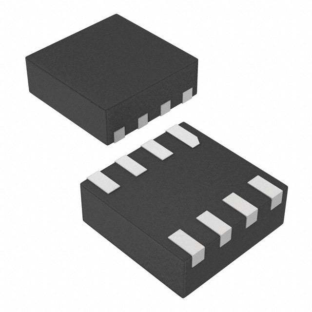
| 供应商器件封装 | 8-DFN(2x2) |
| 其它名称 | LT8410EDC-1#TRMPBFDKR |
| 包装 | Digi-Reel® |
| 同步整流器 | 无 |
| 安装类型 | 表面贴装 |
| 封装/外壳 | 8-WFDFN 裸露焊盘 |
| 工作温度 | -40°C ~ 125°C |
| 标准包装 | 1 |
| 电压-输入 | 2.5 V ~ 16 V |
| 电压-输出 | 1.235 V ~ 40 V |
| 电流-输出 | 8mA |
| 类型 | 升压(升压) |
| 输出数 | 1 |
| 输出类型 | 可调式 |
| 频率-开关 | - |


- 商务部:美国ITC正式对集成电路等产品启动337调查
- 曝三星4nm工艺存在良率问题 高通将骁龙8 Gen1或转产台积电
- 太阳诱电将投资9.5亿元在常州建新厂生产MLCC 预计2023年完工
- 英特尔发布欧洲新工厂建设计划 深化IDM 2.0 战略
- 台积电先进制程称霸业界 有大客户加持明年业绩稳了
- 达到5530亿美元!SIA预计今年全球半导体销售额将创下新高
- 英特尔拟将自动驾驶子公司Mobileye上市 估值或超500亿美元
- 三星加码芯片和SET,合并消费电子和移动部门,撤换高东真等 CEO
- 三星电子宣布重大人事变动 还合并消费电子和移动部门
- 海关总署:前11个月进口集成电路产品价值2.52万亿元 增长14.8%


PDF Datasheet 数据手册内容提取
LT8410/LT8410-1 Ultralow Power Boost Converter with Output Disconnect FEATURES DESCRIPTION n Ultralow Quiescent Current The LT®8410/LT8410-1 are ultralow power boost converters 8.5μA in Active Mode with integrated power switch, Schottky diode and output 0μA in Shutdown Mode disconnect circuitry. The parts control power delivery by n Comparator Built into SHDN Pin varying both the peak inductor current and switch off- n Low Noise Control Scheme time. This control scheme results in low output voltage n Adjustable FB Reference Voltage ripple as well as high efficiency over a wide load range. n Wide Input Range: 2.5V to 16V The quiescent current is a low 8.5μA, which is further n Wide Output Range: Up to 40V reduced to 0μA in shutdown. The internal disconnect n Integrated Power NPN Switch circuitry allows the output voltage to be blocked from the 25mA Current Limit (LT8410) input during shutdown. High value (12.4M/0.4M) resis- 8mA Current Limit (LT8410-1) tors are integrated on chip for output voltage detection, n Integrated Schottky Diode significantly reducing input referred quiescent current. The n Integrated Output Disconnect LT8410/ LT8410-1 also features a comparator built into the n High Value (12.4M/0.4M) Feedback Resistors SHDN pin, overvoltage protection for the CAP and V OUT Integrated pins, built in soft-start and comes in a tiny 8-pin 2mm × n Built in Soft-Start (Optional Capacitor from V 2mm DFN package. REF to GND) L, LT, LTC, LTM, Linear Technology and the Linear logo are registered trademarks of Linear n Overvoltage Protection for CAP and V Pins Technology Corporation. All other trademarks are the property of their respective owners. OUT Protected by U.S. Patents, including 5481178, 6580258, 6304066, 6127815, 6498466, n Tiny 8-Pin 2mm × 2mm DFN Package 6611131. APPLICATIONS n Sensor Power n RF Mems Relay Power n General Purpose Bias TYPICAL APPLICATION Output Voltage Ripple General Purpose Bias with Wide Input Voltage vs Load Current Efficiency vs Load Current 10 100 V2.I5NV to 16V 100µH VIN = 3.6V VIN = 12V V) 90 2.2µF VSCWCLT8410VCOAUPT 0.1µVFOUT = 160V.1µF* AK RIPPLE (m 86 CY (%) 80 VIN = 3.6VVIN = 5V E N 70 CENHAIPBLE SHDN VREF 604k AK-TO-P 4 EFFICIE 60 GND FBP 0.1µF PE UT 2 412k VO 50 *HIGHER VALUE CAPACITOR IS REQUIRED WHEN THE VIN IS HIGHER THAN 5V 8410-1 TA01a 0 40 0.01 0.1 1 10 0.01 0.1 1 10 100 LOAD CURRENT (mA) 8410-1 TA02 LOAD CURRENT (mA) 8410-1 TA03 84101fc 1 For more information www.linear.com/LT8410
LT8410/LT8410-1 ABSOLUTE MAXIMUM RATINGS PIN CONFIGURATION (Note 1) TOP VIEW V Voltage ................................................–0.3V to 16V CC SW Voltage ................................................–0.3V to 42V SHDN 1 8 FBP CAP Voltage ...............................................–0.3V to 40V VCC 2 7 VREF 9 GND 3 6 CAP V Voltage ..............................................–0.3V to 40V OUT SW 4 5 VOUT SHDN Voltage ............................................–0.3V to 16V V Voltage ..............................................–0.3V to 2.5V DC PACKAGE REF 8-LEAD (2mm × 2mm) PLASTIC DFN FBP Voltage ..............................................–0.3V to 2.5V TJMAX = 125°C, θJA = 88°C/W Maximum Junction Temperature ..........................125°C EXPOSED PAD (PIN #9) IS GND, MUST BE SOLDERED TO PCB Operating Temperature Range (Note 2)..–40°C to 125°C Storage Temperature Range ...................–65°C to 150°C ORDER INFORMATION (http://www.linear.com/product/LT8410#orderinfo) LEAD FREE FINISH TAPE AND REEL PART MARKING* PACKAGE DESCRIPTION TEMPERATURE RANGE LT8410EDC#PBF LT8410EDC#TRPBF LDQR 8-Lead (2mm × 2mm) Plastic DFN –40°C to 125°C LT8410IDC#PBF LT8410IDC#TRPBF LDQR 8-Lead (2mm × 2mm) Plastic DFN –40°C to 125°C LT8410EDC-1#PBF LT8410EDC-1#TRPBF LFCC 8-Lead (2mm × 2mm) Plastic DFN –40°C to 125°C LT8410IDC-1#PBF LT8410IDC-1#TRPBF LFCC 8-Lead (2mm × 2mm) Plastic DFN –40°C to 125°C Consult LTC Marketing for parts specified with wider operating temperature ranges. *The temperature grade is identified by a label on the shipping container. For more information on lead free part marking, go to: http://www.linear.com/leadfree/ For more information on tape and reel specifications, go to: http://www.linear.com/tapeandreel/. Some packages are available in 500 unit reels through designated sales channels with #TRMPBF suffix. ELECTRICAL CHARACTERISTICS The l denotes the specifications which apply over the full operating temperature range, otherwise specifications are at T = 25°C. V = 3V, V = V unless otherwise noted. (Note 2) A CC SHDN CC PARAMETER CONDITIONS MIN TYP MAX UNITS Minimum Operating Voltage 2.2 2.5 V Maximum Operating Voltage 16 V Reference Voltage l 1.220 1.235 1.255 V V Current Limit (Note 3) 10 µA REF V Discharge Time 70 µS REF V Line Regulation 0.01 %/V REF Quiescent Current Not Switching l 8.5 12 µA Quiescent Current in Shutdown V = 0V l 0 1 µA SHDN Quiescent Current from V and CAP V = 16V 3 µA OUT OUT Minimum Switch Off Time After Start-Up (Note 4) 240 nS During Start-Up (Note 4) 600 nS Switch Current Limit LT8410 l 20 25 30 mA LT8410-1 l 6 8 10 mA 84101fc 2 For more information www.linear.com/LT8410
LT8410/LT8410-1 ELECTRICAL CHARACTERISTICS The l denotes the specifications which apply over the full operating temperature range, otherwise specifications are at T = 25°C. V = 3V, V = V unless otherwise noted. (Note 2) A CC SHDN CC PARAMETER CONDITIONS MIN TYP MAX UNITS Switch V LT8410, I = 10mA 150 mV CESAT SW LT8410-1, I = 4mA 100 mV SW Switch Leakage Current V = 5V 0 1 µA SW Schottky Forward Voltage I = 10mA 650 850 mV DIODE Schottky Reverse Leakage V – V = 5 0 0.5 µA CAP SW V – V = 40 0 1 µA CAP SW PMOS Disconnect Current Limit LT8410 14 19 25 mA LT8410-1 2.5 4 5 mA PMOS Disconnect V – V I = 1mA 50 mV CAP OUT OUT V Resistor Divider Ratio l 31.6 31.85 32.2 OUT FBP Pin Bias Current V = 0.5V, Current Flows Out of Pin l 1.3 30 nA FBP SHDN Minimum Input Voltage High SHDN Rising l 1.20 1.30 1.45 V SHDN Input Voltage High Hysteresis 60 mV SHDN Hysteresis Current (Note 3) 0.08 0.1 0.14 µA SHDN Input Voltage Low 0.3 V SHDN Pin Bias Current V = 3V 0 1 µA SHDN V = 16V 2 3 µA SHDN Note 1: Stresses beyond those listed under Absolute Maximum Ratings Note 3: See the Applications Information section for more information. may cause permanent damage to the device. Exposure to any Absolute Note 4: Start-up mode occurs when V is less than V • 64/3. OUT FBP Maximum Rating condition for extended periods may affect device reliability and lifetime. Note 2: The LT8410E/LT8410E-1 are guaranteed to meet performance specifications from 0°C to 125°C junction temperature. Specifications over the –40°C to 125°C operating junction temperature range are assured by design, characterization and correlation with statistical process controls. The LT8410I/LT8410I-1 are guaranteed over the full –40°C to 125°C operating junction temperature range. TYPICAL PERFORMANCE CHARACTERISTICS T = 25°C, unless otherwise noted. A Switching Frequency vs Load Current Load Regulation V vs FBP Voltage OUT 1000 0.6 50 VCC = 3.6V VCC = 3.6V QUENCY (kHz) 860000 FVIOGUUTR =E 1 46 VCIRCUIT E CHANGE (%) 00..42 FVIOGUUTR =E 1 46 VCIRCUIT LTAGE (V) 4300 E G 0 O R A V G F 400 OLT UT 20 N V P TCHI PUT –0.2 OUT SWI 200 OUT–0.4 10 0 –0.6 0 0 1 2 3 0 1 2 3 0 0.5 1 1.5 2 LOAD CURRENT (mA) LOAD CURRENT (mA) FBP VOLTAGE (V) 8410-1 G01 8410-1 G02 8410-1 G03 84101fc 3 For more information www.linear.com/LT8410
LT8410/LT8410-1 TYPICAL PERFORMANCE CHARACTERISTICS Output Voltage vs Temperature Quiescent Current—Not Switching Quiescent Current vs Temperature 1.00 12 10 VCC = 3.6V, VOUT = 16V 0.75 LOAD = 0.5mA %) FIGURE 4 CIRCUIT 10 8 E ( 0.50 µA) µA) NG T ( 8 T ( CHA 0.25 REN REN 6 T VOLTAGE –0.250 SCENT CUR 64 SCENT CUR 4 U E E UTP–0.50 QUI QUI 2 O 2 –0.75 VCC = 3.6V –1.00 0 0 –40 0 40 80 120 0 4 8 12 16 –40 0 40 80 120 TEMPERATURE (°C) VCC VOLTAGE (V) TEMPERATURE (°C) 8410-1 G04 8410-1 G05 8410-1 G06 Quiescent Current Quiescent Current in Regulation vs SHDN Voltage with No Load SHDN Current vs SHDN Voltage 10 1000 2.5 VCC = 3.6V VCC = 3.6V 8 A) 2.0 RENT (µA) 6 RENT (µA) RRENT (µ 1.5 R R U CU CU 100 S C 1.0 QUIESCENT 24 QUIESCENT SHDN PIN BIA 0.05 VCC = 3.6V 0 10 –0.5 0 1 2 3 4 5 0 10 20 30 40 0 4 8 12 16 SHDN VOLTAGE (V) OUTPUT VOLTAGE (V) SHDN VOLTAGE (V) 8410-1 G07 8410-1 G08 8410-1 G09 Peak Inductor Current Peak Inductor Current vs Temperature (LT8410) vs Temperature (LT8410-1) V Voltage vs Temperature REF 40 15 1.235 VCC = 3.6V VCC = 3.6V mA) 36 FVIOGUUTR =E 1 46 VCIRCUIT mA) 13 FVIOGUUTR =E 1 56 VCIRCUIT 1.234 T ( T ( EN EN V) RR 32 RR 11 E (1.233 U U G R C R C LTA O O O NDUCT 28 NDUCT 9 V VREF1.232 K I K I EA 24 EA 7 1.231 P P VCC = 3.6V 20 5 1.230 –40 0 40 80 120 –40 0 40 80 120 –40 0 40 80 120 TEMPERATURE (°C) TEMPERATURE (°C) TEMPERATURE (°C) 8410-1 G10 8410-1 G11 8410-1 G12 84101fc 4 For more information www.linear.com/LT8410
LT8410/LT8410-1 TYPICAL PERFORMANCE CHARACTERISTICS LT8410 Switching Waveform LT8410 Switching Waveform at No Load at 0.5mA Load VOUT VOLTAGE VOUT VOLTAGE 2mV/DIV 10mV/DIV AC COUPLED AC COUPLED SW VOLTAGE SW VOLTAGE 10V/DIV 10V/DIV INDUCTOR INDUCTOR CURRENT CURRENT 10mA/DIV 20mA/DIV VCC = 3.6V 50µs/DIV 8410-1 G13 VCC = 3.6V 2µs/DIV 8410-1 G14 VOUT = 16V VOUT = 16V LT8410 Switching Waveform at 3mA Load UVLO vs Temperature 2.6 VOUT VOLTAGE 10mV/DIV 2.4 AC COUPLED VCC RISING V) 2.2 SW V1O0LVT/ADGIVE AGE ( VCC FALLING LT 2.0 O V INDUCTOR LO CURRENT UV 1.8 20mA/DIV 1.6 VCC = 3.6V 500ns/DIV 8410-1 G15 VOUT = 16V 1.4 –40 0 40 80 120 TEMPERATURE (°C) 8410-1 G16 SHDN Minimum Input Voltage Line Regulation High vs Temperature 0.30 1.5 VOUT = 16V %) 0.25 1.4 E ( T CHANG 0.20 M INPUGH (V) 1.3 SHDN RISING TPUT VOLTAGE 00..1150 SHDN MINIMUVOLTAGE HI 1.2 SHDN FALLING U 1.1 O 0.05 0 1.0 0 4 8 12 16 –40 0 40 80 120 VCC VOLTAGE (V) TEMPERATURE (°C) 8410-1 G17 8410-1 G18 84101fc 5 For more information www.linear.com/LT8410
LT8410/LT8410-1 TYPICAL PERFORMANCE CHARACTERISTICS Output Disconnect PMOS Current LT8410 Start-Up Waveforms vs CAP to V Voltage Difference without Capacitor at V Pin OUT REF 25 SHDN VOLTAGE VCAP = 16V 5V/DIV LT8410 20 INDUCTOR CURRENT mA) 20mA/DIV T ( 15 N E R R U OS C 10 CAP VO5LVT/ADGIVE PM VOUT VOLTAGE LT8410-1 5V/DIV 5 VCC = 3.6V 200µs/DIV 8410-1 G20 VOUT = 16V 0 0 4 8 12 16 CAP TO VOUT VOLTAGE DIFFERENCE (V) 8410-1 G19 LT8410 Start-Up Waveforms with LT8410 Transient Response 0.1μF Capacitor at V Pin 0.5mA→1.5mA→0.5mA Load Pulse REF SHDN VOLTAGE 5V/DIV VOUT VOLTAGE 200mV/DIV INDUCTOR AC COUPLED CURRENT INDUCTOR 20mA/DIV CURRENT 20mA/DIV LOAD CAP VOLTAGE CURRENT 5V/DIV 0.5mA/DIV VOUT VOLTAGE 5V/DIV VCC = 3.6V 2ms/DIV 8410-1 G21 VCC = 3.6V 2ms/DIV 8410-1 G22 VOUT = 16V VOUT = 16V SW Saturation Voltage vs Switch Current (LT8410) 300 250 V) m 200 (AT S CE 150 V H C T WI 100 S 50 0 0 5 10 15 20 25 SWITCH CURRENT (mA) 8410-1 G24 84101fc 6 For more information www.linear.com/LT8410
LT8410/LT8410-1 PIN FUNCTIONS SHDN (Pin 1): Shutdown Pin. This pin is used to enable/ V (Pin 7): Reference Pin. Soft-start can be achieved REF disable the chip. Drive below 0.3V to disable the chip. Drive by placing a capacitor from this pin to GND. This cap above 1.45V to activate the chip. Do not float this pin. will be discharged for 70µs (typical) at the beginning of start-up and then be charged to 1.235V with a 10μA V (Pin 2): Input Supply Pin. Must be locally bypassed CC current source. to GND. See the Typical Applications section. FBP (Pin 8): Positive Feedback Pin. This pin is the error GND (Pin 3): Ground. Tie directly to local ground plane. amplifier’s positive input terminal. To achieve the desired SW (Pin 4): Switch Pin. This is the collector of the inter- output voltage, choose the FBP pin voltage (V ) accord- FBP nal NPN power switch. Minimize the metal trace area ing to the following formula: connected to this pin to minimize EMI. V V = OUT V (Pin 5): Drain of Output Disconnect PMOS. Place FBP OUT 31.85 a bypass capacitor from this pin to GND. For protection purposes, the output voltage can not exceed CAP (Pin 6): Cathode of the Internal Schottky Diode. Place 40V even if V is driven higher than V . a bypass capacitor from this pin to GND. FBP REF Exposed Pad (Pin 9): Pin 9 is floating but must be ground- ed for proper shielding. BLOCK DIAGRAM 2 1 5 6 4 VCC SHDN VOUT CAP SW ENABLE MAX CHIP 10µA + 1.235V 12.4M + – OUTPUT DISCONNECT 400k VREF – 1.235V CONTROL 7 DISCHARGE CONTROL TIMING AND PEAK SWITCH CURRENT CONTROL CONTROL FB – FBP 8 + VC + 1.235V + – EXPOSED PAD (GND) GND 9 3 84101fc 7 For more information www.linear.com/LT8410
LT8410/LT8410-1 OPERATION The LT8410 series utilizes a variable peak current, variable the circuit, special precautions are taken to ensure that off-time control scheme to provide high efficiency over a the inductor current remains under control wide output current range. The LT8410 series also has a PMOS output disconnect The operation of the part can be better understood by switch. The PMOS switch is turned on when the part is referring to the Block Diagram. The part senses the output enabled via the SHDN pin. When the part is in shutdown, voltage by monitoring the internal FB node, and servoing the PMOS switch turns off, allowing the V node to OUT the FB node voltage to be equal to the FBP pin voltage. go to ground. This type of disconnect function is often The chip integrates an accurate high value resistor divider required in power supplies. (12.4M/0.4M) from the V pin. The output voltage is set OUT The differences between the LT8410 and LT8410-1 are by the FBP pin voltage, which in turn is set by an external the SW current limit and the output disconnect PMOS resistor divider from the V pin. The FBP pin voltage can REF current limit. For the LT8410, the SW current limit and also be directly biased with an external reference, allowing PMOS current limit are approximately 25mA and 19mA, full control of the output voltage during operation. respectively, while those of the LT8410-1 are approximately The switch control block senses the output of the ampli- 8mA and 4mA, respectively. fier and adjusts the switching frequency as well as other parameters to achieve regulation. During the start-up of APPLICATIONS INFORMATION Inductor Selection Table 1. Recommended Inductors for LT8410/ LT8410-1 L DCR SIZE Several inductors that work well with the LT8410 and PART (µH) (Ω) (mm) VENDOR LT8410-1 are listed in Table 1. The tables are not complete, LQH2MCN680K02 68 6.6 2.0 × 1.6 × 0.9 Murata and there are many other manufacturers and devices that LQH32CN101K53 100 3.5 3.2 × 2.5 × 2.0 www.murata.com can be used. Consult each manufacturer for more detailed DO2010-683ML 68 8.8 2.0 × 2.0 × 1.0 Coilcraft information and for their entire selection of related parts, LPS3015-104ML 100 3.4 3.0 × 3.0 × 1.4 www.coilcraft.com as many different sizes and shapes are available. LPS3015-154ML 150 6.1 3.0 × 3.0 × 1.4 LPS3314-154ML 150 4.1 3.3 × 3.3 × 1.3 Inductors with a value of 47μH or higher are recommended for most LT8410 series designs. Inductors with low core Capacitor Selection losses and small DCR (copper wire resistance) are good The small size and low ESR of ceramic capacitors make choices for LT8410 series applications. For full output them suitable for most LT8410 applications. X5R and power, the inductor should have a saturation current rating X7R types are recommended because they retain their higher than the peak inductor current. The peak inductor capacitance over wider voltage and temperature ranges current can be calculated as: than other types such as Y5V or Z5U. A 2.2μF or higher input capacitor, and a 0.1μF to 1μF output capacitor, are –6 V •150•10 I =I + IN mA sufficient for most applications. Always use a capacitor PK LIMIT L with a sufficient voltage rating. Many ceramic capacitors where the worst case I is 30mA and 10mA for LT8410 rated at 0.1μF to 1μF have greatly reduced capacitance LIMIT and LT8410-1, respectively. L is the inductance value in when bias voltages are applied. Be sure to check actual henrys and V is the input voltage to the boost circuit. capacitance at the desired output voltage. Generally, a 0603 IN 84101fc 8 For more information www.linear.com/LT8410
LT8410/LT8410-1 APPLICATIONS INFORMATION or 0805 size capacitor will be adequate. A 0.1μF to 1μF Connecting the Load to the CAP Node capacitor placed on the CAP node is recommended to filter The efficiency of the converter can be improved by con- the inductor current, while a 0.1μF to 1μF capacitor placed necting the load to the CAP pin instead of the V pin. OUT on the V node will give excellent transient response OUT and stability. To make the V pin less sensitive to noise, The power loss in the PMOS disconnect circuit is then REF putting a capacitor on the V pin is recommended, but not made negligible. No quiescent current will be consumed REF required. A 47nF to 220nF 0402 capacitor will be sufficient. in the internal feedback resistor divider string during Table 2 shows a list of several capacitor manufacturers. shutdown since the PMOS transistor will be open and the Consult the manufacturers for more detailed information internal feedback resistor divider is connected at the VOUT and for their entire selection of related parts. pin. The disadvantage of this method is that the CAP node cannot go to ground during shutdown, but will be limited Table 2. Recommended Ceramic Capacitor Manufacturers to around a diode drop below V . Loads connected to the CC MANUFACTURER PHONE WEB SITE part should only sink current. Never force external power Taiyo Yuden (408) 573-4150 www.t-yuden.com supplies onto the CAP or V pins. OUT Murata (814) 237-1431 www.murata.com AVX (843) 448-9411 www.avxcorp.com Maximum Output Load Current Kemet (408) 986-0424 www.kemet.com The maximum output current of a particular LT8410 series TDK (847) 803-6100 www.tdk.com circuit is a function of several circuit variables. The following method can be helpful in predicting the maximum load Setting Output Voltage current for a given circuit: The output voltage is set by the FBP pin voltage. V is OUT Step 1. Calculate the peak inductor current: equal to 31.85 • V when the output is regulated, as FBP shown in Figure 1. Since the VREF pin provides a good V •150•10–6 I =I + IN mA reference (1.235V), the FBP voltage can be easily set by PK LIMIT L a resistor divider from the V pin to ground. The series REF resistance of this resistor divider should be kept larger than where ILIMIT is 25mA and 8mA for LT8410 and LT8410-1 200KΩ to prevent loading down the VREF pin. The FBP pin respectively. L is the inductance value in henrys and VIN can also be biased directly by an external reference. For is the input voltage to the boost circuit. overvoltage protection, the output voltage is limited to Step 2. Calculate the inductor ripple current: 40V. Therefore, if V is higher than 1.235V, the output FBP (V +1–V )•200•10–6 voltage will stay at 40V. I = OUT IN mA RIPPLE L 50 where V is the desired output voltage. If the inductor OUT 40 ripple current is less than the peak current, then the circuit V) will only operate in discontinuous conduction mode. The E ( LTAG 30 inductor value should be increased so that IRIPPLE < IPK. VO An application circuit can be designed to operate only in T PU 20 discontinuous mode, but the output current capability T U O will be reduced. 10 Step 3. Calculate the average input current: 0 0 0.5 1 1.5 2 I FBP VOLTAGE (V) I =I – RIPPLEmA IN(AVG) PK 8410-1 F01 2 Figure 1. FBP to V Transfer Curve OUT 84101fc 9 For more information www.linear.com/LT8410
LT8410/LT8410-1 APPLICATIONS INFORMATION Step 4. Calculate the nominal output current: protection against pin glitches and slow ramping), then an internal 10μA current source pulls the V pin slowly I (cid:127)V (cid:127)0.7 REF I = IN(AVG) IN mA to 1.235V. Since the VOUT voltage is set by the FBP pin OUT(NOM) V voltage, the V voltage will also slowly increase to the OUT OUT regulated voltage, which results in lower peak inductor Step 5. Derate output current: current. The voltage ramp rate on the pin can be set by I = I • 0.8 OUT OUT(NOM) the value of the V pin capacitor. REF For low output voltages the output current capability will Output Disconnect be increased. When using output disconnect (load current taken from VOUT), these higher currents will cause the The LT8410 series has an output disconnect PMOS that drop in the PMOS switch to be higher resulting in lower blocks the load from the input during shutdown. The output current capability than predicted by the preceding maximum current through the PMOS is limited by circuitry equations. inside the chip, helping the chip survive output shorts. Inrush Current SHDN Pin Comparator and Hysteresis Current When VCC is stepped from ground to the operating voltage An internal comparator compares the SHDN pin voltage while the output capacitor is discharged, a high level of with an internal voltage reference (1.3V) which gives a inrush current may flow through the inductor and Schottky precise turn-on voltage level. The internal hysteresis of this diode into the output capacitor. Conditions that increase turn-on voltage is about 60mV. When the chip is turned on, inrush current include a larger more abrupt voltage step and the SHDN pin voltage is close to this turn-on voltage, at V , a larger output capacitor tied to the CAP pin and CC 0.1μA current flows out of the SHDN pin. This current is an inductor with a low saturation current. While the chip is called SHDN pin hysteresis current, and will go away when designed to handle such events, the inrush current should the chip is off. By connecting the external resistors as in not be allowed to exceed 0.3A. For circuits that use output Figure 2, a user-programmable enable voltage function capacitor values within the recommended range and have can be realized. input voltages of less than 6V, inrush current remains low, The turn-on voltage for the configuration is: posing no hazard to the device. In cases where there are large steps at VCC (more than 6V) and/or a large capacitor R1 is used at the CAP pin, inrush current should be measured 1.30 • 1+ R2 to ensure safe operation. and the turn-off voltage is: Soft-Start (1.24−R3•10−7)•1+R1 −(R1•10−7) The LT8410 series contains a soft-start circuit to limit R2 peak switch currents during start-up. High start-up cur- rent is inherent in switching regulators, in general, since where R1, R2 and R3 are resistance value in Ω. the feedback loop is saturated due to V being far from OUT ENABLE VOLTAGE its final value. The regulator tries to charge the output capacitor as quickly as possible, which results in large peak current. R1 R3 CONNECT TO When the FBP pin voltage is generated by a resistor divider SHDN PIN from the V pin, the start-up current can be limited by REF R2 connecting an external capacitor (typically 47nF to 220nF) to the VREF pin. When the part is brought out of shutdown, 84101 F02 this capacitor is first discharged for about 70μs (providing Figure 2. Programming Enable Voltage by Using External Resistors 84101fc 10 For more information www.linear.com/LT8410
LT8410/LT8410-1 APPLICATIONS INFORMATION Board Layout Considerations VIN SHDN As with all switching regulators, careful attention must be paid to the PCB layout and component placement. To maximize efficiency, switch rise and fall times are made as short as possible. To prevent electromagnetic interference (EMI) problems, proper layout of the high frequency SHDN FBP switching path is essential. The voltage signal of the SW pin has sharp rising and falling edges. Minimize the length and VCC VREF area of all traces connected to the SW pin and always use GND CAP a ground plane under the switching regulator to minimize GND interplane coupling. In addition, the FBP pin and V pin REF SW VOUT are sensitive to noise. Minimize the length and area of all traces to these two pins is recommended. Recommended component placement is shown in Figure 3. 8410-1 F03 CAPACITOR GROUNDS MUST BE RETURNED DIRECTLY TO IC GROUND Figure 3. Recommended Board Layout 84101fc 11 For more information www.linear.com/LT8410
LT8410/LT8410-1 TYPICAL APPLICATIONS VIN L1 Efficiency vs Load Current 2.5V to 16V 100µH 100 C1 C2 2.2µF SW CAP 0.1µF 90 VIN = 12V VCCLT8410VOUT VOUT = 16CV3 %) 80 VIN = 5V TURN ON/OFF SHDN VREF 0.1µF CY ( VIN = 3.6V 604k C0.41µF CIEN 70 GND FBP FFI E 60 412k C1: 2.2μF, 16V, X5R, 0603 8410-1 TA05 50 C2: 0.1μF, 25V, X5R, 0603 C3: 0.1μF, 25V, X5R, 0603 * 40 C4: 0.1μF, 16V, X7R, 0402 0.01 0.1 1 10 100 L1: MURATA LQH32CN101K53 * HIGHER CAPACITANCE VALUE IS REQUIRED FOR LOAD CURRENT (mA) 8410-1 TA07 C3 WHEN THE VIN IS HIGHER THAN 5V V (V) I (mA) IN OUT Figure 4. 16V Output Converter with Wide Input Voltage 3.6 2.2 5 3.6 16V Output Converter with 2mm × 2mm Inductor 12 13 VIN L1 2.5V to 16V 68µH C1 C2 Efficiency vs Load Current 2.2µF SW CAP 0.1µF 90 VCC VOUT VOUT = 16V VIN = 12V LT8410 C0.31µF 80 VIN = 5V TURN ON/OFF SHDN VREF R1 C4 %) VIN = 3.6V GND FBP 301k 0.1µF CY ( 70 N R2 E 210k FICI 60 F C1: 2.2μF, 16V, X5R, 0603 8410 TA06 E C2: 0.1μF, 25V, X5R, 0603 C3: 0.1μF, 25V, X5R, 0603 * 50 C4: 0.1μF, 16V, X7R, 0402 L1: COILCRAFT DO2010-683ML * HIGHER CAPACITANCE VALUE IS REQUIRED FOR 40 C3 WHEN THE VIN IS HIGHER THAN 5V 0.01 0.1 1 10 100 LOAD CURRENT (mA) 8410-1 TA08 LT8410 Maximum Output Current vs Output Voltage RESISTOR DIVIDER MAXIMUM OUTPUT CURRENT (mA) FROM V REF V (V) R1 (kΩ) / R2 ( kΩ) V = 2.8V V = 3.6V V = 5V V = 12V OUT IN IN IN IN 40 NA 0.5 0.7 1.1 3.6 35 110/887 0.7 0.9 1.4 4.4 30 237/768 0.8 1 1.5 5.5 25 365/634 1 1.4 2.1 7.2 20 487/511 1.4 1.9 2.9 9.7 15 619/383 1.6 2.4 4 14 10 750/255 3.3 4.6 7 NA 5 866/127 8 11 17 NA 84101fc 12 For more information www.linear.com/LT8410
LT8410/LT8410-1 TYPICAL APPLICATIONS 34V Output Converter with Wide Input Voltage Efficiency vs Load Current 90 V2.I5NV to 16V 15L01µH VIN = 12V C1 C2 80 2.2µF 0.1µF VIN = 5V SW CAP TURN ON/OFF SVHCCDLTN8410VVORUEFT 133k VOCU4T = 34C0V.31µF EFFICIENCY (%) 6700 VIN = 3.6V 0.1µF GND FBP 50 866k C1: 2.2μF, 16V, X5R, 0603 8410-1 TA09 40 C2: 0.1μF, 100V, X5R, 0603 0.01 0.1 1 10 C3: 0.1μF, 100V, X5R, 0603 * C4: 0.1μF, 16V, X7R, 0402 LOAD CURRENT (mA) 8410-1 TA10 L1: COILCRAFT LPS3314-154ML * HIGHER CAPACITANCE VALUE IS REQUIRED FOR V (V) I (mA) IN OUT C3 WHEN THE VIN IS HIGHER THAN 8V 3.6 0.8 5 1.2 12 4 VIN L1 2.5V to 16V 220µH C1 C2 2.2µF 1.0µF SW CAP VCC VOUT VOUT = 16V SHDN VOLTAGE LT8410-1 C3 2V/DIV 10000µF TURN ON/OFF SHDN VREF R1 C4 VOUT VOLTAGE 604k 0.1µF 10V/DIV GND FBP R2 INPUT CURRENT 412k 5mA/DIV C1: 2.2μF, 16V, X5R, 0603 8410-1 TA10a INDUCTOR C2: 1.0μF, 25V, X5R, 0603 * CURRENT C3: 10000μF, ELECTROLYTIC CAPACITOR 10mA/DIV C4: 0.1μF, 16V, X7R, 0402 L1: COILCRAFT LPS3008-224ML VIN = 3.6V 20s/DIV 8410-1 G10b * HIGHER CAPACITANCE VALUE IS REQUIRED FOR C2 WHEN THE VIN IS HIGHER THAN 12V Figure 5. Capacitor Charger with the LT8410-1 LT8410-1 Maximum Output Current vs Output Voltage FEEDBACK RESISTOR MAXIMUM OUTPUT CURRENT (mA) DIVIDER V (V) R1 (kΩ) / R2 ( kΩ) V = 2.8V V = 3.6V V = 5V V = 12V OUT IN IN IN IN 40 NA 0.12 0.16 0.24 0.89 35 110/887 0.14 0.19 0.3 1.1 30 237/768 0.18 0.25 0.38 1.5 25 365/634 0.25 0.35 0.55 2 20 487/511 0.34 0.48 0.76 2.9 15 619/383 0.48 0.69 1.1 3.5 10 750/255 0.84 1.2 2.1 NA 5 866/127 2.3 3.3 3.5 NA 84101fc 13 For more information www.linear.com/LT8410
LT8410/LT8410-1 PACKAGE DESCRIPTION Please refer to http://www.linear.com/product/LT8410#packaging for the most recent package drawings. DC8 Package 8-Lead Plastic DFN (2mm × 2mm) (Reference LTC DWG # 05-08-1719 Rev A) 0.70 ±0.05 2.55 ±0.05 1.15 ±0.050.64 ±0.05 (2 SIDES) PACKAGE OUTLINE 0.25 ±0.05 0.45 BSC 1.37 ±0.05 (2 SIDES) RECOMMENDED SOLDER PAD PITCH AND DIMENSIONS APPLY SOLDER MASK TO AREAS THAT ARE NOT SOLDERED R = 0.115 TYP R = 0.05 5 8 TYP 0.40 ±0.10 2.00 ±0.10 0.64 ±0.10 PIN 1 NOTCH PIN 1 BAR (4 SIDES) (2 SIDES) R = 0.20 OR TOP MARK 0.25 × 45° (SEE NOTE 6) CHAMFER (DC8) DFN 0409 REVA 4 1 0.23 ±0.05 0.200 REF 0.75 ±0.05 0.45 BSC 1.37 ±0.10 (2 SIDES) 0.00 – 0.05 BOTTOM VIEW—EXPOSED PAD NOTE: 1. DRAWING IS NOT A JEDEC PACKAGE OUTLINE 2. DRAWING NOT TO SCALE 3. ALL DIMENSIONS ARE IN MILLIMETERS 4. DIMENSIONS OF EXPOSED PAD ON BOTTOM OF PACKAGE DO NOT INCLUDE MOLD FLASH. MOLD FLASH, IF PRESENT, SHALL NOT EXCEED 0.15mm ON ANY SIDE 5. EXPOSED PAD SHALL BE SOLDER PLATED 6. SHADED AREA IS ONLY A REFERENCE FOR PIN 1 LOCATION ON THE TOP AND BOTTOM OF PACKAGE 84101fc 14 For more information www.linear.com/LT8410
LT8410/LT8410-1 REVISION HISTORY (Revision history begins at Rev B) REV DATE DESCRIPTION PAGE NUMBER B 01/11 Corrected Pin Configuration. 2 Revised Note 2 in Electrical Characteristics. 3 C 04/16 Changed SW pin voltage Absolute Maximum to 42V. 2 84101fc Information furnished by Linear Technology Corporation is believed to be accurate and reliable. 15 However, no responsibility is assumed for its use. Linear Technology Corporation makes no representa- tion that the interconneFctoiorn m ofo itrse c iinrcfuoirtsm aas tdioesnc rwibwedw h.elirneiena wr.icll onmot /inLfTri8ng4e1 o0n existing patent rights.
LT8410/LT8410-1 TYPICAL APPLICATION High Voltage Power Supply Does Not Need a Transformer DANGER HIGH VOLTAGE! OPERATION BY HIGH VOLTAGE TRAINED PERSONNEL ONLY C3, 0.1µF C5, 0.1µF VIN L1 2.5V to 16V 100µH D1 D2 D3 D4 C1 C2 C4 C6 2.2µF SW CAP 0.1µF 0.1µF 0.1µF VCC VOUT C7 LT8410 OUTPUT = 100V 0.1µF TURN ON/OFF SHDN VREF 0.4mA (VIN = 5V) 143k C8 1.4mA (VIN = 12V) C1: 2.2μF, 16V, X5R, 0603 0.1µF C2 – C7: 0.1μF, 100V, X5R, 0603 GND FBP C8: 0.1μF, 16V, X7R, 0402 787k D1 – D4: ON SEMI RB751S40T1G L1: MURATA LQH32CN101K53 8410-1 TA11 Output Voltage vs FBP Voltage Efficiency vs Load Current 140 90 VIN = 5V VOUT = 100V 120 80 VIN = 12V V) 100 E ( %) VOLTAG 80 ENCY ( 70 VIN = 5V T 60 CI OUTPU 40 EFFI 60 50 20 0 40 0 0.5 1 1.5 2 0.01 0.1 1 10 FBP VOLTAGE (V) LOAD CURRENT (mA) 8410-1 TA12 8410-1 TA13 RELATED PARTS PART NUMBER DESCRIPTION COMMENTS LT1946/LT1946A 1.5A (I ), 1.2MHz/2.7MHz, High Efficiency Step-Up DC/DC V : 2.45V to 16V, V = 34V, I = 3.2mA, I < 1µA, SW IN OUT(MAX) Q SD Converters 8-Lead MS Package LT3464 85mA (I ), High Efficiency Step-Up DC/DC Converter with V : 2.3V to 10V, V = 34V, I = 25µA, I < 1µA, SW IN OUT(MAX) Q SD Integrated Schottky and PNP Disconnect ThinSOT™ Package LT3471 Dual Output, Boost/Inverter, 1.3A (I ), High Efficiency V : 2.4V to 16V, V = ±40V, I = 2.5mA, I < 1µA, SW IN OUT(MAX) Q SD Boost-Inverting DC/DC Converter DFN Package LT3473/LT3473A 1A (I ), 1.2MHz, High Efficiency Step-Up DC/DC Converter V : 2.2V to 16V, V = 36V, I = 100µA, I < 1µA, SW IN OUT(MAX) Q SD with Integrated Schottky Diode and Output Disconnect DFN Package LT3494/LT3494A 180mA/350mA (I ), High Efficiency, Low Noise Step-Up V : 2.1V to 16V, V = 40V, I = 65µA, I < 1µA, SW IN OUT(MAX) Q SD DC/DC Converter with Output Disconnect DFN Package LT3495/LT3495B/ 650mA/350mA (I ), High Efficiency, Low Noise Step-Up V : 2.3 V to 16V, V = 40V, I = 60µA, I < 1µA, SW IN OUT(MAX) Q SD LT3495-1/LT3495B-1 DC/DC Converter with Output Disconnect DFN Package 84101fc 16 Linear Technology Corporation LT 0416 REV C • PRINTED IN USA 1630 McCarthy Blvd., Milpitas, CA 95035-7417 For more information www.linear.com/LT8410 (408) 432-1900 ● FAX: (408) 434-0507 ● www.linear.com/LT8410 LINEAR TECHNOLOGY CORPORATION 2008