ICGOO在线商城 > 集成电路(IC) > 线性 - 放大器 - 视频放大器和频缓冲器 > LT6551IMS#PBF

 Datasheet下载
- 型号: LT6551IMS#PBF
- 制造商: LINEAR TECHNOLOGY
- 库位|库存: xxxx|xxxx
- 要求:
| 数量阶梯 | 香港交货 | 国内含税 |
| +xxxx | $xxxx | ¥xxxx |
查看当月历史价格
查看今年历史价格
LT6551IMS#PBF产品简介:
ICGOO电子元器件商城为您提供LT6551IMS#PBF由LINEAR TECHNOLOGY设计生产,在icgoo商城现货销售,并且可以通过原厂、代理商等渠道进行代购。 LT6551IMS#PBF价格参考。LINEAR TECHNOLOGYLT6551IMS#PBF封装/规格:线性 - 放大器 - 视频放大器和频缓冲器, Video Amp, 4 电压反馈 10-MSOP。您可以下载LT6551IMS#PBF参考资料、Datasheet数据手册功能说明书,资料中有LT6551IMS#PBF 详细功能的应用电路图电压和使用方法及教程。
LT6551IMS#PBF 是 Analog Devices(原 Linear Technology)推出的一款高性能视频放大器和频率缓冲器,主要应用于需要高质量信号传输和处理的场合。其典型应用场景包括:

1. 视频信号传输系统:适用于高清视频信号的放大与缓冲,支持多种视频格式,如NTSC、PAL、S-Video和RGB视频信号,广泛用于专业视频设备和工业摄像系统。

2. 图像采集设备:用于摄像头、医疗成像设备、工业相机等产品中,提升视频信号的驱动能力和传输稳定性,确保图像清晰无失真。

3. 通信与广播设备:在广播级视频处理设备、视频分配器和切换器中用作缓冲放大器,以增强信号强度并驱动长距离传输线路。

4. 测试与测量仪器:如示波器、视频分析仪等设备中,用于对视频信号进行精确放大和整形,保证测试信号的完整性。

5. 安防监控系统:用于视频监控系统中的信号调理,增强视频信号的抗干扰能力,提升远距离传输质量。

LT6551具备低功耗、高带宽(可达220MHz)、低失真和良好的驱动能力,适合在要求高性能和稳定性的模拟视频信号处理中使用。
| 参数 | 数值 |
| -3db带宽 | 90MHz |
| 产品目录 | 集成电路 (IC) |
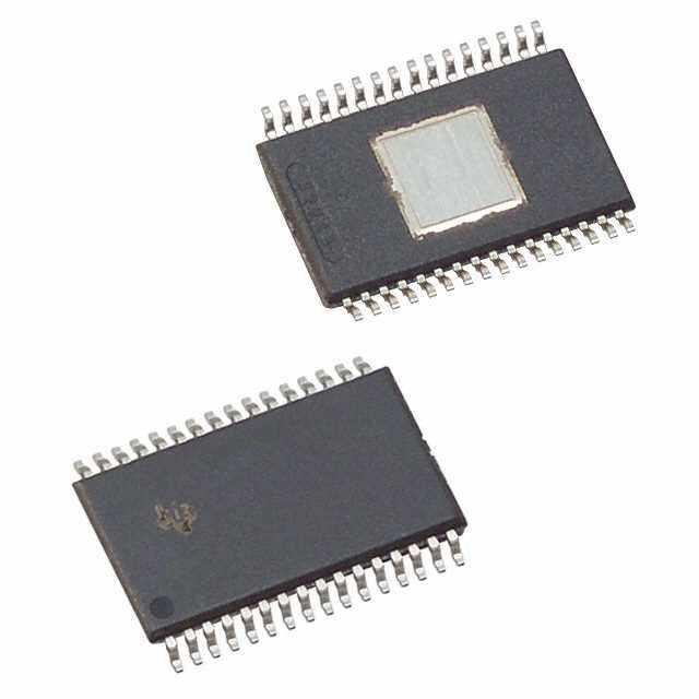
| 描述 | IC AMP VIDEO QUAD 3.3V 10-MSOP |
| 产品分类 | |
| 品牌 | Linear Technology |
| 数据手册 | http://www.linear.com/docs/3984 |
| 产品图片 |
|
| 产品型号 | LT6551IMS#PBF |
| rohs | 无铅 / 符合限制有害物质指令(RoHS)规范要求 |
| 产品系列 | - |
| 供应商器件封装 | 10-MSOP |
| 其它名称 | LT6551IMSPBF |
| 包装 | 管件 |
| 压摆率 | 600 V/µs |
| 安装类型 | 表面贴装 |
| 封装/外壳 | 10-TFSOP,10-MSOP(0.118",3.00mm 宽) |
| 应用 | 电压反馈 |
| 标准包装 | 50 |
| 电压-电源,单/双 (±) | 3 V ~ 12.6 V |
| 电流-电源 | 8.5mA |
| 电流-输出/通道 | 60mA |
| 电路数 | 4 |
| 输出类型 | 满摆幅 |


- 商务部:美国ITC正式对集成电路等产品启动337调查
- 曝三星4nm工艺存在良率问题 高通将骁龙8 Gen1或转产台积电
- 太阳诱电将投资9.5亿元在常州建新厂生产MLCC 预计2023年完工
- 英特尔发布欧洲新工厂建设计划 深化IDM 2.0 战略
- 台积电先进制程称霸业界 有大客户加持明年业绩稳了
- 达到5530亿美元!SIA预计今年全球半导体销售额将创下新高
- 英特尔拟将自动驾驶子公司Mobileye上市 估值或超500亿美元
- 三星加码芯片和SET,合并消费电子和移动部门,撤换高东真等 CEO
- 三星电子宣布重大人事变动 还合并消费电子和移动部门
- 海关总署:前11个月进口集成电路产品价值2.52万亿元 增长14.8%


PDF Datasheet 数据手册内容提取
LT6550/LT6551 3.3V Triple and Quad Video Amplifiers FEATURES DESCRIPTIOU ■ Single Supply Operation from 3V to 12.6V The LT®6550/LT6551 are 3.3V triple and quad high speed ■ Small (3mm × 5mm) MSOP 10-Lead Package video amplifiers. These voltage feedback amplifiers drive ■ Internal Resistors for a Gain of Two double terminated 50Ω or 75Ω cables and are configured ■ 340V/µs Slew Rate for a fixed gain of 2, eliminating six or eight external gain ■ 110MHz –3dB Bandwidth setting resistors. The LT6550/LT6551 feature 110MHz ■ 30MHz Flat to 0.25dB –3dB bandwidth, high slew rates and fast settling, making ■ 3% Settling Time: 20ns them ideal for RGB video processing. ■ Input Common Mode Range Includes Ground The LT6551 quad is designed for single supply operation ■ Rail-to-Rail Output and the LT6550 triple can be used on either single or split ■ High Output Drive: 60mA supplies. On a single 3.3V supply, the input voltage range ■ Operating Temperature Range: –40°C to 85°C extends from ground to 1.55V and the output swings to ■ 24-Bit RGB within 400mV of the supply voltage while driving a 150Ω APPLICATIOU S load. These features, combined with the ability to accept RGB video signals without the need for AC coupling or ■ Automotive Displays level shifting of the incoming signals, make the LT6550/ ■ LCD and CRT Compatible LT6551 an ideal choice for low voltage video applications. ■ RGB Amplifiers Both the LT6550 and LT6551 are available in the small ■ Coaxial Cable Drivers 10-Pin MSOP package and utilize a flow-thru pin out. The ■ Low Voltage High Speed Signal Processing small footprint results in a compact high performance ■ Set Top Boxes video amplifier solution. , LTC and LT are registered trademarks of Linear Technology Corporation. All other trademarks are the property of their respective owners. TYPICAL APPLICATIOU 3.3V Single Supply LT6551 RGB Plus SYNC Cable Driver LT6551 RIN 450Ω 450Ω 3.3V Output Step Response 75Ω – OA + ROUT 75Ω 450Ω 450Ω GIN 75Ω VOUT 75Ω – OA + GOUT 75Ω 450Ω 450Ω BIN 75Ω 75Ω – 0V OA + BOUT 75Ω VIN 450Ω 450Ω SYNCIN 75Ω 0V 75Ω – VS = 3.3V 6550/51 TA01b OA VIN = 0.5V TO 1.25V + 75Ω f = 10MHz GND SYNCOUT 75Ω 6551 TA01a 65501fa 1
LT6550/LT6551 ABSOLUTE WAXIWUW RATIUGS (Note 1) Total Supply Voltage Specified Temperature Range (Note 3) LT6550 (V TO V )........................................ 12.6V LT6550C/LT6551C ..............................–40°C to 85°C CC EE LT6551 (V TO GND)...................................... 12.6V LT6550I/LT6551I................................ –40°C to 85°C CC Input Current (Note 9)........................................ ±10mA Maximum Junction Temperature..........................150°C Output Short-Circuit Duration (Note 2)............Indefinite Storage Temperature Range................. –65°C to 150°C Operating Temperature Range................ –40°C to 85°C Lead Temperature (Soldering, 10 sec)..................300°C PACKAGE/ORDER IUFORWATIOU TOP VIEW TOP VIEW IN1 1 X2 10 VCC IN1 1 X2 10 VCC IN2 2 X2 9 OUT1 IN2 2 X2 9 OUT1 IN3 3 X2 8 OUT2 IN3 3 X2 8 OUT2 GND 4 7 OUT3 IN4 4 X2 7 OUT3 VEE 5 6 N/C GND 5 6 OUT4 MS10 PACKAGE MS10 PACKAGE 10-LEAD PLASTIC MSOP 10-LEAD PLASTIC MSOP TJMAX = 150°C, θJA = 110°C/W TJMAX = 150°C, θJA = 110°C/W (Note 4) (Note 4) ORDER PART NUMBER MS10 PART MARKING ORDER PART NUMBER MS10 PART MARKING LT6550CMS LTB9 LT6551CMS LTC2 LT6550IMS LTC1 LT6551IMS LTC3 Order Options Tape and Reel: Add #TR Lead Free: Add #PBF Lead Free Tape and Reel: Add #TRPBF Lead Free Part Marking: http://www.linear.com/leadfree/ Consult LTC Marketing for parts specified with wider operating temperature ranges. 3.3V ELECTRICAL CHARACTERISTICS The ● denotes the specifications which apply over the specified temperature range, otherwise specifications are at TA = 25°C. VCC = 3.3V, VGND = 0V; VIN = 0.75V LT6550 (Pins 1,2,3); LT6551 (Pins 1,2,3,4). V = 0V LT6550 (Pin 5), unless otherwise noted. EE PARAMETER CONDITIONS MIN TYP MAX UNITS DC Output Accuracy No Load, V Ideal = 1.5V ● 30 70 mV OUT Output Voltage Matching Between Any Two Outputs ● 25 75 mV Input Current Any Input ● 15 65 µA Input Impedance, ∆VIN/∆IIN VIN = 0V to 1V ● 100 300 kΩ Input Noise Voltage Density f = 100kHz (Note 10) 12 nV/√Hz Input Noise Current Density f = 100kHz (Note 10) 8 pA/√Hz Voltage Gain (Note 5) 0.25V ≤ VIN ≤ 1.25V No Load ● 1.9 2.1 V/V RL = 150Ω ● 1.9 2.1 V/V RL = 75Ω, 0.25V ≤ VIN ≤ 0.75V 1.85 2.15 V/V Output Voltage Swing Low V = –0.1V IN No Load ● 10 30 mV I = 5mA ● 60 150 mV SINK I = 10mA ● 90 200 mV SINK 65501fa 2
LT6550/LT6551 3.3V ELECTRICAL CHARACTERISTICS The ● denotes the specifications which apply over the specified temperature range, otherwise specifications are at TA = 25°C. VCC = 3.3V, VGND = 0V; VIN = 0.75V LT6550 (Pins 1,2,3); LT6551 (Pins 1,2,3,4). V = 0V LT6550 (Pin 5), unless otherwise noted. EE PARAMETER CONDITIONS MIN TYP MAX UNITS Output Voltage Swing High V = 1.75V IN No Load ● 3.0 3.2 V RL = 150Ω ● 2.5 2.9 V RL = 75Ω 2.0 2.5 V PSRR V = 3V to 10V, V = 0.5V ● 40 48 dB CC IN Minimum Supply Voltage (Note 6) ● 3 V Output Short-Circuit Current V = 1V, V = 0V 35 50 mA IN OUT ● 25 mA Supply Current per Amplifier (Note 7) 8.5 10 mA ● 11 mA Slew Rate (Note 8) RL = 150Ω, VOUT = 0.5V to 2.5V 140 250 V/µs Measured from 1V to 2V ● 115 V/µs Small Signal –3dB Bandwidth RL = 150Ω 90 MHz Gain Flatness Less than 0.25dB 30 MHz Gain Matching Any One Channel to Any Other Channel 0.15 dB Settling Time to 3% RL = 150Ω, VOUT = 1V to 2.5V 20 ns Settling Time to 1% RL = 150Ω, VOUT = 1V to 2.5V 30 ns % Overshoot VOUT = 1V to 2.5V, RL = 150Ω 5 % Differential Gain RL = 150Ω, Black Level = 0.6V at Device Output 0.09 % Differential Phase RL = 150Ω, Black Level = 0.6V at Device Output 0.09 Deg Channel Separation Measured at 10MHz 60 dB 5V ELECTRICAL CHARACTERISTICS The ● denotes the specifications which apply over the specified temperature range, otherwise specifications are at TA = 25°C. VCC = 5V, VGND = 0V; VIN = 1.25V LT6550 (Pins 1,2,3); LT6551 (Pins 1,2,3,4). V = 0V LT6550 (Pin 5), unless otherwise noted. EE PARAMETER CONDITIONS MIN TYP MAX UNITS Output Accuracy No Load, V Ideal = 2.5V ● 30 70 mV OUT Output Voltage Matching Between Any Two Outputs ● 40 90 mV Input Current ● 15 65 µA Input Impedance, ∆VIN/∆IIN VIN = 0V to 2V ● 100 300 kΩ Input Noise Voltage Density f = 100kHz (Note 10) 12 nV/√Hz Input Noise Current Density f = 100kHz (Note 10) 8 pA/√Hz Voltage Gain (Note 5) 0.25V ≤ VIN ≤ 1.75V No Load ● 1.9 2.1 V/V RL = 150Ω ● 1.9 2.1 V/V RL = 75Ω, 0.25V ≤ VIN ≤ 1.25V, 0°C ≤ TA ≤ 70°C (Only) ● 1.85 2.15 V/V Output Voltage Swing Low V = –0.1V IN No Load ● 10 30 mV I = 5mA ● 60 150 mV SINK I = 10mA ● 90 200 mV SINK Output Voltage Swing High V = 2.6V IN No Load ● 4.6 4.8 V RL = 150Ω ● 3.5 4.1 V RL = 75Ω, 0°C ≤ TA ≤ 70°C (Only) ● 2.5 3.2 V 65501fa 3
LT6550/LT6551 5V ELECTRICAL CHARACTERISTICS The ● denotes the specifications which apply over the specified temperature range, otherwise specifications are at TA = 25°C. VCC = 5V, VGND = 0V; VIN = 1.25V LT6550 (Pins 1,2,3); LT6551 (Pins 1,2,3,4). V = 0V LT6550 (Pin 5), unless otherwise noted. EE PARAMETER CONDITIONS MIN TYP MAX UNITS PSRR V = 3V to 10V, V = 0.5V ● 40 48 dB CC IN Minimum Supply Voltage (Note 6) ● 3 V Output Short-Circuit Current V = 1V, V = 0V 45 60 mA IN OUT 0°C ≤ TA ≤ 70°C ● 40 mA –40°C ≤ TA ≤ 85°C ● 30 mA Supply Current per Amplifier (Note 7) 9.5 11.5 mA ● 12.5 mA Slew Rate RL = 150Ω, VOUT = 0.5V to 3.5V, 220 340 V/µs Measured from 1V to 3V ● 180 V/µs Small Signal –3dB Bandwidth RL = 150Ω 110 MHz Gain Flatness Less than 0.25dB 30 MHz Gain Matching Any One Channel to Any Other Channel 0.15 dB Settling Time to 3% RL = 150Ω, VOUT = 1V to 2.5V 20 ns Settling Time to 1% RL = 150Ω, VOUT = 1V to 2.5V 35 ns % Overshoot VOUT = 1V to 2.5V, RL = 150Ω 5 % Differential Gain RL = 150Ω, Black Level = 1V at Device Output 0.05 % Differential Phase RL = 150Ω, Black Level = 1V at Device Output 0.05 Deg Channel Separation Measured at 10MHz 60 dB ±5V ELECTRICAL CHARACTERISTICS (LT6550 Only) The ● denotes the specifications which apply over the specified temperature range, otherwise specifications are at TA = 25°C. VS = ±5V, VIN = 0V (Pins 1,2,3) VGND = 0V (Pin 4) unless otherwise noted. PARAMETER CONDITIONS MIN TYP MAX UNITS Output Offset ● 30 70 mV Output Voltage Matching Between Any Two Outputs ● 20 60 mV Input Current ● 20 70 µA Input Impedance, ∆VIN/∆IIN VIN = –1V to 1V ● 200 500 kΩ Input Noise Voltage Density f = 100kHz (Note 10) 12 nV/√Hz Input Noise Current Density f = 100kHz (Note 10) 8 pA/√Hz Voltage Gain –1.75V ≤ VIN ≤ 1.75V No Load ● 1.9 2.1 V/V RL = 150Ω ● 1.9 2.1 V/V RL = 75Ω, –1V ≤ VIN ≤ 1V ● 1.9 2.1 V/V Output Voltage Swing VIN = ±2.6V No Load ● ±4.6 ±4.8 V RL = 150Ω ● ±3.5 ±4.2 V RL = 75Ω, 0°C ≤ TA ≤ 70°C (Only) ● ±2.6 ±3.2 V PSRR VS = ±2.5V to ±5V, ● 38 48 dB Output Short-Circuit Current V = 0V 45 60 mA O 0°C ≤ TA ≤ 70°C ● 40 mA –40°C ≤ TA ≤ 85°C ● 30 mA 65501fa 4
LT6550/LT6551 ±5V ELECTRICAL CHARACTERISTICS (LT6550 Only) The ● denotes the specifications which apply over the specified temperature range, otherwise specifications are at TA = 25°C. VS = ±5V, VIN = 0V (Pins 1,2,3) VGND = 0V (Pin 4) unless otherwise noted. PARAMETER CONDITIONS MIN TYP MAX UNITS Supply Current per Amplifier 8.5 10.5 mA ● 12 mA Slew Rate RL = 150Ω, VOUT = –3V to 3V, 400 600 V/µs Measured from –2V to 2V ● 300 V/µs Small Signal –3dB Bandwidth RL = 150Ω 90 MHz Gain Flatness Less than 0.25dB 30 MHz Gain Matching Any One Channel to Any Other Channel 0.15 dB Settling Time to 3% RL = 150Ω, VOUT = 1V to 2.5V 20 ns Settling Time to 1% RL = 150Ω, VOUT = 1V to 2.5V 30 ns % Overshoot VOUT = 1V to 2.5V, RL = 150Ω 5 % Differential Gain RL = 150Ω, Black Level = 0V at Device Output 0.15 % Differential Phase RL = 150Ω, Black Level = 0V at Device Output 0.09 Deg Channel Separation Measured at 10MHz 60 dB Note 1: Absolute Maximum Ratings are those values beyond which the life Note 4: Thermal resistance varies depending upon the amount of PC board of a device may be impaired. metal attached to Pin 5 of the device. θJA is specified for a 2500mm2 test Note 2: A heat sink may be required to keep the junction temperature board covered with 2oz copper on both sides. below absolute maximum. This depends on the power supply voltage and Note 5: Gain is measured by changing the input voltage, and dividing the how many amplifiers are shorted. change in output voltage by the change in input voltage. Note 3: The LT6550C/LT6551C are guaranteed to meet specified Note 6: Minimum supply voltage is guaranteed by the PSRR test. performance from 0°C to 70°C and are designed, characterized and Note 7: The supply current specification includes additional output current expected to meet specified performance from –40°C to 85°C but are not through the internal feedback and gain resistor. tested or QA sampled at these temperatures. The LT6550I/LT6551I are Note 8: Guaranteed by correlation to slew rate at 5V and ±5V. guaranteed to meet specified performance from –40°C to 85°C. Note 9: The inputs are protected from ESD with diodes to the supplies. Note 10: Noise is input referred, including internal gain resistors. 5V/3.3V TYPICAL PERFORW AU CE CHARACTERISTICS V (Pin 5) = 0V (LT6550), GND (Pin 5) = 0V (LT6551) EE Supply Current Per Amplifier vs Input Bias Current vs Supply Voltage Output Voltage vs Input Voltage Temperature 14 3.5 –10 12 VRGILNN D= = ∞ =0 .07V5V TA = 25°C TA = 125°C 3.0 VRSL == 31.530VΩ, 0V TA = 125°CTA = 25°C –11 VVSO U=T 5=V 2, .05VV –12 mA) 10 2.5 TA = –55°C –13 URRENT ( 8 TA = –55°C (V)UT 2.0 BIAS (A)µ––1145 Y C 6 VO 1.5 UT –16 L P P N UP 4 1.0 I –17 S –18 2 0.5 –19 0 0 –20 0 1 2 3 4 5 6 7 8 9 10 0 0.2 0.4 0.6 0.8 1.0 1.2 1.4 1.6 1.8 2.0 –50 –25 0 25 50 75 100 125 VCC (V) VIN (V) TEMPERATURE (°C) 6550/51 G01 6550/51 G02 6550/51 G03 65501fa 5
LT6550/LT6551 5V/3.3V TYPICAL PERFORW AU CE CHARACTERISTICS V (Pin 5) = 0V (LT6550), GND (Pin 5) = 0V (LT6551) EE Input Bias Current vs Input Input Bias Current vs Input Output Saturation Voltage vs Voltage Voltage Load Current (Output High) 0 0 1 VS = 3.3V, 0V VS = 5V, 0V VS = 5V, 0V VIN = 2.6V A) –5 TA = 125°C A) –5 TA = 125°C GE (V) µ µ A NT ( NT ( –10 OLT TA = 125°C INPUT BIAS CURRE –––112050 TA = –55°TCA = 25°C INPUT BIAS CURRE –––122505 TA = –T5A5 =° C25°C UTPUT SATURATION V 0.1 TA =T A– 5=5 2°C5°C O –25 –30 0.01 0 0.2 0.4 0.6 0.8 1.0 1.2 1.4 1.6 0 0.5 1.0 1.5 2.0 2.5 0.01 0.1 1 10 100 INPUT VOLTAGE (V) INPUT VOLTAGE (V) SOURCING LOAD CURRENT (mA) 6550/51 G04 6550/51 G05 6550/51 G06 Output Saturation Voltage vs Output Short-Circuit Current Load Current (Output Low) vs Temperature Gain and Phase vs Frequency 1 90 10 0 OLTAGE (V) VVSIN = = 5 –V0, .01VV URRENT (mA) 887505 VIN = 1V VS = 5V, 0V 987 RVVSOL U==T 31=.5 310V.Ω5, V0 VDC PHASE –––246000 TPUT SATURATION V 0.1 TA = 25°CTA T=A 1 =2 5–°5C5°C UT SHORT-CIRCUIT C 76650505 VS = 3.3V, 0V GAIN (dB) 65432 GAIN –––––81111002460000PHASE (DEG) U P O UT 50 1 –180 O 0.01 45 0 –200 0.01 0.10 1 10 100 –50 –25 0 25 50 75 100 125 10k 100k 1M 10M 100M500M SINKING LOAD CURRENT (mA) TEMPERATURE (°C) FREQUENCY (Hz) 6550/51 G07 6550/51 G08 6550/51 GO9 –3dB, –0.25dB Bandwidth vs Gain Flatness vs Frequency Temperature –3dB Bandwidth vs VCC 6.2 140 180 VS = 3.3V, 0V VOUT = 1.5V DC VOUT = 1.5V DC VOUT = 1.5V DC 120 RL = 150Ω GND = 0V 6.1 RL = 150Ω 5V, 0V, –3dB 160 RL = 150Ω dB) 6.0 H (MHz) 10800 3.3V, 0V, –3dB DTH (MHz) 140 N ( DT WI GAI 5.9 DWI 60 5V, 0V, –0.25dB AND 120 N B BA 40 dB 3 5.8 – 100 3.3V, 0V, –0.25dB 20 5.7 0 80 10k 100k 1M 10M 100M –50 –25 0 25 50 75 100 125 3 4 5 6 7 8 9 10 11 12 FREQUENCY (Hz) TEMPERATURE (°C) VCC (V) 6550/51 G10 6550/51 G11 6550/51 G12 65501fa 6
LT6550/LT6551 5V/3.3V TYPICAL PERFORW AU CE CHARACTERISTICS V (Pin 5) = 0V (LT6550), GND (Pin 5) = 0V (LT6551) EE Frequency Response with Capacitive Load Handling, Capacitive Loads Overshoot vs Capacitive Load Slew Rate vs Temperature 12 45 500 VS = 5V, 0V VS = 5V, 0V RL = 150Ω 1110 VROL U=T 1=5 20.Ω5V DC CL = 150pF 4305 450 5V, 0V, RISING 9 CL = 100pF %) 30 RL = OPEN s)µ 400 GAIN (dB) 8765 CL = 50CpLF = 10pF OVERSHOOT ( 221505 RL = 150Ω SLEW RATE (V/ 332505000 5V, 0V,3 F.3AVL,L 0INVG, RISING 4 10 3.3V, 0V, FALLING 200 3 5 2 0 150 10k 100k 1M 10M 100M500M 10 100 1000 –50 –25 0 25 50 75 100 125 FREQUENCY (Hz) CAPACITIVE LOAD (pF) TEMPERATURE (°C) 6550/51 G13 6550/51 G14 6550/51 G15 Power Supply Rejection Ratio vs Frequency Output Impedance vs Frequency Channel Separation vs Frequency 60 100 100 dB) VVSO U=T 5=V 2, .05VV DC VVSO U=T 5=V 2, .05VV DC 90 VRSL == 51V50, Ω0V O ( 50 +PSSR RL = 150Ω 80 ANY CHANNEL PAIR N RATI 40 E ()Ω 10 70 O C REJECTI 30 MPEDAN AIN(dB) 6500 WER SUPPLY 2100 OUTPUT I 1 G 432000 O 10 P 0 0.1 0 10k 100k 1M 10M 100M 1000M 10k 100k 1M 10M 100M 10k 100k 1M 10M 100M 1000M FREQUENCY (Hz) FREQUENCY (Hz) FREQUENCY (Hz) 6550/51 G16 6550/51 G17 6550/51 G18 2nd and 3rd Harmonic Distortion Gain Matching vs Frequency vs Frequency Small Signal Response 0 –30 VS = 3.3V, 0V VO = 2VP-P (0.5V TO 2.5V) –0.2 –40 RL = 150Ω dB) c)–50 ATCHING(–0.4 RTION (dB–60 2ND M–0.6 O GAIN DIST–70 3RD –0.8 VS = 3.3V, 0V –80 CL = 20pF 6550/51 G21 VOUT = 1.5V DC, ANY CHANNEL PAIR VS = 5V, 0V –1.0 –90 VOUT = 2.5V DC 10k 100k 1M 10M 100M 1000M 100k 1M 10M RL = 150Ω FREQUENCY (Hz) FREQUENCY (Hz) 6550/51 G19 6550/51 G20 (cid:31) 65501fa 7
LT6550/LT6551 5V/3.3V TYPICAL PERFORW AU CE CHARACTERISTICS V (Pin 5) = 0V (LT6550), GND (Pin 5) = 0V (LT6551) EE Large Signal Response CL = 20pF 6550/51 G22 VS = 5V, 0V VOUT = 0.5V TO 3.5V RL = 150Ω ±5V TYPICAL PERFORW AU CE CHARACTERISTICS (LT6550 Only) V (Pin 4) = 0V GND Supply Current vs Total Supply Input Bias Current vs Input Output Offset Voltage vs Voltage Voltage Temperature of Three Typical Units 14 –10 60 VOUT = 0V VS = ±5V VS = ±5V 12 50 VIN = 0V UPPLY CURRENT (mA) 18640 TA =T TA1 A2= =5 – °25C55°°CC UT BIAS CURRENT (A)µ ––1250 TA = 25°C TAT =A =1 2–55°5C°C UT OFFSET VOLTAGE (mV) 43210000 S NP –25 TP 0 I U 2 O –10 0 –30 –20 0 ±1 ±2 ±3 ±4 ±5 ±6 –2.5–2.0–1.5–1.0–0.5 0 0.5 1.0 1.5 2.0 2.5 –50 –25 0 25 50 75 100 125 TOTAL SUPPLY VOLTAGE (V) INPUT VOLTAGE (V) TEMPERATURE (°C) 6550/51 G23 6550/51 G24 6550/51 G25 Output Voltage Matching vs Output Short-Circuit Current Temperature of Three Typical Parts vs Temperature Gain and Phase vs Frequency 25 95 10 0 G (mV) 20 VVASINN Y= = C± 0H5VVANNEL PAIR ENT (mA) 90 VVSIN = = ± ±51VV 98 PHASE ––2400 MATCHIN 15 UIT CURR 85 SINKING dB) 76 GAIN ––6800 PHAS UTPUT VOLTAGE 150 PUT SHORT-CIRC 8705 SOURCING GAIN( 5432 VS = ±5V ––––111102460000E (DEG) O UT 1 VOUT = 0V DC –180 O RL = 150Ω 0 70 0 –200 –50 –25 0 25 50 75 100 125 –50 –25 0 25 50 75 100 125 10k 100k 1M 10M 100M 1000M TEMPERATURE (°C) TEMPERATURE (°C) FREQUENCY (Hz) 6550/51 G26 6550/51 G27 6550/51 G28 65501fa 8
LT6550/LT6551 ±5V TYPICAL PERFORW AU CE CHARACTERISTICS (LT6550 Only) V (Pin 4) = 0V GND Frequency Response with Gain Flatness vs Frequency Gain Matching vs Frequency Capacitive Loads 6.2 0 12 VS = ±5V VS = ±5V VOUT = 0V DC 11 VOUT = 0V DC 6.1 RL = 150Ω –0.2 10 RL = 150Ω CL = 150pF B) 9 dB) 6.0 HING(d–0.4 dB) 8 CCL L= =1 0500ppFF N ( TC N ( 7 GAI 5.9 MA–0.6 GAI 6 GAIN 5 CL = 10pF 5.8 –0.8 4 VS = ±5V 3 ANY CHANNEL PAIR 5.7 –1.0 2 10k 100k 1M 10M 100M 10k 100k 1M 10M 100M 1000M 10k 100k 1M 10M 100M500M FREQUENCY (Hz) FREQUENCY (Hz) MM FREQUENCY (Hz) 6550/51 G29 6550/51 G30 6550/51 G31 Power Supply Rejection Ratio vs Slew Rate Frequency Output Impedance vs Frequency 800 60 100 VS = ±5V VS = ±5V VS = ±5V 750 RL = 150Ω O (dB) 50 VROL U=T 1=5 00VΩ DC VOUT = 0V DC SLEW RATE (/V s)µ 766050000 RFISAILNLGING R SUPPLY REJECTION RATI 43210000 +PSRR –PSRR OUTPUT IMPEDANCE ()Ω 101 550 WE 0 O P 500 –10 0.1 –50 –25 0 25 50 75 100 125 10k 100k 1M 10M 100M 1000M 10k 100k 1M 10M 100M TEMPERATURE (°C) FREQUENCY (Hz) FREQUENCY (Hz) 6550/51 G32 6550/51 G33 6550/51 G34 2nd and 3rd Harmonic Distortion Channel Separation vs Frequency vs Frequency Large Signal Response 100 –30 VS = ±5V VS = ±5V 90 RL = 150Ω VO = 2VP-P 80 ANY CHANNEL PAIR –40 RL = 150Ω 70 c)–50 B GAIN (dB) 654000 TORTION (d–60 2ND3RD 0V 30 DIS–70 20 –80 CL = 20pF 6550/51 G37 10 VS = ±5V 0 –90 RL = 150Ω 10k 100k 1M 10M 100M 1000M 100k 1M 10M FREQUENCY (Hz) FREQUENCY (Hz) 6550/51 G35 6550/51 G36 (cid:31) 65501fa 9
LT6550/LT6551 BLOCK DIAGRAW S LT6550 Block Diagram LT6551 Block Diagram 450Ω 450Ω 450Ω 450Ω IN1 IN1 VCC VCC – – OA OA + + OUT1 OUT1 450Ω 450Ω 450Ω 450Ω IN2 IN2 – – OA OA + + OUT2 OUT2 450Ω 450Ω 450Ω 450Ω IN3 IN3 – – OA OA + + OUT3 OUT3 450Ω 450Ω GND IN4 – OA + VEE N/C GND OUT4 6550 BD01 6551 BD02 65501fa 10
LT6550/LT6551 APPLICATIOUS IUFORWATIOU Amplifier Characteristics Figure 1 shows a simplified schematic of one channel of the maximum input is (3V – 1.75V) or 1.25V, and the the LT6551 quad. Resistors RF and RG provide an internal internal gain of two will set the output voltage to 2.5V. gain of 2. (The LT6550 triple is a slight variation with the Increasing the input beyond 1.25V will force the device out gain setting resistor, RG, connected to a separate ground of its linear range, no longer a gain of 2, and the output will pin). The input stage consists of transistors Q1 to Q8 and not increase beyond 2.5V. At a higher supply voltage, i.e. resistor R1. This topology allows for high slew rates at low 5V, the maximum input voltage is 5V – 1.75V or 3.25V. supply voltages. There are back-to-back series diodes, D1 However, due to the internal gain of 2, the output will clip to D4, across the + and – inputs of each amplifier to limit with a lower input voltage. For linear unclipped operation the differential input voltage to ±1.4V. R limits the the minimum input voltage is (V Min)/2 and the maxi- IN OUT current through these diodes if the input differential volt- mum input voltage is (V Max)/2 or (V – 1.75V), OUT CC age exceeds ±1.4V. The input stage drives the degenera- whichever is less. tion resistors of PNP and NPN current mirrors, Q9 to Q12, that convert the differential signals into a single-ended ESD output. The complementary drive generator supplies cur- The LT6550/LT6551 have reverse-biased ESD protection rent to the output transistors that swing from rail-to-rail. diodes on all inputs and outputs as shown in Figure 1. If these pins are forced beyond either supply, unlimited Input Voltage Range current will flow through these diodes. If the current is The input voltage range is V to (V – 1.75V) over limited to 10mA or less, no damage to the device will EE CC temperature. If the device is operated on a single 3V supply occur. RF V+ 450Ω I1 I2 I3 R2 R3 Q13 Q2 Q7 V+ Q3 Q5 Q9 Q10 CM V+ R1 DESD1 DESD3 RIN 225Ω + Q1 Q8 – COMPLEMENTARY IN Q4 Q6 DRIVE OUT GENERATOR D1 D3 DESD2 DESD4 GND D2 D4 GND Q11 Q12 Q14 RG I4 R4 R5 450Ω GND 6551 F01 Figure 1. LT6551 Simplified Schematic 65501fa 11
LT6550/LT6551 APPLICATIOUS IUFORWATIOU Power Dissipation The dissipation for the amplifiers is: The LT6550/LT6551, enhanced θ MS package, has P = (106mA)(5V) –4 • (2.5V)2/150 = 363mW JA D Pin5 (V for the LT6550 and GND for the LT6551) fused EE The total package power dissipation is 363mW. When a to the lead frame. This thermal connection increases the 2500 sq mm PC board with 540 sq mm of 2oz copper on efficiency of the PC board as a heat sink. The PCB material top and bottom is used, the thermal resistance is can be very effective at transmitting heat between the pad 110°C/W. The junction temperature (T ) is: J area attached to Pin 5 and a ground or power plane layer. Copper board stiffeners and plated through holes can also TJ = (363mW)(110°C/W) + 85°C = 125°C be used to spread the heat generated by the device. Table1 The maximum junction temperature for the LT6551 is lists the thermal resistance for several different board 150°C so the heat sinking capability of the board is sizes and copper areas. All measurements were taken on adequate for the application. 3/32” FR-4 board with 2oz copper. This data can be used as a rough guideline in estimating thermal resistance. The thermal resistance for each application will be affected by LT6551 450Ω 450Ω thermal interactions with other components as well as 5V board size and shape. – OA Table 1. Fused 10-Lead MSOP Package + 75Ω COPPER AREA 450Ω 450Ω 1.25V 75Ω TOPSIDE* BACKSIDE BOARD AREA THERMAL RESISTANCE (mm2) (mm2) (mm2) (JUNTION-TO-AMBIENT) – OA + 540 540 2500 110°C/W 75Ω 100 100 2500 120°C/W 450Ω 450Ω 75Ω 100 0 2500 130°C/W – 30 0 2500 135°C/W OA + 0 0 2500 140°C/W 75Ω 450Ω 450Ω *Device is mounted on topside. 75Ω – OA As an example, calculate the junction temperature for the + 75Ω circuit in Figure 2 assuming an 85°C ambient temperature. GND 75Ω The device dissipation can be found by measuring the supply current, calculating the total dissipation and then 6551 F02 subtracting the dissipation in the load. Figure 2. Calculating Junction Temperature 65501fa 12
LT6550/LT6551 TYPICAL APPLICATIOU S Video Splitter 4k LT6551 470µF 1 450Ω 450Ω LUMINANCE 10 VCC = 5V 75Ω 1k – OA + LUMINANCE 9 75Ω OUT2 2 450Ω 450Ω VCC = 5V –OA + LUMINANCE 4k 8 75Ω OUT1 470µF 3 450Ω 450Ω CHROMA S-VIDEO CONNECTOR 75Ω 1k – OA CHROMA + 7 75Ω OUT1 OUT1 4 450Ω 450Ω – OA S-VIDEO + CHROMA CONNECTOR 5 6 75Ω OUT2 6551 TA02 OUT2 65501fa 13
LT6550/LT6551 TYPICAL APPLICATIOU Consumer products require generation of YP P lumi- the desired unity gain is produced for the Y-channel. The B R nance/chrominance component signals, often from RGB necessary scaling of the color-difference signals is per- source content. The YP P format has a luminance signal formed passively by their respective output termination B R and two weighted color difference signals at baseband. resistor networks. Since this circuit naturally produces Even with their fixed internal gain resistors, two LT6550s bipolar chroma signals (±0.35V at the cable load) regard- connected as shown easily implement the required con- less of RGB offset, the simplest implementation is to version matrix equations. The Y channel is a weighted power the circuit with ±3.3V split supplies. With an avail- average of the 2X amplified RGB signals and with the able output swing of about 5.6V for this supply configura- feedback connection of the Y channel output in the second tion, the circuit handles video with composite syncs and/ LT6550 back to the gain-resistor common pin, an implicit or various offsets without difficulty. Y subtraction is performed for the chroma channels and RGB to YP P Component-Video Conversion B R 3.3V 3.3V LT6550 10 LT6550 10 450Ω 450Ω 450Ω 450Ω – 91070Ω – 9 105Ω 1 1 PR R + + 261Ω 75Ω 450Ω 450Ω 450Ω 450Ω – 8 549Ω – 8 75Ω 2 2 Y G + + 75Ω 450Ω 450Ω 450Ω 450Ω – 72940Ω – 7 133Ω 3 3 PB B + + 174Ω 75Ω 4 5 4 5 –3.3V –3.3V 6550/51 TAO3 Y = 0.299R + 0.587G + 0.114B PR = 0.713(R – Y) PB = 0.565(B – Y) f3dB ≈ 44MHz 65501fa 14
LT6550/LT6551 PACKAGE DESCRIPTIOU MS Package 10-Lead Plastic MSOP (Reference LTC DWG # 05-08-1661) 0.889 ± 0.127 (.035 ± .005) 5.23 3.20 – 3.45 (.206) (.126 – .136) MIN 3.00 ± 0.102 0.305 ± 0.038 0.50 (.118 ± .004) 0.497 ± 0.076 (.0120 ± .0015) (.0197) (NOTE 3) (.0196 ± .003) 10 9 8 76 TYP BSC REF RECOMMENDED SOLDER PAD LAYOUT 4.90 ± 0.152 3.00 ± 0.102 0.254 DETAIL “A” (.193 ± .006) (.1(1N8O ±TE . 040)4) (.010) 0° – 6° TYP GAUGE PLANE 1 2 3 4 5 0.53 ± 0.152 (.021 ± .006) 1.10 0.86 (.043) (.034) DETAIL “A” MAX REF 0.18 (.007) SEATING PLANE 0.17 – 0.27 0.127 ± 0.076 (.007 – .011) (.005 ± .003) 0.50 TYP (.0197) MSOP (MS) 0603 NOTE: BSC 1. DIMENSIONS IN MILLIMETER/(INCH) 2. DRAWING NOT TO SCALE 3. DIMENSION DOES NOT INCLUDE MOLD FLASH, PROTRUSIONS OR GATE BURRS. MOLD FLASH, PROTRUSIONS OR GATE BURRS SHALL NOT EXCEED 0.152mm (.006") PER SIDE 4. DIMENSION DOES NOT INCLUDE INTERLEAD FLASH OR PROTRUSIONS. INTERLEAD FLASH OR PROTRUSIONS SHALL NOT EXCEED 0.152mm (.006") PER SIDE 5. LEAD COPLANARITY (BOTTOM OF LEADS AFTER FORMING) SHALL BE 0.102mm (.004") MAX 65501fa Information furnished by Linear Technology Corporation is believed to be accurate and reliable. 15 However, no responsibility is assumed for its use. Linear Technology Corporation makes no represen- tation that the interconnection of its circuits as described herein will not infringe on existing patent rights.
LT6550/LT6551 TYPICAL APPLICATIOU 10MHz Reference Distribution Amplifier LT6551 450Ω 450Ω 4.53k 10 VCC = 3.3V 10nF – 9 10MHz LABORATORY 1 OA FREQUENCY REFERENCE + 50Ω (4dBm MAX) 10nF 50Ω 1k 450Ω 450Ω – 8 2 OA + 50Ω 10nF 450Ω 450Ω – 7 3 OA + 50Ω 10nF 450Ω 450Ω – 7 4 OA + 50Ω 5 10nF 6550/51 TA04 RELATED PARTS PART NUMBER DESCRIPTION COMMENTS LT1259/LT1260 Dual/Triple 130MHz Current Feedback Amplifiers Shutdown, Operates to ±15V LT1395/LT1396/LT1397 Single, Dual, Quad 400MHz Current Feedback Amplifier 800V/µs Slew Rate LT1398/LT1399 Dual/Triple 300MHz Current Feedback Amplifier 0.1dB Gain Flatness to 150MHz, Shutdown LT1675/LT1675-1 250MHz, Triple and Single RGB Multiplexer with 100MHz Pixel Switching, –3dB Bandwidth: 250MHz, Current Feedback Amplifiers 1100V/µs Slew Rate LT1809/LT1810 Single/Dual, 180MHz, Rail-to-Rail Input and 350V/µs Slew Rate, Shutdown, Output Amplifiers Low Distortion –90dBc at 5MHz 65501fa 16 Linear Technology Corporation LT 1105 REV A • PRINTED IN USA 1630 McCarthy Blvd., Milpitas, CA 95035-7417 (408) 432-1900 ● FAX: (408) 434-0507 ● www.linear.com © LINEAR TECHNOLOGY CORPORATION 2005