ICGOO在线商城 > 射频/IF 和 RFID > RF 检测器 > LT5581IDDB#TRMPBF

 Datasheet下载
- 型号: LT5581IDDB#TRMPBF
- 制造商: LINEAR TECHNOLOGY
- 库位|库存: xxxx|xxxx
- 要求:
| 数量阶梯 | 香港交货 | 国内含税 |
| +xxxx | $xxxx | ¥xxxx |
查看当月历史价格
查看今年历史价格
LT5581IDDB#TRMPBF产品简介:
ICGOO电子元器件商城为您提供LT5581IDDB#TRMPBF由LINEAR TECHNOLOGY设计生产,在icgoo商城现货销售,并且可以通过原厂、代理商等渠道进行代购。 LT5581IDDB#TRMPBF价格参考。LINEAR TECHNOLOGYLT5581IDDB#TRMPBF封装/规格:RF 检测器, RF Detector IC CATV 10MHz ~ 6GHz -34dBm ~ 6dBm ±1dB 8-WFDFN Exposed Pad。您可以下载LT5581IDDB#TRMPBF参考资料、Datasheet数据手册功能说明书,资料中有LT5581IDDB#TRMPBF 详细功能的应用电路图电压和使用方法及教程。
LT5581IDDB#TRMPBF是Linear Technology(现隶属于Analog Devices)推出的一款高性能RF检波器,广泛应用于需要精确射频功率检测的场合。该器件可在40MHz至6GHz的宽频率范围内稳定工作,适用于无线通信系统中的发射功率监测与控制,如蜂窝基站、点对点微波链路和无线回传网络。其高线性度和宽动态范围(约70dB)使其能够准确检测从低至−30dBm到高达+40dBm的信号功率,保障系统在不同负载条件下的输出稳定性。

此外,LT5581IDDB#TRMPBF常用于雷达系统和测试测量设备中,作为实时功率反馈单元,提升系统安全性和测量精度。其快速响应特性支持对调制信号的峰值与平均功率进行有效跟踪,适用于处理复杂调制格式的现代通信信号。在宽带无线基础设施中,该芯片可用于自动电平控制(ALC)环路,防止功放过载,延长器件寿命。

由于采用小型化DFN封装并具备良好的温度稳定性,该器件也适合空间受限且环境复杂的工业应用。总体而言,LT5581IDDB#TRMPBF凭借宽频带、高精度和高可靠性,成为通信、雷达及仪器仪表等领域中RF功率检测的理想选择。
| 参数 | 数值 |
| 产品目录 | |
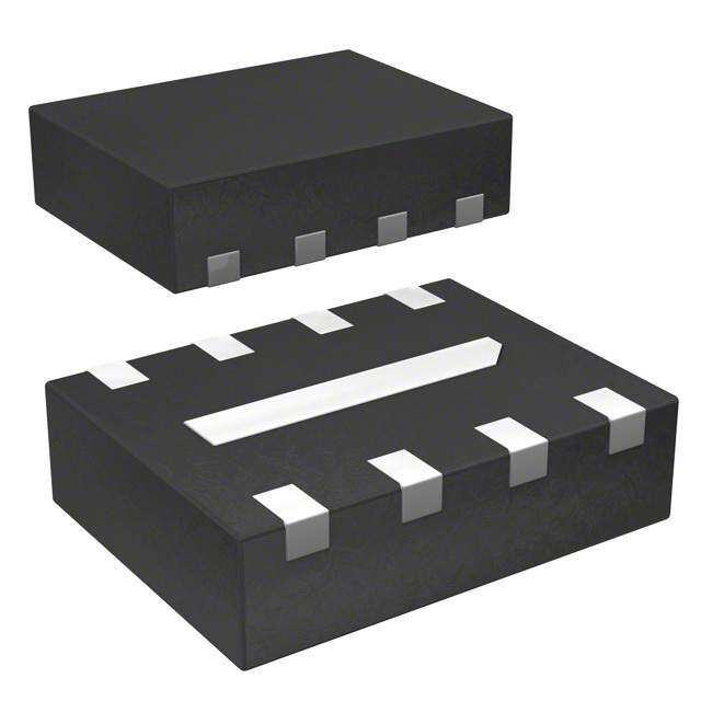
| 描述 | IC RMS POWER DETECTOR 8-DFN |
| 产品分类 | |
| 品牌 | Linear Technology |
| 数据手册 | http://www.linear.com/docs/26614 |
| 产品图片 |
|
| 产品型号 | LT5581IDDB#TRMPBF |
| RF类型 | CATV |
| rohs | 无铅 / 符合限制有害物质指令(RoHS)规范要求 |
| 产品系列 | - |
| 产品目录页面 | |
| 其它名称 | LT5581IDDB#TRMPBFDKR |
| 包装 | Digi-Reel® |
| 封装/外壳 | 8-WFDFN 裸露焊盘 |
| 标准包装 | 1 |
| 电压-电源 | 2.7 V ~ 5.25 V |
| 电流-电源 | 1.4mA |
| 精度 | ±1dB |
| 输入范围 | -34dBm ~ 6dBm |
| 频率 | 10MHz ~ 6GHz |


- 商务部:美国ITC正式对集成电路等产品启动337调查
- 曝三星4nm工艺存在良率问题 高通将骁龙8 Gen1或转产台积电
- 太阳诱电将投资9.5亿元在常州建新厂生产MLCC 预计2023年完工
- 英特尔发布欧洲新工厂建设计划 深化IDM 2.0 战略
- 台积电先进制程称霸业界 有大客户加持明年业绩稳了
- 达到5530亿美元!SIA预计今年全球半导体销售额将创下新高
- 英特尔拟将自动驾驶子公司Mobileye上市 估值或超500亿美元
- 三星加码芯片和SET,合并消费电子和移动部门,撤换高东真等 CEO
- 三星电子宣布重大人事变动 还合并消费电子和移动部门
- 海关总署:前11个月进口集成电路产品价值2.52万亿元 增长14.8%


PDF Datasheet 数据手册内容提取
LT5581 6GHz RMS Power Detector with 40dB Dynamic Range FEATURES DESCRIPTION n Frequency Range: 10MHz to 6GHz The LT®5581 is a 10MHz to 6GHz, low power monolithic n Accurate Power Measurement of High Crest Factor precision RMS power detector. The RMS detector uses a (Up to 12dB) Waveforms proprietary technique to accurately measure the RF power n 40dB Log Linear Dynamic Range from –34dBm to +6dBm (at 2.14GHz) of modulated signals n Exceptional Accuracy Over Temperature with a crest factor as high as 12dB. It outputs a DC voltage n Fast Response Time: 1μs Rise, 8μs Fall in linear scale proportional to an RF input signal power n Low Power: 1.4mA at 3.3V in dBm. The LT5581 is suitable for precision power mea- n Log-Linear DC Output vs Input RF Power in dBm surement and control for a wide variety of RF standards, n Small 3mm × 2mm 8-Pin DFN Package including GSM/EDGE, CDMA, CDMA2000, W-CDMA, n Single-Ended RF Input TD-SCDMA, UMTS, LTE and WiMAX, etc. The final DC out- put is connected in series with an on-chip 300Ω resistor, APPLICATIONS which enables further filtering of the output modulation ripple with just a single off-chip capacitor. n GSM/EDGE, CMDA, CDMA2000, W-CDMA, LTE, L, LT, LTC, LTM, Linear Technology and the Linear logo are registered trademarks of Linear WiMAX RF Power Control Technology Corporation. All other trademarks are the property of their respective owners. Protected by U.S. Patents, including 7342431. n Pico-Cells, Femto-Cells RF Power Control n Wireless Repeaters n CATV/DVB Transmitters n MIMO Wireless Access Points n Portable RMS Power Measurement Instrumentation TYPICAL APPLICATION 10MHz to 6GHz Infrastructure Power Linearity Error vs RF Input Power, Amplifier Level Control 2140MHz Modulated Waveforms DIRECTIONAL 3 RFIN POAMWPER COUPLER RFOUT TA = 25°C 2 VCC CMATCH 2.7VDC TO 5.25VDC dB) 0.1µF 0.01µF R ( 1 O CDPOIONGWTITREAORLL 12 VENCC LT5581 RCFSIQN 87 1000pF LMATCH 50Ω EARITY ERR–10 CW ADC 3 VOUT GND 6 LIN WWCCDDMMAA, DULL 1C 68Ω 4 5 –2 WCDMA DL 4C CFILT GND GND GND LTE DL 1C 0.01µF 9 LTE DL 4C –3 5581 TA01a –35 –30 –25 –20 –15 –10 –5 0 5 10 RF INPUT POWER (dBm) 5581 TA01b 5581fb 1 For more information www.linear.com/LT5581
LT5581 ABSOLUTE MAXIMUM RATINGS PIN CONFIGURATION (Note 1) Supply Voltage .........................................................5.5V TOP VIEW Maximum Input Signal Power—Average .............15dBm Maximum Input Signal Power—Peak (Note 7) ....25dBm VCC 1 8 CSQ DC Voltage at RF .......................................–0.3V to 2V EN 2 7 RFIN IN 9 V Voltage ....................................–0.3V to V + 0.3V VOUT 3 6 GND OUT CC GND 4 5 GND Maximum Junction Temperature, T ...............150°C JMAX Operating Temperature Range .................–40°C to 85°C DDB PACKAGE Storage Temperature Range ..................–65°C to 150°C 8-LEAD (3mm × 2mm) PLASTIC DFN TJMAX = 150°C, θJA = 76°C/W EXPOSED PAD (PIN 9) IS GND, MUST BE SOLDERED TO PCB CAUTION: This part is sensitive to electrostatic discharge. It is very important that proper ESD precautions be observed when handling the LT5581. ORDER INFORMATION LEAD FREE FINISH TAPE AND REEL PART MARKING PACKAGE DESCRIPTION TEMPERATURE RANGE LT5581IDDB#PBF LT5581IDDB#TRPBF LDKM 8-Lead (3mm × 2mm) Plastic DFN –40°C to 85°C Consult LTC Marketing for parts specified with wider operating temperature ranges. Consult LTC Marketing for information on non-standard lead based finish parts. For more information on lead free part marking, go to: http://www.linear.com/leadfree/ For more information on tape and reel specifications, go to: http://www.linear.com/tapeandreel/ ELECTRICAL CHARACTERISTICS The l denotes the specifications which apply over the full operating temperature range, otherwise specifications are at T = 25°C, V = 3.3V, EN = 3.3V, unless otherwise noted (Note 2). Test circuit is shown in Figure 1. A CC PARAMETER CONDITIONS MIN TYP MAX UNITS AC Input Input Frequency Range (Note 4) 10-6000 MHz Input Impedance 205||1.6 Ω||pF f = 450MHz RF RF Input Power Range Externally Matched to 50Ω Source –34 to 6 dBm Linear Dynamic Range, CW (Note 3) ±1dB Linearity Error 40 dB Linear Dynamic Range, CDMA (Note 3) ±1dB Linearity Error; CDMA 4-Carrier 40 dB Output Slope 31 mV/dB Logarithmic Intercept (Note 5) –42 dBm Output Variation vs Temperature Normalized to Output at 25˚C, –40°C < T < 85°C; ±1 dB A P = –34 to +6dBm IN Output Variation vs Temperature Normalized to Output at 25°C, –40°C < T < 85°C; ±0.5 dB A P = –27 to –10dBm IN Deviation from CW Response; TETRA π/4 DQPSK ±0.1 dB P = –34dBm to 0dBm CDMA 4-Carrier 64-Channel Fwd 1.23Mcps ±0.5 dB IN 5581fb 2 For more information www.linear.com/LT5581
LT5581 ELECTRICAL CHARACTERISTICS The l denotes the specifications which apply over the full operating temperature range, otherwise specifications are at T = 25°C, V = 3.3V, EN = 3.3V, unless otherwise noted (Note 2). Test circuit is shown in Figure 1. A CC PARAMETER CONDITIONS MIN TYP MAX UNITS 2nd Order Harmonic Distortion At RF Input; CW Input; P = 0dBm –57 dBc IN 3rd Order Harmonic Distortion At RF Input; CW Input; P = 0dBm –52 dBc IN f = 880MHz RF RF Input Power Range Externally Matched to 50Ω Source –34 to 6 dBm Linear Dynamic Range, CW (Note 3) ±1dB Linearity Error 40 dB Linear Dynamic Range, EDGE (Note 3) ±1dB Linearity Error; EDGE 3π/8-Shifted 8PSK 40 dB Output Slope 31 mV/dB Logarithmic Intercept (Note 5) –42 dBm Output Variation vs Temperature Normalized to Output at 25°C, –40°C < T < 85°C; ±1 dB A P = –34 to +6dBm IN Output Variation vs Temperature Normalized to Output at 25°C, –40°C < T < 85°C; ±0.5 dB A P = –27 to –10dBm IN Deviation from CW Response, Pin = –34 to +6dBm EDGE 3π/8 Shifted 8PSK ±0.1 dB f = 2140MHz RF RF Input Power Range Externally Matched to 50Ω Source –34 to 6 dBm Linear Dynamic Range, CW (Note 3) ±1dB Linearity Error 43 dB Linear Dynamic Range, WCDMA (Note 3) ±1dB Linearity Error; 4-Carrier WCDMA 37 dB Output Slope 31 mV/dB Logarithmic Intercept (Note 5) –42 dBm Output Variation vs Temperature Normalized to Output at 25°C, –40°C < T < 85°C; ±1 dB A P = –34 to 6dBm IN Output Variation vs Temperature Normalized to Output at 25°C, –40°C < T < 85°C; ±0.5 dB A P = –27 to –10dBm IN Maximum Deviation from CW Response WCDMA 1-Carrier Uplink ±0.1 dB P = –34 to –4dBm WCDMA 64-Channel 4-Carrier Downlink ±0.5 dB IN f = 2600MHz RF RF Input Power Range Externally Matched to 50Ω Source –34 to 6 dBm Linear Dynamic Range, CW (Note 3) ±1dB Linearity Error 40 dB Output Slope 31 mV/dB Logarithmic Intercept (Note 5) –42 dBm Output Variation vs Temperature Normalized to Output at 25°C, –40°C < T < 85°C; ±1 dB A P = –34 to +6dBm IN Output Variation vs Temperature Normalized to Output at 25°C, –40°C < T < 85°C; ±0.5 dB A P = –27 to –10dBm IN Maximum Deviation from CW Response WiMAX OFDMA Preamble ±0.1 dB P = –34 to 2dBm WiMAX OFDM Burst ±0.5 dB IN f = 3500MHz RF RF Input Power Range Externally Matched to 50Ω Source –30 to 6 dBm Linear Dynamic Range, CW (Note 3) ±1dB Linearity Error 36 dB Output Slope 31 mV/dB Logarithmic Intercept (Note 5) –41 dBm Output Variation vs Temperature Normalized to Output at 25°C, –40°C < T < 85°C; ±1 dB A P = –30 to +6dBm IN 5581fb 3 For more information www.linear.com/LT5581
LT5581 ELECTRICAL CHARACTERISTICS The l denotes the specifications which apply over the full operating temperature range, otherwise specifications are at T = 25°C, V = 3.3V, EN = 3.3V, unless otherwise noted (Note 2). Test circuit is shown in Figure 1. A CC PARAMETER CONDITIONS MIN TYP MAX UNITS Output Variation vs Temperature Normalized to Output at 25°C, –40°C < T < 85°C; ±0.5 dB A P = –27 to –10dBm IN Deviation from CW Response WiMAX OFDMA Preamble ±0.1 dB P = –34 to –4dBm WiMAX OFDM Burst ±0.5 dB IN f = 5800MHz RF RF Input Power Range Externally Matched to 50Ω Source –25 to 6 dBm Linear Dynamic Range, CW (Note 3) ±1dB Linearity Error 31 dB Output Slope 31 mV/dB Logarithmic Intercept (Note 5) –33 dBm Output Variation vs Temperature Normalized to Output at 25°C, –40°C < T < 85°C; ±1 dB A P = –25 to +6dBm IN Output Variation vs Temperature Normalized to Output at 25°C, –40°C < T < 85°C; ±0.5 dB A P = –20 to +6dBm IN Deviation from CW Response WiMAX OFDM Burst; P = –25 to 6dBm ±0.2 dB IN Output Output DC Voltage No Signal Applied to RF Input 180 mV Output Impedance Internal Series Resistor Allows for Off-Chip Filter Cap 300 Ω Output Current Sourcing/Sinking 5/5 mA Rise Time 0.2V to 1.6V, 10% to 90%, f = 2140MHz 1 µs RF Fall Time 1.6V to 0.2V, 10% to 90%, f = 2140MHz 8 µs RF Power Supply Rejection Ratio (Note 6) For Over Operating Input Power Range 49 dB Integrated Output Voltage Noise 1kHz to 6.5kHz Integration BW, P = 0dBm CW 150 µV IN RMS Enable (EN) Low = Off, High = On EN Input High Voltage (On) l 2 V EN Input Low Voltage (Off) l 0.3 V Enable Pin Input Current EN = 3.3V 20 µA Turn-On Time; CW RF input V Within 10% of Final Value; P = 0dBm 1 µs OUT IN Settling Time; RF Pulse V Within 10% of Final Value; P = 0dBm 1 µs OUT IN Power Supply Supply Voltage l 2.7 3.3 5.25 V Supply Current No RF Input Signal 1.4 mA Shutdown Current EN = 0.3V, V = 3.3V 0.2 6 µA CC Note 1: Stresses beyond those listed under Absolute Maximum Ratings Note 4: An external capacitor at the C pin should be used for input SQ may cause permanent damage to the device. Exposure to any Absolute frequencies below 250MHz. Lower frequency operation results in Maximum Rating condition for extended periods may affect device excessive RF ripple in the output voltage. reliability and lifetime. Note 5: Logarithmic intercept is an extrapolated input power level from the Note 2: The LT5581 is guaranteed functional over the operating best fitted log-linear straight line, where the output voltage is 0V. temperature range from –40°C to 85°C. Note 6: PSRR is determined as the dB value of the change in V voltage OUT Note 3: The linearity error is calculated by the difference between the over the change in V supply voltage. CC incremental slope of the output and the average output slope from Note 7: Not production tested. Guaranteed by design and correlation to –20dBm to 0dBm. The dynamic range is defined as the range over which production tested parameters. the linearity error is within ±1dB. 5581fb 4 For more information www.linear.com/LT5581
LT5581 TYPICAL PERFORMANCE CHARACTERISTICS Performance characteristics taken at V = 3.3V, CC EN = 3.3V and T = 25°C, unless otherwise noted. (Test circuit shown in Figure 1) A Output Voltage vs Frequency Output Voltage vs Frequency Linearity Error vs Frequency 2.0 2.0 3 TA = 25°C TA = 25°C TA = 25°C 1.8 1.8 10MHz 880MHz 2 1.6 450MHz 1.6 2.14GHz 1.4 880MHz 1.4 2.6GHz dB) 2.14GHz 3.5GHz R ( 1 1.2 2.6GHz 1.2 O V (V)OUT10..08 35..58GGHHzz V (V)OUT10..08 RITY ERR 0 10MHz EA–1 450MHz 0.6 0.6 LIN 880MHz 2.14GHz 0.4 0.4 –2 2.6GHz 0.2 0.2 3.5GHz 5.8GHz 0 0 –3 –40–35–30–25–20–15–10 –5 0 5 10 –40–35–30–25–20–15–10 –5 0 5 10 –40–35–30–25–20–15–10 –5 0 5 10 RF INPUT POWER (dBm) RF INPUT POWER (dBm) RF INPUT POWER (dBm) 5581 G01 5581 G02 5581 G03 Output Voltage and Linearity Error Linearity Error Temperature Linearity Error vs RF Input Power, at 450MHz Variation from 25°C at 450MHz 450MHz Modulated Waveforms 2.0 2.5 3 3 25°C TA = 25°C 1.8 85°C 2.0 –40°C 2 2 CW 1.6 1.5 TETRA 1.4 1.0 LINEA B) 1 85°C R(dB) 1 CDMA 4C V (V)OUT101...082 –000.5.5 RITY ERRO RIATION (d 0 –40°C RITY ERRO 0 0.6 –1.0 R (d VA–1 NEA–1 B) LI 0.4 –1.5 –2 –2 0.2 –2.0 0 –2.5 –3 –3 –40–35–30–25–20–15–10 –5 0 5 10 –40–35–30–25–20–15–10 –5 0 5 10 –35 –30 –25 –20 –15 –10 –5 0 5 10 RF INPUT POWER (dBm) RF INPUT POWER (dBm) RF INPUT POWER (dBm) 5581 G04 5581 G05 5581 G06 Output Voltage and Linearity Error Linearity Error Temperature Linearity Error vs RF Input Power, at 880MHz Variation from 25°C at 880MHz 880MHz Modulated Waveforms 2.0 2.5 3 3 25°C TA = 25°C 1.8 85°C 2.0 –40°C 2 2 CW 1.6 1.5 EDGE 1.4 1.0 LINEA B) 1 85°C R(dB) 1 1.2 0.5 R d O V (V)OUT10..08 –00.5 ITY ERRO RIATION ( 0 –40°C RITY ERR 0 0.6 –1.0 R (dB) VA–1 LINEA–1 0.4 –1.5 –2 –2 0.2 –2.0 0 –2.5 –3 –3 –40–35–30–25–20–15–10 –5 0 5 10 –40–35–30–25–20–15–10 –5 0 5 10 –35 –30 –25 –20 –15 –10 –5 0 5 10 RF INPUT POWER (dBm) RF INPUT POWER (dBm) RF INPUT POWER (dBm) 5581 G07 5581 G08 5581 G09 5581fb 5 For more information www.linear.com/LT5581
LT5581 TYPICAL PERFORMANCE CHARACTERISTICS Output Voltage and Linearity Error Linearity Error Temperature Linearity Error vs RF Input Power, at 2140MHz Variation from 25°C at 2140MHz 2140MHz Modulated Waveforms 2.0 2.5 3 3 25°C TA = 25°C 1.8 85°C 2.0 –40°C 2 2 1.6 1.5 V (V)OUT10101.....08462 –1–00.1.005..05 LINEARITY ERROR (dB VARIATION (dB)–110 –8450°°CC NEARITY ERROR (dB)–110 CWWCDMA, UL 0.4 –1.5 ) LI WCDMA DL 1C –2 –2 WCDMA DL 4C 0.2 –2.0 LTE DL 1C LTE DL 4C 0 –2.5 –3 –3 –40–35–30–25–20–15–10 –5 0 5 10 –40–35–30–25–20–15–10 –5 0 5 10 –35 –30 –25 –20 –15 –10 –5 0 5 10 RF INPUT POWER (dBm) RF INPUT POWER (dBm) RF INPUT POWER (dBm) 5581 G10 5581 G11 5581 G12 Output Voltage and Linearity Error Linearity Error Temperature Linearity Error vs RF Input Power, at 2600MHz Variation from 25°C at 2600MHz 2.6GHz Modulated Waveforms 2.0 2.5 3 3 25°C TA = 25°C 1.8 85°C 2.0 –40°C 2 2 1.6 1.5 V (V)OUT10101.....08462 –1–00.1.005..05 LINEARITY ERROR (dB VARIATION (dB)–110 –8450°°CC NEARITY ERROR (dB)–110 ) LI 0.4 –1.5 CW –2 –2 WiMax OFDM PREAMBLE 0.2 –2.0 WiMax OFDM BURST 0 –2.5 –3 –3 WiMax OFDMA PREAMBLE –40–35–30–25–20–15–10 –5 0 5 10 –40–35–30–25–20–15–10 –5 0 5 10 –35 –30 –25 –20 –15 –10 –5 0 5 10 RF INPUT POWER (dBm) RF INPUT POWER (dBm) RF INPUT POWER (dBm) 5581 G13 5581 G14 5581 G15 Output Voltage and Linearity Error Linearity Error Temperature Linearity Error vs RF Input Power, at 3500MHz Variation from 25°C at 3500MHz 3.5GHz Modulated Waveforms 2.0 2.5 3 3 25°C TA = 25°C 1.8 85°C 2.0 –40°C 2 2 1.6 1.5 V (V)OUT10101.....08462 –1–00.1.005..05 LINEARITY ERROR (dB) VARIATION (dB)–110 –8450°°CC LINEARITY ERROR (dB)–110 0.4 –1.5 –2 –2 CW 0.2 –2.0 WiMax OFDMA PREAMBLE WiMax OFDM BURST 0 –2.5 –3 –3 –40–35–30–25–20–15–10 –5 0 5 10 –40–35–30–25–20–15–10 –5 0 5 10 –35 –30 –25 –20 –15 –10 –5 0 5 10 RF INPUT POWER (dBm) RF INPUT POWER (dBm) RF INPUT POWER (dBm) 5581 G16 5581 G17 5581 G18 5581fb 6 For more information www.linear.com/LT5581
LT5581 TYPICAL PERFORMANCE CHARACTERISTICS Output Voltage and Linearity Error Linearity Error Temperature Linearity Error vs RF Input Power, at 5800MHz Variation from 25°C at 5800MHz 5.8GHz Modulated Waveforms 2.0 2.5 3 3 25°C TA = 25°C 1.8 85°C 2.0 –40°C 2 2 1.6 1.5 V (V)OUT10101.....08462 –1–00.1.005..05 LINEARITY ERROR (dB) VARIATION (dB)–110 –8450°°CC LINEARITY ERROR (dB)–110 0.4 –1.5 –2 –2 0.2 –2.0 CW WiMax OFDM BURST 0 –2.5 –3 –3 –40–35–30–25–20–15–10 –5 0 5 10 –40–35–30–25–20–15–10 –5 0 5 10 –35 –30 –25 –20 –15 –10 –5 0 5 10 RF INPUT POWER (dBm) RF INPUT POWER (dBm) RF INPUT POWER (dBm) 5581 G19 5581 G20 5581 G21 Slope vs Frequency Slope Distribution vs Temperature Supply Current vs Supply Voltage 34 50 2.0 TA = 25°C TA = 85°C TA = 25°C 40 TA = –40°C 1.8 32 A) 85°C dB) N (%) 30 NT (m 1.6 25°C SLOPE (mV/ 30 DISTRIBUTIO 20 PPLY CURRE 11..42 –40°C U 28 S 10 1.0 26 0 0.8 0 1 2 3 4 5 6 28 29 30 31 32 33 34 2.6 3 3.4 3.8 4.2 4.6 5 5.4 FREQUENCY (GHz) SLOPE (mV/dB) SUPPLY VOLTAGE (V) 5581 G22 5581 G23 5581 G24 Logarithmic Intercept Logarithmic Intercept Distribution vs Frequency vs Temperature –30 50 TA = 25°C TA = 85°C TA = 25°C m) 40 TA = –40°C B d–35 PT ( %) CE N ( 30 R O NTE–40 UTI MIC I TRIB 20 TH DIS RI A–45 G 10 O L –50 0 0 1 2 3 4 5 6 –48 –47 –46 –45 –44 –43 –42 –41 FREQUENCY (GHz) LOGARITHMIC INTERCEPT (dBm) 5581 G25 5581 G26 5581fb 7 For more information www.linear.com/LT5581
LT5581 TYPICAL PERFORMANCE CHARACTERISTICS Output Voltage and Linearity Error Supply Current vs RF Input Power vs V at 2140MHz CC 16 2.0 2.5 TA = 25°C TA = 25°C 1.8 2.0 14 3.3V 1.6 5V 1.5 mA) 12 1.4 1.0 LIN SUPPLY CURRENT ( 18604 V (V)OUT1001....0862 ––001.05..05 EARITY ERROR (dB) 0.4 –1.5 2 0.2 –2.0 0 0 –2.5 –25 –20 –15 –10 –5 0 5 10 15 –40–35–30–25–20–15–10 –5 0 5 10 RF INPUT POWER (dBm) RF INPUT POWER (dBm) 5581 G28 5581 G27 Return Loss vs Frequency Output Transient Response with Reference in Figure 1 Test Circuit RF and EN Pulse 0 3.0 10 TA = 25°C TA = 25°C, VCC = 5V 2.5 RF & EN RF & EN 5 –5 PULSE PULSE RF & EN PULSE ON RETURN LOSS (dB)–––211050 OUTPUT VOLTAGE (V)1102....5050 OFF PPPPPIIINNNININ ==== = –––1 01230d000dBdddBBBBmmmmm OFF –––051105 RF PULSE ENABLE (V ) –25 0 –20 –30 –0.5 –25 0 1 2 3 4 5 6 0 0.1 0.2 0.3 0.4 0.5 0.6 0.7 0.8 0.9 1 FREQUENCY (GHz) TIME (ms) L1, C1 = 2.2nH, 1.5pF L1, C1 = 0nH, 0.5pF 5581 G30 L1, C1 = 1nH, 1.5pF L1, C1 = 0nH, 0pF L1, C1 = 0nH, 1pF 5581 G29 Output Transient Response with Output Transient Response CW RF and EN Pulse 3.0 10 3.0 4 TA = 25°C, VCC = 5V TA = 25°C RF RF PULSE ON RF 2.5 EN EN PULSE ON EN 2 2.5 PULSE PULSE 5 PULSE PULSE UT VOLTAGE (V)12..50 OFF PPININ = = 1 00ddBBmm OFF –05 RF PULSE ENAB UT VOLTAGE (V)112...500 OFF PPPINININ == = –1 010d0dBdBBmmm OFF ––024 ENABLE (V OUTP1.0 PPIINN == ––1200ddBBmm –10 LE (V) OUTP0.5 PPIINN == ––2300ddBBmm –6 ) 0.5 PIN = –30dBm –15 0 –8 0 –20 –0.5 –10 0 10 20 30 40 50 60 70 80 90 100 0 0.1 0.2 0.3 0.4 0.5 0.6 0.7 0.8 0.9 1 TIME (µs) TIME (ms) 5581 G31 5581 G32 5581fb 8 For more information www.linear.com/LT5581
LT5581 PIN FUNCTIONS V (Pin 1): Power Supply, 2.7V to 5.25V. V C (Pin 8): Optional Low Frequency Range Extension CC CC SQ should be bypassed with a 0.1µF ceramic capacitor. Capacitor. This pin is for frequencies below 250MHz. Use 0.01µF from pin to ground for 10MHz operation. EN (Pin 2): Chip Enable. A logic low or no-connect on the enable pin shuts down the part. A logic high enables the Exposed Pad (Pin 9): Ground. The Exposed Pad must part. An internal 500k pull-down resistor ensures the part be soldered to the PCB. For high frequency operation, is off when the enable driver is in a three-state condition. the backside ground connection should have a low inductance connection to the PCB ground, using many V (Pin 3): Detector Output. OUT through-hole vias. See the layout information in the GND (Pins 4, 5, 6): Ground. Applications Information section. RF (Pin 7): RF Input. Should be DC-blocked with coupling IN capacitor; 1000pF recommended. This pin has an internal 200Ω termination. BLOCK DIAGRAM 9 LT5581 EXPOSED PAD OUTPUT BUFFER 150kHz LPF RFIN RMS 300Ω VOUT 7 3 DETECTOR BIAS GND CSQ EN VCC 8 2 1 4 5 6 5581 BD 5581fb 9 For more information www.linear.com/LT5581
LT5581 TEST CIRCUIT C7 0.1µF VCC C6 100pF C3 0.01µF 1 8 C5 EN VCC CSQ C2 L1 OPT 1000pF 2.2nH RFIN 2 7 EN LT5581 RFIN VOUT R3 R2 C1 0Ω 3 6 68Ω 1.5pF VOUT GND NC C4 OPT 4 5 NC GND GND GND NC 9 PINS 4, 5, 6: OPTIONAL GROUND 5581 F01 RF 0.018" EE = 4.4 GND 0.062" DC 0.018" GND REF DES VALUE SIZE PART NUMBER RF MATCH FREQUENCY IN C6 100pF 0603 AVX 06033A101KAT2A RANGE L1 C1 C7 0.1µF 0603 AVX 06033C104KAT2A 1GHz to 2.2GHz 2.2nH 1.5pF C3 0.01µF 0603 AVX 06033C103KAT2A 2GHz to 2.6GHz 1.2nH 1.5pF C2 1000pF 0603 AVX 06033C102KAT2A 2.6GHz to 3.4GHz 0 1pF R2 68Ω 0603 3.8GHz to 5.5GHz 0 0.5pF 4.6GHz to 6GHz 0 0 Figure 1. Evaluation Circuit Schematic 5581fb 10 For more information www.linear.com/LT5581
LT5581 APPLICATIONS INFORMATION OPERATION Table 1. RF Input Impedance To achieve an accurate average power measurement of INPUT S11 FREQUENCY IMPEDANCE the high crest factor modulated RF signals, the LT5581 (MHz) (Ω) MAG ANGLE (°) combines a proprietary high speed power measurement 10 203.6-j5.5 0.606 –0.8 subsystem with an internal 150kHz low pass averaging 50 199.5-j22.4 0.603 –3.4 filter and an output voltage buffer in a completely integrated 100 191.7-j40.3 0.601 –6.4 solution with minimal off-chip components. The resulting 200 171.1-j68.5 0.601 –12.3 output voltage is directly proportional to the average RF 400 121.8-j95.4 0.608 –24 input power in dBm. Figure 1 shows the evaluation circuit 500 100.2-j97.5 0.613 –29.8 schematic, and Figures 2 and 3 show the associated board artwork. For best high frequency performance, it is import- 800 56.8-j86.5 0.631 –46.5 ant to place many ground vias directly under the package. 900 48-j81.2 0.638 –51.8 1000 41.1-j76 0.645 –56.8 RF Input Matching 1500 22.2-j55 0.679 –79.5 The input resistance is about 205Ω. Input capacitance 2000 14.6-j41.4 0.710 –97.9 is 1.6pF. The impedance vs frequency of the RF input is 2100 13.6-j39.2 0.716 –101.2 detailed in Table 1. 2500 10.8-j32.1 0.737 –112.9 3000 8.6-j25 0.759 –125.7 3500 7.3-j19.4 0.774 –136.9 4000 6.6-j14.5 0.783 –147.1 5000 8.8-j9.6 0.709 –157.6 6000 6.4-j0 0.774 –179.9 5581 F02 5581 F03 Figure 2. Top Side of Evaluation Board Figure 3. Bottom Side of Evaluation Board 5581fb 11 For more information www.linear.com/LT5581
LT5581 APPLICATIONS INFORMATION A shunt 68Ω resistor can be used to provide a broadband frequency operation. For input frequencies down to 10MHz, impedance match at low frequencies up to 1.3GHz, and 0.01µF is needed at C . For frequencies above 250MHz, SQ from 4.5GHz to 6GHz. As shown in Figure 4, a nominal the on-chip 20pF decoupling capacitor is sufficient, and C SQ broadband input match can be achieved up to 2.2GHz by may be eliminated as desired. The DC-blocking capacitor using an LC matching circuit consisting of a series 2.2nH can be as large as 2200pF for 10MHz operation, or 100pF inductor (L1) and a shunt 1.5pF capacitor (C1). This for 2GHz operation. A DC-blocking capacitor larger than match will maintain a return loss of about 10dB across 2200pF results in an undesirable RF pulse response on the band. For matching at higher frequencies, values for the falling edge. Therefore, for general applications, the L1 and C1 are listed in the table of Figure 1. The input recommended value for C2, is conservatively set at 1000pF. reflection coefficient referenced to the RF input pin (with no external components) is shown on the Smith Chart Output Interface in Figure 5. Alternatively, it is possible to match using The output buffer of the LT5581 is shown in Figure 6. It an impedance transformation network by omitting R1 includes a push-pull stage with a series 300Ω resistor. and transforming the 205Ω load to 50Ω. The resulting The output stage is capable of sourcing and sinking 5mA match, over a narrow band of frequencies, will improve of current. The output pin can be shorted to GND or V CC sensitivity up to about 6dB maximum; the dynamic range without damage, but going beyond V + 0.5V or GND – CC remains the same. For example, by omitting R1 and 0.5V may result in damage, as the internal ESD protection setting L1 = 1.8nH and C1 = 3pF, a 2:1 VSWR match can diodes will start to conduct excessive current. be obtained from 1.95GHz to 2.36GHz, with a sensitivity The residual ripple, due to RF modulation, can be reduced improvement of 5dB. by adding external components R and C (R3 and SS LOAD The RF input DC blocking capacitor (C2) and the C C4 on the Evaluation Circuit Schematic in Figure 1) to IN SQ bias decoupling capacitor (C3), can be adjusted for low VCC LT5581 C3 0.01µF CSQ 8 20pF 205Ω RFIN C2 (MATCHED) 1000pF L1 RFIN 7 C1 R1 68Ω 5581 F04 Figure 4. Simplified Circuit Schematic of the RF Input Interface Figure 5. Input Reflection Coefficient 5581fb 12 For more information www.linear.com/LT5581
LT5581 APPLICATIONS INFORMATION the output pin, to form an RC lowpass filter. The internal factor of 3, using a 0.047µF external filter capacitor. The 300Ω resistor in series with the output pin enables filter- average power in the preamble section is –10dBm, while ing of the output signal with just the addition of C . the burst section has a 3dB lower average power. With LOAD Figure 7 shows the effect of the external filter capacitor the capacitor, the ripple in the preamble section is about on the residual ripple level for a 4-carrier WCDMA signal 0.5dB peak-to-peak. The modulation used was OFDM at 2.14GHz with –10dBm. Adding a 10nF capacitor to the (WiMAX 802.16-2004) MMDS band, 1.5MHz BW, with output decreases the peak-to-peak output ripple from 256 size FFT and 1 burst at QPSK3/4. 135mV to 50mV . The filter –3dB corner frequency P-P P-P Figure 9 shows how the peak-to-peak ripple decreases with can be calculated with the following equation: increasing external filter capacitance value. Also shown is 1 f = how the RF pulse response will have longer rise and fall C 2πC (300+R ) LOAD SS times with the addition of this lowpass filter cap. Figure 8 shows the transient response for a 2.6GHz Wi- MAX signal, with preamble and burst ripple reduced by a 1.4 1.25 LT5581 VCC TA = 25°C 1.2 NO CAP 1.20 0.01µF INPUT 40µA 300Ω VOUT3 RSS (VFOILUTTERED) OUTPUT VOLTAGE (V)0001....8640 1111....10010505OUTPUT VOLTAGE (V) CLOAD 0.2 0.95 5581 F06 00 10 20 30 40 50 60 70 80 90 1000.90 TIME (µs) 5581 F07 Figure 6. Simplified Circuit Schematic of the Output Interface Figure 7. Residual Ripple, Output Transient Response for RF Pulse with WCDMA 4-Carrier Modulation 1.4 9 1000 TA = 25°C NO CAP RIPPLE TA = 25°C 1.2 0.047µF K (dB) 78 RFAISLEL RIS A E OUTPUT VOLTAGE (V)0001....8640 UTPUT RIPPLE PEAK-TO-PE 36254 11000 TIME AND FALL TIME (µs) 0.2 O 1 0 1 0 0.001 0.01 0.1 1 0 0.2 0.4 0.6 0.8 1 1.2 1.4 1.6 1.8 2 EXTERNAL CAPACITOR (µF) TIME (ms) 5581 F09 5581 F08 Figure 8. Residual Ripple for 2.6GHz WiMAX OFDM 802.16-2004 Figure 9. Residual Ripple, Output Transient Times for RF Pulse with WCDMA 4-Carrier Modulation vs External Filter Capacitor C4 5581fb 13 For more information www.linear.com/LT5581
LT5581 APPLICATIONS INFORMATION Figure 10 shows that rise time and fall time are strong measurements in the measurement period). It is important functions of RF input power. Data is taken without the to note that the CF refers to the 150kHz low pass filtered output filter capacitor. envelope of the signal. The error will depend on the sta- tistics and bandwidth of the modulation signal in relation For a given RF modulation type—WCDMA, for example— to the internal 150kHz filter. For example, in the case of the internal 150kHz filter provides nominal filtering of the WCDMA, simulations prove that it is possible to set the residual ripple level. Additional external filtering occurs in external filter capacitor corner frequency at 15kHz and the log domain, which introduces a systematic log error only introduce an error less than 0.1dB. in relation to the signal’s crest factor, as shown in the following equation in dB.1 Figure 11 depicts the output AM modulation ripple as a function of modulation difference frequency for a 2-tone Error|dB = 10 • log (r + (1 – r)10–CF/10) – CF • (r-1) 10 input signal at 2140MHz with –10dBm input power. The Where CF is the crest factor and r is the duty cycle of the resulting deviation in the output voltage of the detector measurement (or number of measurements made at the shows the effect of the internal 150kHz filter. peak envelope, divided by the total number of periodic 1 Steve Murray, “Beware of Spectrum Analyzer Power Averaging Techniques,” Microwaves & RF, Dec. 2006. 9 30 0 TA = 25°C TA = 25°C 8 D ND FALL TIME (µs) 6547 FALL TIME AC RIPPLE (dB) 122550 –––101...550EVIATION OF OUTPU E TIME A 3 OUTPUT 10 –2.0T VOLTAG S 2 E RI RISE TIME 5 –2.5 (d B 1 ) 0 0 –3.0 –30 –25 –20 –15 –10 –5 0 5 0.001 0.01 0.1 1 10 INPUT POWER (dBm) 2-TONE FREQUENCY SEPARATION (MHz) 5581 F10 5581 F11 Figure 10. RF Pulse Response Rise Time Figure 11. Output DC Voltage Deviation and Residual and Fall Time vs RF Input Power Ripple vs 2-Tone Separation Frequency 4.0 2.0 TA = 25°C TA = 25°C 1.8 3.5 0dBm /Hz)MS 3.0 mV)RMS 11..46 –––123000dddBBBmmm AGE (µVR22..50 D NOISE ( 11..02 NO RF INPUT OLT 1.5 ATE 0.8 V R NOISE 1.0 0––d12B00ddmBBmm INTEG 00..46 0.5 –30dBm 0.2 NO RF INPUT 0 0 0.1 1 10 100 1000 0.1 1 10 100 1000 FREQUENCY (kHz) FREQUENCY (kHz) 5581 F12 5581 F13 Figure 12. Output Voltage Noise Density Figure 13. Integrated Output Voltage Noise 5581fb 14 For more information www.linear.com/LT5581
LT5581 APPLICATIONS INFORMATION The output voltage noise density and integrated noise are It is important that the voltage applied to the EN pin never shown in Figures 12 and 13, respectively, for various input exceeds V by more than 0.5V, otherwise, the supply CC power levels. Noise is a strong function of input level. There current may be sourced through the upper ESD protection is roughly a 10dB reduction in the output noise level for diode connected at the EN pin. an input level of 0dBm versus no input. LT5581 VCC Enable Pin A simplified schematic of the EN pin is shown in Figure 14. EN 2 To enable the LT5581, it is necessary to put greater than 500k 300k 300k 2V on this pin. To disable or turn off the chip, this voltage should be below 0.3V. At an enable voltage of 3.3V, the pin draws roughly 20µA. If the EN pin is not connected, the chip is disabled through an internal 500k pull-down resistor. 5581 F14 Figure 14. Enable Pin Simplified Schematic 5581fb 15 For more information www.linear.com/LT5581
LT5581 PACKAGE DESCRIPTION Please refer to http://www.linear.com/designtools/packaging/ for the most recent package drawings. DDB Package 8-Lead Plastic DFN (3mm × 2mm) (Reference LTC DWG # 05-08-1702 Rev B) 0.61 ±0.05 (2 SIDES) 0.70 ±0.05 2.55 ±0.05 1.15 ±0.05 PACKAGE OUTLINE 0.25 ±0.05 0.50 BSC 2.20 ±0.05 (2 SIDES) RECOMMENDED SOLDER PAD PITCH AND DIMENSIONS 3.00 ±0.10 R = 0.115 0.40 ±0.10 R = 0.05 TYP (2 SIDES) TYP 5 8 2.00 ±0.10 PIN 1 BAR (2 SIDES) PIN 1 TOP MARK R = 0.20 OR (SEE NOTE 6) 0.56 ±0.05 0.25 × 45° (2 SIDES) 4 1 CHAMFER (DDB8) DFN 0905 REV B 0.200 REF 0.75 ±0.05 0.25 ±0.05 0.50 BSC 2.15 ±0.05 (2 SIDES) 0 – 0.05 BOTTOM VIEW—EXPOSED PAD NOTE: 1. DRAWING CONFORMS TO VERSION (WECD-1) IN JEDEC PACKAGE OUTLINE M0-229 2. DRAWING NOT TO SCALE 3. ALL DIMENSIONS ARE IN MILLIMETERS 4. DIMENSIONS OF EXPOSED PAD ON BOTTOM OF PACKAGE DO NOT INCLUDE MOLD FLASH. MOLD FLASH, IF PRESENT, SHALL NOT EXCEED 0.15mm ON ANY SIDE 5. EXPOSED PAD SHALL BE SOLDER PLATED 6. SHADED AREA IS ONLY A REFERENCE FOR PIN 1 LOCATION ON THE TOP AND BOTTOM OF PACKAGE 5581fb 16 For more information www.linear.com/LT5581
LT5581 REVISION HISTORY REV DATE DESCRIPTION PAGE NUMBER A 4/10 Updated Note 2 in Electrical Characteristics Section 4 B 8/15 Changed Enable Pin input voltage to 2V 15 5581fb Information furnished by Linear Technology Corporation is believed to be accurate and reliable. 17 However, no responsibility is assumed for its use. Linear Technology Corporation makes no representation that the interconnectionF oofr imts ocirrec uiintsfo arsm daesticornib ewd whewr.eliinn ewailrl. cnoomt in/LfrTin5g5e8 o1n existing patent rights.
LT5581 RELATED PARTS PART NUMBER DESCRIPTION COMMENTS RF Power Detectors LTC®5505 RF Power Detectors with >40dB Dynamic Range 300MHz to 3GHz, Temperature Compensated, 2.7V to 6V Supply LTC5507 100kHz to 1000MHz RF Power Detector 100kHz to 1GHz, Temperature Compensated, 2.7V to 6V Supply LTC5508 300MHz to 7GHz RF Power Detector 44dB Dynamic Range, Temperature Compensated, SC70 Package LTC5509 300MHz to 3GHz RF Power Detector 36dB Dynamic Range, Low Power Consumption, SC70 Package LTC5530 300MHz to 7GHz Precision RF Power Detector Precision V Offset Control, Shutdown, Adjustable Gain OUT LTC5531 300MHz to 7GHz Precision RF Power Detector Precision V Offset Control, Shutdown, Adjustable Offset OUT LTC5532 300MHz to 7GHz Precision RF Power Detector Precision V Offset Control, Adjustable Gain and Offset OUT LT5534 50MHz to 3GHz Log RF Power Detector with ±1dB Output Variation over Temperature, 38ns Response Time, Log Linear Response 60dB Dynamic Range LTC5536 Precision 600MHz to 7GHz RF Power Detector 25ns Response Time, Comparator Reference Input, Latch Enable Input, with Fast Comparator Output –26dBm to +12dBm Input Range LT5537 Wide Dynamic Range Log RF/IF Detector Low Frequency to 1GHz, 83dB Log Linear Dynamic Range LT5538 75dB Dynamic Range 3.8GHz Log RF Power ±0.8dB Accuracy Over Temperature Detector Infrastructure LT5514 Ultralow Distortion, IF Amplifier/ADC Driver 850MHz Bandwidth, 47dBm OIP3 at 100MHz, 10.5dB to 33dB Gain Control Range with Digitally Controlled Gain LT5517 40MHz to 900MHz Quadrature Demodulator 21dBm IIP3, Integrated LO Quadrature Generator LT5519 0.7GHz to 1.4GHz High Linearity Upconverting 17.1dBm IIP3 at 1GHz, Integrated RF Output Transformer with 50Ω Matching, Mixer Single-Ended LO and RF Ports Operation LT5520 1.3GHz to 2.3GHz High Linearity Upconverting 15.9dBm IIP3 at 1.9GHz, Integrated RF Output Transformer with 50Ω Matching, Mixer Single-Ended LO and RF Ports Operation LT5521 10MHz to 3700MHz High Linearity 24.2dBm IIP3 at 1.95GHz, NF = 12.5dB, 3.15V to 5.25V Supply, Single-Ended LO Upconverting Mixer Port Operation LT5522 600MHz to 2.7GHz High Signal Level 4.5V to 5.25V Supply, 25dBm IIP3 at 900MHz, NF = 12.5dB, 50Ω Single-Ended RF Downconverting Mixer and LO Ports LT5525 High Linearity, Low Power Downconverting Single-Ended 50Ω RF and LO Ports, 17.6dBm IIP3 at 1900MHz, I = 28mA CC Mixer LT5526 High Linearity, Low Power Downconverting 3V to 5.3V Supply, 16.5dBm IIP3, 100kHz to 2GHz RF, NF = 11dB, I = 28mA, CC Mixer –65dBm LO-RF Leakage LT5527 400MHz to 3.7GHz High Signal Level IIP3 = 23.5dBm and NF = 12.5dBm at 1900MHz, 4.5V to 5.25V Supply, I = 78mA, CC Downconverting Mixer Conversion Gain = 2dB LT5557 400MHz to 3.8GHz, 3.3V High Signal Level IIP3 = 23.7dBm at 2600MHz, 23.5dBm at 3600MHz, I = 82mA at 3.3V CC Downconverting Mixer LT5560 Ultralow Power Active Mixer 10mA Supply Current, 10dBm IIP3, 10dB NF, Usable as Up- or Down-Converter. LT5568 700MHz to 1050MHz High Linearity Direct 22.9dBm OIP3 at 850MHz, –160.3dBm/Hz Noise Floor, 50Ω, 0.5V Baseband DC Quadrature Modulator Interface, 3-Ch CDMA2000 ACPR = –71.4dBc at 850MHz LT5572 1.5GHz to 2.5GHz High Linearity Direct 21.6dBm OIP3 at 2GHz, –158.6dBm/Hz Noise Floor, High-Ohmic 0.5V Baseband DC Quadrature Modulator Interface, 4-Ch W-CDMA ACPR = –67.7dBc at 2.14GHz LT5575 800MHz to 2.7GHz High Linearity Direct 50Ω, Single-Ended RF and LO Inputs. 28dBm IIP3 at 900MHz, 13.2dBm P1dB, Conversion I/Q Demodulator 0.04dB I/Q Gain Mismatch, 0.4° I/Q Phase Mismatch 5581fb 18 Linear Technology Corporation LT 0815 REV B • PRINTED IN USA 1630 McCarthy Blvd., Milpitas, CA 95035-7417 For more information www.linear.com/LT5581 (408) 432-1900 ● FAX: (408) 434-0507 ● www.linear.com/LT5581 LINEAR TECHNOLOGY CORPORATION 2008
Mouser Electronics Authorized Distributor Click to View Pricing, Inventory, Delivery & Lifecycle Information: A nalog Devices Inc.: LT5581IDDB#PBF LT5581IDDB#TRPBF LT5581IDDB#TRMPBF