ICGOO在线商城 > 射频/IF 和 RFID > RF 混频器 > LT5560EDD#PBF

 Datasheet下载
- 型号: LT5560EDD#PBF
- 制造商: LINEAR TECHNOLOGY
- 库位|库存: xxxx|xxxx
- 要求:
| 数量阶梯 | 香港交货 | 国内含税 |
| +xxxx | $xxxx | ¥xxxx |
查看当月历史价格
查看今年历史价格
LT5560EDD#PBF产品简介:
ICGOO电子元器件商城为您提供LT5560EDD#PBF由LINEAR TECHNOLOGY设计生产,在icgoo商城现货销售,并且可以通过原厂、代理商等渠道进行代购。 LT5560EDD#PBF价格参考。LINEAR TECHNOLOGYLT5560EDD#PBF封装/规格:RF 混频器, RF Mixer IC CATV, DBS, PHS, UHF, VHF Up/Down Converter 10kHz ~ 4GHz 8-DFN (3x3)。您可以下载LT5560EDD#PBF参考资料、Datasheet数据手册功能说明书,资料中有LT5560EDD#PBF 详细功能的应用电路图电压和使用方法及教程。
| 参数 | 数值 |
| 产品目录 | |
| 描述 | IC MIXER 10MHZ-4GHZ UP/DWN 8DFN |
| 产品分类 | |
| 品牌 | Linear Technology |
| 数据手册 | http://www.linear.com/docs/14638 |
| 产品图片 |
|
| 产品型号 | LT5560EDD#PBF |
| RF类型 | CATV,DBS,PHS,UHF,VHF |
| rohs | 无铅 / 符合限制有害物质指令(RoHS)规范要求 |
| 产品系列 | LT5560 |
| 产品目录页面 | |
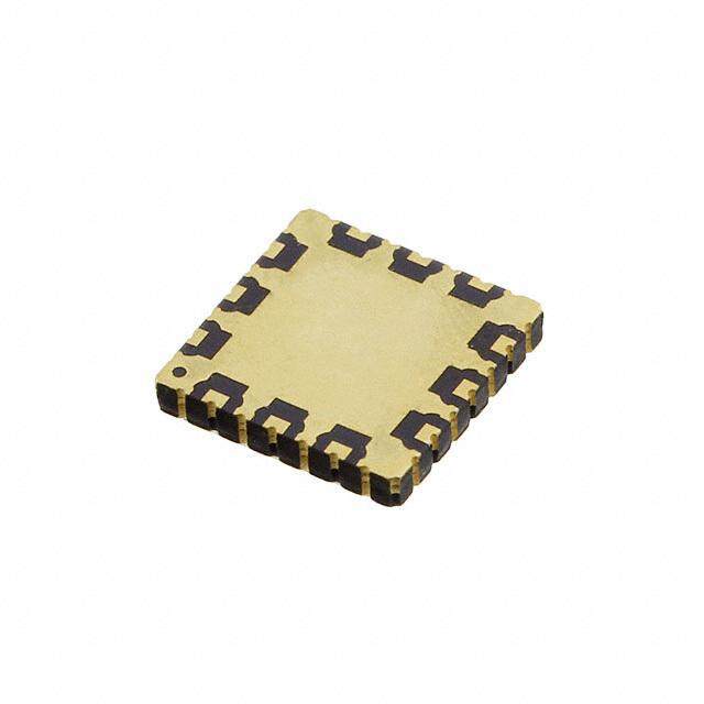
| 供应商器件封装 | 8-DFN(3x3) |
| 其它名称 | LT5560EDDPBF |
| 包装 | 管件 |
| 噪声系数 | 9.3dB |
| 增益 | 2.4dB |
| 封装/外壳 | 8-WFDFN 裸露焊盘 |
| 标准包装 | 121 |
| 混频器数 | 1 |
| 电压-电源 | 2.7 V ~ 5.3 V |
| 电流-电源 | 12mA |
| 辅助属性 | 升/降频器 |
| 频率 | 10kHz ~ 4GHz |


- 商务部:美国ITC正式对集成电路等产品启动337调查
- 曝三星4nm工艺存在良率问题 高通将骁龙8 Gen1或转产台积电
- 太阳诱电将投资9.5亿元在常州建新厂生产MLCC 预计2023年完工
- 英特尔发布欧洲新工厂建设计划 深化IDM 2.0 战略
- 台积电先进制程称霸业界 有大客户加持明年业绩稳了
- 达到5530亿美元!SIA预计今年全球半导体销售额将创下新高
- 英特尔拟将自动驾驶子公司Mobileye上市 估值或超500亿美元
- 三星加码芯片和SET,合并消费电子和移动部门,撤换高东真等 CEO
- 三星电子宣布重大人事变动 还合并消费电子和移动部门
- 海关总署:前11个月进口集成电路产品价值2.52万亿元 增长14.8%


PDF Datasheet 数据手册内容提取
LT5560 0.01MHz to 4GHz Low Power Active Mixer FEATURES DESCRIPTIOU ■ Up or Downconverting Applications The LT®5560 is a low power, high performance broad- ■ Noise Figure: 9.3dB Typical at 900MHz Output band active mixer. This double-balanced mixer can be ■ Conversion Gain: 2.4dB Typical driven by a single-ended LO source and requires only ■ IIP3: 9dBm Typical at ICC = 10mA –2dBm of LO power. The balanced design results in ■ Adjustable Supply Current: 4mA to 13.4mA low LO leakage to the output, while the integrated input ■ Low LO Drive Level: –2dBm amplifi er provides excellent LO to IN isolation. The sig- ■ Single-Ended or Differential LO nal ports can be impedance matched to a broad range ■ High Port-to-Port Isolation of frequencies, which allows the LT5560 to be used as ■ Enable Control with Low Off-State Leakage Current an up- or down-conversion mixer in a wide variety of ■ Single 2.7V to 5V Supply applications. ■ Small 3mm × 3mm DFN Package The LT5560 is characterized with a supply current of 10mA; APPLICATIOUS however, the DC current is adjustable, which allows the performance to be optimized for each application with a ■ Portable Wireless single resistor. For example, when biased at its maximum ■ CATV/DBS Receivers supply current (13.4mA), the typical upconverting mixer ■ WiMAX Radios IIP3 is +10.8dBm for a 900MHz output. ■ PHS Basestations , LT, LTC and LTM are registered trademarks of Linear Technology Corporation. ■ RF Instrumentation All other trademarks are the property of their respective owners. ■ Microwave Data Links ■ VHF/UHF 2-Way Radios TYPICAL APPLICATIOU Low Cost 900MHz Downconverting Mixer 2.7V TO 5.3V IF and IM3 Levels 76L0OMINHz 1µF vOsU TRF Input Power 10 1nF 0 IFOUT 100pF 100pF ne)–10 o 15nH m/T–20 B 1 LO– LO+ 8 EL (d–30 EV–40 4.7pFEN 2 EN U1 VCC 7 2704n.7HpF 27303npHF14IF0OMUHTz POWER L––6500 IM3 TVAC C= =2 53°VC 90R0FMINHz 100pF 6.8nH4.7pF 43 IINN+– LT5560 OOUUTT+– 65 270nH ––8700–20–18–16–14–12–10 –8 –Iff6CLIFOC = ==– 1 47146300.M3–Mm2HHAzz0 PGND RF INPUT POWER (dBm) 9 15nH 6.8nH 4.7pF 5560 TA02 5560 TA01 5560f 1
LT5560 ABSOLUTE WAXIWUW RATIUGS PACKAGE/ORDER IUFORWATIOU (Note 1) Supply Voltage .........................................................5.5V TOP VIEW Enable Voltage ................................–0.3V to V + 0.3V CC LO– 1 8 LO+ LO Input Power (Differential) .............................+10dBm EN 2 7 VCC Input Signal Power (Differential) ........................+10dBm IN+ 3 9 6 OUT+ IN+, IN– DC Currents ..............................................10mA IN– 4 5 OUT– OUT+, OUT– DC Current .........................................10mA T ....................................................................125°C DD PACKAGE JMAX 8-LEAD (3mm × 3mm) PLASTIC DFN Operating Temperature Range .................–40°C to 85°C TJMAX = 125°C, θJA = 43°C/W EXPOSED PAD (PIN 9) IS GND Storage Temperature Range ...................–65°C to 125°C MUST BE SOLDERED TO PCB ORDER PART NUMBER DD PART MARKING LT5560EDD LCBX Order Options Tape and Reel: Add #TR Lead Free: Add #PBF Lead Free Tape and Reel: Add #TRPBF Lead Free Part Marking: http://www.linear.com/leadfree/ Consult LTC Marketing for parts specifi ed with wider operating temperature ranges. DC ELECTRICAL CHARACTERISTICS V = 3V, EN = 3V, T = 25°C, unless otherwise noted. Test circuit CC A shown in Figure 1. (Note 3) PARAMETER CONDITIONS MIN TYP MAX UNITS Power Supply Requirements (V ) CC Supply Voltage 2.7 3 5.3 V Supply Current VCC = 3V, R1 = 3Ω 10 12 mA Shutdown Current EN = 0.3V, V = 3V 0.1 10 µA CC Enable (EN) Low = Off, High = On EN Input High Voltage (On) 2 V EN Input Low Voltage (Off) 0.3 V Enable Pin Input Current EN = 3V 25 µA EN = 0.3V 0.1 µA Turn On Time 2 µs Turn Off Time 5 µs AC ELECTRICAL CHARACTERISTICS (Notes 2 and 3) PARAMETER CONDITIONS MIN TYP MAX UNITS Signal Input Frequency Range (Note 4) Requires External Matching < 4000 MHz LO Input Frequency Range (Note 4) Requires External Matching < 4000 MHz Signal Output Frequency Range (Note 4) Requires External Matching < 4000 MHz 5560f 2
LT5560 AC ELECTRICAL CHARACTERISTICS V = 3V, EN = 3V, T = 25°C, P = –20dBm (–20dBm/tone for 2-tone CC A IN IIP3 tests, Δf = 1MHz), PLO = –2dBm, unless otherwise noted. Test circuits are shown in Figures 1, 2 and 3. (Notes 2 and 3) PARAMETER CONDITIONS MIN TYP MAX UNITS Signal Input Return Loss Z = 50Ω, External Match 15 dB LO Input Return Loss Z = 50Ω, External Match 15 dB Signal Output Return Loss Z = 50Ω, External Match 15 dB LO Input Power –6 to 1 dBm Upconverting Mixer Confi guration: VCC = 3V, EN = 3V, TA = 25°C, PIN = –20dBm (–20dBm/tone for 2-tone IIP3 tests, Δf = 1MHz), PLO = –2dBm, unless otherwise noted. High side LO for 450MHz tests, low side LO for 900MHz and 1900MHz tests. Test circuits are shown in Figures 1 and 3. (Notes 2, 3 and 5) PARAMETER CONDITIONS MIN TYP MAX UNITS Conversion Gain f = 70MHz, f = 450MHz 2.7 dB IN OUT f = 140MHz, f = 900MHz 2.4 dB IN OUT f = 140MHz, f = 1900MHz 1.2 dB IN OUT Conversion Gain vs Temperature T = –40°C to 85°C, f = 900MHz –0.015 dB/°C A OUT Input 3rd Order Intercept f = 70MHz, f = 450MHz 9.6 dBm IN OUT f = 140MHz, f = 900MHz 9.0 dBm IN OUT f = 140MHz, f = 1900MHz 8.0 dBm IN OUT Input 2nd Order Intercept f = 70MHz, f = 450MHz 46 dBm IN OUT f = 140MHz, f = 900MHz 47 dBm IN OUT f = 140MHz, f = 1900MHz 30 dBm IN OUT Single Sideband Noise Figure f = 70MHz, f = 450MHz 8.8 dB IN OUT f = 140MHz, f = 900MHz 9.3 dB IN OUT f = 140MHz, f = 1900MHz 10.3 dB IN OUT IN to LO Isolation (with LO Applied) f = 70MHz, f = 450MHz 69 dB IN OUT f = 140MHz, f = 900MHz 64 dB IN OUT f = 140MHz, f = 1900MHz 64 dB IN OUT LO to IN Leakage f = 70MHz, f = 450MHz –63 dBm IN OUT f = 140MHz, f = 900MHz –54 dBm IN OUT f = 140MHz, f = 1900MHz –36 dBm IN OUT LO to OUT Leakage f = 70MHz, f = 450MHz –44 dBm IN OUT f = 140MHz, f = 900MHz –41 dBm IN OUT f = 140MHz, f = 1900MHz –36 dBm IN OUT Input 1dB Compression Point f = 70MHz, f = 450MHz 0.4 dBm IN OUT f = 140MHz, f = 900MHz –2.8 dBm IN OUT f = 140MHz, f = 1900MHz –0.8 dBm IN OUT Downconverting Mixer Confi guration: VCC = 3V, EN = 3V, TA = 25°C, PIN = –20dBm (–20dBm/tone for 2-tone IIP3 tests, Δf = 1MHz), P = –2dBm, unless otherwise noted. High side LO for 450MHz tests, low side LO for 900MHz and 1900MHz tests. Test circuits are LO shown in Figures 2 and 3. (Notes 2, 3 and 5) PARAMETER CONDITIONS MIN TYP MAX UNITS Conversion Gain f = 450MHz, f = 70MHz 2.7 dB IN OUT f = 900MHz, f = 140MHz 2.6 dB IN OUT f = 1900MHz, f = 140MHz 2.3 dB IN OUT Conversion Gain vs Temperature T = –40°C to 85°C, f = 900MHz –0.015 dB/°C A IN Input 3rd Order Intercept f = 450MHz, f = 70MHz 10.1 dBm IN OUT f = 900MHz, f = 140MHz 9.7 dBm IN OUT f = 1900MHz, f = 140MHz 5.6 dBm IN OUT Single Sideband Noise Figure f = 450MHz, f = 70MHz 10.5 dB IN OUT f = 900MHz, f = 140MHz 10.1 dB IN OUT f = 1900MHz, f = 140MHz 10.8 dB IN OUT 5560f 3
LT5560 AC ELECTRICAL CHARACTERISTICS Downconverting Mixer Confi guration: V = 3V, EN = 3V, T = 25°C, CC A PIN = –20dBm (–20dBm/tone for 2-tone IIP3 tests, Δf = 1MHz), PLO = –2dBm, unless otherwise noted. High side LO for 450MHz tests, low side LO for 900MHz and 1900MHz tests. Test circuits are shown in Figures 2 and 3. (Notes 2, 3 and 5) PARAMETER CONDITIONS MIN TYP MAX UNITS IN to LO Isolation (with LO Applied) f = 450MHz, f = 70MHz 52 dB IN OUT f = 900MHz, f = 140MHz 52 dB IN OUT f = 1900MHz, f = 140MHz 25 dB IN OUT LO to IN Leakage f = 450MHz, f = 70MHz –52 dBm IN OUT f = 900MHz, f = 140MHz –57 dBm IN OUT f = 1900MHz, f = 140MHz –37 dBm IN OUT LO to OUT Leakage f = 450MHz, f = 70MHz –47 dBm IN OUT f = 900MHz, f = 140MHz –63 dBm IN OUT f = 1900MHz, f = 140MHz –24 dBm IN OUT 2RF – 2LO Output Spurious (Half IF) 450MHz: f = 485MHz, f = 70MHz –68 dBc IN OUT Product (f = f + f /2) 900MHz: f = 830MHz, f = 140MHz –69 dBc IN LO OUT IN OUT 1900MHz: f = 1830MHz, f = 140MHz –47 dBc IN OUT 3RF – 3LO Output Spurious (1/3 IF) 450MHz: f = 496.7MHz, f = 69.9MHz –79 dBc IN OUT Product (f = f + f /3) 900MHz: f = 806.7MHz, f = 140.1MHz –76 dBc IN LO OUT IN OUT 1900MHz: f = 1806.7MHz, f = 140.1MHz –62 dBc IN OUT Input 1dB Compression Point f = 450MHz, f = 70MHz –0.8 dBm IN OUT f = 900MHz, f = 140MHz 0 dBm IN OUT f = 1900MHz, f = 140MHz –2.2 dBm IN OUT Note 1: Stresses beyond those listed under Absolute Maximum Ratings Note 4: Operation over a wider frequency range is possible with reduced may cause permanent damage to the device. Exposure to any Absolute performance. Consult the factory for information and assistance. Maximum Rating condition for extended periods may affect device Note 5: SSB Noise Figure measurements are performed with a small- reliability and lifetime. signal noise source and bandpass fi lter on the RF input (downmixer) or Note 2: Each set of frequency conditions requires an appropriate test board. output (upmixer), and no other RF input signal applied. Note 3: Specifi cations over the –40°C to +85°C temperature range are assured by design, characterization and correlation with statistical process controls. TYPICAL DC PERFORW AU CE CHARACTERISTICS (Test Circuit Shown in Figure 1) Supply Current Shutdown Current vs Supply Voltage vs Supply Voltage 12 1.0 25°C 25°C 85°C 85°C –40°C –40°C 0.8 11 mA) µA) 0.6 NT ( 10 NT ( RE RE UR UR 0.4 C C 9 0.2 8 0.0 2.5 3 3.5 4 4.5 5 5.5 2.5 3 3.5 4 4.5 5 5.5 VOLTAGE (V) VOLTAGE (V) 5560 G01 5560 G02 5560f 4
LT5560 TYPICAL AC PERFORW AU CE CHARACTERISTICS 900MHz Upconverting Mixer Application: VCC = 3V, ICC = 10mA, EN = 3V, TA = 25°C, fIN = 140MHz, PIN = –20dBm (–20dBm/tone for 2-tone IIP3 tests, Δf = 1MHz), fLO = 760MHz, P = –2dBm, output measured at 900MHz, unless otherwise noted. (Test circuit shown in Figure 1) LO Conversion Gain, IIP3 and SSB NF Conversion Gain and IIP3 SSB Noise Figure vs RF Output Frequency vs LO Input Power vs LO Input Power 11 15 10 17 IIP3 25°C 10 IIP3 14 16 85°C 9 13 8 –40°C 15 B), IIP3 (dBm) 6785 –284550°°°CCC SSB NF 1191021 NOISE FIGU B), IIP3 (dBm) 46 –284550°°°CCC GAIN FIGURE (dB) 111324 GAIN (d 34 GAIN 87 RE (dB) GAIN (d 2 NOISE 1110 2 6 0 9 1 5 8 0 4 –2 7 850 870 890 910 930 950 –10 –8 –6 –4 –2 0 2 –10 –8 –6 –4 –2 0 2 RF OUTPUT FREQUENCY (MHz) LO INPUT POWER (dBm) LO INPUT POWER (dBm) 5560 G03 5560 G04 5560 G05 LO-IN and LO-OUT Leakage Conversion Gain and IIP3 RF , IM3 and IM2 vs OUT vs LO Frequency vs Supply Voltage IF Input Power (Two Input Tones) 0 12 0 11 2855°°CC RFOUT –10 10 –40°C IIP3 9 ne) –20 IM3 LEAKAGE (dBm) ––––34520000 LLOO-O-IUNT GAIN (dB), IIP3 (dBm) 654837 GAIN TPUT POWER (dBm/To ––6400 –284550°°°CCC IM2 U 2 O –80 –60 1 –70 0 –100 700 720 740 760 780 800 820 840 860 2.5 3 3.5 4 4.5 5 5.5 –20 –15 –10 –5 0 LO FREQUENCY (MHz) VOLTAGE (V) IF INPUT POWER (dBm) 5560 G06 5560 G07 5560 G08 SSB Noise Figure Distribution Gain Distribution at 900MHz IIP3 Distribution at 900MHz at 900MHz 60 45 60 –45°C –45°C –45°C +25°C 40 +25°C +25°C 50 +90°C +90°C 50 +90°C 35 %) 40 %) 30 %) 40 N ( N ( N ( O O 25 O UTI 30 UTI UTI 30 B B 20 B RI RI RI T T T DIS 20 DIS 15 DIS 20 10 10 10 5 0 0 0 1.7 1.9 2.1 2.3 2.5 2.7 2.9 3.1 3.3 3.5 7.8 8.2 8.6 9.0 9.4 9.8 10.2 7.6 8.0 8.4 8.8 9.2 9.5 10.0 10.4 GAIN (dB) IIP3 (dBm) SSB NOISE FIGURE (dB) 5560 G09 5560 G10 5560 G11 5560f 5
LT5560 TYPICAL AC PERFORW AU CE CHARACTERISTICS 450MHz Upconverting Mixer Application: VCC = 3V, ICC = 10mA, EN = 3V, TA = 25°C, fIN = 70MHz, PIN = –20dBm (–20dBm/tone for 2-tone IIP3 tests, Δf = 1MHz), fLO = 520MHz, P = –2dBm, output measured at 450MHz, unless otherwise noted. (Test circuit shown in Figure 3) LO Conversion Gain and IIP3 SSB Noise Figure RF , IM3 and IM2 vs IF Input OUT vs RF Output Frequency vs RF Output Frequency Power (Two Input Tones) 11 14 0 IIP3 25°C RFOUT 10 13 85°C –10 9 12 –40°C e)–20 GAIN (dB), IIP3 (dBm) 367485 –284550°°°CCC GAIN NOISE FIGURE (dB) 1170189 TPUT POWER (dBm/Ton––––54360000 –284550°°°CCC IIMM32 2 6 OU–70 1 5 –80 0 4 –90 350 400 450 500 550 350 400 450 500 550 –20 –15 –10 –5 0 RF OUTPUT FREQUENCY (MHz) RF OUTPUT FREQUENCY (MHz) IF INPUT POWER (dBm) 5560 G12 5560 G13 5560 G14 Conversion Gain and IIP3 SSB Noise Figure LO-IN and LO-OUT Leakage vs LO Input Power vs LO Input Power vs LO Frequency 12 16 0 25°C 25°C 85°C 15 85°C 10 –40°C IIP3 –40°C –10 14 GAIN (dB), IIP3 (dBm) 468 GAIN NOISE FIGURE (dB) 111190132 LEAKAGE (dBm) ––––54320000 LO-OUT 8 2 –60 LO-IN 7 0 6 –70 –10 –8 –6 –4 –2 0 2 –10 –8 –6 –4 –2 0 2 350 400 450 500 550 600 650 LO INPUT POWER (dBm) LO INPUT POWER (dBm) LO FREQUENCY (MHz) 5560 G15 5560 G16 5560 G17 1900MHz Upconverting Mixer Application: V = 3V, I = 10mA, EN = 3V, T = 25°C, f = 140MHz, P = –20dBm (–20dBm/tone for CC CC A IN IN 2-tone IIP3 tests, Δf = 1MHz), fLO = 1760MHz, PLO = –2dBm, output measured at 1900MHz, unless otherwise noted. (Test circuit shown in Figure 1) Conversion Gain and IIP3 SSB Noise Figure RF , IM3 and IM2 vs IF Input OUT vs RF Output Frequency vs RF Output Frequency Power (Two Input Tones) 11 14 0 10 IIP3 13 2855°°CC –10 RFOUT 9 –40°C 12 e) GAIN (dB), IIP3 (dBm) 5437286 –284550°°°CCC GAIN NOISE FIGURE (dB) 1170189 UTPUT POWER (dBm/Ton –––––4325600000 –284550°°°CCC IMIM32 6 O 1 –70 0 5 –1 4 –80 1800 1850 1900 1950 2000 1800 1850 1900 1950 2000 –20 –15 –10 –5 0 RF OUTPUT FREQUENCY (MHz) RF OUTPUT FREQUENCY (MHz) IF INPUT POWER (dBm) 5560 018 5560 G19 5560 G20 5560f 6
LT5560 TYPICAL AC PERFORW AU CE CHARACTERISTICS 1900MHz Upconverting Mixer Application: VCC = 3V, ICC = 10mA, EN = 3V, TA = 25°C, fIN = 140MHz, PIN = –20dBm (–20dBm/tone for 2-tone IIP3 tests, Δf = 1MHz), fLO = 1760MHz, P = –2dBm, output measured at 1900MHz, unless otherwise noted. (Test circuit shown in Figure 1) LO Conversion Gain and IIP3 SSB Noise Figure LO-IN and LO-OUT Leakage vs LO Input Power vs LO Input Power vs LO Frequency 10 19 0 IIP3 25°C 85°C 8 17 –40°C –10 GAIN (dB), IIP3 (dBm) 6420 –284550°°°CCC GAIN NOISE FIGURE (dB) 111135 LEAKAGE (dBm) ––3200 LOL-ION-OUT –40 9 –2 –4 7 –50 –10 –8 –6 –4 –2 0 2 –10 –8 –6 –4 –2 0 2 1660 1710 1760 1810 1860 LO INPUT POWER (dBm) LO INPUT POWER (dBm) LO FREQUENCY (MHz) 5560 G21 5560 G22 5560 G23 900MHz Downconverting Mixer Application: V = 3V, I = 10mA, EN = 3V, T = 25°C, f = 900MHz, P = –20dBm (–20dBm/tone for CC CC A IN IN 2-tone IIP3 tests, Δf = 1MHz), fLO = 760MHz, PLO = –2dBm, output measured at 140MHz, unless otherwise noted. (Test circuit shown in Figure 2) Conversion Gain, IIP3 and SSB NF Conversion Gain and IIP3 SSB Noise Figure vs RF Input Frequency vs LO Input Power vs LO Input Power 11 15 12 17 IIP3 25°C IIP3 85°C 9 13 10 –40°C 15 GAIN (dB), IIP3 (dBm) 357 –284550°°°CCC SGSABI NNF 7911NOISE FIGURE (dB) GAIN (dB), IIP3 (dBm) 8642 –284550°°°CCC GAIN NOISE FIGURE (dB) 1113 1 5 9 0 –1 3 –2 7 700 800 900 1000 1100 1200 –10 –8 –6 –4 –2 0 2 –10 –8 –6 –4 –2 0 2 RF INPUT FREQUENCY (MHz) LO INPUT POWER (dBm) LO INPUT POWER (dBm) 5560 G24 5560 G25 5560 G26 LO-IN and LO-OUT Leakage IFOUT, 2 × 2 and 3 × 3 Spurs vs 2 × 2 and 3 × 3 Spurs vs vs LO Frequency RF Input Power (Single Input Tone) LO Input Power (Single Input Tone) 0 10 –50 –10 –100 fRF =IF 9O0U0TMHz –60 ffTLIAFO == = 12 74560°0CMMHHzz –20 m)–20 3RF – 3LO m) AGE (dBm) ––4300 POWER (dB–––435000 fRF = 806.7MHz POWER (dB ––8700 fR2FR =F 8 –3 02MLOHz LEAK ––6500 LO-IN OUTPUT ––7600 fR2FR =F 8 –3 02MLOHz OUTPUT –90 3RF – 3LO LO-OUT –80 TA = 25°C –100 fRF = 806.7MHz –70 –90 fLO = 760MHz fIF = 140MHz –80 –100 –110 500 600 700 800 900 1000 1100 –20 –15 –10 –5 0 –10 –8 –6 –4 –2 0 2 LO FREQUENCY (MHz) RF INPUT POWER (dBm) LO INPUT POWER (dBm) 5560 G27 5560 G28 5560 G29 5560f 7
LT5560 TYPICAL AC PERFORW AU CE CHARACTERISTICS 900MHz Downconverting Mixer Application: VCC = 3V, ICC = 10mA, EN = 3V, TA = 25°C, fIN = 900MHz, PIN = –20dBm (–20dBm/tone for 2-tone IIP3 tests, Δf = 1MHz), fLO = 760MHz, P = –2dBm, output measured at 140MHz, unless otherwise noted. (Test circuit shown in Figure 2) LO Conversion Gain and IIP3 IF and IM3 vs RF Input Power OUT vs Supply Voltage (Two Input Tones) 12 10 25°C 11 IIP3 0 85°C IFOUT 10 –40°C 9 ne)–10 GAIN (dB), IIP3 (dBm) 543786 –284550°°°CCC GAIN TPUT POWER (dBm/To–––––4356200000 IM3 U 2 O–70 1 –80 0 –90 2.5 3 3.5 4 4.5 5 5.5 –20–18–16–14–12–10 –8 –6 –4 –2 0 VOLTAGE (V) RF INPUT POWER (dBm) 5560 G30 5560 G31 450MHz Downconverting Mixer Application: V = 3V, I = 10mA, EN = 3V, T = 25°C, f = 450MHz, P = –20dBm (–20dBm/tone for CC CC A IN IN 2-tone IIP3 tests, Δf = 1MHz), fLO = 520MHz, PLO = –2dBm, output measured at 70MHz, unless otherwise noted. (Test circuit shown in Figure 3) Conversion Gain, IIP3 and SSB NF Conversion Gain and IIP3 SSB Noise Figure vs RF Input Frequency vs LO Input Power vs LO Input Power 13 17 12 17 IIP3 IIP3 2855°°CC 11 15 10 –40°C 15 GAIN (dB), IIP3 (dBm) 3579 –284550°°°CCC SGSABI NNF 719113 NOISE FIGURE (dB) GAIN (dB), IIP3 (dBm) 8642 –284550°°°CCC GAIN NOISE FIGURE (dB) 1113 9 1 5 0 –1 3 –2 7 350 400 450 500 550 –10 –8 –6 –4 –2 0 2 –10 –8 –6 –4 –2 0 2 RF INPUT FREQUENCY (MHz) LO INPUT POWER (dBm) LO INPUT POWER (dBm) 5560 G32 5560 G33 5560 G34 LO-IN and LO-OUT Leakage IFOUT, 2 × 2 and 3 × 3 Spurs vs 2 × 2 and 3 × 3 Spurs vs vs LO Frequency RF Input Power (Single Input Tone) LO Input Power (Single Input Tone) 0 10 –50 IFOUT TA = 25°C –10 fRF = 450MHz fLO = 520MHz –10 –60 fIF = 70MHz –20 m) 3RF – 3LO m) m) dB–30 fRF = 496.7MHz dB –70 GE (dB –30 OWER (–50 OWER ( –80 fR2FR =F 4 –8 52MLOHz LEAKA –40 LO-OUT TPUT P–70 fR2FR =F 4 –8 52MLOHz TPUT P –90 3RF – 3LO –50 LO-IN OU OU fRF = 496.7MHz –60 –90 TA = 25°C –100 fLO = 520MHz fIF = 70MHz –70 –110 –110 420 470 520 570 620 –20 –15 –10 –5 0 –10 –8 –6 –4 –2 0 2 LO FREQUENCY (MHz) RF INPUT POWER (dBm) LO INPUT POWER (dBm) 5560 G35 5560 G36 5560 G37 5560f 8
LT5560 TYPICAL AC PERFORW AU CE CHARACTERISTICS 1900MHz Downconverting Mixer Application: VCC = 3V, ICC = 10mA, EN = 3V, TA = 25°C, fIN = 1900MHz, PIN = –20dBm (–20dBm/tone for 2-tone IIP3 tests, Δf = 1MHz), f = 1760MHz, P = –2dBm, output measured at 140MHz, unless otherwise noted. (Test circuit shown in Figure 2) LO LO Conversion Gain, IIP3 and SSB NF Conversion Gain and IIP3 vs RF Input Frequency vs LO Input Power 12 10 8 SSB NF IIP3 10 25°C 8 6 m) 85°C dB 8 –40°C 6 25°C 4 B), IIP3 ( 6 IIP3 N (dB) 4 –8450°°CC GAIN 2 IIP3 (d NF (d GAI Bm) N, 4 GAIN 2 0 AI G 2 0 –2 0 –2 –4 1700 1750 1800 1850 1900 1950 2000 –10 –8 –6 –4 –2 0 2 INPUT FREQUENCY (MHz) LO INPUT POWER (dBm) 5560 G38 5560 G39 SSB Noise Figure LO-IN and LO-OUT Leakage vs LO Input Power vs LO Frequency 17 0 15 –10 FIGURE (dB) 13 AGE (dBm) –20 LO-OUT SE 11 AK –30 OI LE N LO-IN 9 25°C –40 85°C –40°C 7 –50 –10 –8 –6 –4 –2 0 2 1560 1610 1660 1710 1760 1810 1860 LO INPUT POWER (dBm) LO FREQUENCY (MHz) 5560 G40 5560 G41 IFOUT, 2 × 2 and 3 × 3 Spurs vs 2 × 2 and 3 × 3 Spurs vs RF Input Power (Single Input Tone) LO Input Power (Single Input Tone) 10 –40 TA = 25°C IFOUT fLO = 1760MHz –10 fRF = 1900MHz –50 fIF = 140MHz m) m) 2RF – 2LO R (dB–30 R (dB –60 fRF = 1830MHz WE WE –70 PO 2RF – 2LO PO 3RF – 3LO UT –50 fRF = 1830MHz UT fRF = 1806.7MHz UTP UTP –80 O O –70 TA = 25°C –90 3RF – 3LO fLO = 1760MHz fRF = 1806.7MHz fIF = 140MHz –90 –100 –20 –15 –10 –5 0 –10 –8 –6 –4 –2 0 2 RF INPUT POWER (dBm) LO INPUT POWER (dBm) 5560 G42 5560 G43 5560f 9
LT5560 PIU FUUCTIOUS LO–, LO+ (Pins 1, 8): Differential Inputs for the Local Each pin requires a DC current path to ground. Resistance Oscillator Signal. The LO input impedance is approxi- to ground will cause a decrease in the mixer current. With mately 180Ω, thus external impedance matching is 0Ω resistance, approximately 6mA of DC current fl ows required. The LO pins are internally biased to approxi- out of each pin. For lowest LO leakage to the output, the mately 1V below V ; therefore, DC blocking capacitors DC resistance from each pin to ground should be equal. CC are required. The LT5560 is characterized and production An impedance transformation is required to match the tested with a single-ended LO drive, though a differential differential input to the desired source impedance. LO drive can be used. OUT–, OUT+ (Pins 5, 6): Differential Outputs. An imped- EN (Pin 2): Enable Pin. An applied voltage above 2V will ance transformation may be required to match the outputs. activate the IC. For V below 0.3V, the IC will be shut These pins require a DC current path to V . EN CC down. If the enable function is not required, then this pin V (Pin 7): Power Supply Pin for the Bias Circuits. CC should be connected to V . The typical enable pin input CC Typical current consumption is 1.5mA. This pin should current is 25µA for EN = 3V. The enable pin should not be be externally bypassed with a 1nF chip capacitor. allowed to fl oat because the mixer may not turn on reliably. Note that at no time should the EN pin voltage be allowed Exposed Pad (Pin 9): PGND. Circuit Ground Return for to exceed V by more than 0.3V. the Entire IC. This must be soldered to the printed circuit CC board ground plane. IN+, IN– (Pins 3, 4): Differential Inputs. These pins should be driven with a differential signal for optimum performance. 5560f 10
LT5560 BLOCK DIAGRAW PGND LO– LO+ 9 1 8 INPUT BUFFER AMPLIFIER IN+ 3 6 OUT+ IN– 4 5 OUT– DOUBLE- BALANCED MIXER BIAS 2 7 5560 BD EN VCC 5560f 11
LT5560 TEST CIRCUITS LOIN C3 C7 L5 C4 C5 VCC C9 1 LO– LO+ 8 C6 C8 2 7 EN EN VCC IN T1 L1 LT5560 L3 T2 OUT 6 1 3 IN+ OUT+ 6 2 3 1 C1 4 3 L2 4 IN– OUT– 5 L4 2 C10 PGND 4 5 R1 5560 F01 Component Values for f = 900MHz, f = 140MHz and f = 760MHz OUT IN LO REF DES VALUE SIZE PART NUMBER REF DES VALUE SIZE PART NUMBER C1 22pF 0402 AVX 04025A220JAT L1, L2 18nH 1005 Toko LL1005-FH18NJ C3, C5 100pF 0402 AVX 04025A101JAT L3, L4 27nH 1005 Toko LL1005-FH27NJ C4 1pF 0402 AVX 04025A1R0BAT L5 12nH 1005 Toko LL1005-FH12NJ C6, C9 1nF 0402 AVX 04023C102JAT R1 3Ω 0402 C8 1µF 0603 Taiyo Yuden LMK107BJ105MA T1 1:1 Coilcraft WBC1-1TL C10 2.2pF 0402 AVX 04025A2R2BAT T2 4:1 TDK HHM1515B2 Note: C7 not used. Component Values for f = 1900MHz, f = 140MHz and f = 1760MHz OUT IN LO REF DES VALUE SIZE PART NUMBER REF DES VALUE SIZE PART NUMBER C1 22pF 0402 AVX 04025A220JAT L1, L2 18nH 1005 Toko LL1005-FH18NJ C3 100pF 0402 AVX 04025A101JAT L3, L4 3.9nH 1005 Toko LL1005-FH3N9S C7 1.5pF 0402 AVX 04025A1R5BAT L5 5.6nH 1005 Toko LL1005-FH5N6S C6, C9 1nF 0402 AVX 04023C102JAT R1 3Ω 0402 C8 1µF 0603 Taiyo Yuden LMK107BJ105MA T1 1:1 Coilcraft WBC1-1TL C10 1pF 0402 AVX 04025A1R0BAT T2 1:1 TDK HHM1525 Note: C4 and C5 are not used. Figure 1. Test Schematic for 900MHz and 1900MHz Upconverting Mixer Applications with 140MHz Input 5560f 12
LT5560 TEST CIRCUITS LOIN C3 C7 L5 C4 C5 VCC 1 LO– LO+ 8 C6 C8 2 7 EN EN VCC IN T1 L1 LT5560 L3 T2 OUT 1 4 3 IN+ OUT+ 6 2 3 4 C1 C2 5 3 L2 4 IN– OUT– 5 L4 2 PGND 1 6 R1 5560 F02 Component Values for f = 900MHz, f = 140MHz and f = 760MHz IN OUT LO REF DES VALUE SIZE PART NUMBER REF DES VALUE SIZE PART NUMBER C1 2.2pF 0402 AVX 04025A2R2BAT L1, L2 0Ω 1005 0Ω Resistor C2 1.2pF 0402 AVX 04025A1R2BAT L3, L4 220nH 1608 Toko LL1608-FSR22J C3, C5 100pF 0402 AVX 04025A101JAT L5 12nH 0402 Toko LL1005-FH12NJ C4 1pF 0402 AVX 04025A1R0BAT R1 3Ω 0402 C6 1nF 0402 AVX 04023C102JAT T1 1:1 TDK HHM1522B1 C8 1µF 0603 Taiyo Yuden LMK107BJ105MA T2 4:1 M/A-COM MABAES0061 Note: C7 not used. Component Values for f = 1900MHz, f = 140MHz and f = 1760MHz IN OUT LO REF DES VALUE SIZE PART NUMBER REF DES VALUE SIZE PART NUMBER C1 1.0pF 0402 AVX 04025A1R0BAT L1, L2 0Ω 1005 0Ω Resistor C2 1.2pF 0402 AVX 04025A1R2BAT L3, L4 220nH 1608 Toko LL1608-FSR22J C3 100pF 0402 AVX 04025A101JAT L5 5.6nH 1005 Toko LL1005-FH5N6S C7 1.5pF 0402 AVX 04025A1R5BAT R1 3Ω 0402 C6 1nF 0402 AVX 04023C102JAT T1 2:1 TDK HHM1526 C8 1µF 0603 Taiyo Yuden LMK107BJ105MA T2 4:1 M/A-COM MABAES0061 Note: C4 and C5 are not used. Figure 2. Test Schematic for 900MHz and 1900MHz Downconverting Mixer Applications with 140MHz Input 5560f 13
LT5560 TEST CIRCUITS LOIN C3 L5 C4 C5 VCC LO– LO+ 8 C6 C8 2 7 EN EN VCC IN C11 T1 L1 LT5560 L3 T2 OUT 6 1 3 IN+ OUT+ 6 2 3 4 4 3 C1 L2 4 IN– OUT– 5 L4 2 C10 PGND 1 6 R1 5560 F03 Upconverting Mixer Component Values for f = 70MHz, f = 450MHz and f = 520MHz IN OUT LO REF DES VALUE SIZE PART NUMBER REF DES VALUE SIZE PART NUMBER C1 39pF 0402 AVX 04025390JAT L1, L2 33nH 1005 Toko LL1005-FH33NJ C3, C5, C6 1nF 0402 AVX 04023C102JAT L3, L4 68nH 1608 Toko LL1608-FS68NJ C4 1.5pF 0402 AVX 04025A1R5BAT L5 22nH 1005 Toko LL1005-FH22NJ C8 1µF 0603 Taiyo Yuden LMK107BJ105MA R1 3Ω 0402 C10 1.5pF 0402 AVX 04025A1R5BAT T1 1:1 Coilcraft WBC1-1TL T2 4:1 M/A-COM MABAES0061 Note: C11 is not used. Downconverting Mixer Component Values for f = 450MHz, f = 70MHz and f = 520MHz IN OUT LO REF DES VALUE SIZE PART NUMBER REF DES VALUE SIZE PART NUMBER C3, C5, C6 1nF 0402 AVX 04023C102JAT L3, L4 0Ω 0402 0Ω Resistor C4 1.5pF 0402 AVX 04025A1R5BAT L5 22nH 0402 Toko LL1005-FH22NJ C8 1µF 0603 Taiyo Yuden LMK107BJ105MA R1 3Ω 0402 C11 5.6pF 0603 AVX 06035A5R6BAT T1 1:1 Coilcraft WBC1-1TL L1, L2 0Ω 0402 0Ω Resistor T2 16:1 Coilcraft WBC16-1TL Note: C1 and C10 not used. Figure 3. Test Schematic for 450MHz Upconverting Mixer and Downconverting Mixer Applications 5560f 14
LT5560 APPLICATIOUS IUFORWATIOU The LT5560 consists of a double-balanced mixer, a com- provided through the center-tap of an input transformer, mon-base input buffer amplifi er, and bias/enable circuits. as shown, or through matching inductors or chokes con- The IC has been designed for frequency conversion applica- nected from pins 3 and 4 to ground. tions up to 4GHz, though operation over a wider frequency range may be possible with reduced performance. For best LT5560 performance, the input and output should be connected INPUT L1 IN+ differentially. The LO input can be driven by a single-ended T1 3 source with either low side or high side LO operation. The C1 LT5560 is characterized and production tested using a L2 single-ended LO drive. 4 IN– The quiescent DC current of the LT5560 can be adjusted VBIAS R1 from less than 4mA to approximately 13.5mA through the use of an external resistor. This functionality gives the 5560 F04 user the ability to make application dependent trade-offs Figure 4. Input Port with Lowpass between IIP3 performance and DC current. External Matching Topology Three demo boards, as described in Table 1, are available The lowpass impedance matching topology shown may depending on the desired application. The listed input be used to transform the differential input impedance and output frequency ranges are based on measured at pins 3 and 4 to match that of the signal source. The 12dB return loss bandwidths and the LO port frequency differential input impedances for several frequencies are ranges are based on 10dB return loss bandwidths. The listed in Table 2. general circuit topologies are shown in Figures 1, 2 and 3 for DC963B, DC991A and DC1027A, respectively. The Table 2. Input Signal Port Differential Impedance board layouts are shown in Figures 23, 24 and 25. The INPUT REFLECTION COEFFICIENT (ZO = 50Ω) low frequency board, DC1027A, can be reconfi gured for FREQUENCY IMPEDANCE upconverting applications. (MHz) (Ω) MAG ANGLE (DEG.) 70 28.5 + j0.8 0.274 177 Table 1. LT5560 Demo Board Descriptions 140 28.5 + j1.6 0.274 174 DEMO INPUT OUTPUT LO 240 28.6 + j2.7 0.275 171 MIXER BOARD FREQ. FREQ. FREQ. 360 28.6 + j4.0 0.276 167 DESCRIPTION NUMBER (MHz) (MHz) (MHz) 450 28.6 + j4.9 0.278 163 Upconverting, DC963B 50-190 850-940 530-930 Cellular Band 750 28.8 + j8.2 0.287 153 Downconverting 900 28.8 + j9.8 0.294 148 DC991A 710-1300 110-170 530-930 Cellular Band 1500 29.1 + j16.3 0.328 138 Downconverting, DC1027A 115-295 3-60 180-310 1900 29.4 + j20.8 0.357 120 VHF Band Note: Consult factory for demo boards for UMTS, WLAN and other bands. 2150 29.6 + j23.6 0.376 114 2450 29.9 + j27.0 0.399 107 Signal Input Port 3600 31.7 + j42.1 0.499 86.2 Figure 4 shows a simplifi ed schematic of the differential input signal port and an example topology for the external impedance matching circuit. Pins 3 and 4 each source up to 6mA of DC current. This current can be reduced by the addition of resistor R1 (adjustable mixer current is discussed in a later section). The DC ground path can be 5560f 15
LT5560 APPLICATIOUS IUFORWATIOU The following example demonstrates the design of a The internal inductance has been accounted for by subtract- lowpass impedance transformation network for a signal ing the internal reactance (X ) from the total reactance INT input at 900MHz. (X ). Small inductance values may be realized using high- L impedance printed transmission lines instead of lumped The simplifi ed input circuit is shown in Figure 5. For this inductors. The equations above provide good starting example, the input transformer has a 1:1 impedance ratio, values, though the values may need to be optimized to so RS = 50Ω. From Table 2, at 900MHz, the differential account for layout and component parasitics. input impedance is: RL + jXINT = 28.8 + j9.8Ω. The internal reactance will be used as part of the impedance matching network. The matching circuit consists of additional exter- LT5560 nal series inductance (L1 and L2) and a capacitance (C1) in parallel with the 50Ω source impedance. The external L1 XEXT/2 XINT/2 capacitance and inductance are calculated below. 3 First, calculate the impedance transformation ratio (n) 5R0SΩ C1 L2 28R.1LΩ and the network Q: XEXT/2 XINT/2 4 R 50 n = S = =1.74 R 28.8 L 5560 F05 ( ) Q= n −1 =0.858 Figure 5. Small Signal Circuit for the Input Port Next, the capacitance and inductance can be calculated as follows: R X = S =58.3Ω C Q 1 C1= =3.03pF ω •X C XL = RL • Q = 24.7Ω XEXT = XL – XINT = 14.9Ω L X L1=L2= EXT = EXT =1.32nH 2 2ω 5560f 16
LT5560 Table 3 lists actual component values used on the LT5560 LO Input Port evaluation boards for impedance matching at various Figure 7 shows a simplifi ed schematic of the LO input. The frequencies. The measured Input Return Loss vs Fre- LO input connections drive the bases of the mixer transis- quency performance is plotted for several of the cases tors, while a 200Ω resistor across the inputs provides the in Figure 6. impedance termination. The internal 1kΩ bias resistors are in parallel with the input resistor resulting in a net input Table 3. Component Values for Input Matching DC resistance of approximately 180Ω. The pins are biased FREQ. C1 L1, L2 MATCH BW CASE (MHz) T1 (pF) (nH) (@12dB RL) by an internally generated voltage at approximately 1 10 WBC1-1TL 1:1 220 180 6-18 1V below VCC; thus external DC blocking capacitors are 2 70 WBC1-1TL 1:1 39 33 29-102 required. If desired, the LO inputs can be driven differen- tially. The required LO drive at the IC is 240mV (typ) 3 140 WBC1-1TL 1:1 22 18 50-190 RMS which can come from a 50Ω source or a higher impedance 4 240 WBC1-1TL 1:1 15 12 115-295 such as PECL. 5 4501 WBC1-1TL 1:1 NA 0 390-560 6 900 HHM1522B1 1:1 2.2 0 710-1630 7 1900 HHM1526 2:1 1 0 1660-2500 LT5560 VBIAS 8 2450 HHM1520A2 2:1 1 0 1640-2580 1k 1k 9 3600 HHM1583B1 2:1 0.5 0 3330-3840 C5 Note 1: Series 5.6pF capacitor is used at the input (see Figure 3). 8 LO+ VCC 200Ω 0 LOIN 50Ω C3 L5 7 –5 1 2 3 4 5 9 1 LO– C7 C4 B)–10 d SS ( 6 5560 F07 O L–15 N R Figure 7. LO Input Schematic U ET–20 R –25 –30 10 100 1000 4000 FREQUENCY (MHz) 5560 F06 Figure 6. Input Return Loss vs Frequency for Different Matching Values 5560f 17
LT5560 APPLICATIOUS IUFORWATIOU Reactive matching from the LO source to the LO input is Table 5. Component Values for LO Input Matching recommended to take advantage of the resulting voltage FREQ. C4 L5 C7 C3, C5 MATCH BW gain. To assist in matching, Table 4 lists the single-ended CASE (MHz) (pF) (nH) (pF) (pF) (@12dB RL) input impedances of the LO input port. Actual com- 1 150 8.2 68 - 1000 120-180 ponent values, for several LO frequencies, are listed in 2 250 4.7 47 - 1000 195-300 Table 5. Figure 8 shows the typical return loss response 3 520 1.5 22 - 1000 390-605 for each case. 4 760 1 12 - 100 590-890 5 1200 - 6.8 - 100 850-1430 Table 4. Single-Ended LO Input Impedance (Parallel Equivalent) 6 1760 - 4.7 1 1001 1540-1890 FREQUENCY INPUT REFLECTION COEFFICIENT (ZO = 50Ω) (MHz) IMPEDANCE 7 2900 - 1 1 10 2690-3120 (Ω) MAG ANGLE (DEG.) 8 3150 - 0 - 10 2990-3480 150 161 || –j679 0.529 –9.3 Note 1: C5 is not used at 1760MHz 520 142 || –j275 0.494 –23.3 0 760 130 || –j192 0.475 –33.5 1660 74 || –j98 0.347 –74.5 –5 4 6 8 1760 69 || –j94 0.330 –80.1 B)–10 22024100 6501 |||| ––jj8991 00..320686 ––9100.41 LOSS (d–15 1 2 3 N 3150 50 || –j103 0.235 –104 UR ET–20 3340 33 || –j41 0.472 –138 R –25 –30 100 1000 4000 FREQUENCY (MHz) 5560 F08 Figure 8. Typical LO Input Return Loss vs Frequency for Different Matching Values 5560f 18
LT5560 APPLICATIOUS IUFORWATIOU Signal Output Port using the impedance parameters listed in Table 6 along with similar equations as used for the input matching net- A simplifi ed schematic of the output circuit is shown in work. As an example, at an output frequency of 140MHz Figure 9. The output pins, OUT+ and OUT–, are internally connected to the collectors of the mixer transistors. These and RL = 200Ω (using a 4:1 transformer for T2), pins must be biased at the supply voltage, which can be R 1082 n = S = =5.41 applied through a transformer center-tap, impedance R 200 L matching inductors, RF chokes, or pull-up resistors. With external resistor R1 = 3Ω (Figures 1 to 3), each OUT pin ( ) draws about 4.5mA of supply current. For optimum per- Q= n −1 =2.10 formance, these differential outputs should be combined R externally through a transformer or balun. X = S =515Ω C Q An equivalent small-signal model for the output is shown in Figure 10. The output impedance can be modeled as 1 C= =2.21pF a 1.2kΩ resistor in parallel with a 0.7pF capacitor. For ω •X C low frequency applications, the 0.7nH series bond-wire inductances can be ignored. C2 = C – C = 1.51pF INT The external components, C2, L3 and L4, form a lowpass XL = RL•Q = 420Ω impedance transformation network to match the mixer X output impedance to the input impedance of transformer L3=L4= L =239nH T2. The values for these components can be estimated 2ω LT5560 LT5560 OUT+ 0.7nH L3 T2 OUT 6 6 OUT+ 1.2k RINT CINT C2 VCC C10 1.2k 0.7pF 0.7pF 0.7nH L4 5 5 OUT– OUT– VCC 5560 F09 5560 F10 Figure 9. Output Port Schematic Figure 10. Output Port Small-Signal Model with External Matching 5560f 19
LT5560 APPLICATIOUS IUFORWATIOU Table 7 lists actual component values used on the Table 6. Output Port Differential Impedance (Parallel Equivalent) LT5560 evaluation boards for impedance matching at OUTPUT REFLECTION COEFFICIENT (ZO = 50Ω) FREQUENCY IMPEDANCE several frequencies. The measured output return loss (MHz) (Ω) MAG ANGLE (DEG.) vs frequency performance is plotted for several of the 70 1098 || –j3185 0.913 –1.8 cases in Figure 11. 140 1082 || –j1600 0.912 –3.6 Table 7. Component Values for Output Matching 240 1082 || –j974 0.912 –5.9 MATCH 360 1093 || –j646 0.913 –8.9 FREQ. C2 L3, L4 C10 BW 450 1083 || –j522 0.913 –11.0 CASE (MHz) T2 (pF) (nH) (pF) (@12dB RL) 750 1037 || –j320 0.910 –17.8 1 10 WBC16-1TL 16:1 - 0 - 3-60 900 946 || –j269 0.903 –21.1 2 70 WBC16-1TL 16:1 - 0 -1 3-60 1500 655 || –j162 0.870 –34.5 3 140 MABAES0061 1.5 220 - 110-170 4:1 1900 592 || –j122 0.865 –44.6 4 240 MABAES0061 0.5 120 - 175-300 2150 662 || –j108 0.883 –50.0 4:1 2450 612 || –j95.7 0.879 –55.4 5 380 MABAES0061 - 68 - 290-490 3600 188 || –j53.1 0.756 –88.7 4:1 6 450 MABAES0061 - 68 1.5 360-540 In cases where the calculated value of C2 is less than the 4:1 internal output capacitance, capacitor C10 can be used to 7 900 HHM1515B2 4:1 - 27 2.2 850-940 improve the impedance match. 8 1900 HHM1525 1:1 - 3.9 1 1820-2000 Note 1: A better 70MHz match can be realized by adding a shunt 180nH inductor at the C10 location. 0 –5 6 7 8 B)–10 d S ( S O L–15 N R U RET–20 4 3 –25 –30 0 500 1000 1500 2000 2500 FREQUENCY (MHz) 5560 F11 Figure 11. Output Return Loss vs Frequency for Different Matching Values 5560f 20
LT5560 APPLICATIOUS IUFORWATIOU Enable Interface vs current of a 900MHz downconverting mixer is plotted in Figure 15. In this example, a 1nF capacitor has been Figure 12 shows a simplifi ed schematic of the EN pin placed in parallel to R1 for best noise fi gure. interface. The voltage necessary to turn on the LT5560 is 2V. To disable the chip, the enable voltage must be less 14 TA = 25°C than 0.3V. If the EN pin is allowed to fl oat, the chip will tend 13 VCC = 3V to remain in its last operating state, thus it is not recom- 12 mended that the enable function be used in this manner. mA) 11 If the shutdown function is not required, then the EN pin ENT ( 10 R R 9 should be connected directly to V . U CC C Y 8 L The voltage at the EN pin should never exceed the power PP 7 U S supply voltage (VCC) by more than 0.3V. If this should 6 occur, the supply current could be sourced through the 5 EN pin ESD diode, potentially damaging the IC. 4 0 5 10 15 20 25 30 R1 (Ω) 5560 F13 LT5560 Figure 13. Typical Supply Current vs R1 Value VCC 14 EN 2 12 60k m) B 10 3 (d SSB NF P 8 B), II d 6 NF ( IIP3 D 4 N GAIN A 5560 F12 AIN 2 G TA = 25°C fIF = 140MHz Figure 12. Enable Input Circuit 0 VCC = 3V PLO = –2dBm fLO = 760MHz –2 Adjustable Supply Current 4 6 8 10 12 14 SUPPLY CURRENT (mA) The LT5560 offers a direct trade-off between power sup- 5560 F14 Figure 14. 900MHz Upconverting Mixer Gain, ply current and linearity. This capability allows the user Noise Figure and IIP3 vs Supply Current to optimize the performance and power dissipation of the mixer for a particular application. The supply current 14 MEASURED WITH InF CAP ACROSS R1 can be adjusted by changing the value of resistor R1 at 12 the center-tap of the input balun. For downconversion m) B 10 SSB NF applications, a bypass capacitor in parallel with R1 may 3 (d P 8 be desired to minimize noise fi gure. The bypass capacitor B), II IIP3 has a greater effect on noise fi gure at larger values of R1. F (d 6 N In upmixer confi gurations, adding a capacitor across R1 D 4 GAIN N A has little effect. AIN 2 G TA = 25°C fIF = 140MHz Figure 13 shows the supply current as a function of R1. 0 VCC = 3V PLO = –2dBm Note that the current will also be affected by parasitic fLO = 760MHz –2 4 6 8 10 12 14 resistance in the matching components. Figure 14 il- SUPPLY CURRENT (mA) lustrates the effect of supply current on Gain, IIP3 and 5560 F15 Figure 15. 900MHz Downconverting Mixer Gain, NF of a 900MHz upconverting mixer. The performance Noise Figure and IIP3 vs Supply Current 5560f 21
LT5560 APPLICATIOUS IUFORWATIOU Application Examples 11 14 IIP3 The LT5560 may be used as an upconverting or 9 12 downconverting mixer in a wide variety of applications, m) B in addition to those identifi ed in the datasheet. The fol- P3 (d 7 SSB NF 10 NOIS lowing examples illustrate the versatility of the LT5560. B), II fRF = 140MHz E FIG (TTahbele sc o3m, 5p oannedn 7t )v.alues for each case can be found in GAIN (d 5 ffILFO = = 1 105M0HMzHz GAIN 8 URE (dB) 3 6 Figure 16 demonstrates gain, IIP3 and IIP2 performance versus RF Output Frequency for the LT5560 when used 1 4 as a 240MHz upconverting mixer. The input frequency –10 –8 –6 –4 –2 0 2 LO INPUT POWER (dBm) is 10MHz, with an LO frequency of 250MHz. The circuit 5560 F17 uses the topology shown in Figure 1. Figure 17. LT5560 Performance in 140MHz Downconverting Mixer Application 14 58 The LT5560 operation at higher frequencies is demon- 12 IIP3 56 strated in Figure 18, where the performance of a 3600MHz m) 10 IIP2 54 downconverting mixer is shown. The conversion gain, IIP3 B 3 (d 8 52 and DSB NF are plotted for an RF input frequency range GAIN (dB), IIP 64 ffILFO = = 1 f0RMF +H zfIF 5408 IIP2 (dBm) ocifr 3cu3i0t 0is t oth 3e8 s0a0mMeH tzo apnodlo agny IaFs f rsehqouwennc iyn oFfi g4u5r0eM 2H. z. The GAIN 2 46 11 0 44 10 170 190 210 230 250 270 290 310 DSB NF 9 OUTPUT FREQUENCY (MHz) 5560 F16 Bm) 8 Figure 16. LT5560 Performance in 240MHz P3 (d 7 IIP3 Upconverting Mixer Application B), II 6 d F ( 5 N The performance in a 140MHz downconverting mixer AIN 4 G application is plotted in Figure 17. In this case the gain, 3 GAIN IIP3 and NF are shown as a function of LO power with an 2 IF output frequency of 10MHz. The circuit topology for 1 3300 3400 3500 3600 3700 3800 this case is shown in Figure 3. RF INPUT FREQUENCY (MHz) 5560 F18 Figure 18. LT5560 Performance as a 3600MHz Downconverting Mixer 5560f 22
LT5560 APPLICATIOUS IUFORWATIOU Lumped Element Matching The applications described so far have employed external transformers or hybrid baluns to realize single-ended to LO CO differential conversions and, in some cases, impedance transformations. An alternate approach is to use lumped- CDC element baluns to realize the input or output matching RB LO networks. RA LDC A lumped element balun topology is shown in Figure 19. CO The desired component values can be estimated using the equations below, where R and R are the terminat- A B ing resistances on the unbalanced and balanced ports, 5560 F19 respectively. Variable f is the desired center frequency. C Figure 19. Lumped Element Balun (The resistances of the LT5560 input and output can be found in Tables 2 and 6). In some applications, C is useful for optimizing the DC impedance match. R •R L = A B The circuit shown on page 1 illustrates the use of lumped O 2•π•f element baluns. In this example, the LT5560 is used to C convert a 900MHz input signal down to 140MHz using a 1 C = 760MHz L signal. O O 2•π•f • R •R C A B For the 900MHz input, RA = 50Ω and RB = 28Ω (from Table 2). The actual values used for C and L are 4.7pF The computed values are approximate, as they don’t ac- O O and 6.8nH, which agree very closely with the calculated count for the effects of parasitics of the IC and external values of 4.7pF and 6.6nH. The 15nH shunt inductor, in components. this case, has been used to optimize the impedance match, Inductor L is used to provide a DC path to ground or to DC while the 100pF cap provides DC decoupling. V depending on whether the circuit is used at the input CC At the 140MHz output, the values used for R and R or output of the LT5560. In some cases, it is desirable to A B are 50Ω and 1080Ω (from Table 6), respectively, which make the value of L as large as practical to minimize DC result in calculated values of C = 4.9pF and L = 265nH. loading on the circuit; however, the value can also be op- O O These values are very close to the actual values of 4.7pF timized to tune the impedance match. The shunt inductor, and 270nH. A shunt inductor (L ) of 270nH is used here L , provides the DC path for the other balanced port. DC O and the 33pF blocking cap has been used to optimize the Capacitor CDC may be required for DC blocking but impedance. can often be omitted if DC decoupling is not required. 5560f 23
LT5560 APPLICATIOUS IUFORWATIOU Measured IF and IM3 levels vs RF input power for the op-amp to demonstrate performance with an output fre- OUT mixer with lumped element baluns are shown on page 1. quency of 450KHz. Pull-up resistors R3 and R4 are used Additional performance parameters vs RF input frequency at the open-collector IF outputs instead of large inductors. are plotted in Figure 20. The op-amp provides gain and converts the mixer dif- ferential outputs to single-ended. At low frequencies, the 13 LO port can be easily matched with a shunt resistor and 12 a DC blocking cap. This IF interface circuit can be used IIP3 m) 11 for signals up to 1MHz. B d 3 ( 10 SSB NF dB), IIP 9 Ftoig purrees 2e1n ts ha odwifsf earne nintipaul ts imgnaatcl ht oth tahte u smeisx ear .t rAa npsofosrsmibeler F ( 8 D N alternative, shown in Figure 22, is to use a single-ended N 7 N A drive on one input pin, with the other pin grounded. This AI 6 G GAIN approach is more cost effective than the transformer, 5 however, some performance is sacrifi ced. Another option 4 is to use a lumped-element balun, which requires only one 800 850 900 950 1000 INPUT FREQUENCY (MHz) more component than the single-ended impedance match, 5560 F20 but could provide better performance. Measured data for Figure 20. Performance of 900MHz Downconverting the examples below are summarized in Table 8. Mixer with Lumped Element Baluns Table 8. Low-Frequency Performance Low Frequency Applications f f G IIP3 DSB NF I IN OUT C CC At low IF frequencies, where transformers can be impracti- (MHz) (MHz) (dB) (dBm) (dB) (mA) cal due to their large size and cost, alternate methods can 200 0.45 9 3.8 11.6 14 be used to achieve desired differential to single-ended 90 0.45 6.8 3.3 22 18 conversions. The examples in Figures 21 and 22 use an LOIN R2 200.45MHz 160Ω C5 10nF C3 10nF 5V R8 1 LO– LO+ 8 1Cn6F 5.1kΩ 1Cµ8F 20R0FMINHz 1T:11 VEN 12Ln1H 23 IENN+ LTU55160 OUVCTC+ 76 20R03Ω 20R04Ω C1µ11F 20R05Ω+ C1µ13F 5.RC11µ1k9Ω4F R7 4I5F0OkUHTz C1 L2 C1µ12F U2 51Ω 15pF 12nH LT6202 4 IN– OUT– 5 – PGND WBC4-6TL R1 3Ω 9 R6 200Ω 5560 F21 Figure 21. A 200MHz to 450KHz Downconverter with Active IF Interface 5560f 24
LT5560 APPLICATIOUS IUFORWATIOU LOIN R2 90.45MHz 160Ω C5 10nF C3 10nF 5V R8 1 LO– LO+ 8 1Cn6F 5.1kΩ 1Cµ8F 9R0MFINHz L1 VEN 2 EN U1 VCC 7 20R03Ω 20R04Ω C1µ11F 20R05Ω C1µ13F 5.R1k9Ω 12nH 3 IN+ LT5560 OUT+ 6 + C1µ14F R7 4I5F0OkUHTz 5C61pF 82Ln2H 4 IN– OUT– 5 C1µ12F –LTU62202 51Ω PGND 9 R6 200Ω 5560 F22 Figure 22. 90MHz Downconverter with a Low Cost Discrete Balun Input and a 450kHz Active IF Interface Figure 23. Upconverting Mixer Evaluation Board (DC963B)—See Table 1 5560f 25
LT5560 TYPICAL APPLICATIOUS Figure 24. Downconverting Mixer Evaluation Board (DC991A)—See Table 1 Figure 25. HF/VHF/UHF Upconverting or Downconverting Mixer Evaluation Board (DC1027A)—See Table 1 5560f 26
LT5560 PACKAGE DESCRIPTIOU DD8 Package 8-Lead Plastic DFN (3mm × 3mm) (Reference LTC DWG # 05-08-1698) 0.675 ±0.05 3.5 ±0.05 1.65 ±0.05 (2 SIDES) 2.15 ±0.05 PACKAGE OUTLINE 0.25 ± 0.05 0.50 BSC 2.38 ±0.05 (2 SIDES) RECOMMENDED SOLDER PAD PITCH AND DIMENSIONS R = 0.115 0.38 ± 0.10 TYP 5 8 3.00 ±0.10 1.65 ± 0.10 (4 SIDES) (2 SIDES) PIN 1 TOP MARK (NOTE 6) (DD8) DFN 1203 4 1 0.200 REF 0.75 ±0.05 0.25 ± 0.05 0.50 BSC 2.38 ±0.10 (2 SIDES) 0.00 – 0.05 BOTTOM VIEW—EXPOSED PAD NOTE: 1. DRAWING TO BE MADE A JEDEC PACKAGE OUTLINE M0-229 VARIATION OF (WEED-1) 2.DRAWING NOT TO SCALE 3. ALL DIMENSIONS ARE IN MILLIMETERS 4. DIMENSIONS OF EXPOSED PAD ON BOTTOM OF PACKAGE DO NOT INCLUDE MOLD FLASH. MOLD FLASH, IF PRESENT, SHALL NOT EXCEED 0.15mm ON ANY SIDE 5. EXPOSED PAD SHALL BE SOLDER PLATED 6.SHADED AREA IS ONLY A REFERENCE FOR PIN 1 LOCATION ON TOP AND BOTTOM OF PACKAGE 5560f Information furnished by Linear Technology Corporation is believed to be accurate and reliable. 27 However, no responsibility is assumed for its use. Linear Technology Corporation makes no representa- tion that the interconnection of its circuits as described herein will not infringe on existing patent rights.
LT5560 RELATED PARTS PART NUMBER DESCRIPTION COMMENTS Infrastructure LT5511 High Linearity Upconverting Mixer RF Output to 3GHz, 17dBm IIP3, Integrated LO Buffer LT5512 1KHz to 3GHz High Signal Level 20dBm IIP3, Integrated LO Buffer, HF/VHF/UHF Optimized Downconverting Mixer LT5514 Ultralow Distortion, IF Amplifi er/ADC Driver 850MHz Bandwidth, 47dBm OIP3 at 100MHz, 10.5dB to 33dB Gain Control Range with Digitally Controlled Gain LT5515 1.5GHz to 2.5GHz Direct Conversion Quadrature 20dBm IIP3, Integrated LO Quadrature Generator Demodulator LT5516 0.8GHz to 1.5GHz Direct Conversion Quadrature 21.5dBm IIP3, Integrated LO Quadrature Generator Demodulator LT5517 40MHz to 900MHz Quadrature Demodulator 21dBm IIP3, Integrated LO Quadrature Generator LT5518 1.5GHz to 2.4GHz High Linearity Direct 22.8dBm OIP3 at 2GHz, –158.2dBm/Hz Noise Floor, 50Ω Single-Ended LO and Quadrature Modulator RF Ports, 4-Ch W-CDMA ACPR = –64dBc at 2.14GHz LT5519 0.7GHz to 1.4GHz High Linearity Upconverting 17.1dBm IIP3 at 1GHz, Integrated RF Output Transformer with 50Ω Matching, Mixer Single-Ended LO and RF Ports Operation LT5520 1.3GHz to 2.3GHz High Linearity Upconverting 15.9dBm IIP3 at 1.9GHz, Integrated RF Output Transformer with 50Ω Matching, Mixer Single-Ended LO and RF Ports Operation LT5521 10MHz to 3700MHz High Linearity 24.2dBm IIP3 at 1.95GHz, NF = 12.5dB, 3.15V to 5.25V Supply, Single-Ended Upconverting Mixer LO Port Operation LT5522 400MHz to 2.7GHz High Signal Level 4.5V to 5.25V Supply, 25dBm IIP3 at 900MHz, NF = 12.5dB, 50Ω Single-Ended Downconverting Mixer RF and LO Ports LT5524 Low Power, Low Distortion ADC Driver with 450MHz Bandwidth, 40dBm OIP3, 4.5dB to 27dB Gain Control Digitally Programmable Gain LT5525 High Linearity, Low Power Downconverting 50Ω Single-Ended LO and RF Ports, 17.6 dBm IIP3 at 1900MHz, ICC = 28mA Mixer LT5526 High Linearity, Low Power Active Mixer 3V to 5.3V Supply, 16.5dBm IIP3, 100kHz to 2GHz RF, NF = 11dB, I = 28mA, CC –65dBm LO-RF Leakage LT5527 400MHz to 3.7GHz High Signal Level IIP3 = 23.5dBm and NF = 12.5dB at 1900MHz, 4.5V to 5.25V Supply, I = 78mA, CC Downconverting Mixer Single-Ended LO and RF Ports LT5528 1.5GHz to 2.4GHz High Linearity Direct 21.8dBm OIP3 at 2GHz, –159.3dBm/Hz Noise Floor, 50Ω, 0.5VDC Baseband Quadrature Modulator Interface, 4-Ch W-CDMA ACPR = –66dBc at 2.14GHz LT5568 700MHz to 1050MHz High Linearity Direct 22.9dBm OIP3, –160dBm/Hz Noise Floor, –46dBc Image Rejection, Quadrature Modulator –43dBm LO Leakage RF Power Detectors LTC®5505 RF Power Detectors with >40dB Dynamic 300MHz to 3GHz, Temperature Compensated, 2.7V to 6V Supply Range LTC5507 100kHz to 1000MHz RF Power Detector 100kHz to 1GHz, Temperature Compensated, 2.7V to 6V Supply LTC5508 300MHz to 7GHz RF Power Detector 44dB Dynamic Range, Temperature Compensated, SC70 Package LTC5509 300MHz to 3GHz RF Power Detector 36dB Linear Dynamic Range, Low Power Consumption, SC70 Package LTC5532 300MHz to 7GHz Precision RF Power Detector Precision V Offset Control, Adjustable Gain and Offset OUT LT5534 50MHz to 3GHz Log RF Power Detector with ±1dB Output Variation over Temperature, 38ns Response Time 60dB Dynamic Range LTC5536 Precision 600MHz to 7GHz RF Detector with 25ns Response Time, Comparator Reference Input, Latch Enable Input, –26dBm to Fast Comparater +12dBm Input Range LT5537 Wide Dynamic Range Log RF/IF Detector Low Frequency to 800MHz, 83dB Dynamic Range, 2.7V to 5.25V Supply 5560f 28 Linear Technology Corporation LT 0406 • PRINTED IN USA 1630 McCarthy Blvd., Milpitas, CA 95035-7417 (408) 432-1900 ● FAX: (408) 434-0507 ● www.linear.com © LINEAR TECHNOLOGY CORPORATION 2006
Mouser Electronics Authorized Distributor Click to View Pricing, Inventory, Delivery & Lifecycle Information: A nalog Devices Inc.: LT5560EDD#TRPBF LT5560EDD LT5560EDD#PBF LT5560EDD#TR