ICGOO在线商城 > 集成电路(IC) > PMIC - 稳压器 - DC DC 开关稳压器 > LT3971EDD-5#PBF

 Datasheet下载
- 型号: LT3971EDD-5#PBF
- 制造商: LINEAR TECHNOLOGY
- 库位|库存: xxxx|xxxx
- 要求:
| 数量阶梯 | 香港交货 | 国内含税 |
| +xxxx | $xxxx | ¥xxxx |
查看当月历史价格
查看今年历史价格
LT3971EDD-5#PBF产品简介:
ICGOO电子元器件商城为您提供LT3971EDD-5#PBF由LINEAR TECHNOLOGY设计生产,在icgoo商城现货销售,并且可以通过原厂、代理商等渠道进行代购。 LT3971EDD-5#PBF价格参考。LINEAR TECHNOLOGYLT3971EDD-5#PBF封装/规格:PMIC - 稳压器 - DC DC 开关稳压器, 固定 降压 开关稳压器 IC 正 5V 1 输出 1.2A 10-WFDFN 裸露焊盘。您可以下载LT3971EDD-5#PBF参考资料、Datasheet数据手册功能说明书,资料中有LT3971EDD-5#PBF 详细功能的应用电路图电压和使用方法及教程。
LT3971EDD-5#PBF 是 Linear Technology(现已被 Analog Devices 收购)生产的一款高效、紧凑的 DC-DC 开关稳压器。它专为需要高效率和小尺寸解决方案的应用而设计,适用于多种电源管理场景。以下是该型号的一些典型应用场景:

 1. 汽车电子
   LT3971EDD-5#PBF 在汽车电子系统中表现出色,尤其适用于需要从电池电压转换为稳定输出电压的场合。例如,它可以用于车载信息娱乐系统、传感器模块、摄像头模块等设备的电源管理。其宽输入电压范围(2.8V 至 60V)使其能够适应汽车电池电压的波动,确保系统在启动、怠速或负载突变时仍能稳定工作。

 2. 工业自动化
   在工业自动化领域,LT3971EDD-5#PBF 可以为各种传感器、执行器和通信模块提供稳定的电源。它支持宽输入电压范围,适用于不同类型的工业电源环境,如24V工业标准电源或更高电压的系统。此外,其内置的过流保护和热关断功能增强了系统的可靠性,适合长时间连续运行的工业应用。

 3. 便携式设备
   对于便携式设备,如手持终端、无线通信设备等,LT3971EDD-5#PBF 的高效率和小尺寸设计非常适合。它可以在低功耗模式下工作,延长电池寿命,并且其内部集成了功率MOSFET,减少了外部元件的数量,降低了整体解决方案的成本和体积。

 4. 医疗设备
   在医疗设备中,电源的稳定性和可靠性至关重要。LT3971EDD-5#PBF 提供了高效且稳定的电源输出,适用于便携式医疗设备、监护仪、超声波设备等。其低噪声特性也有助于减少对敏感电路的干扰,确保设备的测量精度和数据传输的稳定性。

 5. LED驱动
   LT3971EDD-5#PBF 还可以用于LED驱动应用,特别是需要从较高电压转换为较低恒定电流的情况。它能够为LED灯条、背光模组等提供精确的电流控制,确保LED的亮度一致性和长寿命。

总之,LT3971EDD-5#PBF 凭借其高效、紧凑、可靠的特性,广泛应用于汽车、工业、便携式设备、医疗和LED驱动等领域,满足了多种电源管理需求。
| 参数 | 数值 |
| 产品目录 | 集成电路 (IC) |
| 描述 | IC REG BUCK 5V 1.2A 10DFN |
| 产品分类 | |
| 品牌 | Linear Technology |
| 数据手册 | http://www.linear.com/docs/28757 |
| 产品图片 |
|
| 产品型号 | LT3971EDD-5#PBF |
| PWM类型 | 电流模式,Burst Mode® |
| rohs | 无铅 / 符合限制有害物质指令(RoHS)规范要求 |
| 产品系列 | - |
| 供应商器件封装 | 10-DFN(3x3) |
| 其它名称 | LT3971EDD5PBF |
| 包装 | 管件 |
| 同步整流器 | 无 |
| 安装类型 | 表面贴装 |
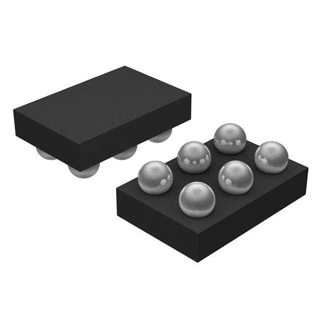
| 封装/外壳 | 10-WFDFN 裸露焊盘 |
| 工作温度 | -40°C ~ 125°C |
| 标准包装 | 121 |
| 电压-输入 | 4.3 V ~ 38 V |
| 电压-输出 | 5V |
| 电流-输出 | 1.2A |
| 类型 | 降压(降压) |
| 输出数 | 1 |
| 输出类型 | 固定 |
| 频率-开关 | 200kHz ~ 2MHz |


- 商务部:美国ITC正式对集成电路等产品启动337调查
- 曝三星4nm工艺存在良率问题 高通将骁龙8 Gen1或转产台积电
- 太阳诱电将投资9.5亿元在常州建新厂生产MLCC 预计2023年完工
- 英特尔发布欧洲新工厂建设计划 深化IDM 2.0 战略
- 台积电先进制程称霸业界 有大客户加持明年业绩稳了
- 达到5530亿美元!SIA预计今年全球半导体销售额将创下新高
- 英特尔拟将自动驾驶子公司Mobileye上市 估值或超500亿美元
- 三星加码芯片和SET,合并消费电子和移动部门,撤换高东真等 CEO
- 三星电子宣布重大人事变动 还合并消费电子和移动部门
- 海关总署:前11个月进口集成电路产品价值2.52万亿元 增长14.8%


PDF Datasheet 数据手册内容提取
LT3971/LT3971-3.3/LT3971-5 38V, 1.2A, 2MHz Step-Down Regulator with 2.8µA Quiescent Current FEATURES DESCRIPTION n Ultralow Quiescent Current: The LT®3971 is an adjustable frequency monolithic buck 2.8µA I Regulating 12V to 3.3V switching regulator that accepts a wide input voltage range Q IN OUT n Fixed Output Voltages: 3.3V, 5V, up to 38V. Low quiescent current design consumes only 2.1µA I Regulating 12V to 3.3V 2.8µA of supply current while regulating with no load. Low Q IN OUT n Low Ripple Burst Mode® Operation: ripple Burst Mode operation maintains high efficiency at Output Ripple < 15mV low output currents while keeping the output ripple below P-P n Wide Input Voltage Range: 4.3V to 38V 15mV in a typical application. An internally compensated n 1.2A Maximum Output Current current mode topology is used for fast transient response n Adjustable Switching Frequency: 200kHz to 2MHz and good loop stability. A high efficiency 0.33Ω switch n Synchronizable Between 250kHz to 2MHz is included on the die along with a boost Schottky diode n Fast Transient Response and the necessary oscillator, control and logic circuitry. n Accurate 1V Enable Pin Threshold An accurate 1V threshold enable pin can be used to shut n Low Shutdown Current: I = 700nA down the LT3971, reducing the input supply current to Q n Power Good Flag 700nA. A capacitor on the SS pin provides a controlled n Soft-Start Capability inrush current (soft-start). A power good flag signals n Internal Compensation when V reaches 91% of the programmed output volt- OUT n Output Voltage: 1.19V to 30V age. The LT3971 is available in small 10-lead MSOP and n Small Thermally Enhanced 10-Lead MSOP, 16-Lead 3mm × 3mm DFN packages with exposed pads for low MSOP and (3mm × 3mm) DFN Packages thermal resistance. A 16-lead MSOP is also offered which has enhanced pin-to-pin fault tolerance. APPLICATIONS L, LT, LTC, LTM, Linear Technology, the Linear logo and Burst Mode are registered trademarks of Linear Technology Corporation. All other trademarks are the property of their respective n Automotive Battery Regulation owners. n Power for Portable Products n Industrial Supplies TYPICAL APPLICATION No Load Supply Current 3.3V Step Down Converter 3.0 VIN OUTPUT IN REGULATION 4.5V TO 38V VIN OFF ON EN BOOST 2.5 LT3971-5 PG SW 0.47µF 4.7µH NT (µA) 4.7µF SS LT3971-3.3 RRE 2.0 U LT3971-3.3 RT C T BD PU VOUT IN 1.5 49.9k VOUT 3.3V SYNC GND 1.2A 22µF f = 800kHz 1.0 3971 TA01 5 10 15 20 25 30 35 INPUT VOLTAGE (V) 3971 TA01b 3971fd 1
LT3971/LT3971-3.3/LT3971-5 ABSOLUTE MAXIMUM RATINGS (Note 1) V , EN Voltage .........................................................38V Operating Junction Temperature Range (Note 2) IN BOOST Pin Voltage ...................................................55V LT3971E .............................................–40°C to 125°C BOOST Pin Above SW Pin .........................................30V LT3971I ..............................................–40°C to 125°C FB, V , RT, SYNC, SS Voltage .................................6V Storage Temperature Range ..............–65°C to 150°C OUT PG, BD Voltage .........................................................30V Lead Temperature (Soldering, 10 sec) Boost Diode Current ....................................................1A (MSE Only) .......................................................300°C PIN CONFIGURATION LT3971 LT3971 LT3971 TOP VIEW TOP VIEW TOP VIEW BD 1 16 GND BD 1 10 SYNC BD 1 10 SYNC NC 2 15 SYNC BOOST 2 9 PG BOOST 2 9 PG BOOST 3 14 PG 11 11 NC 4 17 13 RT SW 3 8 RT SW 3 8 RT GND GND SW 5 GND 12 SS VIN 4 7 SS VEINN 45 76 SFBS NC 6 11 NC EN 5 6 FB VIN 7 10 FB MSE PACKAGE EN 8 9 FB 10-LEAD PLASTIC MSOP MSE PACKAGE DD PACKAGE 10-LEAD (3mm × 3mm) PLASTIC DFN EXPOSED PAD (PINθ J1A1 =) 4IS5 °GCN, Dθ,J CM =U 1S0T° BCE/W S OLDERED TO PCB 16-LEAD PLASTIC MSOP EXPOSED PAD (PINθ J1A1 =) 4IS5 °GCN, Dθ,J CM =U 1S0T° BCE/W S OLDERED TO PCB EXPOSED PAD (PIN 17) ISθ GJAN =D ,4 M0°UCS T BE SOLDERED TO PCB LT3971-3.3, LT3971-5 LT3971-3.3, LT3971-5 TOP VIEW TOP VIEW BD 1 10 SYNC BD 1 10 SYNC BOOST 2 9 PG BOOST 2 9 PG 11 11 SW 3 8 RT SW 3 8 RT GND GND VIN 4 7 SS VEINN 45 76 SVOSUT EN 5 6 VOUT MSE PACKAGE 10-LEAD PLASTIC MSOP DD PACKAGE 10-LEAD (3mm × 3mm) PLASTIC DFN θJA = 45°C, θJC = 10°C/W EXPOSED PAD (PIN 11) IS GND, MUST BE SOLDERED TO PCB θJA = 45°C, θJC = 10°C/W EXPOSED PAD (PIN 11) IS GND, MUST BE SOLDERED TO PCB ORDER INFORMATION LEAD FREE FINISH TAPE AND REEL PART MARKING* PACKAGE DESCRIPTION TEMPERATURE RANGE LT3971EDD#PBF LT3971EDD#TRPBF LFJF 10-Lead (3mm × 3mm) Plastic DFN –40°C to 125°C LT3971IDD#PBF LT3971IDD#TRPBF LFJF 10-Lead (3mm × 3mm) Plastic DFN –40°C to 125°C LT3971EMSE#PBF LT3971EMSE#TRPBF LTFJG 10-Lead Plastic MSOP –40°C to 125°C LT3971IMSE#PBF LT3971IMSE#TRPBF LTFJG 10-Lead Plastic MSOP –40°C to 125°C LT3971EMSE16#PBF LT3971EMSE16#TRPBF 3971 16-Lead Plastic MSOP –40°C to 125°C LT3971IMSE16#PBF LT3971IMSE16#TRPBF 3971 16-Lead Plastic MSOP –40°C to 125°C LT3971EDD-3.3#PBF LT3971EDD-3.3#TRPBF LFRM 10-Lead (3mm × 3mm) Plastic DFN –40°C to 125°C LT3971IDD-3.3#PBF LT3971IDD-3.3#TRPBF LFRM 10-Lead (3mm × 3mm) Plastic DFN –40°C to 125°C LT3971EMSE-3.3#PBF LT3971EMSE-3.3#TRPBF LTFRN 10-Lead Plastic MSOP –40°C to 125°C LT3971IMSE-3.3#PBF LT3971IMSE-3.3#TRPBF LTFRN 10-Lead Plastic MSOP –40°C to 125°C 3971fd 2
LT3971/LT3971-3.3/LT3971-5 ORDER INFORMATION LEAD FREE FINISH TAPE AND REEL PART MARKING* PACKAGE DESCRIPTION TEMPERATURE RANGE LT3971EDD-5#PBF LT3971EDD-5#TRPBF LFRP 10-Lead (3mm × 3mm) Plastic DFN –40°C to 125°C LT3971IDD-5#PBF LT3971IDD-5#TRPBF LFRP 10-Lead (3mm × 3mm) Plastic DFN –40°C to 125°C LT3971EMSE-5#PBF LT3971EMSE-5#TRPBF LTFRQ 10-Lead Plastic MSOP –40°C to 125°C LT3971IMSE-5#PBF LT3971IMSE-5#TRPBF LTFRQ 10-Lead Plastic MSOP –40°C to 125°C Consult LTC Marketing for parts specified with wider operating temperature ranges. *The temperature grade is identified by a label on the shipping container. Consult LTC Marketing for information on non-standard lead based finish parts. For more information on lead free part marking, go to: http://www.linear.com/leadfree/ For more information on tape and reel specifications, go to: http://www.linear.com/tapeandreel/ ELECTRICAL CHARACTERISTICS The l denotes the specifications which apply over the full operating temperature range, otherwise specifications are at T = 25°C. V = 12V, V = 12V, V = 3.3V unless otherwise noted. (Note 2) A IN EN BD PARAMETER CONDITIONS MIN TYP MAX UNITS Minimum Input Voltage (Note 4) l 4 4.3 V Quiescent Current from V V Low 0.7 1.2 μA IN EN V High, V Low 1.7 2.7 μA EN SYNC V High, V Low l 4.5 μA EN SYNC LT3971 FB Pin Current V = 1.19V l 0.1 12 nA FB Internal Feedback Resistor Divider (LT3971-X) 10 MΩ Feedback Voltage 1.175 1.19 1.205 V l 1.165 1.19 1.215 V LT3971-3.3 Output Voltage 3.25 3.3 3.35 V l 3.224 3.3 3.376 V LT3971-5 Output Voltage 4.93 5 5.07 V l 4.89 5 5.11 V FB Voltage Line Regulation 4.3V < V < 38V (Note 4) 0.0002 0.01 %/V IN Switching Frequency R = 11k 1.6 2 2.4 MHz T R = 35.7k 0.8 1 1.2 MHz T R = 255k 160 200 240 kHz T Minimum Switch On Time 80 ns Minimum Switch Off Time 110 150 ns Switch Current Limit 1.8 2.4 3 A Switch V I = 1A 330 mV CESAT SW Switch Leakage Current 0.02 1 μA Boost Schottky Forward Voltage I = 100mA 770 mV SH Boost Schottky Reverse Leakage V = 12V 0.02 1 μA REVERSE Minimum Boost Voltage (Note 3) V = 5V l 1.4 1.8 V IN BOOST Pin Current I = 1A, V = 15V 20 28 mA SW BOOST EN Voltage Threshold EN Rising l 0.95 1.01 1.07 V EN Voltage Hysteresis 30 mV EN Pin Current 0.2 20 nA LT3971 PG Threshold Offset from V V Rising 60 100 140 mV FB FB LT3971 PG Hysteresis 20 mV LT3971-X PG Threshold Offset from V V Rising 5.5 9 12.5 % OUT OUT LT3971-X PG Hysteresis 1.3 % 3971fd 3
LT3971/LT3971-3.3/LT3971-5 ELECTRICAL CHARACTERISTICS The l denotes the specifications which apply over the full operating temperature range, otherwise specifications are at T = 25°C. V = 12V, V = 12V, V = 3.3V unless otherwise noted. (Note 2) A IN EN BD PG Leakage V = 3V 0.02 1 µA PG PG Sink Current V = 0.4V l 300 570 μA PG SYNC Threshold 0.6 0.8 1.0 V SYNC Pin Current 0.1 nA SS Source Current V = 1V 0.6 1 1.6 μA SS Note 1: Stresses beyond those listed under Absolute Maximum Ratings temperature range. High junction temperatures degrade operating may cause permanent damage to the device. Exposure to any Absolute lifetimes. Operating lifetime is derated at junction temperatures greater Maximum Rating condition for extended periods may affect device than 125°C. reliability and lifetime. Note 3: This is the minimum voltage across the boost capacitor needed to Note 2: The LT3971E is guaranteed to meet performance specifications guarantee full saturation of the switch. from 0°C to 125°C junction temperature. Specifications over the –40°C Note 4: This is the minimum input voltage for operation with accurate FB to 125°C operating junction temperature range are assured by design, regulation. Minimum input voltage for output regulation depends on the characterization, and correlation with statistical process controls. The application circuit. LT3971I is guaranteed over the full –40°C to 125°C operating junction TYPICAL PERFORMANCE CHARACTERISTICS T = 25°C, unless otherwise noted. A Efficiency, V = 5V Efficiency, V = 3.3V Efficiency, V = 5V OUT OUT OUT 100 100 100 VOUT = 5V 90 VIN = 12V 90 90 R1 = 1M VIN = 12V 80 R2 = 309k 80 80 70 VIN = 12V CY (%) 70 VIN = 24V VIN = 36V CY (%) 70 VIN = 36V VIN = 24V CY (%) 60 VIN = 24V VIN = 36V N 60 N 60 N 50 E E E CI CI CI EFFI 50 EFFI 50 EFFI 40 30 40 40 20 30 VRO1U =T 1=M 5V 30 10 R2 = 309k 20 20 0 0 0.2 0.4 0.6 0.8 1 1.2 0 0.2 0.4 0.6 0.8 1 1.2 0.01 0.1 1 10 100 1000 LOAD CURRENT (A) LOAD CURRENT (A) LOAD CURRENT (mA) 3971 G01 3971 G02 3971 G03 Efficiency, V = 3.3V No Load Supply Current No Load Supply Current OUT 90 100 4.0 DIODES, INC. 80 DFLS2100 VIN = 12V 3.5 70 NCY (%) 5600 VIN = 24V VIN = 36V RRENT (µA) 10 RRENT (µA) 32..05 LVTO3U9T7 =1 3.3V EFFICIE 3400 INPUT CU INPUT CU 2.0 LT3971-L5T3971-3.3 20 1.5 10 0 1 1.0 0.01 0.1 1 10 100 1000 –55 –25 5 35 65 95 125 155 5 10 15 20 25 30 35 LOAD CURRENT (mA) TEMPERATURE (°C) INPUT VOLTAGE (V) 3971 G04 3971 G05 3971 G06 3971fd 4
LT3971/LT3971-3.3/LT3971-5 TYPICAL PERFORMANCE CHARACTERISTICS T = 25°C, unless otherwise noted. A LT3971 Feedback Voltage LT3971-3.3 Output Voltage LT3971-5 Output Voltage 1.205 3.345 5.06 1.200 3.330 5.04 GE (V)1.195 E (V) 3.315 E (V) 5.02 A G G OLT LTA LTA V1.190 O 3.300 O 5.00 CK T V T V A U U B P P ED1.185 UT 3.285 UT 4.98 E O O F 1.180 3.270 4.96 1.175 3.255 4.94 –55 –25 5 35 65 95 125 155 –55 –25 5 35 65 95 125 155 –55 –25 5 35 65 95 125 155 TEMPERATURE (°C) TEMPERATURE (°C) TEMPERATURE (°C) 3971 G07 3971 G28 3971 G29 Maximum Load Current Maximum Load Current Load Regulation 3.0 2.5 0.30 VOUT = 3.3V VOUT = 5V 0.25 2.5 0.20 2.0 RRENT (A) 12..50 TYPICALMINIMUM RRENT (A) 1.5 TYPICALMINIMUM ULATION (%) 000...1105050 U U G OAD C 1.0 OAD C 1.0 AD RE––00..1005 L L O L–0.15 0.5 0.5 –0.20 –0.25 REFERENCED FROM VOUT AT 0.5A LOAD 0 0 –0.30 5 10 15 20 25 30 35 40 5 10 15 20 25 30 35 40 0 200 400 600 800 1000 1200 INPUT VOLTAGE (V) INPUT VOLTAGE (V) LOAD CURRENT (mA) 3971 G08 3971 G09 3971 G10 Switching Frequency Switch Current Limit Switch Current Limit 1000 3.0 2.5 2.4 950 2.5 Y (kHz) 980500 NT LIMIT (A) 2.0 NT LIMIT (A) 222...321 NC 800 RE 1.5 RE 2.0 FREQUE 775000 WITCH CUR 1.0 WITCH CUR 11..89 S S 1.7 0.5 650 1.6 DUTY CYCLE = 30% 600 0 1.5 –55 –25 5 35 65 95 125 155 0 20 40 60 80 100 –55 –25 5 35 65 95 125 155 TEMPERATURE (°C) DUTY CYCLE (%) TEMPERATURE (°C) 3971 G11 3971 G12 3971 G13 3971fd 5
LT3971/LT3971-3.3/LT3971-5 TYPICAL PERFORMANCE CHARACTERISTICS T = 25°C, unless otherwise noted. A Switch V Boost Pin Current Frequency Foldback CESAT 600 30 900 800 V (mV)CESAT435000000 PIN CURRENT (mA) 212055 NG FREQUENCY (kHz) 456700000000 200 OST 10 TCHI 300 BO WI 200 100 5 S 100 0 0 0 0 250 500 750 1000 1250 1500 0 250 500 750 1000 1250 1500 0 0.2 0.4 0.6 0.8 1 1.2 SWITCH CURRENT (mA) SWITCH CURRENT (mA) FB PIN VOLTAGE (V) 3971 G14 3971 G15 3971 G16 Minimum Switch On-Time/ LT3971-X Frequency Foldback Switch Off-Time Soft-Start 900 400 2.5 800 350 SWITCHING FREQUENCY (kHz) 765432000000000000 SWITCH ON/OFF TIME (ns) 122315050000000 MIN TOFF 0.5A LMOAIND TOFF 1AM LIONA TDON SWITCH CURRENT LIMIT (A) 2011....0505 100 50 0 0 0 0 20 40 60 80 100 –55 –25 5 35 65 95 125 155 0 0.25 0.5 0.75 1 1.25 1.5 1.75 2 VOUT (% OF REGULATION VOLTAGE) TEMPERATURE (°C) SS PIN VOLTAGE (V) 3971 G30 3971 G17 3971 G18 Minimum Input Voltage Minimum Input Voltage EN Threshold 5.0 6.4 1.05 VOUT = 3.3V VOUT = 5V 4.8 1.04 6.2 4.6 1.03 V) UT VOLTAGE (V) 4443....0248 TO START UT VOLTAGE (V) 565...608 TO START HOLD VOLTAGE ( 1110....00092109 RISING THRESHOLD INP 3.6 TO RUN INP 5.4 HRES 0.98 FALLING THRESHOLD T 3.4 0.97 5.2 TO RUN 3.2 0.96 3.0 5.0 0.95 0 200 400 600 800 1000 1200 0 200 400 600 800 1000 1200 –55 –25 5 35 65 95 125 155 LOAD CURRENT (mA) LOAD CURRENT (mA) TEMPERATURE (°C) 3971 G19 3971 G20 3971 G21 3971fd 6
LT3971/LT3971-3.3/LT3971-5 TYPICAL PERFORMANCE CHARACTERISTICS T = 25°C, unless otherwise noted. A Transient Load Response, Load Current Stepped from 25mA Boost Diode Forward Voltage Power Good Threshold (Burst Mode Operation) to 525mA 1.6 95 1.4 94 1.2 %) 93 VOUT E VF (V) 1.0 LTAGE ( 9921 100mV/DIV D O DIO 0.8 D V 90 BOOST 0.6 RESHOL 8889 0.4 H T 87 0.2 IL 86 500mA/DIV 0 85 0 250 500 750 1000 1250 1500 –55 –25 5 35 65 95 125 155 10µs/DIV 3971 G24 BOOST DIODE CURRENT (mA) TEMPERATURE (°C) VIN = 12V, VOUT = 3.3V 3971 G22 3971 G23 COUT = 47µF Transient Load Response, Load Current Stepped from Switching Waveforms; Switching Waveforms; Full 0.5A to 1A Burst Mode Operation Frequency Continuous Operation 100VmOUVT/ VSW 5VV/DSIWV DIV 5V/DIV IL IL 500mA/DIV 500mA/DIV IL 500mA/ DIV VOUT VOUT 20mV/DIV 20mV/DIV 10µs/DIV 3971 G25 5µs/DIV 3971 G26 1µs/DIV 3971 G27 VIN = 12V, VOUT = 3.3V VIN = 12V, VOUT = 3.3V VIN = 12V, VOUT = 3.3V COUT = 47µF ILOAD = 10mA ILOAD = 1A COUT = 22µF COUT = 22µF 3.3V Start-Up and Dropout 3.3V Start-Up and Dropout 5V Start-Up and Dropout VIN VIN VIN V V V DI DI DI V/ V/ V/ 1 1 1 VOUT VOUT VOUT 0.5s/DIV 3971 G31 0.5s/DIV 3971 G32 0.5s/DIV 3971 G33 800kHz 800kHz 800kHz 3kΩ LOAD 6.7Ω LOAD 5kΩ LOAD 3971fd 7
LT3971/LT3971-3.3/LT3971-5 TYPICAL PERFORMANCE CHARACTERISTICS T = 25°C, unless otherwise noted. A 5V Start-Up and Dropout Feedback Regulation Voltage Minimum Input Voltage to Switch 1.6 5 VIN V) 1.2 4 1V/DIV VOUT FEEDBACK VOLTAGE ( 00..48 INPUT VOLTAGE (V) 23 0 1 0.5s/DIV 3971 G34 2 2.5 3 3.5 4 4.5 5 –55 –25 5 35 65 95 125 155 800kHz INPUT VOLTAGE (V) TEMPERATURE (°C) 10Ω LOAD 3971 G35 3971 G36 PIN FUNCTIONS (DFN, MSE10/MSE16) BD (Pin 1/Pin 1): This pin connects to the anode of the SS (Pin 7/Pin 12): A capacitor is tied between SS and boost diode. The BD pin is normally connected to the output. ground to slowly ramp up the peak current limit of the LT3971 on start-up. The soft-start capacitor is only actively BOOST (Pin 2/Pin 3): This pin is used to provide a drive discharged when EN is low. The SS pin is released when voltage, higher than the input voltage, to the internal bipolar the EN pin goes high. Float this pin to disable soft-start. NPN power switch. For applications with input voltages above 25V, add a 100k SW (Pin 3/Pin 5): The SW pin is the output of an internal resistor in series with the soft-start capacitor. power switch. Connect this pin to the inductor, catch diode, RT (Pin 8/Pin 13): A resistor is tied between RT and ground and boost capacitor. to set the switching frequency. V (Pin 4/Pin 7): The V pin supplies current to the IN IN PG (Pin 9/Pin 14): The PG pin is the open-drain output of LT3971’s internal circuitry and to the internal power switch. an internal comparator. PGOOD remains low until the FB This pin must be locally bypassed. pin is within 9% of the final regulation voltage. PGOOD is EN (Pin 5/Pin 8): The part is in shutdown when this pin valid when the LT3971 is enabled and V is above 4.3V. IN is low and active when this pin is high. The hysteretic SYNC (Pin 10/Pin 15): This is the external clock synchro- threshold voltage is 1.005V going up and 0.975V going nization input. Ground this pin for low ripple Burst Mode down. The EN threshold is only accurate when V is above IN operation at low output loads. Tie to a clock source for 4.3V. If V is lower than 4.2V, ground EN to place the part IN synchronization, which will include pulse-skipping at low in shutdown. Tie to V if shutdown feature is not used. IN output loads. When in pulse-skipping mode, quiescent FB (Pin 6, LT3971 Only/Pins 9, 10): The LT3971 regulates current increases to 1.5mA. the FB pin to 1.19V. Connect the feedback resistor divider GND (Exposed Pad Pin 11/Pin 16, Exposed Pad Pin 17): tap to this pin. Also, connect a phase lead capacitor between Ground. The exposed pad must be soldered to PCB. FB and V . Typically this capacitor is 10pF. OUT NC (None/Pins 2, 4, 6, 11): No Connect. These pins V (Pin 6, LT3971-3.3 and LT3971-5 Only): The OUT are not connected to internal circuitry. Float these pins LT3971-3.3 and LT3971-5 regulate the V pin to 3.3V and OUT to achieve FMEA fault tolerance. (See Fault Tolerance of 5V respectively. This pin connects to the internal 10MΩ MS16E Package section.) feedback divider that programs the fixed output voltage. 3971fd 8
LT3971/LT3971-3.3/LT3971-5 BLOCK DIAGRAM VIN C1 VIN – INTERNAL 1.19V REF + BD 1V + SWITCH – SHDN Σ SLOPE COMP LATCH BOOST EN R OSCILLATOR Q C3 RT 200kHz TO 2MHz S RT L1 VOUT SW Burst Mode SYNC DETECT D1 C2 PG ERROR AMP VC CLAMP + 1.09V + VC 1µA – – C5 SS SHDN R3 R2 R1 C4 GND FB VOUT LT3971-3.3 LT3971-5 R2 R1 ONLY 3991 BD LT3971 LT3971-3.3: R1 = 6.39M, R2 = 3.61M ONLY C5 LT3971-5: R1 = 7.62M, R2 = 2.38M 3971fd 9
LT3971/LT3971-3.3/LT3971-5 OPERATION The LT3971 is a constant frequency, current mode step- voltage at the BOOST pin that is higher than the input down regulator. An oscillator, with frequency set by RT, supply. This allows the driver to fully saturate the internal sets an RS flip-flop, turning on the internal power switch. bipolar NPN power switch for efficient operation. An amplifier and comparator monitor the current flowing To further optimize efficiency, the LT3971 automatically between the V and SW pins, turning the switch off when IN switches to Burst Mode operation in light load situations. this current reaches a level determined by the voltage at Between bursts, all circuitry associated with controlling V (see Block Diagram). An error amplifier measures the C the output switch is shut down, reducing the input supply output voltage through an external resistor divider tied to current to 1.7μA. In a typical application, 2.8μA will be the FB pin and servos the V node. If the error amplifier’s C consumed from the supply when regulating with no load. output increases, more current is delivered to the output; if it decreases, less current is delivered. An active clamp The oscillator reduces the LT3971’s operating frequency on the V node provides current limit. The V node is when the voltage at the FB pin is low. This frequency C C also clamped by the voltage on the SS pin; soft-start is foldback helps to control the output current during start- implemented by generating a voltage ramp at the SS pin up and overload. using an external capacitor. The LT3971 contains a power good comparator which If the EN pin is low, the LT3971 is shut down and draws trips when the FB pin is at 91% of its regulated value. The 700nA from the input. When the EN pin exceeds 1V, the PG output is an open-drain transistor that is off when the switching regulator will become active. output is in regulation, allowing an external resistor to pull the PG pin high. Power good is valid when the LT3971 is The switch driver operates from either V or from the IN enabled and V is above 4.3V. IN BOOST pin. An external capacitor is used to generate a APPLICATIONS INFORMATION Achieving Ultralow Quiescent Current 1000 VIN = 12V VOUT = 3.3V To enhance efficiency at light loads, the LT3971 operates in low ripple Burst Mode, which keeps the output capacitor kHz)800 Y ( charged to the desired output voltage while minimizing NC E600 U the input quiescent current. In Burst Mode operation the Q E R LT3971 delivers single pulses of current to the output ca- G F400 N pacitor followed by sleep periods where the output power HI C T is supplied by the output capacitor. When in sleep mode SWI200 the LT3971 consumes 1.7μA, but when it turns on all the circuitry to deliver a current pulse, the LT3971 consumes 0 0 20 40 60 80 100 120 1.5mA of input current in addition to the switch current. LOAD CURRENT (mA) Therefore, the total quiescent current will be greater than 3971 F01 Figure 1. Switching Frequency in Burst Mode Operation 1.7μA when regulating. gets closer to the 1.7μA ideal. Therefore, to optimize the As the output load decreases, the frequency of single cur- quiescent current performance at light loads, the current rent pulses decreases (see Figure 1) and the percentage in the feedback resistor divider and the reverse current of time the LT3971 is in sleep mode increases, resulting in the catch diode must be minimized, as these appear in much higher light load efficiency. By maximizing the to the output as load currents. Use the largest possible time between pulses, the converter quiescent current 3971fd 10
LT3971/LT3971-3.3/LT3971-5 APPLICATIONS INFORMATION feedback resistors and a low leakage Schottky catch diode programmed by the R resistor, and will be operating in T in applications utilizing the ultralow quiescent current standard PWM mode. The transition between PWM and low performance of the LT3971. The feedback resistors should ripple Burst Mode operation will exhibit slight frequency preferably be on the order of MΩ and the Schottky catch jitter, but will not disturb the output voltage. diode should have less than 1µA of typical reverse leak- To ensure proper Burst Mode operation, the SYNC pin age at room temperature. These two considerations are must be grounded. When synchronized with an external reiterated in the FB Resistor Network and Catch Diode clock, the LT3971 will pulse skip at light loads. The qui- Selection sections. escent current will significantly increase to 1.5mA in light It is important to note that another way to decrease the load situations when synchronized with an external clock. pulse frequency is to increase the magnitude of each Holding the SYNC pin high yields no advantages in terms single current pulse. However, this increases the output of output ripple or minimum load to full frequency, so is voltage ripple because each cycle delivers more power to not recommended. the output capacitor. The magnitude of the current pulses FB Resistor Network was selected to ensure less than 15mV of output ripple in a typical application. See Figure 2. The output voltage is programmed with a resistor divider between the output and the FB pin. Choose the resistor values according to: VSW 5V/DIV V R1=R2 OUT −1 1.19V IL 500mA/DIV Reference designators refer to the Block Diagram. 1% resistors are recommended to maintain output voltage VOUT 20mV/DIV accuracy. 5µs/DIV 3971 F02 The total resistance of the FB resistor divider should be VIN = 12V VOUT = 3.3V selected to be as large as possible to enhance low current ILOAD = 10mA performance. The resistor divider generates a small load Figure 2. Burst Mode Operation on the output, which should be minimized to optimize the low supply current at light loads. While in Burst Mode operation, the burst frequency and When using large FB resistors, a 10pF phase lead capacitor the charge delivered with each pulse will not change with should be connected from V to FB. output capacitance. Therefore, the output voltage ripple OUT will be inversely proportional to the output capacitance. The LT3971-3.3 and LT3971-5 contain an internal 10M FB In a typical application with a 22μF output capacitor, the resistor divider as well as an internal phase lead capacitor. output ripple is about 10mV, and with a 47μF output ca- pacitor the output ripple is about 5mV. The output voltage Setting the Switching Frequency ripple can continue to be decreased by increasing the The LT3971 uses a constant frequency PWM architecture output capacitance. that can be programmed to switch from 200kHz to 2MHz At higher output loads (above 92mA for the front page by using a resistor tied from the RT pin to ground. A table application) the LT3971 will be running at the frequency showing the necessary RT value for a desired switching frequency is in Table 1. 3971fd 11
LT3971/LT3971-3.3/LT3971-5 APPLICATIONS INFORMATION switch off-time. These equations show that duty cycle Table 1. Switching Frequency vs R Value T range increases when switching frequency is decreased. SWITCHING FREQUENCY (MHz) R VALUE (kΩ) T 0.2 255 A good choice of switching frequency should allow 0.4 118 adequate input voltage range (see Input Voltage Range 0.6 71.5 0.8 49.9 section) and keep the inductor and capacitor values small. 1.0 35.7 1.2 28.0 Input Voltage Range 1.4 22.1 1.6 17.4 The minimum input voltage is determined by either the 1.8 14.0 2.0 11.0 LT3971’s minimum operating voltage of 4.3V or by its maximum duty cycle (see equation in Operating Frequency Operating Frequency Tradeoffs Tradeoffs section). The minimum input voltage due to duty cycle is: Selection of the operating frequency is a tradeoff between efficiency, component size, minimum dropout voltage, and V +V maximum input voltage. The advantage of high frequency VIN(MIN)= OUT D −VD+VSW 1−f t operation is that smaller inductor and capacitor values may SW OFF(MIN) be used. The disadvantages are lower efficiency, lower where V is the minimum input voltage, V is IN(MIN) OUT maximum input voltage, and higher dropout voltage. The the output voltage, V is the catch diode drop (~0.5V), D highest acceptable switching frequency (f ) for a SW(MAX) V is the internal switch drop (~0.5V at max load), f SW SW given application can be calculated as follows: is the switching frequency (set by R ), and t is T OFF(MIN) V +V the minimum switch off-time. Note that higher switch- f = OUT D SW(MAX) ing frequency will increase the minimum input voltage. t (V −V +V ) ON(MIN) IN SW D If a lower dropout voltage is desired, a lower switching frequency should be used. where V is the typical input voltage, V is the output IN OUT voltage, VD is the catch diode drop (~0.5V), and VSW is The maximum input voltage for LT3971 applications the internal switch drop (~0.5V at max load). This equation depends on switching frequency, the Absolute Maximum shows that slower switching frequency is necessary to Ratings of the V and BOOST pins, and the operating IN safely accommodate high VIN/VOUT ratio. Also, as shown mode. For a given application where the switching fre- in the Input Voltage Range section, lower frequency allows quency and the output voltage are already selected, the a lower dropout voltage. The input voltage range depends maximum input voltage (V ) that guarantees IN(OP-MAX) on the switching frequency because the LT3971 switch has optimum output voltage ripple for that application can be finite minimum on and off times. The minimum switch on found by applying the following equation: and off times are strong functions of temperature. Use V +V the typical minimum on and off curves to design for an V = OUT D –V +V IN(OP-MAX) D SW application’s maximum temperature, while adding about f •t SW ON(MIN) 30% for part-to-part variation. The minimum and maximum duty cycles that can be achieved taking minimum on and where tON(MIN) is the minimum switch on-time. Note that off times into account are: a higher switching frequency will decrease the maximum operating input voltage. Conversely, a lower switching DC =f t MIN SW ON(MIN) frequency will be necessary to achieve normal operation DC =1−f t at higher input voltages. MAX SW OFF(MIN) The circuit will tolerate inputs above the maximum op- where f is the switching frequency, the t is the SW ON(MIN) erating input voltage and up to the Absolute Maximum minimum switch on-time, and the t is the minimum OFF(MIN) 3971fd 12
LT3971/LT3971-3.3/LT3971-5 APPLICATIONS INFORMATION Ratings of the V and BOOST pins, regardless of chosen Table 2. Inductor Vendors IN switching frequency. However, during such transients VENDOR URL PART SERIES TYPE where VIN is higher than VIN(OP-MAX), the LT3971 will enter Murata www.murata.com LQH55D Open pulse-skipping operation where some switching pulses are TDK www.componenttdk.com SLF7045 Shielded skipped to maintain output regulation. The output voltage SLF10145 Shielded ripple and inductor current ripple will be higher than in Toko www.toko.com D62CB Shielded D63CB Shielded typical operation. Do not overload when V is greater IN D73C Shielded than VIN(OP-MAX). D75F Open Coilcraft www.coilcraft.com MSS7341 Shielded Inductor Selection and Maximum Output Current MSS1038 Shielded Sumida www.sumida.com CR54 Open A good first choice for the inductor value is: CDRH74 Shielded CDRH6D38 Shielded V +V L= OUT D CR75 Open f SW When the switch is off, the potential across the inductor where f is the switching frequency in MHz, V is the is the output voltage plus the catch diode drop. This gives SW OUT output voltage, V is the catch diode drop (~0.5V) and L the peak-to-peak ripple current in the inductor: D is the inductor value in μH. (1−DC)•(V +V ) ΔI = OUT D The inductor’s RMS current rating must be greater than the L L•f SW maximum load current and its saturation current should be about 30% higher. For robust operation in fault conditions Where f is the switching frequency of the LT3971, DC is SW (start-up or short-circuit) and high input voltage (>30V), the duty cycle and L is the value of the inductor. Therefore, the saturation current should be above 3.8A. To keep the the maximum output current that the LT3971 will deliver efficiency high, the series resistance (DCR) should be less depends on the switch current limit, the inductor value, than 0.1Ω, and the core material should be intended for and the input and output voltages. The inductor value may high frequency applications. Table 2 lists several vendors have to be increased if the inductor ripple current does and suitable types. not allow sufficient maximum output current (I ) OUT(MAX) given the switching frequency, and maximum input voltage The inductor value must be sufficient to supply the desired used in the desired application. maximum output current (I ), which is a function OUT(MAX) of the switch current limit (I ) and the ripple current. The optimum inductor for a given application may differ LIM from the one indicated by this simple design guide. A larger ΔI I =I – L value inductor provides a higher maximum load current OUT(MAX) LIM 2 and reduces the output voltage ripple. If your load is lower The LT3971 limits its peak switch current in order to than the maximum load current, than you can relax the protect itself and the system from overload faults. The value of the inductor and operate with higher ripple cur- LT3971’s switch current limit (I ) is at least 2.4A at low rent. This allows you to use a physically smaller inductor, LIM duty cycles and decreases linearly to 1.75A at DC = 0.8. or one with a lower DCR resulting in higher efficiency. Be aware that if the inductance differs from the simple rule above, then the maximum load current will depend on the input voltage. In addition, low inductance may result in discontinuous mode operation, which further reduces 3971fd 13
LT3971/LT3971-3.3/LT3971-5 APPLICATIONS INFORMATION maximum load current. For details of maximum output cur- Output Capacitor and Output Ripple rent and discontinuous operation, see Linear Technology’s The output capacitor has two essential functions. Along Application Note 44. Finally, for duty cycles greater than with the inductor, it filters the square wave generated by the 50% (V /V >0.5), a minimum inductance is required to OUT IN LT3971 to produce the DC output. In this role it determines avoid sub-harmonic oscillations. See Application Note 19. the output ripple, so low impedance (at the switching One approach to choosing the inductor is to start with frequency) is important. The second function is to store energy in order to satisfy transient loads and stabilize the the simple rule given above, look at the available induc- LT3971’s control loop. Ceramic capacitors have very low tors, and choose one to meet cost or space goals. Then equivalent series resistance (ESR) and provide the best use the equations above to check that the LT3971 will be ripple performance. A good starting value is: able to deliver the required output current. Note again that these equations assume that the inductor current is 100 C = continuous. Discontinuous operation occurs when I OUT OUT V f OUT SW is less than ΔI /2. L where f is in MHz, and C is the recommended output SW OUT Input Capacitor capacitance in μF. Use X5R or X7R types. This choice will provide low output ripple and good transient response. Bypass the input of the LT3971 circuit with a ceramic Transient performance can be improved with a higher capacitor of X7R or X5R type. Y5V types have poor value capacitor. Increasing the output capacitance will performance over temperature and applied voltage, and also decrease the output voltage ripple. A lower value of should not be used. A 4.7μF to 10μF ceramic capacitor output capacitor can be used to save space and cost but is adequate to bypass the LT3971 and will easily handle transient performance will suffer. the ripple current. Note that larger input capacitance is required when a lower switching frequency is used (due When choosing a capacitor, look carefully through the to longer on-times). If the input power source has high data sheet to find out what the actual capacitance is under impedance, or there is significant inductance due to operating conditions (applied voltage and temperature). A physically larger capacitor or one with a higher voltage rating long wires or cables, additional bulk capacitance may be may be required. Table 3 lists several capacitor vendors. necessary. This can be provided with a low performance electrolytic capacitor. Table 3. Recommended Ceramic Capacitor Vendors Step-down regulators draw current from the input sup- MANUFACTURER WEBSITE ply in pulses with very fast rise and fall times. The input AVX www.avxcorp.com capacitor is required to reduce the resulting voltage Murata www.murata.com ripple at the LT3971 and to force this very high frequency Taiyo Yuden www.t-yuden.com switching current into a tight local loop, minimizing EMI. Vishay Siliconix www.vishay.com A 4.7μF capacitor is capable of this task, but only if it is TDK www.tdk.com placed close to the LT3971 (see the PCB Layout section). A second precaution regarding the ceramic input capacitor Catch Diode Selection concerns the maximum input voltage rating of the LT3971. The catch diode (D1 from Block Diagram) conducts cur- A ceramic input capacitor combined with trace or cable rent only during switch off time. Average forward current inductance forms a high quality (under damped) tank in normal operation can be calculated from: circuit. If the LT3971 circuit is plugged into a live supply, the input voltage can ring to twice its nominal value, pos- V –V I =I IN OUT sibly exceeding the LT3971’s voltage rating. This situation D(AVG) OUT V IN is easily avoided (see the Hot Plugging Safely section). where I is the output load current. The only reason to OUT consider a diode with a larger current rating than necessary 3971fd 14
LT3971/LT3971-3.3/LT3971-5 APPLICATIONS INFORMATION for nominal operation is for the worst-case condition of An additional consideration is reverse leakage current. shorted output. The diode current will then increase to the When the catch diode is reversed biased, any leakage typical peak switch current. Peak reverse voltage is equal current will appear as load current. When operating under to the regulator input voltage. Use a diode with a reverse light load conditions, the low supply current consumed voltage rating greater than the input voltage. by the LT3971 will be optimized by using a catch diode with minimum reverse leakage current. Low leakage Table 4. Schottky Diodes. The Reverse Current Values Listed Are Schottky diodes often have larger forward voltage drops Estimates Based Off of Typical Curves for Reverse Current vs Reverse Voltage at 25°C. at a given current, so a trade-off can exist between low load and high load efficiency. Often Schottky diodes with I at V = R R VR IAVE VF at 1A VF at 2A 20V 25°C larger reverse bias ratings will have less leakage at a given PART NUMBER (V) (A) (mV) (mV) (µA) output voltage than a diode with a smaller reverse bias On Semiconductor rating. Therefore, superior leakage performance can be MBR0520L 20 0.5 30 achieved at the expense of diode size. Table 4 lists several MBR0540 40 0.5 620 0.4 Schottky diodes and their manufacturers. MBRM120E 20 1 530 595 0.5 MBRM140 40 1 550 20 Ceramic Capacitors Diodes Inc. Ceramic capacitors are small, robust and have very low B0530W 30 0.5 15 ESR. However, ceramic capacitors can cause problems B0540W 40 0.5 620 1 when used with the LT3971 due to their piezoelectric nature. B120 20 1 500 1.1 When in Burst Mode operation, the LT3971’s switching B130 30 1 500 1.1 frequency depends on the load current, and at very light B140 40 1 500 1.1 loads the LT3971 can excite the ceramic capacitor at audio B150 50 1 700 0.4 frequencies, generating audible noise. Since the LT3971 B220 20 2 500 20 operates at a lower current limit during Burst Mode op- B230 30 2 500 0.6 eration, the noise is typically very quiet to a casual ear. If B140HB 40 1 1 this is unacceptable, use a high performance tantalum or DFLS240L 40 2 500 4 electrolytic capacitor at the output. DFLS140 40 1.1 510 1 A final precaution regarding ceramic capacitors concerns DFLS160 60 1 500 2.5 the maximum input voltage rating of the LT3971. As pre- DFLS2100 100 2 770 860 0.01 viously mentioned, a ceramic input capacitor combined B240 40 2 500 0.45 with trace or cable inductance forms a high quality (under Central Semiconductor damped) tank circuit. If the LT3971 circuit is plugged into a CMSH1 - 40M 40 1 500 live supply, the input voltage can ring to twice its nominal CMSH1 - 60M 60 1 700 value, possibly exceeding the LT3971’s rating. This situation CMSH1 - 40ML 40 1 400 is easily avoided (see the Hot Plugging Safely section). CMSH2 - 40M 40 2 550 CMSH2 - 60M 60 2 700 BOOST and BD Pin Considerations CMSH2 - 40L 40 2 400 Capacitor C3 and the internal boost Schottky diode (see CMSH2 - 40 40 2 500 the Block Diagram) are used to generate a boost volt- CMSH2 - 60M 60 2 700 age that is higher than the input voltage. In most cases a 0.47μF capacitor will work well. Figure 3 shows three ways to arrange the boost circuit. The BOOST pin must be more than 2.3V above the SW pin for best efficiency. 3971fd 15
LT3971/LT3971-3.3/LT3971-5 APPLICATIONS INFORMATION For outputs of 3V and above, the standard circuit (Figure 3a) The minimum operating voltage of an LT3971 application is best. For outputs between 2.8V and 3V, use a 1μF boost is limited by the minimum input voltage (4.3V) and by capacitor. A 2.5V output presents a special case because it the maximum duty cycle as outlined in the Input Voltage is marginally adequate to support the boosted drive stage Range section. For proper start-up, the minimum input while using the internal boost diode. For reliable BOOST pin voltage is also limited by the boost circuit. If the input operation with 2.5V outputs use a good external Schottky voltage is ramped slowly, the boost capacitor may not diode (such as the ON Semi MBR0540), and a 1μF boost be fully charged. Because the boost capacitor is charged capacitor (Figure 3b). For output voltages below 2.5V, with the energy stored in the inductor, the circuit will rely the boost diode can be tied to the input (Figure 3c), or to on some minimum load current to get the boost circuit another external supply greater than 2.8V. However, the running properly. This minimum load will depend on input circuit in Figure 3a is more efficient because the BOOST pin and output voltages, and on the arrangement of the boost current comes from a lower voltage source. You must also circuit. The minimum load generally goes to zero once the be sure that the maximum voltage ratings of the BOOST circuit has started. Figure 4 shows a plot of minimum load and BD pins are not exceeded. to start and to run as a function of input voltage. In many cases the discharged output capacitor will present a load to the switcher, which will allow it to start. The plots show BD VIN VIN BOOST the worst-case situation where VIN is ramping very slowly. LT3971 C3 4.7µF SW VOUT 5.0 GND 4.8 4.6 V) 4.4 (3a) For VOUT > 2.8V AGE ( 4.2 TO START OLT 4.0 V T 3.8 TO RUN U P BD D2 IN 3.6 VIN VIN BOOST 3.4 VOUT = 3.3V TA = 25°C LT3971 C3 3.2 L = 4.7µH f = 800kHz 3.0 4.7µF GND SW VOUT 10 100 1000 LOAD CURRENT (mA) 6.4 6.2 (3b) For 2.5V < VOUT < 2.8V 6.0 TO START V) E ( AG 5.8 BD LT O VIN VIN BOOST T V 5.6 U TO RUN LT3971 C3 NP I 5.4 VOUT = 5V 4.7µF GND SW VOUT 5.2 TA = 25°C L = 4.7µH f = 800kHz 5.0 10 100 1000 3971 FO3 LOAD CURRENT (mA) 3971 F04 (3c) For VOUT < 2.5V; VIN(MAX) = 27V Figure 4. The Minimum Input Voltage Depends on Figure 3. Three Circuits for Generating the Boost Voltage Output Voltage, Load Current and Boost Circuit 3971fd 16
LT3971/LT3971-3.3/LT3971-5 APPLICATIONS INFORMATION For lower start-up voltage, the boost diode can be tied to Be aware that when the input voltage is below 4.3V, the V ; however, this restricts the input range to one-half of input current may rise to several hundred μA. And the part IN the absolute maximum rating of the BOOST pin. may be able to switch at cold or for V ) thresholds less IN(EN than 7V. Figure 6 shows the magnitude of the increased At light loads, the inductor current becomes discontinu- input current in a typical application with different pro- ous and this reduces the minimum input voltage to ap- grammed V . proximately 400mV above V . At higher load currents, IN(EN) OUT the inductor current is continuous and the duty cycle is When operating in Burst Mode for light load currents, the limited by the maximum duty cycle of the LT3971, requiring current through the V resistor network can easily be IN(EN) a higher input voltage to maintain regulation. greater than the supply current consumed by the LT3971. Therefore, the V resistors should be large to minimize IN(EN) Enable Pin their effect on efficiency at low loads. The LT3971 is in shutdown when the EN pin is low and 12V V Input Current active when the pin is high. The rising threshold of the IN(EN) 500 EN comparator is 1.01V, with 30mV of hysteresis. The EN pin can be tied to V if the shutdown feature is not used. IN 400 A) Adding a resistor divider from V to EN programs the µ IN T ( LT3971 to regulate the output only when VIN is above a REN 300 R desired voltage (see Figure 5). Typically, this threshold, U C T 200 V , is used in situations where the input supply is cur- U IN(EN) P N rent limited, or has a relatively high source resistance. A I 100 switching regulator draws constant power from the source, so source current increases as source voltage drops. This 0 looks like a negative resistance load to the source and can 0 1 2 3 4 5 6 7 8 9 10 11 12 INPUT VOLTAGE (V) cause the source to current limit or latch low under low VIN(EN) = 12V source voltage conditions. The V threshold prevents R3 = 11M IN(EN) R4 = 1M the regulator from operating at source voltages where the problems might occur. This threshold can be adjusted by 6V V Input Current IN(EN) setting the values R3 and R4 such that they satisfy the 500 following equation: 400 R3 A) VIN(EN)=R4+1 NT (µ 300 E R R U where output regulation should not start until V is above C IN T 200 U VIN(EN). Due to the comparator’s hysteresis, switching will INP not stop until the input falls slightly below V . IN(EN) 100 0 LT3971 VIN 0 1 2 3 4 5 6 INPUT VOLTAGE (V) R3 1V + VIN(EN) = 6V 3971 F06 EN SHDN R3 = 5M – R4 = 1M R4 Figure 6. Input Current vs Input Voltage 3971 F05 for a Programmed V of 6V and 12V IN(EN) Figure 5. Programmed Enable Threshold 3971fd 17
LT3971/LT3971-3.3/LT3971-5 APPLICATIONS INFORMATION Soft-Start The LT3971 will not enter Burst Mode operation at low output loads while synchronized to an external clock, but The SS pin can be used to soft-start the LT3971 by throttling instead will pulse skip to maintain regulation. the maximum input current during start-up. An internal 1μA current source charges an external capacitor generating a The LT3971 may be synchronized over a 250kHz to 2MHz voltage ramp on the SS pin. The SS pin clamps the internal range. The R resistor should be chosen to set the LT3971 T V node, which slowly ramps up the current limit. Maximum switching frequency 20% below the lowest synchronization C current limit is reached when the SS pin is about 1.5V or input. For example, if the synchronization signal will be higher. By selecting a large enough capacitor, the output 250kHz and higher, the R should be selected for 200kHz. T can reach regulation without overshoot. For applications To assure reliable and safe operation the LT3971 will only with input voltages above 25V, a 100k resistor in series synchronize when the output voltage is near regulation as with the soft-start capacitor is recommended. Figure 7 indicated by the PG flag. It is therefore necessary to choose shows start-up waveforms for a typical application with a large enough inductor value to supply the required output a 10nF capacitor on SS for a 3.3Ω load when the EN pin current at the frequency set by the R resistor (see the T is pulsed high for 13ms. Inductor Selection section). The slope compensation is set by the R value, while the minimum slope compensation The external SS capacitor is only actively discharged when T required to avoid subharmonic oscillations is established EN is low. With EN low, the external SS cap is discharged by the inductor size, input voltage, and output voltage. through approximately 150Ω. The EN pin needs to be low Since the synchronization frequency will not change the long enough for the external cap to completely discharge slopes of the inductor current waveform, if the inductor through the 150Ω pull-down prior to start-up. is large enough to avoid subharmonic oscillations at the frequency set by R , than the slope compensation will be T sufficient for all synchronization frequencies. VSS 1V/DIV Shorted and Reversed Input Protection VOUT If the inductor is chosen so that it won’t saturate exces- 2V/DIV sively, a LT3971 buck regulator will tolerate a shorted output. There is another situation to consider in systems IL 0.5A/DIV where the output will be held high when the input to the 2ms/DIV 3971 F07 LT3971 is absent. This may occur in battery charging ap- plications or in battery backup systems where a battery Figure 7. Soft-Start Waveforms for Front-Page Application with 10nF Capacitor on SS. EN is Pulsed High for About or some other supply is diode ORed with the LT3971’s 13ms with a 3.3Ω Load Resistor output. If the V pin is allowed to float and the EN pin IN is held high (either by a logic signal or because it is tied Synchronization to V ), then the LT3971’s internal circuitry will pull its IN To select low ripple Burst Mode operation, tie the SYNC quiescent current through its SW pin. This is fine if your pin below 0.6V (this can be ground or a logic low output). system can tolerate a few μA in this state. If you ground the EN pin, the SW pin current will drop to essentially Synchronizing the LT3971 oscillator to an external fre- zero. However, if the V pin is grounded while the output quency can be done by connecting a square wave (with IN is held high, regardless of EN, parasitic diodes inside the 20% to 80% duty cycle) to the SYNC pin. The square LT3971 can pull current from the output through the SW wave amplitude should have valleys that are below 0.6V pin and the V pin. Figure 8 shows a circuit that will run and peaks above 1.0V (up to 6V). IN only when the input voltage is present and that protects against a shorted or reversed input. 3971fd 18
LT3971/LT3971-3.3/LT3971-5 APPLICATIONS INFORMATION D4 MBRS140 VIN VIN BOOST L1 C2 VOUT EN SW VOUT LT3971 BD GND FB + BACKUP RPG GND C3 RT C4 3971 F07 Figure 8. Diode D4 Prevents a Shorted Input from Discharging a R2 Backup Battery Tied to the Output. It Also Protects the Circuit from C5 R1 a Reversed Input. The LT3971 Runs Only When the Input is Present PCB Layout D1 C1 For proper operation and minimum EMI, care must be taken GND during printed circuit board layout. Figure 9 shows the 3971 F09 recommended component placement with trace, ground VIAS TO LOCAL GROUND PLANE VIAS TO RUN/SS VIAS TO VIN plane and via locations. Note that large, switched currents VIAS TO VOUT VIAS TO SYNC VIAS TO PG OUTLINE OF LOCAL GROUND PLANE flow in the LT3971’s V and SW pins, the catch diode IN (D1), and the input capacitor (C1). The loop formed by Figure 9. A Good PCB Layout Ensures Proper, Low EMI Operation these components should be as small as possible. These components, along with the inductor and output capacitor, the V pin of the LT3971 can ring to twice the nominal should be placed on the same side of the circuit board, IN input voltage, possibly exceeding the LT3971’s rating and and their connections should be made on that layer. Place damaging the part. If the input supply is poorly controlled a local, unbroken ground plane below these components. or the user will be plugging the LT3971 into an energized The SW and BOOST nodes should be as small as possible. supply, the input network should be designed to prevent Finally, keep the FB and R nodes small so that the ground T this overshoot. See Linear Technology Application Note traces will shield them from the SW and BOOST nodes. 88 for a complete discussion. The Exposed Pad on the bottom of the package must be soldered to ground so that the pad acts as a heat sink. To High Temperature Considerations keep thermal resistance low, extend the ground plane as For higher ambient temperatures, care should be taken in much as possible, and add thermal vias under and near the layout of the PCB to ensure good heat sinking of the the LT3971 to additional ground planes within the circuit LT3971. The Exposed Pad on the bottom of the package board and on the bottom side. must be soldered to a ground plane. This ground should be Hot Plugging Safely tied to large copper layers below with thermal vias; these layers will spread heat dissipated by the LT3971. Placing The small size, robustness and low impedance of ceramic additional vias can reduce thermal resistance further. The capacitors make them an attractive option for the input maximum load current should be derated as the ambient bypass capacitor of LT3971 circuits. However, these ca- temperature approaches the maximum junction rating. pacitors can cause problems if the LT3971 is plugged into a live supply. The low loss ceramic capacitor, combined Power dissipation within the LT3971 can be estimated by with stray inductance in series with the power source, calculating the total power loss from an efficiency measure- forms an under damped tank circuit, and the voltage at ment and subtracting the catch diode loss and inductor 3971fd 19
LT3971/LT3971-3.3/LT3971-5 APPLICATIONS INFORMATION loss. The die temperature is calculated by multiplying the There are four items which require consideration in terms LT3971 power dissipation by the thermal resistance from of the application circuit to achieve fault tolerance: V -EN IN junction to ambient. pin short, SYNC-GND pin short, SYNC-PG pin short, and PG-RT pin short. If the EN pin is driven with a logic input, Also keep in mind that the leakage current of the power then a series resistor is needed to protect the circuit gen- Schottky diode goes up exponentially with junction tem- erating the logic input in the event of an EN-V pin short. perature. When the power switch is closed, the power IN If the SYNC pin is driven with a clock, a series resistor is Schottky diode is in parallel with the power converter’s needed so that the clock source, which may be going to output filter stage. As a result, an increase in a diode’s other devices, is not pulled down in the event of a SYNC- leakage current results in an effective increase in the load, GND pin short. If the PG pull-up resistor is connected to a and a corresponding increase in input power. Therefore, voltage source higher than 6V, then the PG resistor needs the catch Schottky diode must be selected with care to to be large enough such that the resistor divider formed avoid excessive increase in light load supply current at by a PG-RT pin short does not violate the RT pin absolute high temperatures. maximum. Likewise, a SYNC resistor to GND is needed so that the resistor divider formed by a PG-SYNC pin short Fault Tolerance of MS16E Package does not violate the SYNC pin absolute maximum. This The MS16E package is designed to tolerate single fault means that typical applications where EN is tied to V , IN conditions. Shorting two adjacent pins together or leaving SYNC is grounded, and PG is floating or connected to a one single pin floating does not raise the output voltage pull-up resistor to an output less than 6V are already set or cause damage to the LT3971 regulator. However, the up for fault tolerance. Figure 10, shows how fault toler- application circuit must meet a few requirements discussed ance can be achieved when PG, EN, and SYNC features in this section in order to achieve fault tolerance. are used in a high output voltage application. Tables 5 and 6 show the effects that result from shorting adjacent pins or from a floating pin, respectively. VIN 15V TO 38V 100k VIN OFF ON EN BOOST 0.47µF 10µH SW 10µF LT3971 150k SS PG PGOOD RT BD 1M VOUT 1nF 49.9k FB 12V SYNC GND 10pF 1.2A 110k 10µF CLOCK IN 49.9k fSW = 800kHz 3971 F10 Figure 10. Fault Tolerant Application with EN, SYNC and PG Functions in Use when Using the MS16E Package 3971fd 20
LT3971/LT3971-3.3/LT3971-5 APPLICATIONS INFORMATION Table 5: Effects of Pin Shorts PINS EFFECT V -EN No effect. In most applications, EN is tied to V . If EN is driven with a logic signal, a series resistor is recommended to protect the circuit IN IN generating the logic signal from the full V voltage. IN SS-RT V may fall below regulation voltage. The switching frequency will be increased and the current limit will be reduced. OUT RT-PG No effect if PG is floated. V will fall below regulation if PG is connected to the output with a resistor pull-up as long as the resister divider formed by the PG pin OUT pull-up and the R resistor prevents the RT pin absolute maximum from being violated. (see discussion in Fault Tolerance section) T In both cases, the switching frequency will be significantly increased if the output goes below regulation, which may cause the LT3975 to go into pulse-skipping mode if the minimum on-time is violated. PG-SYNC No effect if PG is floated. No effect if PG is connected to the output with a resistor pull-up as long as there is a resistor to GND on the SYNC pin or the SYNC pin is tied to GND. This is to ensure that the resistor divider formed by the PG pin pull-up and the SYNC pin resistor to GND prevents the SYNC pin absolute maximum from being violated. (see discussion in Fault Tolerance section) SYNC-GND No effect. If the SYNC pin is driven with a clock, a series resistor is recommended to prevent the clock source from getting shorted out. Table 6: Effects of Floating Pins PIN EFFECT SS No effect; soft-start feature will not function. BD V may fall below regulation voltage. With the BD pin disconnected, the boost capacitor cannot be charged and thus the power switch OUT cannot fully saturate, which increases power dissipation. BOOST V may fall below regulation voltage. With the BOOST pin disconnected, the boost capacitor cannot be charged and thus the power switch OUT cannot fully saturate, which increases power dissipation. SW V will fall below regulation voltage. OUT V V will fall below regulation voltage. IN OUT EN V may fall below regulation voltage. Part may work normally or be shutdown depending on how the application circuit couples to the OUT floating EN pin. RT V may fall below regulation voltage. OUT PG No effect. SYNC No effect. The LT3971 may be in Burst Mode operation or pulse-skipping mode depending on how the application circuit couples to the floating SYNC pin. FB No effect; there are two FB pins. GND No effect; there are two GND connections. If exposed pad is floated, thermal performance will be degraded. Other Linear Technology Publications Application Notes 19, 35 and 44 contain more detailed descriptions and design information for buck regulators and other switching regulators. The LT1376 data sheet has a more extensive discussion of output ripple, loop compensation and stability testing. Design Note 318 shows how to generate a bipolar output supply using a buck regulator. 3971fd 21
LT3971/LT3971-3.3/LT3971-5 TYPICAL APPLICATIONS 5V Step-Down Converter VIN 7V TO 38V VIN OFF ON EN BOOST 0.47µF PG 4.7µH 4.7µF SW SS LT3971 RT BD 10pF 49.9k 1M VOUT FB 5V SYNC GND 1.2A 309k 22µF f = 800kHz 3971 TA02 3.3V Step Down Converter No Load Supply Current VIN 4.0 4.5V TO 38V VIN 3.5 OFF ON EN BOOST PG 0.47µF 4.7µH VOUT µA) 3.0 SW 3.3V T ( 4.7µF SS LT3971 1.2A EN R 2.5 R RT U C BD 10pF PUT 2.0 N I 1.78M 1.5 49.9k FB SYNC GND 1M 22µF 1.0 0 10 20 30 40 3971 TA11 INPUT VOLTAGE (V) 3971 TA11b 5V Step-Down Converter 2.5V Step-Down Converter VIN VIN 7V TO 38V 4.3V TO 38V VIN VIN OFF ON EN BOOST OFF ON EN BOOST 0.47µF 1µF PG 4.7µH PG 4.7µH 4.7µF SW 4.7µF SW SS LT3971-5 SS LT3971 RT RT BD BD 10pF 49.9k VOUT 118k 1M VOUT SYNC GND VOUT 5V SYNC GND FB 2.5V 1.2A 1.2A 22µF 909k 47µF f = 800kHz f = 400kHz 3971 TA03 3971 TA04 3971fd 22
LT3971/LT3971-3.3/LT3971-5 TYPICAL APPLICATIONS 1.8V Step-Down Converter 12V Step-Down Converter VIN VIN 4.3V TO 27V 15V TO 38V VIN BD VIN OFF ON EN BOOST OFF ON EN BOOST 0.47µF 0.47µF PG 4.7µH PG SW SW SS LT3971 10µF SS LT3971 10µH 4.7µF RT RT 10pF BD 10pF 118k 511k VOUT 1M VOUT FB 1.8V 49.9k FB 12V SYNC GND 1.2A SYNC GND 1.2A 1M 100µF 110k 10µF f = 400kHz f = 800kHz 3971 TA05 3971 TA06 3.3V Step-Down Converter with Undervoltage Lockout, Soft-Start, and Power Good VIN 6V TO 38V 5M VIN BOOST EN 0.47µF 4.7µH SW 4.7µF SS LT3971 150k 100k RT PG PGOOD 1M BD 10pF 1nF 1M VOUT 49.9k FB 3.3V SYNC GND 1.2A 562k 22µF f = 800kHz 3971 TA07 5V, 2MHz Step-Down Converter with Soft-Start VIN 9V TO 25V VIN OFF ON EN BOOST 0.47µF PG 2.2µH SW SS LT3971 2.2µF RT 1nF BD 10pF 11k 1M VOUT FB 5V SYNC GND 1.2A 309k 22µF f = 2MHz 3971 TA08 3971fd 23
LT3971/LT3971-3.3/LT3971-5 TYPICAL APPLICATIONS 4V Step-Down Converter with a High Impedance Input Source + 24V 11M VIN – EN BOOST + C10B0UµLKF 1M PG 0.47µF 4.7µH * AVERAGE OUTPUT POWER CANNOT SW EXCEED THAT WHICH CAN BE PROVIDED SS LT3971 BY HIGH IMPEDANCE SOURCE. 4.7µF NAMELY, RT V2 1nF BD 10pF POUT(MAX) = 4 R • η WHERE V IS VOLTAGE OF SOURCE, R IS 49.9k 1M 4VVO UT ILNTT3E9R7N1 AELF FSICOIUERNCCEY .I MMPAEXDIMANUCME ,O AUNTDP UηT I S SYNC GND FB 1.2A* CURRENT OF 1.2A CAN BE SUPPLIED FOR A SHORT TIME BASED ON THE ENERGY f = 800kHz 412k 100µF WHICH CAN BE SOURCED BY THE BULK INPUT CAPACITANCE. 3971 TA09a Sourcing a Maximum Load Pulse Start-Up from High Impedance Input Source 200mVV/ODUIVT 1V/DVIIVN VIN 5V/DIV VOUT 2V/DIV IL IL 1A/DIV 500mA/DIV 500µs/DIV 3971 TA09b 2ms/DIV 3971 TA09c PACKAGE DESCRIPTION Please refer to http://www.linear.com/designtools/packaging/ for the most recent package drawings. DD Package 10-Lead Plastic DFN (3mm × 3mm) (Reference LTC DWG # 05-08-1699 Rev C) R = 0.125 0.40 ± 0.10 TYP 6 10 0.70 ±0.05 3.55 ±0.05 1.65 ±0.05 3.00 ±0.10 1.65 ± 0.10 2.15 ±0.05 (2 SIDES) (4 SIDES) (2 SIDES) PIN 1 NOTCH PIN 1 R = 0.20 OR PACKAGE TOP MARK 0.35 × 45° OUTLINE(SEE NOTE 6) CHAMFER (DD) DFN REV C 0310 5 1 0.25 ± 0.05 0.200 REF 0.75 ±0.05 0.25 ± 0.05 0.50 0.50 BSC BSC 2.38 ±0.10 2.38 ±0.05 0.00 – 0.05 (2 SIDES) (2 SIDES) BOTTOM VIEW—EXPOSED PAD RECOMMENDED SOLDER PAD PITCH AND DIMENSIONS NOTE: . DIMENSIONS OF EXPOSED PAD ON BOTTOM OF PACKAGE DO NOT INCLUDE 1. DRAWING TO BE MADE A JEDEC PACKAGE OUTLINE M0-229 VARIATION OF (WEED-2). MOLD FLASH. MOLD FLASH, IF PRESENT, SHALL NOT EXCEED 0.15mm ON ANY SIDE CHECK THE LTC WEBSITE DATA SHEET FOR CURRENT STATUS OF VARIATION ASSIGNMENT 5. EXPOSED PAD SHALL BE SOLDER PLATED 2. DRAWING NOT TO SCALE 6. SHADED AREA IS ONLY A REFERENCE FOR PIN 1 LOCATION ON THE 3. ALL DIMENSIONS ARE IN MILLIMETERS TOP AND BOTTOM OF PACKAGE 3971fd 24
LT3971/LT3971-3.3/LT3971-5 PACKAGE DESCRIPTION Please refer to http://www.linear.com/designtools/packaging/ for the most recent package drawings. MSE Package 10-Lead Plastic MSOP, Exposed Die Pad (Reference LTC DWG # 05-08-1664 Rev H) BOTTOM VIEW OF EXPOSED PAD OPTION 1.88 1.88 ± 0.102 (.074 ± .004) 0.889 ± 0.127 1 (.074) 0.29 (.035 ± .005) 1.68 REF (.066) 5.23 0.05 REF 1.68 ± 0.102 3.20 – 3.45 (.206) DETAIL “B” (.066 ± .004) (.126 – .136) MIN CORNER TAIL IS PART OF DETAIL “B” THE LEADFRAME FEATURE. FOR REFERENCE ONLY 10 NO MEASUREMENT PURPOSE 0.50 0.305 ± 0.038 (.0197) 3.00 ± 0.102 (.0120 ± .0015) BSC (.118 ± .004) 0.497 ± 0.076 TYP (NOTE 3) (.0196 ± .003) RECOMMENDED SOLDER PAD LAYOUT 10 9 8 76 REF 3.00 ± 0.102 4.90 ± 0.152 (.118 ± .004) (.193 ± .006) (NOTE 4) DETAIL “A” 0.254 (.010) 0° – 6° TYP GAUGE PLANE 1 2 3 4 5 0.53 ± 0.152 1.10 0.86 (.021 ± .006) (.043) (.034) MAX REF DETAIL “A” 0.18 (.007) SEATING PLANE 0.17 – 0.27 0.1016 ± 0.0508 (.007 – .011) (.004 ± .002) 0.50 TYP (.0197) MSOP (MSE) 0911 REV H NOTE: BSC 1. DIMENSIONS IN MILLIMETER/(INCH) 2. DRAWING NOT TO SCALE 3. DIMENSION DOES NOT INCLUDE MOLD FLASH, PROTRUSIONS OR GATE BURRS. MOLD FLASH, PROTRUSIONS OR GATE BURRS SHALL NOT EXCEED 0.152mm (.006") PER SIDE 4. DIMENSION DOES NOT INCLUDE INTERLEAD FLASH OR PROTRUSIONS. INTERLEAD FLASH OR PROTRUSIONS SHALL NOT EXCEED 0.152mm (.006") PER SIDE 5. LEAD COPLANARITY (BOTTOM OF LEADS AFTER FORMING) SHALL BE 0.102mm (.004") MAX 6. EXPOSED PAD DIMENSION DOES INCLUDE MOLD FLASH. MOLD FLASH ON E-PAD SHALL NOT EXCEED 0.254mm (.010") PER SIDE. 3971fd 25
LT3971/LT3971-3.3/LT3971-5 PACKAGE DESCRIPTION Please refer to http://www.linear.com/designtools/packaging/ for the most recent package drawings. MSE Package 16-Lead Plastic MSOP, Exposed Die Pad (Reference LTC DWG # 05-08-1667 Rev E) BOTTOM VIEW OF EXPOSED PAD OPTION 2.845 ±0.102 2.845 ±0.102 (.112 ±.004) 0.889 ±0.127 (.112 ±.004) (.035 ±.005) 1 8 0.35 REF 5.23 1.651 ±0.102 3.20 – 3.45 1.651 ±0.102 (.M20IN6) (.065 ±.004) (.126 – .136) (.065 ±.004) 0.12 REF DETAIL “B” CORNER TAIL IS PART OF DETAIL “B” THE LEADFRAME FEATURE. FOR REFERENCE ONLY 16 9 0.305 ±0.038 0.50 NO MEASUREMENT PURPOSE (.0120 ±.0015) (.0197) 4.039 ±0.102 TYP BSC (.159 ±.004) (NOTE 3) 0.280 ±0.076 RECOMMENDED SOLDER PAD LAYOUT 16151413121110 9 (.011 ±.003) REF DETAIL “A” 0.254 (.010) 3.00 ±0.102 0° – 6° TYP 4.90 ±0.152 (.118 ±.004) (.193 ±.006) GAUGE PLANE (NOTE 4) 0.53 ±0.152 (.021 ±.006) 1234567 8 DETAIL “A” 1.10 0.86 0.18 (.043) (.034) (.007) MAX REF SEATING PLANE 0.17 – 0.27 0.1016 ±0.0508 (.007 – .011) (.004 ±.002) TYP 0.50 NOTE: (.0197) MSOP (MSE16) 0911 REV E 1. DIMENSIONS IN MILLIMETER/(INCH) BSC 2. DRAWING NOT TO SCALE 3. DIMENSION DOES NOT INCLUDE MOLD FLASH, PROTRUSIONS OR GATE BURRS. MOLD FLASH, PROTRUSIONS OR GATE BURRS SHALL NOT EXCEED 0.152mm (.006") PER SIDE 4. DIMENSION DOES NOT INCLUDE INTERLEAD FLASH OR PROTRUSIONS. INTERLEAD FLASH OR PROTRUSIONS SHALL NOT EXCEED 0.152mm (.006") PER SIDE 5. LEAD COPLANARITY (BOTTOM OF LEADS AFTER FORMING) SHALL BE 0.102mm (.004") MAX 6. EXPOSED PAD DIMENSION DOES INCLUDE MOLD FLASH. MOLD FLASH ON E-PAD SHALL NOT EXCEED 0.254mm (.010") PER SIDE. 3971fd 26
LT3971/LT3971-3.3/LT3971-5 REVISION HISTORY REV DATE DESCRIPTION PAGE NUMBER A 2/11 Added fixed voltage options LT3971-3.3 and LT3971-5 reflected throughout data sheet 1 through 24 B 8/11 Added fixed voltage options LT3971-3.3 and LT3971-5 in DFN package 2 C 10/11 Modified Note 4 4 Add Start-Up and Dropout, Feedback Regulation curves to the Typical Performance Characteristics 7, 8 D 7/12 Added MSOP-16E package option with enhanced pin-to-pin fault tolerance 1, 2 Clarified pin function for MSOP-16E package option 8 Clarified saturation current at 3.8A 13 Clarified enhanced pin-to-pin fault tolerance 20, 21 3971fd Information furnished by Linear Technology Corporation is believed to be accurate and reliable. 27 However, no responsibility is assumed for its use. Linear Technology Corporation makes no representa- tion that the interconnection of its circuits as described herein will not infringe on existing patent rights.
LT3971/LT3971-3.3/LT3971-5 RELATED PARTS PART NUMBER DESCRIPTION COMMENTS LT3970 40V, 350mA, 2.2MHz High Efficiency Micropower Step-Down DC/DC V : 4.2V to 40V, V = 1.21V, I = 2.5µA, IN OUT(MIN) Q Converter with IQ = 2.5µA ISD <1µA, 3mm × 2mm DFN-10 and MSOP-10 Packages LT3990 62V, 350mA, 2.2MHz High Efficiency Micropower Step-Down DC/DC V : 4.2V to62V, V = 1.21V, I = 2.5µA, IN OUT(MIN) Q Converter with IQ = 2.5µA ISD <1µA, 3mm × 2mm DFN-10 and MSOP-10 Packages LT3991 55V, 1.2A, 2.2MHz High Efficiency Micropower Step-Down DC/DC V : 4.3V to38V, V = 1.2V, I = 2.8µA, IN OUT(MIN) Q Converter with IQ = 2.8µA ISD <1µA, 3mm × 3mm DFN-10 and MSOP-10E Packages LT3682 36V, 60V , 1A, 2.2MHz High Efficiency Micropower Step-Down V : 3.6V to36V, V = 0.8V, I = 75µA, I <1µA, MAX IN OUT(MIN) Q SD DC/DC Converter 3mm × 3mm DFN-12 Package LT3689 36V, 60V with Transient Protection 800mA, 2.2MHz, High Efficiency V : 3.6V to 36V, Transient to 60V, V = 0.8V, I = 75µA, IN OUT(MIN) Q Micropower Step-Down DC/DC Converter with POR Reset Watchdog ISD <1µA, 3mm × 3mm QFN-16 Timer LT3480 36V with Transient Protection to 60V, 2A (I ), 2.4MHz, High Efficiency V : 3.6V to36V, Transient to 60V, V = 0.78V, I = 70µA, OUT IN OUT(MIN) Q Step-Down DC/DC Converter with Burst Mode Operation ISD <1µA, 3mm × 3mm DFN-10 and MSOP-10E Packages LT3980 58V with Transient Protection to 80V, 2A (I ), 2.4MHz High Efficiency V : 3.6V to58V, Transient to 80V, V = 0.78V, I = 85µA, OUT IN OUT(MIN) Q Step-Down DC/DC Converter with Burst Mode Operation ISD <1µA, MSOP-16E 3mm × 4mm DFN-16 Package and MSOP-16E Packages 3971fd 28 Linear Technology Corporation LT 0712 REV D • PRINTED IN USA 1630 McCarthy Blvd., Milpitas, CA 95035-7417 (408) 432-1900 ● FAX: (408) 434-0507 ● www.linear.com LINEAR TECHNOLOGY CORPORATION 2009