ICGOO在线商城 > 集成电路(IC) > PMIC - LED 驱动器 > LT3756EUD-2#PBF

 Datasheet下载
- 型号: LT3756EUD-2#PBF
- 制造商: LINEAR TECHNOLOGY
- 库位|库存: xxxx|xxxx
- 要求:
| 数量阶梯 | 香港交货 | 国内含税 |
| +xxxx | $xxxx | ¥xxxx |
查看当月历史价格
查看今年历史价格
LT3756EUD-2#PBF产品简介:
ICGOO电子元器件商城为您提供LT3756EUD-2#PBF由LINEAR TECHNOLOGY设计生产,在icgoo商城现货销售,并且可以通过原厂、代理商等渠道进行代购。 LT3756EUD-2#PBF价格参考。LINEAR TECHNOLOGYLT3756EUD-2#PBF封装/规格:PMIC - LED 驱动器, LED 驱动器 IC 1 输出 DC DC 控制器 反激,SEPIC,降压,升压 模拟,PWM 调光 16-QFN-EP(3x3)。您可以下载LT3756EUD-2#PBF参考资料、Datasheet数据手册功能说明书,资料中有LT3756EUD-2#PBF 详细功能的应用电路图电压和使用方法及教程。
LT3756EUD-2#PBF 是由 Linear Technology(现已被 Analog Devices 收购)生产的一款 PMIC - LED 驱动器。该器件主要用于驱动高亮度 LED (HBLED),适用于多种需要高效、可靠 LED 照明的应用场景。

 应用场景:

1. 汽车照明:
   - LT3756EUD-2#PBF 在汽车前大灯、尾灯、转向灯和内部照明中表现出色。它能够提供恒定的电流输出,确保 LED 灯具在各种工作条件下保持稳定的亮度和颜色。此外,其高效的电源转换能力有助于延长电池寿命,并减少热量产生,提高系统的可靠性。

2. 工业照明:
   - 该器件适合用于工厂、仓库等工业环境中的高亮度 LED 照明系统。它能够承受恶劣的工作条件,如高温、振动和电磁干扰,确保照明系统的稳定运行。同时,其宽输入电压范围使其能够在不同的电源环境下正常工作,适应性强。

3. 建筑照明:
   - 在商业建筑、公共场所和住宅区的照明应用中,LT3756EUD-2#PBF 可以驱动大功率 LED 灯具,提供均匀的照明效果。它支持调光功能,可以根据实际需求调节亮度,既节能又舒适。此外,其紧凑的设计使得安装更加灵活,适用于各种灯具设计。

4. 便携式设备:
   - 对于手电筒、应急灯等便携式照明设备,LT3756EUD-2#PBF 提供了高效、可靠的电源管理解决方案。它能够在低功耗模式下工作,延长电池续航时间,同时确保 LED 的亮度和稳定性。其内置保护功能还提高了设备的安全性和耐用性。

5. 显示屏背光:
   - 在液晶显示器、广告牌和其他需要背光的显示设备中,LT3756EUD-2#PBF 可以精确控制 LED 背光源的电流,确保图像清晰度和色彩一致性。它支持多通道输出,可以驱动多个 LED 灯串,满足不同尺寸和分辨率的显示屏需求。

总之,LT3756EUD-2#PBF 凭借其高效、稳定和多功能的特点,广泛应用于各类需要高亮度 LED 照明的场合,为用户提供可靠的电源管理解决方案。
| 参数 | 数值 |
| 产品目录 | 集成电路 (IC) |
| 描述 | IC LED DRVR HP CONST CURR 16-QFN |
| 产品分类 | |
| 品牌 | Linear Technology |
| 数据手册 | http://www.linear.com/docs/26674 |
| 产品图片 |
|
| 产品型号 | LT3756EUD-2#PBF |
| rohs | 无铅 / 符合限制有害物质指令(RoHS)规范要求 |
| 产品系列 | - |
| 产品培训模块 | http://www.digikey.cn/PTM/IndividualPTM.page?site=cn&lang=zhs&ptm=24197 |
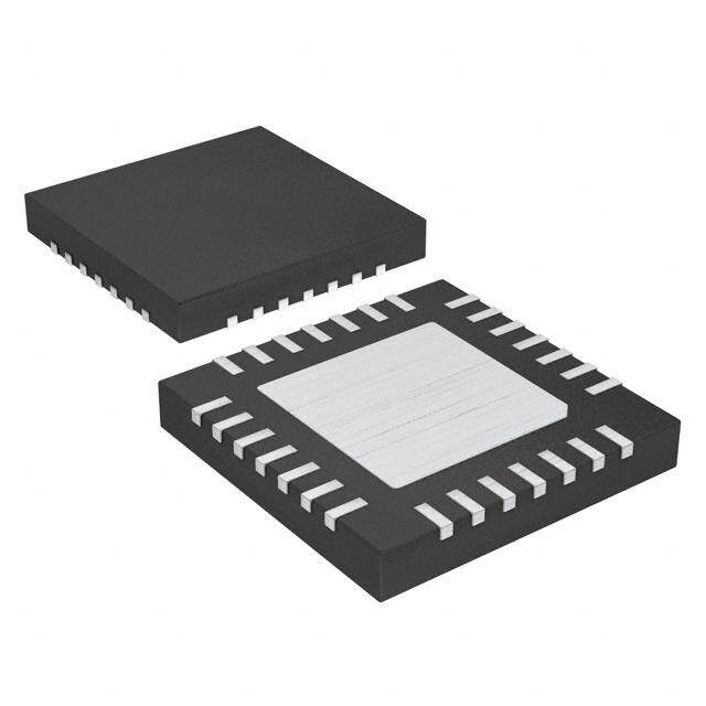
| 供应商器件封装 | 16-QFN-EP(3x3) |
| 其它名称 | LT3756EUD2PBF |
| 内部驱动器 | 无 |
| 包装 | 管件 |
| 安装类型 | 表面贴装 |
| 封装/外壳 | 16-WFQFN 裸露焊盘 |
| 工作温度 | -40°C ~ 125°C |
| 恒压 | 是 |
| 恒流 | 是 |
| 拓扑 | 回扫,低端,PWM,SEPIC,降压(降压),升压(升压) |
| 标准包装 | 121 |
| 电压-电源 | 6 V ~ 100 V |
| 电压-输出 | 100V |
| 类型-初级 | 车载,通用 |
| 类型-次级 | 白色 LED |
| 输出数 | 1 |
| 配用 | /product-detail/zh/DC1319B-B/DC1319B-B-ND/4866546/product-detail/zh/DC1319B-A/DC1319B-A-ND/2185028 |
| 频率 | 100kHz ~ 1MHz |


- 商务部:美国ITC正式对集成电路等产品启动337调查
- 曝三星4nm工艺存在良率问题 高通将骁龙8 Gen1或转产台积电
- 太阳诱电将投资9.5亿元在常州建新厂生产MLCC 预计2023年完工
- 英特尔发布欧洲新工厂建设计划 深化IDM 2.0 战略
- 台积电先进制程称霸业界 有大客户加持明年业绩稳了
- 达到5530亿美元!SIA预计今年全球半导体销售额将创下新高
- 英特尔拟将自动驾驶子公司Mobileye上市 估值或超500亿美元
- 三星加码芯片和SET,合并消费电子和移动部门,撤换高东真等 CEO
- 三星电子宣布重大人事变动 还合并消费电子和移动部门
- 海关总署:前11个月进口集成电路产品价值2.52万亿元 增长14.8%


PDF Datasheet 数据手册内容提取
LT3756/LT3756-1/LT3756-2 100V , 100V IN OUT LED Controller FEATURES DESCRIPTION n 3000:1 True Color PWM™ Dimming The LT®3756, LT3756-1 and LT3756-2 are DC/DC control- n Wide Input Voltage Range: 6V to 100V lers designed to operate as a constant-current source for n Output Voltage Up to 100V driving high current LEDs. They drive a low side external n Constant-Current and Constant-Voltage Regulation N-channel power MOSFET from an internal regulated 7.15V n 100mV High Side Current Sense supply. The fixed frequency, current-mode architecture n Drives LEDs in Boost, Buck Mode, Buck-Boost Mode, results in stable operation over a wide range of supply SEPIC or Flyback Topology and output voltages. A ground referenced voltage FB pin n Adjustable Frequency: 100kHz to 1MHz serves as the input for several LED protection features, n Open LED Protection and also makes it possible for the converter to operate n Programmable Undervoltage Lockout with Hysteresis as a constant-voltage source. A frequency adjust pin n Improved Open LED Status Pin (LT3756-2) allows the user to program the frequency from 100kHz n Frequency Synchronization (LT3756-1) to 1MHz to optimize efficiency, performance or external n PWM Disconnect Switch Driver component size. n CTRL Pin Provides Analog Dimming The LT3756/LT3756-1/LT3756-2 sense output current at n Low Shutdown Current: <1µA the high side of the LED string. High side current sensing n Programmable Soft-Start is the most flexible scheme for driving LEDs, allowing n Thermally Enhanced 16-Lead QFN (3mm × 3mm) boost, buck mode or buck-boost mode configuration. and MSOP Packages The PWM input provides LED dimming ratios of up to n AEC-Q100 Qualified for Automotive Applications 3000:1, and the CTRL input provides additional analog dimming capability. APPLICATIONS All registered trademarks and trademarks are the property of their respective owners. Protected n High Power LED Applications by U.S. patents, including 7199560 and 7321203. n Current Limited Constant Voltage Applications n Battery Charging TYPICAL APPLICATION 94% Efficient 30W White LED Headlamp Driver Efficiency vs V VIN IN 8V TO 60V (100V TRANSIENT) 22µH 100 4.7µF 1M VIN 1M 4.7µF 96 SHDN/UVLO FB 185k 332k VCRTREFL LT3756-2 ISP 0.27Ω 370mA 14k CY (%) 92 INTVC1C00k 40.2k SEGNAISSTNEE EFFICIEN 88 OPENLED 0.018Ω 30W PWM LED 84 SS STRING RT PWMOUT 0.01µF 28.7k VC GNDINTVCC 80 375kHz 0 20 40 60 80 1% 10k INTVCC VIN (V) 0.001µF 4.7µF 375612 TA01b 375612 TA01a Rev. C 1 Document Feedback For more information www.analog.com
LT3756/LT3756-1/LT3756-2 ABSOLUTE MAXIMUM RATINGS (Note 1) V ..........................................................................100V RT ............................................................................1.5V IN SHDN/UVLO ............................................................100V SENSE ......................................................................0.5V ISP, ISN ...................................................................100V Operating Junction Temperature Range (Notes 2, 3) INTV ......................................................V + 0.3V, 8V LT3756E, LT3756I ..............................–40°C to 125°C CC IN GATE, PWMOUT (Note 4) ..........................INTV + 0.3V LT3756H/LT3756J ..............................–40°C to 150°C CC CTRL, PWM, OPENLED .............................................12V Storage Temperature Range ...................–65°C to 150°C VC, V , SS, FB .........................................................3V Lead Temperature (Soldering, 10 sec) REF SYNC ..........................................................................8V MSE ..................................................................300°C PIN CONFIGURATION TOP VIEW L CTR VC ISP ISN TOP VIEW 16 15 14 13 PWMOUT 1 16 GATE VREF 1 12 FB ISFNB 23 1154 SVEINNSE PWM 2 17 11 PWMOUT ISP 4 17 13 INTVCC SYNC OR OPENLED 3 GND 10 GATE VC 5 GND 12 SHDN/UVLO CTRL 6 11 RT SS 4 9 SENSE VREF 7 10 SS 5 6 7 8 PWM 8 9 SYNC OR OPENLED T O C N 16-LEMASDE P PLAACSKTAICG EMSOP R DN/UVL INTVC VI TJMAX = 125°C (E-,I-GRADES), TJMAX = 150°C (H, J-GRADES), θJA = 43°C/W, θJC = 4°C/W SH EXPOSED PAD (PIN 17) IS GND, MUST BE SOLDERED TO PCB UD PACKAGE 16-LEAD (3mm × 3mm) PLASTIC QFN TJMAX = 125°C, θJA = 68°C/W, θJC = 4.2°C/W EXPOSED PAD (PIN 17) IS GND, MUST BE SOLDERED TO PCB ORDER INFORMATION LEAD FREE FINISH TAPE AND REEL PART MARKING* PACKAGE DESCRIPTION TEMPERATURE RANGE LT3756EMSE#PBF LT3756EMSE#TRPBF 3756 16-Lead Plastic MSOP –40°C to 125°C LT3756IMSE#PBF LT3756IMSE#TRPBF 3756 16-Lead Plastic MSOP –40°C to 125°C LT3756EMSE-1#PBF LT3756EMSE-1#TRPBF 37561 16-Lead Plastic MSOP –40°C to 125°C LT3756IMSE-1#PBF LT3756IMSE-1#TRPBF 37561 16-Lead Plastic MSOP –40°C to 125°C LT3756EMSE-2#PBF LT3756EMSE-2#TRPBF 37562 16-Lead Plastic MSOP –40°C to 125°C LT3756IMSE-2#PBF LT3756IMSE-2#TRPBF 37562 16-Lead Plastic MSOP –40°C to 125°C LT3756HMSE-2#PBF LT3756HMSE-2#TRPBF 37562 16-Lead Plastic MSOP –40°C to 150°C LT3756JMSE-2#PBF LT3756JMSE-2#TRPBF 37562 16-Lead Plastic MSOP –40°C to 150°C LT3756EUD#PBF LT3756EUD#TRPBF LDMQ 16-Lead (3mm × 3mm) Plastic QFN –40°C to 125°C LT3756IUD#PBF LT3756IUD#TRPBF LDMQ 16-Lead (3mm × 3mm) Plastic QFN –40°C to 125°C LT3756EUD-1#PBF LT3756EUD-1#TRPBF LDMR 16-Lead (3mm × 3mm) Plastic QFN –40°C to 125°C LT3756IUD-1#PBF LT3756IUD-1#TRPBF LDMR 16-Lead (3mm × 3mm) Plastic QFN –40°C to 125°C LT3756EUD-2#PBF LT3756EUD-2#TRPBF LFKB 16-Lead (3mm × 3mm) Plastic QFN –40°C to 125°C LT3756IUD-2#PBF LT3756IUD-2#TRPBF LFKB 16-Lead (3mm × 3mm) Plastic QFN –40°C to 125°C Rev. C 2 For more information www.analog.com
LT3756/LT3756-1/LT3756-2 ORDER INFORMATION AUTOMOTIVE PRODUCTS** LEAD FREE FINISH TAPE AND REEL PART MARKING* PACKAGE DESCRIPTION TEMPERATURE RANGE LT3756EMSE#WPBF LT3756EMSE#WTRPBF 3756 16-Lead Plastic MSOP –40°C to 125°C LT3756IMSE#WPBF LT3756IMSE#WTRPBF 3756 16-Lead Plastic MSOP –40°C to 125°C LT3756EMSE-1#WPBF LT3756EMSE-1#WTRPBF 37561 16-Lead Plastic MSOP –40°C to 125°C LT3756IMSE-1#WPBF LT3756IMSE-1#WTRPBF 37561 16-Lead Plastic MSOP –40°C to 125°C LT3756EMSE-2#WPBF LT3756EMSE-2#WTRPBF 37562 16-Lead Plastic MSOP –40°C to 125°C LT3756IMSE-2#WPBF LT3756IMSE-2#WTRPBF 37562 16-Lead Plastic MSOP –40°C to 125°C LT3756HMSE-2#WPBF LT3756HMSE-2#WTRPBF 37562 16-Lead Plastic MSOP –40°C to 150°C LT3756JMSE-2#WPBF LT3756JMSE-2#WTRPBF 37562 16-Lead Plastic MSOP –40°C to 150°C Contact the factory for parts specified with wider operating temperature ranges. *The temperature grade is identified by a label on the shipping container. Tape and reel specifications. Some packages are available in 500 unit reels through designated sales channels with #TRMPBF suffix. **Versions of this part are available with controlled manufacturing to support the quality and reliability requirements of automotive applications. These models are designated with a #W suffix. Only the automotive grade products shown are available for use in automotive applications. Contact your local Analog Devices account representative for specific product ordering information and to obtain the specific Automotive Reliability reports for these models. Rev. C 3 For more information www.analog.com
LT3756/LT3756-1/LT3756-2 ELECTRICAL CHARACTERISTICS The l denotes the specifications which apply over the full operating temperature range, otherwise specifications are at T = 25°C. V = 24V, SHDN/UVLO = 24V, CTRL = 2V, PWM = 5V, unless otherwise A IN noted. PARAMETER CONDITIONS MIN TYP MAX UNITS V Minimum Operating Voltage V Tied to INTV l 6 V IN IN CC V Shutdown I SHDN/UVLO = 0V, PWM = 0V 0.1 1 µA IN Q SHDN/UVLO = 1.15V, PWM = 0V 5 µA V Operating I (Not Switching) PWM = 0V 1.4 1.7 mA IN Q V Voltage 100µA ≤ I ≤ 0µA (E, I, H-Grades) l 1.965 2.00 2.045 V REF VREF 80µA ≤ I ≤ 0µA (J-Grade only) l 1.965 2.00 2.045 V VREF V Line Regulation 6V ≤ V ≤ 100V 0.006 %/V REF IN SENSE Current Limit Threshold l 98 108 118 mV SENSE Input Bias Current Current Out of Pin 40 µA SS Pull-Up Current Current Out of Pin 8 10 13 µA Error Amplifier ISP/ISN Full-Scale Current Sense Threshold FB = 0V, ISP = 48V l 96 100 103 mV J-Grade l 95.5 100 103 mV ISP/ISN Current Sense Threshold at CTRL = 0V CTRL = 0V, FB = 0V, ISP = 48V –12 –9.5 –7 mV CTRL Pin Range for Current Sense Threshold Adjustment l 0 1.1 V CTRL Input Bias Current Current Out of Pin 50 100 nA LED Current Sense Amplifier Input Common Mode Range (V ) l 2.9 100 V ISN ISP/ISN Short-Circuit Threshold ISN = 0V 115 150 200 mV ISP/ISN Short-Circuit Fault Sensing Common Mode Range (V ) l 0 3 V ISN ISP/ISN Input Bias Current (Combined) PWM = 5V (Active), ISP = ISN = 48V 55 µA PWM = 0V (Standby), ISP = ISN = 48V 0 0.1 µA LED Current Sense Amplifier g V = 100mV 120 µS m (ISP – ISN) VC Output Impedance 1V < VC < 2V 15000 kΩ VC Standby Input Bias Current PWM = 0V –20 20 nA FB Regulation Voltage (V ) l 1.220 1.250 1.270 V FB ISP = ISN 1.232 1.250 1.265 V J-Grade l 1.215 1.250 1.275 V FB Amplifier g FB = V , ISP = ISN 480 µS m FB FB Pin Input Bias Current Current Out of Pin 40 100 nA FB Open LED Threshold OPENLED Falling V – V – V – V FB FB FB (LT3756 and LT3756-2) 65mV 50mV 40mV FB Overvoltage Threshold PWMOUT Falling V + V + V + V FB FB FB 50mV 60mV 75mV VC Current Mode Gain – (∆VVC/∆VSENSE) 4 V/V Oscillator Switching Frequency R = 100k l 90 100 125 kHz T R = 10k 925 1000 1050 kHz T Minimum Off-Time 170 ns Linear Regulator INTV Regulation Voltage 7 7.15 7.3 V CC Dropout (V – INTV ) I = –10mA, V = 7V 1 V IN CC INTVCC IN INTV Undervoltage Lockout 3.9 4.1 4.3 V CC Rev. C 4 For more information www.analog.com
LT3756/LT3756-1/LT3756-2 ELECTRICAL CHARACTERISTICS The l denotes the specifications which apply over the full operating temperature range, otherwise specifications are at T = 25°C. V = 24V, SHDN/UVLO = 24V, CTRL = 2V, PWM = 5V, unless otherwise A IN noted. PARAMETER CONDITIONS MIN TYP MAX UNITS INTV Current Limit 14 17 23 mA CC INTV Current in Shutdown SHDN/UVLO = 0V, INTV = 7V 8 12 µA CC CC Logic Inputs/Outputs PWM Input High Voltage l 1.5 V PWM Input Low Voltage l 0.4 V PWM Pin Resistance to GND 45 60 kΩ PWMOUT Output Low (V ) 0 50 mV OL PWMOUT Output High (V ) INTV – V OH CC 0.05 SHDN/UVLO Threshold Voltage Falling E-, I-Grades l 1.185 1.220 1.245 V H Grade l 1.175 1.245 V J-Grade l 1.159 1.260 V SHDN/UVLO Rising Hysteresis 20 mV SHDN/UVLO Input Low Voltage I Drops Below 1µA 0.4 V VIN SHDN/UVLO Pin Bias Current Low SHDN/UVLO = 1.15V 1.7 2.05 2.5 µA SHDN/UVLO Pin Bias Current High SHDN/UVLO = 1.30V 10 100 nA OPENLED Output Low (V ) I = 0.5mA 200 mV OL OPENLED (LT3756 and LT3756-2) SYNC Pin Resistance to GND LT3756-1 Only 30 kΩ SYNC Input High LT3756-1 Only 1.5 V SYNC Input Low LT3756-1 Only 0.4 V Gate Driver t GATE Driver Output Rise Time C = 3300pF 35 ns r L t GATE Driver Output Fall Time C = 3300pF 35 ns f L GATE Output Low (V ) 0.05 V OL GATE Output High (V ) INTV – V OH CC 0.05 Note 1: Stresses beyond those listed under Absolute Maximum Ratings Note 3: The LT3756 includes overtemperature protection that is intended may cause permanent damage to the device. Exposure to any Absolute to protect the device during momentary overload conditions. Junction Maximum Rating condition for extended periods may affect device temperature will exceed the maximum operating junction temperature reliability and lifetime. when overtemperature protection is active. Continuous operating above Note 2: The LT3756E, LT3756E-1 and LT3756E-2 are guaranteed to meet the specified maximum operating junction temperature may impair device performance specifications from 0°C to 125°C junction temperature. reliability. Specifications over the –40°C to 125°C operating junction temperature Note 4: GATE and PWMOUT pins are driven either to GND or INTV by CC range are assured by design, characterization and correlation with internal switches. Do not connect these pins externally to a power supply. statistical process controls. The LT3756I, LT3756I-1 and LT3756I-2 are guaranteed to meet performance specifications over the –40°C to 125°C operating junction temperature range. The LT3756H-2 and LT3755J-2 are guaranteed to meet performance specifications over the full –40°C to 150°C operating junction temperature range. High junction temperatures degrade operating lifetimes. Operating lifetime is derated at junction temperatures greater than 125°C. Rev. C 5 For more information www.analog.com
LT3756/LT3756-1/LT3756-2 TYPICAL PERFORMANCE CHARACTERISTICS T = 25°C, unless otherwise noted. A V Threshold (ISP – ISN) V Threshold vs V V Threshold vs V vs Temperature (ISP – ISN) CTRL (ISP – ISN) ISP 120 103 103 VCTRL = 2V VCTRL = 2V 100 102 102 V) V) V) m m m LD ( 80 LD ( 101 LD ( 101 O O O SH 60 SH SH E E E R R 100 R 100 H H H TN) 40 TN) TN) P – IS 20 P – IS 99 P – IS 99 S S S V(I V(I 98 V(I 98 0 –20 97 97 0 0.5 1 1.5 2 0 20 40 60 80 100 –50 –25 0 25 50 75 100 125 150 VCTRL (V) ISP VOLTAGE (V) TEMPERATURE (°C) 375612 G01 375612 G02 375612 G03 FB Regulation Voltage vs Temperature V Voltage vs Temperature V Voltage vs V REF REF IN 1.28 2.04 2.04 1.27 2.03 2.03 1.26 2.02 2.02 1.25 2.01 2.01 V (V)FB1.24 V (V)REF2.00 V (V)REF2.00 1.23 1.99 1.99 1.22 1.98 1.98 1.21 1.97 1.97 1.20 1.96 1.96 –50 –25 0 25 50 75 100 125 150 –50 –25 0 25 50 75 100 125 150 0 20 40 60 80 100 TEMPERATURE (°C) TEMPERATURE (°C) VIN (V) 375612 G04 375612 G05 375612 G06 Switching Frequency SHDN/UVLO Hysteresis Current Switching Frequency vs R vs Temperature vs Temperature T 10000 500 2.4 RT = 26.7k EQUENCY (kHz)1000 EQUENCY (kHz) 440500 (µA)VLO22..20 R R U G F G F DN/ N N H HI 100 HI IS C C WIT WIT 350 1.8 S S 10 300 1.6 10 100 –50 –25 0 25 50 75 100 125 150 –50 –25 0 25 50 75 100 125 150 RT (k) TEMPERATURE (°C) TEMPERATURE (°C) 375612 G07 375612 G08 375612 G09 Rev. C 6 For more information www.analog.com
LT3756/LT3756-1/LT3756-2 TYPICAL PERFORMANCE CHARACTERISTICS T = 25°C, unless otherwise noted. A SENSE Current Limit Threshold SHDN/UVLO Threshold Quiescent Current vs V vs Temperature vs Temperature IN 2.0 110 1.28 PWM = 0V 1.26 1.5 V) 105 V) NT (mA) HOLD (m OLTAGE (1.24 SHDN/UVLO RISING V CURREIN1.0 NSE THRES 100 DN/UVLO V 1.22 SHDN/UVLO FALLING 0.5 SE 95 SH 1.20 0 90 1.18 0 20 40 60 80 100 –50 –25 0 25 50 75 100 125 150 –50 –25 0 25 50 75 100 125 150 VIN (V) TEMPERATURE (°C) TEMPERATURE (°C) 375612 G10 375612 G11 375612 G12 INTV Current Limit CC INTV Voltage vs V vs Temperature INTV Voltage vs Temperature CC IN CC 8 20 7.4 A) 18 6 m 7.3 T ( MI V (V)INTVCC 4 CURRENT LI 1164 INTV (V)CC 7.2 C C 2 TV 7.1 N 12 I 0 10 7.0 0 20 40 60 80 100 –50 –25 0 25 50 75 100 125 150 –50 –25 0 25 50 75 100 125 150 VIN (V) TEMPERATURE (°C) TEMPERATURE (°C) 375612 G13 375612 G14 375612 G15 SENSE Current Limit Threshold Gate Rise/Fall Time vs Duty Cycle V Threshold vs FB Voltage vs Capacitance (ISP-ISN) 110 125 100 VCTRL = 2V 10% TO 90% V) 100 80 mV)105 D (m GATE RISE D ( OL TIME THRESHOL100 THRESHN) 7550 TIME (ns) 6400 FALGLA TTEIME SENSE 95 V(ISP – IS 25 20 90 0 0 0 25 50 75 100 1.2 1.22 1.24 1.26 1.28 0 2 4 6 8 10 DUTY CYCLE (%) FB VOLTAGE (V) CAPACITANCE (nF) 375612 G16 375612 G17 375612 G18 Rev. C 7 For more information www.analog.com
LT3756/LT3756-1/LT3756-2 TYPICAL PERFORMANCE CHARACTERISTICS T = 25°C, unless otherwise noted. A ISP/ISN Input Bias Current INTV Dropout Voltage CC vs CTRL Voltage vs Current, Temperature 40 0 ISP µA) 30 –0.5 –45°C RENT ( ISN UT (V) –1.0 CUR 20 OPO 25°C S R BIA O D –1.5 NPUT 10 LD 150°C 125°C I –2.0 VIN = 7V 0 –2.5 0 0.5 1 1.5 2 0 3 6 9 12 15 CTRL (V) LDO CURRENT (mA) 375612 G19 375612 G20 PIN FUNCTIONS (MSOP/QFN) PWMOUT (Pin 1/Pin 11): Buffered Version of PWM Signal ISN (Pin 3/Pin 13): Connection Point for the Negative for Driving LED Load Disconnect NMOS or Level Shift. Terminal of the Current Feedback Resistor. If ISN is greater This pin also serves in a protection function for the FB than 2.9V, the LED current can be programmed by I = LED overvoltage condition—will toggle if the FB input is greater 100mV/R when V > 1.2V or I = (V –100mV)/ LED CTRL LED CTRL than the FB regulation voltage (V ) plus 60mV (typical). (10 • R ) when V ≤ 1V. Input bias current is typi- FB LED CTRL The PWMOUT pin is driven from INTV . Use of a FET with cally 25µA. Below 3V, ISN is an input to the short-circuit CC gate cut-off voltage higher than 1V is recommended. protection feature that forces GATE to 0V if ISP exceeds ISN by more than 150mV (typ). FB (Pin 2/Pin 12): Voltage Loop Feedback Pin. FB is intended for constant-voltage regulation or for LED protec- ISP (Pin 4/Pin 14): Connection Point for the Positive tion/open LED detection. The internal transconductance Terminal of the Current Feedback Resistor. Input bias amplifier with output VC will regulate FB to 1.25V (nominal) current is dependent upon CTRL pin voltage as shown through the DC/DC converter. If the FB input is regulating in the TPC. ISP is an input to the short-circuit protection the loop, the OPENLED pull-down is asserted. This ac- feature when ISN is less than 3V. tion may signal an open LED fault. If FB is driven above VC (Pin 5/Pin 15): Transconductance Error Amplifier the FB threshold (by an external power supply spike, for Output Pin Used to Stabilize the Voltage Loop with an RC example), the OPENLED pull-down will be de-asserted and Network. This pin is high impedance when PWM is low, a the PWMOUT pin will be driven low to protect the LEDs feature that stores the demand current state variable for from an overcurrent event. Do not leave the FB pin open. the next PWM high transition. Connect a capacitor between If not used, connect to GND. this pin and GND; a resistor in series with the capacitor is recommended for fast transient response. Rev. C 8 For more information www.analog.com
LT3756/LT3756-1/LT3756-2 PIN FUNCTIONS CTRL (Pin 6/Pin 16): Current Sense Threshold Adjustment by an undervoltage condition (detected by SHDN/UVLO Pin. Regulating threshold V is 1/10th V plus pin) or thermal limit. (ISP – ISN) CTRL an offset for 0V < V < 1V. For V > 1.2V the current CTRL CTRL RT (Pin 11/Pin 5): Switching Frequency Adjustment Pin. sense threshold is constant at the full-scale value of 100mV. Set the frequency using a resistor to GND (for resistor For 1V < V < 1.2V, the dependence of current sense CTRL values, see the Typical Performance curve or Table 1). threshold upon V transitions from a linear function CTRL Do not leave the RT pin open. to a constant value, reaching 98% of full-scale value by SHDN/UVLO (Pin 12/Pin 6): Shutdown and Undervoltage V = 1.1V. Do not leave this pin open. CTRL Detect Pin. An accurate 1.22V falling threshold with ex- V (Pin 7/Pin 1): Voltage Reference Output Pin, Typically REF ternally programmable hysteresis detects when power is 2V. This pin drives a resistor divider for the CTRL pin, either OK to enable switching. Rising hysteresis is generated for analog dimming or for temperature limit/compensation by the external resistor divider and an accurate internal of LED load. Can supply up to 100μA. 2.1µA pull-down current. Above the threshold (but below PWM (Pin 8/Pin 2): A signal low turns off switcher, idles 6V), SHDN/UVLO input bias current is sub-µA. Below the oscillator and disconnects VC pin from all internal loads. falling threshold, a 2.1µA pull-down current is enabled so PWMOUT pin follows PWM pin. PWM has an internal the user can define the hysteresis with the external resis- pull-down resistor. If not used, connect to INTV . tor selection. An undervoltage condition resets soft-start. CC Tie to 0.4V, or less, to disable the device and reduce V OPENLED (Pin 9/Pin 3, LT3756 and LT3756-2): An open- IN quiescent current below 1µA. collector pull-down on OPENLED asserts if the FB input is greater than the FB regulation threshold minus 50mV INTV (Pin 13/Pin 7): Regulated Supply for Internal CC (typical). To function, the pin requires an external pull-up Loads, GATE Driver and PWMOUT Driver. Supplied from current less than 1mA. When the PWM input is low and V and regulates to 7.15V (typical). INTV must be IN CC the DC/DC converter is idle, the OPENLED condition is bypassed with a 4.7µF capacitor placed close to the pin. latched to the last valid state when the PWM input was Connect INTV directly to V if V is always less than CC IN IN high. When PWM input goes high again, the OPENLED or equal to 8V. pin will be updated. This pin may be used to report an V (Pin 14/Pin 8): Input Supply Pin. Must be locally open LED fault. IN bypassed with a 0.22µF (or larger) capacitor placed close SYNC (Pin 9/Pin 3, LT3756-1 Only): The SYNC pin is used to the IC. to synchronize the internal oscillator to an external logic SENSE (Pin 15/Pin 9): The current sense input for the level signal. The R resistor should be chosen to program T control loop. Kelvin connect this pin to the positive ter- an internal switching frequency 20% slower than the SYNC minal of the switch current sense resistor, R , in the pulse frequency. Gate turn-on occurs a fixed delay after SENSE source of the NFET. The negative terminal of the current the rising edge of SYNC. For best PWM performance, the sense resistor should be connected to the GND plane PWM rising edge should occur at least 200ns before the close to the IC. SYNC rising edge. Use a 50% duty cycle waveform to drive this pin. This pin replaces OPENLED on LT3756-1 option GATE (Pin 16/Pin 10): N-channel FET Gate Driver Output. parts. If not used, tie this pin to GND. Switches between INTV and GND. Driven to GND during CC shutdown, fault or idle states. SS (Pin 10/Pin 4): Soft-Start Pin. This pin modulates oscillator frequency and compensation pin voltage (VC) GND (Pin 17/Pin 17): Ground. This pin also serves as clamp. The soft-start interval is set with an external capaci- current sense input for control loop, sensing negative tor. The pin has a 10µA (typical) pull-up current source terminal of current sense resistor. Solder the exposed pad to an internal 2.5V rail. The soft-start pin is reset to GND directly to ground plane. Rev. C 9 For more information www.analog.com
LT3756/LT3756-1/LT3756-2 BLOCK DIAGRAM SHDN/UVLO – A6 FB VC PWMOUT PWM VIN – SHDN 1.22V + 1.3V + LDO 2.1µA OVFB 1.25V – COMPARATOR A8 + 7.15V INTVCC A5 + 1.25V –gm 1FB0µ =A 1 A.2T5V SHORT-CIRCUIT DETECT SCILMB + 10µA –+ 150mV –A10 SCILMB + R Q GATE IISSPN 5k +–A1EAgMmP 1A01µ+ A= AAT1– –CAO2MPPWARMATOR S IDSERNIVSEER+ SENSE CTRL A4 CTRL + BUFFER – 1.1V +A3 Q2 GND – VC RAMP GENERATOR SSCLAMP 50k 100kHz TO 1MHz OSCILLATOR OPENLED FAULT 10µA VREF 140µA LOGIC 1.25V ++– 1.2FVB +– (ALNTD3756 – TLIM FREQ LT3756-2) A7 170k 165°C PROG 2V + SS RT SYNC (LT3756-1 ONLY) 375612 BD Rev. C 10 For more information www.analog.com
LT3756/LT3756-1/LT3756-2 OPERATION The LT3756 is a constant-frequency, current mode control- difference between ISP and ISN is monitored to determine ler with a low side NMOS gate driver. The GATE pin and if the output is in a short-circuit condition. If the difference PWMOUT pin drivers, and other chip loads, are powered between ISP and ISN is greater than 150mV (typical), the from INTV , which is an internally regulated supply. In SR latch will be reset regardless of the PWM comparator. CC the discussion that follows, it will be helpful to refer to These functions are intended to protect the power switch, the Block Diagram of the IC. In normal operation, with the as well as various external components in the power path PWM pin low, the GATE and PWMOUT pins are driven to of the DC/DC converter. GND, the VC pin is high impedance to store the previous In voltage feedback mode, the operation is similar to that switching state on the external compensation capacitor, described above, except the voltage at the VC pin is set and the ISP and ISN pin bias currents are reduced to by the amplified difference of the internal reference of leakage levels. When the PWM pin transitions high, the 1.25V (nominal) and the FB pin. If FB is lower than the PWMOUT pin transitions high after a short delay. At the reference voltage, the switch current will increase; if FB same time, the internal oscillator wakes up and gener- is higher than the reference voltage, the switch demand ates a pulse to set the PWM latch, turning on the external current will decrease. The LED current sense feedback power MOSFET switch (GATE goes high). A voltage input interacts with the FB voltage feedback so that FB will not proportional to the switch current, sensed by an external exceed the internal reference and the voltage between ISP current sense resistor between the SENSE and GND input and ISN will not exceed the threshold set by the CTRL pin. pins, is added to a stabilizing slope compensation ramp For accurate current or voltage regulation, it is necessary and the resulting “switch current sense” signal is fed into to be sure that under normal operating conditions, the the positive terminal of the PWM comparator. The current appropriate loop is dominant. To deactivate the voltage in the external inductor increases steadily during the time loop entirely, FB can be connected to GND. To deactivate the switch is on. When the switch current sense voltage the LED current loop entirely, the ISP and ISN should be exceeds the output of the error amplifier, labeled “VC”, tied together and the CTRL input tied to V . REF the latch is reset and the switch is turned off. During the switch off phase, the inductor current decreases. At the Two LED specific functions featured on the LT3756 are completion of each oscillator cycle, internal signals such controlled by the voltage feedback pin. First, when the as slope compensation return to their starting points and a FB pin exceeds a voltage 50mV lower (–4%) than the FB new cycle begins with the set pulse from the oscillator. regulation voltage, the pull-down driver on the OPENLED pin is activated (LT3756 and LT3756-2 only). This function Through this repetitive action, the PWM control algorithm provides a status indicator that the load may be discon- establishes a switch duty cycle to regulate a current or nected and the constant-voltage feedback loop is taking voltage in the load. The VC signal is integrated over many control of the switching regulator. When the FB pin exceeds switching cycles and is an amplified version of the differ- the FB regulation voltage by 60mV (5% typical), the PWM- ence between the LED current sense voltage, measured OUT pin is driven low, ignoring the state of the PWM input. between ISP and ISN, and the target difference voltage In the case where the PWMOUT pin drives a disconnect set by the CTRL pin. In this manner, the error amplifier NFET, this action isolates the LED load from GND, prevent- sets the correct peak switch current level to keep the ing excessive current from damaging the LEDs. If the FB LED current in regulation. If the error amplifier output input exceeds both the open LED and the overvoltage increases, more current is demanded in the switch; if it thresholds, then an externally driven overvoltage event decreases, less current is demanded. The switch current has caused the FB pin to be too high and the OPENLED is monitored during the on-phase and the voltage across pull-down will be de-asserted. The LT3756-2 will re-assert the SENSE pin is not allowed to exceed the current limit the OPENLED signal when FB falls below the overvoltage threshold of 108mV (typical). If the SENSE pin exceeds threshold and remains above the open LED threshold. The the current limit threshold, the SR latch is reset regard- LT3756 is prevented from re-asserting OPENLED until FB less of the output state of the PWM comparator. Likewise, drops below both thresholds. at an ISP/ISN common mode voltage less than 3V, the Rev. C 11 For more information www.analog.com
LT3756/LT3756-1/LT3756-2 APPLICATIONS INFORMATION INTV Regulator Bypassing and Operation The following equations should be used to determine the CC values of the resistors: The INTV pin requires a capacitor for stable operation CC and to store the charge for the large GATE switching cur- R1+R2 V =1.22• rents. Choose a 10V rated low ESR, X7R or X5R ceramic IN,FALLING R2 capacitor for best performance. A 4.7µF capacitor will be adequate for many applications. Place the capacitor close V = 2.1µA•R1+ V IN,RISING IN,FALLING to the IC to minimize the trace length to the INTV pin CC and also to the IC ground. VIN An internal current limit on the INTVCC output protects LT3756 R1 the LT3756 from excessive on-chip power dissipation. SHDN/UVLO The minimum value of this current should be considered R2 when choosing the switching NMOS and the operating 375612 F01 frequency. Figure 1. Resistor Connection to Set V IN I can be calculated from the following equation: Undervoltage Shutdown Threshold INTVCC I = Q • f INTVCC G OSC LED Current Programming Careful choice of a lower Q FET will allow higher switch- G The LED current is programmed by placing an appropriate ing frequencies, leading to smaller magnetics. The INTV CC value current sense resistor, R , in series with the LED LED pin has its own undervoltage disable (UVLO) set to 4.1V string. The voltage drop across R is (Kelvin) sensed LED (typical) to protect the external FETs from excessive power by the ISP and ISN pins. Typically, sensing of the current dissipation caused by not being fully enhanced. If the should be done at the top of the LED string. If this option INTV pin drops below the UVLO threshold, the GATE CC is not available, then the current may be sensed at the and PWMOUT pins will be forced to 0V and the soft-start bottom of the string, but take caution that the minimum pin will be reset. ISN value does not fall below 3V, which is the lower limit of If the input voltage, V , will not exceed 8V, then the INTV the LED current regulation function. The CTRL pin should IN CC pin could be connected to the input supply. Be aware that be tied to a voltage higher than 1.1V to get the full-scale a small current (less than 12μA) will load the INTV in 100mV (typical) threshold across the sense resistor. The CC shutdown. If V is normally above, but occasionally drops CTRL pin can also be used to dim the LED current to zero, IN below the INTV regulation voltage, then the minimum although relative accuracy decreases with the decreasing CC operating V will be close to 7V . This value is determined voltage sense threshold. When the CTRL pin voltage is IN by the dropout voltage of the linear regulator and the 4.5V less than 1.0V, the LED current is: (4.1V typical) INTVCC undervoltage lockout threshold VCTRL −100mV mentioned above. ILED = R •10 LED Programming the Turn-On and Turn-Off Thresholds When the CTRL pin voltage is between 1V and 1.2V the LED with the SHDN/UVLO Pin current varies with CTRL, but departs from the equation The falling UVLO value can be accurately set by the resistor above by an increasing amount as CTRL voltage increases. divider. A small 2.1µA pull-down current is active when Ultimately, above CTRL = 1.2V the LED current no longer SHDN/UVLO is below the threshold. The purpose of this varies with CTRL. At CTRL = 1.1V, the actual value of I LED current is to allow the user to program the rising hysteresis. is ~98% of the equation’s estimate. Rev. C 12 For more information www.analog.com
LT3756/LT3756-1/LT3756-2 APPLICATIONS INFORMATION When V is higher than 1.2V, the LED current is regu- normal operation will not exceed 1.1V. For an LED driver CTRL lated to: of buck or a buck-boost configuration, the output voltage is typically level-shifted to a signal with respect to GND 100mV I = as illustrated in Figure 3. The output can be expressed as: LED R LED R3 V = V +1.25• The LED current programming feature can increase total OUT BE R4 dimming range by a factor of 10. The CTRL pin should not be left open (tie to V if not used). The CTRL pin REF + can also be used in conjunction with a thermistor to R3 RSEN(EXT) provide overtemperature protection for the LED load, or VOUT LED COUT with a resistor divider to V to reduce output power and ARRAY IN – 100k LT3756 switching current when V is low. The presence of a time IN varying differential voltage signal (ripple) across ISP and FB R4 ISN at the switching frequency is expected. The amplitude 375612 F03 of this signal is increased by high LED load current, low switching frequency and/or a smaller value output filter Figure 3. Feedback Resistor Connection for capacitor. Some level of ripple signal is acceptable: the Buck Mode or Buck-Boost Mode LED Driver compensation capacitor on the VC pin filters the signal so the average difference between ISP and ISN is regulated ISP/ISN Short-Circuit Protection Feature (for SEPIC) to the user-programmed value. Ripple voltage amplitude The ISP and ISN pins have a protection feature indepen- (peak-to-peak) in excess of 20mV should not cause mis- dent of the LED current sense feature that operates at operation, but may lead to noticeable offset between the ISN below 3V. The purpose of this feature is to provide average value and the user-programmed value. continuous current sensing when ISN is below the LED Programming Output Voltage (Constant-Voltage current sense common mode range (during start-up or Regulation) or Open LED/Overvoltage Threshold an output short-circuit fault) to prevent the development of excessive switching currents that could damage the For a boost or SEPIC application, the output voltage can power components in a SEPIC converter. The action be set by selecting the values of R3 and R4 (see Figure 2) threshold (150mV, typ) is above the default LED current according to the following equation: sense threshold, so that no interference will occur over R3+R4 the ISN voltage range where these two functions overlap. V =1.25• OUT R4 This feature acts in the same manner as SENSE current limit—it prevents GATE from going high (switch turn-on) For a boost type LED driver, set the resistor from the until the ISP/ISN difference falls below the threshold. If the output to the FB pin such that the expected V during FB load has appreciable series inductance, use of a Schottky clamp from GND to ISN is recommended for the SEPIC VIN to prevent excessive current flowing from the ISN pin in LT3756 a fault. R3 FB Dimming Control R4 375612 F02 There are two methods to control the current source for dimming using the LT3756. One method uses the CTRL Figure 2. Feedback Resistor Connection for Boost or SEPIC LED Drivers pin to adjust the current regulated in the LEDs. A second Rev. C 13 For more information www.analog.com
LT3756/LT3756-1/LT3756-2 APPLICATIONS INFORMATION Duty Cycle Considerations method uses the PWM pin to modulate the current source between zero and full current to achieve a precisely pro- Switching duty cycle is a key variable defining converter grammed average current. To make PWM dimming more operation, therefore, its limits must be considered when accurate, the switch demand current is stored on the VC programming the switching frequency for a particular node during the quiescent phase when PWM is low. This application. The fixed minimum on-time and minimum feature minimizes recovery time when the PWM signal goes off-time (see Figure 4) and the switching frequency define high. To further improve the recovery time, a disconnect the minimum and maximum duty cycle of the switch, re- switch may be used in the LED current path to prevent the spectively. The following equations express the minimum/ ISP node from discharging during the PWM signal low maximum duty cycle: phase. The minimum PWM on or off time will depend on Min Duty Cycle = (minimum on-time) • switching fre- the choice of operating frequency and external component quency selection. With operation in discontinuous conduction mode (DCM), regulated current pulses as short as 1µs are Max Duty Cycle = 1 – (minimum off-time) • switching achievable. But, the best overall combination of PWM and frequency analog dimming (with CTRL) is available if the minimum When calculating the operating limits, the typical values PWM pulse is at least six switching cycles. for on/off-time in the data sheet should be increased by at least 60ns to allow margin for PWM control latitude, Programming the Switching Frequency GATE rise/fall times and SW node rise/fall times. The RT frequency adjust pin allows the user to program the switching frequency from 100kHz to 1MHz to optimize 300 CGATE = 3300pF efficiency/performance or external component size. Higher 250 frequency operation yields smaller component size but MINIMUM ON-TIME increases switching losses and gate driving current, and 200 may not allow sufficiently high or low duty cycle operation. s) MINIMUM OFF-TIME n Lower frequency operation gives better performance at the E ( 150 M TI cost of larger external component size. For an appropriate 100 R resistor value see Table 1. An external resistor from the T RT pin to GND is required—do not leave this pin open. 50 Table 1. Switching Frequency vs R Value 0 T –50 –25 0 25 50 75 100 125 150 fOSC (kHz) RT (kΩ) TEMPERATURE (°C) 375612 F04 1000 10.0 Figure 4. Typical Minimum On and Off 900 11.8 Pulse Width vs Temperature 800 13.0 700 15.4 600 17.8 Thermal Considerations 500 21.0 The LT3756 series is rated to a maximum input voltage of 400 26.7 100V. Careful attention must be paid to the internal power 300 35.7 dissipation of the IC at higher input voltages to ensure that 200 53.6 a junction temperature of 125°C (150°C for H-grade and 100 100 J-Grade) is not exceeded. This junction limit is especially Rev. C 14 For more information www.analog.com
LT3756/LT3756-1/LT3756-2 APPLICATIONS INFORMATION important when operating at high ambient temperatures. Driving SYNC with a 50% duty cycle waveform is always The majority of the power dissipation in the IC comes from a good choice, otherwise, maintain the duty cycle between the supply current needed to drive the gate capacitance of 20% and 60%. When using both PWM and SYNC features, the external power MOSFET. This gate drive current can the PWM signal rising edge should occur at least 200ns be calculated as: before the SYNC rising edge (V ) for optimal PWM IH performance. If the SYNC pin is not used, it should be I = f • Q GATE SW G connected to GND. A low Q power MOSFET should always be used when op- G erating at high input voltages, and the switching frequency Open LED Detection (LT3756 and LT3756-2) should also be chosen carefully to ensure that the IC does The LT3756 and LT3756-2 provide an open-collector status not exceed a safe junction temperature. The internal junc- pin, OPENLED, that pulls low when the FB pin is within tion temperature of the IC can be estimated by: ~50mV of its 1.25V regulated voltage. If the open LED T = T + [V (I + f • Q ) • θ ] clamp voltage is programmed correctly using the FB pin, J A IN Q SW G JA then the FB pin should never exceed 1.1V when LEDs are where T is the ambient temperature, I is the quiescent A Q connected, therefore, the only way for the FB pin to be current of the part (maximum 1.5mA) and θ is the JA within 50mV of the regulation voltage is for an open LED package thermal impedance (68°C/W for the 3mm × 3mm event to have occurred. The key difference between the QFN package). For example, an application with T A(MAX) LT3756 and LT3756-2 is the behavior of the OPENLED pin = 85°C, V = 60V, f = 400kHz, and having a FET IN(MAX) SW when the FB pin crosses and re-crosses the FB overvoltage with Q = 20nC, the maximum IC junction temperature G threshold at 1.31V (typ). The LT3756-2 asserts/de-asserts will be approximately: OPENLED freely when crossing the 1.31V threshold. T = 85°C + [60V (1.5mA + 400kHz • 20nC) • 68°C/W] J The LT3756, by comparison, de-asserts OPENLED when = 124°C FB exceeds 1.31V and is prevented from re-asserting The exposed pad on the bottom of the package must be OPENLED until the FB pin falls below the 1.2V (typ) open soldered to a ground plane. This ground should then be LED threshold and clears the fault. The LT3756-2 has the connected to an internal copper ground plane with thermal more general purpose behavior and is recommended for vias placed directly under the package to spread out the applications using OPENLED. heat dissipated by the IC. Input Capacitor Selection If LT3756 junction temperature reaches 165°C, the GATE The input capacitor supplies the transient input current for and PWMOUT pins will be driven to GND and the soft- the power inductor of the converter and must be placed start (SS) pin will be discharged to GND. Switching will and sized according to the transient current requirements. be enabled after device temperature is reduced 10°C. This The switching frequency, output current and tolerable input function is intended to protect the device during momentary thermal overload conditions. voltage ripple are key inputs to estimating the capacitor value. An X7R type ceramic capacitor is usually the best Frequency Synchronization (LT3756-1 Only) choice since it has the least variation with temperature and DC bias. Typically, boost and SEPIC converters re- The LT3756-1 switching frequency can be synchronized to quire a lower value capacitor than a buck mode converter. an external clock using the SYNC pin. For proper operation, Assuming that a 100mV input voltage ripple is acceptable, the R resistor should be chosen for a switching frequency T the required capacitor value for a boost converter can be 20% lower than the external clock frequency. The SYNC estimated as follows: pin is disabled during the soft-start period. V 1µF Observation of the following guidelines about the SYNC C (µF)=I (A)• OUT •t (µs)• IN LED SW V A•µs waveform will ensure proper operation of this feature. IN Rev. C 15 For more information www.analog.com
LT3756/LT3756-1/LT3756-2 APPLICATIONS INFORMATION Therefore, a 4.7µF capacitor is an appropriate selection operating frequencies will require proportionately higher for a 400kHz boost regulator with 12V input, 48V output capacitor values. and 1A load. Soft-Start Capacitor Selection With the same V voltage ripple of 100mV, the input capaci- IN tor for a buck converter can be estimated as follows: For many applications, it is important to minimize the inrush current at start-up. The built-in soft-start circuit 4.7µF C (µF)=I (A)•t (µs)• significantly reduces the start-up current spike and output IN LED SW A•µs voltage overshoot. The soft-start interval is set by the soft- start capacitor selection according to the equation: A 10µF input capacitor is an appropriate selection for a 400kHz buck mode converter with a 1A load. 2V T = C • SS SS In the buck mode configuration, the input capacitor has 10µA large pulsed currents due to the current returned through A typical value for the soft-start capacitor is 0.01µF. The the Schottky diode when the switch is off. In this buck soft-start pin reduces the oscillator frequency and the converter case it is important to place the capacitor as close maximum current in the switch. The soft-start capacitor as possible to the Schottky diode and to the GND return is discharged when SHDN/UVLO falls below its threshold, of the switch (i.e., the sense resistor). It is also important during an overtemperature event or during an INTV CC to consider the ripple current rating of the capacitor. For undervoltage event. During start-up with SHDN/UVLO, best reliability, this capacitor should have low ESR and charging of the soft-start capacitor is enabled after the ESL and have an adequate ripple current rating. The RMS first PWM high period. input current for a buck mode LED driver is: Power MOSFET Selection I =I • (1–D)•D IN(RMS) LED For applications operating at high input or output voltages, where D is the switch duty cycle. the power NMOS FET switch is typically chosen for drain voltage V rating and low gate charge Q . Consideration DS G Table 2. Recommended Ceramic Capacitor Manufacturers of switch on-resistance, R , is usually secondary be- DS(ON) MANUFACTURER WEB cause switching losses dominate power loss. The INTV CC TDK www.tdk.com regulator on the LT3756 has a fixed current limit to protect Kemet www.kemet.com the IC from excessive power dissipation at high V , so the IN Murata www.murata.com FET should be chosen so that the product of Q at 7V and G Taiyo Yuden www.t-yuden.com switching frequency does not exceed the INTV current CC limit. For driving LEDs be careful to choose a switch with Output Capacitor Selection a V rating that exceeds the threshold set by the FB pin DS The selection of the output capacitor depends on the load in case of an open-load fault. Several MOSFET vendors and converter configuration, i.e., step-up or step-down are listed in Table 3. The MOSFETs used in the application and the operating frequency. For LED applications, the circuits in this data sheet have been found to work well equivalent resistance of the LED is typically low and the with the LT3756. Consult factory applications for other output filter capacitor should be sized to attenuate the recommended MOSFETs. current ripple. Use of an X7R type ceramic capacitor is Table 3. MOSFET Manufacturers recommended. VENDOR WEB To achieve the same LED ripple current, the required filter Vishay Siliconix www.vishay.com capacitor is larger in the boost and buck-boost mode ap- Fairchild www.fairchildsemi.com plications than that in the buck mode applications. Lower International Rectifier www.irf.com Rev. C 16 For more information www.analog.com
LT3756/LT3756-1/LT3756-2 APPLICATIONS INFORMATION Schottky Rectifier Selection These equations provide an estimate of the sense resistor value based on reasonable assumptions about induc- The power Schottky diode conducts current during the tor current ripple during steady state switching. Lower interval when the switch is turned off. Select a diode rated values of sense resistor may be required in applications for the maximum SW voltage. If using the PWM feature for where inductor ripple current is higher. Examples include dimming, it is important to consider diode leakage, which applications with current limited operation at high duty increases with the temperature, from the output during the cycle, and those with discontinuous conduction mode PWM low interval. Therefore, choose the Schottky diode (DCM) switching. It is always prudent to verify the peak with sufficiently low leakage current. Table 4 has some inductor current in the application to ensure the sense recommended component vendors. resistor selection provides margin to the SENSE current Table 4. Schottky Rectifier Manufacturers limit threshold. VENDOR WEB Inductor Selection On Semiconductor www.onsemi.com Diodes, Inc. www.diodes.com The inductor used with the LT3756 should have a saturation Central Semiconductor www.centralsemi.com current rating appropriate to the maximum switch current selected with the R resistor. Choose an inductor value SENSE Sense Resistor Selection based on operating frequency, input and output voltage to The resistor, R , between the source of the exter- provide a current mode ramp on SENSE during the switch SENSE nal NMOS FET and GND should be selected to provide on-time of approximately 20mV magnitude. The following adequate switch current to drive the application without equations are useful to estimate the inductor value for exceeding the 108mV (typical) current limit threshold on continuous conduction mode operation: the SENSE pin of LT3756. For buck mode applications, R • V (V – V ) SENSE LED IN LED select a resistor that gives a switch current at least 30% L = BUCK V •0.02V • f greater than the required LED current. For buck mode, IN OSC select a resistor according to: R • V • V SENSE LED IN L = 0.07V BUCK-BOOST (V + V )•0.02V • f RSENSE,BUCK ≤ LED IN OSC I LED R • V (V – V ) SENSE IN LED IN For buck-boost, select a resistor according to: LBOOST = V •0.02V • f LED OSC V •0.07V IN RSENSE,BUCK-BOOST ≤ Table 5 provides some recommended inductor vendors. (V + V )I IN LED LED Table 5. Inductor Manufacturers For boost, select a resistor according to: VENDOR WEB V •0.07V Sumida www.sumida.com IN R ≤ SENSE,BOOST Würth Elektronik www.we-online.com V •I LED LED Coiltronics www.cooperet.com The placement of R should be close to the source of Vishay www.vishay.com SENSE the NMOS FET and GND of the LT3756. The SENSE input Coilcraft www.coilcraft.com to LT3756 should be a Kelvin connection to the positive terminal of R . SENSE Rev. C 17 For more information www.analog.com
LT3756/LT3756-1/LT3756-2 APPLICATIONS INFORMATION Loop Compensation is important to minimize the area of the high dV/dt switching node between the inductor, switch drain and anode of the The LT3756 uses an internal transconductance error ampli- Schottky rectifier. Use a ground plane under the switching fier whose VC output compensates the control loop. The node to eliminate interplane coupling to sensitive signals. external inductor, output capacitor and the compensation The lengths of the high dI/dt traces: 1) from the switch resistor and capacitor determine the loop stability. node through the switch and sense resistor to GND, and The inductor and output capacitor are chosen based on 2) from the switch node through the Schottky rectifier and performance, size and cost. The compensation resistor filter capacitor to GND should be minimized. The ground and capacitor at VC are selected to optimize control loop points of these two switching current traces should come response and stability. For typical LED applications, a to a common point then connect to the ground plane under 2.2nF compensation capacitor at VC is adequate, and the LT3756. Likewise, the ground terminal of the bypass a series resistor should always be used to increase the capacitor for the INTV regulator should be placed near CC slew rate on the VC pin to maintain tighter regulation of the GND of the switching path. Typically, this requirement LED current during fast transients on the input supply to will result in the external switch being closest to the IC, the converter. along with the INTV bypass capacitor. The ground for CC the compensation network and other DC control signals Board Layout should be star connected to the underside of the IC. Do The high speed operation of the LT3756 demands careful not extensively route high impedance signals such as FB attention to board layout and component placement. The and VC, as they may pick up switching noise. In particular, exposed pad of the package is the only GND terminal of avoid routing FB and PWMOUT in parallel for more than a the IC and is also important for thermal management of few millimeters on the board. Likewise, minimize resistance the IC. It is crucial to achieve a good electrical and thermal in series with the SENSE input to avoid changes (most contact between the exposed pad and the ground plane of likely reduction) to the switch current limit threshold. the board. To reduce electromagnetic interference (EMI), it Rev. C 18 For more information www.analog.com
LT3756/LT3756-1/LT3756-2 APPLICATIONS INFORMATION D OPENLE PWM VREF CTRL CSS VIAS TO GROUND PLANE RT 4 3 2 1 R2 5 16 CC R1 6 15 RC CVCC 7 14 x VOUT VIA 8 13 9 10 11 12 x L1 R3 R4 5 4 1 6 3 M2 3 LED– M1 2 7 2 RSENSE 8 1 COUT COUT D1 CIN LED+ RLED VIN GND COMPONENT DESIGNATIONS REFER TO “30W WHITE LED HEADLAMP DRIVER WITH THERMAL DERATING” SCHEMATIC 375612 F05 Figure 5. Boost Converter Suggested Layout Rev. C 19 For more information www.analog.com
LT3756/LT3756-1/LT3756-2 TYPICAL APPLICATIONS 30W White LED Headlamp Driver with Thermal Derating L1, 22µH D1 VIN 8V TO 60V (100V TRANSIENT) CIN R1 R3 COUT 4.7µF 1M VIN 1M 4.7µF SHDN/UVLO FB R1825k 16.9k VREF LT3756-2 ISP RLED 370mA R144k CTRL 0.27Ω INTVCC 1N0T0Ck ISN 30W LED STRING GATE M1 RT1 100k SENSE OPENLED RSENSE PWM 0.018Ω SS CSS PWMOUT 0.01µF RTVC GNDINTVCC 28.R7kT R10Ck CVCC 375kHz 4.7µF CC M2 0.001µF 375612 TA02a M1: VISHAY SILICONIX Si7454DP SEE SUGGESTED LAYOUT, FIGURE 5 D1: DIODES INC PDS5100 L1: COILTRONICS DR127-220 RT1: MURATA NCP18WM104J M2: VISHAY SILICONIX Si2328DS V Threshold vs Temperature (ISP – ISN) for NTC Resistor Divider 120 100 V) m LD ( 80 O H S E R 60 H T N) P – IS 40 S V(I 20 0 25 45 65 85 105 125 TEMPERATURE (°C) 375512 TA02b Rev. C 20 For more information www.analog.com
LT3756/LT3756-1/LT3756-2 TYPICAL APPLICATIONS Buck-Boost Mode LED Driver L1 VIN 68µH D1 9V TO VOUT 65V C1 1µF C3 4.7µF 1M VIN 100V 1M 4.7µF SHDN/UVLO FB VIN 185k VREF ISP 13k LT3756-2 1Ω CTRL INTVCC ISN GATE M1 100k 24V TO 32V SENSE LED STRING OPENLED 0.068Ω 100mA PWM SS RT PWMOUT 0.1µF VC GND INTVCC 1.5k 35.7k C2 M2 300kHz 39k 2.2µF 4700pF 10V VIN Q1 L1: COILCRAFT MSS1038-683 1k D1: ON SEMICONDUCTOR MBRS3100T3 M1: VISHAY SILICONIX Si2328DS 375612 TA03a M2: ZETEX ZXM6IP03F Q1: ZETEX FMMT493 Efficiency vs V IN 100 90 %) Y ( 80 C N E CI FI 70 F E 60 50 0 20 40 60 80 VIN (V) 375612 TA03b Rev. C 21 For more information www.analog.com
LT3756/LT3756-1/LT3756-2 TYPICAL APPLICATIONS 90% Efficient, 20W SEPIC LED Driver L1A C4 VIN 33µH 1µF D1 8V TO 80V C1 1:1 C3 10µF 41.070µVF 1M VIN 511k ×2 SHDN/UVLO FB 35V L1B 185k VREF 25k CTRL ISP INTVCC LT3756-2 0.1Ω 1A 100k ISN OPENLED GATE M1 PWM SS SENSE 20W LED RT PWMOUT 0.01µF 0.033Ω STRING VC GND INTVCC 28.7k C2 400kHz 30k 4.7µF 10V 0.001µF M2 375612 TA04a L1: COILCRAFT MSD1278T-333 M1: VISHAY SILICONIX Si7430DP D1: ON SEMICONDUCTOR MBRS3200T M2: ZETEX ZXM61N03F Efficiency vs V IN 100 96 %) Y ( 92 C N E CI FI 88 F E 84 80 0 20 40 60 80 VIN (V) 375612 TA04b Rev. C 22 For more information www.analog.com
LT3756/LT3756-1/LT3756-2 PACKAGE DESCRIPTION MSE Package 16-Lead Plastic MSOP, Exposed Die Pad (Reference LTC DWG # 05-08-1667 Rev F) BOTTOM VIEW OF EXPOSED PAD OPTION 2.845 ±0.102 2.845 ±0.102 (.112 ±.004) 0.889 ±0.127 (.112 ±.004) (.035 ±.005) 1 8 0.35 REF 5.10 1.651 ±0.102 3.20 – 3.45 1.651 ±0.102 (.M20IN1) (.065 ±.004) (.126 – .136) (.065 ±.004) 0.12 REF DETAIL “B” CORNER TAIL IS PART OF DETAIL “B” THE LEADFRAME FEATURE. FOR REFERENCE ONLY 16 9 0.305 ±0.038 0.50 NO MEASUREMENT PURPOSE (.0120 ±.0015) (.0197) 4.039 ±0.102 TYP BSC (.159 ±.004) (NOTE 3) 0.280 ±0.076 RECOMMENDED SOLDER PAD LAYOUT 16151413121110 9 (.011 ±.003) REF DETAIL “A” 0.254 (.010) 3.00 ±0.102 0° – 6° TYP 4.90 ±0.152 (.118 ±.004) (.193 ±.006) GAUGE PLANE (NOTE 4) 0.53 ±0.152 (.021 ±.006) 1234567 8 DETAIL “A” 1.10 0.86 0.18 (.043) (.034) (.007) MAX REF SEATING PLANE 0.17 – 0.27 0.1016 ±0.0508 (.007 – .011) (.004 ±.002) TYP 0.50 NOTE: (.0197) MSOP (MSE16) 0213 REV F 1. DIMENSIONS IN MILLIMETER/(INCH) BSC 2. DRAWING NOT TO SCALE 3. DIMENSION DOES NOT INCLUDE MOLD FLASH, PROTRUSIONS OR GATE BURRS. MOLD FLASH, PROTRUSIONS OR GATE BURRS SHALL NOT EXCEED 0.152mm (.006") PER SIDE 4. DIMENSION DOES NOT INCLUDE INTERLEAD FLASH OR PROTRUSIONS. INTERLEAD FLASH OR PROTRUSIONS SHALL NOT EXCEED 0.152mm (.006") PER SIDE 5. LEAD COPLANARITY (BOTTOM OF LEADS AFTER FORMING) SHALL BE 0.102mm (.004") MAX 6. EXPOSED PAD DIMENSION DOES INCLUDE MOLD FLASH. MOLD FLASH ON E-PAD SHALL NOT EXCEED 0.254mm (.010") PER SIDE. Rev. C 23 For more information www.analog.com
LT3756/LT3756-1/LT3756-2 PACKAGE DESCRIPTION UD Package 16-Lead Plastic QFN (3mm × 3mm) (Reference LTC DWG # 05-08-1691) 0.70 ±0.05 3.50 ± 0.05 1.45 ± 0.05 2.10 ± 0.05 (4 SIDES) PACKAGE OUTLINE 0.25 ±0.05 0.50 BSC RECOMMENDED SOLDER PAD PITCH AND DIMENSIONS BOTTOM VIEW—EXPOSED PAD R = 0.115 PIN 1 NOTCH R = 0.20 TYP 3.00 ± 0.10 0.75 ± 0.05 TYP OR 0.25 × 45° CHAMFER (4 SIDES) 15 16 PIN 1 0.40 ± 0.10 TOP MARK (NOTE 6) 1 1.45 ± 0.10 2 (4-SIDES) (UD16) QFN 0904 0.200 REF 0.25 ± 0.05 0.00 – 0.05 0.50 BSC NOTE: 1. DRAWING CONFORMS TO JEDEC PACKAGE OUTLINE MO-220 VARIATION (WEED-2) 2. DRAWING NOT TO SCALE 3. ALL DIMENSIONS ARE IN MILLIMETERS 4. DIMENSIONS OF EXPOSED PAD ON BOTTOM OF PACKAGE DO NOT INCLUDE MOLD FLASH. MOLD FLASH, IF PRESENT, SHALL NOT EXCEED 0.15mm ON ANY SIDE 5. EXPOSED PAD SHALL BE SOLDER PLATED 6. SHADED AREA IS ONLY A REFERENCE FOR PIN 1 LOCATION ON THE TOP AND BOTTOM OF PACKAGE Rev. C 24 For more information www.analog.com
LT3756/LT3756-1/LT3756-2 REVISION HISTORY (Revision history begins at Rev B) REV DATE DESCRIPTION PAGE NUMBER B 03/10 Revised Entire Data Sheet to Include H-Grade 1-24 C 02/20 Added Automotive and J-Grade Models 1, 3, 4 Rev. C Information furnished by Analog Devices is believed to be accurate and reliable. However, no responsibility is assumed by Analog 25 Devices for its use, nor for any infringements of patents or other rights of third parties that may result from its use. Specifications subject to change without notice. No license Fiso gr rmanoterde biny fiomrpmlicaattiioonn owr wotwhe.arwniasleo ugn.cdeorm any patent or patent rights of Analog Devices.
LT3756/LT3756-1/LT3756-2 TYPICAL APPLICATION Buck Mode 1A LED Driver with High Dimming Ratio and Open LED Reporting Efficiency vs VIN 100 VIN 24V TO C3 80V C1µ1F 1M VIN ISP 200k 200k 4×.57µF 96 ×2 61.9k SVHREDFN/UVLO ISN 1.5k 0.1Ω 1A Q2 200k 25V Y (%) 92 FB NC E CTRL M2 20k EFFICI 88 PWM PWMOUT Q1 5 WHITE LEDs INTVCC LT3756-2 1k 20W 84 100k 80 L1 20 30 40 50 60 70 80 OPENLED 33µH D1 VIN (V) VIN 375612 TA05b SS GATE M1 C4 4.7µF PWM Dimming Waveforms RT SENSE 0.1µF VC GND INTVCC 0.033Ω 28.7k 47k C2 375kHz 4.7µF VPWM 0.001µF M1: VISHAY SILICONIX Si3430DV D1: DIODES INC B1100/B VSW L1: WÜRTH 74456133 50V/DIV 375612 TA05a M2: VISHAY SILICONIX Si5435BDC Q1: ZETEX FMMT493 1A Q2: ZETEX FMMT593 ILED 0A 375612 TA05c 10µs/DIV RELATED PARTS PART NUMBER DESCRIPTION COMMENTS LT3474 36V, 1A (I ), 2MHz, Step-Down LED Driver V : 4V to 36V, V = 13.5V, True Color PWM Dimming = 400:1, LED IN OUT(MAX) I < 1µA, TSSOP16E Package SD LT3475 Dual 1.5A (I ), 36V, 2MHz Step-Down LED Driver V : 4V to 36V, V = 13.5V, True Color PWM Dimming = 3000:1, LED IN OUT(MAX) I < 1µA, TSSOP20E Package SD LT3476 Quad Output 1.5A, 36V, 2MHz High Current LED Driver V : 2.8V to 16V, V = 36V, True Color PWM Dimming = 1000:1, IN OUT(MAX) with 1000:1 Dimming ISD < 10µA, 5mm × 7mm QFN Package LT3477 3A, 42V, 3MHz Boost, Buck-Boost, Buck LED Driver V : 2.5V to 25V, V = 40V, Dimming = Analog/PWM, I < 1µA, IN OUT(MAX) SD QFN and TSSOP20E Packages LT3478/LT3478-1 4.5A, 42V, 2.5MHz High Current LED Driver with V : 2.8V to 36V, V = 42V, True Color PWM Dimming = 3000:1, IN OUT(MAX) 3000:1 Dimming I < 3µA, TSSOP16E Package SD LT3486 Dual 1.3A, 2MHz High Current LED Driver V : 2.5V to 24V, V = 36V, True Color PWM Dimming = 1000:1, IN OUT(MAX) ISD < 1µA, 5mm × 3mm DFN and TSSOP16E Packages LT3496 Triple 0.75A, 2.1MHz, 45V LED Driver V : 3V to 30V, V = 45V, Dimming = 3000:1, I < 1µA, IN OUT(MAX) SD 4mm × 5mm QFN and TSSOP16E Packages LT3517 1.5A, 2.5MHz, 45V LED Driver V : 3V to 30V, V = 45V, Dimming = 3000:1, I < 1µA, IN OUT(MAX) SD 4mm × 4mm QFN and TSSOP16E Packages LT3518 2.3A, 2.5MHz, 45V LED Driver V : 3V to 30V, V = 45V, Dimming = 3000:1, I < 1µA, IN OUT(MAX) SD 4mm × 4mm QFN and TSSOP16E Packages LT3755/LT3755-1/ 40V , 75V , Full Featured LED Controller V : 4.5V to 40V, V = 75V, True Color PWM Dimming = 3000:1, IN OUT IN OUT(MAX) LT3755-2 ISD < 1µA, 3mm × 3mm QFN-16 and MS16E Packages LTC®3783 High Current LED Controller V : 3V to 36V, V = Ext FET, True Color PWM Dimming = 3000:1, IN OUT(MAX) ISD < 20µA, 5mm × 4mm QFN10 and TSSOP16E Packages Rev. C 26 02/20 www.analog.com For more information www.analog.com ANALOG DEVICES, INC. 2008–2020