ICGOO在线商城 > 集成电路(IC) > PMIC - 稳压器 - DC DC 开关稳压器 > LT3493EDCB#TRMPBF

 Datasheet下载
- 型号: LT3493EDCB#TRMPBF
- 制造商: LINEAR TECHNOLOGY
- 库位|库存: xxxx|xxxx
- 要求:
| 数量阶梯 | 香港交货 | 国内含税 |
| +xxxx | $xxxx | ¥xxxx |
查看当月历史价格
查看今年历史价格
LT3493EDCB#TRMPBF产品简介:
ICGOO电子元器件商城为您提供LT3493EDCB#TRMPBF由LINEAR TECHNOLOGY设计生产,在icgoo商城现货销售,并且可以通过原厂、代理商等渠道进行代购。 LT3493EDCB#TRMPBF价格参考。LINEAR TECHNOLOGYLT3493EDCB#TRMPBF封装/规格:PMIC - 稳压器 - DC DC 开关稳压器, Buck Switching Regulator IC Positive Adjustable 0.78V 1 Output 1.2A 6-WFDFN Exposed Pad。您可以下载LT3493EDCB#TRMPBF参考资料、Datasheet数据手册功能说明书,资料中有LT3493EDCB#TRMPBF 详细功能的应用电路图电压和使用方法及教程。
| 参数 | 数值 |
| 产品目录 | 集成电路 (IC) |
| 描述 | IC REG BUCK ADJ 1.2A 6DFN |
| 产品分类 | |
| 品牌 | Linear Technology |
| 数据手册 | http://www.linear.com/docs/13277 |
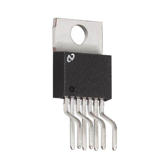
| 产品图片 |
|
| 产品型号 | LT3493EDCB#TRMPBF |
| PWM类型 | 电流模式 |
| rohs | 无铅 / 符合限制有害物质指令(RoHS)规范要求 |
| 产品系列 | - |
| 产品目录页面 | |
| 供应商器件封装 | 6-DFN(2x3) |
| 其它名称 | LT3493EDCB#TRMPBFCT |
| 包装 | 剪切带 (CT) |
| 同步整流器 | 无 |
| 安装类型 | 表面贴装 |
| 封装/外壳 | 6-WFDFN 裸露焊盘 |
| 工作温度 | -40°C ~ 85°C |
| 标准包装 | 1 |
| 电压-输入 | 3.6 V ~ 36 V |
| 电压-输出 | 0.78 V ~ 34.2 V |
| 电流-输出 | 1.2A |
| 类型 | 降压(降压) |
| 输出数 | 1 |
| 输出类型 | 可调式 |
| 频率-开关 | 750kHz |


- 商务部:美国ITC正式对集成电路等产品启动337调查
- 曝三星4nm工艺存在良率问题 高通将骁龙8 Gen1或转产台积电
- 太阳诱电将投资9.5亿元在常州建新厂生产MLCC 预计2023年完工
- 英特尔发布欧洲新工厂建设计划 深化IDM 2.0 战略
- 台积电先进制程称霸业界 有大客户加持明年业绩稳了
- 达到5530亿美元!SIA预计今年全球半导体销售额将创下新高
- 英特尔拟将自动驾驶子公司Mobileye上市 估值或超500亿美元
- 三星加码芯片和SET,合并消费电子和移动部门,撤换高东真等 CEO
- 三星电子宣布重大人事变动 还合并消费电子和移动部门
- 海关总署:前11个月进口集成电路产品价值2.52万亿元 增长14.8%


PDF Datasheet 数据手册内容提取
LT3493 1.2A, 750kHz Step-Down Switching Regulator in 2mm × 3mm DFN FEATURES DESCRIPTION n Wide Input Range: 3.6V to 36V Operating, The LT®3493 is a current mode PWM step-down DC/DC 40V Maximum converter with an internal 1.75A power switch. The wide n 1.2A Output Current operating input range of 3.6V to 36V (40V maximum) n Fixed Frequency Operation: 750kHz makes the LT3493 ideal for regulating power from a wide n Output Adjustable Down to 780mV variety of sources, including unregulated wall transform- n Short-Circuit Robust ers, 24V industrial supplies and automotive batteries. n Uses Tiny Capacitors and Inductors Its high operating frequency allows the use of tiny, low n Soft-Start cost inductors and ceramic capacitors, resulting in low, n Internally Compensated predictable output ripple. n Low Shutdown Current: <2μA Cycle-by-cycle current limit provides protection against n Low V Switch: 330mV at 1A CESAT shorted outputs and soft-start eliminates input current n Thermally Enhanced, Low Profi le DFN Package surge during start-up. The low current (<2μA) shutdown APPLICATIONS mode provides output disconnect, enabling easy power management in battery-powered systems. n Automotive Battery Regulation L, LT, LTC and LTM are registered trademarks of Linear Technology Corporation. n Industrial Control Supplies All other trademarks are the property of their respective owners. n Wall Transformer Regulation n Distributed Supply Regulation n Battery-Powered Equipment TYPICAL APPLICATION Effi ciency 3.3V Step-Down Converter 90 85 4.2V TO 3V6IVN VIN BOOST V3.O3UVT 80 ON OFF SHDNLT3493 SW 0.1μF 10μH 10..29A5A, V, VININ > >1 25VV CY (%) 75 32.4k 22pF CIEN 70 GND FB 10μF EFFI 65 1μF 10k 60 VIN = 12V 55 VOUT = 3.3V 3493 TA01a L = 10μH 50 0 0.2 0.4 0.6 0.8 1.0 1.2 LOAD CURRENT (A) 3493 TA01b 3493fb 1
LT3493 ABSOLUTE MAXIMUM RATINGS PIN CONFIGURATION (Note 1) Input Voltage (VIN) ....................................................40V TOP VIEW BOOST Pin Voltage ..................................................50V FB 1 6 SHDN BOOST Pin Above SW Pin .........................................25V SHDN Pin ..................................................................40V GND 2 7 5 VIN FB Voltage ...................................................................6V BOOST 3 4 SW Operating Temperature Range (Note 2) DCB PACKAGE LT3493E ..............................................–40°C to 85°C 6-LEAD (2mm (cid:115) 3mm) PLASTIC DFN LT3493I .............................................–40°C to 125°C TJMAX = 125°C, θJA = 64°C/W EXPOSED PAD (PIN 7) IS GND, MUST BE SOLDERED TO PCB Maximum Junction Temperature ..........................125°C Storage Temperature Range ...................–65°C to 150°C ORDER INFORMATION LEAD FREE FINISH TAPE AND REEL PART MARKING PACKAGE DESCRIPTION TEMPERATURE RANGE LT3493EDCB#PBF LT3493EDCB#TRPBF LCGG 6-Lead (2mm × 3mm) Plastic DFN –40°C to 85°C LT3493IDCB#PBF LT3493IDCB#TRPBF LCGH 6-Lead (2mm × 3mm) Plastic DFN –40°C to 125°C LEAD BASED FINISH TAPE AND REEL PART MARKING PACKAGE DESCRIPTION TEMPERATURE RANGE LT3493EDCB LT3493EDCB#TR LCGG 6-Lead (2mm × 3mm) Plastic DFN –40°C to 85°C LT3493IDCB LT3493IDCB#TR LCGH 6-Lead (2mm × 3mm) Plastic DFN –40°C to 125°C Consult LTC Marketing for parts specifi ed with wider operating temperature ranges. For more information on lead free part marking, go to: http://www.linear.com/leadfree/ For more information on tape and reel specifi cations, go to: http://www.linear.com/tapeandreel/ ELECTRICAL CHARACTERISTICS The l denotes the specifi cations which apply over the full operating temperature range, otherwise specifi cations are at T = 25°C. V = 12V, V = 17V, unless otherwise noted. (Note 2) A IN BOOST PARAMETER CONDITIONS MIN TYP MAX UNITS V Operating Range 3.6 36 V IN Undervoltage Lockout 3.1 3.4 3.6 V Feedback Voltage l 765 780 795 mV FB Pin Bias Current V = Measured V + 10mV (Note 4) l 50 150 nA FB REF Quiescent Current Not Switching 1.9 2.5 mA Quiescent Current in Shutdown V = 0V 0.01 2 μA SHDN Reference Line Regulation V = 5V to 36V 0.007 %/V IN Switching Frequency V = 0.7V 685 750 815 kHz FB V = 0V 36 kHz FB Maximum Duty Cycle l 88 95 % T = 25°C 91 95 % A 3493fb 2
LT3493 ELECTRICAL CHARACTERISTICS The l denotes the specifi cations which apply over the full operating temperature range, otherwise specifi cations are at T = 25°C. V = 12V, V = 17V, unless otherwise noted. (Note 2) A IN BOOST PARAMETER CONDITIONS MIN TYP MAX UNITS Switch Current Limit (Note 3) 1.4 1.75 2.2 A Switch V I = 1A 330 mV CESAT SW Switch Leakage Current 2 μA Minimum Boost Voltage Above Switch I = 1A 1.85 2.2 V SW BOOST Pin Current I = 1A 30 50 mA SW SHDN Input Voltage High 2.3 V SHDN Input Voltage Low 0.3 V SHDN Bias Current V = 2.3V (Note 5) 6 15 μA SHDN V = 0V 0.01 0.1 μA SHDN Note 1: Stresses beyond those listed under Absolute Maximum Ratings Note 3: Current limit guaranteed by design and/or correlation to static test. may cause permanent damage to the device. Exposure to any Absolute Slope compensation reduces current limit at higher duty cycle. Maximum Rating condition for extended periods may affect device Note 4: Current fl ows out of pin. reliability and lifetime. Note 5: Current fl ows into pin. Note 2: The LT3493E is guaranteed to meet performance specifi cations from 0°C to 85°C. Specifi cations over the –40°C to 85°C operating temperature range are assured by design, characterization and correlation with statistical process controls. The LT3493I specifi cations are guaranteed over the –40°C to 125°C temperature range. TYPICAL PERFORMANCE CHARACTERISTICS T = 25°C unless otherwise noted. A Effi ciency (V = 5V, L = 10μH) Effi ciency (V = 3.3V, L = 10μH) Effi ciency (V = 1.8V, L = 4.7μH) OUT OUT OUT 95 90 80 90 85 75 85 80 %) 80 %) 75 %) 70 Y ( 75 Y ( Y ( NC NC 70 NC 65 CIE 70 CIE CIE EFFI 65 EFFI 65 EFFI 60 60 60 VIN = 8V VIN = 8V 55 55 VIN = 12V 55 VIN = 12V VIN = 5V VIN = 24V VIN = 24V VIN = 12V 50 50 50 0 0.2 0.4 0.6 0.8 1.0 1.2 0 0.2 0.4 0.6 0.8 1.0 1.2 0 0.2 0.4 0.6 0.8 1.0 1.2 LOAD CURRENT (A) LOAD CURRENT (A) LOAD CURRENT (A) 3493 G01 3493 G02 3493 G03 3493fb 3
LT3493 TYPICAL PERFORMANCE CHARACTERISTICS T = 25°C unless otherwise noted. A Maximum Load Current, Maximum Load Current, Maximum Load Current, V = 5V, L = 8.2μH V = 5V, L = 33μH V = 3.3V, L = 4.7μH OUT OUT OUT 1.60 1.60 1.60 1.50 1.50 1.50 TYPICAL TYPICAL TYPICAL A)1.40 A)1.40 A)1.40 T ( T ( T ( N N N RE1.30 RE1.30 RE1.30 R R R U U U C C MINIMUM C T 1.20 T 1.20 T 1.20 U U U TP MINIMUM TP TP MINIMUM OU1.10 OU1.10 OU1.10 1.00 1.00 1.00 0.90 0.90 0.90 8 12 16 20 24 28 8 12 16 20 24 28 5 10 15 20 25 30 VIN (V) VIN (V) VIN (V) 3493 G04 3493 G22 3493 G05 Maximum Load Current, V = 3.3V, L = 10μH Switch Voltage Drop Undervoltage Lockout OUT 1.60 550 4.00 500 3.90 1.50 450 TYPICAL TA = 85°C 3.80 PUT CURRENT (A)111...324000 MINIMUM V (mV)CE(SW)223435050000000 TA = 25°C TA = –40°C UVLO (V)3333....64570000 T OU1.10 150 3.30 100 3.20 1.00 50 3.10 0.90 0 3.00 5 10 15 20 25 30 0 0.2 0.4 0.6 0.8 1.0 1.2 1.4 1.6 1.8 –50 –25 0 25 50 75 100 125 150 VIN (V) SWITCH CURRENT (A) TEMPERATURE (°C) 3493 G21 3493 G06 3493 G08 Switching Frequency Frequency Foldback Soft-Start 800 800 2.0 780 1.8 700 760 Hz) A) 1.6 FREQUENCY (kHz) 767762804600000 WITCHING FREQUENCY (k 462350000000000 WITCH CURRENT LIMIT ( 00111.....68042 640 S S 0.4 620 100 0.2 600 0 0 –50 –25 0 25 50 75 100 125 150 0 100 200 300 400 500 600 700 800 0 0.25 0.50 0.75 1 1.25 1.50 1.75 2 TEMPERATURE (°C) FEEDBACK VOLTAGE (mV) SHDN PIN VOLTAGE (V) 3493 G09 3493 G11 3493 G13 3493fb 4
LT3493 TYPICAL PERFORMANCE CHARACTERISTICS T = 25°C unless otherwise noted. A Typical Minimum Input Voltage Typical Minimum Input Voltage SHDN Pin Current (V = 5V) (V = 3.3V) OUT OUT 50 7.5 5.5 45 TO START 5.3 40 7.0 5.1 35 4.9 TO START A) 30 6.5 4.7 (μHDN 25 V (V)IN V (V)IN 4.5 IS 20 6.0 4.3 TO RUN 15 4.1 TO RUN 10 5.5 3.9 5 3.7 0 5.0 3.5 0 2 4 6 8 10 12 14 16 18 20 1 10 100 1000 1 10 100 1000 VSHDN (V) IOUT (mA) IOUT (mA) 3493 G14 3493 G15 3493 G16 Switch Current Limit Switch Current Limit 2.0 2.0 1.9 1.8 A) 1.8 A) 1.6 MIT ( 1.7 MIT ( 1.4 NT LI 1.6 NT LI 1.2 RE 1.5 RE 1.0 R R CU 1.4 CU 0.8 H H WITC 1.3 WITC 0.6 S 1.2 S 0.4 1.1 0.2 1.0 0 –50 –25 0 25 50 75 100 125 150 0 20 40 60 80 100 TEMPERATURE (°C) DUTY CYCLE (%) 3493 G17 3493 G18 Operating Waveforms, Operating Waveforms Discontinuous Mode VSW VSW 5V/DIV 5V/DIV 0.5A/DIIVL IL 0.5A/DIV 0 0 VOUT VOUT 20mV/DIV 20mV/DIV VIN = 12V 1μs/DIV 3493 G19 VIN = 12V 1μs/DIV 3493 G20 VOUT = 3.3V VOUT = 3.3V IOUT = 0.5A IOUT = 50mA L = 10μH L = 10μH COUT = 10μF COUT = 10μF 3493fb 5
LT3493 PIN FUNCTIONS FB (Pin 1): The LT3493 regulates its feedback pin to V (Pin 5): The V pin supplies current to the LT3493’s IN IN 780mV. Connect the feedback resistor divider tap to this internal regulator and to the internal power switch. This pin. Set the output voltage according to V = 0.78V • pin must be locally bypassed. OUT (1 + R1/R2). A good value for R2 is 10k. SHDN (Pin 6): The SHDN pin is used to put the LT3493 in GND (Pin 2): Tie the GND pin to a local ground plane shutdown mode. Tie to ground to shut down the LT3493. below the LT3493 and the circuit components. Return the Tie to 2.3V or more for normal operation. If the shutdown feedback divider to this pin. feature is not used, tie this pin to the V pin. SHDN also IN provides a soft-start function; see the Applications Infor- BOOST (Pin 3): The BOOST pin is used to provide a drive mation section. voltage, higher than the input voltage, to the internal bipolar NPN power switch. Exposed Pad (Pin 7): The Exposed Pad must be soldered to the PCB and electrically connected to ground. Use a SW (Pin 4): The SW pin is the output of the internal power large ground plane and thermal vias to optimize thermal switch. Connect this pin to the inductor, catch diode and performance. boost capacitor. BLOCK DIAGRAM VIN VIN 5 C2 INT REG AND UVLO D2 (cid:51) BOOST ON OFF 3 SLOPE R3 COMP R Q SHDN C3 6 S Q DRIVER Q1 C4 L1 OSC SW 4 VOUT D1 C1 FREQUENCY FOLDBACK VC gm 780mV GND FB 2 1 R2 R1 3493 BD 3493fb 6
LT3493 OPERATION (Refer to Block Diagram) The LT3493 is a constant frequency, current mode step- An internal regulator provides power to the control circuitry. down regulator. A 750kHz oscillator enables an RS fl ip-fl op, This regulator includes an undervoltage lockout to prevent turning on the internal 1.75A power switch Q1. An amplifi er switching when V is less than ~3.4V. The SHDN pin is IN and comparator monitor the current fl owing between the used to place the LT3493 in shutdown, disconnecting the V and SW pins, turning the switch off when this current output and reducing the input current to less than 2μA. IN reaches a level determined by the voltage at V . An error C The switch driver operates from either the input or from amplifi er measures the output voltage through an external the BOOST pin. An external capacitor and diode are used resistor divider tied to the FB pin and servos the V node. C to generate a voltage at the BOOST pin that is higher than If the error amplifi er’s output increases, more current is the input supply. This allows the driver to fully saturate the delivered to the output; if it decreases, less current is internal bipolar NPN power switch for effi cient operation. delivered. An active clamp (not shown) on the V node C provides current limit. The V node is also clamped to The oscillator reduces the LT3493’s operating frequency C the voltage on the SHDN pin; soft-start is implemented when the voltage at the FB pin is low. This frequency by generating a voltage ramp at the SHDN pin using an foldback helps to control the output current during start- external resistor and capacitor. up and overload. 3493fb 7
LT3493 APPLICATIONS INFORMATION FB Resistor Network of the V and BOOST pins. The input voltage should be IN limited to the V operating range (36V) during overload The output voltage is programmed with a resistor divider IN conditions (short-circuit or start-up). between the output and the FB pin. Choose the 1% resis- tors according to: Minimum On Time (cid:1) V (cid:3) R1 R2 OUT –1 The part will still regulate the output at input voltages that = (cid:5) (cid:6) 0.78V (cid:2) (cid:4) exceed V (up to 40V), however, the output voltage IN(MAX) R2 should be 20k or less to avoid bias current errors. ripple increases as the input voltage is increased. Figure 1 Reference designators refer to the Block Diagram. illustrates switching waveforms in continuous mode for a 3V output application near V = 33V. An optional phase lead capacitor of 22pF between V IN(MAX) OUT and FB reduces light-load output ripple. As the input voltage is increased, the part is required to switch for shorter periods of time. Delays associated Input Voltage Range with turning off the power switch dictate the minimum on time of the part. The minimum on time for the LT3493 The input voltage range for LT3493 applications depends on the output voltage and on the absolute maximum rat- is ~120ns. Figure 2 illustrates the switching waveforms ings of the VIN and BOOST pins. when the input voltage is increased to VIN = 35V. The minimum input voltage is determined by either the LT3493’s minimum operating voltage of 3.6V, or by its maximum duty cycle. The duty cycle is the fraction of VSW 20V/DIV time that the internal switch is on and is determined by the input and output voltages: IL V +V 0.5A/DIV OUT D DC= V –V +V IN SW D VOUT 200mV/DIV where VD is the forward voltage drop of the catch diode AC COUPLED (~0.4V) and VSW is the voltage drop of the internal switch COUT = 10μF 2μs/DIV 3493 F01 (~0.4V at maximum load). This leads to a minimum input VOUT = 3V VIN = 30V voltage of: ILOAD = 0.75A L = 10μH V V Figure 1 OUT + D V –V V IN(MIN) = DC D+ SW MAX with DCMAX = 0.91 (0.88 over temperature). VSW 20V/DIV The maximum input voltage is determined by the absolute maximum ratings of the V and BOOST pins. For con- IN IL tinuous mode operation, the maximum input voltage is 0.5A/DIV determined by the minimum duty cycle DC = 0.10: MIN V V VOUT OUT + D 200mV/DIV V –V V IN(MAX) = DC D+ SW AC COUPLED MIN COUT = 10μF 2μs/DIV 3493 F02 VOUT = 3V Note that this is a restriction on the operating input voltage VIN = 35V for continuous mode operation; the circuit will tolerate ILOAD = 0.75A L = 10μH transient inputs up to the absolute maximum ratings Figure 2 3493fb 8
LT3493 APPLICATIONS INFORMATION Now the required on-time has decreased below the Inductor Selection and Maximum Output Current minimum on time of 120ns. Instead of the switch pulse A good fi rst choice for the inductor value is: width becoming narrower to accommodate the lower duty cycle requirement, the switch pulse width remains fi xed L = 1.6 (VOUT + VD) at 120ns. In Figure 2 the inductor current ramps up to a where V is the voltage drop of the catch diode (~0.4V) and D value exceeding the load current and the output ripple L is in μH. With this value there will be no subharmonic increases to ~200mV. The part then remains off until the oscillation for applications with 50% or greater duty cycle. output voltage dips below 100% of the programmed value The inductor’s RMS current rating must be greater than before it begins switching again. your maximum load current and its saturation current Provided that the load can tolerate the increased output should be about 30% higher. For robust operation in fault voltage ripple and that the components have been properly conditions, the saturation current should be above 2.2A. selected, operation above V is safe and will not To keep effi ciency high, the series resistance (DCR) should IN(MAX) damage the part. Figure 3 illustrates the switching wave- be less than 0.1Ω. Table 1 lists several vendors and types forms when the input voltage is increased to its absolute that are suitable. maximum rating of 40V. Of course, such a simple design guide will not always As the input voltage increases, the inductor current ramps result in the optimum inductor for your application. A up quicker, the number of skipped pulses increases and larger value provides a higher maximum load current and the output voltage ripple increases. For operation above reduces output voltage ripple at the expense of slower V the only component requirement is that the com- transient response. If your load is lower than 1.2A, then IN(MAX) ponents be adequately rated for operation at the intended you can decrease the value of the inductor and operate voltage levels. with higher ripple current. This allows you to use a physi- cally smaller inductor, or one with a lower DCR resulting in The part is robust enough to survive prolonged operation higher effi ciency. There are several graphs in the Typical under these conditions as long as the peak inductor current Performance Characteristics section of this data sheet that does not exceed 2.2A. Inductor current saturation may show the maximum load current as a function of input further limit performance in this operating regime. voltage and inductor value for several popular output volt- ages. Low inductance may result in discontinuous mode operation, which is okay, but further reduces maximum VSW 20V/DIV load current. For details of the maximum output current and discontinuous mode operation, see Linear Technology Application Note 44. IL 0.5A/DIV Catch Diode VOUT Depending on load current, a 1A to 2A Schottky diode is 200mV/DIV AC COUPLED recommended for the catch diode, D1. The diode must COUT = 10μF 2μs/DIV 3493 F03 have a reverse voltage rating equal to or greater than the VOUT = 3V maximum input voltage. The ON Semiconductor MBRM140 VIN = 40V ILOAD = 0.75A is a good choice; it is rated for 1A continuous forward L = 10μH Figure 3 current and a maximum reverse voltage of 40V. 3493fb 9
LT3493 APPLICATIONS INFORMATION Table 1. Inductor Values VENDOR URL PART SERIES INDUCTANCE RANGE (μH) SIZE (MM) Sumida www.sumida.com CDRH4D28 1.2 to 4.7 4.5 × 4.5 CDRH5D28 2.5 to 10 5.5 × 5.5 CDRH8D28 2.5 to 33 8.3 × 8.3 Toko www.toko.com A916CY 2 to 12 6.3 × 6.2 D585LC 1.1 to 39 8.1 × 8.0 Würth Elektronik www.we-online.com WE-TPC(M) 1 to 10 4.8 × 4.8 WE-PD2(M) 2.2 to 22 5.2 × 5.8 WE-PD(S) 1 to 27 7.3 × 7.3 Input Capacitor determines the output ripple so low impedance at the switching frequency is important. The second function Bypass the input of the LT3493 circuit with a 1μF or is to store energy in order to satisfy transient loads and higher value ceramic capacitor of X7R or X5R type. Y5V stabilize the LT3493’s control loop. types have poor performance over temperature and ap- plied voltage and should not be used. A 1μF ceramic is Ceramic capacitors have very low equivalent series re- adequate to bypass the LT3493 and will easily handle the sistance (ESR) and provide the best ripple performance. ripple current. However, if the input power source has A good value is: high impedance, or there is signifi cant inductance due to C = 65/V OUT OUT long wires or cables, additional bulk capacitance may be necessary. This can be provided with a low performance where COUT is in μF. Use X5R or X7R types and keep in electrolytic capacitor. mind that a ceramic capacitor biased with VOUT will have less than its nominal capacitance. This choice will provide Step-down regulators draw current from the input sup- low output ripple and good transient response. Transient ply in pulses with very fast rise and fall times. The input performance can be improved with a high value capacitor, capacitor is required to reduce the resulting voltage but a phase lead capacitor across the feedback resistor ripple at the LT3493 and to force this very high frequency R1 may be required to get the full benefi t (see the Com- switching current into a tight local loop, minimizing EMI. pensation section). A 1μF capacitor is capable of this task, but only if it is placed close to the LT3493 and the catch diode; see the For small size, the output capacitor can be chosen ac- PCB Layout section. A second precaution regarding the cording to: ceramic input capacitor concerns the maximum input C = 25/V OUT OUT voltage rating of the LT3493. A ceramic input capacitor where C is in μF. However, using an output capacitor combined with trace or cable inductance forms a high OUT this small results in an increased loop crossover frequency quality (underdamped) tank circuit. If the LT3493 circuit and increased sensitivity to noise. A 22pF capacitor con- is plugged into a live supply, the input voltage can ring to nected between V and the FB pin is required to fi lter twice its nominal value, possibly exceeding the LT3493’s OUT noise at the FB pin and ensure stability. voltage rating. This situation is easily avoided; see the Hot Plugging Safely section. High performance electrolytic capacitors can be used for the output capacitor. Low ESR is important, so choose one Output Capacitor that is intended for use in switching regulators. The ESR The output capacitor has two essential functions. Along should be specifi ed by the supplier and should be 0.1Ω with the inductor, it fi lters the square wave generated or less. Such a capacitor will be larger than a ceramic by the LT3493 to produce the DC output. In this role it capacitor and will have a larger capacitance, because the 3493fb 10
LT3493 APPLICATIONS INFORMATION Table 2. Capacitor Vendors VENDOR PHONE URL PART SERIES COMMENTS Panasonic (714) 373-7366 www.panasonic.com Ceramic, Polymer, EEF Series Tantalum Kemet (864) 963-6300 www.kemet.com Ceramic, Tantalum T494, T495 Sanyo (408) 749-9714 www.sanyovideo.com Ceramic, Polymer, POSCAP Tantalum Murata (404) 436-1300 www.murata.com Ceramic AVX www.avxcorp.com Ceramic, Tantalum TPS Series Taiyo Yuden (864) 963-6300 www.taiyo-yuden.com Ceramic capacitor must be large to achieve low ESR. Table 2 lists effi cient because the BOOST pin current comes from a lower several capacitor vendors. voltage source. You must also be sure that the maximum voltage rating of the BOOST pin is not exceeded. Figure 4 shows the transient response of the LT3493 with several output capacitor choices. The output is 3.3V. The The minimum operating voltage of an LT3493 applica- load current is stepped from 250mA to 1A and back to tion is limited by the undervoltage lockout (3.6V) and by 250mA, and the oscilloscope traces show the output volt- the maximum duty cycle as outlined above. For proper age. The upper photo shows the recommended value. The start-up, the minimum input voltage is also limited by second photo shows the improved response (less voltage the boost circuit. If the input voltage is ramped slowly, drop) resulting from a larger output capacitor and a phase or the LT3493 is turned on with its SHDN pin when the lead capacitor. The last photo shows the response to a high output is already in regulation, then the boost capacitor performance electrolytic capacitor. Transient performance may not be fully charged. Because the boost capacitor is is improved due to the large output capacitance. charged with the energy stored in the inductor, the circuit will rely on some minimum load current to get the boost BOOST Pin Considerations circuit running properly. This minimum load will depend on the input and output voltages, and on the arrangement Capacitor C3 and diode D2 are used to generate a boost of the boost circuit. The minimum load generally goes to voltage that is higher than the input voltage. In most cases zero once the circuit has started. Figure 6 shows a plot of a 0.1μF capacitor and fast switching diode (such as the minimum load to start and to run as a function of input 1N4148 or 1N914) will work well. Figure 5 shows two voltage. In many cases the discharged output capacitor ways to arrange the boost circuit. The BOOST pin must will present a load to the switcher which will allow it to be at least 2.3V above the SW pin for best effi ciency. For start. The plots show the worst-case situation where V outputs of 3.3V and above, the standard circuit (Figure 5a) IN is ramping verly slowly. For lower start-up voltage, the is best. For outputs between 3V and 3.3V, use a 0.22μF boost diode can be tied to V ; however this restricts the capacitor. For outputs between 2.5V and 3V, use a 0.47μF IN input range to one-half of the absolute maximum rating capacitor and a small Schottky diode (such as the BAT- of the BOOST pin. 54). For lower output voltages the boost diode can be tied to the input (Figure 5b). The circuit in Figure 5a is more 3493fb 11
LT3493 APPLICATIONS INFORMATION ILOAD 2A/DIV VOUT IL 32.4k 0.5A/DIV FB 10μF 10k VOUT 0.1V/DIV AC COUPLED 40μs/DIV 3493 F04a ILOAD 2A/DIV VOUT 32.4k 3.3nF 0.5A/DIIVL 10μF FB (cid:115)2 10k VOUT 0.1V/DIV AC COUPLED 40μs/DIV 3493 F04b ILOAD VOUT 2A/DIV 32.4k + IL 0.5A/DIV FB 100μF 10k SANYO 4TPB100M VOUT 0.1V/DIV AC COUPLED 40μs/DIV 3493 F04c Figure 4. Transient Load Response of the LT3493 With Different Output Capacitors as the Load Current is Stepped from 250mA to 1A. V = 12V, V = 3.3V, L = 10μH IN OUT D2 D2 BOOST C3 BOOST C3 LT3493 LT3493 VIN VIN SW VOUT VIN VIN SW VOUT GND GND 3493 F05a 3493 F05b VBOOST – VSW(cid:32) VOUT VBOOST – VSW(cid:32) VIN MAX VBOOST(cid:32) VIN + VOUT MAX VBOOST(cid:32) 2VIN (5a) (5b) Figure 5. Two Circuits for Generating the Boost Voltage 3493fb 12
LT3493 APPLICATIONS INFORMATION 7.5 5.5 TO START 5.3 7.0 5.1 4.9 TO START 6.5 4.7 V) V) (N (N 4.5 VI VI 6.0 4.3 TO RUN 4.1 TO RUN 5.5 3.9 3.7 5.0 3.5 1 10 100 1000 1 10 100 1000 IOUT (mA) IOUT (mA) 3493 G15 3493 G16 (6a) Typical Minimum Input Voltage, V = 5V (6b) Typical Minimum Input Voltage, V = 3.3V OUT OUT Figure 6 At light loads, the inductor current becomes discontinu- where the output will be held high when the input to the ous and the effective duty cycle can be very high. This LT3493 is absent. This may occur in battery charging ap- reduces the minimum input voltage to approximately plications or in battery backup systems where a battery 400mV above V . At higher load currents, the inductor or some other supply is diode OR-ed with the LT3493’s OUT current is continuous and the duty cycle is limited by the output. If the V pin is allowed to fl oat and the SHDN pin IN maximum duty cycle of the LT3493, requiring a higher is held high (either by a logic signal or because it is tied input voltage to maintain regulation. to V ), then the LT3493’s internal circuitry will pull its IN quiescent current through its SW pin. This is fi ne if your Soft-Start system can tolerate a few mA in this state. If you ground the SHDN pin, the SW pin current will drop to essentially The SHDN pin can be used to soft-start the LT3493, reducing zero. However, if the V pin is grounded while the output the maximum input current during start-up. The SHDN pin IN is held high, then parasitic diodes inside the LT3493 can is driven through an external RC fi lter to create a voltage pull large currents from the output through the SW pin ramp at this pin. Figure 7 shows the start-up waveforms and the V pin. Figure 8 shows a circuit that will run only with and without the soft-start circuit. By choosing a large IN when the input voltage is present and that protects against RC time constant, the peak start-up current can be reduced a shorted or reversed input. to the current that is required to regulate the output, with no overshoot. Choose the value of the resistor so that it Hot Plugging Safely can supply 20μA when the SHDN pin reaches 2.3V. The small size, robustness and low impedance of ceramic Shorted and Reversed Input Protection capacitors make them an attractive option for the input bypass capacitor of LT3493 circuits. However, these capaci- If the inductor is chosen so that it won’t saturate exces- tors can cause problems if the LT3493 is plugged into a sively, an LT3493 buck regulator will tolerate a shorted live supply (see Linear Technology Application Note 88 for output. There is another situation to consider in systems 3493fb 13
LT3493 APPLICATIONS INFORMATION VSW 10V/DIV RUN SHDN IL 0.5A/DIV GND 3493 F07a VOUT 2V/DIV VIN = 12V 20μs/DIV VOUT = 3.3V L = 10μH COUT = 10μF VSW RUN 10V/DIV 15k SHDN IL 0.1μF GND 0.5A/DIV 3493 F07b VOUT 2V/DIV VIN = 12V 20μs/DIV VOUT = 3.3V L = 10μH COUT = 10μF Figure 7. To Soft-Start the LT3493, Add a Resistor and Capacitor to the SHDN Pin. V = 12V, V = 3.3V, C = 10μF, R = 5Ω IN OUT OUT LOAD D4 a complete discussion). The low loss ceramic capacitor VIN VIN BOOST combined with stray inductance in series with the power LT3493 source forms an underdamped tank circuit, and the voltage SHDN SW VOUT at the VIN pin of the LT3493 can ring to twice the nominal input voltage, possibly exceeding the LT3493’s rating and GND FB damaging the part. If the input supply is poorly controlled BACKUP or the user will be plugging the LT3493 into an energized supply, the input network should be designed to prevent D4: MBR0540 this overshoot. 3493 F08 Figure 8. Diode D4 Prevents a Shorted Input from Discharging Figure 9 shows the waveforms that result when an LT3493 a Backup Battery Tied to the Output; It Also Protects the Circuit circuit is connected to a 24V supply through six feet of from a Reversed Input. The LT3493 Runs Only When the Input 24-gauge twisted pair. The fi rst plot is the response with is Present 3493fb 14
LT3493 APPLICATIONS INFORMATION a 2.2μF ceramic capacitor at the input. The input voltage Frequency Compensation rings as high as 35V and the input current peaks at 20A. The LT3493 uses current mode control to regulate the One method of damping the tank circuit is to add another output. This simplifi es loop compensation. In particular, capacitor with a series resistor to the circuit. In Figure 9b the LT3493 does not require the ESR of the output capaci- an aluminum electrolytic capacitor has been added. This tor for stability allowing the use of ceramic capacitors to capacitor’s high equivalent series resistance damps the achieve low output ripple and small circuit size. circuit and eliminates the voltage overshoot. The extra capacitor improves low frequency ripple fi ltering and can Figure 10 shows an equivalent circuit for the LT3493 control slightly improve the effi ciency of the circuit, though it is loop. The error amp is a transconductance amplifi er with likely to be the largest component in the circuit. An alterna- fi nite output impedance. The power section, consisting of tive solution is shown in Figure 9c. A 1Ω resistor is added the modulator, power switch and inductor, is modeled as in series with the input to eliminate the voltage overshoot a transconductance amplifi er generating an output cur- (it also reduces the peak input current). A 0.1μF capacitor rent proportional to the voltage at the VC node. Note that improves high frequency fi ltering. This solution is smaller the output capacitor integrates this current, and that the and less expensive than the electrolytic capacitor. For high capacitor on the VC node (CC) integrates the error ampli- input voltages its impact on effi ciency is minor, reducing fi er output current, resulting in two poles in the loop. RC effi ciency less than one half percent for a 5V output at full provides a zero. With the recommended output capacitor, load operating from 24V. the loop crossover occurs above the RCCC zero. This simple CLOSING SWITCH SIMULATES HOT PLUG IIN VIN DANGER! LT3493 VIN + 20V/DIV RINGING VIN MAY EXCEED 2.2μF ABSOLUTE MAXIMUM RATING OF THE LT3493 IIN 5A/DIV LOW STRAY IMPEDANCE INDUCTANCE 20μs/DIV ENERGIZED DUE TO 6 FEET 24V SUPPLY (2 METERS) OF TWISTED PAIR (9a) LT3493 VIN + 10μF + 20V/DIV 35V 2.2μF AI.EI. IIN 5A/DIV (9b) 20μs/DIV 1Ω LT3493 VIN + 20V/DIV 0.1μF 2.2μF IIN 5A/DIV (9c) 20μs/DIV 3493 F09 Figure 9. A Well Chosen Input Network Prevents Input Voltage Overshoot and Ensures Reliable Operation When the LT3493 is Connected to a Live Supply 3493fb 15
LT3493 APPLICATIONS INFORMATION model works well as long as the value of the inductor is conditions, including load current, input voltage and tem- not too high and the loop crossover frequency is much perature. The LT1375 data sheet contains a more thorough lower than the switching frequency. With a larger ceramic discussion of loop compensation and describes how to capacitor (very low ESR), crossover may be lower and a test the stability using a transient load. phase lead capacitor (C ) across the feedback divider may PL improve the phase margin and transient response. Large PCB Layout electrolytic capacitors may have an ESR large enough to For proper operation and minimum EMI, care must be taken create an additional zero, and the phase lead may not be during printed circuit board layout. Figure 11 shows the necessary. recommended component placement with trace, ground If the output capacitor is different than the recommended plane and via locations. Note that large, switched currents capacitor, stability should be checked across all operating fl ow in the LT3493’s VIN and SW pins, the catch diode (D1) and the input capacitor (C2). The loop formed by these LT3493 CURRENT MODE components should be as small as possible and tied to 0.7V – POWER STAGE system ground in only one place. These components, along 1g.6mA =/V SW OUT with the inductor and output capacitor, should be placed on + R1 CPL the same side of the circuit board, and their connections – FB should be made on that layer. Place a local, unbroken ground VC gm = 300μA/V ESR plane below these components, and tie this ground plane 6R0Ck ERROR + 780mV + C1 to system ground at one location, ideally at the ground 100CpCF 1MAMPLIFIER C1 terminal of the output capacitor C1. The SW and BOOST nodes should be as small as possible. Finally, keep the R2 GND FB node small so that the ground pin and ground traces will shield it from the SW and BOOST nodes. Include vias 3493 F10 near the exposed GND pad of the LT3493 to help remove Figure 10. Model for Loop Response heat from the LT3493 to the ground plane. SYSTEM GROUND C2 D1 C1 VOUT VIN SHDN 3493 F11 : VIAS TO LOCAL GROUND PLANE : OUTLINE OF LOCAL GROUND PLANE Figure 11. A Good PCB Layout Ensures Proper, Low EMI Operation 3493fb 16
LT3493 APPLICATIONS INFORMATION High Temperature Considerations Outputs Greater Than 6V The die temperature of the LT3493 must be lower than the For outputs greater than 6V, add a resistor of 1k to 2.5k maximum rating of 125°C. This is generally not a concern across the inductor to damp the discontinuous ringing unless the ambient temperature is above 85°C. For higher of the SW node, preventing unintended SW current. The temperatures, care should be taken in the layout of the 12V Step-Down Converter circuit in the Typical Applica- circuit to ensure good heat sinking of the LT3493. The tions section shows the location of this resistor. Also note maximum load current should be derated as the ambient that for outputs above 6V, the input voltage range will be temperature approaches 125°C. The die temperature is limited by the maximum rating of the BOOST pin. The 12V calculated by multiplying the LT3493 power dissipation by circuit shows how to overcome this limitation using an the thermal resistance from junction to ambient. Power additional zener diode. dissipation within the LT3493 can be estimated by calcu- lating the total power loss from an effi ciency measure- Other Linear Technology Publications ment and subtracting the catch diode loss. The resulting Application notes AN19, AN35 and AN44 contain more temperature rise at full load is nearly independent of input detailed descriptions and design information for Buck voltage. Thermal resistance depends on the layout of the regulators and other switching regulators. The LT1376 circuit board, but 64°C/W is typical for the (2mm × 3mm) data sheet has a more extensive discussion of output DFN (DCB) package. ripple, loop compensation and stability testing. Design Note DN100 shows how to generate a bipolar output supply using a Buck regulator. TYPICAL APPLICATIONS 0.78V Step-Down Converter 1N4148 3.6V TO 2V5IVN VIN BOOST LT3493 0.1μF 3.3μH VOUT ON OFF SHDN SW 0.78V 1.2A MBRM140 GND FB 47μF 2.2μF 3493 TA02 1.8V Step-Down Converter 1N4148 3.6V TO 2V5IVN VIN BOOST LT3493 0.1μF 5μH VOUT ON OFF SHDN SW 1.8V 1.2A MBRM140 26.1k GND FB 22μF 2.2μF 20k 3493 TA03 3493fb 17
LT3493 TYPICAL APPLICATIONS 2.5V Step-Down Converter BAT54 3.6V TO 2V8IVN VIN BOOST V2.O5UVT LT3493 0.47μF6.8μH 11A.2,A V, IVNI N> 5>V 10V ON OFF SHDN SW MBRM140 22.1k GND FB 22μF 1μF 10k 3493 TA04 3.3V Step-Down Converter 4.2V TO 3V6IVN VIN BOOST 1N4148 V3.O3UVT LT3493 0.1μF 8.2μH 01..92AA,, VVIINN >> 41.25VV ON OFF SHDN SW MBRM140 32.4k GND FB 10μF 1μF 10k 3493 TA05 5V Step-Down Converter 6.4V TO 3V6IVN VIN BOOST 1N4148 V5VOUT LT3493 0.1μF 10μH 01..91AA,, VVIINN >> 71V4V ON OFF SHDN SW MBRM140 59k GND FB 10μF 1μF 11k 3493 TA06 3493fb 18
LT3493 PACKAGE DESCRIPTION DCB Package 6-Lead Plastic DFN (2mm × 3mm) (Reference LTC DWG # 05-08-1715) 0.70 ±0.05 1.65 ±0.05 3.55 ±0.05 (2 SIDES) 2.15 ±0.05 PACKAGE OUTLINE 0.25 ± 0.05 0.50 BSC 1.35 ±0.05 (2 SIDES) RECOMMENDED SOLDER PAD PITCH AND DIMENSIONS 2.00 ±0.10 R = 0.115 0.40 ± 0.10 (2 SIDES) TYP R = 0.05 4 6 TYP 3.00±0.10 1.65 ± 0.10 (2 SIDES) (2 SIDES) PIN 1 BAR PIN 1 NOTCH TOP MARK R0.20 OR 0.25 (SEE NOTE 6) (cid:115) 45° CHAMFER 3 1 (DCB6) DFN 0405 0.25 ± 0.05 0.200 REF 0.75 ±0.05 0.50 BSC 1.35 ±0.10 (2 SIDES) 0.00 – 0.05 BOTTOM VIEW—EXPOSED PAD NOTE: 1. DRAWING TO BE MADE A JEDEC PACKAGE OUTLINE M0-229 VARIATION OF (TBD) 2. DRAWING NOT TO SCALE 3. ALL DIMENSIONS ARE IN MILLIMETERS 4. DIMENSIONS OF EXPOSED PAD ON BOTTOM OF PACKAGE DO NOT INCLUDE MOLD FLASH. MOLD FLASH, IF PRESENT, SHALL NOT EXCEED 0.15mm ON ANY SIDE 5. EXPOSED PAD SHALL BE SOLDER PLATED 6. SHADED AREA IS ONLY A REFERENCE FOR PIN 1 LOCATION ON THE TOP AND BOTTOM OF PACKAGE 3493fb Information furnished by Linear Technology Corporation is believed to be accurate and reliable. 19 However, no responsibility is assumed for its use. Linear Technology Corporation makes no representa- tion that the interconnection of its circuits as described herein will not infringe on existing patent rights.
LT3493 TYPICAL APPLICATION 12V Step-Down Converter D1 6V 1N4148 1k* 0.25W 14.5V TO 3V6IVN VIN BOOST LT3493 0.1μF 22μH VOUT ON OFF SHDN SW 12V 1A MBRM140 71.5k GND FB 4.7μF 1μF 4.99k 3493 TA07 * FOR CONTINUOUS OPERATION ABOVE 30V USE TWO 2k, 0.25Ω RESISTORS IN PARALLEL. D1: CMDZ5235B RELATED PARTS PART NUMBER DESCRIPTION COMMENTS LT1766 60V, 1.2A I , 200kHz, High Effi ciency Step-Down V : 5.5V to 60V, V = 1.2V, I = 2.5mA, I = 25μA, OUT IN OUT(MIN) Q SD DC/DC Converter TSSOP16/TSSOP16E Packages LT1933 36V, 600mA I , 500kHz, High Effi ciency Step-Down OUT DC/DC Converter LT1936 36V, 1.4A I , 500kHz, High Effi ciency Step-Down OUT DC/DC Converter LT1940 25V, Dual 1.4A I , 1.1MHz, High Effi ciency Step-Down V : 3.6V to 25V, V = 1.25V, I = 3.8mA, I < 30μA, OUT IN OUT(MIN) Q SD DC/DC Converter TSSOP16E Package LT1976 60V, 1.2A I , 200kHz, High Effi ciency Step-Down V : 3.3V to 60V, V = 1.2V, I = 100μA, I < 1μA, OUT IN OUT(MIN) Q SD DC/DC Converter with Burst Mode® Operation TSSOP16E Package LT3010 80V, 50mA, Low Noise Linear Regulator V : 1.5V to 80V, V = 1.28V, I = 30μA, I < 1μA, IN OUT(MIN) Q SD MS8E Package LTC3407 Dual 600mA I , 1.5MHz, Synchronous Step-Down V : 2.5V to 5.5V, V = 0.6V, I = 40μA, I < 1μA, OUT IN OUT(MIN) Q SD DC/DC Converter MS10E Package LT3430/LT3431 60V, 2.75A I , 200kHz/500kHz, High Effi ciency Step-Down V : 5.5V to 60V, V = 1.2V, I = 2.5mA, I = 30μA, OUT IN OUT(MIN) Q SD DC/DC Converter TSSOP16E Package LT3470 40V, 200mA I , 26μA I , Step-Down DC/DC Converter OUT Q Burst Mode is a registered trademark of Linear Technology Corporation. 3493fb 20 Linear Technology Corporation LT 1108 REV B • PRINTED IN USA 1630 McCarthy Blvd., Milpitas, CA 95035-7417 (408) 432-1900 ● FAX: (408) 434-0507 ● www.linear.com © LINEAR TECHNOLOGY CORPORATION 2006