ICGOO在线商城 > 集成电路(IC) > PMIC - 稳压器 - DC DC 开关稳压器 > LT3480HMSE#PBF

 Datasheet下载
- 型号: LT3480HMSE#PBF
- 制造商: LINEAR TECHNOLOGY
- 库位|库存: xxxx|xxxx
- 要求:
| 数量阶梯 | 香港交货 | 国内含税 |
| +xxxx | $xxxx | ¥xxxx |
查看当月历史价格
查看今年历史价格
LT3480HMSE#PBF产品简介:
ICGOO电子元器件商城为您提供LT3480HMSE#PBF由LINEAR TECHNOLOGY设计生产,在icgoo商城现货销售,并且可以通过原厂、代理商等渠道进行代购。 LT3480HMSE#PBF价格参考。LINEAR TECHNOLOGYLT3480HMSE#PBF封装/规格:PMIC - 稳压器 - DC DC 开关稳压器, 可调式 降压 开关稳压器 IC 正 0.79V 1 输出 2A 10-TFSOP,10-MSOP(0.118",3.00mm 宽)裸露焊盘。您可以下载LT3480HMSE#PBF参考资料、Datasheet数据手册功能说明书,资料中有LT3480HMSE#PBF 详细功能的应用电路图电压和使用方法及教程。
| 参数 | 数值 |
| 产品目录 | 集成电路 (IC) |
| 描述 | IC REG BUCK ADJ 2A 10MSOP |
| 产品分类 | |
| 品牌 | Linear Technology |
| 数据手册 | http://www.linear.com/docs/19338 |
| 产品图片 |
|
| 产品型号 | LT3480HMSE#PBF |
| PWM类型 | 电流模式,Burst Mode® |
| rohs | 无铅 / 符合限制有害物质指令(RoHS)规范要求 |
| 产品系列 | - |
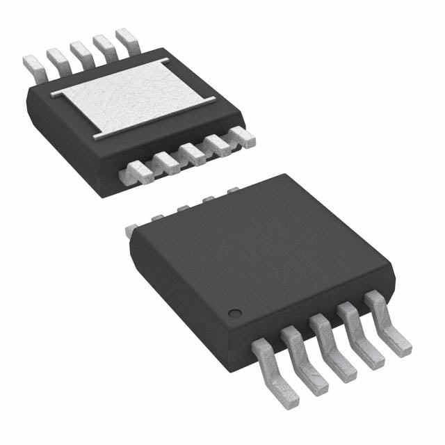
| 供应商器件封装 | 10-MSOP-EP |
| 其它名称 | LT3480HMSEPBF |
| 包装 | 管件 |
| 同步整流器 | 无 |
| 安装类型 | 表面贴装 |
| 封装/外壳 | 10-TFSOP,10-MSOP(0.118",3.00mm 宽)裸焊盘 |
| 工作温度 | -40°C ~ 150°C |
| 标准包装 | 50 |
| 电压-输入 | 3.6 V ~ 36 V |
| 电压-输出 | 0.79 V ~ 20 V |
| 电流-输出 | 2A |
| 类型 | 降压(降压) |
| 输出数 | 1 |
| 输出类型 | 可调式 |
| 频率-开关 | 200kHz ~ 2.4MHz |


- 商务部:美国ITC正式对集成电路等产品启动337调查
- 曝三星4nm工艺存在良率问题 高通将骁龙8 Gen1或转产台积电
- 太阳诱电将投资9.5亿元在常州建新厂生产MLCC 预计2023年完工
- 英特尔发布欧洲新工厂建设计划 深化IDM 2.0 战略
- 台积电先进制程称霸业界 有大客户加持明年业绩稳了
- 达到5530亿美元!SIA预计今年全球半导体销售额将创下新高
- 英特尔拟将自动驾驶子公司Mobileye上市 估值或超500亿美元
- 三星加码芯片和SET,合并消费电子和移动部门,撤换高东真等 CEO
- 三星电子宣布重大人事变动 还合并消费电子和移动部门
- 海关总署:前11个月进口集成电路产品价值2.52万亿元 增长14.8%


PDF Datasheet 数据手册内容提取
LT3480 36V, 2A, 2.4MHz Step-Down Switching Regulator with 70µA Quiescent Current FEATURES DESCRIPTION n Wide Input Range: The LT®3480 is an adjustable frequency (200kHz to Operation from 3.6V to 36V 2.4MHz) monolithic buck switching regulator that ac- Over-Voltage Lockout Protects Circuits cepts input voltages up to 36V (60V maximum). A high through 60V Transients efficiency 0.25 switch is included on the die along with n 2A Maximum Output Current a boost Schottky diode and the necessary oscillator, con- n Low Ripple Burst Mode® Operation trol, and logic circuitry. Current mode topology is used 70µA I at 12V to 3.3V for fast transient response and good loop stability. Low Q IN OUT Output Ripple < 15mV ripple Burst Mode operation maintains high efficiency at n Adjustable Switching Frequency: 200kHz to 2.4MHz low output currents while keeping output ripple below n Low Shutdown Current: I < 1µA 15mV in a typical application. In addition, the LT3480 can Q n Integrated Boost Diode further enhance low output current efficiency by draw- n Synchronizable Between 250kHz to 2MHz ing bias current from the output when V is above 3V. OUT n Power Good Flag Shutdown reduces input supply current to less than 1µA n Saturating Switch Design: 0.25 On-Resistance while a resistor and capacitor on the RUN/SS pin provide a n 0.790V Feedback Reference Voltage controlled output voltage ramp (soft-start). A power good n Output Voltage: 0.79V to 20V flag signals when V reaches 86% of the programmed OUT n Soft-Start Capability output voltage. The LT3480 is available in 10-lead MSOP n Small 10-Lead Thermally Enhanced MSOP and and 3mm × 3mm DFN packages with exposed pads for (3mm × 3mm) DFN Packages low thermal resistance. , LT, LTC and LTM are registered trademarks of Linear Technology Corporation. APPLICATIONS Burst Mode is a registered trademark of Linear Technology Corporation. All other trademarks are the property of their respective owners. n Automotive Battery Regulation n Power for Portable Products n Distributed Supply Regulation n Industrial Supplies TYPICAL APPLICATION 3.3V Step-Down Converter Efficiency VIN VOUT 100 4.5V TO 36V 3.3V TRANTSOI E6N0VT VIN BD 2A 90 VOUT = 5V OFF ON RUN/SS BOOST 14k 0.47µF 4.7µH Y (%) 80 VOUT = 3.3V 4.7µF 470pF VRCT LT3480 SW EFFICIENC 70 PG 316k 60 40.2k SYNC GND FB VL I=N 5=. 61µ2HV 100k 22µF 50 F = 800 kHz 0 0.5 1.0 1.5 2 LOAD CURRENT (A) 3480 TA01 3480 TA01b 3480fe 1 For more information www.linear.com/LT3480
LT3480 ABSOLUTE MAXIMUM RATINGS (Note 1) V , RUN/SS Voltage (Note 5) ...................................60V Storage Temperature Range ...................–65°C to 150°C IN BOOST Pin Voltage ...................................................56V Lead Temperature (Soldering, 10 sec) BOOST Pin Above SW Pin .........................................30V (MSE Only) .......................................................300°C FB, RT, V Voltage .......................................................5V C PG, BD, SYNC Voltage ..............................................30V Operating Junction Temperature Range (Note 2) LT3480E .............................................–40°C to 125°C LT3480I ..............................................–40°C to 125°C LT3480H ............................................–40°C to 150°C LT3480MP..........................................–55°C to 150°C PIN CONFIGURATION TOP VIEW TOP VIEW BD 1 10 RT BD 1 10 RT BOOST 2 9 VC BOOST 2 9 VC SW 3 11 8 FB SW 3 11 8 FB VIN 4 7 PG RUN/VSISN 45 76 PSGYNC RUN/SS 5 6 SYNC MSE PACKAGE 10-LEAD PLASTIC MSOP DD PACKAGE 10-LEAD (3mm × 3mm) PLASTIC DFN JA = 45°C/W, JC = 10°C/W EXPOSED PAD (PIN 11) IS GND, MUST BE SOLDERED TO PCB JA = 45°C/W, JC = 10°C/W EXPOSED PAD (PIN 11) IS GND, MUST BE SOLDERED TO PCB ORDER INFORMATION LEAD FREE FINISH TAPE AND REEL PART MARKING* PACKAGE DESCRIPTION TEMPERATURE RANGE LT3480EDD#PBF LT3480EDD#TRPBF LCTP 10-Lead (3mm × 3mm) Plastic DFN –40°C to 125°C LT3480IDD#PBF LT3480IDD#TRPBF LCTP 10-Lead (3mm × 3mm) Plastic DFN –40°C to 125°C LT3480EMSE#PBF LT3480EMSE#TRPBF LTCTM 10-Lead Plastic MSOP –40°C to 125°C LT3480IMSE#PBF LT3480IMSE#TRPBF LTCTM 10-Lead Plastic MSOP –40°C to 125°C LT3480HMSE#PBF LT3480HMSE#TRPBF LTCTM 10-Lead Plastic MSOP –40°C to 150°C LT3480MPMSE#PBF LT3480MPMSE#TRPBF LTCTM 10-Lead Plastic MSOP –55°C to 150°C LEAD BASED FINISH TAPE AND REEL PART MARKING* PACKAGE DESCRIPTION TEMPERATURE RANGE LT3480EDD LT3480EDD#TR LCTP 10-Lead (3mm × 3mm) Plastic DFN –40°C to 125°C LT3480IDD LT3480IDD#TR LCTP 10-Lead (3mm × 3mm) Plastic DFN –40°C to 125°C LT3480EMSE LT3480EMSE#TR LTCTM 10-Lead Plastic MSOP –40°C to 125°C LT3480IMSE LT3480IMSE#TR LTCTM 10-Lead Plastic MSOP –40°C to 125°C LT3480HMSE LT3480HMSE#TR LTCTM 10-Lead Plastic MSOP –40°C to 150°C LT3480MPMSE LT3480MPMSE#TR LTCTM 10-Lead Plastic MSOP –55°C to 150°C Consult LTC Marketing for parts specified with wider operating temperature ranges. *The temperature grade is identified by a label on the shipping container. For more information on lead free part marking, go to: http://www.linear.com/leadfree/ For more information on tape and reel specifications, go to: http://www.linear.com/tapeandreel/ 3480fe 2 For more information www.linear.com/LT3480
LT3480 ELECTRICAL CHARACTERISTICS The l denotes the specifications which apply over the full operating temperature range, otherwise specifications are at T = 25°C. V = 10V, V = 10V, V = 15V, V = 3.3V unless otherwise noted. (Note 2) A IN RUN/SS BOOST BD PARAMETER CONDITIONS MIN TYP MAX UNITS Minimum Input Voltage l 3 3.6 V V Overvoltage Lockout l 36 38 40 V IN Quiescent Current from V V = 0.2V 0.01 0.5 µA IN RUN/SS V = 3V, Not Switching l 30 100 µA BD V = 0, Not Switching 105 160 µA BD Quiescent Current from BD V = 0.2V 0.01 0.5 µA RUN/SS V = 3V, Not Switching l 80 120 µA BD V = 0, Not Switching 1 5 µA BD Minimum Bias Voltage (BD Pin) 2.7 3 V Feedback Voltage 780 790 800 mV l 775 790 805 mV FB Pin Bias Current (Note 3) V = 0.8V, V = 0.4V l 7 30 nA FB C FB Voltage Line Regulation 4V < V < 36V 0.002 0.01 %/V IN Error Amp g 400 µMho m Error Amp Gain 1000 V Source Current 45 µA C V Sink Current 45 µA C V Pin to Switch Current Gain 3.5 A/V C V Clamp Voltage 2 V C Switching Frequency R = 8.66k 2.1 2.4 2.7 MHz T R = 29.4k 0.9 1 1.15 MHz T R = 187k 160 200 240 kHz T Minimum Switch Off-Time l 60 150 nS Switch Current Limit Duty Cycle = 5% 3 3.5 4 A Switch V I = 2A 500 mV CESAT SW Boost Schottky Reverse Leakage V = 0V 0.02 2 µA BD Minimum Boost Voltage (Note 4) l 1.5 2.1 V BOOST Pin Current I = 1A 22 35 mA SW RUN/SS Pin Current V = 2.5V 5 10 µA RUN/SS RUN/SS Input Voltage High 2.5 V RUN/SS Input Voltage Low 0.2 V PG Threshold Offset from Feedback Voltage V Rising 100 mV FB PG Hysteresis 12 mV PG Leakage V = 5V 0.1 1 µA PG PG Sink Current V = 0.4V l 100 600 µA PG SYNC Low Threshold 0.5 V SYNC High Threshold 0.7 V SYNC Pin Bias Current V = 0V 0.1 µA SYNC Note 1: Stresses beyond those listed under Absolute Maximum Ratings Note 2: The LT3480E is guaranteed to meet performance specifications may cause permanent damage to the device. Exposure to any Absolute from 0°C to 125°C. Specifications over the –40°C to 125°C operating Maximum Rating condition for extended periods may affect device temperature range are assured by design, characterization and correlation reliability and lifetime. with statistical process controls. The LT3480I specifications are 3480fe 3 For more information www.linear.com/LT3480
LT3480 ELECTRICAL CHARACTERISTICS guaranteed over the –40°C to 125°C temperature range. The LT3480H Note 4: This is the minimum voltage across the boost capacitor needed to specifications are guaranteed over the –40°C to 150°C temperature range. guarantee full saturation of the switch. The LT3480MP specifications are guaranteed over the –55°C to 150°C Note 5: For operation at T ≤ 125°C, the absolute maximum voltage at V J IN temperature range. and RUN/SS pins is 40V for continuous operation and 60V for up to Note 3: Bias current flows out of the FB pin. 1 second nonrepetitive transients. For operation at TJ > 125°C, the absolute maximum voltage at V and RUN/SS pins is 36V. IN TYPICAL PERFORMANCE CHARACTERISTICS Efficiency Efficiency Efficiency 100 90 90 10 VIN = 7V VIN = 12V 85 VIN = 12V 80 90 80 ENCY (%) 80 VIN = 24V VIN = 34V ENCY (%) 7705 VIN = 24V VIN = 34V ENCY (%) 6700 1 POWER LO EFFICI 70 EFFICI 65 EFFICI 50 0.1 SS (W ) 60 60 VIN = 12V 40 VOUT = 3.3V 55 L = 5.6µH L: NEC PLC-0745-5R6 L: NEC PLC-0745-5R6 50 VOUT = 5V f: 800kHz 50 VOUT = 3.3V f: 800kHz 30 F = 800 kHz 0.01 0 0.2 0.4 0.6 0.8 1.0 1.2 1.4 1.6 1.8 2.0 0 0.2 0.4 0.6 0.8 1.0 1.2 1.4 1.6 1.8 2.0 0 0.5 1.0 1.5 2 LOAD CURRENT (A) LOAD CURRENT (A) LOAD CURRENT (A) 3480 G27 3480 G01 3480 G02 No Load Supply Current No Load Supply Current Maximum Load Current 120 400 4.0 VOUT = 3.3V CATCH DIODE: DIODES, INC. PDS360 350 100 VIN = 12V 3.5 PPLY CURRENT (µA) 486000 PPLY CURRENT (µA) 232100550000 VOUT = 3.3VICDHNUIICOGRRDHREE TEA LENSEMTEA PDDKE UASREGUA EPTT OPUAL TRCY EATCH OAD CURRENT (A) 232...500 TMYIPNIICMAULM U U L S S 100 VOUT = 3.3V 20 1.5 TA = 25 °C 50 L = 4.7µH f = 800 kHz 0 0 1.0 0 5 10 15 20 25 30 35 –50 –25 0 25 50 75 100 125 150 5 10 15 20 25 30 INPUT VOLTAGE (V) TEMPERATURE (°C) INPUT VOLTAGE (V) 3480 G04 3480 G05 3480 G06 3480fe 4 For more information www.linear.com/LT3480
LT3480 TYPICAL PERFORMANCE CHARACTERISTICS Maximum Load Current Switch Current Limit Switch Current Limit 3.5 4.0 4.5 TYPICAL 4.0 DUTY CYCLE = 10 % 3.5 3.0 A) A) 3.5 RRENT (A) 2.5 MINIMUM RENT LIMIT( 23..50 RENT LIMIT ( 23..50 DUTY CYCLE = 90 % LOAD CU 12..50 VTAO U=T 2 =5 5°VC SWITCH CUR 12..50 SWITCH CUR 112...500 L = 4.7µH 0.5 f = 800kHz 1.0 1.0 0 5 10 15 20 25 30 0 20 40 60 80 100 –50 –25 0 25 50 75 100 125 150 INPUT VOLTAGE (V) DUTY CYCLE (%) TEMPERATURE (°C) 3480 G07 3480 G08 3480 G09 Switch Voltage Drop Boost Pin Current Feedback Voltage 700 80 840 600 70 A) 60 V) 820 mV) 500 T (m E (m VOLTAGE DROP ( 432000000 OOST PIN CURREN 34520000 FEEDBACK VOLTAG 870800 B 100 10 0 0 760 0 500 1000 1500 2000 2500 0 500 1000 1500 2000 2500 –50 –25 0 25 50 75 100 125 150 SWITCH CURRENT (mA) SWITCH CURRENT (mA) TEMPERATURE (°C) 3480 G10 3480 G11 4380 G12 Switching Frequency Frequency Foldback Minimum Switch On-Time 1.20 1200 140 FREQUENCY (MHz) 110011......019901000555 WITCHING FREQUENCY (kHz)1046800000000 NIMUM SWITCH ON TIME (ns)118264000000 S 200 MI 0.85 20 0.80 0 0 –50 –25 0 25 50 75 100 125 150 0 100 200 300 400 500 600 700 800 900 –50 –25 0 25 50 75 100 125 150 TEMPERATURE (°C) FB PIN VOLTAGE (mV) TEMPERATURE (˚C) 4380 G13 3480 G14 3480 G15 3480fe 5 For more information www.linear.com/LT3480
LT3480 TYPICAL PERFORMANCE CHARACTERISTICS Soft-Start RUN/SS Pin Current Boost Diode 4.0 12 1.4 3.5 10 1.2 LIMIT (A) 32..05 ENT (µA) 8 V (V)f 1.0 WITCH CURRENT 121...005 UN/SS PIN CURR 46 BOOST DIODE 000...864 S R 2 0.5 0.2 0 0 0 0 0.5 1 1.5 2 2.5 3 3.5 0 5 10 15 20 25 30 35 0 0.5 1.0 1.5 2.0 RUN/SS PIN VOLTAGE (V) RUN/SS PIN VOLTAGE (V) BOOST DIODE CURRENT (A) 3480 G16 3480 G17 3480 G18 Error Amp Output Current Minimum Input Voltage Minimum Input Voltage 50 5.0 6.5 40 4.5 30 6.0 NT (µA) 2100 GE (V) 4.0 GE (V) 5.5 RRE 0 OLTA 3.5 OLTA U V V N C–10 UT UT 5.0 VPIC ––2300 INP 32..05 TVAO U=T 2 =5 °3C.3V INP 4.5 VTAO U=T 2 =5 5°VC –40 L = 4.7µH L = 4.7µH f = 800kHz f = 800kHz –50 2.0 4.0 –200 –100 0 100 200 1 10 100 1000 10000 1 10 100 1000 10000 FB PIN ERROR VOLTAGE (V) LOAD CURRENT (A) LOAD CURRENT (A) 3480 G19 3480 G20 3480 G21 V Voltages Power Good Threshold Switching Waveforms; Burst Mode C 2.50 95 2.00 CURRENT LIMIT CLAMP %) 90 5VV/DSIWV GE (V) 1.50 OLTAGE ( LTA D V 85 IL V VOC 1.00 SWITCHING THRESHOLD SHOL 0.2A/DIV E R H 80 0.50 T VOUT 10mV/DIV 0 75 –50 –25 0 25 50 75 100 125 150 –50 –25 0 25 50 75 100 125 150 5µs/DIV 3480 G24 TEMPERATURE (°C) TEMPERATURE (°C) VIN = 12V; FRONT PAGE APPLICATION 3480 G22 3480 G23 ILOAD = 10mA 3480fe 6 For more information www.linear.com/LT3480
LT3480 TYPICAL PERFORMANCE CHARACTERISTICS Switching Waveforms; Transition Switching Waveforms; Full from Burst Mode to Full Frequency Frequency Continuous Operation VSW VSW 5V/DIV 5V/DIV IL IL 0.2A/DIV 0.5A/DIV VOUT VOUT 10mV/DIV 10mV/DIV 1µs/DIV 3480 G25 1µs/DIV 3480 G26 VIN = 12V; FRONT PAGE APPLICATION VIN = 12V; FRONT PAGE APPLICATION ILOAD = 110mA ILOAD = 1A PIN FUNCTIONS BD (Pin 1): This pin connects to the anode of the boost SYNC (Pin 6): This is the external clock synchronization Schottky diode. BD also supplies current to the internal input. Ground this pin for low ripple Burst Mode operation at regulator. BD must be locally bypassed when not tied to low output loads. Tie to a clock source for synchronization. V with a low ESR capacitor (1µF). Clock edges should have rise and fall times faster than 1µs. OUT See synchronizing section in Applications Information. BOOST (Pin 2): This pin is used to provide a drive voltage, higher than the input voltage, to the internal bipolar PG (Pin 7): The PG pin is the open collector output of an NPN power switch. internal comparator. PG remains low until the FB pin is within 14% of the final regulation voltage. PG output is SW (Pin 3): The SW pin is the output of the internal power valid when V is above 3.6V and RUN/SS is high. switch. Connect this pin to the inductor, catch diode and IN boost capacitor. FB (Pin 8): The LT3480 regulates the FB pin to 0.790V. Connect the feedback resistor divider tap to this pin. V (Pin 4): The V pin supplies current to the LT3480’s IN IN internal regulator and to the internal power switch. This V (Pin 9): The V pin is the output of the internal error C C pin must be locally bypassed. amplifier. The voltage on this pin controls the peak switch current. Tie an RC network from this pin to ground to RUN/SS (Pin 5): The RUN/SS pin is used to put the compensate the control loop. LT3480 in shutdown mode. Tie to ground to shut down the LT3480. Tie to 2.5V or more for normal operation. If RT (Pin 10): Oscillator Resistor Input. Connecting a resistor the shutdown feature is not used, tie this pin to the V to ground from this pin sets the switching frequency. IN pin. RUN/SS also provides a soft-start function; see the Exposed Pad (Pin 11): Ground. The exposed pad must Applications Information section. be soldered to PCB. 3480fe 7 For more information www.linear.com/LT3480
LT3480 BLOCK DIAGRAM VIN 4 VIN C1 INTERNAL 0.79V REF – BD + 1 RUN/SS 5 Σ SLOPE COMP SWITCH BOOST LATCH 2 C3 R 10 RT 20O0SkCHIzL–L2A.T4OMRHz S Q L1 SW RT SYNC DISABLE 3 VOUT 6 C2 D1 Burst Mode SOFT-START DETECT PG 7 ERROR AMP VC CLAMP + 0.7V + VC 9 – – CC CF RC GND FB 11 8 R2 R1 3480 BD OPERATION The LT3480 is a constant frequency, current mode step- (typically the regulated output voltage). This improves down regulator. An oscillator, with frequency set by RT, efficiency. The RUN/SS pin is used to place the LT3480 enables an RS flip-flop, turning on the internal power in shutdown, disconnecting the output and reducing the switch. An amplifier and comparator monitor the current input current to less than 1µA. flowing between the V and SW pins, turning the switch IN The switch driver operates from either the input or from off when this current reaches a level determined by the the BOOST pin. An external capacitor and diode are used voltage at V . An error amplifier measures the output C to generate a voltage at the BOOST pin that is higher than voltage through an external resistor divider tied to the FB the input supply. This allows the driver to fully saturate the pin and servos the V pin. If the error amplifier’s output C internal bipolar NPN power switch for efficient operation. increases, more current is delivered to the output; if it decreases, less current is delivered. An active clamp on the To further optimize efficiency, the LT3480 automatically V pin provides current limit. The V pin is also clamped to switches to Burst Mode operation in light load situations. C C the voltage on the RUN/SS pin; soft-start is implemented Between bursts, all circuitry associated with controlling by generating a voltage ramp at the RUN/SS pin using an the output switch is shut down, reducing the input supply external resistor and capacitor. current to 70µA in a typical application. An internal regulator provides power to the control circuitry. The oscillator reduces the LT3480’s operating frequency when The bias regulator normally draws power from the V pin, the voltage at the FB pin is low. This frequency foldback helps IN but if the BD pin is connected to an external voltage higher to control the output current during startup and overload. than 3V bias power will be drawn from the external source 3480fe 8 For more information www.linear.com/LT3480
LT3480 OPERATION The LT3480 contains a power good comparator which trips The LT3480 has an overvoltage protection feature which when the FB pin is at 86% of its regulated value. The PG disables switching action when the V goes above 38V IN output is an open-collector transistor that is off when the typical (36V minimum). When switching is disabled, the output is in regulation, allowing an external resistor to pull LT3480 can safely sustain input voltages up to 60V. the PG pin high. Power good is valid when the LT3480 is enabled and V is above 3.6V. IN APPLICATIONS INFORMATION FB Resistor Network Operating Frequency Tradeoffs The output voltage is programmed with a resistor divider Selection of the operating frequency is a tradeoff between between the output and the FB pin. Choose the 1% resis- efficiency, component size, minimum dropout voltage, and tors according to: maximum input voltage. The advantage of high frequency operation is that smaller inductor and capacitor values may V R1=R2 OUT −1 be used. The disadvantages are lower efficiency, lower 0.79V maximum input voltage, and higher dropout voltage. The highest acceptable switching frequency (f ) for a SW(MAX) Reference designators refer to the Block Diagram. given application can be calculated as follows: Setting the Switching Frequency V +V f = D OUT The LT3480 uses a constant frequency PWM architecture SW(MAX) tON(MIN)(VD+VIN–VSW) that can be programmed to switch from 200kHz to 2.4MHz where V is the typical input voltage, V is the output by using a resistor tied from the RT pin to ground. A table IN OUT showing the necessary RT value for a desired switching voltage, VD is the catch diode drop (~0.5V) and VSW is the frequency is in Figure 1. internal switch drop (~0.5V at max load). This equation shows that slower switching frequency is necessary to SWITCHING FREQUENCY (MHz) RT VALUE (kΩ) safely accommodate high VIN/VOUT ratio. Also, as shown 0.2 187 in the next section, lower frequency allows a lower dropout 0.3 121 voltage. The reason input voltage range depends on the 0.4 88.7 0.5 68.1 switching frequency is because the LT3480 switch has finite 0.6 56.2 minimum on and off times. The switch can turn on for a 0.7 46.4 0.8 40.2 minimum of ~150ns and turn off for a minimum of ~150ns. 0.9 34 Typical minimum on time at 25°C is 80ns. This means that 1.0 29.4 the minimum and maximum duty cycles are: 1.2 23.7 1.4 19.1 DC =f t 1.6 16.2 MIN SW ON(MIN) 1.8 13.3 DC =1–f t 2.0 11.5 MAX SW OFF(MIN) 2.2 9.76 2.4 8.66 where f is the switching frequency, the t is the SW ON(MIN) minimum switch on time (~150ns), and the t is Figure 1. Switching Frequency vs. R Value OFF(MIN) T the minimum switch off time (~150ns). These equations show that duty cycle range increases when switching frequency is decreased. 3480fe 9 For more information www.linear.com/LT3480
LT3480 APPLICATIONS INFORMATION A good choice of switching frequency should allow ad- maximum duty cycle (see equation in previous section). equate input voltage range (see next section) and keep The minimum input voltage due to duty cycle is: the inductor and capacitor values small. V +V V = OUT D –V +V IN(MIN) D SW Input Voltage Range 1–f t SW OFF(MIN) The maximum input voltage for LT3480 applications depends where V is the minimum input voltage, and t on switching frequency, the Absolute Maximum Ratings of IN(MIN) OFF(MIN) is the minimum switch off time (150ns). Note that higher the V and BOOST pins, and the operating mode. IN switching frequency will increase the minimum input The LT3480 can operate from input voltages up to 38V, voltage. If a lower dropout voltage is desired, a lower and safely withstand input voltages up 60V. Note that while switching frequency should be used. V >38V (typical), the LT3480 will stop switching, allowing IN the output to fall out of regulation. Inductor Selection While the output is in start-up, short-circuit, or other For a given input and output voltage, the inductor value overload conditions, the switching frequency should be and switching frequency will determine the ripple current. chosen according to the following discussion. The ripple current ΔI increases with higher V or V L IN OUT and decreases with higher inductance and faster switching For safe operation at inputs up to 60V the switching fre- frequency. A reasonable starting point for selecting the quency must be set low enough to satisfy V ≥ 40V IN(MAX) ripple current is: according to the following equation. If lower V is IN(MAX) desired, this equation can be used directly. ΔI = 0.4(I ) L OUT(MAX) V = VOUT+VD –V +V where IOUT(MAX) is the maximum output load current. To IN(MAX) D SW guarantee sufficient output current, peak inductor current f t SW ON(MIN) must be lower than the LT3480’s switch current limit (I ). LIM where V is the maximum operating input voltage, The peak inductor current is: IN(MAX) V is the output voltage, V is the catch diode drop OUT D I = I + ΔI /2 L(PEAK) OUT(MAX) L (~0.5V), V is the internal switch drop (~0.5V at max SW where I is the peak inductor current, I is load), f is the switching frequency (set by R ), and L(PEAK) OUT(MAX) SW T the maximum output load current, and ΔI is the inductor t is the minimum switch on time (~150ns). Note that L ON(MIN) ripple current. The LT3480’s switch current limit (I ) is a higher switching frequency will depress the maximum LIM at least 3.5A at low duty cycles and decreases linearly to operating input voltage. Conversely, a lower switching 2.5A at DC = 0.8. The maximum output current is a func- frequency will be necessary to achieve safe operation at tion of the inductor ripple current: high input voltages. I = I – ΔI /2 If the output is in regulation and no short-circuit, start- OUT(MAX) LIM L up, or overload events are expected, then input voltage Be sure to pick an inductor ripple current that provides transients of up to 60V are acceptable regardless of the sufficient maximum output current (I ). OUT(MAX) switching frequency. In this mode, the LT3480 may enter The largest inductor ripple current occurs at the highest pulse skipping operation where some switching pulses V . To guarantee that the ripple current stays below the are skipped to maintain output regulation. In this mode IN specified maximum, the inductor value should be chosen the output voltage ripple and inductor current ripple will according to the following equation: be higher than in normal operation. Above 38V switching will stop. V +V V +V L= OUT D 1– OUT D The minimum input voltage is determined by either the fSW∆IL VIN(MAX) LT3480’s minimum operating voltage of ~3.6V or by its 3480fe 10 For more information www.linear.com/LT3480
LT3480 APPLICATIONS INFORMATION where V is the voltage drop of the catch diode (~0.4V), Input Capacitor D V is the maximum input voltage, V is the output IN(MAX) OUT Bypass the input of the LT3480 circuit with a ceramic capaci- voltage, f is the switching frequency (set by RT), and L SW tor of X7R or X5R type. Y5V types have poor performance is in the inductor value. over temperature and applied voltage, and should not be The inductor’s RMS current rating must be greater than the used. A 4.7µF to 10µF ceramic capacitor is adequate to maximum load current and its saturation current should be bypass the LT3480 and will easily handle the ripple current. about 30% higher. For robust operation in fault conditions Note that larger input capacitance is required when a lower (start-up or short circuit) and high input voltage (>30V), switching frequency is used. If the input power source has the saturation current should be above 3.5A. To keep the high impedance, or there is significant inductance due to efficiency high, the series resistance (DCR) should be less long wires or cables, additional bulk capacitance may be than 0.1 , and the core material should be intended for necessary. This can be provided with a lower performance high frequency applications. Table 1 lists several vendors electrolytic capacitor. and suitable types. Step-down regulators draw current from the input sup- Table 1. Inductor Vendors ply in pulses with very fast rise and fall times. The input VENDOR URL PART SERIES TYPE capacitor is required to reduce the resulting voltage Murata www.murata.com LQH55D Open ripple at the LT3480 and to force this very high frequency TDK www.componenttdk.com SLF7045 Shielded switching current into a tight local loop, minimizing EMI. SLF10145 Shielded A 4.7µF capacitor is capable of this task, but only if it is Toko www.toko.com D62CB Shielded placed close to the LT3480 and the catch diode (see the D63CB Shielded PCB Layout section). A second precaution regarding the D75C Shielded D75F Open ceramic input capacitor concerns the maximum input Sumida www.sumida.com CR54 Open voltage rating of the LT3480. A ceramic input capacitor CDRH74 Shielded combined with trace or cable inductance forms a high CDRH6D38 Shielded CR75 Open quality (under damped) tank circuit. If the LT3480 circuit is plugged into a live supply, the input voltage can ring to Of course, such a simple design guide will not always re- twice its nominal value, possibly exceeding the LT3480’s sult in the optimum inductor for your application. A larger voltage rating. This situation is easily avoided (see the Hot value inductor provides a slightly higher maximum load Plugging Safely section). current and will reduce the output voltage ripple. If your load is lower than 2A, then you can decrease the value of For space sensitive applications, a 2.2µF ceramic capaci- the inductor and operate with higher ripple current. This tor can be used for local bypassing of the LT3480 input. allows you to use a physically smaller inductor, or one However, the lower input capacitance will result in in- with a lower DCR resulting in higher efficiency. There are creased input current ripple and input voltage ripple, and several graphs in the Typical Performance Characteristics may couple noise into other circuitry. Also, the increased section of this data sheet that show the maximum load voltage ripple will raise the minimum operating voltage current as a function of input voltage and inductor value of the LT3480 to ~3.7V. for several popular output voltages. Low inductance may Output Capacitor and Output Ripple result in discontinuous mode operation, which is okay but further reduces maximum load current. For details of The output capacitor has two essential functions. Along maximum output current and discontinuous mode opera- with the inductor, it filters the square wave generated by the tion, see Linear Technology Application Note 44. Finally, LT3480 to produce the DC output. In this role it determines for duty cycles greater than 50% (VOUT/VIN > 0.5), there the output ripple, and low impedance at the switching is a minimum inductance required to avoid subharmonic frequency is important. The second function is to store oscillations. See AN19. 3480fe 11 For more information www.linear.com/LT3480
LT3480 APPLICATIONS INFORMATION energy in order to satisfy transient loads and stabilize the Catch Diode LT3480’s control loop. Ceramic capacitors have very low The catch diode conducts current only during switch off equivalent series resistance (ESR) and provide the best time. Average forward current in normal operation can ripple performance. A good starting value is: be calculated from: 100 C = ID(AVG) = IOUT (VIN – VOUT)/VIN OUT V f OUT SW where I is the output load current. The only reason to OUT consider a diode with a larger current rating than necessary where f is in MHz, and C is the recommended output SW OUT for nominal operation is for the worst-case condition of capacitance in µF. Use X5R or X7R types. This choice will shorted output. The diode current will then increase to the provide low output ripple and good transient response. typical peak switch current. Peak reverse voltage is equal Transient performance can be improved with a higher value to the regulator input voltage. Use a Schottky diode with a capacitor if the compensation network is also adjusted reverse voltage rating greater than the input voltage. The to maintain the loop bandwidth. A lower value of output overvoltage protection feature in the LT3480 will keep the capacitor can be used to save space and cost but transient switch off when V > 38V which allows the use of 40V performance will suffer. See the Frequency Compensation IN rated Schottky even when V ranges up to 60V. Table 3 section to choose an appropriate compensation network. IN lists several Schottky diodes and their manufacturers. When choosing a capacitor, look carefully through the data sheet to find out what the actual capacitance is under Table 3. Diode Vendors operating conditions (applied voltage and temperature). V I V AT 1A V AT 2A R AVE F F A physically larger capacitor, or one with a higher voltage PART NUMBER (V) (A) (mV) (mV) rating, may be required. High performance tantalum or On Semiconductor MBRM120E 20 1 530 595 electrolytic capacitors can be used for the output capacitor. MBRM140 40 1 550 Low ESR is important, so choose one that is intended for Diodes Inc. use in switching regulators. The ESR should be specified B120 20 1 500 B130 30 1 500 by the supplier, and should be 0.05 or less. Such a capaci- B220 20 2 500 tor will be larger than a ceramic capacitor and will have a B230 30 2 500 larger capacitance, because the capacitor must be large to DFLS240L 40 2 500 achieve low ESR. Table 2 lists several capacitor vendors. International Rectifier 10BQ030 30 1 420 470 20BQ030 30 2 470 Table 2. Capacitor Vendors VENDOR PHONE URL PART SERIES COMMANDS Panasonic (714) 373-7366 www.panasonic.com Ceramic, Polymer, EEF Series Tantalum Kemet (864) 963-6300 www.kemet.com Ceramic, Tantalum T494, T495 Sanyo (408) 749-9714 www.sanyovideo.com Ceramic, Polymer, POSCAP Tantalum Murata (408) 436-1300 www.murata.com Ceramic AVX www.avxcorp.com Ceramic, Tantalum TPS Series Taiyo Yuden (864) 963-6300 www.taiyo-yuden.com Ceramic 3480fe 12 For more information www.linear.com/LT3480
LT3480 APPLICATIONS INFORMATION Ceramic Capacitors this data sheet that is similar to your application and tune the compensation network to optimize the performance. Ceramic capacitors are small, robust and have very low Stability should then be checked across all operating ESR. However, ceramic capacitors can cause problems conditions, including load current, input voltage and when used with the LT3480 due to their piezoelectric nature. temperature. The LT1375 data sheet contains a more When in Burst Mode operation, the LT3480’s switching thorough discussion of loop compensation and describes frequency depends on the load current, and at very light how to test the stability using a transient load. Figure 2 loads the LT3480 can excite the ceramic capacitor at audio shows an equivalent circuit for the LT3480 control loop. frequencies, generating audible noise. Since the LT3480 The error amplifier is a transconductance amplifier with operates at a lower current limit during Burst Mode finite output impedance. The power section, consisting operation, the noise is typically very quiet to a casual ear. of the modulator, power switch and inductor, is modeled If this is unacceptable, use a high performance tantalum as a transconductance amplifier generating an output or electrolytic capacitor at the output. current proportional to the voltage at the V pin. Note that C A final precaution regarding ceramic capacitors concerns the output capacitor integrates this current, and that the the maximum input voltage rating of the LT3480. A ceramic capacitor on the V pin (C ) integrates the error amplifier C C input capacitor combined with trace or cable inductance output current, resulting in two poles in the loop. In most forms a high quality (under damped) tank circuit. If the cases a zero is required and comes from either the output LT3480 circuit is plugged into a live supply, the input volt- capacitor ESR or from a resistor R in series with C . C C age can ring to twice its nominal value, possibly exceeding This simple model works well as long as the value of the the LT3480’s rating. This situation is easily avoided (see inductor is not too high and the loop crossover frequency the Hot Plugging Safely section). is much lower than the switching frequency. A phase lead capacitor (C ) across the feedback divider may improve PL Frequency Compensation the transient response. Figure 3 shows the transient The LT3480 uses current mode control to regulate the response when the load current is stepped from 500mA output. This simplifies loop compensation. In particular, the to 1500mA and back to 500mA. LT3480 does not require the ESR of the output capacitor for stability, so you are free to use ceramic capacitors to LT3480 achieve low output ripple and small circuit size. Frequency CURRENT MODE SW POWER STAGE OUTPUT compensation is provided by the components tied to the gm = 3.5mho ERROR V pin, as shown in Figure 2. Generally a capacitor (C ) AMPLIFIER R1 CPL C C FB and a resistor (R ) in series to ground are used. In addi- – C gm = tion, there may be lower value capacitor in parallel. This 420µmho ESR capacitor (C ) is not part of the loop compensation but + 0.8V + C1 F 3M is used to filter noise at the switching frequency, and is C1 required only if a phase-lead capacitor is used or if the POLYMER CERAMIC OR output capacitor has high ESR. VC GND TANTALUM Loop compensation determines the stability and transient CF RC R2 performance. Designing the compensation network is CC a bit complicated and the best values depend on the application and in particular the type of output capacitor. 3480 F02 A practical approach is to start with one of the circuits in Figure 2. Model for Loop Response 3480fe 13 For more information www.linear.com/LT3480
LT3480 APPLICATIONS INFORMATION VOUT 100mV/DIV VSW 5V/DIV IL 0.2A/DIV IL 0.5A/DIV VOUT 10mV/DIV VIN = 12V; FRONT PAGE APPLICATION 10µs/DIV 5µs/DIV 3480 F04 3480 F03 VIN = 12V; FRONT PAGE APPLICATION Figure 3. Transient Load Response of the LT3480 Front Page ILOAD = 10mA Application as the Load Current Is Stepped from 500mA to Figure 4. Burst Mode Operation 1500mA. V = 3.3V OUT that the LT3480 will enter full frequency standard PWM Low-Ripple Burst Mode and Pulse-Skip Mode operation at a lower output load current than when in The LT3480 is capable of operating in either Low-Ripple Burst Mode. The front page application circuit will switch Burst Mode or Pulse-Skip Mode which are selected using at full frequency at output loads higher than about 60mA. the SYNC pin. See the Synchronization section for details. BOOST and BIAS Pin Considerations To enhance efficiency at light loads, the LT3480 can be operated in Low-Ripple Burst Mode operation which keeps Capacitor C3 and the internal boost Schottky diode (see the output capacitor charged to the proper voltage while the Block Diagram) are used to generate a boost volt- minimizing the input quiescent current. During Burst Mode age that is higher than the input voltage. In most cases operation, the LT3480 delivers single cycle bursts of current a 0.22µF capacitor will work well. Figure 2 shows three to the output capacitor followed by sleep periods where ways to arrange the boost circuit. The BOOST pin must be the output power is delivered to the load by the output more than 2.3V above the SW pin for best efficiency. For capacitor. Because the LT3480 delivers power to the output outputs of 3V and above, the standard circuit (Figure 5a) with single, low current pulses, the output ripple is kept is best. For outputs between 2.8V and 3V, use a 1µF boost below 15mV for a typical application. In addition, V and capacitor. A 2.5V output presents a special case because it IN BD quiescent currents are reduced to typically 30µA and is marginally adequate to support the boosted drive stage 80µA respectively during the sleep time. As the load cur- while using the internal boost diode. For reliable BOOST pin rent decreases towards a no load condition, the percentage operation with 2.5V outputs use a good external Schottky of time that the LT3480 operates in sleep mode increases diode (such as the ON Semi MBR0540), and a 1µF boost and the average input current is greatly reduced resulting capacitor (see Figure 5b). For lower output voltages the in high efficiency even at very low loads. See Figure 4. boost diode can be tied to the input (Figure 5c), or to At higher output loads (above 140mA for the front page another supply greater than 2.8V. Tying BD to V reduces IN application) the LT3480 will be running at the frequency the maximum input voltage to 30V. The circuit in Figure 5a programmed by the R resistor, and will be operating in is more efficient because the BOOST pin current and BD T standard PWM mode. The transition between PWM and pin quiescent current comes from a lower voltage source. Low-Ripple Burst Mode is seamless, and will not disturb You must also be sure that the maximum voltage ratings the output voltage. of the BOOST and BD pins are not exceeded. If low quiescent current is not required the LT3480 can The minimum operating voltage of an LT3480 application operate in Pulse-Skip mode. The benefit of this mode is is limited by the minimum input voltage (3.6V) and by the 3480fe 14 For more information www.linear.com/LT3480
LT3480 APPLICATIONS INFORMATION VOUT 6.0 BD 5.5 TO START BOOST (WORST CASE) 5.0 VIN VIN LT3480 C3 V) E ( 4.5 G SW A 4.7µF GND OLT 4.0 T V TO RUN U 3.5 P N I 3.0 VOUT = 3.3V (5a) For VOUT > 2.8V 2.5 LT A= = 8 2.25µ°HC f = 700kHz 2.0 VOUT 1 10 100 1000 10000 LOAD CURRENT (A) BD D2 BOOST 8.0 VIN VIN LT3480 C3 7.0 TO START SW (WORST CASE) 4.7µF GND E (V) 6.0 G A VOLT 5.0 TO RUN T U (5b) For 2.5V < VOUT < 2.8V NP 4.0 I VOUT 3.0 VTAO U=T 2 =5 °5CV L = 8.2µH BD f = 700kHz 2.0 BOOST 1 10 100 1000 10000 VIN VIN LT3480 C3 LOAD CURRENT (A) 3480 F06 SW 4.7µF GND Figure 6. The Minimum Input Voltage Depends on Output Voltage, Load Current and Boost Circuit 3480 FO5 of minimum load to start and to run as a function of input (5c) For VOUT < 2.5V; VIN(MAX) = 30V voltage. In many cases the discharged output capacitor Figure 5. Three Circuits For Generating The Boost Voltage will present a load to the switcher, which will allow it to start. The plots show the worst-case situation where V IN maximum duty cycle as outlined in a previous section. For is ramping very slowly. For lower start-up voltage, the proper startup, the minimum input voltage is also limited boost diode can be tied to V ; however, this restricts the IN by the boost circuit. If the input voltage is ramped slowly, input range to one-half of the absolute maximum rating or the LT3480 is turned on with its RUN/SS pin when the of the BOOST pin. output is already in regulation, then the boost capacitor may not be fully charged. Because the boost capacitor is At light loads, the inductor current becomes discontinu- charged with the energy stored in the inductor, the circuit ous and the effective duty cycle can be very high. This will rely on some minimum load current to get the boost reduces the minimum input voltage to approximately circuit running properly. This minimum load will depend 300mV above VOUT. At higher load currents, the inductor on input and output voltages, and on the arrangement of current is continuous and the duty cycle is limited by the the boost circuit. The minimum load generally goes to maximum duty cycle of the LT3480, requiring a higher zero once the circuit has started. Figure 6 shows a plot input voltage to maintain regulation. 3480fe 15 For more information www.linear.com/LT3480
LT3480 APPLICATIONS INFORMATION Soft-Start as indicated by the PG flag. It is therefore necessary to choose a large enough inductor value to supply the required The RUN/SS pin can be used to soft-start the LT3480, output current at the frequency set by the R resistor. See reducing the maximum input current during start-up. T Inductor Selection section. It is also important to note that The RUN/SS pin is driven through an external RC filter to slope compensation is set by the R value: When the sync create a voltage ramp at this pin. Figure 7 shows the start- T frequency is much higher than the one set by R , the slope up and shut-down waveforms with the soft-start circuit. T compensation will be significantly reduced which may By choosing a large RC time constant, the peak start-up require a larger inductor value to prevent subharmonic current can be reduced to the current that is required to oscillation. regulate the output, with no overshoot. Choose the value of the resistor so that it can supply 20µA when the RUN/ Shorted and Reversed Input Protection SS pin reaches 2.5V. If the inductor is chosen so that it won’t saturate excessively, Synchronization an LT3480 buck regulator will tolerate a shorted output. There is another situation to consider in systems where To select Low-Ripple Burst Mode operation, tie the SYNC the output will be held high when the input to the LT3480 pin below 0.3V (this can be ground or a logic output). is absent. This may occur in battery charging applications Synchronizing the LT3480 oscillator to an external fre- or in battery backup systems where a battery or some quency can be done by connecting a square wave (with other supply is diode OR-ed with the LT3480’s output. If 20% to 80% duty cycle) to the SYNC pin. The square the VIN pin is allowed to float and the RUN/SS pin is held wave amplitude should have valleys that are below 0.3V high (either by a logic signal or because it is tied to V ), IN and peaks that are above 0.8V (up to 6V). then the LT3480’s internal circuitry will pull its quiescent current through its SW pin. This is fine if your system can The LT3480 will not enter Burst Mode at low output loads tolerate a few mA in this state. If you ground the RUN/ while synchronized to an external clock, but instead will SS pin, the SW pin current will drop to essentially zero. skip pulses to maintain regulation. However, if the V pin is grounded while the output is IN The LT3480 may be synchronized over a 250kHz to 2MHz held high, then parasitic diodes inside the LT3480 can range. The R resistor should be chosen to set the LT3480 T pull large currents from the output through the SW pin switching frequency 20% below the lowest synchronization and the V pin. Figure 8 shows a circuit that will run only IN input. For example, if the synchronization signal will be when the input voltage is present and that protects against 250kHz and higher, the R should be chosen for 200kHz. T a shorted or reversed input. To assure reliable and safe operation the LT3480 will only synchronize when the output voltage is near regulation D4 MBRS140 VIN VIN BOOST LT3480 RUN/SS SW VOUT RUN I1LA/DIV VC 15k GND FB 0.22µF RUNG/SNSD V2VR/UDNI/VSS BACKUP VOUT 2V/DIV 3480 F08 2ms/DIV 3480 F07 Figure 8. Diode D4 Prevents a Shorted Input from Discharging a Backup Battery Tied to the Output. It Also Figure 7. To Soft-Start the LT3480, Add a Resisitor Protects the Circuit from a Reversed Input. The LT3480 and Capacitor to the RUN/SS Pin Runs Only When the Input Is Present 3480fe 16 For more information www.linear.com/LT3480
LT3480 APPLICATIONS INFORMATION PCB Layout Hot Plugging Safely For proper operation and minimum EMI, care must be The small size, robustness and low impedance of ceramic taken during printed circuit board layout. Figure 9 shows capacitors make them an attractive option for the input the recommended component placement with trace, bypass capacitor of LT3480 circuits. However, these capaci- ground plane and via locations. Note that large, switched tors can cause problems if the LT3480 is plugged into a currents flow in the LT3480’s V and SW pins, the catch live supply (see Linear Technology Application Note 88 for IN diode (D1) and the input capacitor (C1). The loop formed a complete discussion). The low loss ceramic capacitor, by these components should be as small as possible. These combined with stray inductance in series with the power components, along with the inductor and output capacitor, source, forms an under damped tank circuit, and the should be placed on the same side of the circuit board, voltage at the V pin of the LT3480 can ring to twice the IN and their connections should be made on that layer. Place nominal input voltage, possibly exceeding the LT3480’s a local, unbroken ground plane below these components. rating and damaging the part. If the input supply is poorly The SW and BOOST nodes should be as small as possible. controlled or the user will be plugging the LT3480 into an Finally, keep the FB and V nodes small so that the ground energized supply, the input network should be designed C traces will shield them from the SW and BOOST nodes. to prevent this overshoot. Figure 10 shows the waveforms The Exposed Pad on the bottom of the package must be that result when an LT3480 circuit is connected to a 24V soldered to ground so that the pad acts as a heat sink. To supply through six feet of 24-gauge twisted pair. The keep thermal resistance low, extend the ground plane as first plot is the response with a 4.7µF ceramic capacitor much as possible, and add thermal vias under and near at the input. The input voltage rings as high as 50V and the LT3480 to additional ground planes within the circuit the input current peaks at 26A. A good solution is shown board and on the bottom side. in Figure 10b. A 0.7 resistor is added in series with the input to eliminate the voltage overshoot (it also reduces the peak input current). A 0.1µF capacitor improves high frequency filtering. For high input voltages its impact on L1 VOUT C2 efficiency is minor, reducing efficiency by 1.5 percent for a 5V output at full load operating from 24V. RRT CC High Temperature Considerations The PCB must provide heat sinking to keep the LT3480 RC cool. The exposed pad on the bottom of the package must be soldered to a ground plane. This ground should be tied R2 R1 to large copper layers below with thermal vias; these lay- ers will spread the heat dissipated by the LT3480. Place D1 C1 additional vias can reduce thermal resistance further. With GND RPG these steps, the thermal resistance from die (or junction) to ambient can be reduced to = 35°C/W or less. With JA 3480 F09 VIAS TO LOCAL GROUND PLANE VIAS TO RUN/SS VIAS TO VIN 100 LFPM airflow, this resistance can fall by another 25%. VIAS TO VOUT VIAS TO SYNC VIAS TO PG OGURTOLUINNDE OPFL ALNOECAL Further increases in airflow will lead to lower thermal re- sistance. Because of the large output current capability of Figure 9. A Good PCB Layout Ensures Proper, Low EMI Operation 3480fe 17 For more information www.linear.com/LT3480
LT3480 APPLICATIONS INFORMATION CLOSING SWITCH DANGER SIMULATES HOT PLUG VIN IIN VIN 20V/DIV LT3480 RINGING VIN MAY EXCEED + ABSOLUTE MAXIMUM RATING 4.7µF LOW STRAY IIN 10A/DIV IMPEDANCE INDUCTANCE ENERGIZED DUE TO 6 FEET 24V SUPPLY (2 METERS) OF 20µs/DIV TWISTED PAIR (10a) 0.7Ω VIN LT3480 20V/DIV + 0.1µF 4.7µF IIN 10A/DIV (10b) 20µs/DIV VIN LT3480 20V/DIV + 22µF + 35V 4.7µF AI.EI. IIN 10A/DIV (10c) 20µs/DIV 3480 F10 Figure 10. A Well Chosen Input Network Prevents Input Voltage Overshoot and Ensures Reliable Operation when the LT3480 Is Connected to a Live Supply the LT3480, it is possible to dissipate enough heat to raise Other Linear Technology Publications the junction temperature beyond the absolute maximum of Application Notes 19, 35 and 44 contain more detailed 125°C. When operating at high ambient temperatures, the descriptions and design information for buck regulators maximum load current should be derated as the ambient and other switching regulators. The LT1376 data sheet temperature approaches 125°C. has a more extensive discussion of output ripple, loop Power dissipation within the LT3480 can be estimated by compensation and stability testing. Design Note 100 calculating the total power loss from an efficiency measure- shows how to generate a bipolar output supply using a ment and subtracting the catch diode loss and inductor buck regulator. loss. The die temperature is calculated by multiplying the LT3480 power dissipation by the thermal resistance from junction to ambient. 3480fe 18 For more information www.linear.com/LT3480
LT3480 TYPICAL APPLICATIONS 5V Step-Down Converter VIN VOUT 6.8V TO 36V 5V TRANSIENT VIN BD 2A TO 60V* ON OFF RUN/SS BOOST L 0.47µF 6.8µH 4.7µF VC LT3480 SW D RT 16.2k PG 536k 40.2k SYNC FB GND 470pF 100k 22µF f = 800kHz 3480 TA02 D: DIODES INC. DFLS240L L: TAIYO YUDEN NP06DZB6R8M 3.3V Step-Down Converter VIN VOUT 4.4V TO 36V 3.3V TRANSIENT VIN BD 2A TO 60V* ON OFF RUN/SS BOOST L 0.47µF 4.7µH 4.7µF VC LT3480 SW D RT 14k PG 316k 40.2k SYNC FB GND 470pF 100k 22µF f = 800kHz 3480 TA03 D: DIODES INC. DFLS240L L: TAIYO YUDEN NP06DZB4R7M 2.5V Step-Down Converter VIN VOUT 4V TO 36V 2.5V TRANSIENT VIN BD D2 2A TO 60V* ON OFF RUN/SS BOOST L 1µF 4.7µH VC SW 4.7µF LT3480 D1 RT 20k PG 215k 56.2k SYNC FB GND 330pF 100k 47µF f = 600kHz 3480 TA04 D1: DIODES INC. DFLS240L D2: MBR0540 L: TAIYO YUDEN NP06DZB4R7M 3480fe 19 For more information www.linear.com/LT3480
LT3480 TYPICAL APPLICATIONS 5V, 2MHz Step-Down Converter VIN VOUT 8.6V TO 22V 5V TRANSIENT TO 38V VIN BD 2A ON OFF RUN/SS BOOST L 0.47µF 2.2µH 2.2µF VC LT3480 SW D RT 14k PG 536k 11.5k SYNC FB GND 470pF 100k 22µF f = 2MHz 3480 TA05 D: DIODES INC. DFLS240L L: SUMIDA CDRH4D22/HP-2R2 12V Step-Down Converter VIN VOUT 15V TO 36V 12V TRANSIENT VIN BD 2A TO 60V* ON OFF RUN/SS BOOST L 0.47µF 10µH 10µF VC LT3480 SW D RT 26.1k PG 715k 40.2k SYNC FB GND 330pF 50k 22µF f = 800kHz 3480 TA06 D: DIODES INC. DFLS240L L: NEC/TOKIN PLC-0755-100 1.8V Step-Down Converter VIN VOUT 3.5V TO 27V 1.8V VIN BD 2A ON OFF RUN/SS BOOST L 0.47µF 3.3µH 4.7µF VC LT3480 SW RT D 18.2k PG 127k 68.1k SYNC FB GND 330pF 100k 47µF f = 500kHz 3480 TA08 D: DIODES INC. DFLS240L L: TAIYO YUDEN NP06DZB3R3M 3480fe 20 For more information www.linear.com/LT3480
LT3480 PACKAGE DESCRIPTION Please refer to http://www.linear.com/designtools/packaging/ for the most recent package drawings. DD Package 10-Lead Plastic DFN (3mm × 3mm) (Reference LTC DWG # 05-08-1699 Rev C) 0.70 ±0.05 3.55 ±0.05 1.65 ±0.05 2.15 ±0.05 (2 SIDES) PACKAGE OUTLINE 0.25 ± 0.05 0.50 BSC 2.38 ±0.05 (2 SIDES) RECOMMENDED SOLDER PAD PITCH AND DIMENSIONS R = 0.125 0.40 ± 0.10 TYP 6 10 3.00 ±0.10 1.65 ± 0.10 (4 SIDES) (2 SIDES) PIN 1 NOTCH PIN 1 R = 0.20 OR TOP MARK 0.35 × 45° (SEE NOTE 6) CHAMFER (DD) DFN REV C 0310 5 1 0.200 REF 0.75 ±0.05 0.25 ± 0.05 0.50 BSC 2.38 ±0.10 (2 SIDES) 0.00 – 0.05 BOTTOM VIEW—EXPOSED PAD NOTE: 1. DRAWING TO BE MADE A JEDEC PACKAGE OUTLINE M0-229 VARIATION OF (WEED-2). CHECK THE LTC WEBSITE DATA SHEET FOR CURRENT STATUS OF VARIATION ASSIGNMENT 2. DRAWING NOT TO SCALE 3. ALL DIMENSIONS ARE IN MILLIMETERS 4. DIMENSIONS OF EXPOSED PAD ON BOTTOM OF PACKAGE DO NOT INCLUDE MOLD FLASH. MOLD FLASH, IF PRESENT, SHALL NOT EXCEED 0.15mm ON ANY SIDE 5. EXPOSED PAD SHALL BE SOLDER PLATED 6. SHADED AREA IS ONLY A REFERENCE FOR PIN 1 LOCATION ON THE TOP AND BOTTOM OF PACKAGE 3480fe 21 Information furnished by Linear Technology Corporation is believed to be accurate and reliable. However, no responsibility is assumed for its use. Linear Technology Corporation makes no representa- tion that the interconnecFtioonr omf iotsr ec iricnufoitsr masa dteioscnr iwbewd whe.lrienine awri.lcl noomt i/nLfTri3n4ge8 o0n existing patent rights.
LT3480 PACKAGE DESCRIPTION Please refer to http://www.linear.com/designtools/packaging/ for the most recent package drawings. MSE Package 10-Lead Plastic MSOP, Exposed Die Pad (Reference LTC DWG # 05-08-1664 Rev G) BOTTOM VIEW OF EXPOSED PAD OPTION 1.88 1.88 ± 0.102 (.074 ± .004) 0.889 ± 0.127 1 (.074) 0.29 (.035 ± .005) 1.68 REF (.066) 5.23 0.05 REF 1.68 ± 0.102 3.20 – 3.45 (.206) DETAIL “B” (.066 ± .004) (.126 – .136) MIN CORNER TAIL IS PART OF DETAIL “B” THE LEADFRAME FEATURE. FOR REFERENCE ONLY 10 NO MEASUREMENT PURPOSE 0.50 0.305 ± 0.038 (.0197) 3.00 ± 0.102 (.0120 ± .0015) BSC (.118 ± .004) 0.497 ± 0.076 TYP (NOTE 3) (.0196 ± .003) RECOMMENDED SOLDER PAD LAYOUT 10 9 8 76 REF 3.00 ± 0.102 4.90 ± 0.152 (.118 ± .004) (.193 ± .006) (NOTE 4) DETAIL “A” 0.254 (.010) 0° – 6° TYP GAUGE PLANE 1 2 3 4 5 0.53 ± 0.152 1.10 0.86 (.021 ± .006) (.043) (.034) MAX REF DETAIL “A” 0.18 (.007) SEATING PLANE 0.17 – 0.27 0.1016 ± 0.0508 (.007 – .011) (.004 ± .002) 0.50 TYP (.0197) MSOP (MSE) 0910 REV G NOTE: BSC 1. DIMENSIONS IN MILLIMETER/(INCH) 2. DRAWING NOT TO SCALE 3. DIMENSION DOES NOT INCLUDE MOLD FLASH, PROTRUSIONS OR GATE BURRS. MOLD FLASH, PROTRUSIONS OR GATE BURRS SHALL NOT EXCEED 0.152mm (.006") PER SIDE 4. DIMENSION DOES NOT INCLUDE INTERLEAD FLASH OR PROTRUSIONS. INTERLEAD FLASH OR PROTRUSIONS SHALL NOT EXCEED 0.152mm (.006") PER SIDE 5. LEAD COPLANARITY (BOTTOM OF LEADS AFTER FORMING) SHALL BE 0.102mm (.004") MAX 6. EXPOSED PAD DIMENSION DOES NOT INCLUDE MOLD FLASH. MOLD FLASH ON E-PAD SHALL NOT EXCEED 0.254mm (.010") PER SIDE. 3480fe 22 For more information www.linear.com/LT3480
LT3480 REVISION HISTORY (Revision history begins at Rev D) REV DATE DESCRIPTION PAGE NUMBER D 10/11 Added H- and MP-grades for the MSE package 2, 3 Revised BD pin description 7 Revised Figure 5 to add capacitors 15 E 8/13 Clarified maximum temperature range of LT3480E 2, 3 3480fe 23 For more information www.linear.com/LT3480
LT3480 TYPICAL APPLICATION 1.2V Step-Down Converter VIN VOUT 3.6V TO 27V 1.2V VIN BD 2A ON OFF RUN/SS BOOST L 0.47µF 3.3µH 4.7µF VC LT3480 SW D RT 16.2k PG 52.3k 68.1k SYNC FB GND 330pF 100k 47µF f = 500kHz 3480 TA09 D: DIODES INC. DFLS240L L: TAIYO YUDEN NP06DZB3R3M RELATED PARTS PART NUMBER DESCRIPTION COMMENTS LT1933 500mA (I ), 500kHz Step-Down Switching V : 3.6V to 36V, V = 1.2V, I = 1.6mA, I <1µA, ThinSOT Package OUT IN OUT(MIN) Q SD Regulator in SOT-23 LT3437 60V, 400mA (I ), MicroPower Step-Down V : 3.3V to 80V, V = 1.25V, I = 100µA, I <1µA, 10-Pin 3mm x 3mm OUT IN OUT(MIN) Q SD DC/DC Converter with Burst Mode DFN and 16-Pin TSSOP Packages LT1936 36V, 1.4A (I ), 500kHz High Efficiency V : 3.6V to 36V, V = 1.2V, I = 1.9mA, I <1µA, MS8E Package OUT IN OUT(MIN) Q SD Step-Down DC/DC Converter LT3493 36V, 1.2A (I ), 750kHz High Efficiency V : 3.6V to 40V, V = 0.8V, I = 1.9mA, I <1µA, 6-Pin 2mm x 3mm DFN OUT IN OUT(MIN) Q SD Step-Down DC/DC Converter Package LT1976/LT1977 60V, 1.2A (I ), 200kHz/500kHz, High Efficiency V : 3.3V to 60V, V = 1.2V, I = 100µA, I <1µA, 16-Pin TSSOP Package OUT IN OUT(MIN) Q SD Step-Down DC/DC Converter with Burst Mode LT1767 25V, 1.2A (I ), 1.1MHz, High Efficiency V : 3V to 25V, V = 1.2V, I = 1mA, I <6µA, MS8E Package OUT IN OUT(MIN) Q SD Step-Down DC/DC Converter LT1940 Dual 25V, 1.4A (I ), 1.1MHz, High Efficiency V : 3.6V to 25V, V = 1.2V, I = 3.8mA, I <30µA, 16-Pin TSSOP OUT IN OUT(MIN) Q SD Step-Down DC/DC Converter Package LT1766 60V, 1.2A (I ), 200kHz, High Efficiency V : 5.5V to 60V, V = 1.2V, I = 2.5mA, I = 25µA, 16-Pin TSSOP OUT IN OUT(MIN) Q SD Step-Down DC/DC Converter Package LT3434/LT3435 60V, 2.4A (I ), 200/500kHz, High Efficiency V : 3.3V to 60V, V = 1.2V, I = 100µA, I <1µA, 16-Pin TSSOP Package OUT IN OUT(MIN) Q SD Step-Down DC/DC Converter with Burst Mode LT3481 36V, 2A (I ), 2.8MHz, High Efficiency V : 3.6V to 34V, V = 1.26V, I = 50µA, I <1µA, 10-Pin 3mm x 3mm OUT IN OUT(MIN) Q SD Step-Down DC/DC Converter with Burst Mode DFN and 10-Pin MSOP Packages LT3684 36V, 2A (I ), 2.8MHz, High Efficiency V : 3.6V to 34V, V = 1.26V, I = 1.5mA, I <1µA, 10-Pin 3mm x 3mm OUT IN OUT(MIN) Q SD Step-Down DC/DC Converter DFN and 10-Pin MSOP Packages 3480fe 24 Linear Technology Corporation LT 0813 REV E • PRINTED IN USA 1630 McCarthy Blvd., Milpitas, CA 95035-7417 For more information www.linear.com/LT3480 (408) 432-1900 ● FAX: (408) 434-0507 ● www.linear.com/LT3480 LINEAR TECHNOLOGY CORPORATION 2008