ICGOO在线商城 > 集成电路(IC) > PMIC - 稳压器 - DC DC 开关稳压器 > LT3462ES6#TRMPBF
- 型号: LT3462ES6#TRMPBF
- 制造商: LINEAR TECHNOLOGY
- 库位|库存: xxxx|xxxx
- 要求:
| 数量阶梯 | 香港交货 | 国内含税 |
| +xxxx | $xxxx | ¥xxxx |
查看当月历史价格
查看今年历史价格
LT3462ES6#TRMPBF产品简介:
ICGOO电子元器件商城为您提供LT3462ES6#TRMPBF由LINEAR TECHNOLOGY设计生产,在icgoo商城现货销售,并且可以通过原厂、代理商等渠道进行代购。 LT3462ES6#TRMPBF价格参考。LINEAR TECHNOLOGYLT3462ES6#TRMPBF封装/规格:PMIC - 稳压器 - DC DC 开关稳压器, 可调式 Cuk 开关稳压器 IC 负 -1.265V 1 输出 250mA SOT-23-6 细型,TSOT-23-6。您可以下载LT3462ES6#TRMPBF参考资料、Datasheet数据手册功能说明书,资料中有LT3462ES6#TRMPBF 详细功能的应用电路图电压和使用方法及教程。
| 参数 | 数值 |
| 产品目录 | 集成电路 (IC) |
| 描述 | IC REG INV ADJ 0.25A TSOT23-6 |
| 产品分类 | |
| 品牌 | Linear Technology |
| 数据手册 | http://www.linear.com/docs/2574 |
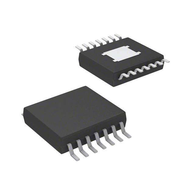
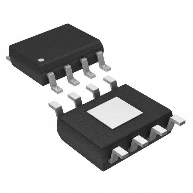
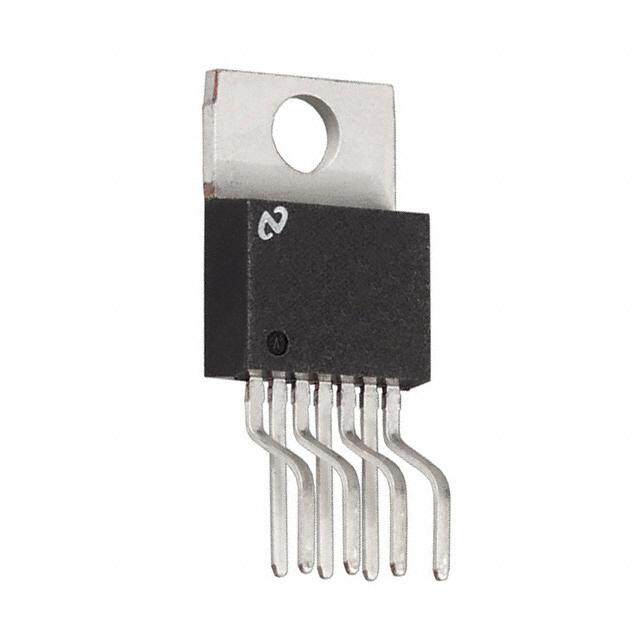
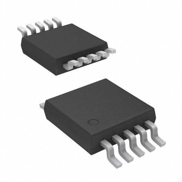
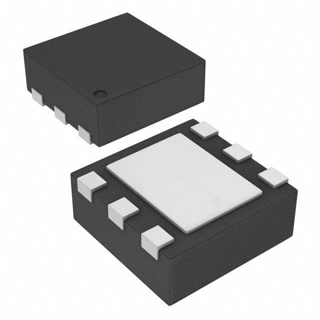
| 产品图片 |
|
| 产品型号 | LT3462ES6#TRMPBF |
| PWM类型 | 电流模式 |
| rohs | 无铅 / 符合限制有害物质指令(RoHS)规范要求 |
| 产品系列 | - |
| 供应商器件封装 | TSOT-23-6 |
| 其它名称 | LT3462ES6#TRMPBFDKR |
| 包装 | Digi-Reel® |
| 同步整流器 | 无 |
| 安装类型 | 表面贴装 |
| 封装/外壳 | SOT-23-6 细型,TSOT-23-6 |
| 工作温度 | -40°C ~ 85°C |
| 标准包装 | 1 |
| 电压-输入 | 2.5 V ~ 16 V |
| 电压-输出 | 可调至 -38V |
| 电流-输出 | 250mA |
| 类型 | 反相 |
| 输出数 | 1 |
| 输出类型 | 可调式 |
| 频率-开关 | 1.2MHz |



PDF Datasheet 数据手册内容提取
LT3462/LT3462A Inverting 1.2MHz/2.7MHz DC/DC Converters with Integrated Schottky FEATURES DESCRIPTION n Integrated Schottky Rectifier The LT®3462/LT3462A are general purpose fixed fre‑ n Fixed Frequency 1.2MHz/2.7MHz Operation quency current mode inverting DC/DC converters. Both n Very Low Noise: 1mV Output Ripple devices feature an integrated Schottky and a low V P-P CESAT n Low V Switch: 270mV at 250mA switch allowing a small converter footprint and lower CESAT n –5V at 100mA from 5V Input parts cost. The LT3462 switches at 1.2MHz while the n –12V at 30mA from 3.3V Input LT3462A switches at 2.7MHz. These high speeds enable n Low Input Bias Current GND Based FB Input the use of tiny, low cost and low height capacitors and n Low Impedance (40Ω) 1.265V Reference Output inductors. n High Output Voltage: Up to –38V The LT3462/LT3462A operate in a dual inductor inverting n Wide Input Range: 2.5V to 16V topology that filters both the input and output currents. n Uses Tiny Surface Mount Components Very low output voltage ripple approaching 1mV can P‑P n Low Shutdown Current: <10µA be achieved when ceramic capacitors are used. Fixed fre‑ n Low Profile (1mm) SOT‑23 (ThinSOT™) Package quency switching ensures a clean output free from low n 8‑Lead DFN (2mm × 2mm × 0.75mm) Package, frequency noise typically present with charge pump solu‑ LT3462A Only tions. The 40V switch allows a V to V differential of IN OUT up to 38V for dual inductor topologies. APPLICATIONS Both devices provide a low impedance 1.265V reference output to supply the feedback resistor network. A ground n CCD Bias referenced, high impedance FB input allows high feedback n LCD Bias resistor values without compromising output accuracy. n GaAs FET Bias n General Purpose Negative Voltage Supply All registered trademarks and trademarks are the property of their respective owners. TYPICAL APPLICATION 5V to –5V, 100mA Inverting DC/DC Converter Efficiency 75 22µH 1µF 22µH TA = 25°C VIN VIN = 5V 5V VOUT 70 –5V %) VIN = 3.3V SW D 267k 22pF 100mA CY ( 1µF VIN FB CIEN 65 LT3462A 68.1k 10µF EFFI SDREF 60 GND 3462 TA01 55 0 20 40 60 80 100 LOAD CURRENT (mA) 3462 TA01b Rev A 1 Document Feedback For more information www.analog.com
LT3462/LT3462A ABSOLUTE MAXIMUM RATINGS (Note 1) Input Voltage (V ) ....................................................16V Maximum Junction Temperature ..........................125°C IN SW Voltage ...............................................................40V Storage Temperature Range .................. –65°C to 150°C D Voltage ...............................................................–40V Lead Temperature (Soldering, 10sec) SDREF, FB Voltage ...................................................2.5V (TSOT‑23 Package Only) ...................................300°C Operating Ambient Temperature Range (Note 3) ................–40°C to 85°C PIN CONFIGURATION TOP VIEW TOP VIEW FB 1 8 SDREF GND 2 7 D SW 1 6 VIN 9 GND 2 5 D GND 3 6 NC FB 3 4 SDREF SW 4 5 VIN S6 PACKAGE DC PACKAGE (LT3462A ONLY) 6-LEAD PLASTIC TSOT-23 8-LEAD (2mm × 2mm) PLASTIC DFN TJMAX = 125°C, θJA = 192°C/W TJMAX = 125°C, θJA = 88.5°C/W EXPOSED PAD (PIN 9) IS GND ORDER INFORMATION http://www.linear.com/product/LT3462#orderinfo LEAD FREE FINISH TAPE AND REEL PART MARKING PACKAGE DESCRIPTION TEMPERATURE RANGE LT3462ES6#PBF LT3462ES6#TRPBF LTBBV 6‑Lead Plastic TSOT‑23 –40°C to 85°C LT3462AES6#PBF LT3462AES6#TRPBF LTBGB 6‑Lead Plastic TSOT‑23 –40°C to 85°C LT3462AEDC#PBF LT3462AEDC#TRPBF LHGH 8‑Lead (2mm × 2mm) Plastic DFN –40°C to 85°C Consult ADI Marketing for parts specified with wider operating temperature ranges. For more information on lead free part marking, go to: http://www.linear.com/leadfree/ For more information on tape and reel specifications, go to: http://www.linear.com/tapeandreel/. Some packages are available in 500 unit reels through designated sales channels with #TRMPBF suffix. Rev A 2 For more information www.analog.com
LT3462/LT3462A ELECTRICAL CHARACTERISTICS The l denotes the specifications which apply over the full operating temperature range, otherwise specifications are at T = 25°C, V = 3V, unless otherwise noted. A IN PARAMETER CONDITIONS MIN TYP MAX UNITS Minimum Operating Voltage 2.5 V Maximum Operating Voltage 16 V SDREF Voltage 10µA > I ≥ –80µA ● 1.245 1.265 1.285 V SDREF FB Pin Bias Current (Note 2) 15 50 nA SDREF Minus FB Voltage 10µA > I ≥ –80µA ● 1.235 1.263 1.285 V SDREF Error Amp Offset Voltage –12 12 mV SDREF Reference Source Current SDREF >1.2V ● 120 180 µA Supply Current FB = –0.05V, Not Switching 2.9 3.6 mA SDREF = 0V, FB = Open, V = 5V 6.5 10 µA IN SDREF Line Regulation 0.007 %/V Switching Frequency (LT3462) ● 0.8 1.2 1.6 MHz Switching Frequency (LT3462A) ● 2.0 2.7 3.5 MHz Maximum Duty Cycle (LT3462) ● 90 % Maximum Duty Cycle (LT3462A) ● 77 % Switch Current Limit 300 420 mA Switch V I = 250mA 270 350 mV CESAT SW Switch Leakage Current V = 5V 0.01 1 µA SW Rectifier Leakage Current V = –40V 0.03 4 µA D Rectifier Forward Drop I = 250mA 800 1100 mV SCHOTTKY SDREF Voltage Low ● 0.20 V SDREF Off‑State Pull‑Up Current 1 2 3 µA SDREF Turn‑Off Current –300 –200 µA Note 1: Stresses beyond those listed under Absolute Maximum Ratings Note 3: The LT3462E is guaranteed to meet specifications from 0°C to may cause permanent damage to the device. Exposure to any Absolute 70°C. Specifications over the –40°C to 85°C operating temperature range Maximum Rating condition for extended periods may affect device are assured by design, characterization and correlation with statistical reliability and lifetime. process controls. Note 2: Current flows out of the pin. Rev A 3 For more information www.analog.com
LT3462/LT3462A TYPICAL PERFORMANCE CHARACTERISTICS Oscillator Frequency (LT3462) Current Limit SDREF Minus FB Pin Voltage 1.6 480 1.29 TA = 25°C 1.5 LT3462 1.28 360 MHz) 1.4 T (mA) LT3462A FB (V) 1.27 FREQUENCY ( 11..32 CURRENT LIMI 240 SDREF MINUS 11..2265 120 1.1 1.24 1.0 0 1.23 –40 –20 0 20 40 60 80 100 10 20 30 40 50 60 70 80 90 –40 –20 0 20 40 60 80 100 TEMPERATURE (°C) DUTY CYCLE (%) TEMPERATURE (°C) 3462 G01 3462 G02 3462 G03 Quiescent Current in Oscillator Frequency (LT3462A) FB Bias Current Shutdown Mode 3.2 0 10 TA = 25°C TA = 25°C –5 FB = N/C 3.0 –10 8 FREQUENCY (MHz) 222...864 FB BIAS CURRENT (nA) –––––1223350505 QUIESCENT CURRENT (A) 64 –40 2 2.2 –45 2.0 –50 0 –40 –20 0 20 40 60 80 100 –40 –20 0 20 40 60 80 100 0 4 8 12 16 TEMPERATURE (°C) TEMPERATURE (°C) SUPPLY VOLTAGE (V) 3462 G04 3462 G05 3462 G06 PIN FUNCTIONS (TSOT-23/DFN) SW (Pin 1/Pin 4): Switch Pin. Connect to external induc‑ regulator. At turn‑on, a 180µA internal source pulls the tor L1 and positive terminal of transfer cap. pin to the regulation voltage. The SDREF pin can supply up to 80µA at 1.265V to bias the feedback resistor divider. GND (Pin 2/Pins 2, 3): Ground. Tie directly to local An optional soft‑start circuit capacitor connects from this ground plane. pin to –V . OUT FB (Pin 3/Pin 1): Feedback Pin. Connect resistive divider D (Pin 5/Pin 7): Anode Terminal of Integrated Schottky tap here. Set R1 according to R1 = R2 • (V /1.265V). OUT Diode. Connect to negative terminal of transfer cap and In shutdown, a proprietary shutdown bias current cancel‑ external inductor L2. lation circuit allows the internal 3µA source to pull up the SDREF pin, even with residual negative voltage on V . V (Pin 6/Pin 5): Input Supply Pin. Must be locally OUT IN bypassed. SDREF (Pin 4/Pin 8): Dual Function Shutdown and 1.265V Reference Output Pin. Pull to GND with exter‑ Exposed Pad (NA/Pin 9): GND. The exposed pad should nal N‑FET to turn regulator off. Turn‑off pull‑down and be soldered to the PCB ground to achieve the rated ther‑ a 2µA internal source will pull SDREF up to turn‑on the mal performance. Rev A 4 For more information www.analog.com
LT3462/LT3462A BLOCK DIAGRAM SW D – A1 DRIVER – E AMP FB + RC +COAM2P R S Q Q1 DO CC LG SHUTDOWN + BIAS CURRENT CANCELLATION 0.1Ω ISRC – OFF 3µA ON 180µA RAMP GND SDREF GENERATOR SHUTDOWN VOUT VOUT 1.2MHz* OSCILLATOR R1 (EXTERNAL) CS1 (EXTERNAL) *LT3462A IS 2.7MHz FB SDREF – R2 (EXTERNAL) CS2 (EXTERNAL) Q2 SDREF VIN 1.265V + CS1, CS2 OPTIONAL SOFT-START COMPONENTS REFERENCE 3462 F01 Figure 1. Block Diagram OPERATION The LT3462 uses a constant frequency, current mode of the PWM comparator. This current limit cell protects control scheme to provide excellent line and load regula‑ the power switch as well as various external components tion. Operation can be best understood by referring to the connected to the LT3462. Block Diagram in Figure 1. At the start of each oscillator SDREF is a dual function input pin. When driven low it cycle, the SR latch is set, turning on the power switch shuts the part down, reducing quiescent supply current Q1. A voltage proportional to the switch current is added to less than 10µA. When not driven low, the SDREF pin to a stabilizing ramp and the resulting sum is fed into has an internal pull‑up current that turns the regulator on. the positive terminal of the PWM comparator. When this Once the part is enabled, the SDREF pin sources up to voltage exceeds the voltage at the output of the EAMP, the 180µA nominally at a fixed voltage of 1.265V through SR latch is reset, turning off the power switch. The level external resistor R2 to FB. If there is no fault condition at the output of the EAMP is simply an amplified version present, FB will regulate to 0V, and V will regulate to OUT of the difference between the feedback voltage and GND. 1.265V • (–R1/R2). An optional soft‑start circuit uses the In this manner, the error amplifier sets the correct peak fixed SDREF pull‑up current and a capacitor from SDREF current level to keep the output in regulation. If the error to V to set the dV/dt on V . In shutdown, an FB bias OUT OUT amplifier’s output increases, more current is taken from current cancellation circuit supplies up to 150µA biasing the output; if it decreases, less current is taken. One func‑ current to external resistor R1 while V is lower than OUT tion not shown in Figure 1 is the current limit. The switch FB. This function eliminates R2 loading of SDREF during current is constantly monitored and not allowed to exceed shutdown. As a result, supply current in shutdown may the nominal value of 400mA. If the switch current reaches exceed 10µA by the amount of current flowing in R1. 400mA, the SR latch is reset regardless of the output state Rev A 5 For more information www.analog.com
LT3462/LT3462A APPLICATIONS INFORMATION Inrush Current Capacitor Selection The LT3462 has a built‑in Schottky diode. When supply Ceramic capacitors are recommended. An X7R or X5R voltage is applied to the V pin, the voltage difference dielectric should be used to avoid capacitance decreasing IN between V and V generates inrush current flowing severely with applied voltage and at temperature limits. IN D from input through the inductor and the Schottky diode The “flying” capacitor between the SW and D pins should to charge the flying capacitor to V . The maximum non‑ be a ceramic type of value 1µF or more. When used in IN repetitive surge current the Schottky diode in the LT3462 the dual inductor or coupled inductor topologies the fly‑ can sustain is 1.5A. The selection of inductor and capaci‑ ing capacitor should have a voltage rating that is more tor value should ensure the peak of the inrush current to than the difference between the input and output voltages. be below 1.5A. The peak inrush current can be calculated For the charge pump inverter topology, the voltage rat‑ as follows: ing should be more than the output voltage. The output capacitor should be a ceramic type. Acceptable output ⎛ ⎞ capacitance varies from 1µF for high V (–36V), to 10µF OUT V –0.6 ⎜ π ⎟ for low V (–5V). The input capacitor should be a 1µF IP= INL exp⎜– L ⎟ ceramic tOyUpTe and be placed as close as possible to the –1 ⎜ 2 –1⎟ LT3462/LT3462A. C ⎝ C ⎠ Layout Hints where L is the inductance between supply and SW, and C is the capacitance between SW and D. The high speed operation of the LT3462 demands care‑ ful attention to board layout. You will not get advertised Table 3 gives inrush peak currents for some component performance with careless layout. Figure 2 shows the rec‑ selections. ommended component placement. A ceramic capacitor Table 3. Inrush Peak Current of 1µF or more must be placed close to the IC for input V (V) L (µH) C (µF) I (A) supply bypassing. IN P 5 22 1 0.70 5 33 1 0.60 C1 12 47 1 1.40 + GND L1 Inductor Selection VIN C2 Each of the two inductors used with LT3462 should have 1 6 a saturation current rating (where inductance is approxi‑ 2 5 mately 70% of zero current inductance ) of approximately 3 4 L2 0.25A or greater. If the device is used in the charge pump C3 R2 mode, where there is only one inductor, then its rating should be 0.35A or greater. DCR of the inductors should R1 C4 be less than 1Ω. For LT3462, a value of 22µH is suitable VOUT if using a coupled inductor such as Sumida CLS62‑220. 3462 F02 If using two separate inductors, increasing the value to 47µH will result in the same ripple current. For LT3462A, Figure 2. Suggested Layout a value of 10µH for the coupled inductor and 22µH for two inductors will be acceptable for most applications. Rev A 6 For more information www.analog.com
LT3462/LT3462A TYPICAL APPLICATIONS 3.3V to –12V with Soft-Start Circuit –12V Efficiency 80 C2 L1 1µF L2 TA = 25°C 47µH 47µH VIN 75 3.3V VIN = 3.3V V–1O2UVT %) 70 C1 VSIWN DFB R2617k C154pF C23.302mµFA CIENCY ( 65 4.7µF LT3462 R2 C10S01nF EFFI 60 27.4k SDREF GND 55 OFF M1 22nF 50 C1: TAIYO YUDEN X5R JMK212BJ475MG 0 5 10 15 20 25 30 35 3462 TA02a C2: TAIYO YUDEN X5R EMK212BJ105MG LOAD CURRENT (mA) 3462 TA02b C3: TAIYO YUDEN EMK316BJ225 L1, L2: MURATA LQH32CN470 V Reaches –12V in 750µs; Input V Reaches –12V in 7.5ms; Input OUT OUT Current Peaks at 300mA without CS1 Current Peaks at 125mA with CS1 = 100nF OFF OFF VOUT VOUT 10V/DIV 10V/DIV 100mA/DIIIVN 50mA/DIIIVN 2ms/DIV 3462 TA02c 2ms/DIV 3462 TA02d Li+ to –8V Supply –8V Efficiency C2 80 L1A 1µF L1B TA = 25°C 22µH 22µH VIN 75 2.7V VIN = 3.3V TO 4.2V VOUT %) 70 C1 VSIWN DFB R2617k C154pF –8V CIENCY ( 65 4.7µF FI LT3462 R2 C3 EF 60 42.2k 4.7µF SDREF GND 55 50 C1: TAIYO YUDEN X5R JMK212BJ475MG 0 10 20 30 40 50 3462 TA03a C2: TAIYO YUDEN X5R EMK212BJ105MG LOAD CURRENT (mA) 3462 TA03b C3: TAIYO YUDEN LMK316BJ475 L1: SUMIDA CLS62-220 OR 2X MURATA LQH32CN330 Rev A 7 For more information www.analog.com
LT3462/LT3462A TYPICAL APPLICATIONS 3.3V to –8V (LT3462A) 5V to –5V Supply (LT3462A) C2 C2 L1A L1B L1 L2 1µF 1µF 10µH 10µH 22µH 22µH VIN VIN 2.7V 5V TO 4.2V VOUT V–5OVUT –8V R1 C4 35mA R1 C4 100mA SW D 267k 22pF SW D 267k 22pF C3 C1 VIN FB C1 VIN FB 10µF 1µF 1µF LT3462A R2 C3 LT3462A R2 42.2k 4.7µF 68.1k SDREF SDREF GND GND C1: TAIYO YUDEN JMK107BJ105MA 3462 TA04a C1: TAIYO YUDEN JMK107BJ105MA 3462 TA05a C2: TAIYO YUDEN EMK212BJ105MA C2: TAIYO YUDEN EMK212BJ105MA C3: TAIYO YUDEN LMK316BJ475 C3: MURATA GRM219R60J106KE19B L1: WURTH 50310057-100 L1, L2: MURATA LQH32CN220 Switching Waveform INDUCTOR 50mA/DIV VSW 10V/DIV VOUT 1mV/DIV AC‑COUPLED 3462 TA05b 200ns/DIV Rev A 8 For more information www.analog.com
LT3462/LT3462A PACKAGE DESCRIPTION Please refer to http://www.linear.com/product/LT3462#packaging for the most recent package drawings. DC8 Package 8-Lead Plastic DFN (2mm × 2mm) (Reference LTC DWG # 05-08-1719 Rev A) 0.70 ±0.05 2.55 ±0.05 1.15 ±0.050.64 ±0.05 (2 SIDES) PACKAGE OUTLINE 0.25 ±0.05 0.45 BSC 1.37 ±0.05 (2 SIDES) RECOMMENDED SOLDER PAD PITCH AND DIMENSIONS APPLY SOLDER MASK TO AREAS THAT ARE NOT SOLDERED R = 0.115 TYP R = 0.05 5 8 TYP 0.40 ±0.10 2.00 ±0.10 0.64 ±0.10 PIN 1 NOTCH PIN 1 BAR (4 SIDES) (2 SIDES) R = 0.20 OR TOP MARK 0.25 × 45° (SEE NOTE 6) CHAMFER (DC8) DFN 0409 REVA 4 1 0.23 ±0.05 0.200 REF 0.75 ±0.05 0.45 BSC 1.37 ±0.10 (2 SIDES) 0.00 – 0.05 BOTTOM VIEW—EXPOSED PAD NOTE: 1. DRAWING IS NOT A JEDEC PACKAGE OUTLINE 2. DRAWING NOT TO SCALE 3. ALL DIMENSIONS ARE IN MILLIMETERS 4. DIMENSIONS OF EXPOSED PAD ON BOTTOM OF PACKAGE DO NOT INCLUDE MOLD FLASH. MOLD FLASH, IF PRESENT, SHALL NOT EXCEED 0.15mm ON ANY SIDE 5. EXPOSED PAD SHALL BE SOLDER PLATED 6. SHADED AREA IS ONLY A REFERENCE FOR PIN 1 LOCATION ON THE TOP AND BOTTOM OF PACKAGE Rev A 9 For more information www.analog.com
LT3462/LT3462A PACKAGE DESCRIPTION Please refer to http://www.linear.com/product/LT3462#packaging for the most recent package drawings. S6 Package 6-Lead Plastic TSOT-23 (Reference LTC DWG # 05-08-1636) 2.90 BSC 0.62 0.95 (NOTE 4) MAX REF 1.22 REF 1.50 – 1.75 3.85 MAX 2.62 REF 1.4 MIN 2.80 BSC (NOTE 4) PIN ONE ID RECOMMENDED SOLDER PAD LAYOUT 0.30 – 0.45 0.95 BSC PER IPC CALCULATOR 6 PLCS (NOTE 3) 0.80 – 0.90 0.20 BSC 0.01 – 0.10 1.00 MAX DATUM ‘A’ 0.30 – 0.50 REF 1.90 BSC 0.09 – 0.20 (NOTE 3) S6 TSOT-23 0302 NOTE: 1. DIMENSIONS ARE IN MILLIMETERS 2. DRAWING NOT TO SCALE 3. DIMENSIONS ARE INCLUSIVE OF PLATING 4. DIMENSIONS ARE EXCLUSIVE OF MOLD FLASH AND METAL BURR 5. MOLD FLASH SHALL NOT EXCEED 0.254mm 6. JEDEC PACKAGE REFERENCE IS MO-193 Rev A 10 For more information www.analog.com
LT3462/LT3462A REVISION HISTORY REV DATE DESCRIPTION PAGE NUMBER A 05/18 Add 2mm × 2mm 8‑lead DFN package information (A‑grade version only) to data sheet 1, 2, 4, 9 Rev A 11 Information furnished by Analog Devices is believed to be accurate and reliable. However, no responsibility is assumed by Analog Devices for its use, nor for any infringements of patents or other rights of third parties that may result from its use. Specifications subject to change without notice. No license Fiso gr rmanoterde biyn fimorpmlicaattiioonn owr wotwhe.arwniasleo ugn.cdoerm any patent or patent rights of Analog Devices.
LT3462/LT3462A TYPICAL APPLICATION 12V to –36V DC/DC Converter –36V Efficiency L1 C2 85 47µH 0.47µF D1 TA = 25°C VIN 12V 80 VIN = 12V VOUT –36V %) SW D R4312k C4 36mA CY ( 75 C1 VIN FB 5pF EN 1µF CI LT3462 R2 C3 FFI 70 15k 1µF E SDREF 50V GND 65 100nF 60 C1: TAIYO YUDEN X5R EMK212BJ105 3462 TA06a 0 10 20 30 40 C2: MURATA GRM42-6X7R474K50 LOAD CURRENT (mA) C3: MURATA GRM42-6X7R474K50 ×2 D1: CENTRAL CMSH5-4-LTN 3462 TA06b L1: MURATA LQH32CN470 RELATED PARTS PART NUMBER DESCRIPTION COMMENTS LT1617/LT1617‑1 350mA/100mA (I ) High Efficiency Micropower V : 1.2V to 15V, V = –34V, I = 20µA, I <1µA ThinSOT Package SW IN OUT(MAX) Q SD Inverting DC/DC Converter LT1931/LT1931A 1A (I ), 1.2MHz/2.2MHz, High Efficiency V : 2.6V to 16V, V = –34V, I = 5.8mA, I <1µA ThinSOT Package SW IN OUT(MAX) Q SD Micropower Inverting DC/DC Converter LT1945 Dual Output, Boost/Inverter, 350mA (I ), Constant V : 1.2V to 15V, V = ±34V, I = 40µA, I <1µA, MS10 Package SW IN OUT(MAX) Q SD Off‑Time, High Efficiency Step‑Up DC/DC Converter LT1946/LT1946A 1.5A (I ), 1.2MHz/2.7MHz, High Efficiency Step‑Up V : 2.45V to 16V, V = 34V, I = 3.2mA, I <1µA MS8 Package SW IN OUT(MAX) Q SD DC/DC Converter LT3463 Dual Output, Boost/Inverter, 250mA (I ), Constant V : 2.3V to 15V, V = ±40V, I = 40µA, I <1µA DFN Package SW IN OUT(MAX) Q SD Off‑Time, High Efficiency Step‑Up DC/DC Converter with Integrated Schottky Diodes LT3464 85mA (I ), High Efficiency Step‑Up DC/DC V : 2.3V to 10V, V = 34V, I = 25µA, I <1µA ThinSOT Package SW IN OUT(MAX) Q SD Converter with Integrated Schottky and PNP Disconnect Rev A 12 D16961-0-5/18(A) www.analog.com ANALOG DEVICES, INC. 2004-2018

 Datasheet下载


