ICGOO在线商城 > 集成电路(IC) > PMIC - 稳压器 - 线性 > LT3082ITS8#TRMPBF

 Datasheet下载
- 型号: LT3082ITS8#TRMPBF
- 制造商: LINEAR TECHNOLOGY
- 库位|库存: xxxx|xxxx
- 要求:
| 数量阶梯 | 香港交货 | 国内含税 |
| +xxxx | $xxxx | ¥xxxx |
查看当月历史价格
查看今年历史价格
LT3082ITS8#TRMPBF产品简介:
ICGOO电子元器件商城为您提供LT3082ITS8#TRMPBF由LINEAR TECHNOLOGY设计生产,在icgoo商城现货销售,并且可以通过原厂、代理商等渠道进行代购。 LT3082ITS8#TRMPBF价格参考。LINEAR TECHNOLOGYLT3082ITS8#TRMPBF封装/规格:PMIC - 稳压器 - 线性, Linear Voltage Regulator IC Positive Adjustable 1 Output 0 V ~ 38.5 V 200mA TSOT-23-8。您可以下载LT3082ITS8#TRMPBF参考资料、Datasheet数据手册功能说明书,资料中有LT3082ITS8#TRMPBF 详细功能的应用电路图电压和使用方法及教程。
LT3082ITS8#TRMPBF 是 Linear Technology(现为 Analog Devices)生产的一款高性能、双通道、低压差线性稳压器(LDO)。以下是该型号的应用场景:

 1. 工业自动化
   - 应用场景:在工业控制设备中,如可编程逻辑控制器(PLC)、数据采集系统(DAQ)和传感器接口。
   - 特点:LT3082 提供高精度输出电压调节能力,适合需要稳定电源的工业环境。其低噪声特性有助于减少对敏感模拟信号的干扰。

 2. 通信设备
   - 应用场景:适用于基站、路由器、交换机等通信设备中的射频(RF)模块和数字信号处理单元。
   - 特点:双通道设计允许同时为 RF 前端和数字电路供电,确保两者之间的电气隔离并降低相互干扰。

 3. 医疗电子
   - 应用场景:用于便携式医疗设备(如心率监测仪、血糖仪)以及诊断设备(如超声波机)。
   - 特点:低噪声和高 PSRR(电源抑制比)特性使其非常适合为高灵敏度的医疗传感器和放大器供电。

 4. 汽车电子
   - 应用场景:车载信息娱乐系统、导航系统、ADAS(高级驾驶辅助系统)以及车身控制模块。
   - 特点:宽输入电压范围(1.2V 至 40V)使其能够承受汽车电池的瞬态电压波动,而其内置保护功能(如过流保护和热关断)增强了可靠性。

 5. 测试与测量仪器
   - 应用场景:示波器、信号发生器、精密电源等测试设备。
   - 特点:支持高达 2A 的输出电流,且具备出色的负载和线路调整率,确保测试结果的准确性。

 6. 消费类电子产品
   - 应用场景:高端音频设备(如耳机放大器、DAC 模块)和智能家居设备。
   - 特点:极低的输出噪声(通常小于 20µV RMS)使它成为对音质要求较高的应用的理想选择。

 总结
LT3082ITS8#TRMPBF 凭借其双通道输出、低噪声、高 PSRR 和宽输入电压范围等特点,在需要高精度和稳定性电源供应的各种领域中表现出色。无论是工业、通信还是消费类市场,这款器件都能满足严苛的设计需求。
| 参数 | 数值 |
| 产品目录 | 集成电路 (IC) |
| 描述 | IC REG LDO ADJ 0.2A TSOT23-8 |
| 产品分类 | |
| 品牌 | Linear Technology |
| 数据手册 | http://www.linear.com/docs/28489 |
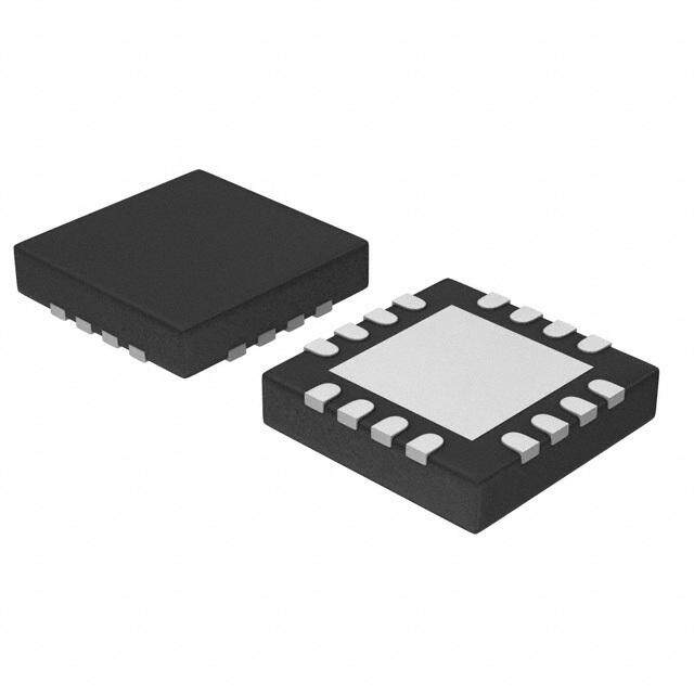
| 产品图片 |
|
| 产品型号 | LT3082ITS8#TRMPBF |
| rohs | 无铅 / 符合限制有害物质指令(RoHS)规范要求 |
| 产品系列 | - |
| 产品培训模块 | http://www.digikey.cn/PTM/IndividualPTM.page?site=cn&lang=zhs&ptm=21623 |
| 供应商器件封装 | TSOT-23-8 |
| 其它名称 | LT3082ITS8#TRMPBFCT |
| 包装 | 剪切带 (CT) |
| 安装类型 | 表面贴装 |
| 封装/外壳 | SOT-23-8 薄型,TSOT-23-8 |
| 工作温度 | -40°C ~ 125°C |
| 标准包装 | 1 |
| 特色产品 | http://www.digikey.cn/product-highlights/cn/zh/linear-technology-ldo-linear-regulators/2739 |
| 电压-跌落(典型值) | 1.3V @ 200mA |
| 电压-输入 | 1.2 V ~ 40 V |
| 电压-输出 | 0 V ~ 38.5 V |
| 电流-输出 | 200mA |
| 电流-限制(最小值) | 200mA |
| 稳压器拓扑 | 正,可调式 |
| 稳压器数 | 1 |


- 商务部:美国ITC正式对集成电路等产品启动337调查
- 曝三星4nm工艺存在良率问题 高通将骁龙8 Gen1或转产台积电
- 太阳诱电将投资9.5亿元在常州建新厂生产MLCC 预计2023年完工
- 英特尔发布欧洲新工厂建设计划 深化IDM 2.0 战略
- 台积电先进制程称霸业界 有大客户加持明年业绩稳了
- 达到5530亿美元!SIA预计今年全球半导体销售额将创下新高
- 英特尔拟将自动驾驶子公司Mobileye上市 估值或超500亿美元
- 三星加码芯片和SET,合并消费电子和移动部门,撤换高东真等 CEO
- 三星电子宣布重大人事变动 还合并消费电子和移动部门
- 海关总署:前11个月进口集成电路产品价值2.52万亿元 增长14.8%


PDF Datasheet 数据手册内容提取
LT3082 200mA Single Resistor Low Dropout Linear Regulator FEATURES DESCRIPTION n Outputs May Be Paralleled for Higher Output The LT®3082 is a 200mA low dropout linear regulator that Current or Heat Spreading can be paralleled to increase output current or spread heat n Maximum Output Current: 200mA in surface mounted boards. Architected as a precision n Wide Input Voltage Range: 1.2V to 40V current source and voltage follower, this regulator benefi ts n Output Adjustable to 0V many applications requiring high current, adjustability to n Stable with Minimum 2.2μF Ceramic Capacitors zero and no heat sink. The LT3082 withstands reverse n Single Resistor Sets Output Voltage input voltages and reverse output-to-input voltages without n Initial Set Pin Current Accuracy: 1% reverse-current fl ow. n Low Output Noise: 33μV (10Hz to 100kHz) RMS A key feature of the LT3082 is the capability to supply a n Reverse-Battery Protection wide output voltage range. A precision “0” TC 10μA ref- n Reverse-Current Protection erence current source drives a single resistor to program n <1mV Load Regulation Typical the output voltage to any level between zero and 38.5V. n <0.001%/V Line Regulation Typical The LT3082 is stable with only 2.2μF of capacitance on n Current Limit and Thermal Shutdown Protection the output; the IC uses small ceramic capacitors that n Available in 8-Lead SOT-23, 3-Lead SOT-223 and do not require additional ESR as is common with other 8-Lead 3mm × 3mm DFN Packages regulators. APPLICATIONS Internal protection circuitry includes reverse-battery and reverse-current protection, current limiting and ther- n All-Surface Mount Power Supply mal limiting. The LT3082 is offered in the thermally en- n Post Regulator for Switching Supplies hanced 8-lead TSOT-23, 3-lead SOT-223 and 8-lead 3mm n Low Parts Count Variable Voltage Supply × 3mm DFN packages. n Low Output Voltage Supply n Battery Powered Regulator L, LT, LTC, LTM, Linear Technology and the Linear logo are registered trademarks of Linear Technology Corporation. All other trademarks are the property of their respective owners. TYPICAL APPLICATION SET Pin Current vs Temperature Variable Output Voltage Battery Powered Supply 10.100 10.075 IN LT3082 A) 10.050 9V 1μF 10μA T (μ 10.025 N E + R R 10.000 U – PIN C 9.975 T E SET OUT S 9.950 VOUT= 10μA • RSET 9.925 CSET RSET COUT 0.1μF 500k 2.2μF 9.900 –50 –25 0 25 50 75 100 125 150 TEMPERATURE (°C) 3082 TA01a 3082 TA01b 3082f 1
LT3082 ABSOLUTE MAXIMUM RATINGS (Note 1) All Voltages Relative to V OUT IN Pin Voltage Relative to SET, OUT ........................±40V Operating Junction Temperature Range (Notes 2, 8) SET Pin Current (Note 6) .....................................±15mA E, I Grades .........................................–40°C to 125°C SET Pin Voltage (Relative to OUT, Note 6) ...............±10V MP Grade ...........................................–55°C to 125°C Output Short-Circuit Duration ..........................Indefi nite Storage Temperature Range ...................–65°C to 150°C Lead Temperature (ST, TS8 Packages Only) Soldering, 10 sec ..............................................300°C PIN CONFIGURATION TOP VIEW TOP VIEW 3 IN TOP VIEW OUT 1 8 IN OUT 2 9 7 IN TAB IS OUT 2 OUT ONUCT 12 87 IINN NC 3 6 NC OUT 3 6 NC SET 4 5 NC 1 SET OUT 4 5 SET ST PACKAGE TS8 PACKAGE DD PACKAGE 3-LEAD PLASTIC SOT-223 8-LEAD PLASTIC TSOT-23 8-LEAD (3mm (cid:115) 3mm) PLASTIC DFN TJMAX = 125°C, θJA = 28°C/W, θJC = 3°C/W TAB IST OJMUATX, M= U12S5T° BCE, θSJOA L=D 2E4R°ECD/W T,O θ JOCU =T 1O5N°C T/HWE PCB; TJMAX = 125°C, θJA = 57°C/W, θJC = 15°C/W EXPOSED PAD (PIN 9) IS OUT, MUST BE SOLDERED TO OUT ON SEE THE APPLICATIONS INFORMATION SECTION THE PCB; SEE THE APPLICATIONS INFORMATION SECTION ORDER INFORMATION LEAD FREE FINISH TAPE AND REEL PART MARKING* PACKAGE DESCRIPTION TEMPERATURE RANGE LT3082EDD#PBF LT3082EDD#TRPBF LDYT 8-Lead (3mm × 3mm) Plastic DFN –40°C to 125°C LT3082IDD#PBF LT3082IDD#TRPBF LDYT 8-Lead (3mm × 3mm) Plastic DFN –40°C to 125°C LT3082EST#PBF LT3082EST#TRPBF 3082 3-Lead Plastic SOT-223 –40°C to 125°C LT3082IST#PBF LT3082IST#TRPBF 3082 3-Lead Plastic SOT-223 –40°C to 125°C LT3082MPST#PBF LT3082MPST#TRPBF 3082MP 3-Lead Plastic SOT-223 –55°C to 125°C LT3082ETS8#PBF LT3082ETS8#TRPBF LTDYV 8-Lead Plastic SOT-23 –40°C to 125°C LT3082ITS8#PBF LT3082ITS8#TRPBF LTDYV 8-Lead Plastic SOT-23 –40°C to 125°C LEAD BASED FINISH TAPE AND REEL PART MARKING* PACKAGE DESCRIPTION TEMPERATURE RANGE LT3082EDD LT3082EDD#TR LDYT 8-Lead (3mm × 3mm) Plastic DFN –40°C to 125°C LT3082IDD LT3082IDD#TR LDYT 8-Lead (3mm × 3mm) Plastic DFN –40°C to 125°C LT3082EST LT3082EST#TR 3082 3-Lead Plastic SOT-223 –40°C to 125°C LT3082IST LT3082IST#TR 3082 3-Lead Plastic SOT-223 –40°C to 125°C LT3082MPST LT3082MPST#TR 3082MP 3-Lead Plastic SOT-223 –55°C to 125°C LT3082ETS8 LT3082ETS8#TR LTDYV 8-Lead Plastic SOT-23 –40°C to 125°C LT3082ITS8 LT3082ITS8#TR LTDYV 8-Lead Plastic SOT-23 –40°C to 125°C Consult LTC Marketing for parts specifi ed with wider operating temperature ranges. *The temperature grade is identifi ed by a label on the shipping container. For more information on lead free part marking, go to: http://www.linear.com/leadfree/ For more information on tape and reel specifi cations, go to: http://www.linear.com/tapeandreel/ 3082f 2
LT3082 ELECTRICAL CHARACTERISTICS The l denotes the specifi cations which apply over the full operating temperature range, otherwise specifi cations are at T = 25°C. (Note 2) J PARAMETER CONDITIONS MIN TYP MAX UNITS SET Pin Current I V = 2V, I = 1mA 9.90 10 10.10 μA SET IN LOAD 2V ≤ V ≤ 40V, 1mA ≤ I ≤ 200mA l 9.80 10 10.20 μA IN LOAD Offset Voltage (V – V ) V V = 2V, I = 1mA –2 2 mV OUT SET OS IN LOAD V = 2V, I = 1mA l –4 4 mV IN LOAD Load Regulation (Note 7) ΔI ΔI = 1mA to 200mA –0.1 nA SET LOAD ΔV ΔI = 1mA to 200mA l –0.5 –2 mV OS LOAD Line Regulation ΔI ΔV = 2V to 40V, I = 1mA 0.03 0.2 nA/V SET IN LOAD ΔV ΔV = 2V to 40V, I = 1mA 0.003 0.010 mV/V OS IN LOAD Minimum Load Current (Note 3) 2V ≤ V ≤ 40V l 300 500 μA IN Dropout Voltage (Note 4) I = 10mA l 1.22 1.45 V LOAD I = 200mA l 1.3 1.65 V LOAD Current Limit V = 5V, V = 0V, V = –0.1V l 200 300 mA IN SET OUT Error Amplifi er RMS Output Noise (Note 5) I = 200mA, 10Hz ≤ f ≤ 100kHz, C = 10μF, 33 μV LOAD OUT RMS C = 0.1μF SET Reference Current RMS Output Noise (Note 5) 10Hz ≤ f ≤ 100kHz 0.7 nA RMS Ripple Rejection f = 120Hz, V = 0.5V , I = 0.1A, 90 dB RIPPLE P-P LOAD C = 2.2μF, C = 0.1μF OUT SET f = 10kHz 75 dB f = 1MHz 20 dB Thermal Regulation I 10ms Pulse 0.003 %/W SET Note 1: Stresses beyond those listed under Absolute Maximum Ratings Note 4: For the LT3082, dropout is specifi ed as the minimum input-to- may cause permanent damage to the device. Exposure to any Absolute output voltage differential required supplying a given output current. Maximum Rating condition for extended periods may affect device Note 5: Adding a small capacitor across the reference current resistor reliability and lifetime. lowers output noise. Adding this capacitor bypasses the resistor shot Note 2: Unless otherwise specifi ed, all voltages are with respect to V . noise and reference current noise; output noise is then equal to error OUT The LT3082E is tested and specifi ed under pulse load conditions such amplifi er noise (see the Applications Information section). that TJ ≅ TA. The LT3082E is 100% tested at TA = 25°C. Performance at Note 6: Diodes with series 1k resistors clamp the SET pin to the OUT pin. –40°C and 125°C is assured by design, characterization, and correlation These diodes and resistors only carry current under transient overloads. with statistical process controls. The LT3082I is guaranteed to meet all Note 7: Load regulation is Kelvin-sensed at the package. data sheet specifi cations over the full –40°C to 125°C operating junction Note 8: This IC includes overtemperature protection that protects the temperature range. The LT3082MP is 100% tested and guaranteed over device during momentary overload conditions. Junction temperature the –55°C to 125°C operating junction temperature range. exceeds the maximum operating junction temperature when Note 3: Minimum load current is equivalent to the quiescent current of overtemperature protection is active. Continuous operation above the the part. Since all quiescent and drive current is delivered to the output specifi ed maximum operating junction temperature may impair device of the part, the minimum load current is the minimum current required to reliability. maintain regulation. 3082f 3
LT3082 TYPICAL PERFORMANCE CHARACTERISTICS SET Pin Current SET Pin Current Distribution Offset Voltage (V – V ) OUT SET 10.100 2.0 N = 1326 10.075 1.5 A)10.050 V) 1.0 RENT (μ10.025 AGE (m 0.5 ET PIN CUR190..907050 FFSET VOLT–0.50 S 9.950 O–1.0 9.925 –1.5 9.900 –2.0 –50 –25 0 25 50 75 100 125 150 9.80 9.90 10 10.10 10.20 –50 –25 0 25 50 75 100 125 150 TEMPERATURE (°C) SET PIN CURRENT DISTRIBUTION (μA) TEMPERATURE (°C) 3082 G01 3082 G03 3082 G02 Offset Voltage Distribution Offset Voltage Offset Voltage 1.00 100 N = 1326 ILOAD = 1mA 50 0.75 0 0.50 mV) μV) –50 GE ( 0.25 GE (–100 OLTA 0 OLTA–150 OFFSET V––00..2550 OFFSET V––225000 –300 –0.75 –350 –1.00 –400 –2 –1 0 1 2 0 5 10 15 20 25 30 35 40 0 50 100 150 200 VOS DISTRIBUTION (mV) INPUT-TO-OUTPUT VOLTAGE (V) LOAD CURRENT (mA) 3082 G05 3082 G06 3082 G04 Load Regulation Minimum Load Current C GE WITH LOAD (μV)–11–050500000 ΔVIINLO –AC DVH O=AU N1TmG =EA 3 IVTNO R 2E0F0EmREANCE CURRENT –02–1201000HANGE IN REFERENC RRENT (μA) 546000000 A E U OLT–150 –30 CU D C 300 V R A OFFSET ––220500 (VOUT – VSET) ––4500RENT W MUM LO 200 CHANGE IN –––343005000 CHANGE IN OFFSET VOLTAGE –––867000ITH LOAD (nA MINI 1000 –50 –25 0 25 50 75 100 125 150 ) –50 –25 0 25 50 75 100 125 150 TEMPERATURE (°C) TEMPERATURE (°C) 3082 G08 3082 G07 3082f 4
LT3082 TYPICAL PERFORMANCE CHARACTERISTICS Dropout Voltage Dropout Voltage Current Limit 1.6 1.4 400 OLTAGE (V – V) (V)INOUT 01011.....82604 TTTJJJ === –215525°5C°°CC OLTAGE (V – V) (V)INOUT 1001....0682 IILLOOAADD == 120000mmAA RENT LIMIT (mA)231230055500000 V V R OUT 0.4 OUT 0.4 CU 100 P P O O DR 0.2 DR 0.2 50 TJ = 25°C 0 0 0 0 25 50 75 100 125 150 175 200 –50 –25 0 25 50 75 100 125 150 0 2 4 6 8 10 LOAD CURRENT (mA) TEMPERATURE (°C) INPUT-TO-OUTPUT DIFFERENTIAL VOLTAGE (V) 3082 G10 3082 G09 3082 G11 Current Limit Load Transient Response 500 200 450 V) m 400 N ( 150 O A) 350 ATI 100 T (m 300 DEVI 50 LIMI 250 AGE 0 URRENT 125000 UT VOLT––15000 CU C 10500 VVIONU =T =7 V0V OUTP–1500 50 1001502002503003504004505002050RRENT (mALOAD 0 TIME (μs) ) –50 –25 0 25 50 75 100 125 150 VOUT = 1V CSET = 0.1μF TEMPERATURE (°C) 3082 G12 CIN = 1μF CERAMIC ΔILOAD = 10mA to 200mA COUT = 2.2μF CERAMIC 3082 G13 Line Transient Response Turn-On Response 60 V) 2.0 VOLTAGEON (mV) 2400 OLTAGE ( 11..05 OUTPUT DEVIATI–200 UTPUT V 0.50 O –40 264 VOLTAGE (VINPUT 042 VOLTAGE (V)INPUT 0 ) 0 50 100150200250300350400450500 0 10 20 30 40 50 60 70 80 90 100 TIME (μs) TIME (μs) VOUT = 1V CSET = 0.1μF COUT = 2.2μF CERAMIC CSET = 0 CIN = 1μF CERAMIC ILOAD = 10mA RSET = 100k RLOAD = 5Ω COUT = 2.2μF CERAMIC 3082 G14 3082f 5
LT3082 TYPICAL PERFORMANCE CHARACTERISTICS Residual Output for Less Than Minimum Load Current Ripple Rejection Ripple Rejection (120Hz) 800 120 90 SET PIN = 0V 89 700 VIN VOUT VIN = 36V 100 88 AGE (mV) 650000 RTEST VIN = 5V TION (dB) 80 TION (dB) 8867 UT VOLT 430000 E REJEC 60 C0.S1EμTF = E REJEC 8845 UTP PPL 40 PPL 83 O 200 RI 20 VRIINP P=L VEO =U T5(0N0OmMVINPA-LP) + 3V CSET = 0 RI 82 VRIINP P=L VEO =U T5(0N0OmMVINPA-LP), +f =2 V120Hz 100 ILOAD = 200mA 81 ILOAD = 0.2A COUT = 2.2μF CSET = 0, COUT = 2.2μF 0 0 80 0 1000 2000 10 100 1k 10k 100k 1M 10M –50 –25 0 25 50 75 100 125 150 RTEST (Ω) 3082 G16 FREQUENCY (Hz) TEMPERATURE (°C) 3082 G18 3082 G17 Noise Spectral Density RE Output Voltage Noise F E 10k 1k R E NC VBAT = 3.6V V/√Hz) 1k 100 E CURR ICCCPPOO== 2 20.02μΩAF n E SITY ( NT NO 100μVV/ODUIVT OISE SPECTRAL DEN 10100 110.0 ISE SPECTRAL DENS TIME 1ms/DIV 3082 G20 N IT 1 0.1 Y (pA VROSUETT == 110V0k CILOOUATD == 22.020μmFA 10 100 1k 10k 100k /√H CSET = 0.1μF FREQUENCY (Hz) z) 3082 G19 3082f 6
LT3082 PIN FUNCTIONS (DD/ST/TS8) IN (Pins 7, 8/Pin 3/Pins 7, 8): Input. This pin supplies SET (Pin 4/Pin 1/Pin 5): Set. This pin is the error ampli- power to regulate internal circuitry and supply output load fi er’s noninverting input and also sets the operating bias current. For the device to operate properly and regulate, point of the circuit. A fi xed 10μA current source fl ows the voltage on this pin must be 1.2V to 1.4V above the out of this pin. A single external resistor programs V . OUT OUT pin (depending on output load current—see the Output voltage range is 0V to 38.5V. dropout voltage specifi cations in the Electrical Charac- Exposed Pad/Tab (Pin 9/Tab/NA): Output. The Exposed teristics table). Pad of the DFN package and the Tab of the SOT-223 NC (Pins 3, 5, 6/NA/Pins 1, 6): No Connection. These package are tied internally to OUT. Tie them directly to OUT pins have no connection to internal circuitry and may be pins (Pins 1, 2/Pin 2) at the PCB. The amount of copper area tied to IN, OUT, GND or fl oated. and planes connected to the Exposed Pad/Tab determine the effective thermal resistance of the packages (see the OUT (Pins 1, 2/Pin 2/Pins 2, 3, 4): Output. This is the Applications Information section). power output of the device. The LT3082 requires a 0.5mA minimum load current or the output will not regulate. BLOCK DIAGRAM IN 10μA + – SET OUT 3082 BD 3082f 7
LT3082 APPLICATIONS INFORMATION Introduction reference current source allows the regulator to have gain and frequency response independent of the impedance on The LT3082 regulator is easy to use and has all the pro- the positive input. On older adjustable regulators, such as tection features expected in high performance regulators. the LT1086, loop gain changes with output voltage and Included are reverse-input, reverse-output and reverse bandwidth changes if the adjustment pin is bypassed input-to-output protection for sensitive circuitry and loads. to ground. For the LT3082, loop gain is unchanged with Additional protection includes short-circuit protection and output voltage changes or bypassing. Output regulation thermal shutdown with hysteresis. is not a fi xed percentage of output voltage, but is a fi xed The LT3082 fi ts well in applications needing multiple rails. fraction of millivolts. Use of a true current source allows This new architecture adjusts down to zero with a single all of the gain in the buffer amplifi er to provide regulation, resistor, handling modern low voltage digital IC’s as well and none of that gain is needed to amplify up the reference as allowing easy parallel operation and thermal manage- to a higher output voltage. ment without heat sinks. Adjusting to zero output allows shutting off the powered circuitry. When the input is pre- Programming Output Voltage regulated—such as a 5V or 3.3V input supply—external The LT3082 generates a 10μA reference current that resistors can help spread the heat. fl ows out of the SET pin. Connecting a resistor from SET A precision “0” TC 10μA reference current source connects to GND generates a voltage that becomes the reference to the noninverting input of a power operational amplifi er. point for the error amplifi er (see Figure 1). The reference The power operational amplifi er provides a low impedance voltage equals 10μA multiplied by the value of the SET buffered output to the voltage on the noninverting input. pin resistor. Any voltage may be generated and there A single resistor from the noninverting input to ground is no minimum output voltage for the regulator. Table sets the output voltage. If this resistor is set to 0Ω, zero 1 lists many common output voltages and the closest output voltage results. Therefore, any output voltage be- standard 1% resistor values used to generate that output tween zero and the maximum defi ned by the input power voltage. supply voltage is obtainable. Regulation of the output voltage requires a minimum load The benefi t of using a true internal current source as the current of 0.5mA. For a true 0V output operation, return reference, as opposed to a bootstrapped reference in older this minimum 0.5mA load current to a negative supply regulators, is not so obvious in this architecture. A true voltage. IN LT3082 CIN 10μA + – SET OUT VOUT= 10μA • RSET CSET RSET COUT RLOAD 3082 F01 Figure 1. Basic Adjustable Regulator 3082f 8
LT3082 APPLICATIONS INFORMATION Table 1. 1% Resistors for Common Output Voltages If guard ring techniques are used, this bootstraps any V (V) R (k) stray capacitance at the SET pin. Since the SET pin is OUT SET 1 100 a high impedance node, unwanted signals may couple 1.2 121 into the SET pin and cause erratic behavior. This will 1.5 150 be most noticeable when operating with minimum 1.8 182 output capacitors at full load current. The easiest way to remedy this is to bypass the SET pin with a small 2.5 249 amount of capacitance from SET to ground; 10pF to 3.3 332 20pF is suffi cient. 5 499 Stability and Output Capacitance With a 10μA current source generating the reference The LT3082 requires an output capacitor for stability. It voltage, leakage paths to or from the SET pin can create is designed to be stable with most low ESR capacitors errors in the reference and output voltages. High qual- (typically ceramic, tantalum or low ESR electrolytic). A ity insulation should be used (e.g., Tefl on, Kel-F). The minimum output capacitor of 2.2μF with an ESR of 0.5Ω cleaning of all insulating surfaces to remove fl uxes and or less is recommended to prevent oscillations. Larger other residues may be required. Surface coating may be necessary to provide a moisture barrier in high humidity values of output capacitance decrease peak deviations environments. and provide improved transient response for larger load current changes. Bypass capacitors, used to decouple Minimize board leakage by encircling the SET pin and individual components powered by the LT3082, increase circuitry with a guard ring that is operated at a potential the effective output capacitor value. For improvement in close to itself. Tie the guard ring to the OUT pin. Guarding transient response performance, place a capacitor across both sides of the circuit board is required. Bulk leakage the voltage setting resistor. Capacitors up to 1μF can be reduction depends on the guard ring width. 10nA of leak- used. This bypass capacitor reduces system noise as well, age into or out of the SET pin and its associated circuitry but start-up time is proportional to the time constant of creates a 0.1% reference voltage error. Leakages of this the voltage setting resistor (R in Figure 1) and SET pin magnitude, coupled with other sources of leakage, can SET bypass capacitor. cause signifi cant offset voltage and reference drift, es- pecially over the possible operating temperature range. Give extra consideration to the use of ceramic capacitors. Figure 2 depicts an example guard ring layout. Ceramic capacitors are manufactured with a variety of di- OUT SET GND 3082 F02 Figure 2. Example Guard Ring Layout for DFN Package 3082f 9
LT3082 APPLICATIONS INFORMATION electrics, each with different behavior across temperature Stability and Input Capacitance and applied voltage. The most common dielectrics used Low ESR, ceramic input bypass capacitors are acceptable are specifi ed with EIA temperature characteristic codes of for applications without long input leads. However, applica- Z5U, Y5V, X5R and X7R. The Z5U and Y5V dielectrics are tions connecting a power supply to an LT3082 circuit’s IN good for providing high capacitances in a small package, and GND pins with long input wires combined with a low but they tend to have strong voltage and temperature ESR, ceramic input capacitors are prone to voltage spikes, coeffi cients, as shown in Figures 3 and 4. When used with reliability concerns and application-specifi c board oscil- a 5V regulator, a 16V 10μF Y5V capacitor can exhibit an lations. The input wire inductance found in many battery effective value as low as 1μF to 2μF for the DC bias voltage powered applications, combined with the low ESR ceramic applied and over the operating temperature range. The X5R input capacitor, forms a high-Q LC resonant tank circuit. In and X7R dielectrics result in more stable characteristics some instances this resonant frequency beats against the and are more suitable for use as the output capacitor. output current dependent LDO bandwidth and interferes The X7R type has better stability across temperature, with proper operation. Simple circuit modifi cations/solu- while the X5R is less expensive and is available in higher tions are then required. This behavior is not indicative of values. Care still must be exercised when using X5R and LT3082 instability, but is a common ceramic input bypass X7R capacitors. The X5R and X7R codes only specify capacitor application issue. operating temperature range and maximum capacitance change over temperature. Capacitance change due to DC The self-inductance, or isolated inductance, of a wire is bias with X5R and X7R capacitors is better than with Y5V directly proportional to its length. Wire diameter is not a and Z5U capacitors, but can still be signifi cant enough to major factor on its self-inductance. For example, the self- drop capacitor values below appropriate levels. Capacitor inductance of a 2-AWG isolated wire (diameter = 0.26") is DC bias characteristics tend to improve as component about half the self-inductance of a 30-AWG wire (diameter case size increases, but expected capacitance at operating = 0.01"). One foot of 30-AWG wire has about 465nH of voltage should be verifi ed. self-inductance. Voltage and temperature coeffi cients are not the only One of two ways reduces a wire’s self-inductance. One sources of problems. Some ceramic capacitors have a method divides the current fl owing towards the LT3082 piezoelectric response. A piezoelectric device generates between two parallel conductors. In this case, the farther voltage across its terminals due to mechanical stress. In a apart the wires are from each other, the more the self-in- ceramic capacitor, the stress can be induced by vibrations ductance is reduced; up to a 50% reduction when placed in the system or thermal transients. a few inches apart. Splitting the wires basically connects 20 40 BOTH CAPACITORS ARE 16V, 1210 CASE SIZE, 10μF 20 0 %) X5R %) 0 X5R E (–20 E ( U U L L –20 A A V V N –40 N GE I GE I –40 Y5V N N A–60 A H H –60 C Y5V C –80 –80 BOTH CAPACITORS ARE 16V, 1210 CASE SIZE, 10μF –100 –100 0 2 4 6 8 10 12 14 16 –50 –25 0 25 50 75 100 125 DC BIAS VOLTAGE (V) TEMPERATURE (°C) 3082 F03 3082 F04 Figure 3. Ceramic Capacitor DC Bias Characteristics Figure 4. Ceramic Capacitor Temperature Characteristics 3082f 10
LT3082 APPLICATIONS INFORMATION two equal inductors in parallel, but placing them in close Spreading the devices on the PC board also spreads the proximity gives the wires mutual inductance adding to heat. Series input resistors can further spread the heat if the self-inductance. The second and most effective way the input-to-output difference is high. to reduce overall inductance is to place both forward and return current conductors (the input and GND wires) in IN LT3082 very close proximity. Two 30-AWG wires separated by 10μA only 0.02", used as forward- and return-current conduc- + tors, reduce the overall self-inductance to approximately – one-fi fth that of a single isolated wire. SET OUT 50mΩ If wiring modifi cations are not permissible for the applica- tions, including series resistance between the power supply VIN IN LT3082 4.8V TO and the input of the LT3082 also stabilizes the application. 40V As little as 0.1Ω to 0.5Ω, often less, is effective in damping 10μA the LC resonance. If the added impedance between the + 1μF power supply and the input is unacceptable, adding ESR to – the input capacitor also provides the necessary damping of SET OUT the LC resonance. However, the required ESR is generally 50mΩ VOUT, 3.3V 0.4A higher than the series impedance required. 165k 10μF 3082 F05 Paralleling Devices Figure 5. Parallel Devices Higher output current is obtained by paralleling multiple LT3082s together. Tie the individual SET pins together and Quieting the Noise tie the individual IN pins together. Connect the outputs in The LT3082 offers numerous noise performance advan- common using small pieces of PC trace as ballast resistors tages. Every linear regulator has its sources of noise. In to promote equal current sharing. PC trace resistance in general, a linear regulator’s critical noise source is the mΩ/inch is shown in Table 2. Ballasting requires only a reference. In addition, consider the error amplifi er’s noise tiny area on the PCB. contribution along with the resistor divider’s noise gain. Table 2. PC Board Trace Resistance Many traditional low noise regulators bond out the voltage WEIGHT (oz) 10mil WIDTH 20mil WIDTH reference to an external pin (usually through a large value 1 54.3 27.1 resistor) to allow for bypassing and noise reduction. The 2 27.1 13.6 LT3082 does not use a traditional voltage reference like Trace resistance is measured in mΩ/in other linear regulators. Instead, it uses a 10μA reference The worst-case room temperature offset, only ±2mV current. The 10μA current source generates noise current between the SET pin and the OUT pin, allows the use of levels of 2.7pA/√Hz (0.7nA over the 10Hz to 100kHz RMS very small ballast resistors. bandwidth). The equivalent voltage noise equals the RMS noise current multiplied by the resistor value. As shown in Figure 5, each LT3082 has a small 50mΩ ballast resistor, which at full output current gives better The SET pin resistor generates spot noise equal to √4kTR than 80% equalized sharing of the current. The external (k = Boltzmann’s constant, 1.38 • 10–23J/°K, and T is abso- resistance of 50mΩ (25mΩ for the two devices in paral- lute temperature) which is RMS summed with the voltage lel) adds only about 10mV of output regulation drop at an noise If the application requires lower noise performance, output of 0.4A. Even with an output voltage as low as 1V, bypass the voltage/current setting resistor with a capacitor this adds only 1% to the regulation. Of course, paralleling to GND. Note that this noise-reduction capacitor increases more than two LT3082s yields even higher output current. start-up time as a factor of the RC time constant. 3082f 11
LT3082 APPLICATIONS INFORMATION The LT3082 uses a unity-gain follower from the SET pin IN LT3082 to the OUT pin. Therefore, multiple possibilities exist (besides a SET pin resistor) to set output voltage. For 10μA example, using a high accuracy voltage reference from + SET to GND removes the errors in output voltage due to – PARASITIC reference current tolerance and resistor tolerance. Active RESISTANCE SET OUT driving of the SET pin is acceptable. RP The typical noise scenario for a linear regulator is that the RSET RP LOAD output voltage setting resistor divider gains up the noise 3082 F06 RP reference, especially if V is much greater than V . The OUT REF LT3082’s noise advantage is that the unity-gain follower presents no noise gain whatsoever from the SET pin to the Figure 6. Connections for Best Load Regulation output. Thus, noise fi gures do not increase accordingly. Error amplifi er noise is typical 100nV/√Hz (33μV over RMS Thermal Considerations the 10Hz to 100kHz bandwidth). The error amplifi er’s noise is RMS summed with the other noise terms to give a fi nal The LT3082’s internal power and thermal limiting circuitry noise fi gure for the regulator. protects itself under overload conditions. For continuous normal load conditions, do not exceed the 125°C maximum Curves in the Typical Performance Characteristics sec- junction temperature. Carefully consider all sources of tion show noise spectral density and peak-to-peak noise thermal resistance from junction-to-ambient. This includes characteristics for both the reference current and error (but is not limited to) junction-to-case, case-to-heat sink amplifi er over the 10Hz to 100kHz bandwidth. interface, heat sink resistance or circuit board-to-ambient as the application dictates. Consider all additional, adjacent Load Regulation heat generating sources in proximity on the PCB. The LT3082 is a fl oating device. No ground pin exists on Surface mount packages provide the necessary heatsinking the packages. Thus, the IC delivers all quiescent current by using the heat spreading capabilities of the PC board, and drive current to the load. Therefore, it is not possible copper traces and planes. Surface mount heat sinks, plated to provide true remote load sensing. The connection resis- through-holes and solder-fi lled vias can also spread the tance between the regulator and the load determines load heat generated by power devices. regulation performance. The data sheet’s load regulation specifi cation is Kelvin sensed at the package’s pins. Nega- Junction-to-case thermal resistance is specifi ed from tive-side sensing is a true Kelvin connection by returning the IC junction to the bottom of the case directly, or the bottom of the voltage setting resistor to the negative the bottom of the pin most directly, in the heat path. side of the load (see Figure 6). This is the lowest thermal resistance path for heat fl ow. Only proper device mounting ensures the best possible Connected as shown, system load regulation is the sum thermal fl ow from this area of the package to the heat of the LT3082’s load regulation and the parasitic line sinking material. resistance multiplied by the output current. To minimize load regulation, keep the positive connection between the Note that the Exposed Pad of the DFN package and the regulator and load as short as possible. If possible, use tab of the SOT-223 package is electrically connected to large diameter wire or wide PC board traces. the output (V ). OUT 3082f 12
LT3082 APPLICATIONS INFORMATION Tables 3 through 5 list thermal resistance as a function PCB layers, copper weight, board layout and thermal vias of copper areas in a fi xed board size. All measurements affect the resultant thermal resistance. Please reference were taken in still air on a 4-layer FR-4 board with 1oz JEDEC standard JESD51-7 for further information on high solid internal planes and 2oz external trace planes with a thermal conductivity test boards. Achieving low thermal total fi nished board thickness of 1.6mm. resistance necessitates attention to detail and careful layout. Demo circuit 1447A’s board layout using multiple inner Table 3. DD Package, 8-Lead DFN V planes and multiple thermal vias achieves 28°C/W OUT COPPER AREA THERMAL RESISTANCE performance for the DFN package. TOPSIDE* BACKSIDE BOARD AREA (JUNCTION-TO-AMBIENT) 2500mm2 2500mm2 2500mm2 25°C/W Calculating Junction Temperature 1000mm2 2500mm2 2500mm2 25°C/W Example: Given an industrial factory application with an 225mm2 2500mm2 2500mm2 28°C/W input voltage of 15V ±10%, an output voltage of 12V ±5%, 100mm2 2500mm2 2500mm2 32°C/W an output current of 200mA and a maximum ambient *Device is mounted on topside temperature of 50°C, what would be the maximum junc- tion temperature for a DFN package? Table 4. TS8 Package, 8-Lead SOT-23 The total circuit power equals: COPPER AREA THERMAL RESISTANCE TOPSIDE* BACKSIDE BOARD AREA (JUNCTION-TO-AMBIENT) P = (V – V )(I ) TOTAL IN OUT OUT 2500mm2 2500mm2 2500mm2 54°C/W The SET pin current is negligible and can be ignored. 1000mm2 2500mm2 2500mm2 54°C/W 225mm2 2500mm2 2500mm2 57°C/W VIN(MAX CONTINUOUS) = 16.5 (15V + 10%) 100mm2 2500mm2 2500mm2 63°C/W V = 11.4V (12V – 5%) OUT(MIN CONTINUOUS) *Device is mounted on topside I = 200mA OUT Table 5. ST Package, 3-Lead SOT-223 Power dissipation under these conditions equals: COPPER AREA THERMAL RESISTANCE P = (16.5 – 11.4V)(200mA) = 1.02W TOTAL TOPSIDE* BACKSIDE BOARD AREA (JUNCTION-TO-AMBIENT) 2500mm2 2500mm2 2500mm2 20°C/W Junction temperature equals: 1000mm2 2500mm2 2500mm2 20°C/W TJ = TA + PTOTAL • θJA 225mm2 2500mm2 2500mm2 24°C/W T = 50°C + (1.02W • 30°C/W) = 80.6°C 100mm2 2500mm2 2500mm2 29°C/W J *Device is mounted on topside In this example, junction temperature is below the maxi- mum rating, ensuring reliable operation. For further information on thermal resistance and using thermal information, refer to JEDEC standard JESD51, notably JESD51-12. 3082f 13
LT3082 APPLICATIONS INFORMATION Protection Features greater than IN, is less than 1mA (typically under 100μA), protecting the LT3082 and sensitive loads. The LT3082 incorporates several protection features ideal for battery-powered circuits, among other applications. In Clamping diodes and 1k limiting resistors protect the addition to normal monolithic regulator protection features LT3082’s SET pin relative to the OUT pin voltage. These such as current limiting and thermal limiting, the LT3082 protection components typically only carry current under protects itself against reverse-input voltages, reverse- transient overload conditions. These devices are sized to output voltages, and reverse OUT-to-SET pin voltages. handle ±10V differential voltages and ±15mA crosspin current fl ow without concern. Relative to these application Current limit protection and thermal overload protection concerns, note the following two scenarios. The fi rst sce- protect the IC against output current overload conditions. nario employs a noise-reducing SET pin bypass capacitor For normal operation, do not exceed a junction temperature while OUT is instantaneously shorted to GND. The second of 125°C. The thermal shutdown circuit’s temperature scenario follows improper shutdown techniques in which threshold is typically 165°C and incorporates about 5°C the SET pin is reset to GND quickly while OUT is held up of hysteresis. by a large output capacitance with light load. The Typical The LT3082’s IN pin withstands ±40V voltages with respect Applications section shows simple, robust techniques for to the OUT and SET pins. Reverse current fl ow, if OUT is shutting down SET and OUT together. TYPICAL APPLICATIONS DAC-Controlled Regulator Two-Level Regulator IN LT3082 IN LT3082 VIN VIN 10μA 10μA + + 150k 450k – – –LT1991 SET OUT VOUT SET OUT VOUT SPI 150k LTC2641 + 4.7μF R2 2.2μF 3082 TA02 3082 TA03 GAIN = 4 VN2222LL R1 3082f 14
LT3082 TYPICAL APPLICATIONS Using a Lower Value SET Resistor LT3082 VIN IN 12V 10μA + – C1 VOUT 1μF SET OUT 0.5V TO 10V VOUT = 0.5V + 1mA • RSET R1 R2 49.9k 1mA 499Ω 1% 1% RSET COUT 10k 4.7μF 3082 TA04 Adding Soft-Start LT3082 VIN IN 4.8V to 40V 10μA + C1 D1 1μF 1N4148 – VOUT 3.3V SET OUT 0.2A C2 R1 COUT 0.01μF 332k 4.7μF 3082 TA05 Coincident Tracking LT3082 IN 10μA LT3082 IN + – 10μA VOUT3 VIN IN LT3082 + SET OUT 50V.2A 7V TO 40V C4 – R3 4.7μF 10μA 169k V3.O3UVT2 3082 TA06 SET OUT + 0.2A C3 – R2 4.7μF C1 80.6k VOUT1 1.5μF 2.5V SET OUT 0.2A C2 R1 4.7μF 249k 3082f 15
LT3082 TYPICAL APPLICATIONS Adding Shutdown Reference Buffer LT3082 IN LT3082 VIN VIN IN 10μA 10μA + + – – SET OUT SET OUT ON OFF QVN12222LL R1 QVN2*2222LLVOUT LT10I1N9PUTOUTPUT C1 C4.27μFVOUT* GND SHUTDOWN 1μF * MINIMUM LOAD 0.5mA 3082 TA07 3082 TA08 *Q2 INSURES ZERO OUTPUT IN THE ABSENCE OF ANY OUTPUT LOAD. High Voltage Regulator 6.1V VIN 10k 50V 1N4148 LT3082 IN BUZ11 10μA + 10μF + – VOUT VOUT= 20V + SET OUT 0.2A VOUT = 10μA • RSET 15μF RSET 4.7μF 2MEG 3082 TA09 Ramp Generator LT3082 VIN IN 5V 10μA + 1μF – SET OUT VOUT VN2222LL 1nF VN2222LL 4.7μF 3082 TA10 3082f 16
LT3082 PACKAGE DESCRIPTION DD Package 8-Lead Plastic DFN (3mm × 3mm) (Reference LTC DWG # 05-08-1698) 0.675 ±0.05 3.5 ±0.05 1.65 ±0.05 2.15 ±0.05 (2 SIDES) PACKAGE OUTLINE 0.25 ± 0.05 0.50 BSC 2.38 ±0.05 (2 SIDES) RECOMMENDED SOLDER PAD PITCH AND DIMENSIONS R = 0.115 0.38 ± 0.10 TYP 5 8 3.00 ±0.10 1.65 ± 0.10 (4 SIDES) (2 SIDES) PIN 1 TOP MARK (NOTE 6) (DD) DFN 1203 4 1 0.200 REF 0.75 ±0.05 0.25 ± 0.05 0.50 BSC 2.38 ±0.10 (2 SIDES) 0.00 – 0.05 BOTTOM VIEW—EXPOSED PAD NOTE: 1. DRAWING TO BE MADE A JEDEC PACKAGE OUTLINE M0-229 VARIATION OF (WEED-1) 2.DRAWING NOT TO SCALE 3. ALL DIMENSIONS ARE IN MILLIMETERS 4. DIMENSIONS OF EXPOSED PAD ON BOTTOM OF PACKAGE DO NOT INCLUDE MOLD FLASH. MOLD FLASH, IF PRESENT, SHALL NOT EXCEED 0.15mm ON ANY SIDE 5. EXPOSED PAD SHALL BE SOLDER PLATED 6.SHADED AREA IS ONLY A REFERENCE FOR PIN 1 LOCATION ON TOP AND BOTTOM OF PACKAGE 3082f 17
LT3082 PACKAGE DESCRIPTION ST Package 3-Lead Plastic SOT-223 (Reference LTC DWG # 05-08-1630) .248 – .264 .129 MAX (6.30 – 6.71) .114 – .124 .059 MAX (2.90 – 3.15) .264 – .287 .248 BSC (6.70 – 7.30) .130 – .146 (3.30 – 3.71) .039 MAX .059 MAX .090 BSC .181 MAX .0905 .033 – .041 RECOMMENDED SOLDER PAD LAYOUT (2.30) (0.84 – 1.04) BSC 10° – 16° .010 – .014 .071 10° (0.25 – 0.36) (1.80) MAX MAX 10° – 16° .024 – .033 .012 .0008 – .0040 (0.60 – 0.84) (0.31) (0.0203 – 0.1016) .181 MIN (4.60) ST3 (SOT-233) 0502 BSC 3082f 18
LT3082 PACKAGE DESCRIPTION TS8 Package 8-Lead Plastic TSOT-23 (Reference LTC DWG # 05-08-1637) 2.90 BSC 0.52 0.65 (NOTE 4) MAX REF 1.22 REF 1.50 – 1.75 3.85 MAX2.62 REF 1.4 MIN 2.80 BSC (NOTE 4) PIN ONE ID RECOMMENDED SOLDER PAD LAYOUT 0.22 – 0.36 0.65 BSC PER IPC CALCULATOR 8 PLCS (NOTE 3) 0.80 – 0.90 0.20 BSC 0.01 – 0.10 1.00 MAX DATUM ‘A’ 0.30 – 0.50 REF 1.95 BSC 0.09 – 0.20 (NOTE 3) TS8 TSOT-23 0802 NOTE: 1. DIMENSIONS ARE IN MILLIMETERS 2. DRAWING NOT TO SCALE 3. DIMENSIONS ARE INCLUSIVE OF PLATING 4. DIMENSIONS ARE EXCLUSIVE OF MOLD FLASH AND METAL BURR 5. MOLD FLASH SHALL NOT EXCEED 0.254mm 6. JEDEC PACKAGE REFERENCE IS MO-193 3082f Information furnished by Linear Technology Corporation is believed to be accurate and reliable. 19 However, no responsibility is assumed for its use. Linear Technology Corporation makes no representa- tion that the interconnection of its circuits as described herein will not infringe on existing patent rights.
LT3082 TYPICAL APPLICATIONS Active-Driven Regulator LT3082 VIN IN 10μA + – ⎛ R2 ⎞ OUT VOUT=⎝⎜R1+R2⎠⎟•V1+10µA•(R1||R2) SET V1 R1, 100k VOUT 0V TO 5V 0.5V TO 3V R2 2.2μF 100k 3082 TA11 RELATED PARTS PART NUMBER DESCRIPTION COMMENTS LT1761 100mA, Low Noise LDO 300mV Dropout Voltage, Low Noise = 20μV , V : 1.8V to 20V, ThinSOT™ Package RMS IN LT1762 150mA, Low Noise LDO 300mV Dropout Voltage, Low Noise = 20μV , V : 1.8V to 20V, MS-8 Package RMS IN LT1763 500mA, Low Noise LDO 300mV Dropout Voltage, Low Noise = 20μV , V : 1.8V to 20V, SO-8 Package RMS IN LT1962 300mA, Low Noise LDO 270mV Dropout Voltage, Low Noise = 20μV , V : 1.8V to 20V, MS-8 Package RMS IN LT1964 200mA, Low Noise, Negative LDO 340mV Dropout Voltage, Low Noise = 30μV , V : –1.8V to –20V, ThinSOT Package RMS IN LT3008 20mA, 45V, 3μA I Micropower 280mV Dropout Voltage, Low I = 3μA, V : 2V to 45V, V : 0.6V to 39.5V; Q Q IN OUT LDO ThinSOT and 2mm × 2mm DFN-6 Packages LT3009 20mA, 3μA I Micropower LDO 280mV Dropout Voltage, Low I = 3μA, V : 1.6V to 20V, V : 0.6V to 19.5V; Q Q IN OUT ThinSOT and SC-70 Packages LT3010 50mA, High Voltage, Micropower V : 3V to 80V, V : 1.275V to 60V, V = 0.3V, I = 30μA, I <1μA, IN OUT DO Q SD LDO Low Noise <100μV , Stable with 1μF Output Capacitor, Exposed MS8 Package RMS LT3011 50mA, High Voltage, Micropower V : 3V to 80V, V : 1.275V to 60V, V = 0.3V, I = 46μA, I <1μA, IN OUT DO Q SD LDO with Power Good Low Noise <100μV , Power Good, Stable with 1μF Output Capacitor, RMS 3mm × 3mm DFN-10 and Exposed MS-12E Packages LT3012 250mA, 4V to 80V, Low Dropout V : 4V to 80V, V : 1.24V to 60V, V = 0.4V, I = 40μA, I <1μA, IN OUT DO Q SD Micropower Linear Regulator TSSOP-16E and 4mm × 3mm DFN-12 Packages LT3013 250mA, 4V to 80V, Low Dropout V : 4V to 80V, V : 1.24V to 60V, V = 0.4V, I = 65μA, I <1μA, Power Good; IN OUT DO Q SD Micro-power Linear Regulator TSSOP-16E and 4mm × 3mm DFN-12 Packages with PWRGD LT3014/LT3014HV 20mA, 3V to 80V, Low Dropout V : 3V to 80V (100V for 2ms, HV Version), V : 1.22V to 60V, V = 0.35V, I = 7μA, IN OUT DO Q Micropower Linear Regulator I <1μA, ThinSOT and 3mm × 3mm DFN-8 Packages SD LT3020 100mA, Low Voltage VLDO Linear V : 0.9V to 10V, V : 0.2V to 5V (Min), V = 0.15V, I = 120μA, Noise <250μV , IN OUT DO Q RMS Regulator Stable with 2.2μF Ceramic Capacitors, DFN-8 and MS-8 Packages LT3021 500mA, Low Voltage, Very Low V : 0.9V to 10V, Dropout Voltage = 160mV (Typical), Adjustable Output (V = V IN REF OUT(MIN) Dropout VLDO Linear Regulator = 200mV), Fixed Output Voltages: 1.2V, 1.5V, 1.8V, Stable with Low ESR, Ceramic Output Capacitors 16-Pin 5mm × 5mm DFN and 8-Lead SO Packages LT3080/LT3080-1 1.1A, Parallelable, Low Noise, 300mV Dropout Voltage (2-Supply Operation), Low Noise = 40μV , V : 1.2V to 36V, RMS IN Low Dropout Linear Regulator V : 0V to 35.7V, Current-Based Reference with 1-Resistor V Set; Directly Parallelable OUT OUT (No Op Amp Required), Stable with Ceramic Capacitors; TO-220, SOT-223, MSOP-8 and 3mm × 3mm DFN-8 Packages; LT3080-1 Version Has Integrated Internal Ballast Resistor LT3085 500mA, Parallelable, Low Noise, 275mV Dropout Voltage (2-Supply Operation), Low Noise: 40μV , V : 1.2V to 36V, RMS IN Low Dropout Linear Regulator V : 0V to 35.7V, Current-Based Reference with 1-Resistor V Set; Directly Parallelable (No OUT OUT Op Amp Required), Stable with Ceramic Capacitors; MSOP-8 and 2mm × 3mm DFN-6 Packages ThinSOT is a trademark of Linear Technology Corporation. 3082f 20 Linear Technology Corporation LT 0709 • PRINTED IN USA 1630 McCarthy Blvd., Milpitas, CA 95035-7417 (408) 432-1900 ● FAX: (408) 434-0507 ● www.linear.com © LINEAR TECHNOLOGY CORPORATION 2009
Mouser Electronics Authorized Distributor Click to View Pricing, Inventory, Delivery & Lifecycle Information: A nalog Devices Inc.: LT3082ITS8#TRPBF LT3082EST#TRPBF LT3082MPST#TRPBF LT3082ETS8#TRPBF LT3082IDD#TRPBF LT3082MPST#TR LT3082IDD LT3082ITS8#PBF LT3082MPST LT3082EDD#TRPBF LT3082IST#TRPBF LT3082ETS8#PBF LT3082MPST#PBF LT3082ITS8#TRMPBF LT3082IST#PBF LT3082EST#PBF LT3082ETS8#TRMPBF LT3082EDD#PBF LT3082IDD#PBF