ICGOO在线商城 > 集成电路(IC) > PMIC - 稳压器 - 线性 > LT3080EST#TRPBF

 Datasheet下载
- 型号: LT3080EST#TRPBF
- 制造商: LINEAR TECHNOLOGY
- 库位|库存: xxxx|xxxx
- 要求:
| 数量阶梯 | 香港交货 | 国内含税 |
| +xxxx | $xxxx | ¥xxxx |
查看当月历史价格
查看今年历史价格
LT3080EST#TRPBF产品简介:
ICGOO电子元器件商城为您提供LT3080EST#TRPBF由LINEAR TECHNOLOGY设计生产,在icgoo商城现货销售,并且可以通过原厂、代理商等渠道进行代购。 LT3080EST#TRPBF价格参考。LINEAR TECHNOLOGYLT3080EST#TRPBF封装/规格:PMIC - 稳压器 - 线性, Linear Voltage Regulator IC Positive Adjustable 1 Output 1.1A SOT-223-3。您可以下载LT3080EST#TRPBF参考资料、Datasheet数据手册功能说明书,资料中有LT3080EST#TRPBF 详细功能的应用电路图电压和使用方法及教程。
| 参数 | 数值 |
| 产品目录 | 集成电路 (IC) |
| 描述 | IC REG LDO ADJ 1.1A SOT223 |
| 产品分类 | |
| 品牌 | Linear Technology |
| 数据手册 | http://www.linear.com/docs/25276 |
| 产品图片 |
|
| 产品型号 | LT3080EST#TRPBF |
| rohs | 无铅 / 符合限制有害物质指令(RoHS)规范要求 |
| 产品系列 | - |
| 产品培训模块 | http://www.digikey.cn/PTM/IndividualPTM.page?site=cn&lang=zhs&ptm=11978http://www.digikey.cn/PTM/IndividualPTM.page?site=cn&lang=zhs&ptm=30565 |
| 产品目录页面 | |
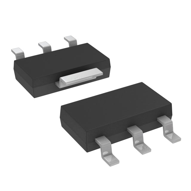
| 供应商器件封装 | SOT-223 |
| 其它名称 | LT3080EST#TRPBF-ND |
| 包装 | 带卷 (TR) |
| 安装类型 | 表面贴装 |
| 封装/外壳 | TO-261-4,TO-261AA |
| 工作温度 | -40°C ~ 125°C |
| 标准包装 | 2,000 |
| 特色产品 | http://www.digikey.com/cn/zh/ph/LT/lt3080.htmlhttp://www.digikey.cn/product-highlights/cn/zh/linear-technology-ldo-linear-regulators/2739 |
| 电压-跌落(典型值) | 1.35V @ 1.1A |
| 电压-输入 | 1.2 V ~ 36 V |
| 电压-输出 | 可调至 36V |
| 电流-输出 | 1.1A |
| 电流-限制(最小值) | 1.1A |
| 稳压器拓扑 | 正,可调式 |
| 稳压器数 | 1 |
| 视频文件 | http://www.digikey.cn/classic/video.aspx?PlayerID=1364138032001&width=640&height=505&videoID=602021950001http://www.digikey.cn/classic/video.aspx?PlayerID=1364138032001&width=640&height=505&videoID=602031206001 |
| 配用 | /product-detail/zh/DC995A/DC995A-ND/4866662 |


- 商务部:美国ITC正式对集成电路等产品启动337调查
- 曝三星4nm工艺存在良率问题 高通将骁龙8 Gen1或转产台积电
- 太阳诱电将投资9.5亿元在常州建新厂生产MLCC 预计2023年完工
- 英特尔发布欧洲新工厂建设计划 深化IDM 2.0 战略
- 台积电先进制程称霸业界 有大客户加持明年业绩稳了
- 达到5530亿美元!SIA预计今年全球半导体销售额将创下新高
- 英特尔拟将自动驾驶子公司Mobileye上市 估值或超500亿美元
- 三星加码芯片和SET,合并消费电子和移动部门,撤换高东真等 CEO
- 三星电子宣布重大人事变动 还合并消费电子和移动部门
- 海关总署:前11个月进口集成电路产品价值2.52万亿元 增长14.8%


PDF Datasheet 数据手册内容提取
LT3080 Adjustable1.1A Single Resistor Low Dropout Regulator FeaTures DescripTion n Outputs May be Paralleled for Higher Current and The LT®3080 is a 1.1A low dropout linear regulator that can Heat Spreading be paralleled to increase output current or spread heat in n Output Current: 1.1A surface mounted boards. Architected as a precision cur- n Single Resistor Programs Output Voltage rent source and voltage follower allows this new regulator n 1% Initial Accuracy of SET Pin Current to be used in many applications requiring high current, n Output Adjustable to 0V adjustability to zero, and no heat sink. Also the device n Low Output Noise: 40µV (10Hz to 100kHz) brings out the collector of the pass transistor to allow low RMS n Wide Input Voltage Range: 1.2V to 36V dropout operation —down to 350 millivolts— when used n Low Dropout Voltage: 350mV (Except SOT-223 with multiple supplies. Package) A key feature of the LT3080 is the capability to supply a n <1mV Load Regulation wide output voltage range. By using a reference current n <0.001%/V Line Regulation through a single resistor, the output voltage is programmed n Minimum Load Current: 0.5mA to any level between zero and 36V. The LT3080 is stable n Stable with 2.2µF Minimum Ceramic Output Capacitor with 2.2µF of capacitance on the output, and the IC uses n Current Limit with Foldback and Overtemperature small ceramic capacitors that do not require additional Protected ESR as is common with other regulators. n Available in 8-Lead MSOP, 3mm × 3mm DFN, 5-Lead DD-Pak, TO-220 and 3-Lead SOT-223 Internal protection circuitry includes current limiting and thermal limiting. The LT3080 regulator is offered in the applicaTions 8-lead MSOP (with an exposed pad for better thermal characteristics), a 3mm × 3mm DFN, 5-lead DD-Pak, n High Current All Surface Mount Supply TO-220 and a simple-to-use 3-lead SOT-223 version. n High Efficiency Linear Regulator n Post Regulator for Switching Supplies L, LT, LTC, LTM, Linear Technology and the Linear logo are registered trademarks and VLDO and ThinSOT are trademarks of Linear Technology Corporation. All other trademarks are the n Low Parts Count Variable Voltage Supply property of their respective owners. n Low Output Voltage Power Supplies Typical applicaTion Set Pin Current Distribution Variable Output Voltage 1.1A Supply N = 13792 VIN IN LT3080 1.2V TO 36V VCONTROL + – 1µF OUT VOUT SET 2.2µF RSET VOUT = RSET • 10µA 9.80 9.90 10.00 10.10 10.20 3080 TA01a SET PIN CURRENT DISTRIBUTION (µA) 3080 G02 3080fc 1
LT3080 absoluTe MaxiMuM raTings (Note 1)(All Voltages Relative to V ) OUT V Pin Voltage .....................................40V, –0.3V Operating Junction Temperature Range (Notes 2, 10) CONTROL IN Pin Voltage ................................................40V, –0.3V E-, I-Grades ............................................–40°C to 125°C SET Pin Current (Note 7) .....................................±10mA Storage Temperature Range: ..................–65°C to 150°C SET Pin Voltage (Relative to OUT) .........................±0.3V Lead Temperature (Soldering, 10 sec) Output Short-Circuit Duration ..........................Indefinite MS8E, Q, T and ST Packages Only ....................300°C pin conFiguraTion TOP VIEW FRONT VIEW TOP VIEW OUT 1 8 IN 5 IN OUT 1 8IN OUT 2 9 7 IN OUT 2 9 7IN TAB IS 4 VCONTROL OUT 3 OUT 6 NC OUT 3 OUT 6NC OUT 3 OUT SET 4 5 VCONTROL SET 4 5VCONTROL 2 SET MS8E PACKAGE 1 NC 8-LEAD PLASTIC MSOP DD PACKAGE TJMAX = 125°C, θJA = 60°C/W, θJC = 10°C/W Q PACKAGE 8-LEAD (3mm × 3mm) PLASTIC DFN EXPOSED PAD (PIN 9) IS OUT, MUST BE SOLDERED TO PCB 5-LEAD PLASTIC DD-PAK TJMAX = 125°C, θJA = 64°C/W, θJC = 3°C/W TJMAX = 125°C, θJA = 30°C/W, θJC = 3°C/W EXPOSED PAD (PIN 9) IS OUT, MUST BE SOLDERED TO PCB FRONT VIEW FRONT VIEW 3 IN* 5 IN 4 VCONTROL TAB IS TAB IS OUT 2 OUT OUT 3 OUT 2 SET 1 SET 1 NC ST PACKAGE T PACKAGE 3-LEAD PLASTIC SOT-223 5-LEAD PLASTIC TO-220 *IN IS VCONTROL AND IN TIED TOGETHER TJMAX = 125°C, θJA = 40°C/W, θJC = 3°C/W TJMAX = 125°C, θJA = 55°C/W, θJC = 15°C/W 3080fc 2
LT3080 orDer inForMaTion LEAD FREE FINISH TAPE AND REEL PART MARKING* PACKAGE DESCRIPTION TEMPERATURE RANGE LT3080EDD#PBF LT3080EDD#TRPBF LCBN 8-Lead (3mm x 3mm) Plastic DFN –40°C to 125°C LT3080IDD#PBF LT3080IDD#TRPBF LCBN 8-Lead (3mm x 3mm) Plastic DFN –40°C to 125°C LT3080EMS8E#PBF LT3080EMS8E#TRPBF LTCBM 8-Lead Plastic MSOP –40°C to 125°C LT3080IMS8E#PBF LT3080IMS8E#TRPBF LTCBM 8-Lead Plastic MSOP –40°C to 125°C LT3080EQ#PBF LT3080EQ#TRPBF LT3080Q 5-Lead Plastic DD-Pak –40°C to 125°C LT3080IQ#PBF LT3080IQ#TRPBF LT3080Q 5-Lead Plastic DD-Pak –40°C to 125°C LT3080ET#PBF LT3080ET#TRPBF LT3080ET 5-Lead Plastic TO-220 –40°C to 125°C LT3080IT#PBF LT3080IT#TRPBF LT3080ET 5-Lead Plastic TO-220 –40°C to 125°C LT3080EST#PBF LT3080EST#TRPBF 3080 3-Lead Plastic SOT-223 –40°C to 125°C LT3080IST#PBF LT3080IST#TRPBF 3080 3-Lead Plastic SOT-223 –40°C to 125°C LEAD BASED FINISH TAPE AND REEL PART MARKING* PACKAGE DESCRIPTION TEMPERATURE RANGE LT3080EDD LT3080EDD#TR LCBN 8-Lead (3mm x 3mm) Plastic DFN –40°C to 125°C LT3080IDD LT3080IDD#TR LCBN 8-Lead (3mm x 3mm) Plastic DFN –40°C to 125°C LT3080EMS8E LT3080EMS8E#TR LTCBM 8-Lead Plastic MSOP –40°C to 125°C LT3080IMS8E LT3080IMS8E#TR LTCBM 8-Lead Plastic MSOP –40°C to 125°C LT3080EQ LT3080EQ#TR LT3080Q 5-Lead Plastic DD-Pak –40°C to 125°C LT3080IQ LT3080IQ#TR LT3080Q 5-Lead Plastic DD-Pak –40°C to 125°C LT3080ET LT3080ET#TR LT3080ET 5-Lead Plastic TO-220 –40°C to 125°C LT3080IT LT3080IT#TR LT3080ET 5-Lead Plastic TO-220 –40°C to 125°C LT3080EST LT3080EST#TR 3080 3-Lead Plastic SOT-223 –40°C to 125°C LT3080IST LT3080IST#TR 3080 3-Lead Plastic SOT-223 –40°C to 125°C Consult LTC Marketing for parts specified with wider operating temperature ranges. *The temperature grade is identified by a label on the shipping container. For more information on lead free part marking, go to: http://www.linear.com/leadfree/ For more information on tape and reel specifications, go to: http://www.linear.com/tapeandreel/ 3080fc 3
LT3080 elecTrical characTerisTics The l denotes the specifications which apply over the full operating temperature range, otherwise specifications are at T = 25°C. (Note 11) A PARAMETER CONDITIONS MIN TYP MAX UNITS SET Pin Current I V = 1V, V = 2.0V, I = 1mA, T = 25°C 9.90 10 10.10 µA SET IN CONTROL LOAD J V ≥ 1V, V ≥ 2.0V, 1mA ≤ I ≤ 1.1A (Note 9) l 9.80 10 10.20 µA IN CONTROL LOAD Output Offset Voltage (V – V ) V DFN and MSOP Package –2 2 mV OUT SET OS V = 1V, V = 2V, I = 1mA l –3.5 3.5 mV IN CONTROL OUT SOT-223, DD-Pak and T0-220 Package –5 5 mV l –6 6 mV Load Regulation ΔISET ΔILOAD = 1mA to 1.1A –0.1 nA ΔVOS ΔILOAD = 1mA to 1.1A (Note 8) l 0.6 1.3 mV Line Regulation (Note 9) ΔISET VIN = 1V to 25V, VCONTROL = 2V to 25V, ILOAD = 1mA l 0.1 0.5 nA/V DFN and MSOP Package ΔVOS VIN = 1V to 25V, VCONTROL = 2V to 25V, ILOAD = 1mA 0.003 mV/V Line Regulation (Note 9) ΔI V = 1V to 26V, V = 2V to 26V, I = 1mA l 0.1 0.5 nA/V SET IN CONTROL LOAD SOT-223, DD-Pak and T0-220 Package ΔV V = 1V to 26V, V = 2V to 26V, I = 1mA 0.003 mV/V OS IN CONTROL LOAD Minimum Load Current (Notes 3, 9) V = V = 10V l 300 500 µA IN CONTROL V = V = 25V (DFN and MSOP Package) l 1 mA IN CONTROL V = V = 26V (SOT-223, DD-Pak and T0-220 Package) l 1 mA IN CONTROL V Dropout Voltage (Note 4) I = 100mA 1.2 V CONTROL LOAD I = 1.1A l 1.35 1.6 V LOAD V Dropout Voltage (Note 4) I = 100mA l 100 200 mV IN LOAD I = 1.1A l 350 500 mV LOAD V Pin Current I = 100mA l 4 6 mA CONTROL LOAD I = 1.1A l 17 30 mA LOAD Current Limit V = 5V, V = 5V, V = 0V, V = –0.1V l 1.1 1.4 A IN CONTROL SET OUT Error Amplifier RMS Output Noise (Note 6) I = 1.1A, 10Hz ≤ f ≤ 100kHz, C = 10µF, C = 0.1µF 40 µV LOAD OUT SET RMS Reference Current RMS Output Noise (Note 6) 10Hz ≤ f ≤ 100kHz 1 nA RMS Ripple Rejection f = 120Hz, V = 0.5V , I = 0.2A, C = 0.1µF, C = 2.2µF 75 dB RIPPLE P-P LOAD SET OUT f = 10kHz 55 dB f = 1MHz 20 dB Thermal Regulation, I 10ms Pulse 0.003 %/W SET Note 1: Stresses beyond those listed under Absolute Maximum Ratings Note 6: Output noise is lowered by adding a small capacitor across the may cause permanent damage to the device. Exposure to any Absolute voltage setting resistor. Adding this capacitor bypasses the voltage setting Maximum Rating condition for extended periods may affect device resistor shot noise and reference current noise; output noise is then equal reliability and lifetime. to error amplifier noise (see Applications Information section). Note 2: Unless otherwise specified, all voltages are with respect to V . Note 7: SET pin is clamped to the output with diodes. These diodes only OUT The LT3080 is tested and specified under pulse load conditions such that carry current under transient overloads. TJ ≅ TA. The LT3080E is tested at TA = 25°C. Performance of the LT3080E Note 8: Load regulation is Kelvin sensed at the package. over the full –40°C and 125°C operating temperature range is assured by Note 9: Current limit may decrease to zero at input-to-output differential design, characterization, and correlation with statistical process controls. voltages (V –V ) greater than 25V (DFN and MSOP package) or 26V IN OUT The LT3080I is guaranteed over the full –40°C to 125°C operating junction (SOT-223, DD-Pak and T0-220 Package). Operation at voltages for both IN temperature range. and V is allowed up to a maximum of 36V as long as the difference CONTROL Note 3: Minimum load current is equivalent to the quiescent current of between input and output voltage is below the specified differential the part. Since all quiescent and drive current is delivered to the output (V –V ) voltage. Line and load regulation specifications are not IN OUT of the part, the minimum load current is the minimum current required to applicable when the device is in current limit. maintain regulation. Note 10: This IC includes overtemperature protection that is intended Note 4: For the LT3080, dropout is caused by either minimum control to protect the device during momentary overload conditions. Junction voltage (VCONTROL) or minimum input voltage (VIN). Both parameters are temperature will exceed the maximum operating junction temperature when specified with respect to the output voltage. The specifications represent the overtemperature protection is active. Continuous operation above the specified minimum input-to-output differential voltage required to maintain regulation. maximum operating junction temperature may impair device reliability. Note 5: The VCONTROL pin current is the drive current required for the Note 11: The SOT-223 package connects the IN and VCONTROL pins output transistor. This current will track output current with roughly a 1:60 together internally. Therefore, test conditions for this pin follow the ratio. The minimum value is equal to the quiescent current of the device. V conditions listed in the Electrical Characteristics Table. CONTROL 3080fc 4
LT3080 Typical perForMance characTerisTics Set Pin Current Set Pin Current Distribution Offset Voltage (V – V ) OUT SET 10.20 2.0 N = 13792 IL = 1mA 10.15 1.5 URRENT (µA)111000...010005 OLTAGE (mV) 10..005 C V N T SET PI 99..9905 OFFSE––10..05 9.85 –1.5 9.80 –2.0 –50 –25 0 25 50 75 100 125 150 9.80 9.90 10.00 10.10 10.20 –50 –25 0 25 50 75 100 125 150 TEMPERATURE (°C) SET PIN CURRENT DISTRIBUTION (µA) TEMPERATURE (°C) 3080 G01 3080 G02 3080 G03 Offset Voltage Distribution Offset Voltage Offset Voltage 1.00 0.25 N = 13250 ILOAD = 1mA 0.75 0 TJ = 25°C V) 0.50 V)–0.25 m m E ( 0.25 E (–0.50 AG AG TJ = 125°C OLT 0 OLT–0.75 V V ET –0.25 ET –1.00 S S F F F F O–0.50 O–1.25 –0.75 –1.50 –1.00 –1.75 –2 –1 0 1 2 0 6 12 18 24 30 36* 0 0.2 0.4 0.6 0.8 1.0 1.2 VOS DISTRIBUTION (mV) INPUT-TO-OUTPUT VOLTAGE (V) LOAD CURRENT (A) 3080 G04 *SEE NOTE 9 IN ELECTRICAL 3080 G05 3080 G06 CHARACTERISTICS TABLE Dropout Voltage Load Regulation Minimum Load Current (Minimum IN Voltage) C V) 0 20 HA 0.8 400 ANGE IN OFFSET VOLTAGE WITH LOAD (m–––––––0000000.......4265371 V∆IINLO –CA DHV COA=HUN 1TAGm N=E(A G 2VI NEVTO OUIRN TE1 O–F.1E FVARFSSEEENTT)C EV OCLUTRARGEENT –0––––124315000000NGE IN REFERENCE CURRENT WITH LOAD MINIMUM LOAD CURRENT (mA)0000000.......4623517 VVIINN,, CCOONNTTRROOLL –– VVOOUUTT == 316.5VV* MINIMUM IN VOLTAGE (V – V) (mV)INOUT21133200505550000000 TJ = 125°TCJ = 25°C CH–0.8 –60 (nA 0 0 –50 –25 0 25 50 75 100 125 150 ) –50 –25 0 25 50 75 100 125 150 0 0.2 0.4 0.6 0.8 1.0 1.2 TEMPERATURE (°C) TEMPERATURE (°C) OUTPUT CURRENT (A) 3080 G07 *SEE NOTE 9 IN ELECTRICAL 3080 G08 3080 G09 CHARACTERISTICS TABLE 3080fc 5
LT3080 Typical perForMance characTerisTics Dropout Voltage Dropout Voltage (Minimum Dropout Voltage (Minimum (Minimum IN Voltage) V Pin Voltage) V Pin Voltage) CONTROL CONTROL V) V) – V) (mV)OUT343005000 ILOAD = 1.1A – V) (ONTROLOUT111...246 TJ = –50°C TJ = 125°C – V) (ONTROLOUT 111...264 ILOAD = 1.1A LTAGE (V IN220500 ILOAD = 500mA OLTAGE (VC01..80 TJ = 25°C OLTAGE (VC 01..80 ILOAD = 1mA N VO150 OL V0.6 OL V 0.6 MUM I100 ILOAD = 100mA CONTR0.4 CONTR 0.4 MINI 50 UM 0.2 UM 0.2 M M 0 NI 0 NI 0 –50 –25 0 25 50 75 100 125 150 MI 0 0.2 0.4 0.6 0.8 1.0 1.2 MI –50 –25 0 25 50 75 100 125 150 TEMPERATURE (°C) OUTPUT CURRENT (A) TEMPERATURE (°C) 3080 G10 3080 G11 3080 G12 Current Limit Current Limit Load Transient Response 1.6 1.6 75 1.4 1.4 SOT-223, DD-PAKTJ = 25°C OLTAGEN (mV) 2550 VVCOSINEU T=T ==V C01O..15NµVTFROL = 3V A) 1.2 A) 1.2 AND TO-220 UT VATIO 0 MIT ( 1.0 MIT ( 1.0 OUTPDEVI–25 COUT = 10µF CERAMIC NT LI 0.8 NT LI 0.8 –50 COUT = 2.2µF CERAMIC RRE 0.6 RRE 0.6 mA)400 CU CU MSOP T (300 0.4 0.4 AND EN DFN RR200 0.2 VVIONU =T =7 V0V 0.2 AD CU100 0 0 O 0 –50 –25 0 25 50 75 100 125 150 0 6 12 18 24 30 36* L 0 5 10 15 20 25 30 35 40 45 50 TEMPERATURE (°C) INPUT-TO-OUTPUT DIFFERENTIAL (V) TIME (µs) 3080 G13 *SEE NOTE 9 IN ELECTRICAL 3080 G14 3080 G15 CHARACTERISTICS TABLE Load Transient Response Line Transient Response Turn-On Response 150 75 5 OLTAGEN (mV) 15000 OLTAGEN (mV) 2550 TAGE (V) 34 OUTPUT VDEVIATIO –500 OUTPUT VDEVIATIO–250 NPUT VOL 12 RSET = 100k –100 –50 VOUT = 1.5V I 0 CSET = 0 LOAD CURRENT (A) 1000....26930 VVCCIOOSNEUU T=TT ===V C011O..015NµµVTFFR COELR =A 3MVIC CONTROL VOLTAGE (V) 64532 C I C L OSOCCEUAEETTDRR = =AA= 0MM 21..10II2CCµmµFFA OUTPUT VOLTAGE (V) 2110....00550 CROLOUAT D= =2 .12ΩµF CERAMIC 0 5 10 15 20 25 30 35 40 45 50 N/ 0 10 20 30 40 50 60 70 80 90 100 0 1 2 3 4 5 6 7 8 9 10 I TIME (µs) TIME (µs) TIME (µs) 3080 G16 3080 G17 3080 G18 3080fc 6
LT3080 Typical perForMance characTerisTics Residual Output Voltage with VCONTROL Pin Current VCONTROL Pin Current Less Than Minimum Load 25 30 0.8 VCONTROL – VOUT = 2V SET PIN = 0V 25 VIN – VOUT = 1V 0.7 VIN VOUT mA) 20 ILOAD = 1.1A mA) 0.6 RTEST URRENT ( 15 DCUEVRIRCEEN ITN LIMIT URRENT ( 20 TJ = –50°C LTAGE (V) 0.5 VIN = 10V L PIN C 10 L PIN C 15 PUT VO 00..43 VIN = 20V RO RO 10 TJ = 25°C UT VIN = 5V NT NT O 0.2 CO 5 CO 5 TJ = 125°C 0.1 ILOAD = 1mA 0 0 0 0 6 12 18 24 30 36* 0 0.2 0.4 0.6 0.8 1.0 1.2 0 1k 2k INPUT-TO-OUTPUT DIFFERENTIAL (V) LOAD CURRENT (A) RTEST (Ω) *SEE NOTE 9 IN ELECTRICAL 3080 G19 3080 G20 3080 G21 CHARACTERISTICS TABLE Ripple Rejection, Dual Supply, Ripple Rejection, Dual Supply, Ripple Rejection, Single Supply V Pin IN Pin CONTROL 100 100 100 90 90 90 80 80 80 dB) 70 ILOAD = 100mA dB) 70 ILOAD = 100mA dB) 70 N ( ILOAD = 1.1A N ( ILOAD = 1.1A N ( O 60 O 60 O 60 TI TI TI EC 50 EC 50 EC 50 EJ EJ EJ E R 40 E R 40 E R 40 L L L PP 30 PP 30 PP 30 VIN = VOUT (NOMINAL) + 1V RI RI VIN = VOUT (NOMINAL) + 1V RI VCONTROL = VOUT (NOMINAL) +2V 20 VIN = VCONTROL = VOUT (NOMINAL) + 2V 20 VCONTROL = VOUT (NOMINAL) +2V 20 RIPPLE = 50mVP-P 10 RIPPLE = 50mVP-P 10 COUT = 2.2µF CERAMIC 10 COUT = 2.2µF CERAMIC COUT = 2.2µF CERAMIC RIPPLE = 50mVP-P ILOAD = 1.1A 0 0 0 10 100 1k 10k 100k 1M 10 100 1k 10k 100k 1M 10 100 1k 10k 100k 1M FREQUENCY (Hz) FREQUENCY (Hz) FREQUENCY (Hz) 3080 G22 3080 G23 3080 G24 Ripple Rejection (120Hz) Noise Spectral Density 80 10k 1k 79 RIPPLE REJECTION (dB) 77777776345728 SVRIIINNP GP=LL VEEO =SU UT5(P0N0POmLMYVIN POA-PLP)E, +Rf =A2 TV1I2O0NHz ERROR AMPLIFIER NOISESPECTRAL DENSITY (nV/√Hz)101100k 1110.000SPECTRAL DENSITY (pA/ √Hz)REFERENCE CURRENT NOISE 71 ILOAD = 1.1A CSET = 0.1µF, COUT = 2.2µF 70 1 0.1 –50 –25 0 25 50 75 100 125 150 10 100 1k 10k 100k TEMPERATURE (°C) FREQUENCY (Hz) 3080 G25 3080 G26 3080fc 7
LT3080 Typical perForMance characTerisTics Output Voltage Noise Error Amplifier Gain and Phase 20 300 15 250 VOUT 10 200 100µV/DIV 5 IL = 1.1A 150 P H VROSUETT == 110V0k TIME 1ms/DIV 3080 G27 GAIN (dB) –1–005 IL = I1L0 =0 m1.A1A 015000 ASE (DEGREE CSET = O.1µF –15 –50 S) COUT = 10µF IL = 100mA ILOAD = 1.1A –20 –100 –25 –150 –30 –200 10 100 1k 10k 100k 1M FREQUENCY (Hz) 3080 G28 pin FuncTions (DD/MS8E/Q/T/ST) V (Pin 5/Pin 5/Pin 4/Pin 4/NA): This pin is the OUT (Pins 1-3/Pins 1-3/Pin 3/Pin 3/Pin 2): This is the CONTROL supply pin for the control circuitry of the device. The cur- power output of the device. There must be a minimum rent flow into this pin is about 1.7% of the output current. load current of 1mA or the output may not regulate. For the device to regulate, this voltage must be more than SET (Pin 4/Pin 4/Pin 2/Pin 2/Pin 1): This pin is the input 1.2V to 1.35V greater than the output voltage (see dropout to the error amplifier and the regulation set point for specifications). the device. A fixed current of 10µA flows out of this pin IN (Pins 7, 8/Pins 7, 8/Pin 5/Pin 5/Pin 3): This is the through a single external resistor, which programs the collector to the power device of the LT3080. The output output voltage of the device. Output voltage range is zero load current is supplied through this pin. For the device to the absolute maximum rated output voltage. Transient to regulate, the voltage at this pin must be more than performance can be improved by adding a small capacitor 0.1V to 0.5V greater than the output voltage (see dropout from the SET pin to ground. specifications). Exposed Pad (Pin 9/Pin 9/NA/NA/NA): OUT on MS8E and NC (Pin 6/Pin 6/Pin 1/Pin 1/NA): No Connection. No con- DFN packages. nect pins have no connection to internal circuitry and may TAB: OUT on DD-Pak, TO-220 and SOT-223 packages. be tied to V , V , V , GND or floated. IN CONTROL OUT 3080fc 8
LT3080 block DiagraM IN VCONTROL 10µA + – 3080 BD SET OUT applicaTions inForMaTion The LT3080 regulator is easy to use and has all the pro- LT1086 have a change in loop gain with output voltage tection features expected in high performance regulators. as well as bandwidth changes when the adjustment pin Included are short-circuit protection and safe operating is bypassed to ground. For the LT3080, the loop gain is area protection, as well as thermal shutdown. unchanged by changing the output voltage or bypassing. Output regulation is not fixed at a percentage of the output The LT3080 is especially well suited to applications needing voltage but is a fixed fraction of millivolts. Use of a true multiple rails. The new architecture adjusts down to zero current source allows all the gain in the buffer amplifier with a single resistor handling modern low voltage digital to provide regulation and none of that gain is needed to IC’s as well as allowing easy parallel operation and thermal amplify up the reference to a higher output voltage. management without heat sinks. Adjusting to “zero” output allows shutting off the powered circuitry and when the The LT3080 has the collector of the output transistor input is pre-regulated—such as a 5V or 3.3V input supply connected to a separate pin from the control input. Since —external resistors can help spread the heat. the dropout on the collector (IN pin) is only 350mV, two supplies can be used to power the LT3080 to reduce dis- A precision “0” TC 10µA internal current source is con- sipation: a higher voltage supply for the control circuitry nected to the noninverting input of a power operational and a lower voltage supply for the collector. This increases amplifier. The power operational amplifier provides a low efficiency and reduces dissipation. To further spread the impedance buffered output to the voltage on the noninvert- heat, a resistor can be inserted in series with the collector ing input. A single resistor from the noninverting input to to move some of the heat out of the IC and spread it on ground sets the output voltage and if this resistor is set the PC board. to zero, zero output results. As can be seen, any output voltage can be obtained from zero up to the maximum The LT3080 can be operated in two modes. Three-terminal defined by the input power supply. mode has the control pin connected to the power input pin which gives a limitation of 1.35V dropout. Alternatively, What is not so obvious from this architecture are the ben- the “control” pin can be tied to a higher voltage and the efits of using a true internal current source as the reference power IN pin to a lower voltage giving 350mV dropout as opposed to a bootstrapped reference in older regulators. on the IN pin and minimizing the power dissipation. This A true current source allows the regulator to have gain allows for a 1.1A supply regulating from 2.5V to 1.8V and frequency response independent of the impedance on IN OUT or 1.8V to 1.2V with low dissipation. the positive input. Older adjustable regulators, such as the IN OUT 3080fc 9
LT3080 applicaTions inForMaTion If guardring techniques are used, this bootstraps any IN LT3080 stray capacitance at the SET pin. Since the SET pin is VCONTROL a high impedance node, unwanted signals may couple into the SET pin and cause erratic behavior. This will + + + be most noticeable when operating with minimum VIN VCONTROL – OUT output capacitors at full load current. The easiest way VOUT to remedy this is to bypass the SET pin with a small SET COUT amount of capacitance from SET to ground, 10pF to RSET CSET 20pF is sufficient. 3080 F01 Stability and Output Capacitance Figure 1. Basic Adjustable Regulator The LT3080 requires an output capacitor for stability. It Output Voltage is designed to be stable with most low ESR capacitors The LT3080 generates a 10µA reference current that flows (typically ceramic, tantalum or low ESR electrolytic). out of the SET pin. Connecting a resistor from SET to A minimum output capacitor of 2.2µF with an ESR of 0.5Ω ground generates a voltage that becomes the reference or less is recommended to prevent oscillations. Larger point for the error amplifier (see Figure 1). The reference values of output capacitance decrease peak deviations voltage is a straight multiplication of the SET pin current and provide improved transient response for larger load current changes. Bypass capacitors, used to decouple and the value of the resistor. Any voltage can be generated individual components powered by the LT3080, increase and there is no minimum output voltage for the regulator. the effective output capacitor value. A minimum load current of 1mA is required to maintain regulation regardless of output voltage. For true zero For improvement in transient performance, place a capaci- voltage output operation, this 1mA load current must be tor across the voltage setting resistor. Capacitors up to returned to a negative supply voltage. 1µF can be used. This bypass capacitor reduces system noise as well, but start-up time is proportional to the time With the low level current used to generate the reference constant of the voltage setting resistor (R in Figure 1) voltage, leakage paths to or from the SET pin can create SET and SET pin bypass capacitor. errors in the reference and output voltages. High quality insulation should be used (e.g., Teflon, Kel-F); cleaning Extra consideration must be given to the use of ceramic of all insulating surfaces to remove fluxes and other resi- capacitors. Ceramic capacitors are manufactured with a dues will probably be required. Surface coating may be variety of dielectrics, each with different behavior across necessary to provide a moisture barrier in high humidity temperature and applied voltage. The most common environments. dielectrics used are specified with EIA temperature char- acteristic codes of Z5U, Y5V, X5R and X7R. The Z5U and Board leakage can be minimized by encircling the SET Y5V dielectrics are good for providing high capacitances pin and circuitry with a guard ring operated at a potential in a small package, but they tend to have strong volt- close to itself; the guard ring should be tied to the OUT age and temperature coefficients as shown in Figures 2 pin. Guarding both sides of the circuit board is required. and 3. When used with a 5V regulator, a 16V 10µF Y5V Bulk leakage reduction depends on the guard ring width. capacitor can exhibit an effective value as low as 1µF to Ten nanoamperes of leakage into or out of the SET pin and 2µF for the DC bias voltage applied and over the operating associated circuitry creates a 0.1% error in the reference temperature range. The X5R and X7R dielectrics result in voltage. Leakages of this magnitude, coupled with other more stable characteristics and are more suitable for use sources of leakage, can cause significant offset voltage as the output capacitor. The X7R type has better stability and reference drift, especially over the possible operating across temperature, while the X5R is less expensive and is temperature range. 3080fc 10
LT3080 applicaTions inForMaTion 20 ceramic capacitor the stress can be induced by vibrations BOTH CAPACITORS ARE 16V, 1210 CASE SIZE, 10µF in the system or thermal transients. 0 %) X5R Paralleling Devices E (–20 U L A LT3080’s may be paralleled to obtain higher output current. V N –40 E I The SET pins are tied together and the IN pins are tied G AN–60 together. This is the same whether it’s in three terminal H C Y5V mode or has separate input supplies. The outputs are –80 connected in common using a small piece of PC trace as a ballast resistor to equalize the currents. PC trace –100 0 2 4 6 8 10 12 14 16 resistance in milliohms/inch is shown in Table 1. Only a DC BIAS VOLTAGE (V) tiny area is needed for ballasting. 3080 F02 Figure 2. Ceramic Capacitor DC Bias Characteristics Table 1. PC Board Trace Resistance WEIGHT (oz) 10 mil WIDTH 20 mil WIDTH 40 1 54.3 27.1 20 2 27.1 13.6 Trace resistance is measured in mOhms/in %) 0 X5R E ( U AL –20 The worse case offset between the set pin and the output V E IN –40 of only ± 2 millivolts allows very small ballast resistors G Y5V N to be used. As shown in Figure 4, the two devices have A H –60 C a small 10 milliohm ballast resistor, which at full output –80 BOTH CAPACITORS ARE 16V, current gives better than 80 percent equalized sharing 1210 CASE SIZE, 10µF of the current. The external resistance of 10 milliohms –100 –50 –25 0 25 50 75 100 125 TEMPERATURE (°C) 3080 F03 VIN LT3080 Figure 3. Ceramic Capacitor Temperature Characteristics VCONTROL available in higher values. Care still must be exercised when + – using X5R and X7R capacitors; the X5R and X7R codes 10mΩ OUT only specify operating temperature range and maximum SET capacitance change over temperature. Capacitance change due to DC bias with X5R and X7R capacitors is better than Y5V and Z5U capacitors, but can still be significant enough VIN VIN LT3080 4.8V TO 28V to drop capacitor values below appropriate levels. Capaci- VCONTROL tor DC bias characteristics tend to improve as component + case size increases, but expected capacitance at operating 1µF – voltage should be verified. OUT 10mΩ VOUT 3.3V 2A Voltage and temperature coefficients are not the only SET 10µF sources of problems. Some ceramic capacitors have a 165k piezoelectric response. A piezoelectric device generates 3080 F04 voltage across its terminals due to mechanical stress, similar to the way a piezoelectric microphone works. For a Figure 4. Parallel Devices 3080fc 11
LT3080 applicaTions inForMaTion (5 milliohms for the two devices in parallel) only adds about temperature of about 90°C, about 65°C above ambient 10 millivolts of output regulation drop at an output of 2A. as shown in Figure 6. Again, the temperature matching Even with an output voltage as low as 1V, this only adds between the devices is within 2°C, showing excellent 1% to the regulation. Of course, more than two LT3080’s tracking between the devices. The board temperature has can be paralleled for even higher output current. They are reached approximately 40°C within about 0.75 inches of spread out on the PC board, spreading the heat. Input each device. resistors can further spread the heat if the input-to-output While 90°C is an acceptable operating temperature for these difference is high. devices, this is in 25°C ambient. For higher ambients, the temperature must be controlled to prevent device tempera- Thermal Performance ture from exceeding 125°C. A 3-meter-per-second airflow In this example, two LT3080 3mm × 3mm DFN devices across the devices will decrease the device temperature are mounted on a 1oz copper 4-layer PC board. They are about 20°C providing a margin for higher operating ambi- placed approximately 1.5 inches apart and the board is ent temperatures. mounted vertically for convection cooling. Two tests were Both at low power and relatively high power levels de- set up to measure the cooling performance and current vices can be paralleled for higher output current. Current sharing of these devices. sharing and thermal sharing is excellent, showing that The first test was done with approximately 0.7V input- acceptable operation can be had while keeping the peak to-output and 1A per device. This gave a 700 milliwatt temperatures below excessive operating temperatures on dissipation in each device and a 2A output current. The a board. This technique allows higher operating current temperature rise above ambient is approximately 28°C linear regulation to be used in systems where it could and both devices were within plus or minus 1°C. Both the never be used before. thermal and electrical sharing of these devices is excel- lent. The thermograph in Figure 5 shows the temperature Quieting the Noise distribution between these devices and the PC board The LT3080 offers numerous advantages when it comes reaches ambient temperature within about a half an inch to dealing with noise. There are several sources of noise from the devices. in a linear regulator. The most critical noise source for any The power is then increased with 1.7V across each device. LDO is the reference; from there, the noise contribution This gives 1.7 watts dissipation in each device and a device Figure 5. Temperature Rise at 700mW Dissipation Figure 6. Temperature Rise at 1.7W Dissipation 3080fc 12
LT3080 applicaTions inForMaTion from the error amplifier must be considered, and the gain current limit as the input-to-output voltage increases and created by using a resistor divider cannot be forgotten. keeps the power dissipation at safe levels for all values of input-to-output voltage. The LT3080 provides some Traditional low noise regulators bring the voltage refer- output current at all values of input-to-output voltage up ence out to an external pin (usually through a large value to the device breakdown. See the Current Limit curve in resistor) to allow for bypassing and noise reduction of the Typical Performance Characteristics. reference noise. The LT3080 does not use a traditional voltage reference like other linear regulators, but instead When power is first turned on, the input voltage rises and uses a reference current. That current operates with typi- the output follows the input, allowing the regulator to start cal noise current levels of 3.2pA/√Hz (1nA over the RMS into very heavy loads. During start-up, as the input voltage 10Hz to 100kHz bandwidth). The voltage noise of this is rising, the input-to-output voltage differential is small, is equal to the noise current multiplied by the resistor allowing the regulator to supply large output currents. value. The resistor generates spot noise equal to √4kTR With a high input voltage, a problem can occur wherein (k = Boltzmann’s constant, 1.38 • 10–23 J/°K, and T is removal of an output short will not allow the output volt- absolute temperature) which is RMS summed with the age to recover. Other regulators, such as the LT1085 and reference current noise. To lower reference noise, the LT1764A, also exhibit this phenomenon so it is not unique voltage setting resistor may be bypassed with a capacitor, to the LT3080. though this causes start-up time to increase as a factor of the RC time constant. The problem occurs with a heavy output load when the input voltage is high and the output voltage is low. Com- The LT3080 uses a unity-gain follower from the SET pin mon situations are immediately after the removal of a to drive the output, and there is no requirement to use short circuit. The load line for such a load may intersect a resistor to set the output voltage. Use a high accuracy the output current curve at two points. If this happens, voltage reference placed at the SET pin to remove the er- there are two stable operating points for the regulator. rors in output voltage due to reference current tolerance and resistor tolerance. Active driving of the SET pin is With this double intersection, the input power supply may acceptable; the limitations are the creativity and ingenuity need to be cycled down to zero and brought up again to of the circuit designer. make the output recover. One problem that a normal linear regulator sees with refer- Load Regulation ence voltage noise is that noise is gained up along with the output when using a resistor divider to operate at levels Because the LT3080 is a floating device (there is no ground higher than the normal reference voltage. With the LT3080, pin on the part, all quiescent and drive current is delivered the unity-gain follower presents no gain whatsoever from to the load), it is not possible to provide true remote load the SET pin to the output, so noise figures do not increase sensing. Load regulation will be limited by the resistance accordingly. Error amplifier noise is typically 125nV/√Hz (40µV over the 10Hz to 100kHz bandwidth); this is RMS IN LT3080 another factor that is RMS summed in to give a final noise VCONTROL figure for the regulator. Curves in the Typical Performance Characteristics show + PARASITIC RESISTANCE noise spectral density and peak-to-peak noise character- – OUT RP istics for both the reference current and error amplifier over the 10Hz to 100kHz bandwidth. SET RSET RP LOAD RP Overload Recovery 3080 F07 Like many IC power regulators, the LT3080 has safe operat- ing area (SOA) protection. The SOA protection decreases Figure 7. Connections for Best Load Regulation 3080fc 13
LT3080 applicaTions inForMaTion of the connections between the regulator and the load. Table 2. MSE Package, 8-Lead MSOP The data sheet specification for load regulation is Kelvin COPPER AREA THERMAL RESISTANCE sensed at the pins of the package. Negative side sensing TOPSIDE* BACKSIDE BOARD AREA (JUNCTION-TO-AMBIENT) is a true Kelvin connection, with the bottom of the voltage 2500mm2 2500mm2 2500mm2 55°C/W setting resistor returned to the negative side of the load 1000mm2 2500mm2 2500mm2 57°C/W (see Figure 7). Connected as shown, system load regula- 225mm2 2500mm2 2500mm2 60°C/W tion will be the sum of the LT3080 load regulation and the 100mm2 2500mm2 2500mm2 65°C/W parasitic line resistance multiplied by the output current. *Device is mounted on topside It is important to keep the positive connection between the regulator and load as short as possible and use large Table 3. DD Package, 8-Lead DFN wire or PC board traces. COPPER AREA THERMAL RESISTANCE TOPSIDE* BACKSIDE BOARD AREA (JUNCTION-TO-AMBIENT) Thermal Considerations 2500mm2 2500mm2 2500mm2 60°C/W 1000mm2 2500mm2 2500mm2 62°C/W The LT3080 has internal power and thermal limiting cir- 225mm2 2500mm2 2500mm2 65°C/W cuitry designed to protect it under overload conditions. 100mm2 2500mm2 2500mm2 68°C/W For continuous normal load conditions, maximum junc- *Device is mounted on topside tion temperature must not be exceeded. It is important to give consideration to all sources of thermal resistance Table 4. ST Package, 3-Lead SOT-223 from junction to ambient. This includes junction-to-case, COPPER AREA case-to-heat sink interface, heat sink resistance or circuit THERMAL RESISTANCE TOPSIDE* BACKSIDE BOARD AREA (JUNCTION-TO-AMBIENT) board-to-ambient as the application dictates. Additional 2500mm2 2500mm2 2500mm2 48°C/W heat sources nearby must also be considered. 1000mm2 2500mm2 2500mm2 48°C/W For surface mount devices, heat sinking is accomplished 225mm2 2500mm2 2500mm2 56°C/W by using the heat spreading capabilities of the PC board 100mm2 2500mm2 2500mm2 62°C/W and its copper traces. Surface mount heat sinks and plated *Device is mounted on topside through-holes can also be used to spread the heat gener- ated by power devices. Table 5. Q Package, 5-Lead DD-Pak COPPER AREA Junction-to-case thermal resistance is specified from the THERMAL RESISTANCE TOPSIDE* BACKSIDE BOARD AREA (JUNCTION-TO-AMBIENT) IC junction to the bottom of the case directly below the 2500mm2 2500mm2 2500mm2 25°C/W die. This is the lowest resistance path for heat flow. Proper 1000mm2 2500mm2 2500mm2 30°C/W mounting is required to ensure the best possible thermal 125mm2 2500mm2 2500mm2 35°C/W flow from this area of the package to the heat sinking *Device is mounted on topside material. For the TO-220 package, thermal compound is T Package, 5-Lead TO-220 strongly recommended for mechanical connections to a heat sink. A thermally conductive spacer can be used for Thermal Resistance (Junction-to-Case) = 3°C/W electrical isolation as long as the added contribution to thermal resistance is considered. Note that the Tab or Calculating Junction Temperature Exposed Pad (depending on package) is electrically Example: Given an output voltage of 0.9V, a V CONTROL connected to the output. voltage of 3.3V ±10%, an IN voltage of 1.5V ±5%, output The following tables list thermal resistance for several current range from 1mA to 1A and a maximum ambient different copper areas given a fixed board size. All mea- temperature of 50°C, what will the maximum junction surements were taken in still air on two-sided 1/16” FR-4 temperature be for the DFN package on a 2500mm2 board board with one ounce copper. with topside copper area of 500mm2? 3080fc 14
LT3080 applicaTions inForMaTion The power in the drive circuit equals: Junction Temperature will be equal to: P = (V – V )(I ) T = T + P • θ (approximated using tables) DRIVE CONTROL OUT CONTROL J A TOTAL JA where I is equal to I /60. I is a function T = 50°C + 721mW • 64°C/W = 96°C CONTROL OUT CONTROL J of output current. A curve of I vs I can be found CONTROL OUT In this case, the junction temperature is below the maxi- in the Typical Performance Characteristics curves. mum rating, ensuring reliable operation. The power in the output transistor equals: Reducing Power Dissipation P = (V – V )(I ) OUTPUT IN OUT OUT In some applications it may be necessary to reduce The total power equals: the power dissipation in the LT3080 package without P = P + P sacrificing output current capability. Two techniques are TOTAL DRIVE OUTPUT available. The first technique, illustrated in Figure 8, em- The current delivered to the SET pin is negligible and can ploys a resistor in series with the regulator’s input. The be ignored. voltage drop across R decreases the LT3080’s IN-to-OUT S VCONTROL(MAX CONTINUOUS) = 3.630V (3.3V + 10%) differential voltage and correspondingly decreases the LT3080’s power dissipation. V = 1.575V (1.5V + 5%) IN(MAX CONTINUOUS) As an example, assume: V = V = 5V, V = 3.3V V = 0.9V, I = 1A, T = 50°C IN CONTROL OUT OUT OUT A and I = 1A. Use the formulas from the Calculating OUT(MAX) Power dissipation under these conditions is equal to: Junction Temperature section previously discussed. PDRIVE = (V – V )(I ) CONTROL OUT CONTROL Without series resistor R , power dissipation in the LT3080 S I 1A equals: I = OUT = =17mA CONTROL 60 60 1A P = (3.630V – 0.9V)(17mA) = 46mW PTOTAL =(5V–3.3V)•60 +(5V–3.3V)•1A DRIVE P = (V – V )(I ) =1.73W OUTPUT IN OUT OUT P = (1.575V – 0.9V)(1A) = 675mW OUTPUT If the voltage differential (V ) across the NPN pass DIFF Total Power Dissipation = 721mW transistor is chosen as 0.5V, then RS equals: 5V–3.3V−0.5V R = =1.2Ω S 1A VIN Power dissipation in the LT3080 now equals: C1 VCONTROL RS LT3080 IN VINʹ 1A PTOTAL =(5V–3.3V)•60 +(0.5V)•1A=0.53W + The LT3080’s power dissipation is now only 30% compared – to no series resistor. R dissipates 1.2W of power. Choose OUT S VOUT appropriate wattage resistors to handle and dissipate the SET C2 power properly. RSET 3080 F08 Figure 8. Reducing Power Dissipation Using a Series Resistor 3080fc 15
LT3080 applicaTions inForMaTion The second technique for reducing power dissipation, The maximum total power dissipation is (5.5V – 3.2V) • shown in Figure 9, uses a resistor in parallel with the 1A = 2.3W. However the LT3080 supplies only: LT3080. This resistor provides a parallel path for current 5.5V–3.2V flow, reducing the current flowing through the LT3080. 1A– =0.36A This technique works well if input voltage is reasonably 3.6Ω constant and output load current changes are small. This Therefore, the LT3080’s power dissipation is only: technique also increases the maximum available output current at the expense of minimum load requirements. PDIS = (5.5V – 3.2V) • 0.36A = 0.83W As an example, assume: VIN = VCONTROL = 5V, VIN(MAX) = RP dissipates 1.47W of power. As with the first technique, 5.5V, V = 3.3V, V = 3.2V, I = 1A and choose appropriate wattage resistors to handle and dis- OUT OUT(MIN) OUT(MAX) I = 0.7A. Also, assuming that R carries no more sipate the power properly. With this configuration, the OUT(MIN) P than 90% of I = 630mA. LT3080 supplies only 0.36A. Therefore, load current can OUT(MIN) increase by 0.64A to 1.64A while keeping the LT3080 in Calculating R yields: P its normal operating range. 5.5V–3.2V R = =3.65Ω P 0.63A (5% Standard value = 3.6Ω) VIN C1 VCONTROL LT3080 IN RP + – OUT VOUT SET C2 RSET 3080 F09 Figure 9. Reducing Power Dissipation Using a Parallel Resistor 3080fc 16
LT3080 Typical applicaTions Higher Output Current Adding Shutdown VIN MJ4502 IN LT3080 6V VIN 50Ω IN LT3080 VCONTROL + VCONTROL + – 100µF + OUT VOUT – 1µF OUT VOUT SET 3.3V Q1 Q2* + 5A ON OFF R1 1N4148 SET VN2222LL VN2222LL 4.7µF 100µF 332k SHUTDOWN 3080 TA04 *Q2 INSURES ZERO OUTPUT 3080 TA02 IN THE ABSENCE OF ANY OUTPUT LOAD. Current Source Low Dropout Voltage LED Driver VIN 1V0IVN IN LT3080 C1 VCONTROL D1 100mA LT3080 IN VCONTROL + 1µF – + OUT 1Ω IOUT – 0A TO 1A OUT SET 4.7µF SET 100k R1 R2 24.9k 2.49Ω 3080 TA03 3080 TA05 Using a Lower Value SET Resistor VIN IN LT3080 12V VCONTROL + – C1 OUT VOUT 1µF 0.5V TO 10V SET VOUT = 0.5V + 1mA • RSET R1 R2 49.9k 1mA 499Ω COUT 1% 1% 4.7µF RSET 10k 3080 TA06 3080fc 17
LT3080 Typical applicaTions Coincident Tracking IN LT3080 VCONTROL IN LT3080 + – VCONTROL OUT VOUT3 VIN IN LT3080 + 5V 7V TO 28V SET 4.7µF – 169k VCONTROL OUT VOUT2 3080 TA07 3.3V + SET C3 – R2 4.7µF C1 OUT 80.6k VOUT1 1.5µF 2.5V 1A SET C2 R1 4.7µF 249k Adding Soft-Start VIN IN LT3080 4.8V to 28V VCONTROL + C1 D1 1µF 1N4148 – OUT VOUT 3.3V 1A SET C2 R1 COUT 0.01µF 332k 4.7µF 3080 TA08 Lab Supply VIN IN LT3080 IN LT3080 12V TO 18V VCONTROL VCONTROL + + + 15µF – – OUT 1Ω OUT VOUT 0V TO 10V SET + SET + 15µF 4.7µF 100µF 100k R4 0A TO 1A 1MEG 3080 TA09 3080fc 18
LT3080 Typical applicaTions High Voltage Regulator 6.1V VIN 10k 50V 1N4148 IN LT3080 BUZ11 VCONTROL + + 10µF – OUT VOUT 1A + SET VOUT = 20V 15µF RSET 4.7µF VOUT = 10µA • RSET 2MEG 3080 TA10 Ramp Generator Reference Buffer V5IVN IN LT3080 VIN IN LT3080 VCONTROL VCONTROL + + 1µF – – OUT OUT VOUT INPUT VOUT* SET OUTPUT SET C2 LT1019 4.7µF 4.7µF C1 VN2222LL 1µF 1N4148 VN2222LL 3080 TA12 GND 1µF *MIN LOAD 0.5mA 3080 TA11 Ground Clamp Boosting Fixed Output Regulators LT3080 IN LT3080 VIN VEXT + VCONTROL – 20Ω OUT + 20mΩ – SET 1µF OUT VOUT 5V LT1963-3.3 20mΩ 3.3VOUT 2.6A 1N4148 10µF 42Ω* 47µF 4.7µF 5k 3080 TA14 33k 3080 TA13 *4mV DROP ENSURES LT3080 IS OFF WITH NO LOAD MULTIPLE LT3080’S CAN BE USED 3080fc 19
LT3080 Typical applicaTions Low Voltage, High Current Adjustable High Efficiency Regulator* 0.47µH 10k PVIN SW + 2× 2.7V TO 5.5V†1002µ×F+ 2.2MEG 100k SVIN LTC3414 IRTHT 12.1k 470pF 120N03µ9F06 IN LT3080 PGOOD 294k VCONTROL RUN/SS + 1000pF VFB – OUT 78.7k 20mΩ SYNC/MODE SET SGND PGND 124k IN LT3080 VCONTROL + *DIFFERENTIAL VOLTAGE ON LT3080 † MISA 0X.I6MVU SMET O BUYT PTUHTE VVOBEL TOAFG TEH IES 21N.53V9 06 PNP. – OUT 0V TO 4V† BELOW INPUT VOLTAGE 20mΩ 4A SET IN LT3080 VCONTROL + – OUT 20mΩ SET IN LT3080 VCONTROL + – OUT 20mΩ SET 3080 TA15 + 100µF 100k 3080fc 20
LT3080 Typical applicaTions Adjustable High Efficiency Regulator* CMDSH-4E 4.5V TO 25V† VIN BOOST 10µF 1µF 100k LT3493 0.1µF 10µH IN LT3080 SHDN SW TP0610L 0.1µF MBRM140 68µF 200k VCONTROL + FB GND – 10k OUT 0V TO 10V† 1A SET 3080 TA16 4.7µF 1MEG *DIFFERENTIAL VOLTAGE ON LT3080 10k ≈ 1.4V SET BY THE TPO610L P-CHANNEL THRESHOLD. †MAXIMUM OUTPUT VOLTAGE IS 2V BELOW INPUT VOLTAGE 2 Terminal Current Source CCOMP* IN LT3080 VCONTROL + – R1 SET 100k 3080 TA17 1V *CCOMP IOUT = R1 R1 ≤ 10Ω 10µF R1 ≥ 10Ω 2.2µF 3080fc 21
LT3080 package DescripTion Please refer to http://www.linear.com/designtools/packaging/ for the most recent package drawings. DD Package 8-Lead Plastic DFN (3mm × 3mm) (Reference LTC DWG # 05-08-1698 Rev C) 0.70 ±0.05 3.5 ±0.05 1.65 ±0.05 2.10 ±0.05 (2 SIDES) PACKAGE OUTLINE 0.25 ± 0.05 0.50 BSC 2.38 ±0.05 RECOMMENDED SOLDER PAD PITCH AND DIMENSIONS APPLY SOLDER MASK TO AREAS THAT ARE NOT SOLDERED R = 0.125 0.40 ± 0.10 TYP 5 8 3.00 ±0.10 1.65 ± 0.10 (4 SIDES) (2 SIDES) PIN 1 TOP MARK (NOTE 6) (DD8) DFN 0509 REV C 4 1 0.200 REF 0.75 ±0.05 0.25 ± 0.05 0.50 BSC 2.38 ±0.10 0.00 – 0.05 BOTTOM VIEW—EXPOSED PAD NOTE: 1. DRAWING TO BE MADE A JEDEC PACKAGE OUTLINE M0-229 VARIATION OF (WEED-1) 2. DRAWING NOT TO SCALE 3. ALL DIMENSIONS ARE IN MILLIMETERS 4. DIMENSIONS OF EXPOSED PAD ON BOTTOM OF PACKAGE DO NOT INCLUDE MOLD FLASH. MOLD FLASH, IF PRESENT, SHALL NOT EXCEED 0.15mm ON ANY SIDE 5. EXPOSED PAD SHALL BE SOLDER PLATED 6. SHADED AREA IS ONLY A REFERENCE FOR PIN 1 LOCATION ON TOP AND BOTTOM OF PACKAGE 3080fc 22
LT3080 package DescripTion Please refer to http://www.linear.com/designtools/packaging/ for the most recent package drawings. MS8E Package 8-Lead Plastic MSOP, Exposed Die Pad (Reference LTMC SD8WEG P #a c0k5a-g0e8-1662 Rev F) 8-Lead Plastic MSOP, Exposed Die Pad (Reference LTC DWG # 05-08-1662 Rev F) BOTTOM VIEW OF EXPOSED PAD OPTION 1.88 1 (.074) 0.29 1.68 REF 1.88 ± 0.102 0.889 ± 0.127 (.066) (.074 ± .004) (.035 ± .005) 0.05 REF DETAIL “B” 5.23 (.206) 1.68 ± 0.102 3.20 – 3.45 CORNER TAIL IS PART OF MIN (.066 ± .004) (.126 – .136) DETAIL “B” THE LEADFRAME FEATURE. FOR REFERENCE ONLY 8 NO MEASUREMENT PURPOSE 3.00 ± 0.102 0.42 ± 0.038 0.65 (.118 ± .004) 0.52 (.0165 ± .0015) (.0256) (NOTE 3) 8 7 6 5 (.0205) TYP BSC REF RECOMMENDED SOLDER PAD LAYOUT 3.00 ± 0.102 4.90 ± 0.152 DETAIL “A” (.118 ± .004) 0.254 (.193 ± .006) (NOTE 4) (.010) 0° – 6° TYP GAUGE PLANE 1 2 3 4 0.53 ± 0.152 (.021 ± .006) 1.10 0.86 (.043) (.034) DETAIL “A” MAX REF 0.18 (.007) SEATING PLANE 0.22 – 0.38 0.1016 ± 0.0508 (.009 – .015) (.004 ± .002) 0.65 TYP MSOP (MS8E) 0210 REV F (.0256) NOTE: BSC 1. DIMENSIONS IN MILLIMETER/(INCH) 2. DRAWING NOT TO SCALE 3. DIMENSION DOES NOT INCLUDE MOLD FLASH, PROTRUSIONS OR GATE BURRS. MOLD FLASH, PROTRUSIONS OR GATE BURRS SHALL NOT EXCEED 0.152mm (.006") PER SIDE 4. DIMENSION DOES NOT INCLUDE INTERLEAD FLASH OR PROTRUSIONS. INTERLEAD FLASH OR PROTRUSIONS SHALL NOT EXCEED 0.152mm (.006") PER SIDE 5. LEAD COPLANARITY (BOTTOM OF LEADS AFTER FORMING) SHALL BE 0.102mm (.004") MAX 6. EXPOSED PAD DIMENSION DOES NOT INCLUDE MOLD FLASH. MOLD FLASH ON E-PAD SHALL NOT EXCEED 0.254mm (.010") PER SIDE. 3080fc 23
LT3080 package DescripTion Please refer to http://www.linear.com/designtools/packaging/ for the most recent package drawings. Q Package 5-Lead Plastic DD-Pak (Reference LTC DWG # 05-08-1461) .060 (1.524) .390 – .415 .256 .060 TYP (9.906 – 10.541) .165 – .180 (6.502) (1.524) (4.191 – 4.572) .045 – .055 (1.143 – 1.397) 15° TYP +.008 .004 .060 .183 .330 – .370 .059 –.004 (1.524) (4.648) (1.499) ( +0.203) (8.382 – 9.398) 0.102 TYP –0.102 .095 – .115 (2.413 – 2.921) .075 (1.905) (7.3.60200) .143+–..001220 (1.B0.7S60C72) (0..031330 –– .00.25384) (1..025700 ±± .00.13205) ( +0.305) .028 – .038 BOTTOM VIEW OF DD-PAK 3.632–0.508 (0.711 – 0.965) Q(DD5) 0502 HATCHED AREA IS SOLDER PLATED TYP COPPER HEAT SINK .420 .080 .420 .276 .350 .325 .205 .565 .565 .320 .090 .090 .067 .042 .067 .042 RECOMMENDED SOLDER PAD LAYOUT RECOMMENDED SOLDER PAD LAYOUT FOR THICKER SOLDER PASTE APPLICATIONS NOTE: 1. DIMENSIONS IN INCH/(MILLIMETER) 2. DRAWING NOT TO SCALE 3080fc 24
LT3080 package DescripTion Please refer to http://www.linear.com/designtools/packaging/ for the most recent package drawings. T Package 5-Lead Plastic TO-220 (Standard) (Reference LTC DWG # 05-08-1421) .147 – .155 .165 – .180 .390 – .415 (3.734 – 3.937) (4.191 – 4.572) .045 – .055 (9.906 – 10.541) DIA (1.143 – 1.397) .230 – .270 (5.842 – 6.858) .570 – .620 .620 .460 – .500 (14.478 – 15.748) (15.75) (11.684 – 12.700) .330 – .370 TYP .700 – .728 (8.382 – 9.398) (17.78 – 18.491) .095 – .115 SEATING PLANE (2.413 – 2.921) .152 – .202 .260 – .320 (3.861 – 5.131) .155 – .195* (3.937 – 4.953) (6.60 – 8.13) .013 – .023 (0.330 – 0.584) .067 BSC .028 – .038 .135 – .165 (1.70) (0.711 – 0.965) (3.429 – 4.191) * MEASURED AT THE SEATING PLANE T5 (TO-220) 0801 3080fc 25
LT3080 package DescripTion Please refer to http://www.linear.com/designtools/packaging/ for the most recent package drawings. ST Package 3-Lead Plastic SOT-223 (Reference LTC DWG # 05-08-1630) .248 – .264 .129 MAX (6.30 – 6.71) .114 – .124 .059 MAX (2.90 – 3.15) .264 – .287 .248 BSC (6.70 – 7.30) .130 – .146 (3.30 – 3.71) .039 MAX .059 MAX .090 BSC .181 MAX .0905 .033 – .041 RECOMMENDED SOLDER PAD LAYOUT (2.30) (0.84 – 1.04) BSC 10° – 16° .010 – .014 .071 10° (0.25 – 0.36) (1.80) MAX MAX 10° – 16° .024 – .033 .012 .0008 – .0040 (0.60 – 0.84) (0.31) (0.0203 – 0.1016) .181 MIN (4.60) ST3 (SOT-233) 0502 BSC 3080fc 26
LT3080 revision hisTory (Revision history begins at Rev B) REV DATE DESCRIPTION PAGE NUMBER B 6/10 Made minor updates to Features and Description sections 1 Revised Line Regulation Conditions and Note 2 3 Made minor text edits in Applications Information section 9 Added 200k resistor to drawing 3080 TA19 in Typical Applications section 20 Updated Package Description drawings 21, 22 C 9/11 Added I-grade information to the Absolute Maximum Ratings section and the Order Information table. 2 Updated Note 2. 3 3080fc 27 Information furnished by Linear Technology Corporation is believed to be accurate and reliable. However, no responsibility is assumed for its use. Linear Technology Corporation makes no representa- tion that the interconnection of its circuits as described herein will not infringe on existing patent rights.
LT3080 Typical applicaTion Paralleling Regulators IN LT3080 VCONTROL + – OUT 20mΩ SET VIN IN LT3080 4.8V TO 28V VCONTROL + – 1µF OUT 20mΩ 3V.O3UVT 2A SET 10µF 165k 3080 TA18 relaTeD parTs PART NUMBER DESCRIPTION COMMENTS LDOs LT1086 1.5A Low Dropout Regulator Fixed 2.85V, 3.3V, 3.6V, 5V and 12V Output LT1117 800mA Low Dropout Regulator 1V Dropout, Adjustable or Fixed Output, DD-Pak, SOT-223 Packages LT1118 800mA Low Dropout Regulator OK for Sinking and Sourcing, S0-8 and SOT-223 Packages LT1963A 1.5A Low Noise, Fast Transient Response LDO 340mV Dropout Voltage, Low Noise: 40µV , V = 2.5V to 20V, RMS IN TO-220, DD-Pak, SOT-223 and SO-8 Packages LT1965 1.1A Low Noise LDO 290mV Dropout Voltage, Low Noise 40µV , V = 1.8V to 20V, RMS IN V = 1.2V to 19.5V, Stable with Ceramic Caps TO-220, DD-Pak, OUT MSOP and 3mm × 3mm DFN packages. LTC®3026 1.5A Low Input Voltage VLDOTM Regulator V : 1.14V to 3.5V (Boost Enabled), 1.14V to 5.5V (with External 5V), IN V = 0.1V, I = 950µA, Stable with 10µF Ceramic Capacitors, 10-Lead DO Q MSOP and DFN Packages Switching Regulators LT1976 High Voltage, 1.5A Step-Down Switching Regulator f = 200kHz, I = 100µA, TSSOP-16E Package Q LTC3414 4A (I ), 4MHz Synchronous Step-Down DC/DC 95% Efficiency, V : 2.25V to 5.5V, V = 0.8V, TSSOP Package OUT IN OUT(MIN) Converter LTC3406/LTC3406B 600mA (I ), 1.5MHz Synchronous Step-Down DC/DC 95% Efficiency, V : 2.5V to 5.5V, V = 0.6V, I = 20µA, OUT IN OUT(MIN) Q Converter I < 1µA, ThinSOTTM Package SD LTC3411 1.25A (I ), 4MHz Synchronous Step-Down DC/DC 95% Efficiency, V : 2.5V to 5.5V, V = 0.8V, I = 60µA, OUT IN OUT(MIN) Q Converter I < 1µA, 10-Lead MS or DFN Packages SD 3080fc 28 Linear Technology Corporation LT 0911 REV C • PRINTED IN USA 1630 McCarthy Blvd., Milpitas, CA 95035-7417 (408) 432-1900 ● FAX: (408) 434-0507 ● www.linear.com LINEAR TECHNOLOGY CORPORATION 2007