ICGOO在线商城 > 集成电路(IC) > PMIC - 稳压器 - 线性 > LT3060EDC#TRMPBF

 Datasheet下载
- 型号: LT3060EDC#TRMPBF
- 制造商: LINEAR TECHNOLOGY
- 库位|库存: xxxx|xxxx
- 要求:
| 数量阶梯 | 香港交货 | 国内含税 |
| +xxxx | $xxxx | ¥xxxx |
查看当月历史价格
查看今年历史价格
LT3060EDC#TRMPBF产品简介:
ICGOO电子元器件商城为您提供LT3060EDC#TRMPBF由LINEAR TECHNOLOGY设计生产,在icgoo商城现货销售,并且可以通过原厂、代理商等渠道进行代购。 LT3060EDC#TRMPBF价格参考。LINEAR TECHNOLOGYLT3060EDC#TRMPBF封装/规格:PMIC - 稳压器 - 线性, Linear Voltage Regulator IC Positive Adjustable 1 Output 100mA 8-DFN (2x2)。您可以下载LT3060EDC#TRMPBF参考资料、Datasheet数据手册功能说明书,资料中有LT3060EDC#TRMPBF 详细功能的应用电路图电压和使用方法及教程。
| 参数 | 数值 |
| 产品目录 | 集成电路 (IC) |
| 描述 | IC REG LDO ADJ 0.1A 8DFN |
| 产品分类 | |
| 品牌 | Linear Technology |
| 数据手册 | http://www.linear.com/docs/28989 |
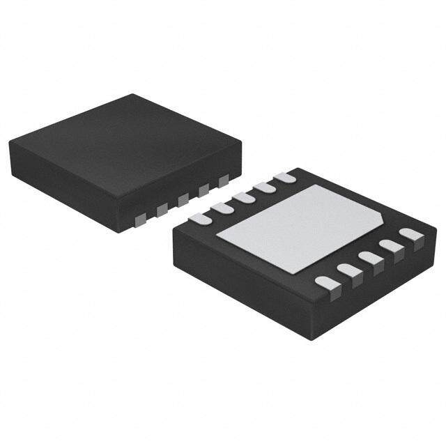
| 产品图片 |
|
| 产品型号 | LT3060EDC#TRMPBF |
| rohs | 无铅 / 符合限制有害物质指令(RoHS)规范要求 |
| 产品系列 | - |
| 产品目录页面 | |
| 供应商器件封装 | 8-DFN(2x2) |
| 其它名称 | LT3060EDC#TRMPBFTR |
| 包装 | 带卷 (TR) |
| 安装类型 | 表面贴装 |
| 封装/外壳 | 8-WFDFN 裸露焊盘 |
| 工作温度 | -40°C ~ 125°C |
| 标准包装 | 500 |
| 电压-跌落(典型值) | 0.3V @ 100mA |
| 电压-输入 | 1.6 V ~ 45 V |
| 电压-输出 | 0.6 V ~ 44.5 V |
| 电流-输出 | 100mA |
| 电流-限制(最小值) | 110mA |
| 稳压器拓扑 | 正,可调式 |
| 稳压器数 | 1 |


- 商务部:美国ITC正式对集成电路等产品启动337调查
- 曝三星4nm工艺存在良率问题 高通将骁龙8 Gen1或转产台积电
- 太阳诱电将投资9.5亿元在常州建新厂生产MLCC 预计2023年完工
- 英特尔发布欧洲新工厂建设计划 深化IDM 2.0 战略
- 台积电先进制程称霸业界 有大客户加持明年业绩稳了
- 达到5530亿美元!SIA预计今年全球半导体销售额将创下新高
- 英特尔拟将自动驾驶子公司Mobileye上市 估值或超500亿美元
- 三星加码芯片和SET,合并消费电子和移动部门,撤换高东真等 CEO
- 三星电子宣布重大人事变动 还合并消费电子和移动部门
- 海关总署:前11个月进口集成电路产品价值2.52万亿元 增长14.8%


PDF Datasheet 数据手册内容提取
LT3060 Series 45V V , Micropower, IN Low Noise, 100mA Low Dropout, Linear Regulator FeaTures DescripTion n Input Voltage Range: 1.6V to 45V The LT®3060 series are micropower, low dropout voltage n Output Current: 100mA (LDO) linear regulators that operate over a 1.6V to 45V n Quiescent Current: 40µA input supply range. The devices supply 100mA of output n Dropout Voltage: 300mV current with a typical dropout voltage of 300mV. A single n Low Noise: 30µV (10Hz to 100kHz) external capacitor provides programmable low noise RMS n Adjustable Output: V = 600mV reference performance and output soft-start functional- REF n Fixed Output Voltages: 1.2V, 1.5V, 1.8V, 2.5V, 3.3V, ity. The LT3060’s quiescent current is merely 40μA and 5V, 15V provides fast transient response with a minimum 2.2μF n Output Tolerance: ±2% Over Line, Load and output capacitor. In shutdown, quiescent current is less Temperature than 1μA and the reference soft-start capacitor is reset. n Single Capacitor Soft-Starts Reference and Lowers The LT3060 regulators optimize stability and transient Output Noise response with low ESR, ceramic output capacitors. n Shutdown Current: < 1µA The regulators do not require the addition of ESR as is n Reverse Battery Protection common with other regulators. n Current Limit Foldback Protection n Thermal Limit Protection Internal protection circuitry includes reverse-battery n 8-Lead 2mm × 2mm × 0.75mm DFN and 8-Lead protection, reverse-output protection, reverse-current ThinSOT™ Packages protection, current limit with foldback and thermal shutdown. The LT3060 series are available in fixed output applicaTions voltages of 1.2V, 1.5V, 1.8V, 2.5V, 3.3V, 5V and 15V, and as an adjustable voltage regulator with an output voltage range n Battery-Powered Systems from the 600mV reference to 44.5V. The LT3060 regulators n Automotive Power Supplies are offered in the thermally enhanced 8-lead TSOT-23 and n Industrial Power Supplies 8-lead (2mm × 2mm × 0.75mm) DFN packages. n Avionic Power Supplies L, LT, LTC, LTM, Linear Technology and the Linear logo are registered trademarks and n Portable Instruments ThinSOT is a trademark of Linear Technology Corporation. All other trademarks are the property of their respective owners. Typical applicaTion Dropout Voltage 350 2.5V Low Noise Regulator TJ = 25°C 300 IN OUT V2.O5UVT AT 100mA mV) 250 34VV5INV TO 1µF LT3060-2.5 C10FFnF 1300µµFVRMS NOISE LTAGE ( 200 O SHDN ADJ T V 150 U O GND REF/BYP P RO 100 D 10nF 50 3060 TA01 0 0 10 20 30 40 50 60 70 80 90 100 OUTPUT CURRENT (mA) 3060 TA02 3060fc 1 For more information www.linear.com/LT3060
LT3060 Series absoluTe MaxiMuM raTings (Note 1) IN Pin Voltage ........................................................±50V Output Short-Circuit Duration ..........................Indefinite OUT Pin Voltage .....................................................±50V Operating Junction Temperature (Notes 3, 5, 13) Input-to-Output Differential Voltage (Note 2) .........±50V E-, I-Grades .......................................–40°C to 125°C ADJ Pin Voltage .....................................................±50V MP-Grade ..........................................–55°C to 150°C SHDN Pin Voltage ..................................................±50V H-Grade .............................................–40°C to 150°C REF/BYP Pin Voltage .......................................–0.3V, 1V Storage Temperature Range ..................–65°C to 150°C Lead Temperature (TS8 Soldering, 10 sec) ...........300°C pin conFiguraTion TOP VIEW TOP VIEW REF/BYP 1 8 GND SHDN 1 8 REF/BYP ADJ 2 9 7 SHDN GND 2 7 ADJ OUT 3 GND 6 IN GND 3 6 OUT OUT 4 5 IN GND 4 5 IN DC PACKAGE TS8 PACKAGE 8-LEAD (2mm × 2mm) PLASTIC DFN 8-LEAD PLASTIC TSOT-23 TJMAX = 125°C, θJA = 48°C/W TO 60°C/W*, θJC = 20°C/W TJMAX = 150°C, θJA = 57°C/W TO 67°C/W*, θJC = 25°C/W EXPOSED PAD (PIN 9) IS GND, MUST BE SOLDERED TO PCB * SEE APPLICATIONS INFORMATION SECTION orDer inForMaTion LEAD FREE FINISH TAPE AND REEL PART MARKING* PACKAGE DESCRIPTION TEMPERATURE RANGE LT3060EDC#PBF LT3060EDC#TRPBF LDTD 8-Lead (2mm × 2mm) Plastic DFN –40°C to 125°C LT3060IDC#PBF LT3060IDC#TRPBF LDTD 8-Lead (2mm × 2mm) Plastic DFN –40°C to 125°C LT3060EDC-1.2#PBF LT3060EDC-1.2#TRPBF LFVT 8-Lead (2mm × 2mm) Plastic DFN –40°C to 125°C LT3060IDC-1.2#PBF LT3060IDC-1.2#TRPBF LFVT 8-Lead (2mm × 2mm) Plastic DFN –40°C to 125°C LT3060EDC-1.5#PBF LT3060EDC-1.5#TRPBF LFVV 8-Lead (2mm × 2mm) Plastic DFN –40°C to 125°C LT3060IDC-1.5#PBF LT3060IDC-1.5#TRPBF LFVV 8-Lead (2mm × 2mm) Plastic DFN –40°C to 125°C LT3060EDC-1.8#PBF LT3060EDC-1.8#TRPBF LFVW 8-Lead (2mm × 2mm) Plastic DFN –40°C to 125°C LT3060IDC-1.8#PBF LT3060IDC-1.8#TRPBF LFVW 8-Lead (2mm × 2mm) Plastic DFN –40°C to 125°C LT3060EDC-2.5#PBF LT3060EDC-2.5#TRPBF LFVX 8-Lead (2mm × 2mm) Plastic DFN –40°C to 125°C LT3060IDC-2.5#PBF LT3060IDC-2.5#TRPBF LFVX 8-Lead (2mm × 2mm) Plastic DFN –40°C to 125°C LT3060EDC-3.3#PBF LT3060EDC-3.3#TRPBF LFVY 8-Lead (2mm × 2mm) Plastic DFN –40°C to 125°C LT3060IDC-3.3#PBF LT3060IDC-3.3#TRPBF LFVY 8-Lead (2mm × 2mm) Plastic DFN –40°C to 125°C LT3060EDC-5#PBF LT3060EDC-5#TRPBF LFVZ 8-Lead (2mm × 2mm) Plastic DFN –40°C to 125°C LT3060IDC-5#PBF LT3060IDC-5#TRPBF LFVZ 8-Lead (2mm × 2mm) Plastic DFN –40°C to 125°C LT3060EDC-15#PBF LT3060EDC-15#TRPBF LGSK 8-Lead (2mm × 2mm) Plastic DFN –40°C to 125°C LT3060IDC-15#PBF LT3060IDC-15#TRPBF LGSK 8-Lead (2mm × 2mm) Plastic DFN –40°C to 125°C 3060fc 2 For more information www.linear.com/LT3060
LT3060 Series orDer inForMaTion LEAD FREE FINISH TAPE AND REEL PART MARKING* PACKAGE DESCRIPTION TEMPERATURE RANGE LT3060ETS8#PBF LT3060ETS8#TRPBF LTDTF 8-Lead Plastic ThinSOT –40°C to 125°C LT3060ITS8#PBF LT3060ITS8#TRPBF LTDTF 8-Lead Plastic ThinSOT –40°C to 125°C LT3060MPTS8#PBF LT3060MPTS8#TRPBF LTDTF 8-Lead Plastic ThinSOT –55°C to 150°C LT3060HTS8#PBF LT3060HTS8#TRPBF LTDTF 8-Lead Plastic ThinSOT –40°C to 150°C LT3060ETS8-1.2#PBF LT3060ETS8-1.2#TRPBF LTFWB 8-Lead Plastic ThinSOT –40°C to 125°C LT3060ITS8-1.2#PBF LT3060ITS8-1.2#TRPBF LTFWB 8-Lead Plastic ThinSOT –40°C to 125°C LT3060MPTS8-1.2#PBF LT3060MPTS8-1.2#TRPBF LTFWB 8-Lead Plastic ThinSOT –55°C to 150°C LT3060HTS8-1.2#PBF LT3060HTS8-1.2#TRPBF LTFWB 8-Lead Plastic ThinSOT –40°C to 150°C LT3060ETS8-1.5#PBF LT3060ETS8-1.5#TRPBF LTFWC 8-Lead Plastic ThinSOT –40°C to 125°C LT3060ITS8-1.5#PBF LT3060ITS8-1.5#TRPBF LTFWC 8-Lead Plastic ThinSOT –40°C to 125°C LT3060MPTS8-1.5#PBF LT3060MPTS8-1.5#TRPBF LTFWC 8-Lead Plastic ThinSOT –55°C to 150°C LT3060HTS8-1.5#PBF LT3060HTS8-1.5#TRPBF LTFWC 8-Lead Plastic ThinSOT –40°C to 150°C LT3060ETS8-1.8#PBF LT3060ETS8-1.8#TRPBF LTFWD 8-Lead Plastic ThinSOT –40°C to 125°C LT3060ITS8-1.8#PBF LT3060ITS8-1.8#TRPBF LTFWD 8-Lead Plastic ThinSOT –40°C to 125°C LT3060MPTS8-1.8#PBF LT3060MPTS8-1.8#TRPBF LTFWD 8-Lead Plastic ThinSOT –55°C to 150°C LT3060HTS8-1.8#PBF LT3060HTS8-1.8#TRPBF LTFWD 8-Lead Plastic ThinSOT –40°C to 150°C LT3060ETS8-2.5#PBF LT3060ETS8-2.5#TRPBF LTFWF 8-Lead Plastic ThinSOT –40°C to 125°C LT3060ITS8-2.5#PBF LT3060ITS8-2.5#TRPBF LTFWF 8-Lead Plastic ThinSOT –40°C to 125°C LT3060MPTS8-2.5#PBF LT3060MPTS8-2.5#TRPBF LTFWF 8-Lead Plastic ThinSOT –55°C to 150°C LT3060HTS8-2.5#PBF LT3060HTS8-2.5#TRPBF LTFWF 8-Lead Plastic ThinSOT –40°C to 150°C LT3060ETS8-3.3#PBF LT3060ETS8-3.3#TRPBF LTFWG 8-Lead Plastic ThinSOT –40°C to 125°C LT3060ITS8-3.3#PBF LT3060ITS8-3.3#TRPBF LTFWG 8-Lead Plastic ThinSOT –40°C to 125°C LT3060MPTS8-3.3#PBF LT3060MPTS8-3.3#TRPBF LTFWG 8-Lead Plastic ThinSOT –55°C to 150°C LT3060HTS8-3.3#PBF LT3060HTS8-3.3#TRPBF LTFWG 8-Lead Plastic ThinSOT –40°C to 150°C LT3060ETS8-5#PBF LT3060ETS8-5#TRPBF LTFWH 8-Lead Plastic ThinSOT –40°C to 125°C LT3060ITS8-5#PBF LT3060ITS8-5#TRPBF LTFWH 8-Lead Plastic ThinSOT –40°C to 125°C LT3060MPTS8-5#PBF LT3060MPTS8-5#TRPBF LTFWH 8-Lead Plastic ThinSOT –55°C to 150°C LT3060HTS8-5#PBF LT3060HTS8-5#TRPBF LTFWH 8-Lead Plastic ThinSOT –40°C to 150°C LT3060ETS8-15#PBF LT3060ETS8-15#TRPBF LTGSM 8-Lead Plastic ThinSOT –40°C to 125°C LT3060ITS8-15#PBF LT3060ITS8-15#TRPBF LTGSM 8-Lead Plastic ThinSOT –40°C to 125°C LT3060MPTS8-15#PBF LT3060MPTS8-15#TRPBF LTGSM 8-Lead Plastic ThinSOT –55°C to 150°C LT3060HTS8-15#PBF LT3060HTS8-15#TRPBF LTGSM 8-Lead Plastic ThinSOT –40°C to 150°C Consult LTC Marketing for parts specified with wider operating temperature ranges. *The temperature grade is identified by a label on the shipping container. Consult LTC Marketing for information on nonstandard lead based finish parts. For more information on lead free part marking, go to: http://www.linear.com/leadfree/ For more information on tape and reel specifications, go to: http://www.linear.com/tapeandreel/ 3060fc 3 For more information www.linear.com/LT3060
LT3060 Series elecTrical characTerisTics The l denotes the specifications which apply over the full operating temperature range, otherwise specifications are at T = 25°C. (Note 3) A PARAMETER CONDITIONS MIN TYP MAX UNITS Minimum Input Voltage I = 100mA l 1.6 2.1 V LOAD (Notes 4, 12) Regulated Output Voltage LT3060-1.2: VIN = 2.1V, ILOAD = 1mA 1.188 1.2 1.212 V (Note 5) 2.1V < VIN < 45V, 1mA < ILOAD < 100mA (E-, I-Grades) l 1.176 1.2 1.224 V 2.1V < VIN < 45V, 1mA < ILOAD < 100mA (MP-, H-Grades) l 1.170 1.2 1.224 V LT3060-1.5: VIN = 2.1V, ILOAD = 1mA 1.485 1.5 1.515 V 2.1V < VIN < 45V, 1mA < ILOAD < 100mA (E-, I-Grades) l 1.470 1.5 1.530 V 2.1V < VIN < 45V, 1mA < ILOAD < 100mA (MP-, H-Grades) l 1.463 1.5 1.530 V LT3060-1.8: VIN = 2.35V, ILOAD = 1mA 1.782 1.8 1.818 V 2.35V < VIN < 45V, 1mA < ILOAD < 100mA (E-, I-Grades) l 1.764 1.8 1.836 V 2.35V < VIN < 45V, 1mA < ILOAD < 100mA (MP-, H-Grades) l 1.755 1.8 1.836 V LT3060-2.5: VIN = 3.05V, ILOAD = 1mA 2.475 2.5 2.525 V 3.05V < VIN < 45V, 1mA < ILOAD < 100mA (E-, I-Grades) l 2.450 2.5 2.550 V 3.05V < VIN < 45V, 1mA < ILOAD < 100mA (MP-, H-Grades) l 2.438 2.5 2.550 V LT3060-3.3: VIN = 3.85V, ILOAD = 1mA 3.267 3.3 3.333 V 3.85V < VIN < 45V, 1mA < ILOAD < 100mA (E-, I-Grades) l 3.234 3.3 3.366 V 3.85V < VIN < 45V, 1mA < ILOAD < 100mA (MP-, H-Grades) l 3.218 3.3 3.366 V LT3060-5: VIN = 5.55V, ILOAD = 1mA 4.950 5 5.050 V 5.55V < VIN < 45V, 1mA < ILOAD < 100mA (E-, I-Grades) l 4.900 5 5.100 V 5.55V < VIN < 45V, 1mA < ILOAD < 100mA (MP-, H-Grades) l 4.875 5 5.100 V LT3060-15: VIN = 15.55V, ILOAD = 1mA 14.85 15 15.15 V 15.55V < VIN < 45V, 1mA < ILOAD < 100mA (E-, I-Grades) l 14.70 15 15.30 V 15.55V < VIN < 45V, 1mA < ILOAD < 100mA (MP-, H-Grades) l 14.63 15 15.30 V ADJ Pin Voltage LT3060: V = 2.1V, I = 1mA 594 600 606 mV IN LOAD (Notes 4, 5) 2.1V < V < 45V, 1mA < I < 100mA (E-, I-Grades) l 588 600 612 mV IN LOAD 2.1V < V < 45V, 1mA < I < 100mA (MP-, H-Grades) l 585 600 612 mV IN LOAD Line Regulation LT3060-1.2: ΔVIN = 2.1V to 45V, ILOAD = 1mA (E-, I-Grades) l 0.9 3.5 mV ΔVIN = 2.1V to 45V, ILOAD = 1mA (MP-, H-Grades) l 7 LT3060-1.5: ΔVIN = 2.1V to 45V, ILOAD = 1mA (E-, I-Grades) l 1 4.2 mV ΔVIN = 2.1V to 45V, ILOAD = 1mA (MP-, H-Grades) l 8 LT3060-1.8: ΔVIN = 2.35V to 45V, ILOAD = 1mA (E-, I-Grades) l 1.1 4.5 mV ΔVIN = 2.35V to 45V, ILOAD = 1mA (MP-, H-Grades) l 12 LT3060-2.5: ΔVIN = 3.05V to 45V, ILOAD = 1mA (E-, I-Grades) l 1.2 5.4 mV ΔVIN = 3.05V to 45V, ILOAD = 1mA (MP-, H-Grades) l 15 LT3060-3.3: ΔVIN = 3.85V to 45V, ILOAD = 1mA (E-, I-Grades) l 1.3 7 mV ΔVIN = 3.85V to 45V, ILOAD = 1mA (MP-, H-Grades) l 19 LT3060-5: ΔVIN = 5.55V to 45V, ILOAD = 1mA (E-, I-Grades) l 1.5 8.5 mV ΔVIN = 5.55V to 45V, ILOAD = 1mA (MP-, H-Grades) l 25 LT3060-15: ΔVIN = 15.55V to 45V, ILOAD = 1mA (E-, I-Grades) l 2.2 22 mV ΔVIN = 15.55V to 45V, ILOAD = 1mA (MP-, H-Grades) l 55 LT3060: ΔVIN = 2.1V to 45V, ILOAD = 1mA (E-, I-Grades) l 0.6 3.5 mV (Note 4) ΔVIN = 2.1V to 45V, ILOAD = 1mA (MP-, H-Grades) l 4 3060fc 4 For more information www.linear.com/LT3060
LT3060 Series elecTrical characTerisTics The l denotes the specifications which apply over the full operating temperature range, otherwise specifications are at T = 25°C. (Note 3) A PARAMETER CONDITIONS MIN TYP MAX UNITS Load Regulation LT3060-1.2: V = 2.1V, I = 1mA to 100mA (E-, I-Grades) l 2.4 10 mV IN LOAD (Note 15) V = 2.1V, I = 1mA to 100mA (MP-, H-Grades) l 18 mV IN LOAD LT3060-1.5: V = 2.1V, I = 1mA to 100mA (E-, I-Grades) l 2.5 12 mV IN LOAD V = 2.1V, I = 1mA to 100mA (MP-, H-Grades) l 22 mV IN LOAD LT3060-1.8: V = 2.35V, I = 1mA to 100mA (E-, I-Grades) l 2.6 14 mV IN LOAD V = 2.35V, I = 1mA to 100mA (MP-, H-Grades) l 27 mV IN LOAD LT3060-2.5: V = 3.05V, I = 1mA to 100mA (E-, I-Grades) l 2.8 19 mV IN LOAD V = 3.05V, I = 1mA to 100mA (MP-, H-Grades) l 37 mV IN LOAD LT3060-3.3: V = 3.85V, I = 1mA to 100mA (E-, I-Grades) l 3.1 24 mV IN LOAD V = 3.85V, I = 1mA to 100mA (MP-, H-Grades) l 49 mV IN LOAD LT3060-5: V = 5.55V, I = 1mA to 100mA (E-, I-Grades) l 3.7 35 mV IN LOAD V = 5.55V, I = 1mA to 100mA (MP-, H-Grades) l 75 mV IN LOAD LT3060-15: V = 15.55V, I = 1mA to 100mA (E-, I-Grades) l 7 100 mV IN LOAD V = 15.55V, I = 1mA to 100mA (MP-, H-Grades) l 225 mV IN LOAD LT3060: V = 2.1V, I = 1mA to 100mA (E-, I-Grades) l 0.2 4 mV IN LOAD (Note 4) V = 2.1V, I = 1mA to 100mA (MP-, H-Grades) l 9 mV IN LOAD Dropout Voltage I = 1mA 75 110 mV LOAD V = V I = 1mA l 180 mV IN OUT(NOMINAL) LOAD (Notes 6, 7) I = 10mA 150 200 mV LOAD I = 10mA l 300 mV LOAD I = 50mA (Note 14) 240 280 mV LOAD I = 50mA (Note 14) l 410 mV LOAD I = 100mA (Note 14) 300 350 mV LOAD I = 100mA (Note 14) l 510 mV LOAD GND Pin Current I = 0µA l 40 80 µA LOAD V = V + I = 1mA l 60 100 µA IN OUT(NOMINAL) LOAD 0.55V I = 10mA l 160 350 µA LOAD (Notes 6, 8) ILOAD = 50mA l 0.8 1.8 mA I = 100mA l 2 4 mA LOAD Quiescent Current in V = 45V, V = 0V 0.3 1 µA IN SHDN Shutdown ADJ Pin Bias Current V = 2.1V l 15 60 nA IN (Note 9) Output Voltage Noise C = 10µF, I = 100mA, C = 0.01µF 30 µV OUT LOAD BYP RMS V = 600mV, BW = 10Hz to 100kHz OUT Shutdown Threshold V = Off to On l 0.8 1.5 V OUT V = On to Off l 0.3 0.7 V OUT SHDN Pin Current V = 0V l 1 µA SHDN (Note 10) V = 45V l 0.9 3 µA SHDN Ripple Rejection LT3060-1.2: V = 2.7V (Avg) 64 79 dB IN V = 0.5V , RIPPLE P-P LT3060-1.5: V = 3V (Avg) 62 77 dB f = 120Hz, IN RIPPLE ILOAD = 100mA LT3060-1.8: VIN = 3.3V (Avg) 60 75 dB LT3060-2.5: V = 4V (Avg) 58 73 dB IN LT3060-3.3: V = 4.8V (Avg) 55 70 dB IN LT3060-5: V = 6.5V (Avg) 52 67 dB IN LT3060-15: V = 16.5V (Avg) 45 60 dB IN LT3060: V = 2.1V (Avg) (Note 4) 70 85 dB IN Current Limit V = 7V, V = 0 200 mA IN OUT VIN = VOUT(NOMINAL) + 1V (Notes 6, 12), ΔVOUT = –5% l 110 mA 3060fc 5 For more information www.linear.com/LT3060
LT3060 Series elecTrical characTerisTics The l denotes the specifications which apply over the full operating temperature range, otherwise specifications are at T = 25°C. (Note 3) A PARAMETER CONDITIONS MIN TYP MAX UNITS Input Reverse Leakage V = –45V, V = 0 l 300 µA IN OUT Current Reverse Output Current LT3060-1.2: V = 1.2V, V = 0V 5 10 µA OUT IN (Note 11) LT3060-1.5: V = 1.5V, V = 0V 5 10 µA OUT IN LT3060-1.8: V = 1.8V, V = 0V 5 10 µA OUT IN LT3060-2.5: V = 2.5V, V = 0V 5 10 µA OUT IN LT3060-3.3: V = 3.3V, V = 0V 5 10 µA OUT IN LT3060-5: V = 5V, V = 0V 5 10 µA OUT IN LT3060-15: V = 15V, V = 0V 5 10 µA OUT IN LT3060: V = 1.2V, V = 0V 0.2 10 µA OUT IN Note 1: Stresses beyond those listed under Absolute Maximum Ratings Note 7: Dropout voltage is the minimum input-to-output voltage may cause permanent damage to the device. Exposure to any Absolute differential needed to maintain regulation at a specified output current. Maximum Rating condition for extended periods may affect device In dropout, the output voltage equals: (V – V ). For the IN DROPOUT reliability and lifetime. LT3060, LT3060-1.2, LT3060-1.5 and LT3060-1.8, dropout is limited Note 2: Absolute maximum input-to-output differential voltage is not by the minimum input specification under some output voltages and achievable with all combinations of rated IN pin and OUT pin voltages. load conditions. See the Minimum Input Voltage curve in the Typical With the IN pin at 50V, the OUT pin may not be pulled below 0V. The total Performance Characteristics section. measured voltage from IN to OUT must not exceed ±50V. If OUT is above Note 8: GND pin current is tested with V = V + 0.55V and a IN OUT(NOMINAL) ground, do not actively pull OUT above IN by more than 40V. current source load. GND pin current will increase in dropout. See GND pin Note 3: The LT3060 regulators are tested and specified under pulse load current curves in the Typical Performance Characteristics section. conditions such that TJ ≅ TA. The LT3060E regulators are 100% tested Note 9: ADJ pin bias current flows out of the ADJ pin. at T = 25°C. Performance at –40°C to 125°C is assured by design, A Note 10: SHDN pin current flows into the SHDN pin. characterization and correlation with statistical process controls. The Note 11: Reverse output current is tested with the IN pin grounded and the LT3060I regulators are guaranteed over the full –40°C to 125°C operating OUT pin forced to the rated output voltage. This current flows into the OUT junction temperature range. The LT3060MP regulators are 100% tested over the –55°C to 150°C operating junction temperature range. The pin and out of the GND pin. LT3060H regulators are 100% tested at the 150°C operating junction Note 12: To satisfy requirements for minimum input voltage, current temperature. High junction temperatures degrade operating lifetimes. limit is tested at VIN = VOUT(NOMINAL) + 1V or VIN = 2.1V, whichever is Operating lifetime is derated at junction temperatures greater than 125°C. greater. Note 4: The LT3060 adjustable version is tested and specified for these Note 13: This IC includes overtemperature protection that protects the conditions with the ADJ connected to the OUT pin. device during momentary overload conditions. Junction temperature Note 5: Maximum junction temperature limits operating conditions. The will exceed 125°C (LT3060E, LT3060I) or 150°C (LT3060MP, LT3060H) regulated output voltage specification does not apply for all possible when overtemperature circuitry is active. Continuous operation above the combinations of input voltage and output current. Limit the output current specified maximum junction temperature may impair device reliability. range if operating at the maximum input-to-output voltage differential. Note 14: The dropout voltage specification is guaranteed for the DFN Limit the input-to-output voltage differential if operating at maximum package. The dropout voltage specification for high output currents cannot output current. Current limit foldback will limit the maximum output be guaranteed for the TS8 package due to production test limitations. current as a function of input-to-output voltage. See Current Limit vs Note 15: The load regulation specification is guaranteed for the fixed V – V in the Typical Performance Characteristics section. IN OUT voltage options in the DFN package. The load regulation specification Note 6: To satisfy minimum input voltage requirements, the LT3060 cannot be guaranteed for the fixed voltage options in the TS8 package due adjustable version is tested and specified for these conditions with an to production test limitations. The TS8 packages are tested similarly to the external resistor divider (bottom 115k, top 365k) for an output voltage of LT3060 adjustable version with the ADJ connected to the OUT pin. 2.5V. The external resistor divider adds 5µA of DC load on the output. This external current is not factored into GND pin current. 3060fc 6 For more information www.linear.com/LT3060
LT3060 Series Typical perForMance characTerisTics T = 25°C, unless otherwise noted. A Typical Dropout Voltage Guaranteed Dropout Voltage Dropout Voltage 550 550 550 = TEST POINTS 500 V) 500 500 m 450 E ( 450 450 IL = 100mA LTAGE (mV) 343500000 TJ = 125°C OUT VOLTAG 433050000 TJ ≤ 150°C LTAGE (mV) 433050000 IL = 50mA OUT VO 225000 TJ = 25°C D DROP 225000 TJ ≤ 25°C OUT VO 225000 IL = 10mA OP EE OP DR 150 NT 150 DR 150 IL = 1mA A 100 R 100 100 A U 50 G 50 50 0 0 0 0 10 20 30 40 50 60 70 80 90 100 0 10 20 30 40 50 60 70 80 90 100 –75–50–25 0 25 50 75 100125150175 OUTPUT CURRENT (mA) OUTPUT CURRENT (mA) TEMPERATURE (°C) 3060 G01 3060 G02 3060 G03 Quiescent Current LT3060-1.2 Output Voltage LT3060-1.5 Output Voltage 80 1.224 1.530 VIN = 6V, VSHDN = VIN 1.220 IL = 1mA 1.525 IL = 1mA 70 RL = ∞ (120k FOR LT3060) IL = 0 (5µA FOR LT3060) 1.216 1.520 A) 60 1.212 1.515 RENT (µ 50 LT3060-1.2/-1.5/-1.8/-2.5/-3.3/-5 AGE (V)11..220048 AGE (V)11..550150 NT CUR 40 LT3060 UT VOLT11..210906 UT VOLT11..540905 UIESCE 3200 OUTP11..119828 OUTP11..449805 Q 1.184 1.480 10 VSHDN = 0V 1.180 1.475 0 1.176 1.470 –75–50–25 0 25 50 75 100125150175 –75–50–25 0 25 50 75 100125150175 –75–50–25 0 25 50 75 100125150175 TEMPERATURE (°C) TEMPERATURE (°C) TEMPERATURE (°C) 3060 G04 3060 G05 3060 G06 LT3060-1.8 Output Voltage LT3060-2.5 Output Voltage LT3060-3.3 Output Voltage 1.836 2.55 3.366 1.830 IL = 1mA IL = 1mA 3.355 IL = 1mA 2.54 1.824 3.344 2.53 1.818 3.333 AGE (V)11..880162 AGE (V) 22..5512 AGE (V)33..331212 OLT1.800 OLT 2.50 OLT3.300 V V V UT 1.794 UT 2.49 UT 3.289 P P P OUT11..778882 OUT 2.48 OUT33..227687 2.47 1.776 3.256 1.770 2.46 3.245 1.764 2.45 3.234 –75–50–25 0 25 50 75 100125150175 –75–50–25 0 25 50 75 100125150175 –75–50–25 0 25 50 75 100125150175 TEMPERATURE (°C) TEMPERATURE (°C) TEMPERATURE (°C) 3060 G07 3060 G08 3060 G09 3060fc 7 For more information www.linear.com/LT3060
LT3060 Series Typical perForMance characTerisTics T = 25°C, unless otherwise noted. A LT3060-5 Output Voltage LT3060-15 Output Voltage LT3060 ADJ Pin Voltage 5.10 15.30 0.612 5.08 IL = 1mA 15.25 IL = 1mA 0.610 VILI N= =1 m2.A1V 15.20 0.608 5.06 15.15 0.606 OLTAGE (V) 555...000024 OLTAGE (V)111555...001050 OLTAGE (V)000...666000024 V V V OUTPUT 44..9986 OUTPUT 1144..9950 ADJ PIN 00..559986 14.85 0.594 4.94 14.80 0.592 4.92 14.75 0.590 4.90 14.70 0.588 –75–50–25 0 25 50 75 100125150175 –75–50–25 0 25 50 75 100125150175 –75–50–25 0 25 50 75 100125150175 TEMPERATURE (°C) TEMPERATURE (°C) TEMPERATURE (°C) 3060 G10 3060 G10a 3060 G11 LT3060-1.2 Quiescent Current LT3060-1.5 Quiescent Current LT3060-1.8 Quiescent Current 200 200 200 TJ = 25°C TJ = 25°C TJ = 25°C 175 RL = ∞ 175 RL = ∞ 175 RL = ∞ VOUT = 1.2V VOUT = 1.5V VOUT = 1.8V A) 150 A) 150 A) 150 µ µ µ T ( T ( T ( EN 125 EN 125 EN 125 R R R R R R CU 100 CU 100 CU 100 T T T N N N CE 75 CE 75 CE 75 S S S UIE 50 VSHDN = VIN UIE 50 VSHDN = VIN UIE 50 VSHDN = VIN Q Q Q 25 25 25 VSHDN = 0V VSHDN = 0V VSHDN = 0V 0 0 0 0 1 2 3 4 5 6 7 8 9 10 0 1 2 3 4 5 6 7 8 9 10 0 1 2 3 4 5 6 7 8 9 10 INPUT VOLTAGE (V) INPUT VOLTAGE (V) INPUT VOLTAGE (V) 3060 G12 3060 G13 3060 G14 LT3060-2.5 Quiescent Current LT3060-3.3 Quiescent Current LT3060-5 Quiescent Current 200 200 200 TJ = 25°C TJ = 25°C TJ = 25°C 175 RL = ∞ 175 RL = ∞ 175 RL = ∞ VOUT = 2.5V VOUT = 3.3V VOUT = 5V RENT (µA) 112550 RENT (µA) 112550 RENT (µA) 112550 R R R CU 100 CU 100 CU 100 NT NT NT CE 75 CE 75 CE 75 S S S QUIE 50 VSHDN = VIN QUIE 50 VSHDN = VIN QUIE 50 VSHDN = VIN 25 25 25 VSHDN = 0V VSHDN = 0V VSHDN = 0V 0 0 0 0 1 2 3 4 5 6 7 8 9 10 0 1 2 3 4 5 6 7 8 9 10 0 1 2 3 4 5 6 7 8 9 10 INPUT VOLTAGE (V) INPUT VOLTAGE (V) INPUT VOLTAGE (V) 3060 G15 3060 G16 3060 G17 3060fc 8 For more information www.linear.com/LT3060
LT3060 Series Typical perForMance characTerisTics T = 25°C, unless otherwise noted. A LT3060-15 Quiescent Current LT3060 Quiescent Current LT3060-1.2 GND Pin Current 200 80 2.50 TJ = 25°C TJ = 25°C TJ = 25°C 175 RL = ∞ 70 RL = 120k 2.25 *FOR VOUT = 1.2V VOUT = 15V VOUT = 0.6V 2.00 VSHDN = VIN µA) 150 µA) 60 A) CENT CURRENT ( 11027055 VSHDN = VIN CENT CURRENT ( 543000 VSHDN = VIN PIN CURRENT (m 1111....75205050 IRLL = = 1 1020ΩmA* RL = 24Ω QUIES 5205 QUIES 2100 GND 000...752505 IRLL = = 1 1m.2Ak* IIRLLL == = 51 1002mm0AAΩ** VSHDN = 0V VSHDN = 0 0 0 0 0 5 10 15 20 25 30 35 40 45 0 5 10 15 20 25 30 35 40 45 0 1 2 3 4 5 6 7 8 9 10 INPUT VOLTAGE (V) INPUT VOLTAGE (V) INPUT VOLTAGE (V) 3060 G17a 3060 G19 3060 G18 LT3060-1.5 GND Pin Current LT3060-1.8 GND Pin Current LT3060-2.5 GND Pin Current 2.50 2.50 2.50 TJ = 25°C TJ = 25°C TJ = 25°C 2.25 *FOR VOUT = 1.5V 2.25 *FOR VOUT = 1.8V 2.25 *FOR VOUT = 2.5V 2.00 VSHDN = VIN 2.00 VSHDN = VIN 2.00 VSHDN = VIN NT (mA) 11..7550 IRLL = = 1 1050ΩmA* NT (mA) 11..7550 IRLL = = 1 1080ΩmA* NT (mA) 11..7550 IRLL = = 1 2050ΩmA* RE RE RE UR 1.25 UR 1.25 UR 1.25 C C C D PIN 10..0705 IRLL = = 5 300mΩA* D PIN 10..0705 IRLL = = 5 306mΩA* D PIN 10..0705 IRLL = = 5 500mΩA* N N N G G G 00..5205 IRLL = = 1 1m.5Ak* IRLL = = 1 105m0AΩ* 00..5205 IRLL = = 1 1m.8Ak* IRLL = = 1 108m0AΩ* 00..5205 IRLL = = 1 2m.5Ak* IRLL = = 1 205m0AΩ* 0 0 0 0 1 2 3 4 5 6 7 8 9 10 0 1 2 3 4 5 6 7 8 9 10 0 1 2 3 4 5 6 7 8 9 10 INPUT VOLTAGE (V) INPUT VOLTAGE (V) INPUT VOLTAGE (V) 3060 G20 3060 G21 3060 G22 LT3060-3.3 GND Pin Current LT3060-5 GND Pin Current LT3060-15 GND Pin Current 2.50 2.50 2.50 22..2050 *FOR VVSOHTUDJT N == = 23 5V.3°ICVN 22..2050 *FORVS VHTODJU N=T = 2= 5V 5°ICVN A) 22..0205 IRLL = = 1 10500mΩA* *FORV VSOHTUDJT N= = =2 15V5°ICVN A) A) m GND PIN CURRENT (m 1111000.......75207525050505 IRLL IR=L =L =1 =3 01 303mΩm.3AAk** IIRRLLLL == == 15 360036mm0ΩAAΩ** GND PIN CURRENT (m 1111000.......75207525050505 IRLL = IR= L1 L 5=m =k 1 A50*00ΩmA*IIRRLLLL == == 15 510000mm00AAΩΩ** QUIESCENT CURRENT ( 1111000.......52707520550505 IRLL = IR= L5 L 3=0 =0 m1 01mAΩ5*Ak* IRLL = = 1 10.m5kA* 0 0 0 0 1 2 3 4 5 6 7 8 9 10 0 1 2 3 4 5 6 7 8 9 10 0 5 10 15 20 25 30 35 40 45 INPUT VOLTAGE (V) INPUT VOLTAGE (V) INPUT VOLTAGE (V) 3060 G23 3060 G24 3060 G24a 3060fc 9 For more information www.linear.com/LT3060
LT3060 Series Typical perForMance characTerisTics T = 25°C, unless otherwise noted. A LT3060 GND Pin Current GND Pin Current vs I SHDN Pin Threshold LOAD 2.50 4.0 1.5 TJ = 25°C VIN = VOUT(NOMINAL) + 1V 1.4 2.25 *FOR VOUT = 0.6V 3.5 1.3 2.00 VSHDN = VIN 1.2 NT (mA) 11..7550 IRLL = = 1 60Ω0mA* NT (mA) 32..05 HOLD (V) 011...901 CURRE 1.25 CURRE 2.0 THRES 00..78 OFF TO ON D PIN 10..0705 IRLL = = 5 102mΩA* D PIN 1.5 N PIN 00..65 ON TO OFF GN GN 1.0 HD 0.4 00..5205 IRLL = = 1 6m0A0Ω* IRLL = = 1 600mΩA* 0.5 S 00..23 0.1 0 0 0 0 1 2 3 4 5 6 7 8 9 10 0 10 20 30 40 50 60 70 80 90 100 –75–50–25 0 25 50 75 100125150175 INPUT VOLTAGE (V) OUTPUT CURRENT (mA) TEMPERATURE (°C) 3060 G25 3060 G26 3060 G27 SHDN Pin Input Current SHDN Pin Input Current ADJ Pin Bias Current 2.0 2.0 50 VSHDN = 45V 1.8 1.8 40 RRENT (µA) 111...462 RRENT (µA) 111...462 RENT (nA) 231000 U U R C C U N INPUT 10..08 N INPUT 10..08 N BIAS C –100 PI 0.6 PI 0.6 PI –20 N N J D D D H 0.4 H 0.4 A –30 S S 0.2 0.2 –40 0 0 –50 0 5 10 15 20 25 30 35 40 45 –75–50–25 0 25 50 75 100125150175 –75–50–25 0 25 50 75 100125150175 SHDN PIN VOLTAGE (V) TEMPERATURE (°C) TEMPERATURE (°C) 3060 G28 3060 G29 3060 G30 Current Limit vs V –V Current Limit vs Temperature LT3060 Reverse Output Current IN OUT 250 250 2.0 225 TJ = 125°C ∆VOUT = –5% 225 1.8 VTJIN = = 2 05V°C 200 TJ = 25°C 200 mA) 1.6 CURRENT FLOWS MIT (mA) 115705 TJ = –50°C MIT (mA) 1175504321----PPPPHHHHAAAASSSSEEEE CURRENT ( 11..42 IVNOTUOT O= UVTA DPJIN CURRENT LI 11207505 CURRENT LI 112075056-PHASE RSE OUTPUT 100...086 ADJ E 50 50 V 0.4 E R 25 25 VIN = 7V 0.2 VOUT = 0V OUT 0 0 0 0 5 10 15 20 25 30 35 40 45 –75–50–25 0 25 50 75 100125150175 0 5 10 15 20 25 30 35 40 45 INPUT/OUTPUT DIFFERENTIAL (V) TEMPERATURE (°C) OUTPUT VOLTAGE (V) 3060 G31 3060 G32 3060 G33 3060fc 10 For more information www.linear.com/LT3060
VOUT = 0.6V, COUT = 2.2µF VOUT = 3.3V VOUT = 2.5V VOUT = 1.8V LT3060 Series Typical perForMance characTerisTics T = 25°C, unless otherwise noted. A LT3060-1.2/-1.5/-1.8/-2.5/-3.3/-5 /-15 Reverse Output Current Reverse Output Current Input Ripple Rejection 350 50 100 TJ = 25°C LT3060-1.2 VIN = 0V, VOUT = VADJ = 1.2V (LT3060) µA) 300 VIN = 0V LT3060-1.5 µA) 4405 VVOOUUTT == 11..25VV ((LLTT33006600--11..25)) 8900 VOUT = 0.6V PUT CURRENT ( 225000 LT3060L-T33.306L0T-320.650-1.8 PUT CURRENT ( 332505 VVVVVOOOOOUUUUUTTTTT ===== 12351...V5853V VVV (((((LLLLLTTTTT33333000006666600000-----12351...)5853)))) EJECTION (dB) 675000 VOUT = 5V COUT = 10µF REVERSE OUT 11505000 LT3L0T6300-6105-5 REVERSE OUT 211005 O-1U.8T/ 2(L.5T/3-036.30/--15./2-1/-A51D). 5J/ (LT3060) RIPPLE R 432000 CILR =E F1/B0Y0Pm =A CFF = 0 5 10 VIN = VOUT(NOMINAL) + 1.5V + OUT (LT3060) 50mVRMS RIPPLE COUT = 2.2µF 0 0 0 0 5 10 15 20 25 30 35 40 45 –75–50–25 0 25 50 75 100125150175 10 100 1k 10k 100k 1M 10M OUTPUT VOLTAGE (V) TEMPERATURE (°C) FREQUENCY (Hz) 3060 G34 3060 G35 3060 G36 LT3060-5 Input Ripple Rejection LT3060-15 Input Ripple Rejection Ripple Rejection vs Temperature 100 100 100 90 CREF/BYP = CFF = 10nF 90 CREF/BYP = CFF = 10nF 90 CREF/BYP = 10nF 80 CREF/BYP = 10nF, CFF = 0 80 CREF/BYP = 10nF, CFF = 0 80 CREF/BYP = 0 dB) 70 dB) 70 dB) 70 N ( N ( N ( O 60 O 60 O 60 TI TI TI C C C EJE 50 EJE 50 EJE 50 E R 40 E R 40 E R 40 L L L PP 30 PP 30 PP 30 RI 20 IL = 100mA RI 20 IL = 100mA RI 20 VOUT = 5V CREF/BYP = CFF = 0 VOUT = 15V CREF/BYP = CFF = 0 IL = 100mA 10 COUT = 10µF 10 COUT = 10µF 10 VOUT = 0.6V VIN = 6V + 50mVRMS RIPPLE VIN = 16V + 50mVRMS RIPPLE VIN = 2.6V + 0.5VP-P RIPPLE AT f = 120Hz 0 0 0 10 100 1k 10k 100k 1M 10M 10 100 1k 10k 100k 1M 10M –75–50–25 0 25 50 75 100125150175 FREQUENCY (Hz) FREQUENCY (Hz) TEMPERATURE (°C) 3060 G37 3060 G37a 3060 G38 Minimum Input Voltage Load Regulation Load Regulation 2.2 5 0 LT3060-2.5 2.0 –5 0 V) 1.8 –10 OLTAGE ( 11..46 IL = 50mA IL = 100mA ON (mV) –5 ON (mV) ––1250 LT3060-5 NIMUM INPUT V 1100....2086 LOAD REGULATI ––1105 LLLLTTTT3333000066660000----5321...358 LOAD REGULATI –––233505 LT3060-15 MI 0.4 –20 LT3060-1.5 –40 0.2 LT3060-1.2 –45 VIN = VOUT(NOMINAL) + 0.55V VSHDN = VIN LT3060 ∆IL = 1mA TO 100mA 0 –25 –50 –75–50–25 0 25 50 75 100125150175 –75–50–25 0 25 50 75 100125150175 –75–50–25 0 25 50 75 100125150175 TEMPERATURE (°C) TEMPERATURE (°C) 3060 G40 TEMPERATURE (°C) 3060 G40a 3060 G39 VIN = VOUT(NOMINAL) + 0.55V (LT3060-1.8/-2.5/-3.3/-5) VIN = 2.1V (LT3060/-1.2/-1.5) ∆IL = 1mA TO 100mA 3060fc 11 For more information www.linear.com/LT3060
LT3060 Series Typical perForMance characTerisTics T = 25°C, unless otherwise noted. A Output Noise Spectral Density Output Noise Spectral Density Output Noise Spectral Density CREF/BYP = 0, CFF = 0 vs CREF/BYP, CFF = 0 vs CFF, CREF/BYP = 10nF 100 10 10 OUTPUT NOISE SPECTRAL DENSITY (µV/√Hz) 0.001.1011 CILO =U T1 0=0 VVVV1m0OOOOAµUUUUFTTTT ==== 15325V..35VVV VVVVOOOOUUUUTTTT ==== 1110....8526VVVV OUTPUT NOISE SPECTRAL DENSITY (µV/√Hz) 0.00.111 VVCILOOO =UUUC TTTR1 ==0E=F 0 05/1mB.V06YAµVPF = 10nF CREF/BCYRPE F=/ B1YnPF = 100pF OUTPUT NOISE SPECTRAL DENSITY (µV/√Hz) 0.00.111 CVCILFOO F=UU =TT1 01==00 51mnV0FAµF CFF = 1nF CFF = 10C0FpF F= 0 10 100 1k 10k 100k 10 100 1k 10k 100k 10 100 1k 10k 100k FREQUENCY (Hz) 3060 G41 FREQUENCY (Hz) 3060 G42 FREQUENCY (Hz) 3060 G43 RMS Output Noise vs Load Current RMS Output Noise vs Load Current RMS Output Noise vs Load Current vs C , C = 0 C = 10nF, C = 0 C = 10nF, C = 0 REF/BYP FF REF/BYP FF REF/BYP FF 110 170 350 OUTPUT NOISE VOLTAGE (µV)RMS 143210987650000000000 VCCCOORRUUEETTFF //==BB YY01PP.06 µ==VF 11n0FnF CREF/CBCYRPRE FE=/CFB /1RYB0EPYF0 P=/n B= FY1 P10 00=pp 0FF OUTPUT NOISE VOLTAGE (µV)RMS 111111154321234561098760000000000000000 fIC F=OB U-1DT0I VH=I zD1V ET0OROµU F =T1 =05 0µV1kAO.H5UVzVT O=U 1T. 8=V 2.5V VVVOOOVUUUOTTTU ===T =310 ...5326VVVV OUTPUT NOISE VOLTAGE (µV)RMS 112233221120752570220755050505055050 fIC F=OB U-1DT0I VH=I zD1 ET0ROµ F =1 050µkAHz VOUTV =O UV1VTO5 OUV=UT 5 T=V = 0 2.6.5VV 0 0 0 0.01 0.1 1 10 100 0.01 0.1 1 10 100 0.01 0.1 1 10 100 LOAD CURRENT (mA) 3060 G44 LOAD CURRENT (mA) LOAD CURRENT (mA) 3060 G45a 3060 G45 RMS Output Noise RMS Output Noise vs Feedforward Capacitor (CFF) vs Feedforward Capacitor (CFF) 120 250 110 VOUT = 5V fC =R E1F0/BHYzP T =O 1 100n0FkHz 225 VOUT = 15V fC =R E1F0/BHYzP T =O 1 100n0FkHz GE (µV)RMS 1890000 VOUVT O=U 3T. 3=V 2.5V CIIFLOB =U-D T1I V0=I0 D1mE0RAµ F= 5µA GE (µV)RMS 127050 CIIFLOB =U-D T1I V0=I0 D1mE0RAµ F= 5µA VOLTA 7600 VOLTA 115205 OISE 50 OISE 100 VOUT = 5V PUT N 4300 PUT N 75 VOUT = 2.5V OUT 20 VOUT = 1.8V VOUT = 1.2V VOUT = 0.6V OUT 50 10 25 VOUT = 1.5V VOUT = 0.6V 0 0 10p 100p 1n 10n 10p 100p 1n 10n FEEDFORWARD CAPACITOR, CFF (F) FEEDFORWARD CAPACITOR, CFF (F) 3060 G46 3060 G46a 3060fc 12 For more information www.linear.com/LT3060
LT3060 Series Typical perForMance characTerisTics T = 25°C, unless otherwise noted. A LT3060-5 10Hz to 100kHz Output LT3060-5 10Hz to 100kHz Output LT3060-5 Transient Response, Noise, C = 10nF, C = 0 Noise, C = 10nF, C = 10nF C = 0 REF/BYP FF REF/BYP FF FF VOUT VOUT = 5V 50mV/DIV VOUT VOUT 100µV/DIV 100µV/DIV ∆IOUT = 10mA TO 100mA IOUT 50mA/DIV 3060 G47 3060 G48 3060 G49 COUT = 10µF 1ms/DIV COUT = 10µF 1ms/DIV VIN = 6V 100µs/DIV IL = 100mA IL = 100mA COUT = CIN = 10µF VOUT = 5V VOUT = 5V IFB-DIVIDER = 5µA LT3060-5 Transient Response, LT3060-5 Transient Response C = 10nF Load Dump FF VOUT VOUT = 5V VOUT VOUT = 5V 20mV/DIV 10mV/DIV VIN = 12V TO 45V ∆IOUT = 10mA TO 100mA IOUT VIN 50mA/DIV 10V/DIV VIN = 6V 20µs/DIV 3060 G50 2ms/DIV 3060 G51 COUT = CIN = 10µF COUT = CIN = 2.2µF IFB-DIVIDER = 5µA CREF/BYP = CFF = 10nF IFB-DIVIDER = 5µA SHDN Transient Response SHDN Transient Response CREF/BYP = 0 CREF/BYP = 10nF VOUT VOUT 2V/DIV 2V/DIV RL = 50Ω RL = 50Ω REF/BYP REF/BYP 500mV/DIV 500mV/DIV SHDN SHDN 1V/DIV 1V/DIV 4ms/DIV 3060 G52 4ms/DIV 3060 G53 COUT = CIN = 2.2µF COUT = CIN = 2.2µF CFF = 0 CFF = 0 3060fc 13 For more information www.linear.com/LT3060
LT3060 Series Typical perForMance characTerisTics T = 25°C, unless otherwise noted. A Start-Up Time vs REF/BYP Capacitor Start-Up Time vs C FF 100 1000 CFF = 0 CREF/BYP = 0 LT3060-15 IFB-DIVIDER = 5µA 100 10 ms) ms) LT3060-5 E ( E ( 10 P TIM 1 P TIM LT3060-3.3 U U RT- RT- 1 LT3060-2.5 A A T T S S 0.1 0.1 LT3060-1.8 LT3060-1.5 LT3060-1.2 0.01 0.01 10p 100p 1n 10n 100n 10p 100p 1n 10n 100n REF/BYP CAPACITOR (F) FEEDFORWARD CAPACITOR, CFF (F) 3060 G54 3060 G55 3060fc 14 For more information www.linear.com/LT3060
LT3060 Series pin FuncTions (DC8/TS8) REF/BYP (Pin 1/Pin 8): Reference/Bypass. Connecting IN (Pins 5, 6/Pin 5): Input. These pin(s) supply power to a single capacitor from this pin to GND bypasses the the device. The LT3060 requires a local IN bypass capacitor LT3060’s reference noise and soft-starts the reference. if it is located more than six inches from the main input A 10nF bypass capacitor typically reduces output voltage filter capacitor. In general, battery output impedance rises noise to 30µV in a 10Hz to 100kHz bandwidth. Soft- with frequency, so adding a bypass capacitor in battery- RMS start time is directly proportional to the REF/BYP capacitor powered circuits is advisable. value. If the LT3060 is placed in shutdown, REF/BYP is An input bypass capacitor in the range of 1µF to 10µF actively pulled low by an internal device to reset soft-start. suffices. The LT3060 withstands reverse voltages on the If low noise or soft-start performance is not required, this IN pin with respect to its GND and OUT pins. In a reversed pin must be left floating (unconnected). Do not drive this input situation, such as a battery plugged in backwards, pin with any active circuitry. the LT3060 behaves as if a large resistor is in series with ADJ (Pin 2/Pin 7): Adjust. This pin is the error ampli- its input. Limited reverse current flows into the LT3060 fier’s inverting terminal. It’s typical bias current of 15nA and no reverse voltage appears at the load. The device flows out of the pin (see curve of ADJ Pin Bias Current vs protects itself and the load. Temperature in the Typical Performance Characteristics SHDN (Pin 7/Pin 1): Shutdown. Pulling the SHDN pin section). The ADJ pin voltage is 600mV referenced to GND. low puts the LT3060 into a low power state and turns Connecting a capacitor from ADJ to OUT reduces output the output off. Drive the SHDN pin with either logic or an noise and improves transient response for output voltages open collector/drain with a pull-up resistor. The resistor greater than 600mV. See the Applications Information sec- supplies the pull-up current to the open collector/drain tion for calculating the value of the feedforward capacitor. logic, normally several microamperes, and the SHDN For fixed voltage versions of the LT3060, if low noise and pin current, typically less than 3µA. If unused, connect fast transient response is not required, this pin must be the SHDN pin to IN. The LT3060 does not function if the left floating (unconnected). SHDN pin is not connected. The SHDN pin cannot be driven below GND unless tied to the IN pin. If the SHDN OUT (Pins 3, 4/Pin 6): Output. These pin(s) supply power to pin is driven below GND while IN is powered, the output the load. Stability requirements demand a minimum 2.2µF may turn on. SHDN pin logic cannot be referenced to a ceramic output capacitor to prevent oscillations. Large negative supply voltage. load transient applications require larger output capaci- tors to limit peak voltage transients. See the Applications GND (Pin 8, Exposed Pad Pin 9/Pins 2, 3, 4): Ground. Information section for details on transient response and For the adjustable LT3060, connect the bottom of the ex- reverse output characteristics. Permissible output voltage ternal resistor divider that sets the output voltage directly range is 600mV to 44.5V. to GND for optimum regulation. For the DFN package, tie exposed pad Pin 9 directly to Pin 8 and the PCB ground. This exposed pad provides enhanced thermal performance with its connection to the PCB ground. See the Applica- tions Information section for thermal considerations and calculating junction temperature. 3060fc 15 For more information www.linear.com/LT3060
LT3060 Series applicaTions inForMaTion The LT3060 series are micropower, low noise, low drop- Adjustable Operation out voltage, 100mA linear regulators with shutdown. The The LT3060 adjustable version has an output voltage devices supply up to 100mA at a typical dropout voltage range of 0.6V to 44.5V. The output voltage is set by the of 300mV and operate over a 1.6V to 45V input range. ratio of two external resistors, as shown in Figure 1. A single external capacitor provides programmable low The device servos the output to maintain the ADJ pin noise reference performance and output soft-start func- voltage at 0.6V referenced to ground. The current in tionality. For example, connecting a 10nF capacitor from R1 is then equal to 0.6V/R1, and the current in R2 the REF/BYP pin to GND lowers output noise to 30µV is the current in R1 minus the ADJ pin bias current. RMS over a 10Hz to 100kHz bandwidth. This capacitor also The ADJ pin bias current, 15nA at 25°C, flows from the soft-starts the reference and prevents output voltage ADJ pin through R1 to GND. Calculate the output voltage overshoot at turn-on. using the formula in Figure 1. The value of R1 should be no greater than 124k to provide a minimum 5µA load current The LT3060’s quiescent current is merely 40μA for the so that errors in the output voltage, caused by the ADJ pin adjustable version and 45µA for the fixed voltage versions, bias current, are minimized. Note that in shutdown, the while providing fast transient response with a minimum output is turned off and the divider current is zero. Curves low ESR 2.2μF ceramic output capacitor. In shutdown, of ADJ Pin Voltage vs Temperature and ADJ Pin Bias Cur- quiescent current is less than 1μA and the reference soft- rent vs Temperature appear in the Typical Performance start capacitor is reset. Characteristics section. The LT3060 regulators optimize stability and transient The adjustable device is tested and specified with the ADJ response with low ESR, ceramic output capacitors. The pin tied to the OUT pin, yielding V = 0.6V. Specifications regulators do not require the addition of ESR as is com- OUT for output voltages greater than 0.6V are proportional to mon with other regulators. The LT3060 adjustable version the ratio of the desired output voltage to 0.6V: V /0.6V. typically provides 0.1% line regulation and 0.03% load OUT For example, load regulation for an output current change regulation. For fixed voltage versions, load regulation is of 1mA to 100mA is 0.2mV (typical) at V = 0.6V. At slightly increased due to 20mΩ of typical resistance in OUT V = 12V, load regulation is: series with the output. Curves of load regulation appear OUT in the Typical Performance Characteristics section. 12V •(0.2mV)= 4mV Internal protection circuitry includes reverse-battery pro- 0.6V tection, reverse-output protection, reverse-current protec- tion, current limit with foldback and thermal shutdown. IN OUT VOUT This “bullet-proof” protection set makes it ideal for use in VIN LT3060 R2 battery-powered systems. In battery backup applications SHDN ADJ VOUT =0.6V1+RR21 –(IADJ•R2) where the output is held up by a backup battery and the GND REF/BYP R1 VADJ=0.6V input is pulled to ground, the LT3060 acts like it has a di- IADJ=15nAat25ºC ode in series with its output and prevents reverse current OUTPUTRANGE=0.6Vto44.5V 3060 F01 flow. Additionally, in dual supply applications where the regulator load is returned to a negative supply, the output Figure 1. Adjustable Operation can be pulled below ground by as much as 45V and the device still starts normally and operates. 3060fc 16 For more information www.linear.com/LT3060
LT3060 Series applicaTions inForMaTion Table 1 shows 1% resistor divider values for some common To lower the output voltage noise for higher output volt- output voltages with a resistor divider current of about 5µA. ages, include a feedforward capacitor (C ) from V FF OUT to the ADJ pin. A good quality, low leakage capacitor is Table 1. Output Voltage Resistor Divider Values recommended. This capacitor bypasses the error amplifier V R1 R2 OUT of the regulator, providing a low frequency noise pole. With (V) (kΩ) (kΩ) the use of 10nF for both C and C , output voltage 1.2 118 118 FF REF/BYP noise decreases to 30µV when the output voltage is 1.5 121 182 RMS set to 5V by a 5µA feedback resistor divider. If the current 1.8 124 249 in the feedback resistor divider is doubled, C must also FF 2.5 115 365 be doubled to achieve equivalent noise performance. 3 124 499 3.3 124 562 Higher values of output voltage noise are often measured if care is not exercised with regard to circuit layout and 5 115 845 testing. Crosstalk from nearby traces induces unwanted 12 124 2370 noise onto the LT3060’s output. Power supply ripple rejec- 15 124 3010 tion must also be considered. The LT3060 regulators do not have unlimited power supply rejection and will pass Bypass Capacitance, Output Voltage Noise and a small portion of the input noise through to the output. Transient Response Using a feedforward capacitor (C ) from V to the ADJ The LT3060 regulators provide low output voltage noise FF OUT pin has the added benefit of improving transient response over the 10Hz to 100kHz bandwidth while operating at for output voltages greater than 0.6V. With no feedforward full load with the addition of a reference bypass capacitor capacitor, the settling time will increase as the output (C ) from the REF/BYP pin to GND. A good quality, REF/BYP voltage is raised above 0.6V. Use the equation in Figure 2 low leakage capacitor is recommended. This capacitor to determine the minimum value of C to achieve a bypasses the internal reference of the regulator, provid- FF transient response that is similar to 0.6V output voltage ing a low frequency noise pole. With the use of 10nF for performance regardless of the chosen output voltage C the output voltage noise decreases to as low as REF/BYP, (see Figure 3 and Transient Response in the Typical Perf- 30µV when the output voltage is set for 0.6V. For higher RMS ormance Characteristics section). output voltages (generated by using a feedback resistor divider), the output voltage noise gains up accordingly when using CREF/BYP by itself. VOUT = 5V COUT = 10µF RDCFF 0 IFB-DIVIDER = 5µA WAR, VIN IN LT3060OUT R2 CFF COVUOTUT FEEDFORCAPACITO 1010npFF 50mV/DIVOUTV SHDN ADJ 10nF GND REF/BYP R1 LOAD CURRENT CFF≥45.7µnAF•(IFB−DIVIDER) 100mA/DIV 3060 F03 CREF/BYP 100µs/DIV V 3060 F02 IFB−DIVIDER=R1O+URT2 Figure 3. Transient Response vs Feedforward Capacitor Figure 2. Feedforward Capacitor for Fast Transient Response 3060fc 17 For more information www.linear.com/LT3060
LT3060 Series applicaTions inForMaTion During start-up, the internal reference soft-starts if a changes. Bypass capacitors, used to decouple individual reference bypass capacitor is present. Regulator start- components powered by the LT3060, increase the effec- up time is directly proportional to the size of the bypass tive output capacitor value. For applications with large capacitor, slowing to 6ms with a 10nF bypass capacitor load current transients, a low ESR ceramic capacitor in (See Start-up Time vs REF/BYP Capacitor in the Typical parallel with a bulk tantalum capacitor often provides an Performance Characteristics section). The reference by- optimally damped response. pass capacitor is actively pulled low during shutdown to Give extra consideration to the use of ceramic capacitors. reset the internal reference. Manufacturers make ceramic capacitors with a variety of Start-up time is also affected by the use of a feedforward dielectrics, each with different behavior across tempera- capacitor. Start-up time is directly proportional to the size ture and applied voltage. The most common dielectrics of the feedforward capacitor and output voltage, and is are specified with EIA temperature characteristic codes inversely proportional to the feedback resistor divider of Z5U, Y5V, X5R and X7R. The Z5U and Y5V dielectrics current, slowing to 15ms with a 4.7nF feedforward ca- provide high C-V products in a small package at low cost, pacitor and a 10µF output capacitor for an output voltage but exhibit strong voltage and temperature coefficients, as set to 5V by a 5µA feedback resistor divider. shown in Figures 4 and 5. When used with a 5V regulator, a 16V 10µF Y5V capacitor can exhibit an effective value Output Capacitance as low as 1µF to 2µF for the DC bias voltage applied, and over the operating temperature range. The X5R and X7R The LT3060 regulators are stable with a wide range of dielectrics yield much more stable characteristics and output capacitors. The ESR of the output capacitor af- are more suitable for use as the output capacitor. fects stability, most notably with small capacitors. Use a minimum output capacitor of 2.2µF with an ESR of 3Ω The X7R type works over a wider temperature range or less to prevent oscillations. If a feedforward capacitor and has better temperature stability, while the X5R is is used with output voltages set for greater than 24V, use less expensive and is available in higher values. Care a minimum output capacitor of 4.7µF. The LT3060 is a still must be exercised when using X5R and X7R ca- micropower device and output load transient response is pacitors; the X5R and X7R codes only specify operating a function of output capacitance. Larger values of output temperature range and maximum capacitance change capacitance decrease the peak deviations and provide over temperature. Capacitance change due to DC bias improved transient response for larger load current with X5R and X7R capacitors is better than Y5V and Z5U 20 40 BOTH CAPACITORS ARE 16V, 1210 CASE SIZE, 10µF 20 0 %) X5R %) 0 X5R UE (–20 UE ( AL AL –20 V V N –40 N GE I GE I –40 Y5V N N A–60 A H H –60 C Y5V C –80 –80 BOTH CAPACITORS ARE 16V, 1210 CASE SIZE, 10µF –100 –100 0 2 4 6 8 10 12 14 16 –50 –25 0 25 50 75 100 125 DC BIAS VOLTAGE (V) TEMPERATURE (°C) 3060 F04 3060 F05 Figure 4. Ceramic Capacitor DC Bias Characteristics Figure 5. Ceramic Capacitor Temperature Characteristics 3060fc 18 For more information www.linear.com/LT3060
LT3060 Series applicaTions inForMaTion capacitors, but can still be significant enough to drop allowing the regulator to supply large output currents. capacitor values below appropriate levels. Capacitor DC With a high input voltage, a problem can occur wherein bias characteristics tend to improve as component case the removal of an output short will not allow the output size increases, but expected capacitance at operating to recover. Other regulators, such as the LT1083/LT1084/ voltage should be verified. LT1085 family and LT1764A also exhibit this phenomenon, so it is not unique to the LT3060. The problem occurs Voltage and temperature coefficients are not the only with a heavy output load when the input voltage is high sources of problems. Some ceramic capacitors have a and the output voltage is low. Common situations are: (1) piezoelectric response. A piezoelectric device generates immediately after the removal of a short-circuit or (2) if voltage across its terminals due to mechanical stress, the shutdown pin is pulled high after the input voltage is similar to the way a piezoelectric accelerometer or mi- already turned on. The load line intersects the output current crophone works. For a ceramic capacitor, the stress is curve at two points creating two stable output operating induced by vibrations in the system or thermal transients. points for the regulator. With this double intersection, the The resulting voltages produced cause appreciable input power supply needs to be cycled down to zero and amounts of noise. A ceramic capacitor produced the trace brought up again for the output to recover. in Figure 6 in response to light tapping from a pencil. Similar vibration induced behavior can masquerade as Thermal Considerations increased output voltage noise. The power handling capability of the device will be limited by the maximum rated junction temperature (125°C for VOUT = 0.6V LT3060E, LT3060I or 150°C for LT3060MP, LT3060H). Two COUT = 10µF CREF/BYP = 10nF components comprise the power dissipated by the device: ILOAD = 100mA 1. Output current multiplied by the input/output voltage VOUT 500µV/DIV differential: I • (V –V ), and OUT IN OUT 2. GND pin current multiplied by the input voltage: I • V GND IN 3060 F06 GND pin current is determined using the GND Pin Current 4ms/DIV curves in the Typical Performance Characteristics section. Figure 6. Noise Resulting from Tapping on a Ceramic Capacitor Power dissipation equals the sum of the two components listed above. Overload Recovery The LT3060 regulators have internal thermal limiting that Like many IC power regulators, the LT3060 has safe protects the device during overload conditions. For continu- operating area protection. The safe operating area protec- ous normal conditions, the maximum junction temperature tion decreases current limit as input-to-output voltage of 125°C (E-grade, I-grade) or 150°C (MP-grade, H-grade) increases, and keeps the power transistor inside a safe must not be exceeded. Carefully consider all sources of operating region for all values of input-to-output voltage. thermal resistance from junction-to-ambient including The LT3060 provides some output current at all values of other heat sources mounted in proximity to the LT3060. input-to-output voltage up to the specified 45V operational The underside of the LT3060 DFN package has exposed maximum. metal (1mm2) from the lead frame to the die attachment. When power is first applied, the input voltage rises and the The package allows heat to directly transfer from the die output follows the input; allowing the regulator to start-up junction to the printed circuit board metal to control maxi- into very heavy loads. During start-up, as the input voltage mum operating junction temperature. The dual-in-line pin is rising, the input-to-output voltage differential is small, arrangement allows metal to extend beyond the ends of 3060fc 19 For more information www.linear.com/LT3060
LT3060 Series applicaTions inForMaTion the package on the topside (component side) of a PCB. Calculating Junction Temperature Connect this metal to GND on the PCB. The multiple IN Example: Given an output voltage of 2.5V, an input volt- and OUT pins of the LT3060 also assist in spreading heat age range of 12V ±5%, an output current range of 0mA to the PCB. to 50mA and a maximum ambient temperature of 85°C, For surface mount devices, heat sinking is accomplished what will the maximum junction temperature be? by using the heat spreading capabilities of the PC board The power dissipated by the device equals: and its copper traces. Copper board stiffeners and plated through-holes also can spread the heat generated by IOUT(MAX) • (VIN(MAX)–VOUT) + IGND • VIN(MAX) power devices. where, Tables 2 and 3 list thermal resistance for several different I = 50mA OUT(MAX) board sizes and copper areas. All measurements were taken V = 12.6V in still air on a 4 layer FR-4 board with 1oz solid internal IN(MAX) planes and 2oz top/bottom external trace planes with a total I at (I = 50mA, V = 12.6V) = 0.6mA GND OUT IN board thickness of 1.6mm. The four layers were electrically So, isolated with no thermal vias present. PCB layers, copper weight, board layout and thermal vias will affect the resul- P = 50mA • (12.6V – 2.5V) + 0.6mA • 12.6V = 0.513W tant thermal resistance. For more information on thermal Using a DFN package, the thermal resistance ranges from resistance and high thermal conductivity test boards, 48°C/W to 60°C/W depending on the copper area with refer to JEDEC standard JESD51, notably JESD51-12 and no thermal vias. So the junction temperature rise above JESD51-7. Achieving low thermal resistance necessitates ambient approximately equals: attention to detail and careful PCB layout. 0.513W • 54°C/W = 27.8°C Table 2. DC Package, 8-Lead DFN The maximum junction temperature equals the maximum COPPER AREA ambient temperature plus the maximum junction tempera- TOPSIDE* BACKSIDE BOARD AREA THERMAL RESISTANCE (mm2) (mm2) (mm2) (JUNCTION-TO-AMBIENT) ture rise above ambient or: 2500 2500 2500 48°C/W T = 85°C + 27.8°C = 112.8°C JMAX 1000 2500 2500 49°C/W 225 2500 2500 50°C/W Protection Features 100 2500 2500 54°C/W The LT3060 regulators incorporate several protection 50 2500 2500 60°C/W features that make it ideal for use in battery-powered *Device is mounted on topside circuits. In addition to the normal protection features associated with monolithic regulators, such as current Table 3. TS8 Package, 8 Lead TSOT-23 limiting and thermal limiting, the device also protects COPPER AREA against reverse-input voltages, reverse-output voltages TOPSIDE* BACKSIDE BOARD AREA THERMAL RESISTANCE (mm2) (mm2) (mm2) (JUNCTION-TO-AMBIENT) and reverse output-to-input voltages. 2500 2500 2500 57°C/W Current limit protection and thermal overload protection 1000 2500 2500 58°C/W protect the device against current overload conditions at 225 2500 2500 59°C/W the output of the device. The typical thermal shutdown 100 2500 2500 63°C/W temperature is 165°C. For normal operation, do not exceed 50 2500 2500 67°C/W a junction temperature of 125°C (LT3060E, LT3060I) or *Device is mounted on topside 150°C (LT3060MP, LT3060H). 3060fc 20 For more information www.linear.com/LT3060
LT3060 Series applicaTions inForMaTion The LT3060 IN pin withstands reverse voltages up to 50V. The LT3060 incurs no damage if the ADJ pin is pulled The device limits current flow to less than 300µA (typi- above or below ground by less than 50V. For the adjust- cally less than 50µA) and no negative voltage appears at able version, if the input is left open-circuit or grounded, OUT. The device protects both itself and the load against the ADJ pin performs like a large resistor (typically 30k) batteries that are plugged in backwards. in series with a diode when pulled below ground, and like 30k in series with two diodes when pulled above ground. The SHDN pin cannot be driven below GND unless tied to the IN pin. If the SHDN pin is driven below GND while IN is In circuits where a backup battery is required, several powered, the output may turn on. SHDN pin logic cannot different input/output conditions can occur. The output be referenced to a negative supply voltage. voltage may be held up while the input is either pulled to ground, pulled to some intermediate voltage or left open- The LT3060 incurs no damage if its output is pulled be- circuit. Current flow back into the output follows the curve low ground. If the input is left open-circuit or grounded, shown in Figures 7 and 8. the output can be pulled below ground by 50V. No cur- rent flows through the pass transistor from the output. If the LT3060’s IN pin is forced below the OUT pin or the However, current flows in (but is limited by) the resistor OUT pin is pulled above the IN pin, input current typically divider that sets the output voltage. Current flows from drops to less than 1µA. This occurs if the LT3060 input the bottom resistor in the divider and from the ADJ pin’s is connected to a discharged (low voltage) battery and internal clamp through the top resistor in the divider to either a backup battery or a second regulator holds up the external circuitry pulling OUT below ground. If the the output. The state of the SHDN pin has no effect on input is powered by a voltage source, the output sources the reverse current if the output is pulled above the input. current equal to its current limit capability and the LT3060 protects itself by thermal limiting. In this case, grounding the SHDN pin turns off the device and stops the output from sourcing current. 2.0 350 TJ = 25°C TJ = 25°C LT3060-1.2 REVERSE OUTPUT CURRENT (mA) 111110000.........468208462 VCIVNIUONTUR O=TR O=0E VUNVTTA DPFJLINOWS ADJ REVERSE OUTPUT CURRENT (µA) 21213550050000000 VLTIN3L 0=T6 3000LV-T613050-560L-T33.306L0T-320L.65T03-016.80-1.5 OUT 0 0 0 5 10 15 20 25 30 35 40 45 0 5 10 15 20 25 30 35 40 45 OUTPUT VOLTAGE (V) OUTPUT VOLTAGE (V) 3060 F08 3060 F07 Figure 7. LT3060 Reverse Output Current Figure 8. LT3060-1.2/-1.5/-1.8/-2.5/-3.3/-5/-15 Reverse Output Current 3060fc 21 For more information www.linear.com/LT3060
LT3060 Series Typical applicaTion Paralleling of Regulators for Higher Output Current R1 0.15Ω 2.5V IN OUT + R8 200mA VIN > 2.9V C2.12µF LT3060 11.%91k C4.27µF SHDN ADJ R9 GND REF/BYP 604Ω 1% C3 1nF R2 0.15Ω IN OUT R6 LT3060 1.74k 1% SHDN SHDN ADJ GND REF/BYP R7 604Ω C4 1% 1nF R3 R4 R5 200Ω 200Ω3 + 7 1k 6 LT1637 2 – C5 4 10nF 3060 TA03 3060fc 22 For more information www.linear.com/LT3060
LT3060 Series package DescripTion Please refer to http://www.linear.com/designtools/packaging/ for the most recent package drawings. DC Package 8-Lead Plastic DFN (2mm × 2mm) (Reference LTC DWG # 05-08-1719 Rev A) 0.70 ±0.05 2.55 ±0.05 1.15 ±0.050.64 ±0.05 (2 SIDES) PACKAGE OUTLINE 0.25 ± 0.05 0.45 BSC 1.37 ±0.05 (2 SIDES) RECOMMENDED SOLDER PAD PITCH AND DIMENSIONS APPLY SOLDER MASK TO AREAS THAT ARE NOT SOLDERED R = 0.115 TYP R = 0.05 5 8 TYP 0.40 ± 0.10 2.00 ±0.10 0.64 ± 0.10 PIN 1 NOTCH PIN 1 BAR (4 SIDES) (2 SIDES) R = 0.20 OR TOP MARK 0.25 × 45° (SEE NOTE 6) CHAMFER (DC8) DFN 0409 REVA 4 1 0.23 ± 0.05 0.200 REF 0.75 ±0.05 0.45 BSC 1.37 ±0.10 (2 SIDES) 0.00 – 0.05 BOTTOM VIEW—EXPOSED PAD NOTE: 1. DRAWING IS NOT A JEDEC PACKAGE OUTLINE 2. DRAWING NOT TO SCALE 3. ALL DIMENSIONS ARE IN MILLIMETERS 4. DIMENSIONS OF EXPOSED PAD ON BOTTOM OF PACKAGE DO NOT INCLUDE MOLD FLASH. MOLD FLASH, IF PRESENT, SHALL NOT EXCEED 0.15mm ON ANY SIDE 5. EXPOSED PAD SHALL BE SOLDER PLATED 6. SHADED AREA IS ONLY A REFERENCE FOR PIN 1 LOCATION ON THE TOP AND BOTTOM OF PACKAGE 3060fc 23 For more information www.linear.com/LT3060
LT3060 Series package DescripTion Please refer to http://www.linear.com/designtools/packaging/ for the most recent package drawings. TS8 Package 8-Lead Plastic TSOT-23 (Reference LTC DWG # 05-08-1637 Rev A) 2.90 BSC 0.40 0.65 (NOTE 4) MAX REF 1.22 REF 1.50 – 1.75 3.85 MAX2.62 REF 1.4 MIN 2.80 BSC (NOTE 4) PIN ONE ID RECOMMENDED SOLDER PAD LAYOUT 0.22 – 0.36 0.65 BSC PER IPC CALCULATOR 8 PLCS (NOTE 3) 0.80 – 0.90 0.20 BSC 0.01 – 0.10 1.00 MAX DATUM ‘A’ 0.30 – 0.50 REF 1.95 BSC 0.09 – 0.20 TS8 TSOT-23 0710 REV A (NOTE 3) NOTE: 1. DIMENSIONS ARE IN MILLIMETERS 2. DRAWING NOT TO SCALE 3. DIMENSIONS ARE INCLUSIVE OF PLATING 4. DIMENSIONS ARE EXCLUSIVE OF MOLD FLASH AND METAL BURR 5. MOLD FLASH SHALL NOT EXCEED 0.254mm 6. JEDEC PACKAGE REFERENCE IS MO-193 3060fc 24 For more information www.linear.com/LT3060
LT3060 Series revision hisTory REV DATE DESCRIPTION PAGE NUMBER A 7/10 Added fixed voltage options for 1.2V, 1.5V, 1.8V, 2.5V, 3.3V and 5V 1-26 B 5/11 Extended MP-Grade to 150°C 2-7 Updated test conditions for ADJ Pin Bias Current and Reverse Output Current in Applications Information section 19-20 C 9/14 Added fixed voltage options for 15V 1 to 14, 17, 21 Updated available packaging in Related Parts section 26 3060fc 25 Information furnished by Linear Technology Corporation is believed to be accurate and reliable. However, no responsibility is assumed for its use. Linear Technology Corporation makes no representa- tion that the interconnecFtoiorn m ofo itrse c iirncfuoitrsm asa tdieosnc rwibwedw h.elirneiena wr.icllo nmot /iLnTfr3in0g6e0 on existing patent rights.
LT3060 Series Typical applicaTion 12V Low Noise Regulator VIN = 13V N VOUT ATIO CFF = 0 14V35INVV TO 1µF ISNHDNLT3060OAUDTJ 21.%37M C10FFnF 113020µVµFV ARTM 1S0 N0mOIASE VOLTAGE DEVI50mV/DIV GND REF/BYP 112%4k PUT CFF = 10nF T U 10nF O LOAD ∆IL = 10mA TO 100mA 3060 TA04 CURRENT 100mA/DIV 0 0.1 0.2 0.3 0.4 0.5 0.6 0.7 0.8 0.9 1.0 TIME (ms) 3060 TA04b relaTeD parTs PART DESCRIPTION COMMENTS NUMBER LT1761 100mA, Low Noise LDO 300mV Dropout Voltage, Low Noise: 20µV , V = 1.8V to 20V, ThinSOT Package RMS IN LT1762 150mA, Low Noise LDO 300mV Dropout Voltage, Low Noise: 20µV , V = 1.8V to 20V, MS8 Package RMS IN LT1763 500mA, Low Noise LDO 300mV Dropout Voltage, Low Noise: 20µV , V = 1.8V to 20V, SO8 and 4mm × 3mm DFN Packages RMS IN LT1764/ 3A, Fast Transient Response, 340mV Dropout Voltage, Low Noise: 40µV , V = 2.7V to 20V, TO-220 and DD Packages, LT1764A RMS IN LT1764A Low Noise LDO Version Stable Also with Ceramic Capacitors LT1962 300mA, Low Noise LDO 270mV Dropout Voltage, Low Noise: 20µV , V = 1.8V to 20V, MS8 Package RMS IN LT1963/ 1.5A Low Noise, Fast Transient 340mV Dropout Voltage, Low Noise: 40µV , V = 2.5V to 20V, LT1963A Version Stable with RMS IN LT1963A Response LDO Ceramic Capacitors; TO-220, DD, SOT-223 and SO8 Packages LT1964 200mA, Low Noise, Negative LDO 340mV Dropout Voltage, Low Noise 30µV , V = –1.8V to –20V, ThinSOT and 3mm × 3mm DFN RMS IN Packages LT1965 1.1A, Low Noise, Low Dropout 290mV Dropout Voltage, Low Noise: 40µV , V : 1.8V to 20V, V : 1.2V to 19.5V, Stable with RMS IN OUT Linear Regulator Ceramic Capacitors; TO-220, DD-Pak, MSOP and 3mm × 3mm DFN Packages LT3008 20mA, 45V, 3µA I Micropower LDO 300mV Dropout Voltage, Low I : 3µA, V = 2V to 45V, V = 0.6V to 39.5V; ThinSOT and Q Q IN OUT 2mm × 2mm DFN-6 Packages LT3009 20mA, 3µA I Micropower LDO 280mV Dropout Voltage, Low I : 3µA, V = 1.6V to 20V, 2mm × 2mm DFN and SC70 Packages Q Q IN LT3050 100mA, Low Noise Linear Regulator 340mV Dropout Voltage, Low Noise: 30µV , V : 1.6V to 45V, V : 0.6V to 44.5V, Programmable RMS IN OUT with Precision Current Limit and Precision Current Limit: ±5%, Programmable Minimum I Monitor, Output Current Monitor, Fault OUT Diagnostic Functions. Indicator, Reverse Protection; 12-Lead 2mm × 3mm DFN and MSOP Packages. LT3080/ 1.1A, Parallelable, Low Noise, 300mV Dropout Voltage (2-Supply Operation), Low Noise: 40µV , V : 1.2V to 36V, RMS IN LT3080-1 Low Dropout Linear Regulator V : 0V to 35.7V, Current-Based Reference with 1-Resistor V Set; Directly Parallelable (No Op OUT OUT Amp Required), Stable with Ceramic Capacitors; TO-220, SOT-223, MSOP and 3mm × 3mm DFN Packages; LT3080-1 Version Has Integrated Internal Ballast Resistor LT3082 200mA, Parallelable, Single Resistor, Outputs May Be Paralleled for Higher Output, Current or Heat Spreading, Wide Input Voltage Range: Low Dropout Linear Regulator 1.2V to 40V Low Value Input/Output Capacitors Required: 0.22μF, Single Resistor Sets Output Voltage, Initial Set Pin Current Accuracy: 1%, Low Output Noise: 40μV (10Hz to 100kHz) Reverse-Battery RMS Protection, Reverse-Current Protection; 8-Lead SOT-23, 3-Lead SOT-223 and 8-Lead 3mm × 3mm DFN Packages LT3085 500mA, Parallelable, Low Noise, 275mV Dropout Voltage (2-Supply Operation), Low Noise: 40µV , V : 1.2V to 36V, RMS IN Low Dropout Linear Regulator V : 0V to 35.7V, Current-Based Reference with 1-Resistor V Set, Directly Parallelable OUT OUT (No Op Amp Required), Stable with Ceramic Capacitors; MS8E and 2mm × 3mm DFN-6 Packages LT3092 200mA 2-Terminal Programmable Programmable 2-Terminal Current Source, Maximum Output Current: 200mA, Wide Input Voltage Current Source Range: 1.2V to 40V, Resistor Ratio Sets Output Current, Initial Set Pin Current Accuracy: 1%, Current Limit and Thermal Shutdown Protection, Reverse-Voltage Protection, Reverse-Current Protection; 8-Lead SOT-23, 3-Lead SOT-223 and 8-Lead 3mm × 3mm DFN Packages 3060fc 26 Linear Technology Corporation LT 0914 REV C • PRINTED IN USA 1630 McCarthy Blvd., Milpitas, CA 95035-7417 For more information www.linear.com/LT3060 (408) 432-1900 ● FAX: (408) 434-0507 ● www.linear.com/LT3060 LINEAR TECHNOLOGY CORPORATION 2010