ICGOO在线商城 > 集成电路(IC) > PMIC - 稳压器 - DC DC 开关稳压器 > LT1941EFE#PBF
/LT1941EFE#PBF.jpg)
 Datasheet下载
- 型号: LT1941EFE#PBF
- 制造商: LINEAR TECHNOLOGY
- 库位|库存: xxxx|xxxx
- 要求:
| 数量阶梯 | 香港交货 | 国内含税 |
| +xxxx | $xxxx | ¥xxxx |
查看当月历史价格
查看今年历史价格
LT1941EFE#PBF产品简介:
ICGOO电子元器件商城为您提供LT1941EFE#PBF由LINEAR TECHNOLOGY设计生产,在icgoo商城现货销售,并且可以通过原厂、代理商等渠道进行代购。 LT1941EFE#PBF价格参考。LINEAR TECHNOLOGYLT1941EFE#PBF封装/规格:PMIC - 稳压器 - DC DC 开关稳压器, 可调式 降压,升压,SEPIC 开关稳压器 IC 正或负 0.628V 3 输出 1.5A(开关),2A(开关),3A(开关) 28-SOIC(0.173",4.40mm 宽)裸露焊盘。您可以下载LT1941EFE#PBF参考资料、Datasheet数据手册功能说明书,资料中有LT1941EFE#PBF 详细功能的应用电路图电压和使用方法及教程。
| 参数 | 数值 |
| 产品目录 | 集成电路 (IC) |
| 描述 | IC REG MULTI CONFIG TRPL 28TSSOP |
| 产品分类 | |
| 品牌 | Linear Technology |
| 数据手册 | http://www.linear.com/docs/3703 |
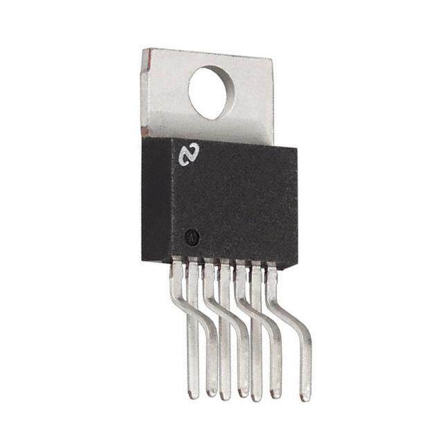
| 产品图片 |
|
| 产品型号 | LT1941EFE#PBF |
| PWM类型 | 电流模式 |
| rohs | 无铅 / 符合限制有害物质指令(RoHS)规范要求 |
| 产品系列 | - |
| 供应商器件封装 | 28-TSSOP-EP |
| 其它名称 | LT1941EFEPBF |
| 包装 | 管件 |
| 同步整流器 | 无 |
| 安装类型 | 表面贴装 |
| 封装/外壳 | 28-SOIC(0.173",4.40mm 宽)裸露焊盘 |
| 工作温度 | -40°C ~ 85°C |
| 标准包装 | 50 |
| 电压-输入 | 3.5 V ~ 25 V |
| 电压-输出 | 1.25 V ~ 40 V |
| 电流-输出 | 3A |
| 类型 | 降压(降压),升压(升压),反相,Sepic |
| 输出数 | 3 |
| 输出类型 | 可调式 |
| 频率-开关 | 1.1MHz |


PDF Datasheet 数据手册内容提取
LT1941 Triple Monolithic Switching Regulator FEATURES DESCRIPTION n Wide Input Range: 3.5V to 25V The LT®1941 is a triple current mode DC/DC converter n Three Switching Regulators with Internal Power with internal power switches. Two of the regulators are Switches: 3A Step-Down, 2A Step-Down, step-down converters with 3A and 2A power switches. 1.5A Inverting/Boost The third regulator can be confi gured as a boost, inverter n Antiphase Switching Reduces Ripple or SEPIC converter and has a 1.5A power switch. All n Independent Shutdown/Soft-Start Pins three converters are synchronized to a 1.1MHz oscillator. n Independent Power Good Indicators Ease Supply The two step-down converters run with opposite phase, Sequencing reducing input ripple current. The output voltages are n Input Voltage Power Good Indicators Monitor Input set with external resistor dividers and each regulator Supply has independent shutdown and soft-start circuits. Each n Uses Small Inductors and Ceramic Capacitors regulator generates a power good signal when its output n Constant 1.1MHz Switching Frequency is in regulation, easing power supply sequencing and n Thermally Enhanced 28-Lead TSSOP Package interfacing with microcontrollers and DSPs. The high switching frequency offers several advantages APPLICATIONS by permitting the use of small inductors and ceramic capacitors, leading to a very small triple output solution. n Cable Modems The constant switching frequency, combined with low n DSL Modems impedance ceramic capacitors, result in low, predictable n Distributed Power Regulation output ripple. With its wide input voltage range of 3.5V to n Wall Transformer Regulation 25V, the LT1941 regulates a broad array of power sources n Disk Drives from 4-cell batteries and 5V logic rails to unregulated wall n DSP Power transformers, lead acid batteries and distributed-power L, LT, LTC and LTM are registered trademarks of Linear Technology Corporation. All other supplies. trademarks are the property of their respective owners. TYPICAL APPLICATION VOUT1 VOUT2 VIN 4.7V TO 14V 130k 100k VIN 100k 100k 100k PGOOD1 PGOOD1 Start-Up Waveforms 5GOOD 5GOOD PGOOD2 PGOOD2 with Sequencing 12GOOD 12GOOD PGOOD3 PGOOD3 BOOST1 BOOST2 VOUT1 3μH 0.22μF LT1941 0.22μF 3.3μH RUN/SS 1.8V SW1 SW2 2V/DIV 2.4A 13.7k 10.7k VOUT2 FB1 FB2 3.3V VOUT1 3300pF 1000pF 1.4A 2V/DIV 33μF 7.32k 3.3k VC1 VC2 10k 2.49k 22μF 5VVO/DUTIV2 1.5nF 1.5nF RUNSS1 RUNSS2 SW3 BIAS1 VOUT3 10V/DIV 22μH 1μF NFB BIAS2 22nF VOUT3 IVIN(AVE) –12V 133k 13.7k VC3 1A/DIV 350mA* 22μH FB3 RUNSS3 PGOOD2 10μF 10μF GND 1.5nF 1.5k 5V/DIV 2ms/DIV 1941 F01b 1941 F01 *240mA AT VIN = 5V, 550mA AT VIN = 12V Figure 1. Triple Output Power Supply: 3.3V, 1.8V, –12V 1941fb 1
LT1941 ABSOLUTE MAXIMUM RATINGS PIN CONFIGURATION (Note 1) TOP VIEW V Pin ........................................................(–0.3V), 25V IN BOOST Pin Voltage ...................................................35V VIN 1 28 BIAS2 BOOST Above SW Pin ...............................................25V VIN 2 27 SW3 SW1 3 26 PGND BIAS1, BIAS2 Pins ....................................................25V PGOOD, 5GOOD, 12GOOD Pins .................................25V SW1 4 25 VIN BOOST1 5 24 BOOST2 RUN/SS, V , FB, NFB Pins ..........................................3V C PGOOD1 6 23 SW2 SW1, SW2 Voltage .....................................................V IN VC1 7 22 VIN SW3 Voltage .............................................................40V 29 FB1 8 21 PGOOD3 Maximum Junction Temperature (Note 6) ............125°C PGOOD2 9 20 FB3 Operating Ambient Temperature Range VC2 10 19 NFB (Note 2) ....................................................–40°C to 85°C FB2 11 18 VC3 Storage Temperature Range ..................–65°C to 150°C RUN/SS1 12 17 5GOOD Lead Temperature (Soldering, 10 sec)...................300°C RUN/SS2 13 16 12GOOD RUN/SS3 14 15 BIAS1 FE PACKAGE 28-LEAD PLASTIC TSSOP TJMAX = 125°C, θJA = 25°C/W EXPOSED PAD (PIN 29) IS GND, MUST BE SOLDERED TO PCB ORDER INFORMATION LEAD FREE FINISH TAPE AND REEL PART MARKING PACKAGE DESCRIPTION TEMPERATURE RANGE LT1941EFE#PBF LT1941EFE#TRPBF LT1941EFE 28-LEAD PLASTIC TSSOP –40°C to 85°C LEAD BASED FINISH TAPE AND REEL PART MARKING PACKAGE DESCRIPTION TEMPERATURE RANGE LT1941EFE LT1941EFE#TR LT1941EFE 28-LEAD PLASTIC TSSOP –40°C to 85°C Consult LTC Marketing for parts specifi ed with wider operating temperature ranges. For more information on lead free part marking, go to: http://www.linear.com/leadfree/ For more information on tape and reel specifi cations, go to: http://www.linear.com/tapeandreel/ ELECTRICAL CHARACTERISTICS The l denotes the specifi cations which apply over the full operating temperature range, otherwise specifi cations are at T = 25°C. V , V , V = 5V, V , V = 8V, unless otherwise noted. (Note 2) A IN BIAS1 BIAS2 BOOST1 BOOST2 PARAMETER CONDITIONS MIN TYP MAX UNITS Minimum Operating Voltage l 3.3 3.5 V V Quiescent Current Not Switching 2 3.5 mA IN BIAS1 Quiescent Current Not Switching 5 7.5 mA BIAS2 Quiescent Current Not Switching 1.6 2.2 mA Shutdown Current V = 0V 50 75 μA RUNSS1,2,3 Reference Voltage Line Regulation 5V < V < 25V 0.01 %/V IN V Source Current V = 0.6V 100 μA C C V Sink Current V = 0.6V 100 μA C C V Clamp Voltage 1.7 V C Switching Frequency l 0.9 1.1 1.35 MHz 1941fb 2
LT1941 ELECTRICAL CHARACTERISTICS The l denotes the specifi cations which apply over the full operating temperature range, otherwise specifi cations are at T = 25°C. V , V , V = 5V, V , V = 8V, unless otherwise noted. (Note 2) A IN BIAS1 BIAS2 BOOST1 BOOST2 PARAMETER CONDITIONS MIN TYP MAX UNITS Switching Phase SW1 to SW2 150 180 210 Deg SW1 to SW3 –30 0 30 Deg Foldback Frequency V = 0V 200 kHz FB RUN/SS Current 1 2 3 μA RUN/SS Threshold 0.4 0.6 V 5GOOD Threshold V Rising 4.5 V IN 5GOOD Voltage Output Low I = 125μA, V = 4V 0.2 0.4 V 5GOOD IN 5GOOD Leakage V = 2V 10 400 nA 5GOOD 12GOOD Threshold V Rising 10.8 V IN 12GOOD Voltage Output Low I = 125μA 0.2 0.4 V 12GOOD 12GOOD Leakage V = 2V, V = 12V 10 400 nA 12GOOD IN PGOOD Voltage Output Low I = 200μA 0.2 0.4 V PGOOD PGOOD Pin Leakage V = 2V 10 400 nA PGOOD 3A Step-Down FB1 Voltage 618 628 638 mV l 613 638 mV FB1 Pin Bias Current l 50 500 nA PGOOD1 Threshold Offset V Rising 54 mV FB Frequency Shift Threshold on FB1 0.35 V Error Amplifi er Transconductance 1700 μMhos Error Amplifi er Voltage Gain 500 V/V V Switching Threshold 0.9 V C V to Switch Current Gain 5 A/V C1 Switch 1 Current Limit (Note 3) V = 12V, V , V = 15V l 3 4.3 6 A IN BOOST1 BOOST2 Switch 1 V (Note 7) I = 2.5A 400 600 mV CESAT SW BOOST1 Pin Current I = 2.5A 40 60 mA SW Switch 1 Leakage Current 0.01 10 μA Minimum Boost Voltage Above Switch (Note 4) 1.8 2.5 V Maximum Duty Cycle l 78 88 % 2A Step-Down FB2 Voltage 618 628 638 mV l 613 638 mV FB2 Pin Bias Current l 50 500 nA PGOOD2 Threshold Offset V Rising 54 mV FB Frequency Shift Threshold on FB2 0.35 V Error Amplifi er Transconductance 1700 μMhos Error Amplifi er Voltage Gain 500 V/V V Switching Threshold 0.9 V C V to Switch Current Gain 3.6 A/V C2 Switch 2 Current Limit (Note 3) V = 12V, V , V = 15V l 2 2.9 4.1 A IN BOOST1 BOOST2 Switch 2 V (Note 7) I = 1.5A 450 600 mV CESAT SW BOOST2 Pin Current I = 1.5A 26 40 mA SW 1941fb 3
LT1941 ELECTRICAL CHARACTERISTICS The l denotes the specifi cations which apply over the full operating temperature range, otherwise specifi cations are at T = 25°C. V , V , V = 5V, V , V = 8V, unless otherwise noted. (Note 2) A IN BIAS1 BIAS2 BOOST1 BOOST2 PARAMETER CONDITIONS MIN TYP MAX UNITS Switch 2 Leakage Current 0.01 10 μA Minimum Boost Voltage Above Switch (Note 4) 1.8 2.5 V Maximum Duty Cycle l 78 88 % 1.5A Inverting/Boost FB3 Voltage 1.23 1.25 1.27 V l 1.22 1.27 V FB3 Pin Bias Current l 800 1400 nA NFB Voltage l –15 0 15 mV NFB Pin Bias Current l 60 500 nA NFB3 Voltage (V -V ) 1.212 1.24 1.258 V FB3 NFB l 1.205 1.260 V FB3 Pin Output Current V = 1.35V, V = –0.1V l 150 350 μA FB3 NFB PGOOD3 Threshold Offset V Rising 120 mV FB Error Amplifi er Transconductance 800 μMhos Error Amplifi er Voltage Gain 150 V/V V Switching Threshold 1.1 V C V to Switch Current Gain 5 A/V C3 Frequency Shift Threshold on FB3 0.65 V Switch 3 Current Limit (Note 5) l 1.5 2 2.9 A Switch 3 V I = 1A 240 320 mV CESAT SW BIAS2 Pin Current I = 1A 30 45 mA SW Switch 3 Leakage Current 0.01 10 μA Maximum Duty Cycle l 77 86 % Note 1: Stresses beyond those listed under Absolute Maximum Ratings Note 4: This is the minimum voltage across the boost capacitor needed to may cause permanent damage to the device. Exposure to any Absolute guarantee full saturation of the internal power switch. Maximum Rating condition for extended periods may affect device Note 5: Current limit is guaranteed by design and/or correlation to static reliability and lifetime. test. Note 2: The LT1941E is guaranteed to meet performance specifi cations Note 6: This IC includes overtemperature protection that is intended from 0°C to 70°C. Specifi cations over the –40°C to 85°C operating to protect the device during momentary overload conditions. Junction temperature range are assured by design, characterization and correlation temperature will exceed 125°C when overtemperature protection is active. with statistical process controls. Continuous operation above the specifi ed maximum operating junction Note 3: Current limit is guaranteed by design and/or correlation to static temperature may impair device reliability. test. Slope compensation reduces current limit at higher duty cycles. Note 7: Guaranteed by design, not 100% tested. 1941fb 4
LT1941 TYPICAL PERFORMANCE CHARACTERISTICS Effi ciency, V = 1.8V Effi ciency, V = 3.3V Effi ciency, V = –12V OUT1 OUT2 OUT3 90 90 90 VIN = 5V VIN = 5V VIN = 5V TA = 25°C TA = 25°C TA = 25°C 80 80 80 %) %) %) Y ( Y ( Y ( C C C N 70 N 70 N 70 CIE CIE CIE EFFI EFFI EFFI 60 60 60 50 50 50 0 0.5 1 1.5 2 2.5 0 0.25 0.5 0.75 1 1.25 1.5 0 50 100 150 200 250 300 LOAD CURRENT (A) LOAD CURRENT (A) LOAD CURRENT (mA) 1941 G01 1941 G07 1941 G08 SW1 V SW2 V SW3 V CESAT CESAT CESAT 500 600 500 TA = 25°C TA = 25°C TA = 25°C 500 400 400 V) V) V) E (m E (m400 E (m G300 G G300 A A A OLT OLT300 OLT V V V CH 200 CH CH 200 WIT WIT200 WIT S S S 100 100 100 0 0 0 0 0.5 1 1.5 2 2.5 3 0 0.5 1 1.5 2 0 0.25 0.5 0.75 1 1.25 1.5 SWITCH CURRENT (A) SWITCH CURRENT (A) SWITCH CURRENT (A) 1941 G02 1941 G09 1941 G10 SW1 Current Limit vs Duty Cycle SW2 Current Limit vs Duty Cycle BOOST2 Pin Current 5.0 3.0 40 TA = 25°C 4.5 TYPICAL 2.5 4.0 TYPICAL 30 MIT (A) 33..05 MINIMUM MIT (A) 2.0 MINIMUM NT (mA) NT LI 2.5 NT LI 1.5 URRE 20 RRE 2.0 RRE ST C U U 1.0 O C 1.5 C O B 10 1.0 0.5 0.5 0 0 0 0 20 40 60 80 100 0 20 40 60 80 100 0 0.5 1 1.5 2 DUTY CYCLE (%) DUTY CYCLE (%) SW2 PIN CURRENT (A) 1941 G03 1941 G06 1941 G11 1941fb 5
LT1941 TYPICAL PERFORMANCE CHARACTERISTICS BOOST1 Pin Current V vs Temperature V , V vs Temperature FB3 FB1 FB2 50 1.280 0.645 TA = 25°C 40 A) 1.265 0.635 m NT ( 30 CURRE V (V)FB1.250 V (V)FB0.625 T 20 S O O B 1.235 0.615 10 0 1.220 0.605 0 0.5 1 1.5 2 2.5 3 –50 –25 0 25 50 75 100 125 –50 –25 0 25 50 75 100 125 SW1 PIN CURRENT (A) TEMPERATURE (°C) TEMPERATURE (°C) 1941 G04 1941 G05 1941 G12 Switching Frequency Frequency vs Temperature vs % of Feedback Voltage I vs Temperature RUN/SS 1.3 1.2 3.0 TA = 25°C Hz) 1.0 2.5 FREQUENCY (MHz) 11..21 CHING FREQUENCY (M 000...468 UN/SS CURRENT (μA) 112...050 1.0 WIT R S 0.2 0.5 0.9 0 0 –50 –25 0 25 50 75 100 125 0 20 40 60 80 100 –50 –25 0 25 50 75 100 125 TEMPERATURE (°C) % OF FEEDBACK VOLTAGE TEMPERATURE (°C) 1941 G13 1941 G14 1941 G15 RUN/SS Thresholds Minimum Input Voltage Minimum Input Voltage vs Temperature V = 5V V = 3.3V OUT2 OUT2 1.4 8.0 6.0 DBOOST = CMDSH-3 DBOOST = CMDSH-3 1.2 TA = 25°C TA = 25°C RUN/SS THRESHOLDS (V) 10000.....08642 TO RUN TO SWITCH MINIMUM INPUT VOLTAGE (V) 77665.....05505 VVIINN TTOO SRTUANRT BTOBTINIIOOUEEPOOTDDUPSS TTTUTTOO TDDIIOODDEE MINIMUM INPUT VOLTAGE (V) 55443.....05505 VVIINN TTOO SRTUANRT BTOBTINIIOOUEEPOOTDDUPSS TTTUTTOO TDDIIOODDEE 0 5.0 3.0 –50 –25 0 25 50 75 100 125 1 10 100 1000 1 10 100 1000 TEMPERATURE (°C) LOAD CURRENT (mA) LOAD CURRENT (mA) 1941 G16 1941 G17 1941 G18 1941fb 6
LT1941 PIN FUNCTIONS V (Pins 1, 2, 22, 25): The V pins supply current to BIAS1 (Pin 15): The BIAS1 pin supplies the current to IN IN the LT1941’s internal circuitry and to the internal power the LT1941’s internal regulator. Tie this pin to the lowest switches. These pins must be tied to the same source and available voltage source above 2.35V (Either V , V or IN OUT locally bypassed. any other available supply). SW1, SW2, SW3 (Pins 3, 4, 23, 27): The SW pins are 12GOOD (Pin 16): The 12GOOD pin is the open-collector the outputs of the internal power switches. Connect these output of an internal comparator. 12GOOD remains low until pins to the inductors and switching diodes. V is within 10% of 12V. The pin pulls low when the part IN is in shutdown. Leave this pin unconnected if unused. BOOST1, BOOST2 (Pins 5, 24): The BOOST pins are used to provide drive voltages, higher than the input voltage, 5GOOD (Pin 17): The 5GOOD pin is the open-collector to the internal bipolar NPN power switches. Tie through output of an internal comparator. 5GOOD remains low until a diode from V or from V . V is within 10% of 5V. The pin pulls low when the part is OUT IN IN in shutdown. Leave this pin unconnected if unused. PGOOD1, PGOOD2, PGOOD3 (Pins 6, 9, 21): The PGOOD pins are the open-collector outputs of an internal compara- NFB (Pin 19): The LT1941 contains an op amp confi gured tor. PGOOD remains low until the FB pin is within 10% of with an output at FB3, noninverting terminal at GND and the fi nal regulation voltage. As well as indicating output an inverting terminal at NFB. Connect the feedback resistor regulation, the PGOOD pins can sequence the switching network virtual ground at this node if regulating negative regulators. Leave these pins unconnected if unused. The voltages. Otherwise, tie this node to FB3. PGOOD outputs are valid when V is greater than 3.5V IN PGND (Pin 26): Tie directly to local ground plane. and any of the RUN/SS pins are high. They are not valid when all RUN/SS pins are low. BIAS2 (Pin 28): The BIAS2 pin supplies the current to the driver of SW3. Tie this pin to the lowest available V , V , V (Pins 7, 10, 18): The V pins are the outputs C1 C2 C3 C voltage source above 2.5V (Either V , V or any other IN OUT of the internal error amps. The voltages on these pins available supply). control the peak switch currents. These pins are normally used to compensate the control loops. Each switching Exposed Pad (Pin 29): Ground. The underside Exposed regulator can be shut down by pulling its respective V Pad metal of the package provides both electrical contact C pin to ground with an NMOS or NPN transistor. to ground and good thermal contact to the printed circuit board. The Exposed Pad must be soldered to the circuit FB1, FB2, FB3 (Pins 8, 11, 20): The LT1941 regulates each board ground for proper operation. feedback pin to either 0.628V (FB1, FB2) or 1.25V (FB3). Connect the feedback resistor divider taps to these pins. RUN/SS1, RUN/SS2, RUN/SS3 (Pins 12, 13, 14): The RUN/SS pins are used to shut down the individual switching regulators and the internal bias circuits. They also provide a soft-start function. To shut down either regulator, pull the RUN/SS pin to ground with an open drain or collec- tor. Tie a capacitor from this pin to ground to limit switch current during start-up. If neither feature is used, leave these pins unconnected. 1941fb 7
LT1941 BLOCK DIAGRAM The LT1941 is a constant frequency, current mode, triple Each switcher contains an extra, independent oscillator to output regulator with internal power switches. The three perform frequency foldback during overload conditions. regulators share common circuitry including input source, This slave oscillator is normally synchronized to the master voltage reference and oscillator, but are otherwise inde- oscillator. A comparator senses when V is less than 50% FB pendent. Operation can be best understood by referring of its regulated value and switches the regulator from the to the Block Diagram. master oscillator to a slower slave oscillator. The V pin is FB less than 50% of its regulated value during start-up, short If the RUN/SS pins are tied to ground, the LT1941 is shut circuit and overload conditions. Frequency foldback helps down and draws 50μA from the input source tied to V . IN limit switch current under these conditions. Internal 2μA current sources charge external soft-start capacitors, generating voltage ramps at these pins. If any The switch drivers for SW1 and SW2 operate either of the RUN/SS pins exceed 0.6V, the internal bias circuits from V or from the BOOST pin. An external capacitor IN turn on, including the internal regulator, reference and and diode are used to generate a voltage at the BOOST 1.1MHz master oscillator. Each switching regulator will pin that is higher than the input supply. This allows the only begin to operate when its corresponding RUN/SS pin driver to saturate the internal bipolar NPN power switch reaches ≈1V. The master oscillator generates three clock for effi cient operation. signals, with the two signals for the step-down regulators The BIAS1 pin allows the internal circuitry to draw its out of phase by 180°. current from a lower voltage supply than the input, also The three switchers are current mode regulators. Instead reducing power dissipation and increasing effi ciency. If of directly modulating the duty cycle of the power switch, the voltage on the BIAS1 pin falls below 2.35V, then its the feedback loop controls the peak current in the switch quiescent current will fl ow from V . IN during each cycle. Compared to voltage mode control, cur- The BIAS2 pin allows the driver for SW3 to draw its rent mode control improves loop dynamics and provides current from a lower voltage supply than the input. This cycle-by-cycle current limit. reduces power dissipation within the part and increases The Block Diagram shows only one of the two step-down effi ciency. If the voltage on the BIAS2 pin falls below ≈2V, switching regulators. A pulse from the slave oscillator then SW3 will lock out and will not be able to turn on until sets the RS fl ip-fl op and turns on the internal NPN bipo- BIAS2 rises above ≈2.1V. lar power switch. Current in the switch and the external A power good comparator trips when the FB pin is at inductor begins to increase. When this current exceeds a 91% of its regulated value. The PGOOD output is an level determined by the voltage at V , current comparator C open-collector transistor that is off when the output is in C1 resets the fl ip-fl op, turning off the switch. The current regulation, allowing an external resistor to pull the PGOOD in the inductor fl ows through the external Schottky diode pin high. Power good is valid when the LT1941 is enabled and begins to decrease. The cycle begins again at the next and V > 3.5V. IN pulse from the oscillator. In this way, the voltage on the V pin controls the current through the inductor to the Input power good comparators monitor the input supply. C output. The internal error amplifi er regulates the output The 5GOOD and 12GOOD pins are open-collector outputs voltage by continually adjusting the V pin voltage. The of internal comparators. The 5GOOD pin remains low until C threshold for switching on the V pin is ≈1V and an active the input is within 10% of 5V. The 12GOOD pin remains C clamp of 1.7V limits the output current. The RUN/SS pin low until the input is within 10% of 12V. The 5GOOD and voltage also clamps the VC pin voltage. As the internal 12GOOD pins are valid as long as VIN is greater than current source charges the external soft-start capacitor, 1.1V. Both the 5GOOD and 12GOOD pins will sink current the current limit increases slowly. An internal op amp when the part is in shutdown, independent of the voltage allows the part to regulate negative voltages using only at VIN. two external resistors. 1941fb 8
LT1941 BLOCK DIAGRAM VIN 5GOOD BIAS1 + VIN 4.5V – 2μA RUN/SS1 CLK1 AINNTD R REEGF MAOSSTCER CCLLKK23 + 12GOOD 2μA RUN/SS2 s 10.8V – r o at Regul RUN/SS3 2μA VIN VIN g + CIN n hi witc (cid:164) 0.9V + – BOOST D2 n S SLOPE R w – Do SLAVE C1 S Q C3 p- CLK OSC e SW L1 St OUT Two + D1 C1 of One VC – 0.35V – FB R1 ERROR R2 AMP CF RC + 0.628V – CC RUN/SS ILIMIT CLAMP + 54mV PGOOD 1.7V + GND – VIN BIAS2 BOOST VC3 L3 SW3 D3 – C2 SW3 VOUT3 RUN/SS R S Q DRIVER Q1 C4 + or + at 1.25V + VIN Regul VOUT3 FB3 –ERAMROPR (cid:51) – 0.01Ω PGND L4A INVERLT4IBNG ching POSITFIOVRE R(E3XTERNAL)FB3 0.4V + GENREARMAPTOR SW3 C5 D4 C–6VOUT3 wit OUTPUTS R4 NFB OSCSILLALVAETOR S (EXTERNAL) – oost FB3 CLK3 B ng/ FOR R(E3XTERNAL) + erti NOEUGTAPTUIVTSE R4 NFB 0.6V – v (EXTERNAL) n NFB I –VOUT3 – PGOOD3 + + 1.12V – 1941 F02 Figure 2. Block Diagram of the LT1941 with Associated External Components 1941fb 9
LT1941 APPLICATIONS INFORMATION STEP-DOWN CONSIDERATIONS where V is the voltage drop of the catch diode (~0.4V) and F L is in μH. With this value the maximum load current will FB Resistor Network be 2.1A for SW1 and 1.4A for SW2, independent of input voltage. The inductor’s RMS current rating must be greater The output voltage is programmed with a resistor divider than the maximum load current and its saturation current (refer to the Block Diagram) between the output and the should be at least 30% higher. For highest effi ciency, the FB pin. Choose the resistors according to series resistance (DCR) should be less than 0.1Ω. Table 1 R1 = R2(V /628mV – 1) OUT lists several vendors and types that are suitable. R2 should be 10k or less to avoid bias current errors. Table 1. Inductors VALUE I DCR HEIGHT Input Voltage Range SAT PART NUMBER (μH) (A) (Ω) (mm) The minimum operating voltage is determined either by the Sumida LT1941’s undervoltage lockout of ~3.3V or by its maximum CR43-1R4 1.4 2.52 0.056 3.5 duty cycle. The duty cycle is the fraction of time that the CR43-2R2 2.2 1.75 0.071 3.5 internal switch is on and is determined by the input and CDRH3D16-1R5 1.5 1.55 0.040 1.8 output voltages: CDRH4D28-3R3 3.3 1.57 0.049 3.0 CDRH4D18-1R0 1.0 1.70 0.035 2.0 DC = (V + V )/(V – V + V ) OUT F IN SW F CDC5D23-2R2 2.2 2.50 0.03 2.5 where V is the forward voltage drop of the catch diode F CDRH5D28-2R6 2.6 2.60 0.013 3.0 (~0.4V) and V is the voltage drop of the internal switch SW Coilcraft (~0.3V at maximum load). This leads to a minimum input DO1606T-152 1.5 2.10 0.060 2.0 voltage of: DO1606T-222 2.2 1.70 0.070 2.0 VIN(MIN) = (VOUT + VF)/DCMAX – VF + VSW DO1608C-152 1.5 2.60 0.050 2.9 DO1608C-222 2.2 2.30 0.070 2.9 with DC = 0.78. MAX DO1608C-332 3.3 2.00 0.080 2.9 The maximum operating voltage is determined by the DO1608C-472 4.7 1.50 0.090 2.9 absolute maximum ratings of the V and BOOST pins IN MOS6020-222 2.2 2.15 0.035 2.0 and by the minimum duty cycle DC = 0.15: MIN MOS6020-332 3.3 1.8 0.046 2.0 V = (V + V )/DC – V + V MOS6020-472 4.7 1.5 0.050 2.0 IN(MAX) OUT F MIN F SW DO3314-222 2.2 1.6 0.200 1.4 This limits the maximum input voltage to ~14V with Toko V = 1.8V and ~19V with V = 2.5. Note that this is OUT OUT (D62F)847FY-2R4M 2.4 2.5 0.037 2.7 a restriction on the operating input voltage; the circuit (D73LF)817FY-2R2M 2.2 2.7 0.03 3.0 will tolerate input voltage transients up to the Absolute Maximum Rating. The optimum inductor for a given application may differ from the one indicated by this simple design guide. A Inductor Selection and Maximum Output Current larger value inductor provides a slightly higher maximum A good fi rst choice for the inductor value is load current and will reduce the output voltage ripple. If L = (V + V )/1.6 for SW1 OUT F L = (V + V )/1.1 for SW2 OUT F 1941fb 10
LT1941 APPLICATIONS INFORMATION your load is lower than the maximum load current, then duty cycles and decreases linearly to 1.6A at DC = 0.8. you can relax the value of the inductor and operate with The maximum output current is a function of the chosen higher ripple current. This allows you to use a physically inductor value: smaller inductor or one with a lower DCR resulting in I = I – ΔI /2 OUT(MAX) LIM L higher effi ciency. Be aware that if the inductance differs from the simple rule above, then the maximum load current = 3 • (1 – 0.25 • DC) – ΔIL/2 for SW1 will depend on input voltage. In addition, low inductance = 2 • (1 – 0.25 • DC) – ΔI /2 for SW2 L may result in discontinuous mode operation, which further Choosing an inductor value so that the ripple current is reduces maximum load current. For details of maximum small will allow a maximum output current near the switch output current and discontinuous mode operation, see current limit. Linear Technology’s Application Note AN44. Finally, for duty cycles greater than 50% (VOUT/VIN > 0.5), a minimum One approach to choosing the inductor is to start with the inductance is required to avoid subharmonic oscillations. simple rule given above, look at the available inductors See AN19. and choose one to meet cost or space goals. Then use these equations to check that the LT1941 will be able to The current in the inductor is a triangle wave with an average deliver the required output current. Note again that these value equal to the load current. The peak switch current equations assume that the inductor current is continu- is equal to the output current plus half the peak-to-peak ous. Discontinuous operation occurs when I is less inductor ripple current. The LT1941 limits its switch cur- OUT than ΔI /2. rent in order to protect itself and the system from overload L faults. Therefore, the maximum output current that the Output Capacitor Selection LT1941 will deliver depends on the switch current limit, the inductor value and the input and output voltages. For 5V and 3.3V outputs, a 10μF, 6.3V ceramic capacitor (X5R or X7R) at the output results in very low output volt- When the switch is off, the potential across the inductor age ripple and good transient response. For lower voltages, is the output voltage plus the catch diode drop. This gives 10μF is adequate for ripple requirements but increasing the peak-to-peak ripple current in the inductor: C will improve transient performance. Other types and OUT ΔIL = (1 – DC)(VOUT + VF)/(L • f) values will also work; the following discusses tradeoffs in output ripple and transient performance. where f is the switching frequency of the LT1941 and L is the value of the inductor. The peak inductor and switch The output capacitor fi lters the inductor current to generate current is: an output with low voltage ripple. It also stores energy in order to satisfy transient loads and stabilize the LT1941’s I = I = I + ΔI /2 SWPK LPK OUT L control loop. Because the LT1941 operates at a high To maintain output regulation, this peak current must be frequency, minimal output capacitance is necessary. In less than the LT1941’s switch current limit I . For SW1, LIM addition, the control loop operates well with or without I is at least 3A at low duty cycles and decreases linearly LIM the presence of output capacitor series resistance (ESR). to 2.4A at DC = 0.8. For SW2, I is at least 2A for at low LIM Ceramic capacitors, which achieve very low output ripple and small circuit size, are therefore an option. 1941fb 11
LT1941 APPLICATIONS INFORMATION You can estimate output ripple with the following Table 2. Low ESR Surface Mount Capacitors equations: VENDOR TYPE SERIES V = ΔI /(8 • f • C ) for ceramic capacitors Taiyo-Yuden Ceramic RIPPLE L OUT AVX Ceramic TPS and Tantalum V = ΔI • ESR for electrolytic capacitors (tantalum Kemet Tantalum T491,T494,T495 RIPPLE L Tantalum Organic T520 and aluminum) Aluminum Organic A700 where ΔI is the peak-to-peak ripple current in the inductor. Sanyo Tantalum or Aluminum Organic POSCAP L The RMS content of this ripple is very low so the RMS Panasonic Aluminum Organic SP CAP current rating of the output capacitor is usually not of TDK Ceramic concern. It can be estimated with the formula: Diode Selection I = ΔI /√12 C(RMS) L The catch diode (D1 from Figure 2) conducts current only Another constraint on the output capacitor is that it must during switch off time. Average forward current in normal have greater energy storage than the inductor; if the stored operation can be calculated from: energy in the inductor transfers to the output, the resulting voltage step should be small compared to the regulation I = I (V – V )/V D(AVG) OUT IN OUT IN voltage. For a 5% overshoot, this requirement indicates: The only reason to consider a diode with a larger current COUT > 10 • L • (ILIM/VOUT)2 rating than necessary for nominal operation is for the worst-case condition of shorted output. The diode current The low ESR and small size of ceramic capacitors make will then increase to the typical peak switch current. them the preferred type for LT1941 applications. Not all ceramic capacitors are the same, however. Many of the Peak reverse voltage is equal to the regulator input voltage. higher value capacitors use poor dielectrics with high Use a diode with a reverse voltage rating greater than the temperature and voltage coeffi cients. In particular, Y5V input voltage. Table 3 lists several Schottky diodes and and Z5U types lose a large fraction of their capacitance their manufacturers. with applied voltage and at temperature extremes. Table 3. Schottky Diodes Because loop stability and transient response depend on the value of C , this loss may be unacceptable. Use PART VR IAVE VF AT 1A VF AT 2A OUT NUMBER (V) (A) (mV) (mV) X7R and X5R types. On Semiconductor Electrolytic capacitors are also an option. The ESRs of MBRM120E 20 1 530 595 MBRM140 40 1 550 most aluminum electrolytic capacitors are too large to Diodes Inc. deliver low output ripple. Tantalum, as well as newer, B120 20 1 500 lower-ESR organic electrolytic capacitors intended for B130 30 1 500 B220 20 2 500 power supply use are suitable. Chose a capacitor with a B230 30 2 500 low enough ESR for the required output ripple. Because International Rectifi er the volume of the capacitor determines its ESR, both the 10BQ030 30 1 420 470 size and the value will be larger than a ceramic capacitor 20BQ030 30 2 470 that would give similar ripple performance. One benefi t is that the larger capacitance may give better transient response for large changes in load current. Table 2 lists several capacitor vendors. 1941fb 12
LT1941 APPLICATIONS INFORMATION Boost Pin Considerations in case V is held low while V is present. The circuit IN2 IN saves several components (both BOOST pins can be tied The capacitor and diode tied to the BOOST pin generate to D2). However, effi ciency may be lower and dissipation a voltage that is higher than the input voltage. In most in the LT1941 may be higher. Also, if V is absent the cases, a 0.18μF capacitor and fast switching diode (such IN2 LT1941 will still attempt to regulate the output, but will as the CMDSH-3 or MMSD914LT1) will work well. Figure 3 do so with low effi ciency and high dissipation because shows four ways to arrange the boost circuit. The BOOST the switch will not be able to saturate, dropping 1.5V to pin must be more than 2.5V above the SW pin for full 2V in conduction. effi ciency. For outputs of 3.3V and higher, the standard circuit (Figure 3a) is best. For outputs between 2.8V and The minimum operating voltage of an LT1941 application 3.3V, use a small Schottky diode (such as the BAT-54). is limited by the undervoltage lockout (3.5V) and by the For lower output voltages, the boost diode can be tied to maximum duty cycle. The boost circuit also limits the the input (Figure 3b). The circuit in Figure 3a is more ef minimum input voltage for proper start-up. If the input fi cient because the boost pin current comes from a lower voltage ramps slowly, or the LT1941 turns on when the voltage source. Finally, as shown in Figure 3c, the anode output is already in regulation, the boost capacitor may of the boost diode can be tied to another source that is not be fully charged. Because the boost capacitor charges at least 3V. For example, if you are generating 3.3V and with the energy stored in the inductor, the circuit will rely 1.8V and the 3.3V is on whenever the 1.8V is on, the 1.8V on some minimum load current to get the boost circuit boost diode can be connected to the 3.3V output. In any running properly. This minimum load will depend on input case, be sure that the maximum voltage at the BOOST pin and output voltages, and on the arrangement of the boost is less than 35V and the voltage difference between the circuit. The minimum load current generally goes to zero BOOST and SW pins is less than 25V. once the circuit has started. Even without an output load current, in many cases the discharged output capacitor will The boost circuit can also run directly from a DC voltage present a load to the switcher that will allow it to start. that is higher than the input voltage by more than 2.5V + V , F as in Figure 3d. The diode prevents damage to the LT1941 D2 D2 BOOST C3 BOOST C3 LT1941 LT1941 VIN VIN SW VOUT VIN VIN SW VOUT GND GND VBOOST – VSW(cid:32) VOUT VBOOST – VSW(cid:32) VIN MAX VBOOST(cid:32) VIN + VOUT MAX VBOOST(cid:32) 2VIN (3a) (3b) D2 D2 VIN2> 3V >VIN+V I3NV2 BOOST C3 BOOST LT1941 LT1941 VIN VIN SW VOUT VIN VIN SW VOUT GND GND VBOOST – VSW(cid:32) VIN2 MAX VBOOST – VSW(cid:32) VIN2 1941 F03 MAX VBOOST(cid:32) VIN2 + VIN MAX VBOOST(cid:32) VIN2 MINIMUM VALUE FOR VIN2 = 3V MINIMUM VALUE FOR VIN2 = VIN + 3V (3c) (3d) Figure 3. Generating the Boost Voltage 1941fb 13
LT1941 APPLICATIONS INFORMATION Converter with Backup Output Regulator Regulating Negative Output Voltages There is another situation to consider in systems where the The LT1941 contains an inverting op-amp with its nonin- output will be held high when the input to the LT1941 is verting terminal tied to ground and its output connected absent. If the V and one of the RUN/SS pins are allowed to the FB3 pin. Use this op-amp to generate a voltage at IN to fl oat, then the LT1941’s internal circuitry will pull its FB3 that is proportional to V . Choose the resistors OUT quiescent current through its SW pin. This is acceptable if according to: the system can tolerate a few mA of load in this state. With R3(cid:129) V both RUN/SS pins grounded, the LT1941 enters shutdown R4= OUT mode and the SW pin current drops to ~50mA. However, if 1.24V the V pin is grounded while the output is held high, then IN parasitic diodes inside the LT1941 can pull large currents –VOUT from the output through the SW pin and the VIN pin. A R4 NFB Schottky diode in series with the input to the LT1941, as shown in Figure 4, will protect the LT1941 and the system R3 from a shorted or reversed input. FB3 1941 AI02 PARASITIC DIODE Use 10k or larger, up to 20k for R3. D4 VIN VIN SW VOUT Duty Cycle Range The maximum duty cycle (DC) of the LT1941 inverter/boost LT1941 regulator is 77%. The duty cycle for a given application using the inverting topology is: 1941 F04 Figure 4. Diode D4 Prevents a Shorted Input from V Discharging a Backup Battery Tied to the Output DC= OUT V + V IN OUT INVERTER/BOOST CONSIDERATIONS The duty cycle for a given application using the boost topology is: Regulating Positive Output Voltages V –V The output voltage is programmed with a resistor divider DC= OUT IN V between the output and the FB pin. Choose the resistors OUT according to: The LT1941 can still be used in applications where the ⎛ V ⎞ DC, as calculated above, is above 77%; however, the part R3=R4⎜ OUT –1⎟ ⎝1.25V ⎠ must be operated in discontinuous mode so that the actual duty cycle is reduced. R4 should be 10k or less to avoid bias current errors. Inductor Selection NFB should be tied to FB3. Several inductors that work well with the LT1941 inverter/ VOUT boost regulator are listed in Table 4. Besides these, many other inductors will work. Consult each manufacturer R3 FB3 for detailed information and for their entire selection of related parts. Use ferrite core inductors to obtain the best R4 effi ciency. When using coupled inductors, choose one that 1941 AI01 1941fb 14
LT1941 APPLICATIONS INFORMATION can handle at least 1.5A of current without saturating and exceeds 20V, use the UPS140 (a 40V diode). These diodes ensure that the inductor has a low DCR (copper-wire resis- are rated to handle an average forward current of 1A. For tance) to minimize I2R power losses. If using uncoupled applications where the average forward current of the inductors, each inductor need only handle one-half of the diode is less than 0.5A, use an ON Semiconductor total switch current so that 0.75A per inductor is suffi cient. MBR0520L diode. The load current for boost, SEPIC and A 4.7μH to 15μH coupled inductor or two 15μH to 20μH inverting confi gurations is equal to the average diode uncoupled inductors will usually be the best choice for current. most LT1941 inverter designs. A 4.7μH to 15μH inductor will be the best choice for most LT1941 boost designs. In BIAS2 Pin Considerations this case, the single inductor must carry the entire 1.5A The BIAS2 pin provides the drive current for the inverter/ peak switch current. boost switch. The voltage source on the BIAS2 line should be able to supply the rated current and be at a minimum Table 4. Inductors of 2.5V. For highest effi ciency, use the lowest voltage VALUE I DCR HEIGHT SAT(DC) PART NUMBER (μH) (A) (Ω) (mm) source possible (VOUT = 3.3V, for example) to minimize Coiltronics the VBIAS2 • IBIAS2 power loss inside the part. TP3-4R7 4.7 1.5 0.181 2.2 TP4-100 10 1.5 0.146 3.0 INPUT CAPACITOR SELECTION Sumida Bypass the input of the LT1941 circuit with a 10μF or CDRH6D38NP-6R2 6.2 2.5 20m 3.8 higher ceramic capacitor of X7R or X5R type. A lower CDRH6D38NP-7R4 7.4 2.3 23m 3.8 value or a less expensive Y5V type will work if there is CDRH6D38NP-100 10 2.0 28m 3.8 additional bypassing provided by bulk electrolytic capaci- tors, or if the input source impedance is low. The following Output Capacitor Selection paragraphs describe the input capacitor considerations in more detail. Use low ESR (equivalent series resistance) capacitors at the output to minimize the output ripple voltage. Multilayer Step-down regulators draw current from the input sup- ceramic capacitors are an excellent choice; they have an ply in pulses with very fast rise and fall times. The input extremely low ESR and are available in very small pack- capacitor is required to reduce the resulting voltage ripple ages. X7R dielectrics are preferred, followed by X5R, as at the LT1941 input and to force this switching current these materials retain their capacitance over wide voltage into a tight local loop, minimizing EMI. The input capaci- and temperature ranges. A 4.7μF to 20μF output capacitor tor must have low impedance at the switching frequency is suffi cient for most LT1941 applications. Solid tantalum to do this effectively and it must have an adequate ripple or OS-CON capacitors will work but they will occupy more current rating. With two switchers operating at the same board area and will have a higher ESR than a ceramic frequency but with different phases and duty cycles, cal- capacitor. Always use a capacitor with a suffi cient volt- culating the input capacitor RMS current is not simple; age rating. however, a conservative value is the RMS input current for the channel that is delivering the most power (V OUT Diode Selection times I ): OUT A Schottky diode is recommended for use with the LT1941 ( ) V V –V I inverter/boost regulator. The Microsemi UPS120 is a very C =I (cid:129) OUT IN OUT < OUT IN(RMS) OUT good choice. Where the input to output voltage differential V 2 IN 1941fb 15
LT1941 APPLICATIONS INFORMATION and is largest when V = 2 V (50% duty cycle). As LT1941 does not depend on the ESR of the output capacitor IN OUT the second, lower power channel draws input current, the for stability so you are free to use ceramic capacitors to input capacitor’s RMS current actually decreases as the achieve low output ripple and small circuit size. out-of-phase current cancels the current drawn by the The components tied to the V pin provide frequency C higher power channel. The ripple current contribution compensation. Generally, a capacitor and a resistor in from the third channel will be minimal. Considering that series to ground determine loop gain. In addition, there the maximum load current from a single channel is ~2.8A, is a lower value capacitor in parallel. This capacitor fi lters RMS ripple current will always be less than 1.4A. noise at the switching frequency and is not part of the The high frequency of the LT1941 reduces the energy loop compensation. storage requirements of the input capacitor, so that the Loop compensation determines the stability and transient capacitance required is often less than 10μF. The combi- performance. Designing the compensation network is a bit nation of small size and low impedance (low equivalent complicated and the best values depend on the application series resistance or ESR) of ceramic capacitors makes and the type of output capacitor. A practical approach is to them the preferred choice. The low ESR results in very start with one of the circuits in this data sheet that is similar low voltage ripple. Ceramic capacitors can handle larger to your application and tune the compensation network magnitudes of ripple current than other capacitor types to optimize the performance. Check stability across all of the same value. Use X5R and X7R types. operating conditions, including load current, input voltage An alternative to a high value ceramic capacitor is a lower and temperature. The LT1375 data sheet contains a more value along with a larger electrolytic capacitor, for example thorough discussion of loop compensation and describes a 1μF ceramic capacitor in parallel with a low ESR tantalum how to test the stability using a transient load. Application capacitor. For the electrolytic capacitor, a value larger than Note 76 is an excellent source as well. 10μF will be required to meet the ESR and ripple current Figure 5 shows an equivalent circuit for the LT1941 control requirements. Because the input capacitor is likely to see loop. The error amp is a transconductance amplifi er with high surge currents when the input source is applied, tan- fi nite output impedance. The power section, consisting of talum capacitors should be surge rated. The manufacturer the modulator, power switch and inductor is modeled as may also recommend operation below the rated voltage a transconductance amplifi er generating an output cur- of the capacitor. Be sure to place the 1μF ceramic as close rent proportional to the voltage at the V pin. Note that C as possible to the V and GND pins on the IC for optimal IN the output capacitor integrates this current and that the noise immunity. capacitor on the V pin (C ) integrates the error ampli- C C A fi nal caution is in order regarding the use of ceramic fi er output current, resulting in two poles in the loop. In capacitors at the input. A ceramic input capacitor can most cases, a zero is required and comes either from the combine with stray inductance to form a resonant tank output capacitor ESR or from a resistor in series with C . C circuit. If power is applied quickly (for example by plugging This model works well as long as the inductor current the circuit into a live power source), this tank can ring, ripple is not too low (ΔI > 5% I ) and the loop RIPPLE OUT doubling the input voltage and damaging the LT1941. The crossover frequency is less than ƒ /5. A phase lead SW solution is to either clamp the input voltage or dampen the capacitor (C ) across the feedback divider may improve PL tank circuit by adding a lossy capacitor in parallel with the the transient response. ceramic capacitor. For details, see Application Note 88. The equivalent circuit for the LT1941 inverter control loop is slightly different than is shown in Figure 5. The feedback Frequency Compensation resistors are connected as shown for negative outputs in The LT1941 uses current mode control to regulate the Figure 2. The operational amplifi er is fast enough to have output. This simplifi es loop compensation. In particular, the minimal effect on the loop dynamics. 1941fb 16
LT1941 APPLICATIONS INFORMATION single capacitor providing soft-start. The internal current Table 5. Converter Equivalent Model Parameters sources will charge these pins to ~2V. STEP-DOWN1 STEP-DOWN2 BOOST INVERTER VFB 0.628V 0.628V 1.25 1.24 The RUN/SS pins provide a soft-start function that limits R 500kΩ 500kΩ 500kΩ 500kΩ peak input current to the circuit during start-up. This helps O g 1700μmho 1700μmho 800μmho 800μmho to avoid drawing more current than the input source can ma g 5mho 3.6mho V • 5mho V • 5mho supply or glitching the input supply when the LT1941 is mp IN IN VOUT –|VOUT| enabled. The RUN/SS pins do not provide an accurate delay to start or an accurately controlled ramp at the LT1941 output voltage, both of which depend on the output ca- CURRENT MODE VSW pacitance and the load current. However, the power good POWER STAGE OUTPUT gmp ERROR indicators can be used to sequence the three outputs, as AMPLIFIER R1 CPL described below. FB – gma 500k + VFB ESR+ C1 POWER GOOD INDICATORS GND VC C1 The PGOOD pin is the open-collector output of an internal POLYMER CERAMIC comparator. PGOOD remains low until the FB pin is within R2 OR RC CF TANTALUM 10% of the fi nal regulation voltage. Tie the PGOOD to any supply with a pull-up resistor that will supply less than CC 200μA. Note that this pin will be open when the LT1941 is in shutdown mode (all three RUN/SS pins at ground) 1941 F05 regardless of the voltage at the FB pin. PGOOD is valid Figure 5. Model for Loop Response when the LT1941 is enabled (any RUN/SS pin is high) and SOFT-START AND SHUTDOWN VIN is greater than ~3.5V. The RUN/SS (Run/Soft-Start) pins are used to place the The 5GOOD and 12GOOD pins are also open-collector individual switching regulators and the internal bias cir- outputs of internal comparators. The 5GOOD pin remains cuits in shutdown mode. They also provide a soft-start low until the input is within 10% of 5V. Tie the 5GOOD and function. To shut down a regulator, pull its RUN/SS pin to 12GOOD pins to any supply with a pull-up resistor that will ground with an open drain or collector. If all three RUN/SS supply less than 100μA. The 12GOOD pin remains low until pins are pulled to ground, the LT1941 enters its shutdown the input is within 10% of 12V. The 5GOOD and 12GOOD mode with all regulators off and quiescent current reduced pins are valid as long as VIN is greater than 1.1V. Both the to ~50mA. Internal 2μA current sources pull up on each 5GOOD and 12GOOD pins will sink current when the part pin. If any RUN/SS pin reaches ~0.6V, the internal bias is in shutdown, independent of the voltage at VIN. circuits start and the quiescent currents increase to their Output Sequencing nominal levels. The PG and RUN/SS pins can be used to sequence the If a capacitor is tied from the RUN/SS pin to ground, then three outputs. Figure 6 shows several circuits to do this. the internal pull-up current will generate a voltage ramp on The techniques shown to sequence two channels can be this pin. This voltage clamps the V pin, limiting the peak C extended to sequence the third. In each case channel 1 switch current and therefore input current during start-up. starts fi rst. Note that these circuits sequence the outputs A good value for the soft-start capacitor is C /10,000, OUT during start-up. When shut down the three channels turn where C is the value of the output capacitor. OUT off simultaneously. The RUN/SS pins can be left fl oating if the shutdown feature is not used. They can also be tied together with a 1941fb 17
LT1941 APPLICATIONS INFORMATION In Figure 6a, a larger capacitor on RUN/SS2 delays channel Finally, be aware that the circuit in Figure 6d does not 2 with respect to channel 1. The soft-start capacitor on work, because the power good comparators are disabled RUN/SS2 should be at least twice the value of the capacitor in shutdown. on RUN/SS1. A larger ratio may be required, depending on the output capacitance and load on each channel. Make PCB LAYOUT sure to test the circuit in the system before deciding on For proper operation and minimum EMI, care must be taken fi nal values for these capacitors. during printed circuit board (PCB) layout. Figure 7 shows The circuit in Figure 6b requires the fewest components, the high current paths in the step-down regulator circuit. with both channels sharing a single soft-start capacitor. Note that in the step-down regulators large, switched The power good comparator of channel 1 disables chan- currents fl ow in the power switch, the catch diode and nel 2 until output 1 is in regulation. the input capacitor. In the inverter/boost regulator large, For independent control of channel 2, use the circuit in switched currents fl ow through the power switch, the Figure 6c. The capacitor on RUN/SS1 is smaller than the switching diode, and either the output capacitor in boost capacitor on RUN/SS2. This allows the LT1941 to start up confi guration, or the tank capacitor in the inverter con- and enable its power good comparator before RUN/SS2 fi guration. The loop formed by these components should gets high enough to allow channel 2 to start switching. be as small as possible. Place these components, along Channel 2 only operates when it is enabled with the external with the inductor and output capacitor, on the same side control signals and output 1 is in regulation. of the circuit board and connect them on that layer. Place a local, unbroken ground plane below these components The circuit in Figure 6a leaves both power good indica- and tie this ground plane to system ground at one loca- tors free. However, the circuits in Figures 6b and 6c have tion, ideally at the ground terminal of the output capacitor another advantage. As well as sequencing the two outputs C2. Additionally, keep the SW and BOOST nodes as small at start-up, they also disable channel 2 if output 1 falls as possible. out of regulation (due to a short circuit or a collapsing input voltage). RUN/SS1 RUN/SS1 VC2 OFF ON 1nF OFF ON 1nF LT1941 LT1941 RUN/SS2 RUN/SS2 PG1 GND GND 2.2nF (6a) Channel 2 is Delayed (6b) Fewest Components RUN/SS1 RUN/SS1 OFF ON 1nF LT1941 OFF ON 1nF LT1941 PG1 PG1 RUN/SS2 RUN/SS2 GND GND OFF2 ON2 1.5nF 1.5nF 1941 F06 (6c) Independent Control of Channel 2 (6d) Doesn't Work ! Figure 6. Several Methods of Sequencing Two Ouputs. Channel 1 Starts First 1941fb 18
LT1941 APPLICATIONS INFORMATION VIN SW VIN SW GND GND (a) (b) VSW VIN SW L1 IC1 C1 D1 C2 GND 1941 F07 (c) Figure 7. Subtracting the Current when the Switch is ON (a) From the Current when the Switch is OFF (b) Reveals the Path of the High Frequency Switching Current (c) Keep This Loop Small. The Voltage on the SW and BOOST Nodes will also be Switched; Keep these Nodes as Small as Possible. Finally, Make Sure the Circuit is Shielded with a Local Ground Plane C9 GND VIN L3 L4 C12 VOUT3 CIN1 D3 VOUT1 C10 GND D2 C11 D5 D1C8 U1 C7 VOUT2 L1 CIN2 D4 GND GND 1941 F08 PLACE VIAS UNDER GROUND PAD TO GROUND PLANE FOR GOOD THERMAL CONDUCTIVITY Figure 8. Power Path Components and Topside Layout THERMAL CONSIDERATIONS (or junction) to ambient can be reduced to θ = 25°C/W JA or less. With 100 LFPM airfl ow, this resistance can fall The PCB must provide heat sinking to keep the LT1941 by another 25%. Further increases in airfl ow will lead to cool. The Exposed Pad on the bottom of the package must lower thermal resistance. be soldered to a ground plane. This ground should be tied to other copper layers below with thermal vias; these lay- Because of the large output current capability of the LT1941, ers will spread the heat dissipated by the LT1941. Place it is possible to dissipate enough heat to raise the junction additional vias near the catch diodes. Adding more copper temperature beyond the absolute maximum of 125°C. If to the top and bottom layers and tying this copper to the two of the channels are running at full output current, the internal planes with vias can reduce thermal resistance third channel may have reduced output current capability, further. With these steps, the thermal resistance from die limited by the maximum junction temperature. The output 1941fb 19
LT1941 APPLICATIONS INFORMATION current capability of the third channel can be calculated Note that decreasing θ increases the power output JA from the output currents and voltages of the other chan- capability. The power output capability of the individual nels, the switching regulator effi ciency (η), the ambient channels can be calculated from the following: temperature (T ), the maximum junction temperature A Channel 1 Output Power (P1) = V1 • I (T ) and the thermal resistance from junction to ambi- 1 JMAX Channel 2 Output Power (P2) = V2 • I ent (θ ) as follows: 2 JA Channel 3 Output Power (P3) = V3 • I 3 T –T Total Output Power (P123) = P /η = P1 + P2 + P3 P = JMAX A DISS DISS θ JA Figure 9 shows power output capability if overall system P effi ciency (η) is 75% and maximum allowable power P3= DISS –V1(cid:129)I –V2(cid:129)I 1–η 1 2 dissipation (PDISS) is either 1W or 2W. For example, if al- lowable power dissipation is 2W, Channel 3 output power PP3 I = is 2W and Channel 2 output power is 1W, then Channel 1 3 V3 output power can be up to 5W. Example: LT1941 at V1 = 2.5V, I = 2A, V2 = 3.3V, I = 1 2 1A, V3 = 12V, η = 80%, TA = 75°C, TJMAX = 125°C, θJA = RELATED LINEAR TECHNOLOGY PUBLICATIONS 25°C/W: Application notes 19, 35, 44, 76 and 88 contain more 125°C–75°C P = =2W detailed descriptions and design information for buck DISS 25°C/W regulators and other switching regulators. The LT1375 2W data sheet has a more extensive discussion of output P3= –2.5V(cid:129)2A––3.3V(cid:129)1A=1.7W 1–0.8 ripple, loop compensation, and stability testing. Design 1.7W Notes 100 and 318 show how to generate a dual polarity I = =0.141A 3 output supply using a buck regulator. 12V Power Output Capability for P = 2W, η = 0.75 Power Output Capability for P = 1W, η = 0.75 DISS DISS 6 3.0 S) S) TT 5 CHANNEL 3 TT 2.5 CHANNEL 3 WA OUTPUT POWER (P3) WA OUTPUT POWER (P3) R ( P3 = 2W R ( P3 = 1W E 4 E 2.0 W W O O P P UT 3 UT 1.5 P P T P3 = 4W T P3 = 2W U U O O 2 2 2 1.0 EL P3 = 6W EL P3 = 3W N N N N A 1 A 0.5 H H C C 0 0 0 1 2 3 4 5 6 0 1 2 3 CHANNEL 1 OUTPUT POWER (WATTS) CHANNEL 1 OUTPUT POWER (WATTS) 1941 F09a 1941 F09b Figure 9. Power Output Capability of an Individual Channel Depends on the Output Power of the Other Channels 1941fb 20
LT1941 APPLICATIONS INFORMATION SLIC Power Supply –21.6V, –65V, 3.3V and 1.8V with Soft-Start VOUT1 VOUT2 VIN 5V R2 R1 R3 R8 R9 130k 100k VIN 100k 100k 100k PGOOD1 PGOOD1 5GOOD 5GOOD PGOOD2 PGOOD2 12GOOD 12GOOD PGOOD3 PGOOD3 D1 D2 BOOST1 BOOST2 C1 C2 VOUT1 L1 3μH 0.22μF LT1941 0.22μF L2 3.3μH 1.8V SW1 SW2 2.4A R7 R12 13.7k 10.7k VOUT2 FB1 FB2 3.3V C12 3300pF C13 1000pF 1.4A C3 D3 VC1 VC2 D4 C4 33μF R6 R4 C14 C15 R10 R11 22μF 7.32k 3.3k 1.5nF 1.5nF 10k 2.49k RUNSS1 RUNSS2 SW3 BIAS1 L3 NFB BIAS2 C16 4700pF 2.7μH R15 R13 R5 1Ω 178k 10.2k VC3 C5 FB3 RUNSS3 R14 C6 315μVF PGND GND C1.157nF 15k 10μF 1941 TA01 D5 C7 NOTE: TOTAL OUTPUT POWER OF VOUT3 AND VOUT4 NOT TO EXCEED 1.9W C1 TO C11: X5R OR X7R 4.7μF D1, D2: CMDSH-3 VOUT3 25V D3: B220A –21.6V D4: MBRM120L 72mA D5 TO D7: BAV99 OR EQUIVALENT C8 D6 1μF 35V C9 4.7μF 25V C10 D7 1μF 35V C11 4.7μF 25V VOUT4 –65V 30mA 1941fb 21
LT1941 TYPICAL APPLICATIONS Quadruple Output Power Supply: ±12V, 3.3V and 2.5V with Soft-Start VIN VOUT1 VOUT2 VOUT3 5V R2 R1 R3 R8 R9 130k 100k VIN 100k 100k 100k PGOOD1 PGOOD1 5GOOD 5GOOD PGOOD2 PGOOD2 12GOOD 12GOOD PGOOD3 PGOOD3 D1 D2 BOOST1 BOOST2 C1 C2 VOUT1 L1 3μH 0.22μF LT1941 0.22μF L2 3.3μH 2.5V SW1 SW2 2.3A R7 R12 10.2k 10.7k VOUT2 FB1 FB2 3.3V C10 1000pF C12 1000pF 1.4A C3 D3 VC1 VC2 D4 C4 33μF R6 R4 C11 C13 R10 R11 22μF 3.4k 10k 1.5nF 1.5nF 10k 2.49k RUNSS1 RUNSS2 L3 10μH SW3 BIAS1 C9 1Ω VOUT3 D5 4.7μF C5 R13 NFB BIAS2 C14 6800pF 12V 4.7μF 118k VC3 100mA FB3 RUNSS3 R14 C6 C7 D8 D7 R135.7k PGND GND C1.155nF 2.2k 10μF 10μF 1941 TA02 C8 D6 C1 TO C9: X5R OR X7R VOUT4 10μF D1, D2: CMDSH-3 –12V D3: B220A 100mA D4: MBRM120L D5 TO D8: MBR0540 Triple Output Power Supply: 3.3V, 1.8V and –12V VOUT1 VOUT2 VIN 4.7V TO 14V 130k 100k 100k 100k 100k VIN PGOOD1 PGOOD1 5GOOD 5GOOD PGOOD2 PGOOD2 12GOOD 12GOOD PGOOD3 PGOOD3 BOOST1 BOOST2 C1 C2 VOUT1 3μH 0.22μF LT1941 0.22μF 3.3μH 1.8V SW1 SW2 2.4A 13.7k 10.7k VOUT2 FB1 FB2 3.3V C8 3300pF C10 1000pF 1.4A C3 VC1 VC2 C4 33μF 7.32k 3.3k C9 C11 10k 2.49k 22μF 1.5nF 1.5nF RUNSS1 RUNSS2 SW3 BIAS1 22μH C5 NFB BIAS2 C12 22nF VOUT3 1μF –12V 133k 13.7k VC3 350mA* 22μH FB3 RUNSS3 C6 C7 GND C13 1.5k 1.5nF 10μF 10μF 1941 F01 *240mA AT VIN = 5V, 550mA AT VIN = 12V C1-C7: X5R OR X7R D1, D2: CMDSH-3 D3: B220A D4: UPS120 D5: B130 1941fb 22
LT1941 PACKAGE DESCRIPTION FE Package 28-Lead Plastic TSSOP (4.4mm) (Reference LTC DWG # 05-08-1663) Exposed Pad Variation EB 4.75 9.60 – 9.80* (.187) (.378 – .386) 4.75 (.187) 28 2726252423222120 19181716 15 6.60 ±0.10 2.74 EXPOSED 4.50 ±0.10 (.108) PAD HEAT SINK SEE NOTE 4 ON BOTTOM OF 6.40 0.45 ±0.05 PACKAGE 2.74 (.252) (.108) BSC 1.05 ±0.10 0.65 BSC RECOMMENDED SOLDER PAD LAYOUT 1 2 3 4 5 6 7 8 9 10 1112 1314 1.20 4.30 – 4.50* (.047) (.169 – .177) 0.25 MAX REF 0° – 8° 0.65 0.09 – 0.20 0.50 – 0.75 (.0256) 0.05 – 0.15 (.0035 – .0079) (.020 – .030) BSC (.002 – .006) 0.195 – 0.30 (.0077 – .0118) FE28 (EB) TSSOP 0204 TYP NOTE: 1. CONTROLLING DIMENSION: MILLIMETERS 4. RECOMMENDED MINIMUM PCB METAL SIZE 2. DIMENSIONS ARE INMILLIMETERS FOR EXPOSED PAD ATTACHMENT (INCHES) *DIMENSIONS DO NOT INCLUDE MOLD FLASH. MOLD FLASH 3. DRAWING NOT TO SCALE SHALL NOT EXCEED 0.150mm (.006") PER SIDE 1941fb Information furnished by Linear Technology Corporation is believed to be accurate and reliable. 23 However, no responsibility is assumed for its use. Linear Technology Corporation makes no representa- tion that the interconnection of its circuits as described herein will not infringe on existing patent rights.
LT1941 RELATED PARTS PART NUMBER DESCRIPTION COMMENTS LT1613 550mA (I ), 1.4MHz, High Effi ciency Step-Up DC/DC Converter V : 0.9V to 10V, V = 34V, I = 3mA, I < 1μA, SW IN OUT(MAX) Q SD ThinSOT™ Package LT1615/LT1615-1 300mA/80mA (I ), High Effi ciency Step-Up DC/DC Converter V : 1V to 15V, V = 34V, I = 20μA, I < 1μA, SW IN OUT(MAX) Q SD ThinSOT Package LT1617/LT1617-1 300mA/100mA (I ), 1.2MHz/2.2MHz, High Effi ciency Inverting V : 1.2V to 15V, V = –34V, I = 20μA, I < 1μA, SW IN OUT(MAX) Q SD DC/DC Converter ThinSOT Package LT1618 1.5A (I ), 1.25MHz, High Effi ciency Step-Up DC/DC Converter V : 1.6V to 18V, V = 35V, I = 1.8mA, I < 1μA, SW IN OUT(MAX) Q SD MS10 Package LT1930/LT1930A 1A (I ), 1.2MHz/2.2MHz, High Effi ciency Step-Up V : 2.6V to 16V, V = 34V, I = 4.2mA/5.5mA, I < 1μA, SW IN OUT(MAX) Q SD DC/DC Converter ThinSOT Package LT1931/LT1931A 1A (I ), 1.2MHz/2.2MHz, High Effi ciency Inverting V : 2.6V to 16V, V = –34V, I = 5.8mA, I < 1μA, SW IN OUT(MAX) Q SD DC/DC Converter ThinSOT Package LT1943 Quad Output, 2.6A Buck, 2.6A Boost, 0.3A Boost, 0.4A Inverter V : 4.5V to 22V, V = 40V, I = 10mA, I < 35μA, IN OUT(MAX) Q SD 1.2MHz TFT DC/DC Converter TSSOP28E Package LT1944-1 Dual Output 150mA (I ), Constant Off-Time, High Effi ciency V : 1.2V to 15V, V = 34V, I = 20μA, I < 1μA, SW IN OUT(MAX) Q SD Step-Up DC/DC Converter MS10 Package LT1944 Dual Output 350mA (I ), Constant Off-Time, High Effi ciency V : 1.2V to 15V, V = 34V, I = 20μA, I < 1μA, SW IN OUT(MAX) Q SD Step-Up DC/DC Converter MS10 Package LT1945 Dual Output Pos/Neg 350mA (I ), Constant Off-Time, High V : 1.2V to 15V, V = ±34V, I = 20μA, I < 1μA, SW IN OUT(MAX) Q SD Effi ciency Step-Up DC/DC Converter MS10 Package LT1946/LT1946A 1.5A (I ), 1.2MHz/2.7MHz, High Effi ciency Step-Up V : 2.45V to 16V, V = 34V, I = 3.2mA, I < 1μA, SW IN OUT(MAX) Q SD DC/DC Converter MS8 Package LT1961 1.5A (I ), 1.25MHz, High Effi ciency Step-Up DC/DC Converter V : 3V to 25V, V = 35V, I = 0.9mA, I < 6μA, SW IN OUT(MAX) Q SD MS8E Package LT3436 3A (I ), 1MHz, 34V Step-Up DC/DC Converter V : 3V to 25V, V = 34V, I = 0.9mA, I < 6μA, SW IN OUT(MAX) Q SD TSSOP16E Package LT3461/LT3461A 300mA (I ), High Effi ciency Step-Up DC/DC Converter with V : 2.5V to 16V, V = 38V, I = 2.8mA, I < 1μA, SW IN OUT(MAX) Q SD Integrated Schottky and Soft-Start ThinSOT Package LT3463 Dual Output Pos/Neg 250mA (I ), Constant Off-Time, High V : 2.4V to 15V, V = ±40V, I = 40μA, I < 1μA, SW IN OUT(MAX) Q SD Effi ciency Step-Up DC/DC Converter with Integrated Schottkys 3mm × 3mm DFN10 Package LT3464 85mA (I ), High Effi ciency Step-Up DC/DC Converter with V : 2.3V to 10V, V = 34V, I = 25μA, I < 1μA, SW IN OUT(MAX) Q SD Integrated Schottky and PNP Disconnect ThinSOT Package ThinSOT is a trademark of Linear Technology Corporation. 1941fb 24 Linear Technology Corporation LT 0409 REV B • PRINTED IN USA 1630 McCarthy Blvd., Milpitas, CA 95035-7417 (408) 432-1900 ● FAX: (408) 434-0507 ● www.linear.com © LINEAR TECHNOLOGY CORPORATION 2004