ICGOO在线商城 > 集成电路(IC) > PMIC - 稳压器 - DC DC 开关稳压器 > LT1935ES5#TRMPBF

 Datasheet下载
- 型号: LT1935ES5#TRMPBF
- 制造商: LINEAR TECHNOLOGY
- 库位|库存: xxxx|xxxx
- 要求:
| 数量阶梯 | 香港交货 | 国内含税 |
| +xxxx | $xxxx | ¥xxxx |
查看当月历史价格
查看今年历史价格
LT1935ES5#TRMPBF产品简介:
ICGOO电子元器件商城为您提供LT1935ES5#TRMPBF由LINEAR TECHNOLOGY设计生产,在icgoo商城现货销售,并且可以通过原厂、代理商等渠道进行代购。 LT1935ES5#TRMPBF价格参考。LINEAR TECHNOLOGYLT1935ES5#TRMPBF封装/规格:PMIC - 稳压器 - DC DC 开关稳压器, Boost, Flyback, SEPIC Switching Regulator IC Positive Adjustable 1.265V 1 Output 2A (Switch) SOT-23-5 Thin, TSOT-23-5。您可以下载LT1935ES5#TRMPBF参考资料、Datasheet数据手册功能说明书,资料中有LT1935ES5#TRMPBF 详细功能的应用电路图电压和使用方法及教程。
| 参数 | 数值 |
| 产品目录 | 集成电路 (IC) |
| 描述 | IC REG BST FLYBK SEPIC TSOT23-5 |
| 产品分类 | |
| 品牌 | Linear Technology |
| 数据手册 | http://www.linear.com/docs/2339 |
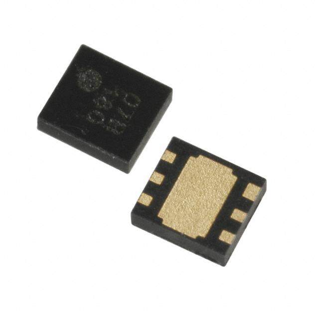
| 产品图片 |
|
| 产品型号 | LT1935ES5#TRMPBF |
| PWM类型 | 电流模式 |
| rohs | 无铅 / 符合限制有害物质指令(RoHS)规范要求 |
| 产品系列 | - |
| 产品目录页面 | |
| 供应商器件封装 | TSOT-23-5 |
| 其它名称 | LT1935ES5#PBF |
| 包装 | 带卷 (TR) |
| 同步整流器 | 无 |
| 安装类型 | 表面贴装 |
| 封装/外壳 | SOT-23-5 细型,TSOT-23-5 |
| 工作温度 | -40°C ~ 85°C |
| 标准包装 | 500 |
| 电压-输入 | 2.3 V ~ 16 V |
| 电压-输出 | 1.27 V ~ 38 V |
| 电流-输出 | 2A |
| 类型 | 升压(升压),回扫,Sepic |
| 输出数 | 1 |
| 输出类型 | 可调式 |
| 频率-开关 | 1.2MHz |


PDF Datasheet 数据手册内容提取
LT1935 1.2MHz Boost DC/DC Converter in ThinSOT with 2A Switch FEATURES DESCRIPTIOU ■ 1.2MHz Switching Frequency The LT®1935 is the industry’s highest power SOT-23 ■ High Output Voltage: Up to 38V switching regulator. Its unprecedented 2A, 40V internal ■ Wide Input Range: 2.3V to 16V switch allows high output currents to be generated in a ■ Low VCESAT Switch: 180mV at 2A small footprint. Intended for space-conscious applica- ■ Soft-Start tions, the LT1935 switches at 1.2MHz, allowing the use of ■ Uses Small Surface Mount Components tiny, low profile inductors and capacitors 2mm or less in ■ 5V at 1A from 3.3V Input height. The NPN switch achieves a V of just 180mV CESAT ■ 12V at 600mA from 5V Input at 2A independent of supply voltage, resulting in high ■ Low Shutdown Current: <1(cid:181)A efficiency even at maximum power levels from a 3V input. ■ Pin-for-Pin Compatible with the LT1613 and LT1930 A constant frequency, internally compensated, current ■ Low Profile (1mm) SOT-23 (ThinSOTTM) Package mode PWM architecture results in low, predictable output noise that is easy to filter. Low ESR ceramic capacitors can APPLICATIOU S be used on the output, further reducing noise to the millivolt level. The high voltage switch on the LT1935 is ■ Digital Cameras rated at 40V, making the device ideal for boost converters ■ Battery Backup up to 38V as well as for single-ended primary inductance ■ LCD Bias converter (SEPIC) and flyback designs. The device can ■ Local 5V or 12V Supply generate 5V at up to 1A from a 3.3V supply or 5V at 550mA ■ PC Cards from four alkaline cells in a SEPIC design. ■ xDSL Power Supply ■ TFT-LCD Bias Supply The LT1935 is available in a 5-lead SOT-23 package. , LTC and LT are registered trademarks of Linear Technology Corporation. ThinSOT is a trademark of Linear Technology Corporation. TYPICAL APPLICATIOU Efficiency, V = 12V OUT L1 90 VIN 4.2(cid:181)H D1 V12OVUT 85 VIN = 5V 5V 600mA 80 VIN = 3.3V 4.7(cid:181)F VIN SW 84.5k %) 75 LT1935 10(cid:181)F CY ( ON OFF SHDN FB EN 70 CI GND 10k EFFI 65 60 D1: ON SEMI MBRM120 L1: SUMIDA CDRH5D28-4R2 1935 F01 55 50 Figure 1. 5V to 12V, 600mA Step-Up DC/DC Converter 0 100 200 300 400 500 600 700 LOAD CURRENT (mA) 1935 F01b 1935f 1
LT1935 ABSOLUTE W AXIW UW RATIU GS PACKAGE/ORDER IU FORW ATIOU (Note 1) ORDER PART V Voltage .............................................................. 16V NUMBER IN TOP VIEW SW Voltage................................................–0.4V to 40V LT1935ES5 FB Voltage ................................................................. 6V SW 1 5 VIN GND 2 Current Into FB Pin.............................................. –1mA FB 3 4 SHDN SHDN Voltage......................................................... 16V S5 PART MARKING Maximum Junction Temperature......................... 125(cid:176)C S5 PACKAGE 5-LEAD PLASTIC TSOT-23 Operating Ambient Temperature Range LTRX TJMAX = 125(cid:176)C, θJA = 113(cid:176)C/W, (Note 2).............................................. –40(cid:176)C to 85(cid:176)C Storage Temperature Range................. –65(cid:176)C to 150(cid:176)C Strict adherence to JDEC 020B solder attach and rework Consult LTC marketing for parts specified with wider operating temperature ranges. for assemblies containing lead is recommended. ELECTRICAL CHARACTERISTICS The ● denotes specifications which apply over the full operating temperature range, otherwise specifications are TA = 25(cid:176)C. V = 3V, V = V unless otherwise noted. (Note 2) IN SHDN IN PARAMETER CONDITIONS MIN TYP MAX UNITS Feedback Voltage Measured at the FB Pin ● 1.240 1.265 1.280 V Feedback Voltage Line Regulation 2.5V ≤ VIN ≤ 16V 0.01 %/V FB Pin Bias Current V = V ● 12 60 nA FB REF Undervoltage Lockout Threshold 2.1 2.3 V Maximum Input Voltage 16 V Switching Frequency 1 1.2 1.4 MHz Maximum Duty Cycle ● 85 93 % Switch Current Limit (Note 3) 2 3.2 A Switch Saturating Voltage I = 2A 180 280 mV SW Switch Leakage Current VSW = 5V ● 0.01 1 (cid:181)A SHDN Pin Input Current VSHDN = 1.8V 14 40 (cid:181)A VSHDN = 0V 0.1 (cid:181)A Operating Supply Current V = 1.5V 3 mA FB SHDN Supply Current VSHDN = 0V 0.1 1 (cid:181)A SHDN Input High Voltage 1.8 V SHDN Input Low Voltage 0.5 V Note 1: Absolute Maximum Ratings are those values beyond which the life temperature range are assured by design, characterization and correlation of a device may be impaired. with statistical process controls. Note 2: The LT1935ES5 is guaranteed to meet performance specifications Note 3: Current limit guaranteed by design and/or correlation to static test. from 0(cid:176)C to 70(cid:176)C. Specifications over the –40(cid:176)C to 85(cid:176)C operating 1935f 2
LT1935 TYPICAL PERFORW AU CE CHARACTERISTICS FB Pin Voltage Oscillator Frequency Undervoltage Lockout 1.28 1.6 2.4 1.4 2.3 1.27 1.2 Hz) 2.2 M 1.0 V (V)FB1.26 QUENCY ( 00..86 UVLO (V) 2.1 E R 2.0 F 1.25 0.4 1.9 0.2 1.24 0 1.8 –50 –25 0 25 50 75 100 125 –50 –25 0 25 50 75 100 125 –50 –25 0 25 50 75 100 125 TEMPERATURE ((cid:176)C) TEMPERATURE ((cid:176)C) TEMPERATURE ((cid:176)C) 1935 G01 1935 G02 1935 G03 Peak Switch Current vs SHDN Pin Current Limit Switch Saturation Voltage Voltage (Soft-Start) 4 400 4 TA = 25(cid:176)C 50% DUTY CYCLE V) TA = 25(cid:176)C m 3 GE (300 3 NT LIMIT (A) 2 MIN TYP ATION VOLTA200 TA = 85(cid:176)C NT LIMIT (A) 2 URRE ATUR TA = 25(cid:176)C URRE C S C 1 H 100 1 C T WI S 0 0 0 0 20 40 60 80 100 0 0.5 1.0 1.5 2.0 2.5 3.0 0 0.5 1.0 1.5 2.0 DUTY CYCLE (%) SWITCH CURRENT (A) SHDN VOLTAGE (V) 1935 G04 1935 G05 1935 G06 SHDN Pin Current Frequency Foldback 80 1.4 TA = 25(cid:176)C TA = 25(cid:176)C 1.2 Hz) T (A)(cid:181) 60 CY (M 1.0 N N RE UE 0.8 R Q U 40 E C R SHDN PIN 20 WITCHING F 00..64 S 0.2 0 0 0 2 4 6 8 10 12 14 16 0 0.2 0.4 0.6 0.8 1.0 1.2 1.4 SHDN PIN VOLTAGE (V) FEEDBACK VOLTAGE (V) 1935 G07 1935 G08 1935f 3
LT1935 PIU FUU CTIOU S SW (Pin 1): Switch Pin. Connect inductor/diode here. SHDN (Pin 4): Shutdown Pin. Tie to 1.8V or more to enable Minimize trace area at this pin to reduce EMI. device. Ground to shut down. This pin also provides a soft- start function; see Applications Information section. GND (Pin 2): Ground. Tie directly to local ground plane. V (Pin 5): Input Supply Pin. Must be locally bypassed. FB (Pin 3): Feedback Pin. Reference voltage is 1.265V. IN Connect resistive divider tap here. Minimize trace area at FB. Set V according to V = 1.265V(1 + R1/R2). OUT OUT BLOCK DIAGRAW VIN 5 RE1F.E2R6E5NVCE + COMPARATOR 1 SW A1 – DRIVER FB 3 – RC A2 R Q Q1 + CC S SHDN 4 + Σ x15 0.01Ω – VOUT RAMP GENERATOR R1 (EXTERNAL) 2 GND FB 1.2MHz R2 (EXTERNAL) OSCILLATOR 1935 BD Figure 2. Block Diagram OPERATIOU The LT1935 uses a constant frequency, current mode is simply an amplified version of the difference between control scheme to provide excellent line and load regula- the feedback voltage and the reference voltage of 1.265V. tion. Operation can be best understood by referring to the In this manner, the error amplifier sets the correct peak Block Diagram in Figure 2. At the start of each oscillator current level to keep the output in regulation. If the error cycle, the SR latch is set, turning on the power switch Q1. amplifier’s output increases, more current is delivered to A voltage proportional to the switch current is added to a the output; if it decreases, less current is delivered. A stabilizing ramp and the resulting sum is fed into the clamp on the output of A1 (not shown) limits the switch positive terminal of the PWM comparator, A2. When this current to 3A. A1’s output is also clamped to the voltage voltage exceeds the level at the negative input of A2, the on the SHDN pin, providing a soft-start function by con- SR latch is reset, turning off the power switch. The level trolling the peak switch current during start-up. at the negative input of A2 is set by error amplifier A1, and 1935f 4
LT1935 APPLICATIOUNS INUFORWMATIOUN Inductor Selection Use a 4.7(cid:181)F ceramic capacitor to bypass the input of the LT1935. Be aware that the switching regulators require a Use inductors that are intended for high frequency power low impedance input supply. Additional bulk capacitance applications. The saturation current rating should be at may be required if the LT1935 circuit is more than a few least 2A. The RMS current rating, which is usually based inches away from the power source. If there are low ESR on heating of the inductor, should be higher than the capacitors nearby, the input bypass capacitor can be average current in the inductor in your application. For best efficiency, the DC resistance should be less than reduced to 2.2(cid:181)F. 100mΩ. The output capacitor supports the output under transient A good first choice for the inductor value results in a ripple loads and stabilizes the control loop of the LT1935. Look current that is 1/3 of the maximum switch current: at the typical application circuits as a starting point to choose a value. Generally, a higher output capacitance is L = 3 (V /V ) (V – V )/(I • f) IN OUT OUT IN MAX required at higher load currents and lower input voltages. I is the maximum switch current of 2A and f is the MAX Figure 3 shows transient response of the circuit in Fig- switching frequency. At lower duty cycles (less than 70%), ure1. The load is stepped from 200mA to 400mA and back this value can be lowered somewhat in order to use a to 200mA. The transient performance can be improved by physically smaller inductor. increasing the output capacitance, but may require a Table 1 lists several inductor manufacturers, along with phase lead capacitor between the output and the FB pin. part numbers for inductors that are a good match to the Figure 4 shows the transient response with the output LT1935. capacitor increased to 20(cid:181)F. Figure 5 shows the additional improvement resulting from the phase lead capacitor. Table 1. Inductor Suppliers Supplier Model Prefix Sumida CDRH4D18, CDRH4D28, CDRH5D18, CDRH5D28, CR43 VOUT Coiltronics/Cooper SD10, SD12, SD18, SD20 100mV/DIV .. Wurth Elektronik WE-PD2S, WE-PD3S, WE-PD4S Coilcraft MSS5131, MSS6132, DO1608 ILOAD 200mA/DIV Diode Selection 0 Use a Schottky rectifier with a 1A or higher current rating, such as the On Semiconductor MBRM120. Its 20V reverse 50(cid:181)s/DIV 1935 F03 Figure 3. Transient Response of the Circuit in Figure 1, voltage rating is adequate for most applications. Higher output voltages may require a 30V of 40V diode. COUT = 10(cid:181)F Capacitor Selection VOUT Use capacitors with low ESR (equivalent series resis- 100mV/DIV tance). In most cases, multilayer ceramic capacitors are the best choice. They offer high performance (very low ESR) in a small package. Use only X5R or X7R types; they ILOAD maintain their capacitance over temperature and applied 200mA/DIV voltage. Other suitable capacitor types include low-ESR tantalum capacitors that are specified for power applica- tions, and newer types of capacitors such as Sanyo’s 50(cid:181)s/DIV 1935 F04 POSCAP and Panasonic’s SP CAP. Figure 4. Transient Response with COUT = 20(cid:181)F 1935f 5
LT1935 APPLICATIOUNS INUFORWMATIOUN Soft Start The SHDN pin can be used to soft start the LT1935, VOUT 100mV/DIV reducing the maximum input current during start up. The SHDN pin is driven through an external RC filter to create a ramp at this pin. Figure 6 shows the start-up waveforms ILOAD 200mA/DIV with and without the soft start circuit. Without soft start, the input current peaks at ~3A. With soft start, the peak current is reduced to 1A. By choosing a large RC time 50(cid:181)s/DIV 1935 F05 constant, the peak start-up current can be reduced to the OUT 84.5k 68pF current that is required to regulate the output, with no overshoot. Choose the value of the resistor so that it can FB 20(cid:181)F supply 100(cid:181)A when the SHDN pin reaches 1.8V. 10k Figure 5. Transient Response with a 68pF Phase-Lead Capacitor RUN RUN 5V/DIV 5V/DIV VOUT VOUT 2V/DIV 2V/DIV IIN 1A/DIV IIN 1A/DIV 20(cid:181)s/DIV 1935 F06a 200(cid:181)s/DIV 1935 F06b 10k RUN SHDN RUN SHDN GND 0.22(cid:181)F GND Figure 6. Adding a Resistor and Capacitor to the SHDN Pin Reduces the Peak Input Current During Start-Up. V = 3.3V, IN VOUT = 5V, C2 = 20(cid:181)F, Output Load = 10Ω. Layout Hints The high speed operation of the LT1935 demands careful L1 D1 C1 attention to board layout. You will not get advertised + VOUT VIN performance with careless layout. Figure 7 shows the recommended component placement. Make the ground + C2 pin copper area large. This helps to lower the die SHDN R2 temperature. R1 C3 GND 1935 F03 Figure 7. Suggested Layout 1935f 6
LT1935 TYPICAL APPLICATIOU S Efficiency, V = 5V OUT 5V Boost Converter 90 L1 85 1.8(cid:181)H D1 VOUT VIN = 3.3V 2.3V TO 4V.8IVN 51VA, VIN = 3.3V 80 VIN = 2.5V C4.17(cid:181)F VINLT1935SW R291.4k C1530pF C20.6A, VIN = 2.5V CIENCY (%) 7750 ON OFF SHDN FB 20(cid:181)F EFFI 65 GND R2 60 10k 55 C1, C2: X5R OR X7R 6.3V D1: ON SEMI MBRM120 1935 TA01 50 L1: SUMIDA CR43-1R8 0 200 400 600 800 1000 1200 LOAD CURRENT (mA) 3.3V to 12V Boost Converter L1 VIN 4.2(cid:181)H D1 V12OVUT 3.3V 320mA C1 VIN SW 4.7(cid:181)F 47pF R1 LT1935 84.5k C2 ON OFF SHDN FB 22(cid:181)F GND R2 10k D1: ON SEMI MBRM120 L1: SUMIDA CDRH5D28-4R2 1935 TA02 PACKAGE DESCRIPTIOU S5 Package 5-Lead Plastic TSOT-23 (Reference LTC DWG # 05-08-1635) 0.62 0.95 MAX REF 2.90 BSC (NOTE 4) 1.22 REF 1.50 – 1.75 3.85 MAX2.62 REF 1.4 MIN 2.80 BSC (NOTE 4) PIN ONE RECOMMENDED SOLDER PAD LAYOUT 0.95 BSC 0.30 – 0.45 TYP PER IPC CALCULATOR 5 PLCS (NOTE 3) 0.80 – 0.90 0.20 BSC 0.01 – 0.10 1.00 MAX DATUM ‘A’ 0.30 – 0.50 REF 0.09 – 0.20 1.90 BSC NOTE: (NOTE 3) S5 TSOT-23 0302 1. DIMENSIONS ARE IN MILLIMETERS 4. DIMENSIONS ARE EXCLUSIVE OF MOLD FLASH AND METAL BURR 2. DRAWING NOT TO SCALE 5. MOLD FLASH SHALL NOT EXCEED 0.254mm 3. DIMENSIONS ARE INCLUSIVE OF PLATING 6. JEDEC PACKAGE REFERENCE IS MO-193 1935f Information furnished by Linear Technology Corporation is believed to be accurate and reliable. 7 However, no responsibility is assumed for its use. Linear Technology Corporation makes no represen- tation that the interconnection of its circuits as described herein will not infringe on existing patent rights.
LT1935 TYPICAL APPLICATIOU S 8V, 16V and –8V TFT LCD Power Supply 16V 10mA C5 D2B C3 L1 0.1(cid:181)F D2A 1(cid:181)F 2.2(cid:181)H VIN 8V 3.3V 450mA D1 C1 VIN SW R1 4.7(cid:181)F 100k LT1935 C2 ON OFF SHDN FB 10(cid:181)F GND R2 18.7k C1: X5R OR X7R 6.3V CC23,: CX45,R C O5R, C X67: RX 52R5V O R X7R 10V C0.61(cid:181)F D3A D3B C1(cid:181)4F D1: MBRM120 OR EQUIVALENT –8V D2, D3: BAT-54S OR EQUIVALENT 10mA L1: SUMIDA CDRH4D28-2R2 1935 TA03 5V SEPIC Converter C3 L1 VIN 4.7(cid:181)H 2.2(cid:181)F D1 VOUT 3.2V TO 9V 5V 425mA, VIN >3.2V C4.17(cid:181)F VIN SW R291.4k 47pF 550500mmAA,, VVIINN >>34.V6V LT1935 C2 ON OFF SHDN FB 47(cid:181)F L2 GND R2 4.7(cid:181)H 10k C1, C3: X5R OR X7R 10V D1: ON SEMI MBRM120 C2: X5R OR X7R 6.3V L1, L2: SUMIDA CDRH4D18-4R7 1935 TA04 RELATED PARTS PART NUMBER DESCRIPTION COMMENTS LT1618 1.5A (I ), 1.25MHz, High Efficiency Step-Up DC/DC Converter V : 1.6V to 18V, V : 35V, I : 1.8mA, SW IN OUT(MAX) Q ISD: <1(cid:181)A, MS, DFN Packages LT1930/LT1930A 1A (I ), 1.2MHz/2.2MHz, High Efficiency Step-Up DC/DC Converter V : 2.6V to 16V, V : 34V, I : 4.2mA/5.5mA SW IN OUT(MAX) Q ISD: <1(cid:181)A, ThinSOT Package LT1943 Quad Output, 2.6A Buck, 2.6A Boost, 0.3A Boost, V : 4.5V to 22V, V : 40V, I : 10mA, IN OUT(MAX) Q 0.4A Inverter 1.2MHz TFT DC/DC Converter ISD: <35(cid:181)A, TSSOP-28E Package LT1946/LT1946A 1.5A (I ), 1.2MHz/2.7MHz, High Efficiency Step-Up DC/DC Converter V : 2.45V to 16V, V : 34V, I : 3.2mA, SW IN OUT(MAX) Q ISD: <1(cid:181)A, MS8 Package LTC3400/LTC3400B 600mA (ISW), 1.2MHz, Synchronous Step-Up DC/DC Converter VIN: 0.85V to 5V, VOUT(MAX): 5V, IQ: 19(cid:181)A/300(cid:181)A ISD: <1(cid:181)A, ThinSOT Package LTC3401/LT3402 1A/2A(ISW), 3MHz, Synchronous Step-Up DC/DC Converter VIN: 0.5V to 5V, VOUT(MAX): 6V, IQ: 38(cid:181)A, ISD: <1(cid:181)A, MS Package LTC3425 5A (ISW), 8MHz, Multi-Phase Synchronous Step-Up DC/DC Converter VIN: 0.5V to 4.5V, VOUT(MAX): 5.25V, IQ: 12(cid:181)A, ISD: <1(cid:181)A, QFN Package LT3436 3A (I ), 1MHz, 34V Step-Up DC/DC Converter V : 3V to 25V, V : 34V, I : 0.9mA, SW IN OUT(MAX) Q ISD: <6(cid:181)A, TSSOP-16E Package LT3467/LT3467A 1.1A (I ), 1.3MHz/2.1MHz, High Efficiency Step-Up DC/DC Converter V : 2.6V to 16V, V : 40V, I : 1.2mA, SW IN OUT(MAX) Q ISD: <1(cid:181)A, ThinSOT Package 1935f 8 Linear Technology Corporation LT/TP 0604 1K (cid:149) PRINTED IN USA 1630 McCarthy Blvd., Milpitas, CA 95035-7417 (408) 432-1900 ● FAX: (408) 434-0507 ● www.linear.com ' LINEAR TECHNOLOGY CORPORATION 2004
Mouser Electronics Authorized Distributor Click to View Pricing, Inventory, Delivery & Lifecycle Information: A nalog Devices Inc.: LT1935ES5#TRMPBF LT1935ES5 LT1935ES5#PBF LT1935ES5#TR LT1935ES5#TRPBF LT1935ES5#TRM