ICGOO在线商城 > 集成电路(IC) > PMIC - 稳压器 - DC DC 开关稳压器 > LT1766IGN-5#PBF

 Datasheet下载
- 型号: LT1766IGN-5#PBF
- 制造商: LINEAR TECHNOLOGY
- 库位|库存: xxxx|xxxx
- 要求:
| 数量阶梯 | 香港交货 | 国内含税 |
| +xxxx | $xxxx | ¥xxxx |
查看当月历史价格
查看今年历史价格
LT1766IGN-5#PBF产品简介:
ICGOO电子元器件商城为您提供LT1766IGN-5#PBF由LINEAR TECHNOLOGY设计生产,在icgoo商城现货销售,并且可以通过原厂、代理商等渠道进行代购。 LT1766IGN-5#PBF价格参考。LINEAR TECHNOLOGYLT1766IGN-5#PBF封装/规格:PMIC - 稳压器 - DC DC 开关稳压器, 固定 降压,SEPIC 开关稳压器 IC 正 5V 1 输出 1.5A 16-SSOP(0.154",3.90mm 宽)。您可以下载LT1766IGN-5#PBF参考资料、Datasheet数据手册功能说明书,资料中有LT1766IGN-5#PBF 详细功能的应用电路图电压和使用方法及教程。
LT1766IGN-5#PBF 是由 Linear Technology(现已被 Analog Devices 收购)生产的一款 PMIC(电源管理集成电路),具体属于 DC-DC 开关稳压器类别。这款器件的主要应用场景包括但不限于以下几个方面:

 1. 工业自动化与控制
   LT1766IGN-5#PBF 可用于工业自动化系统中的电源管理,例如 PLC(可编程逻辑控制器)、传感器接口和执行器驱动电路等。它能够为这些设备提供稳定的电源输出,确保系统在复杂电磁环境下稳定运行。

 2. 通信设备
   在通信基站、路由器、交换机等设备中,该芯片可以作为高效电源转换器,将输入电压转换为所需的输出电压,以满足不同模块的供电需求。其高效率和低噪声特性有助于提高通信系统的可靠性和性能。

 3. 医疗设备
   医疗设备如监护仪、超声波设备、便携式医疗仪器等对电源的稳定性和可靠性要求极高。LT1766IGN-5#PBF 能够提供精确的电压调节,并且具备良好的瞬态响应能力,适用于这些对精度和稳定性有严格要求的应用场景。

 4. 汽车电子
   汽车电子系统中的电源管理至关重要,尤其是在现代电动汽车和混合动力汽车中。LT1766IGN-5#PBF 可用于车载信息娱乐系统、导航系统、电池管理系统等,确保这些系统在车辆启动、怠速或行驶过程中都能获得稳定的电源供应。

 5. 消费电子产品
   在一些高性能消费电子产品中,如笔记本电脑、平板电脑、智能手表等,该芯片可以用于内部电源管理,确保各个功能模块(如处理器、显示屏、无线模块等)得到合适的供电电压,同时延长电池寿命。

 6. 测试与测量仪器
   测试与测量仪器如示波器、万用表、信号发生器等需要非常稳定的电源来保证测量精度。LT1766IGN-5#PBF 的高精度输出电压和低纹波特性使其成为这些应用的理想选择。

总之,LT1766IGN-5#PBF 凭借其高效、稳定、低噪声的特点,在多个领域有着广泛的应用,尤其适合对电源质量和可靠性要求较高的场合。
| 参数 | 数值 |
| 产品目录 | 集成电路 (IC) |
| 描述 | IC REG BUCK 5V 1.5A 16SSOP |
| 产品分类 | |
| 品牌 | Linear Technology |
| 数据手册 | |
| 产品图片 |
|
| 产品型号 | LT1766IGN-5#PBF |
| PWM类型 | 电流模式 |
| rohs | 无铅 / 符合限制有害物质指令(RoHS)规范要求 |
| 产品系列 | - |
| 供应商器件封装 | 16-SSOP |
| 其它名称 | LT1766IGN5PBF |
| 包装 | 管件 |
| 同步整流器 | 无 |
| 安装类型 | 表面贴装 |
| 封装/外壳 | 16-SSOP(0.154",3.90mm 宽) |
| 工作温度 | -40°C ~ 125°C |
| 标准包装 | 100 |
| 电压-输入 | 5.5 V ~ 60 V |
| 电压-输出 | 5V |
| 电流-输出 | 1.5A |
| 类型 | 降压(降压) |
| 输出数 | 1 |
| 输出类型 | 固定 |
| 频率-开关 | 200kHz |


- 商务部:美国ITC正式对集成电路等产品启动337调查
- 曝三星4nm工艺存在良率问题 高通将骁龙8 Gen1或转产台积电
- 太阳诱电将投资9.5亿元在常州建新厂生产MLCC 预计2023年完工
- 英特尔发布欧洲新工厂建设计划 深化IDM 2.0 战略
- 台积电先进制程称霸业界 有大客户加持明年业绩稳了
- 达到5530亿美元!SIA预计今年全球半导体销售额将创下新高
- 英特尔拟将自动驾驶子公司Mobileye上市 估值或超500亿美元
- 三星加码芯片和SET,合并消费电子和移动部门,撤换高东真等 CEO
- 三星电子宣布重大人事变动 还合并消费电子和移动部门
- 海关总署:前11个月进口集成电路产品价值2.52万亿元 增长14.8%


PDF Datasheet 数据手册内容提取
LT1766/LT1766-5 5.5V to 60V 1.5A, 200kHz Step-Down Switching Regulator FEATURES DESCRIPTION n Wide Input Range: 5.5V to 60V The LT®1766/LT1766-5 are 200kHz monolithic buck switch- n 1.5A Peak Switch Current ing regulators that accept input voltages up to 60V. A high n Constant 200kHz Switching Frequency effi ciency 1.5A, 0.2Ω switch is included on the die along n Saturating Switch Design: 0.2Ω with all the necessary oscillator, control and logic circuitry. n Peak Switch Current Rating Maintained Over A current mode control architecture delivers fast transient Full Duty Cycle Range response and excellent loop stability. n Low Effective Supply Current: 2.5mA Special design techniques and a new high voltage process n Low Shutdown Current: 25μA achieve high effi ciency over a wide input range. Effi ciency n 1.2V Feedback Reference Voltage (LT1766) is maintained over a wide output current range by using the n 5V Fixed Output (LT1766-5) output to bias the circuitry and by utilizing a supply boost n Easily Synchronizable capacitor to saturate the power switch. Patented circuitry n Cycle-by-Cycle Current Limiting maintains peak switch current over the full duty cycle range. n Small 16-Pin SSOP and Thermally Enhanced A shutdown pin reduces supply current to 25μA and the TSSOP Packages device can be externally synchronized from 228kHz to APPLICATIONS 700kHz with logic-level inputs. The LT1766/LT1766-5 are available in a 16-pin fused-lead n High Voltage, Industrial and Automotive SSOP package or a TSSOP package with exposed backside n Portable Computers for improved thermal performance. n Battery-Powered Systems n Battery Chargers L, LT, LTC, LTM, Linear Technology and the Linear logo are registered trademarks and ThinSOT is a trademark of Linear Technology Corporation. All other trademarks are the property n Distributed Power Systems of their respective owners. Protected by U.S. Patents, including 6498466, 6531909. TYPICAL APPLICATION 5V Buck Converter 1N4148W Effi ciency vs Load Current 6 0.33μF 100 5.5V TOV 6I0NV* 2.2μF† 4 VIN BOOST SW 2 47μH V51VAOUT 90 VL O=U 4T7 =μ H5V VIN = 12V 1C0E0RVAMIC LT1766 10MQ060N + 100μF 10V OFF ON 15 SHDN BIAS 10 STAONLITDALUM Y (%) 80 VIN = 42V 15.4k NC 14 12 E SYNC FB CI FI 70 F GND VC 4.99k E 1, 8, 9, 16 11 60 2.2k 220pF 50 0.022μF 0 0.25 0.50 0.75 1.00 1.25 LOAD CURRENT (A) 1766 TA01 1766 TA02 *FOR INPUT VOLTAGES BELOW 7.5V, SOME RESTRICTIONS MAY APPLY †TDK C4532X7R2A225K 1766fc 1
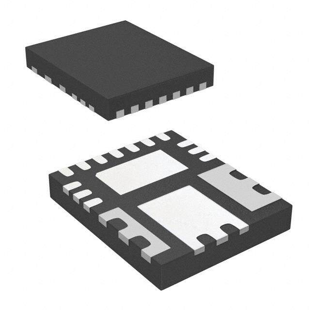
LT1766/LT1766-5 ABSOLUTE MAXIMUM RATINGS (Note 1) Input Voltage (V ) .................................................. 60V Operating Junction Temperature Range IN BOOST Pin Above SW .............................................. 35V LT1766EFE/LT1766EFE-5/LT1766EGN/ BOOST Pin Voltage ................................................. 68V LT1766EGN-5 (Note 8,10) ....................–40°C to 125°C SYNC, SENSE Voltage (LT1766-5) ............................. 7V LT1766IFE/LT1766IFE-5/ SHDN Voltage ............................................................ 6V LT1766IGN/LT1766IGN-5 (Note 8,10) ..–40°C to 125°C BIAS Pin Voltage ..................................................... 30V LT1766HFE ..........................................–40°C to 140°C FB Pin Voltage/Current (LT1766) ................... 3.5V/2mA Storage Temperature Range ..................–65°C to 150°C Lead Temperature (Soldering, 10 sec) ..................300°C PIN CONFIGURATION TOP VIEW TOP VIEW GND 1 16 GND GND 1 16 GND SW 2 15 SHDN SW 2 15 SHDN NC 3 14 SYNC NC 3 14 SYNC VIN 4 17 13 NC VIN 4 13 NC NC 5 GND 12 FB/SENSE NC 5 12 FB/SENSE BOOST 6 11 VC BOOST 6 11 VC NC 7 10 BIAS NC 7 10 BIAS GND 8 9 GND GND 8 9 GND FE PACKAGE GN PACKAGE 16-LEAD PLASTIC TSSOP 16-LEAD PLASTIC SSOP θJA = 45°C, θJC (PIN 17) = 10°C/W θJA = 85°C, θJC (PIN 8) = 25°C/W EXPOSED PAD (PIN 17) IS GND, MUST BE SOLDERED TO PCB FOUR CORNER PINS SOLDERED TO GROUND PIN 1766fc 2
LT1766/LT1766-5 ORDER INFORMATION LEAD FREE FINISH TAPE AND REEL PART MARKING PACKAGE DESCRIPTION TEMPERATURE RANGE LT1766EFE#PBF LT1766EFE#TRPBF 1766EFE 16-Lead Plastic TSSOP 0°C to 125°C LT1766IFE#PBF LT1766IFE#TRPBF 1766IFE 16-Lead Plastic TSSOP –40°C to 125°C LT1766HFE#PBF LT1766HFE#TRPBF 1766HFE 16-Lead Plastic TSSOP –40°C to 140°C LT1766EFE-5#PBF LT1766EFE-5#TRPBF 1766EFE-5 16-Lead Plastic TSSOP 0°C to 125°C LT1766IFE-5#PBF LT1766IFE-5#TRPBF 1766IFE-5 16-Lead Plastic TSSOP –40°C to 125°C LT1766EGN#PBF LT1766EGN#TRPBF 1766 16-Lead Plastic SSOP 0°C to 125°C LT1766IGN#PBF LT1766IGN#TRPBF 1766I 16-Lead Plastic SSOP –40°C to 125°C LT1766EGN-5#PBF LT1766EGN-5#TRPBF 17665 16-Lead Plastic SSOP 0°C to 125°C LT1766IGN-5#PBF LT1766IGN-5#TRPBF 1766I5 16-Lead Plastic SSOP –40°C to 125°C LEAD BASED FINISH TAPE AND REEL PART MARKING PACKAGE DESCRIPTION TEMPERATURE RANGE LT1766EFE LT1766EFE#TR 1766EFE 16-Lead Plastic TSSOP 0°C to 125°C LT1766IFE LT1766IFE#TR 1766IFE 16-Lead Plastic TSSOP –40°C to 85°C LT1766HFE LT1766HFE#TR 1766HFE 16-Lead Plastic TSSOP –40°C to 140°C LT1766EFE-5 LT1766EFE-5#TR 1766EFE-5 16-Lead Plastic TSSOP 0°C to 125°C LT1766IFE-5 LT1766IFE-5#TR 1766IFE-5 16-Lead Plastic TSSOP –40°C to 125°C LT1766EGN LT1766EGN#TR 1766 16-Lead Plastic SSOP 0°C to 125°C LT1766IGN LT1766IGN#TR 1766I 16-Lead Plastic SSOP –40°C to 125°C LT1766EGN-5 LT1766EGN-5#TR 17665 16-Lead Plastic SSOP 0°C to 125°C LT1766IGN-5 LT1766IGN-5#TR 1766I5 16-Lead Plastic SSOP –40°C to 125°C Consult LTC Marketing for parts specifi ed with wider operating temperature ranges. For more information on lead free part marking, go to: http://www.linear.com/leadfree/ For more information on tape and reel specifi cations, go to: http://www.linear.com/tapeandreel/ ELECTRICAL CHARACTERISTICS (LT1766E/LT1766I Grade) The l denotes specifi cations which apply over the full operating temperature range, otherwise specifi cations are at T = 25°C. J V = 15V, VC = 1.5V, SHDN = 1V, BOOST open circuit, SW open circuit, unless otherwise noted. IN PARAMETER CONDITIONS MIN TYP MAX UNITS Reference Voltage (V ) (LT1766) 5.5V ≤ V ≤ 60V 1.204 1.219 1.234 V REF IN V + 0.2 ≤ V ≤ V – 0.2 l 1.195 1.243 V OL C OH SENSE Voltage (LT1766-5) 5.5V ≤ V ≤ 60V 4.94 5 5.06 V IN V + 0.2V ≤ V ≤ V – 0.2V l 4.90 5.10 V OL C OH SENSE Pin Resistance (LT1766-5) 9.5 13.8 19 kΩ FB Input Bias Current (LT1766) l –0.5 –1.5 μA Error Amp Voltage Gain (Notes 2, 9) 200 400 V/V Error Amp g dl (V ) = ±10μA (Note 9) 1500 2000 3000 μMho m C l 1000 4200 μMho V to Switch g 1.7 A/V C m EA Source Current FB = 1V or V = 4.1V l 125 225 400 μA SENSE EA Sink Current FB = 1.4V or V = 5.7V l 100 225 450 μA SENSE V Switching Threshold Duty Cycle = 0 0.9 V C V High Clamp SHDN = 1V 2.1 V C Switch Current Limit V Open, Boost = V + 5V, FB = 1V or V = 4.1V l 1.5 2 3 A C IN SENSE 1766fc 3
LT1766/LT1766-5 ELECTRICAL CHARACTERISTICS (LT1766E/LT1766I Grade) The l denotes specifi cations which apply over the full operating temperature range, otherwise specifi cations are at T = 25°C. J V = 15V, V = 1.5V, SHDN = 1V, BOOST open circuit, SW open circuit, unless otherwise noted. IN C PARAMETER CONDITIONS MIN TYP MAX UNITS Switch On-Resistance I = 1.5A, Boost = V + 5V (Note 7) 0.2 0.3 Ω SW IN l 0.4 Ω Maximum Switch Duty Cycle FB = 1V or V = 4.1V 93 96 % SENSE l 90 % Switch Frequency V Set to Give DC = 50% 184 200 216 kHz C l 172 200 228 kHz f Line Regulation 5.5V ≤ V ≤ 60V l 0.05 0.15 %/V SW IN f Frequency Shifting Threshold Df = 10kHz 0.8 V SW Minimum Input Voltage (Note 3) l 4.6 5.5 V Minimum Boost Voltage (Note 4) I ≤ 1.5A l 1.8 3 V SW Boost Current (Note 5) Boost = V + 5V, I = 0.5A l 12 25 mA IN SW Boost = V + 5V, I = 1.5A l 45 70 mA IN SW Input Supply Current (I ) (Note 6) V = 5V 1.4 2.2 mA VIN BIAS Bias Supply Current (I ) (Note 6) V = 5V 2.9 4.2 mA BIAS BIAS Shutdown Supply Current SHDN = 0V, V ≤ 60V, SW = 0V, V Open 25 75 μA IN C l 200 μA Lockout Threshold V Open l 2.3 2.42 2.53 V C Shutdown Thresholds V Open, Shutting Down l 0.15 0.37 0.6 V C V Open, Starting Up l 0.25 0.45 0.6 V C Minimum SYNC Amplitude l 1.5 2.2 V SYNC Frequency Range 228 700 kHz SYNC Input Resistance 20 kΩ (LT1766H Grade) The l denotes specifi cations which apply over the full operating temperature range, otherwise specifi cations are at T = 25°C. J V = 15V, V = 1.5V, SHDN = 1V, BOOST open circuit, SW open circuit, unless otherwise noted. IN C PARAMETER CONDITIONS MIN TYP MAX UNITS Reference Voltage (V ) 5.5V ≤ V ≤ 60V 1.204 1.219 1.234 V REF IN V + 0.2 ≤ V ≤ V – 0.2 l 1.175 1.265 V OL C OH FB Input Bias Current l –0.5 –1.5 μA Error Amp Voltage Gain (Notes 2, 9) 200 400 V/V Error Amp g dl (V ) = ±10μA (Note 9) 1500 2000 3000 μMho m C l 900 4200 μMho V to Switch g 1.7 A/V C m EA Source Current FB = 1V or V = 4.1V l 125 225 400 μA SENSE EA Sink Current FB = 1.4V or V = 5.7V l 100 225 450 μA SENSE V Switching Threshold Duty Cycle = 0 0.9 V C V High Clamp SHDN = 1V 2.1 V C Switch Current Limit V Open, Boost = V + 5V, FB = 1V or V = 4.1V l 0.75 2 3 A C IN SENSE Switch On Resistance I = 0.75A, Boost = V + 5V (Note 7) 0.2 0.3 Ω SW IN l 0.8 Ω Maximum Switch Duty Cycle FB = 1V or V = 4.1V 93 96 % SENSE l 90 % Switch Frequency V Set to Give DC = 50% 184 200 216 kHz C l 135 200 228 kHz 1766fc 4
LT1766/LT1766-5 ELECTRICAL CHARACTERISTICS (LT1766H Grade) The l denotes specifi cations which apply over the full operating temperature range, otherwise specifi cations are at T = 25°C. J V = 15V, V = 1.5V, SHDN = 1V, BOOST open circuit, SW open circuit, unless otherwise noted. IN C PARAMETER CONDITIONS MIN TYP MAX UNITS f Line Regulation 5.5V ≤ V ≤ 60V l 0.05 0.15 %/V SW IN f Frequency Shifting Threshold Df = 10kHz 0.8 V SW Minimum Input Voltage (Note 3) l 4.6 5.5 V Minimum Boost Voltage (Note 4) I ≤ 0.75A l 1.8 3 V SW Boost Current (Note 5) Boost = V + 5V, I = 0.5A l 12 40 mA IN SW Boost = V + 5V, I = 0.75A l 45 100 mA IN SW Input Supply Current (I ) (Note 6) V = 5V 1.4 2.2 mA VIN BIAS Bias Supply Current (I ) (Note 6) V = 5V 2.9 4.2 mA BIAS BIAS Shutdown Supply Current SHDN = 0V, V ≤ 60V, SW = 0V, V Open 25 120 μA IN C l 500 μA Lockout Threshold V Open l 2.3 2.42 2.68 V C Shutdown Thresholds V Open, Shutting Down l 0.15 0.37 0.9 V C V Open, Starting Up l 0.25 0.45 0.9 V C Minimum SYNC Amplitude l 1.5 2.2 V SYNC Frequency Range 228 700 kHz SYNC Input Resistance 20 kΩ Note 1: Stresses beyond those listed under Absolute Maximum Ratings Note 7: Switch on-resistance is calculated by dividing V to SW voltage IN may cause permanent damage to the device. Exposure to any Absolute by the forced current. See Typical Performance Characteristics for the Maximum Rating condition for extended periods may affect device graph of switch voltage at other currents. reliability and lifetime. Note 8: The LT1766EGN, LT1766EGN-5, LT1766EFE and LT1766EFE-5 Note 2: Gain is measured with a V swing equal to 200mV above the low are guaranteed to meet performance specifi cations from 0°C to 125°C C clamp level to 200mV below the upper clamp level. junction temperature. Specifi cations over the –40°C to 125°C operating Note 3: Minimum input voltage is not measured directly, but is guaranteed junction temperature range are assured by design, characterization and by other tests. It is defi ned as the voltage where internal bias lines are still correlation with statistical process controls. The LT1766IGN, LT1766IGN-5, regulated so that the reference voltage and oscillator remain constant. LT1766IFE and LT1766IFE-5 are guaranteed over the full –40°C to 125°C Actual minimum input voltage to maintain a regulated output will depend operating junction temperature range. The LT1766HGN and LT1766HFE are upon output voltage and load current. See Applications Information. guaranteed over the full –40°C to 140°C operating junction temperature range. Note 4: This is the minimum voltage across the boost capacitor needed to guarantee full saturation of the internal power switch. Note 9: Transconductance and voltage gain refer to the internal amplifi er exclusive of the voltage divider. To calculate gain and transconductance, Note 5: Boost current is the current fl owing into the BOOST pin with the refer to the SENSE pin on fi xed voltage parts. Divide the values shown by pin held 5V above input voltage. It fl ows only during switch on time. the ratio V /1.219. Note 6: Input supply current is the quiescent current drawn by the input OUT Note 10: This IC includes overtemperature protection that is intended pin when the BIAS pin is held at 5V with switching disabled. Bias supply to protect the device during momentary overload conditions. Junction current is the current drawn by the BIAS pin when the BIAS pin is held temperature will exceed 140°C when overtemperature protection is active. at 5V. Total input referred supply current is calculated by summing input Continuous operation above the specifi ed maximum operating junction supply current (I ) with a fraction of bias supply current (I ): VIN BIAS temperature may impair device reliability. I = I + (I )(V /V ) TOTAL VIN BIAS OUT IN Note 11: High junction temperatures degrade operating lifetimes. with V = 15V, V = 5V, I = 1.4mA, I = 2.9mA, I = 2.4mA. IN OUT VIN BIAS TOTAL Operating lifetime at junction temperatures between 125°C and 140°C is derated to 1000 hours. 1766fc 5
LT1766/LT1766-5 TYPICAL PERFORMANCE CHARACTERISTICS Switch Peak Current Limit FB Pin Voltage and Current SHDN Pin Bias Current 2.5 1.234 2.0 250 TA = 25°C CURRENT REQUIRED TO FORCE SHUTDOWN 1.229 200 (FLOWS OUT OF PIN). AFTER SHUTDOWN, WITCH PEAK CURRENT (A) 12..50 GUARANTTYEPEIDC AMLINIMUM FEEDBACK VOLTAGE (V) 111...222112494 CVUORLTRAEGNET 011...550 CURRENT (μA) CURRENT (μA) 11501002 CURRAETN 2T.3 D8RVO SPTSA NTOD BAY F TEHWR μEASHOLD S (CURRENT FLOWS OUT OF PIN) 1.209 6 1.0 1.204 0 0 0 20 40 60 80 100 –50 –25 0 25 50 75 100 125 150 –50 –25 0 25 50 75 100 125 150 DUTY CYCLE (%) JUNCTION TEMPERATURE (°C) JUNCTION TEMPERATURE (°C) 1766 G01 1766 G02 1766 G03 Lockout and Shutdown Thresholds Shutdown Supply Current Shutdown Supply Current 2.4 40 300 VSHDN = 0V TA = 25°C LOCKOUT 35 TA = 25°C 2.0 A) A)250 VOLTAGE (V) 11..62 Y CURRENT (μ 322050 Y CURRENT (μ125000 VIN = 60V VIN = 15V HDN PIN 0.8 T SUPPL 15 T SUPPL100 S START-UP NPU 10 NPU 0.4 I I 50 5 SHUTDOWN 0 0 0 –50 –25 0 25 50 75 100 125 150 0 10 20 30 40 50 60 0 0.1 0.2 0.3 0.4 0.5 JUNCTION TEMPERATURE (°C) INPUT VOLTAGE (V) SHUTDOWN VOLTAGE (V) 1766 G04 1766 G05 1766 G06 Error Amplifi er Transconductance Error Amplifi er Transconductance Frequency Foldback 2500 3000 200 600 TA = 25°C TA = 25°C μmho)2000 2500 PHASE 150 Y (kHz)A)500 TRANSCONDUCTANCE (11505000000 GAIN (μMho)211050000000 EVRFRB(O2R • A10M–3PG)LAIFINIER EQUIR2V0OA0ULkTENT CIRC1C2OUpUIVTFTC 150000PHASE (DEG) SWITICHING FREQUENCOR FB CURRENT (μ142300000000 FSRWEIQTUCEHNINCGY FB PIN RLOAD = 50Ω CURRENT 0 500 –50 0 –50 –25 0 25 50 75 100 125 150 100 1k 10k 100k 1M 10M 0 0.5 1.0 1.5 JUNCTION TEMPERATURE (°C) FREQUENCY (Hz) VFB (V) 1766 G08 1766 G07 1766 G09 1766fc 6
LT1766/LT1766-5 TYPICAL PERFORMANCE CHARACTERISTICS Minimum Input Voltage with 5V Switching Frequency Output BOOST Pin Current 230 7.5 45 TA = 25°C TA = 25°C 40 220 7.0 A) 35 m FREQUENCY (kHz) 221109000 NPUT VOLTAGE (V) 66..50 MVOINLITMAUGME T ION PSUTTART ST PIN CURRENT ( 32210505 I O O 5.5 MINIMUM INPUT B 10 180 VOLTAGE TO RUN 5 170 5.0 0 –50 –25 0 25 50 75 100 125 150 0 0.1 0.2 0.3 0.4 0.5 0.6 0.7 0.8 0.9 1 0 0.5 1 1.5 JUNCTION TEMPERATURE (°C) LOAD CURRENT (A) SWITCH CURRENT (A) 1766 G10 1766 G11 1766 G12 Switch Minimum On-Time V Pin Shutdown Threshold Switch Voltage Drop vs Temperature C 2.1 450 600 400 1.9 TJ = 150°C ns) 500 THRESHOLD VOLTAGE (V) 1111....5317 SWITCH VOLTAGE (mV) 332211505050000000 TJ T=J 2=5 1°C25°C TJ = –40°C WITCH MINIMUM ON TIME ( 234000000 0.9 S 100 50 0.7 0 0 –50 –25 0 25 50 75 100 125 150 0 0.5 1 1.5 –50 –25 0 25 50 75 100 125 150 JUNCTION TEMPERATURE (°C) SWITCH CURRENT (A) JUNCTION TEMPERATURE (°C) 1766 G13 1766 G14 1766 G15 PIN FUNCTIONS GND (Pins 1, 8, 9, 16, 17): The GND pin connections act copper ground plane underneath the device. (See Applica- as the reference for the regulated output, so load regula- tions Information—Layout Considerations.) tion will suffer if the ground end of the load is not at the SW (Pin 2): The switch pin is the emitter of the on-chip same voltage as the GND pins of the IC. This condition will power NPN switch. This pin is driven up to the input pin occur when load current or other currents fl ow through voltage during switch on-time. Inductor current drives the metal paths between the GND pins and the load ground. switch pin negative during switch off-time. Negative volt- Keep the paths between the GND pins and the load ground age is clamped with the external catch diode. Maximum short and use a ground plane when possible. The GND negative switch voltage allowed is –0.8V. pin also acts as a heat sink and should be soldered to a large copper plane to reduce thermal resistance. For the NC (Pins 3, 5, 7, 13): No Connection. FE package, the exposed pad should be soldered to the 1766fc 7
LT1766/LT1766-5 PIN FUNCTIONS V (Pin 4): This is the collector of the on-chip power NPN FB/SENSE (Pin 12): The feedback pin is used to set the IN switch. V powers the internal control circuitry when a output voltage using an external voltage divider that gener- IN voltage on the BIAS pin is not present. High dI/dt edges ates 1.22V at the pin for the desired output voltage. The occur on this pin during switch turn on and off. Keep 5V fi xed output voltage parts have the divider included on the path short from the V pin through the input bypass the chip and the FB pin is used as a SENSE pin, connected IN capacitor, through the catch diode back to SW. All trace directly to the 5V output. Three additional functions are inductance on this path will create a voltage spike at switch performed by the FB pin. When the pin voltage drops below off, adding to the V voltage across the internal NPN. 0.6V, switch current limit is reduced and the external SYNC CE function is disabled. Below 0.8V, switching frequency is BOOST (Pin 6): The BOOST pin is used to provide a drive also reduced. See Feedback Pin Functions in Applications voltage, higher than the input voltage, to the internal bipolar Information for details. NPN power switch. Without this added voltage, the typical switch voltage loss would be about 1.5V. The additional SYNC (Pin 14): The SYNC pin is used to synchronize the BOOST voltage allows the switch to saturate and voltage internal oscillator to an external signal. It is directly logic loss approximates that of a 0.2Ω FET structure, but with compatible and can be driven with any signal between 10% much smaller die area. and 90% duty cycle. The synchronizing range is equal to initial operating frequency up to 700kHz. See Synchroniz- BIAS (Pin 10): The BIAS pin is used to improve effi ciency ing in Applications Information for details. when operating at higher input voltages and light load cur- rent. Connecting this pin to the regulated output voltage SHDN (Pin 15): The SHDN pin is used to turn off the forces most of the internal circuitry to draw its operating regulator and to reduce input drain current to a few mi- current from the output voltage rather than the input supply. croamperes. This pin has two thresholds: one at 2.38V to This architecture increases effi ciency especially when the disable switching and a second at 0.4V to force complete input voltage is much higher than the output. Minimum micropower shutdown. The 2.38V threshold functions output voltage setting for this mode of operation is 3V. as an accurate undervoltage lockout (UVLO); sometimes used to prevent the regulator from delivering power until V (Pin 11) The V pin is the output of the error amplifi er C C the input voltage has reached a predetermined level. and the input of the peak switch current comparator. It is normally used for frequency compensation, but can also If the SHDN pin functions are not required, the pin can serve as a current clamp or control loop override. V sits either be left open (to allow an internal bias current to lift C at about 0.9V for light loads and 2.1V at maximum load. the pin to a default high state) or be forced high to a level It can be driven to ground to shut off the regulator, but if not to exceed 6V. driven high, current must be limited to 4mA. BLOCK DIAGRAM The LT1766 is a constant frequency, current mode buck the comparator, the fl ip-fl op is reset and the switch turns converter. This means that there is an internal clock and off. Output voltage control is obtained by using the output two feedback loops that control the duty cycle of the power of the error amplifi er to set the switch current trip point. switch. In addition to the normal error amplifi er, there is a This technique means that the error amplifi er commands current sense amplifi er that monitors switch current on a current to be delivered to the output rather than voltage. cycle-by-cycle basis. A switch cycle starts with an oscillator A voltage fed system will have low phase shift up to the pulse which sets the R fl ip-fl op to turn the switch on. When resonant frequency of the inductor and output capacitor, S switch current reaches a level set by the inverting input of then an abrupt 180° shift will occur. The current fed system 1766fc 8
LT1766/LT1766-5 BLOCK DIAGRAM will have 90° phase shift at a much lower frequency, but output voltage). This will improve effi ciency if the BIAS will not have the additional 90° shift until well beyond pin voltage is lower than regulator input voltage. the LC resonant frequency. This makes it much easier to High switch effi ciency is attained by using the BOOST frequency compensate the feedback loop and also gives pin to provide a voltage to the switch driver which is much quicker transient response. higher than the input voltage, allowing switch to be satu- Most of the circuitry of the LT1766 operates from an internal rated. This boosted voltage is generated with an external 2.9V bias line. The bias regulator normally draws power capacitor and diode. Two comparators are connected to the from the regulator input pin, but if the BIAS pin is connected shutdown pin. One has a 2.38V threshold for undervoltage to an external voltage higher than 3V, bias power will be lockout and the second has a 0.4V threshold for complete drawn from the external source (typically the regulated shutdown. VIN 4 RLIMIT RSENSE 2.9V BIAS INTERNAL + – BIAS 10 REGULATOR VCC CURRENT COMPARATOR SLOPE COMP ∑ SYNC 14 ANTISLOPE COMP BOOST 6 SHUTDOWN COMPARATOR 200kHz + – OSCILLATOR S RS DRIVER QPO1WER FLIP-FLOP CIRCUITRY SWITCH R 0.4V 5.5μA 2 SW SHDN 15 + FREQUENCY – FOLDBACK LOCKOUT COMPARATOR ×1 Q2 FOLDBACK VC(MAX) Q3 CURRENT CLAMP LIMIT ERROR CLAMP AMPLIFIER – gm = 2000μMho 12 FB + 11 2.38V 1.22V VC GND 1, 8, 9, 16, 17 1766 F01 Figure 1. LT1766 Block Diagram 1766fc 9
LT1766/LT1766-5 APPLICATIONS INFORMATION FEEDBACK PIN FUNCTIONS regulator to operate at very low duty cycles, and the average current through the diode and inductor is equal The feedback (FB) pin on the LT1766 is used to set output to the short-circuit current limit of the switch (typically 2A voltage and provide several overload protection features. for the LT1766, folding back to less than 1A). Minimum The fi rst part of this section deals with selecting resistors switch on-time limitations would prevent the switcher to set output voltage and the remaining part talks about from attaining a suffi ciently low duty cycle if switching foldback frequency and current limiting created by the FB frequency were maintained at 200kHz, so frequency is pin. Please read both parts before committing to a fi nal reduced by about 5:1 when the feedback pin voltage drops design. The 5V fi xed output voltage part (LT1766-5) has below 0.8V (see Frequency Foldback graph). This does internal divider resistors and the FB pin is renamed SENSE, not affect operation with normal load conditions; one connected directly to the output. simply sees a gear shift in switching frequency during The suggested value for the output divider resistor (see start-up as the output voltage rises. Figure 2) from FB to ground (R2) is 5k or less, and a In addition to lower switching frequency, the LT1766 also formula for R1 is shown below. The output voltage error operates at lower switch current limit when the feedback caused by ignoring the input bias current on the FB pin pin voltage drops below 0.6V. Q2 in Figure 2 performs is less than 0.25% with R2 = 5k. A table of standard 1% this function by clamping the V pin to a voltage less than values is shown in Table 1 for common output voltages. C its normal 2.1V upper clamp level. This foldback current Please read the following if divider resistors are increased limit greatly reduces power dissipation in the IC, diode above the suggested values. and inductor during short-circuit conditions. External syn- ( ) R1= R2 VOUT −1.22 chronization is also disabled to prevent interference with 1.22 foldback operation. Again, it is nearly transparent to the user under normal load conditions. The only loads that may be Table 1 affected are current source loads which maintain full load OUTPUT R1 % ERROR AT OUTPUT current with output voltage less than 50% of fi nal value. VOLTAGE R2 (NEAREST 1%) DUE TO DISCREET 1% In these rare situations the feedback pin can be clamped (V) (kΩ) (kΩ) RESISTOR STEPS above 0.6V with an external diode to defeat foldback cur- 3 4.99 7.32 +0.32 rent limit. Caution: clamping the feedback pin means that 3.3 4.99 8.45 –0.43 frequency shifting will also be defeated, so a combination 5 4.99 15.4 –0.30 of high input voltage and dead shorted output may cause 6 4.75 18.7 +0.38 the LT1766 to lose control of current limit. 8 4.47 24.9 +0.20 The internal circuitry which forces reduced switching 10 4.32 30.9 –0.54 frequency also causes current to fl ow out of the feedback 12 4.12 36.5 +0.24 pin when output voltage is low. The equivalent circuitry is 15 4.12 46.4 –0.27 shown in Figure 2. Q1 is completely off during normal op- More Than Just Voltage Feedback eration. If the FB pin falls below 0.8V, Q1 begins to conduct current and reduces frequency at the rate of approximately The feedback pin is used for more than just output voltage 1.4kHz/μA. To ensure adequate frequency foldback (under sensing. It also reduces switching frequency and current worst-case short-circuit conditions), the external divider limit when output voltage is very low (see the Frequency Thevinin resistance must be low enough to pull 115μA out Foldback graph in Typical Performance Characteristics). of the FB pin with 0.44V on the pin (R ≤ 3.8k). The net This is done to control power dissipation in both the IC DIV result is that reductions in frequency and current limit are and in the external diode and inductor during short-cir- affected by output voltage divider impedance. Although cuit conditions. A shorted output requires the switching 1766fc 10
LT1766/LT1766-5 APPLICATIONS INFORMATION LT1766 TO FREQUENCY VSW L1 OUTPUT SHIFTING 5V 1.4V Q1 ERROR AMPLIFIER + 1.2V R1 R3 R4 1k 2k FB + – C1 BUFFER Q2 R2 5k TO SYNC CIRCUIT VC GND 1766 F02 Figure 2. Frequency and Current Limit Foldback divider impedance is not critical, caution should be used if resistors are increased beyond the suggested values and VOUT AT IOUT = 1A short-circuit conditions occur with high input voltage. High 40mV/DIV frequency pickup will increase and the protection accorded by frequency and current foldback will decrease. VOUT AT IOUT = 0.1A CHOOSING THE INDUCTOR INDUCTOR CURRENT AT IOUT = 1A 0.5A/DIV For most applications, the output inductor will fall into the range of 15μH to 100μH. Lower values are chosen to INDUCTOR CURRENT AT IOUT = 0.1A reduce physical size of the inductor. Higher values allow VIN = 40V 2.5μs/DIV 1766 F03 more output current because they reduce peak current VOUT = 5V L = 47μH seen by the LT1766 switch, which has a 1.5A limit. Higher C = 100μF, 10V, 0.1Ω values also reduce output ripple voltage. Figure 3. LT1766 Ripple Voltage Waveform When choosing an inductor you will need to consider inductor value to achieve a desirable output ripple volt- output ripple voltage, maximum load current, peak induc- age level. If output ripple voltage is of less importance, tor current and fault current in the inductor. In addition, the subsequent suggestions in Peak Inductor and Fault other factors such as core and copper losses, allowable Current and EMI will additionally help in the selection of component height, EMI, saturation and cost should also the inductor value. be considered. The following procedure is suggested as a way of handling these somewhat complicated and Peak-to-peak output ripple voltage is the sum of a triwave confl icting requirements. (created by peak-to-peak ripple current (I ) times ESR) LP-P and a square wave (created by parasitic inductance (ESL) Output Ripple Voltage and ripple current slew rate). Capacitive reactance is as- Figure 3 shows a typical output ripple voltage wave- sumed to be small compared to ESR or ESL. form for the LT1766. Ripple voltage is determined by ( )( ) ( )dI ripple current (ILP-P) through the inductor and the high VRIPPLE = ILP-P ESR + ESL dt frequency impedance of the output capacitor. The fol- lowing equations will help in choosing the required 1766fc 11
LT1766/LT1766-5 APPLICATIONS INFORMATION where: If maximum load current is 0.5A, for instance, a 0.5A inductor may not survive a continuous 2A overload con- ESR = equivalent series resistance of the output dition. Dead shorts will actually be more gentle on the capacitor inductor because the LT1766 has frequency and current ESL = equivalent series inductance of the output limit foldback. capacitor Peak switch and inductor current can be signifi cantly higher dI/dt = slew rate of inductor ripple current = V /L than output current, especially with smaller inductors IN and lighter loads, so don’t omit this step. Powdered iron Peak-to-peak ripple current (I ) through the inductor LP-P cores are forgiving because they saturate softly, whereas and into the output capacitor is typically chosen to be ferrite cores saturate abruptly. Other core materials fall between 20% and 40% of the maximum load current. It somewhere in between. The following formula assumes is approximated by: continuous mode of operation, but errs only slightly on ( )( ) V V –V ILP-P = OU(T )I(N)( )OUT Table 2 V f L IN VENDOR/ VALUE IDC DCR HEIGHT PART NO. (μH) (AMPS) (OHMS) (mm) Example: with VIN = 40V, VOUT = 5V, L = 47μH, ESR = 0.1Ω Coiltronics and ESL = 10nH, output ripple voltage can be approximated CTX15-1P 15 1.4 0.087 4.2 as follows: CTX15-1 15 1.1 0.08 4.2 ( )( ) 5 40−5 I = ( )( ) =0.465A CTX33-2P 33 1.3 0.126 6 P-P (40) 47(cid:129)10−6 200(cid:129)103 CTX33-2 33 1.4 0.106 6 UP2-330 33 2.4 0.099 5.9 dI 40 = =106(cid:129)0.85 UP2-470 47 1.9 0.146 5.9 dt 47(cid:129)10−6 UP2-680 68 1.7 0.19 5.9 ( )( ) V =(0.465A)(0.1)+ 10(cid:129)10−9 106 (0.85) UP2-101 100 1.4 0.277 5.9 RIPPLE Sumida =0.0465+0.0085=55mV P-P CDRH6D28-150M 15 1.4 0.076 3 To reduce output ripple voltage further requires an increase CDRH6D38-150M 15 1.6 0.062 4 in the inductor value or a reduction in the capacitor ESR. CDRH6D28-330M 33 0.97 0.122 3 The latter can effect loop stability since the ESR forms CDRH104R-330M 33 2.1 0.069 3.8 a useful zero in the overall loop response. Typically the CDRH125-330M 33 2.1 0.044 6 inductor value is adjusted with the trade-off being a CDRH104R-470M 47 2.1 0.095 3.8 physically larger inductor with the possibility of increased CDRH125-470M 47 1.8 0.058 6 component height and cost. Choosing a smaller inductor CDRH6D38-680M 68 0.75 0.173 4 with lighter loads may result in discontinuous operation CDRH104R-680M 68 1.5 0.158 3.8 but the LT1766 is designed to work well in both continuous CDRH125-680M 68 1.5 0.093 6 or discontinuous mode. CDRH104R-101M 100 1.35 0.225 3.8 Peak Inductor Current and Fault Current CDRH125-101M 100 1.3 0.120 6 Coilcraft To ensure that the inductor will not saturate, the peak DT3316P-153 15 1.8 0.06 5 inductor current should be calculated knowing the DT3316P-333 33 1.3 0.09 5 maximum load current. An appropriate inductor should DT3316P-473 47 1 0.11 5 then be chosen. In addition, a decision should be made whether or not the inductor must withstand continuous fault conditions. 1766fc 12
LT1766/LT1766-5 APPLICATIONS INFORMATION the high side for discontinuous mode, so it can be used Maximum load current would be equal to maximum switch for all conditions. current for an infi nitely large inductor, but with fi nite ( )( ) inductor size, maximum load current is reduced by one- V V –V (I ) OUT IN OUT half peak-to-peak inductor current (I ). The following I =I + LP-P =I + ( )( )( )( ) LP-P PEAK OUT OUT 2 2 V f L formula assumes continuous mode operation, implying IN that the term on the right is less than one-half of I . P EMI I = OUT(MAX) Continuous Mode Decide if the design can tolerate an open core geometry like ( )( ) I V +V V −V –V a rod or barrel, which have high magnetic fi eld radiation, IP – LP-P =IP − OUT F( )(IN)( O)UT F or whether it needs a closed core like a toroid to prevent 2 2 L f V IN EMI problems. This is a tough decision because the rods For V = 5V, V = 8V, V = 0.63V, f = 200kHz and or barrels are temptingly cheap and small and there are OUT IN F(D1) L = 20μH: no helpful guidelines to calculate when the magnetic fi eld ( )( ) 5+0.63 8−5–0.63 radiation will be a problem. I ( ) =1.5− ( )( ) OUT MAX 2 20(cid:129)10−6 200(cid:129)103 (8) Additional Considerations =1.5−0.21=1.29A After making an initial choice, consider additional factors such as core losses and second sourcing, etc. Use the Note that there is less load current available at the higher experts in Linear Technology’s Applications department input voltage because inductor ripple current increases. if you feel uncertain about the fi nal choice. They have At V = 15V, duty cycle is 33% and for the same set of IN experience with a wide range of inductor types and can tell conditions: you about the latest developments in low profi le, surface (5+0.63)(15−5–0.63) mounting, etc. IOUT(MAX) =1.5−2(20(cid:129)10−6)(200(cid:129)103)(15) Maximum Output Load Current =1.5−0.44=1.06A Maximum load current for a buck converter is limited To calculate actual peak switch current with a given set by the maximum switch current rating (IP). The current of conditions, use: rating for the LT1766 is 1.5A. Unlike most current mode I converters, the LT1766 maximum switch current limit I ( ) =I + LP-P SW PEAK OUT 2 does not fall off at high duty cycles. Most current mode ( ) (V +V )V −V –V converters suffer a drop off of peak switch current for =IOUT + OUT F( )(IN)( O)UT F duty cycles above 50%. This is due to the effects of slope 2 L f V IN compensation required to prevent subharmonic oscilla- tions in current mode converters. (For detailed analysis, Reduced Inductor Value and Discontinuous Mode see Application Note 19.) If the smallest inductor value is of most importance to a The LT1766 is able to maintain peak switch current limit converter design, in order to reduce inductor size/cost, over the full duty cycle range by using patented circuitry* discontinuous mode may yield the smallest inductor solu- to cancel the effects of slope compensation on peak switch tion. The maximum output load current in discontinuous current without affecting the frequency compensation it mode, however, must be calculated and is defi ned later provides. in this section. *Patent # 6, 498, 466 1766fc 13
LT1766/LT1766-5 APPLICATIONS INFORMATION Discontinuous mode is entered when the output load Short-Circuit Considerations current is less than one-half of the inductor ripple current The LT1766 is a current mode controller. It uses the V C (I ). In this mode, inductor current falls to zero before LP-P node voltage as an input to a current comparator which the next switch turn on (see Figure 8). Buck converters turns off the output switch on a cycle-by-cycle basis as will be in discontinuous mode for output load current this peak current is reached. The internal clamp on the V C given by: node, nominally 2V, then acts as an output switch peak current limit. This action becomes the switch current limit (V +V )(V –V –V ) I < OUT F IN OUT F specifi cation. The maximum available output power is then OUT Discontinuous Mode (2)(VIN)(f)(L) determined by the switch current limit. The inductor value in a buck converter is usually chosen A potential controllability problem could occur under large enough to keep inductor ripple current (I ) low; short-circuit conditions. If the power supply output is LP-P this is done to minimize output ripple voltage and maximize short circuited, the feedback amplifi er responds to the output load current. In the case of large inductor values, low output voltage by raising the control voltage, V , C as seen in the equation above, discontinuous mode will to its peak current limit value. Ideally, the output switch be associated with light loads. would be turned on, and then turned off as its current exceeded the value indicated by V . However, there is fi nite When choosing small inductor values, however, discon- C response time involved in both the current comparator and tinuous mode will occur at much higher output load cur- turn-off of the output switch. These result in a minimum rents. The limit to the smallest inductor value that can be on-time, t . When combined with the large ratio of chosen is set by the LT1766 peak switch current (I ) and ON(MIN) P V to (V + I • R), the diode forward voltage plus inductor the maximum output load current required, given by: IN F I • R voltage drop, the potential exists for a loss of control. 2 IOUT(MAX) = IP Expressed mathematically the requirement to maintain Discontinuous Mode (2)(I ) control is: LP-P (I )2((f)(L)(V )) f(cid:129)t ≤ VF+I(cid:129)R = P IN ON V 2(V +V )(V –V –V ) IN OUT F IN OUT F where: Example: For VIN = 15V, VOUT = 5V, VF = 0.63V, f = 200kHz f = Switching frequency and L = 10μH. t = Switch minimum on-time ON I (1.5)2 (cid:129)(200(cid:129)103)(10–5)(15) VF = Diode forward voltage OUT(MAX) = V = Input voltage Discontinuous 2(5+0.63)(15–5–0.63) IN I • R = Inductor I • R voltage drop Mode If this condition is not observed, the current will not be I = 0.639A OUT(MAX) limited at I , but will cycle-by-cycle ratchet up to some Discontinuous Mode PK higher value. Using the nominal LT1766 clock frequency What has been shown here is that if high inductor ripple of 200KHz, a V of 40V and a (V + I • R) of say 0.7V, the IN F current and discontinuous mode operation can be tolerated, maximum t to maintain control would be approximately ON small inductor values can be used. If a higher output load 90ns, an unacceptably short time. current is required, the inductor value must be increased. The solution to this dilemma is to slow down the oscil- If I no longer meets the discontinuous mode OUT(MAX) lator when the FB pin voltage is abnormally low thereby criteria, use the I equation for continuous mode; OUT(MAX) indicating some sort of short-circuit condition. Oscillator the LT1766 is designed to operate well in both modes of frequency is unaffected until FB voltage drops to about operation, allowing a large range of inductor values to 2/3 of its normal value. Below this point the oscillator be used. 1766fc 14
LT1766/LT1766-5 APPLICATIONS INFORMATION frequency decreases roughly linearly down to a limit capacitors fail during very high turn-on surges, which of about 40kHz. This lower oscillator frequency during do not occur at the output of regulators. High discharge short-circuit conditions can then maintain control with surges, such as when the regulator output is dead shorted, the effective minimum on time. do not harm the capacitors. It is recommended that for [V /(V + V )] ratios > 10, Unlike the input capacitor, RMS ripple current in the output IN OUT F a soft-start circuit should be used to control the output capacitor is normally low enough that ripple current rating capacitor charge rate during start-up or during recovery is not an issue. The current waveform is triangular with from an output short circuit, thereby adding additional a typical value of 125mA . The formula to calculate RMS control over peak inductor current. See Buck Converter this is: with Adjustable Soft-Start later in this data sheet. Output capacitor ripple current (RMS): ( )( ) 0.29 V V −V OUTPUT CAPACITOR IRIPPLE(RMS)= (OU)T( )(IN ) OUT L f V The output capacitor is normally chosen by its effective IN series resistance (ESR), because this is what determines Ceramic Capacitors output ripple voltage. To get low ESR takes volume, so physically smaller capacitors have high ESR. The ESR Higher value, lower cost ceramic capacitors are now range for typical LT1766 applications is 0.05Ω to 0.2Ω. becoming available. They are generally chosen for their A typical output capacitor is an AVX type TPS, 100μF at good high frequency operation, small size and very low 10V, with a guaranteed ESR less than 0.1Ω. This is a “D” ESR (effective series resistance). Their low ESR reduces size surface mount solid tantalum capacitor. TPS capaci- output ripple voltage but also removes a useful zero in the tors are specially constructed and tested for low ESR, so loop frequency response, common to tantalum capaci- they give the lowest ESR for a given volume. The value tors. To compensate for this, a resistor R can be placed C in microfarads is not particularly critical, and values from in series with the V compensation capacitor, C . Care C C 22μF to greater than 500μF work well, but you cannot must be taken however, since this resistor sets the high cheat mother nature on ESR. If you fi nd a tiny 22μF solid frequency gain of the error amplifi er, including the gain at tantalum capacitor, it will have high ESR, and output ripple the switching frequency. If the gain of the error amplifi er voltage will be terrible. Table 2 shows some typical solid is high enough at the switching frequency, output ripple tantalum surface mount capacitors. voltage (although smaller for a ceramic output capacitor) may still affect the proper operation of the regulator. A Table 3. Surface Mount Solid Tantalum Capacitor ESR fi lter capacitor, C , in parallel with the R /C network is and Ripple Current F C C suggested to control possible ripple at the V pin. An All C E Case Size ESR (MAX, Ω) RIPPLE CURRENT (A) Ceramic solution is possible for the LT1766 by choos- AVX TPS, Sprague 593D 0.1 to 0.3 0.7 to 1.1 ing the correct compensation components for the given D Case Size application. AVX TPS, Sprague 593D 0.1 to 0.3 0.7 to 1.1 Example: For V = 8V to 40V, V = 3.3V at 1A, the C Case Size IN OUT LT1766 can be stabilized, provide good transient response AVX TPS 0.2 (typ) 0.5 (typ) and maintain very low output ripple voltage using the Many engineers have heard that solid tantalum capacitors following component values: (refer to the fi rst page of are prone to failure if they undergo high surge currents. This this data sheet for component references) C3 = 2.2μF, is historically true, and type TPS capacitors are specially R = 4.7k, C = 15nF, C = 220pF and C1 = 47μF. See C C F tested for surge capability, but surge ruggedness is not Application Note 19 for further detail on techniques for a critical issue with the output capacitor. Solid tantalum proper loop compensation. 1766fc 15
LT1766/LT1766-5 APPLICATIONS INFORMATION INPUT CAPACITOR recommends derating capacitor operating voltage by 2:1 for high surge applications. Step-down regulators draw current from the input supply in pulses. The rise and fall times of these pulses are very fast. The input capacitor is required to reduce the voltage ripple CATCH DIODE this causes at the input of LT1766 and force the switching Highest effi ciency operation requires the use of a Schottky current into a tight local loop, thereby minimizing EMI. type diode. DC switching losses are minimized due to its The RMS ripple current can be calculated from: low forward voltage drop, and AC behavior is benign due to its lack of a signifi cant reverse-recovery time. Schottky IRIPPLE(RMS) =IOUT VOUT(VIN–VOUT)/VIN2 diodes are generally available with reverse-voltage ratings of up to 60V and even 100V, and are price competitive Ceramic capacitors are ideal for input bypassing. At 200kHz with other types. switching frequency, the energy storage requirement of the The use of so-called ultrafast recovery diodes is generally input capacitor suggests that values in the range of 2.2μF not recommended. When operating in continuous mode, to 20μF are suitable for most applications. If operation is the reverse-recovery time exhibited by ultrafast diodes will required close to the minimum input required by the output result in a slingshot type effect. The power internal switch of the LT1766, a larger value may be required. This is to will ramp up V current into the diode in an attempt to prevent excessive ripple causing dips below the minimum IN get it to recover. Then, when the diode has fi nally turned operating voltage resulting in erratic operation. off, some tens of nanoseconds later, the V node volt- SW Depending on how the LT1766 circuit is powered up you age ramps up at an extremely high dV/dt, perhaps 5 to may need to check for input voltage transients. even 10V/ns! With real world lead inductances, the V SW node can easily overshoot the V rail. This can result in The input voltage transients may be caused by input volt- IN poor RFI behavior and if the overshoot is severe enough, age steps or by connecting the LT1766 converter to an damage the IC itself. already powered up source such as a wall adapter. The sudden application of input voltage will cause a large surge The suggested catch diode (D1) is an International Rectifi er of current in the input leads that will store energy in the 10MQ060N Schottky. It is rated at 1.5A average forward parasitic inductance of the leads. This energy will cause the current and 60V reverse voltage. Typical forward voltage input voltage to swing above the DC level of input power is 0.63V at 1A. The diode conducts current only during source and it may exceed the maximum voltage rating of switch off time. Peak reverse voltage is equal to regulator input capacitor and LT1766. input voltage. Average forward current in normal operation can be calculated from: The easiest way to suppress input voltage transients is ( ) to add a small aluminum electrolytic capacitor in parallel I V –V I = OUT IN OUT with the low ESR input capacitor. The selected capacitor D(AVG) V IN needs to have the right amount of ESR in order to criti- cally dampen the resonant circuit formed by the input lead This formula will not yield values higher than 1.5A with inductance and the input capacitor. The typical values of maximum load current of 1.5A. The only reason to ESR will fall in the range of 0.5Ω to 2Ω and capacitance consider a larger diode is the worst-case condition of a will fall in the range of 5μF to 50μF. high input voltage and shorted output. With a shorted condition, diode current will increase to a typical value If tantalum capacitors are used, values in the 22μF to 470μF of 2A, determined by peak switch current limit. This is range are generally needed to minimize ESR and meet safe for short periods of time, but it would be prudent to ripple current and surge ratings. Care should be taken to check with the diode manufacturer if continuous operation ensure the ripple and surge ratings are not exceeded. The under these conditions must be tolerated. AVX TPS and Kemet T495 series are surge rated. AVX 1766fc 16
LT1766/LT1766-5 APPLICATIONS INFORMATION BOOST PIN SHUTDOWN FUNCTION AND UNDERVOLTAGE LOCKOUT For most applications, the boost components are a 0.33μF capacitor and a 1N4148W diode. The anode is typically Figure 4 shows how to add undervoltage lockout (UVLO) connected to the regulated output voltage to generate a to the LT1766. Typically, UVLO is used in situations where voltage approximately V above V to drive the output the input supply is current limited, or has a relatively high OUT IN stage. However, the output stage discharges the boost ca- source resistance. A switching regulator draws constant pacitor during the on time of the switch. The output driver power from the source, so source current increases as requires at least 3V of headroom throughout this period source voltage drops. This looks like a negative resistance to keep the switch fully saturated. If the output voltage is load to the source and can cause the source to current limit less than 3.3V, it is recommended that an alternate boost or latch low under low source voltage conditions. UVLO supply is used. The boost diode can be connected to the prevents the regulator from operating at source voltages input, although, care must be taken to prevent the 2× V where these problems might occur. IN boost voltage from exceeding the BOOST pin absolute Threshold voltage for lockout is about 2.38V. A 5.5μA maximum rating. The additional voltage across the switch bias current fl ows out of the pin at this threshold. The driver also increases power loss, reducing effi ciency. If internally generated current is used to force a default high available, and independent supply can be used with a local state on the shutdown pin if the pin is left open. When bypass capacitor. low shutdown current is not an issue, the error due to this A 0.33μF boost capacitor is recommended for most ap- current can be minimized by making R 10k or less. If LO plications. Almost any type of fi lm or ceramic capacitor shutdown current is an issue, R can be raised to 100k, LO is suitable, but the ESR should be <1Ω to ensure it can but the error due to initial bias current and changes with be fully recharged during the off time of the switch. The temperature should be considered. capacitor value is derived from worst-case conditions of R =10k to 100k (25k suggested) LO 4700ns on time, 42mA boost current and 0.7V discharge ( ) R V −2.38V rleipsps led.e Tmhaen bdoinogs tc coanpdaitciiotonrs ,v baluute t hcoisu wldi lbl en oret dimucperdo vuen dcier-r RHI= 2.3L8OV−INR (5.5μA) LO cuit operation or effi ciency. Under low input voltage and V = Minimum input voltage low load conditions, a higher value capacitor will reduce IN discharge ripple and improve start-up operation. RFB LT1766 L1 INPUT IN 2.38V + VSW OUTPUT STANDBY RHI 5.5μA – + SHDN C1 + TOTAL SHUTDOWN C2 RLO 0.4V – GND 1766 F04 Figure 4. Undervoltage Lockout 1766fc 17
LT1766/LT1766-5 APPLICATIONS INFORMATION Keep the connections from the resistors to the shutdown compensation used to prevent subharmonic switching is pin short and make sure that interplane or surface ca- reduced. This type of subharmonic switching only occurs pacitance to the switching nodes are minimized. If high at input voltages less than twice output voltage. Higher resistor values are used, the shutdown pin should be inductor values will tend to eliminate this problem. See bypassed with a 1000pF capacitor to prevent coupling Frequency Compensation section for a discussion of an problems from the switch node. If hysteresis is desired entirely different cause of subharmonic switching before in the undervoltage lockout point, a resistor, R , can assuming that the cause is insuffi cient slope compensa- FB be added to the output node. Resistor values can be tion. Application Note 19 has more details on the theory calculated from: of slope compensation. R [V −2.38(ΔV/V +1)+ΔV] At power-up, when VC is being clamped by the FB pin (see LO IN OUT RHI = 2.38−R (5.5μA) Figure 2, Q2), the sync function is disabled. This allows LO the frequency foldback to operate in the shorted output ( )( ) R = R V /ΔV condition. During normal operation, switching frequency is FB HI OUT controlled by the internal oscillator until the FB pin reaches 25k suggested for R LO 0.6V, after which the SYNC pin becomes operational. If no V = Input voltage at which switching stops as input synchronization is required, this pin should be connected IN voltage descends to trip level to ground. ΔV = Hysteresis in input voltage level LAYOUT CONSIDERATIONS Example: output voltage is 5V, switching is to stop if input voltage drops below 12V and should not restart unless input As with all high frequency switchers, when considering rises back to 13.5V. ΔV is therefore 1.5V and VIN = 12V. layout, care must be taken in order to achieve optimal Let RLO = 25k. electrical, thermal and noise performance. For maxi- [ ( ) ] mum effi ciency, switch rise and fall times are typically 25k 12−2.38 1.5/5+1 +1.5 in the nanosecond range. To prevent noise both radiated RHI = ( ) and conducted, the high speed switching current path, 2.38–25k 5.5μA shown in Figure 5, must be kept as short as possible. ( ) 25k 10.41 This is implemented in the suggested layout of Figure 6. = =116k Shortening this path will also reduce the parasitic trace 2.24 ( ) inductance of approximately 25nH/inch. At switch off, this R =116k 5/1.5 =387k FB parasitic inductance produces a fl yback spike across the LT1766 switch. When operating at higher currents and SYNCHRONIZING input voltages, with poor layout, this spike can generate voltages across the LT1766 that may exceed its absolute The SYNC input must pass from a logic level low, through the maximum synchronization threshold with a duty cycle LT1766 L1 between 10% and 90%. The input can be driven directly 5V from a logic level output. The synchronizing range is equal to initial operating frequency up to 700kHz. This means HIGH that minimum practical sync frequency is equal to the FREQUENCY VIN C3 CIRCULATING D1 C1 LOAD worst-case high self-oscillating frequency (228kHz), not PATH the typical operating frequency of 200kHz. Caution should be used when synchronizing above 265kHz because at higher sync frequencies the amplitude of the internal slope 1766 F05 Figure 5. High Speed Switching Path 1766fc 18
LT1766/LT1766-5 APPLICATIONS INFORMATION CONNECT TO GROUND PLANE GND L1 FOR THE FE PACKAGE, THE EXPOSED PAD (PIN 17) SHOULD C1 MINIMIZE LT1766 BE PROPERLY SOLDERED TO C3-D1 LOOP D2 THE GROUND PLANE. NOTE: BOOST AND BIAS GND D1 C2 VOUT CAO SPEPPEARR ATRTEA CLEASY EARR EFR OONM THE GROUND PLANE 1 GND GND 16 SHDN KELVIN SENSE 2 SW 15 VOUT 3 14 4 VIN 13 SYNC LT1766 C3 5 FB 12 R2 6 BOOST VC 11 R1 CFB 7 BIAS 10 CF VIN 8 GND GND 9 RC KEEP FB AND VC COMPONENTS PLACE FEEDTHROUGH AROUND CC AHWIGAHY C FURRORME NHTIG CHO MFRPEOQNUEENNTCSY, GROUND PINS (4 CORNERS) FOR GOOD THERMAL CONDUCTIVITY 1766 F06 Figure 6. Suggested Layout maximum rating. A ground plane should always be used will reduce any additional heating effects. For the FE pack- under the switcher circuitry to prevent interplane coupling age, the exposed pad (Pin 17) should be soldered to the and overall noise. copper ground plane underneath the device. The V and FB components should be kept as far away as C possible from the switch and boost nodes. The LT1766 PARASITIC RESONANCE pinout has been designed to aid in this. The ground for Resonance or ringing may sometimes be seen on the these components should be separated from the switch switch node (see Figure 7). Very high frequency ringing current path. Failure to do so will result in poor stability following switch rise time is caused by switch/diode/input or subharmonic like oscillation. capacitor lead inductance and diode capacitance. Schottky Board layout also has a signifi cant effect on thermal diodes have very high “Q” junction capacitance that can resistance. Pins 1, 8, 9 and 16, GND, are a continuous ring for many cycles when excited at high frequency. If copper plate that runs under the LT1766 die. This is the total lead length for the input capacitor, diode and switch best thermal path for heat out of the package. Reducing path is 1 inch, the inductance will be approximately 25nH. the thermal resistance from Pins 1, 8, 9 and 16 onto the At switch off, this will produce a spike across the NPN board will reduce die temperature and increase the power output device in addition to the input voltage. At higher capability of the LT1766. This is achieved by providing as currents this spike can be in the order of 10V to 20V much copper area as possible around these pins. Add- or higher with a poor layout, potentially exceeding the ing multiple solder fi lled feedthroughs under and around absolute max switch voltage. The path around switch, these four corner pins to the ground plane will also help. catch diode and input capacitor must be kept as short as Similar treatment to the catch diode and coil terminations possible to ensure reliable operation. When looking at this, 1766fc 19
LT1766/LT1766-5 APPLICATIONS INFORMATION SW RISE SW FALL SWITCH NODE 10V/DIV VOLTAGE 2V/DIV INDUCTOR 0.2A/DIV CURRENT AT IOUT = 0.1A 50ns/DIV 1766 F07 VIN = 40V 1μs/DIV 1766 F08 VOUT = 5V L = 47μH Figure 7. Switch Node Resonance Figure 8. Discontinuous Mode Ringing a >100MHz oscilloscope must be used, and waveforms Boost current loss: should be observed on the leads of the package. This 2( ) V I /36 switch off spike will also cause the SW node to go below P = OUT OUT BOOST V ground. The LT1766 has special circuitry inside which IN mitigates this problem, but negative voltages over 0.8V Quiescent current loss: lasting longer than 10ns should be avoided. Note that ( ) ( ) P =V 0.0015 +V 0.003 100MHz oscilloscopes are barely fast enough to see the Q IN OUT details of the falling edge overshoot in Figure 7. R = Switch resistance (≈0.3) hot SW A second, much lower frequency ringing is seen during t = Effective switch current/voltage overlap time EFF switch off-time if load current is low enough to allow the = (t + t + t + t ) r f Ir If inductor current to fall to zero during part of the switch t = (V /1.2)ns r IN off-time (see Figure 8). Switch and diode capacitance t = (V /1.7)ns f IN resonate with the inductor to form damped ringing at 1MHz t = t = (I /0.05)ns Ir If OUT to 10 MHz. This ringing is not harmful to the regulator f = Switch frequency and it has not been shown to contribute signifi cantly to Example: with V = 40V, V = 5V and I = 1A: EMI. Any attempt to damp it with a resistive snubber will IN OUT OUT degrade effi ciency. ( )( )2( ) P = 0.3 1 5 +(97(cid:129)10−9)(1/2)(1)(40)(200(cid:129)103) SW 40 THERMAL CALCULATIONS =0.04+0.388=0.43W Power dissipation in the LT1766 chip comes from four ( )2( ) 5 1/36 sources: switch DC loss, switch AC loss, boost circuit cur- P = =0.02W BOOST rent, and input quiescent current. The following formulas 40 show how to calculate each of these losses. These formulas P =40(0.0015)+5(0.003)=0.08W Q assume continuous mode operation, so they should not Total power dissipation in the IC is given by: be used for calculating effi ciency at light load currents. P = P + P + P Switch loss: TOT SW BOOST Q ( ) ( ) 2 = 0.43W + 0.02W + 0.08W = 0.53W R I V ( )( )( ) SW OUT OUT P = +t (1/2) I V f SW EFF OUT IN V IN 1766fc 20
LT1766/LT1766-5 APPLICATIONS INFORMATION Thermal resistance for the LT1766 packages is infl uenced Die temperature can peak for certain combinations of V , IN by the presence of internal or backside planes. V and load current. While higher V gives greater OUT IN switch AC losses, quiescent and catch diode losses, a SSOP (GN16) package: With a full plane under the GN16 lower V may generate greater losses due to switch DC package, thermal resistance will be about 85°C/W. IN losses. In general, the maximum and minimum V levels IN TSSOP (exposed pad) package: With a full plane under should be checked with maximum typical load current the TSSOP package, thermal resistance will be about for calculation of the LT1766 die temperature. If a more 45°C/W. accurate die temperature is required, a measurement of To calculate die temperature, use the proper thermal the SYNC pin resistance (to GND) can be used. The SYNC resistance number for the desired package and add in pin resistance can be measured by forcing a voltage no worst-case ambient temperature: greater than 0.5V at the pin and monitoring the pin cur- rent over temperature in an oven. This should be done T = T + (θ • P ) J A JA TOT with minimal device power (low V and no switching IN When estimating ambient, remember the nearby catch (V = 0V)) in order to calibrate SYNC pin resistance with C diode and inductor will also be dissipating power: ambient (oven) temperature. (V )(V –V )(I ) Note: Some of the internal power dissipation in the IC, P = F IN OUT LOAD DIODE V due to BOOST pin voltage, can be transferred outside IN of the IC to reduce junction temperature, by increasing V = Forward voltage of diode (assume 0.63V at 1A) the voltage drop in the path of the boost diode D2 (see F Figure 9). This reduction of junction temperature inside (0.63)(40–5)(1) PDIODE = =0.55W the IC will allow higher ambient temperature operation for 40 a given set of conditions. BOOST pin circuitry dissipates P = (I )2 (R ) power given by: INDUCTOR LOAD L R = Inductor DC resistance (assume 0.1Ω) V (cid:129)(I /36)(cid:129)V L P = OUT SW C2 DISS(BOOST) PINDUCTOR (1)2 (0.1) = 0.1W VIN Only a portion of the temperature rise in the external inductor Typically V (the boost voltage across the capacitor C2) C2 and diode is coupled to the junction of the LT1766. Based equals Vout. This is because diodes D1 and D2 can be on empirical measurements the thermal effect on LT1766 considered almost equal, where: junction temperature due to power dissipation in the external V = V – V – (–V ) = V inductor and catch diode can be calculated as: C2 OUT FD2 FD1 OUT ΔT (LT1766) ≈ (P + P )(10°C/W) Hence the equation used for boost circuitry power dissi- J DIODE INDUCTOR pation given in the previous Thermal Calculations section Using the example calculations for LT1766 dissipation, the is stated as: LT1766 die temperature will be estimated as: V (cid:129)(I /36)(cid:129)V TJ = TA + (θJA • PTOT) + [10 • (PDIODE + PINDUCTOR)] PDISS(BOOST) = OUT SW OUT V IN With the GN16 package (θ = 85°C/W), at an ambient JA temperature of 60°C: Here it can be seen that boost power dissipation increases as the square of V . It is possible, however, to reduce V OUT C2 T = 60 + (85 • 0.53) + (10 • 0.65) = 112°C J below V to save power dissipation by increasing the OUT With the TSSOP package (θ = 45°C/W), at an ambient voltage drop in the path of D2. Care should be taken that JA temperature of 60°C: V does not fall below the minimum 3.3V boost voltage C2 required for full saturation of the internal power switch. T = 60 + (45 • 0.53) + (10 • 0.65) = 90°C J 1766fc 21
LT1766/LT1766-5 APPLICATIONS INFORMATION For output voltages of 5V, V is approximately 5V. During For an FE package with thermal resistance of 45°C/W, C2 switch turn on, V will fall as the boost capacitor C2 is ambient temperature savings would be, T(ambient) savings C2 dicharged by the BOOST pin. In the previous BOOST Pin = 0.116W • 45°C/W = 5c. For a GN Package with thermal section, the value of C2 was designed for a 0.7V droop in resistance of 85°C/W, ambient temperature savings would V = V . Hence, an output voltage as low as 4V would be T/(ambient) savings = 0.116 • 85°C/W = 10c. The 7V C2 DROOP still allow the minimum 3.3V for the boost function using zener should be sized for excess of 0.116W operation. The the C2 capacitor calculated. If a target output voltage of tolerances of the zener should be considered to ensure 12V is required, however, an excess of 8V is placed across minimum V exceeds 3.3V + V . C2 DROOP the boost capacitor which is not required for the boost function but still dissipates additional power. Input Voltage vs Operating Frequency Considerations What is required is a voltage drop in the path of D2 to The absolute maximum input supply voltage for the achieve minimal power dissipation while still maintaining LT1766 is specifi ed at 60V. This is based solely on internal minimum boost voltage across C2. A zener, D4, placed in semiconductor junction breakdown effects. Due to internal series with D2 (see Figure 9), drops voltage to C2. power dissipation, the actual maximum VIN achievable in a particular application may be less than this. Example : the BOOST pin power dissipation for a 20V input to 12V output conversion at 1A is given by: A detailed theoretical basis for estimating internal power loss is given in the section, Thermal Considerations. Note 12(cid:129)(1/36)(cid:129)12 P = =0.2W that AC switching loss is proportional to both operating BOOST 20 frequency and output current. The majority of AC switching loss is also proportional to the square of input voltage. If a 7V zener D4 is placed in series with D2, then power For example, while the combination of V = 40V, V IN OUT dissipation becomes : = 5V at 1A and f = 200kHz may be easily achievable, OSC 12(cid:129)(1/36)(cid:129)5 simultaneously raising V to 60V and f to 700kHz is P = =0.084W IN OSC BOOST not possible. Nevertheless, input voltage transients up to 20 60V can usually be accommodated, assuming the result- ing increase in internal dissipation is of insuffi cient time D2 D4 duration to raise die temperature signifi cantly. A second consideration is controllability. A potential limita- D2 tion occurs with a high step-down ratio of V to V , as IN OUT this requires a correspondingly narrow minimum switch C2 BOOST L1 on time. An approximate expression for this (assuming VIN VIN SW VOUT continuous mode operation) is given as follows: C3 LT1766 D1 V +V Mint = OUT F ON SHDN BIAS V (f ) R1 IN OSC + SYNC FB C1 where: GND VC R2 V = Input voltage IN V = Output voltage RC CF OUT V = Schottky diode forward drop F CC f = Switching frequency OSC 1766 F09 A potential controllability problem arises if the LT1766 is Figure 9. Boost Pin, Diode Selection called upon to produce an on time shorter than it is able to produce. Feedback loop action will lower then reduce 1766fc 22
LT1766/LT1766-5 APPLICATIONS INFORMATION the V control voltage to the point where some sort of C LT1766 cycle-skipping or odd/even cycle behavior is exhibited. CURRENT MODE VSW POWER STAGE OUTPUT In summary: gm = 2mho ERROR AMPLIFIER CFB R1 1. Be aware that the simultaneous requirements of high – FB TANTALUM CERAMIC gm = VIN, high IOUT and high fOSC may not be achievable in RO 2000μmh+o 1.22V ESR ESL practice due to internal dissipation. The Thermal Con- 200k RLOAD + C1 C1 siderations section offers a basis to estimate internal GND VC power. In questionable cases a prototype supply should R2 be built and exercised to verify acceptable operation. RC CF CC 2. The simultaneous requirements of high V , low V and IN OUT 1766 F10 high f can result in an unacceptably short minimum OSC switch on-time. Cycle skipping and/or odd/even cycle Figure 10. Model for Loop Response behavior will result although correct output voltage is usually maintained. 80 180 60 150 GAIN FREQUENCY COMPENSATION 40 120 P Breesfpooren sseta, rtthineg foonll otwhein tgh esohroetuiclda l baen arleymsise mofb efrreeqdu—enthcye GAIN (dB) 20 PHASE 90 HASE (DEG worse the board layout, the more diffi cult the circuit will 0 60 ) be to stabilize. This is true of almost all high frequency –20 30 analog circuits, read the Layout Considerations section –40 0 fi rst. Common layout errors that appear as stability prob- 10 100 1k 10k 100k 1M lems are distant placement of input decoupling capacitor FREQUENCY (Hz) 1766 F11 VIN = 42V RC = 2.2k and/or catch diode, and connecting the V compensation VOUT = 5V CC = 22nF C ILOAD = 500mA CF = 220pF to a ground track carrying signifi cant switch current. In COUT = 100μF, 10V, 0.1Ω addition, the theoretical analysis considers only fi rst order Figure 11. Overall Loop Response non-ideal component behavior. For these reasons, it is important that a fi nal stability check is made with produc- stability. This ESR, however, contributes signifi cantly to tion layout and components. the ripple voltage at the output (see Output Ripple Volt- age in the Applications Section). It is possible to reduce The LT1766 uses current mode control. This alleviates capacitor size and output ripple voltage by replacing the many of the phase shift problems associated with the tantalum output capacitor with a ceramic output capaci- inductor. The basic regulator loop is shown in Figure 10. tor because of its very low ESR. The zero provided by the The LT1766 can be considered as two g blocks, the error m tantalum output capacitor must now be reinserted back amplifi er and the power stage. into the loop. Alternatively there may be cases where, Figure 11 shows the overall loop response. At the V even with the tantalum output capacitor, an additional C pin, the frequency compensation components used are: zero is required in the loop to increase phase margin for R = 2.2k, C = 0.022μF and C = 220pF. The output improved transient response. C C F capacitor used is a 100μF, 10V tantalum capacitor with A zero can be added into the loop by placing a resistor, typical ESR of 100mΩ. R at the V pin in series with the compensation capaci- C, C The ESR of the tantalum output capacitor provides a use- tor, C or by placing a capacitor, C , between the output C FB ful zero in the loop frequency response for maintaining and the FB pin. 1766fc 23
LT1766/LT1766-5 APPLICATIONS INFORMATION When using R , the maximum value has two limitations. CONVERTER WITH BACKUP OUTPUT REGULATOR C First, the combination of output capacitor ESR and R C In systems with a primary and backup supply, for example, may stop the loop rolling off altogether. Second, if the a battery-powered device with a wall adapter input, the loop gain is not rolled off suffi ciently at the switching output of the LT1766 can be held up by the backup supply frequency, output ripple will peturb the V pin enough to C with the LT1766 input disconnected. In this condition, the cause unstable duty cycle switching similar to subharmonic SW pin will source current into the V pin. If the SHDN pin IN oscillations. If needed, an additional capacitor, C , can be F is held at ground, only the shut down current of 25μA will added across the R /C network from the V pin to ground C C C be pulled via the SW pin from the second supply. With the to further suppress V ripple voltage. C SHDN pin fl oating, the LT1766 will consume its quiescent With a tantalum output capacitor, the LT1766 already in- operating current of 1.5mA. The V pin will also source IN cludes a resistor, R and fi lter capacitor, C , at the V pin current to any other components connected to the input C F C (see Figures 10 and 11) to compensate the loop over the line. If this load is greater than 10mA or the input could entire V range (to allow for stable pulse skipping for high be shorted to ground, a series Schottky diode must be IN V -to-V ratios ≥10). A ceramic output capacitor can added, as shown in Figure 12. With these safeguards, IN OUT still be used with a simple adjustment to the resistor R the output can be held at voltages up to the V absolute C IN for stable operation. (See Ceramic Capacitors section for maximum rating. stabilizing LT1766). If additional phase margin is required, a capacitor, C , can be inserted between the output and FB FB BUCK CONVERTER WITH ADJUSTABLE SOFT-START pin but care must be taken for high output voltage applica- Large capacitive loads or high input voltages can cause tions. Sudden shorts to the output can create unacceptably high input currents at start-up. Figure 13 shows a circuit large negative transients on the FB pin. that limits the dv/dt of the output at start-up, controlling For V -to-V ratios <10, higher loop bandwidths are IN OUT the capacitor charge rate. The buck converter is a typical possible by readjusting the frequency compensation confi guration with the addition of R3, R4, C and Q1. SS components at the V pin. C As the output starts to rise, Q1 turns on, regulating switch When checking loop stability, the circuit should be op- current via the VC pin to maintain a constant dv/dt at the erated over the applications’s full voltage, current and output. Output rise time is controlled by the current through temperature range. Proper loop compensation may be CSS defi ned by R4 and Q1’s VBE. Once the output is in obtained by emperical methods as described in detail in regulation, Q1 turns off and the circuit operates normally. Application Notes 19 and 76. R3 is transient protection for the base of Q1. D2 1N4148W C2 D3 0.33μF L1 10MQ060N BOOST 47μH REMOVABLE INPUT VIN LT1766 SW R3 5V, 1A ALTERNATE BIAS 54k SUPPLY R1 SHDN 15.4k SYNC FB + C1 R4 GND VC D101MQ060N R4.299k 11000VμF 25k C3 RC CF 2.2μF 2.2k 220pF CC 0.022μF 1766 F12 Figure 12. Dual Source Supply with 25μA Reverse Leakage 1766fc 24
LT1766/LT1766-5 APPLICATIONS INFORMATION ( )( )( ) is transferred by magnetic coupling into L1B, powering R4 C V SS OUT RiseTime= the –5V rail. C4 pulls L1B positive during switch on-time, V causing current to fl ow, and energy to build in L1B and BE C4. At switch off, the energy stored in both L1B and C4 Using the values shown in Figure 10, supply the –5V rail. This reduces the current in L1A and ( )( ) ( ) 47(cid:129)103 15(cid:129)10–9 5 changes L1B current waveform from square to triangular. RiseTime = =5ms For details on this circuit, including maximum output cur- 0.7 rents, see Design Note 100. The ramp is linear and rise times in the order of 100ms are D2 possible. Since the circuit is voltage controlled, the ramp 1N4148W rate is unaffected by load characteristics and maximum C2 0.33μF output current is unchanged. Variants of this circuit can L1A* be used for sequencing multiple regulator outputs. TO7 6V.50IVVN VIN BOOST SW 50μH V5(SVOEUET 1DN100 LT1766 FOR MAX IOUT) R1 D2 C3 SHDN 15.4k + C1 1N4148W 2.2μF SYNC FB 100μF OUTPUT 100V 10V IN4P0UVT C0.233μF L1 51VA CER GND VC 4.9R92k TANT BOOST BIAS 47μH RC CF D1 VIN SW 2.2k 220pF C3 + CC 2.2μF D1 C1 0.022μF 50V LT1766 100μF R1 GND CER 15.4k C4 + C5 + SHDN FB 100μF L1B*100μF SYNC2G.RN2CkD VC C22F0pF Q1 R2k3 1C5SnSF R4.299k *† ILCF1O L IILOSTA ARD OS CNINAICGNSL G E#O CC TTOOXR5 EZ0 EW-R3IAOT,H A TNW OOP TWIOINNDTAAI1LNN0GVTS D3 TA1N0VT 1766 F14V–5OVU†T2 0.022CμCF R474k 1766 F13 PIDMR1P,E DRLO3O:AV 1DE0 LOMOFQ A10Dk6 0RTNOEG 5Uk LMAATIYO BNE USED TO Figure 14. Dual Output SEPIC Converter Figure 13. Buck Converter with Adjustable Soft-Start DUAL OUTPUT SEPIC CONVERTER POSITIVE-TO-NEGATIVE CONVERTER The circuit in Figure 14 generates both positive and nega- The circuit in Figure 15 is a positive-to-negative topology tive 5V outputs with a single piece of magnetics. The two using a grounded inductor. It differs from the standard inductors shown are actually just two windings on a stan- approach in the way the IC chip derives its feedback signal dard Coiltronics inductor. The topology for the 5V output because the LT1766 accepts only positive feedback signals. is a standard buck converter. The –5V topology would be The ground pin must be tied to the regulated negative a simple fl yback winding coupled to the buck converter output. A resistor divider to the FB pin then provides the if C4 were not present. C4 creates a SEPIC (single-ended proper feedback voltage for the chip. primary inductance converter) topology which improves The following equation can be used to calculate maximum regulation and reduces ripple current in L1. Without C4, load current for the positive-to-negative converter: the voltage swing on L1B compared to L1A would vary ⎡ (V )(V ) ⎤ due to relative loading and coupling losses. C4 provides a IN OUT low impedance path to maintain an equal voltage swing in ⎣⎢IP – 2(V +V )(f)(L)⎦⎥(VOUT)(VIN–0.3) I = OUT IN L1B, improving regulation. In a fl yback converter, during MAX (V +V –0.3)(V +V ) OUT IN OUT F switch on-time, all the converter’s energy is stored in L1A only, since no current fl ows in L1B. At switch off, energy 1766fc 25
LT1766/LT1766-5 APPLICATIONS INFORMATION I = Maximum rated switch current mode formula to calculate minimum inductor needed. If P V = Minimum input voltage load current is higher, use the continuous mode formula. IN V = Output voltage OUT Output current where continuous mode is needed: V = Catch diode forward voltage F 0.3 = Switch voltage drop at 1.5A (V )2(I )2 I > IN P Example: with VIN(MIN) = 5.5V, VOUT = 12V, L = 18μH, CONT 4(VIN+VOUT)(VIN+VOUT +VF) V = 0.63V, I = 1.5A: I = 0.280A. F P MAX Minimum inductor discontinuous mode: 2(V )(I ) OUTPUT DIVIDER L = OUT OUT MIN (f)(I )2 Refer to Applications Information Feedback Pin Functions P to calculate R1 and R2 for the (negative) output voltage Minimum inductor continuous mode: (from Table 1). (V )(V ) 1N4D124†8W LMIN = ⎡ IN OU⎛T (V +V )⎞⎤ 2(f)(V +V )⎢I –I ⎜1+ OUT F ⎟⎥ C2 L1* IN OUT ⎣P OUT⎝ VIN ⎠⎦ INPUT† BOOST 0.33μF 18μH 5.5V4 T8OV VIN VSW For a 40V to –12V converter using the LT1766 with peak LT1766 R1 44.2k switch current of 1.5A and a catch diode of 0.63V: FB C3 GND VC + C1 2.2μF D1 100μF (40)2(1.5)2 1C0E0RV CC 10MQO60N R2 2T5AVNT ICONT > 4(40+12)(40+12+0.63) =0.573A CF RC 4.99k OUTPUT** –12V, 0.25A * INCREASE L1 TO 30μH OR 60μH FOR HIGHER CURRENT APPLICATIONS. 1766 F15 For a load current of 0.25A, this says that discontinuous SEE APPLICATIONS INFORMATION mode can be used and the minimum inductor needed is ** MAXIMUM LOAD CURRENT DEPENDS ON MINIMUM INPUT VOLTAGE AND INDUCTOR SIZE. SEE APPLICATIONS INFORMATION found from: † FOR VIN > 44V AND VOUT = –12V, ADDITIONAL VOLTAGE DROP IN THE PATH OF D2 IS REQUIRED TO ENSURE BOOST PIN MAXIMUM RATING IS 2(12)(0.25) NOT EXCEEDED. SEE APPLICATIONS INFORMATION (BOOST PIN VOLTAGE) L = =13.3μH MIN (200(cid:129)103)(1.5)2 Figure 15. Positive-to-Negative Converter In practice, the inductor should be increased by about Inductor Value 30% over the calculated minimum to handle losses and The criteria for choosing the inductor is typically based on variations in value. This suggests a minimum inductor of ensuring that peak switch current rating is not exceeded. 18μH for this application. This gives the lowest value of inductance that can be used, but in some cases (lower output load currents) it Ripple Current in the Input and Output Capacitors may give a value that creates unnecessarily high output Positive-to-negative converters have high ripple current ripple voltage. in the input capacitor. For long capacitor lifetime, the RMS The diffi culty in calculating the minimum inductor size value of this current must be less than the high frequency needed is that you must fi rst decide whether the switcher ripple current rating of the capacitor. The following formula will be in continuous or discontinuous mode at the critical will give an approximate value for RMS ripple current. This point where switch current reaches 1.5A. The fi rst step is formula assumes continuous mode and large inductor to use the following formula to calculate the load current value. Small inductors will give somewhat higher ripple above which the switcher must use continuous mode. If current, especially in discontinuous mode. The exact your load current is less than this, use the discontinuous formulas are very complex and appear in Application 1766fc 26
LT1766/LT1766-5 APPLICATIONS INFORMATION Note 44, pages 29 and 30. For our purposes here a fudge Keep in mind that during start-up and output overloads, factor (ff) is used. The value for ff is about 1.2 for higher average diode current may be much higher than with nor- load currents and L ≥15μH. It increases to about 2.0 for mal loads. Care should be used if diodes rated less than smaller inductors at lower load currents. 1A are used, especially if continuous overload conditions must be tolerated. V InputCapacitorI =(ff)(I ) OUT RMS OUT V BOOST Pin Voltage IN ff = 1.2 to 2.0 To ensure that the BOOST pin voltage does not exceed its absolute maximum rating of 68V with respect to device The output capacitor ripple current for the positive-to- GND pin voltage, care should be taken in the generation of negative converter is similar to that for a typical buck boost voltage. For the conventional method of generating regulator—it is a triangular waveform with peak-to-peak boost voltage, shown in Figure 1, the voltage at the BOOST value equal to the peak-to-peak triangular waveform of the pin during switch on time is approximately given by: inductor. The low output ripple design in Figure 15 places the input capacitor between V and the regulated negative IN V (GND pin) = (V – V ) + V BOOST IN GNDPIN C2 output. This placement of the input capacitor signifi cantly where: reduces the size required for the output capacitor (versus placing the input capacitor between VIN and ground). VC2 = (D2+) – VD2 – (D1+) + VD1 = voltage across the boost capacitor The peak-to-peak ripple current in both the inductor and output capacitor (assuming continuous mode) is: For the positive-to-negative converter shown in Figure 15, DC(cid:129)V the conventional Buck output node is grounded (D2+) = 0V I = IN P-P and the catch diode (D1+) is connected to the negative f(cid:129)L output = V = –12V. Absolute maximum ratings should V +V OUT DC=DutyCycle= OUT F also be observed with the GND pin now at –12V. It can be V +V +V OUT IN F seen that for V = V : D1 D2 I ICOUT(RMS)= P-P VC2 = (D2+) – (D1+) = |VOUT| = 12V 12 The maximum V voltage allowed for the device (GND IN The output ripple voltage for this confi guration is as low pin at –12V) is 48V. as the typical buck regulator based predominantly on the The maximum V voltage allowed without exceeding the inductor’s triangular peak-to-peak ripple current and the IN BOOST pin voltage absolute maximum rating is given by: ESR of the chosen capacitor (see Output Ripple Voltage in Applications Information). V = Boost (Max) + (V ) – V IN(MAX) GNDPIN C2 V = 68 + (–12) – 12 = 44V Diode Current IN(MAX) Average diode current is equal to load current. Peak diode To increase usable VIN voltage, VC2 must be reduced. This current will be considerably higher. can be achieved by placing a zener diode VZ1 (anode at C2+) in series with D2. Peak diode current: ContinuousMode= Note: A maximum limit on VZ1 must be observed to ensure a minimum V is maintained on the boost (V +V ) (V )(V ) C2 IOUT IN VINOUT + 2(L)(fI)N(VINO+UVTOUT) cCahpaarcaicttoerr;i srteicfesr.red to as VBOOST(MIN) in the Electrical 2(I )(V ) DiscontinuousMode= OUT OUT (L)(f) 1766fc 27
LT1766/LT1766-5 PACKAGE DESCRIPTION FE Package 16-Lead Plastic TSSOP (4.4mm) (Reference LTC DWG # 05-08-1663) Exposed Pad Variation BB 3.58 4.90 – 5.10* (.141) (.193 – .201) 3.58 1.10 (.141) 4.30 – 4.50* (.0433) 16 151413121110 9 (.169 – .177) 0.25 MAX REF 6.60(cid:112)0.10 0(cid:111) – 8(cid:111) 2.94 4.50(cid:112)0.10 (.116) SEE NOTE 4 0.65 0.45(cid:112)0.05 (.000.0395 –– 0.0.20079) (0.0.5200 –– 0.0.7350) (.0B2S5C6) 0.195 – 0.30 (0.0.0052 –– 0.0.1056) (2.1.9146) (6.B2.S45C02) 1.05(cid:112)0.10 (.0077 – .0118) TYP NOTE: 0.65 BSC 1. CONTROLLING DIMENSION: MILLIMETERS 4. RECOMMENDED MINIMUM PCB METAL SIZE RECOMMENDED SOLDER PAD LAYOUT 2. DIMENSIONS ARE INMI(LILNICMHEETSE)RS * D IFMOERN ESXIPOONSSE DDO P NAODT A ITNTCALCUHDMEE MNOTLD FLASH. MOLD FLASH 1 2 3 4 5 6 7 8 FE16 (BB) TSSOP 0204 3. DRAWING NOT TO SCALE SHALL NOT EXCEED 0.150mm (.006") PER SIDE GN Package 16-Lead Plastic SSOP (Narrow .150 Inch) (Reference LTC DWG # 05-08-1641) .045(cid:112).005 .189 – .196* (4.801 – 4.978) .009 .015 (cid:112) .004 (cid:115) 45(cid:111) .0532 – .0688 .004 – .0098 16 1514 1312 11109 (0R.2E2F9) (0.38(cid:112) 0.10) (1.35 – 1.75) (0.102 – 0.249) .007 – .0098 .254 MIN .150 – .165 (0.178 – 0.249) 0(cid:111) – 8(cid:111) TYP .016 – .050 .008 – .012 .0250 .229 – .244 .150 – .157** (0.406 – 1.270) (0.203 – 0.305) (0.635) (5.817 – 6.198) (3.810 – 3.988) TYP BSC NOTE: .0165(cid:112).0015 .0250 BSC 1. CONTROLLING DIMENSION: INCHES * DIMENSION DOES NOT INCLUDE MOLD FLASH. MOLD FLASH RECOMMENDED SOLDER PAD LAYOUT INCHES SHALL NOT EXCEED 0.006" (0.152mm) PER SIDE GN16 (SSOP) 0204 2. DIMENSIONS ARE IN (MILLIMETERS) ** DIMENSION DOES NOT INCLUDE INTERLEAD FLASH. INTERLEAD 1 2 3 4 5 6 7 8 3. DRAWING NOT TO SCALE FLASH SHALL NOT EXCEED 0.010" (0.254mm) PER SIDE 1766fc 28
LT1766/LT1766-5 REVISION HISTORY (Revision history begins at Rev C) REV DATE DESCRIPTION PAGE NUMBER C 03/10 Removed LT1766HGN from Order Information 2 1766fc Information furnished by Linear Technology Corporation is believed to be accurate and reliable. 29 However, no responsibility is assumed for its use. Linear Technology Corporation makes no representa- tion that the interconnection of its circuits as described herein will not infringe on existing patent rights.
LT1766/LT1766-5 RELATED PARTS PART NUMBER DESCRIPTION COMMENTS LT1074/LT1074HV 4.4A (I ), 100kHz, High Effi ciency Step-Down DC/DC Converters V : 7.3V to 45V/64V, V : 2.21V, I : 8.5mA, OUT IN OUT(MIN) Q I : 10μA, DD-5/7, TO220-5/7 SD LT1076/LT1076HV 1.6A (I ), 100kHz, High Effi ciency Step-Down DC/DC Converters V : 7.3V to 45V/64V, V : 2.21V, I : 8.5mA, OUT IN OUT(MIN) Q I : 10μA, DD-5/7, TO220-5/7 SD LT1616 500mA (I ), 1.4MHz, High Effi ciency V : 3.6V to 25V, V : 1.25V, I : 1.9mA, OUT IN OUT(MIN) Q Step-Down DC/DC Converter I : <1μA, ThinSOT™ SD LT1676 60V, 440mA (I ), 100kHz, High Effi ciency V : 7.4V to 60V, V : 1.24V, I : 3.2mA, OUT IN OUT(MIN) Q Step-Down DC/DC Converter I : 2.5μA, S8 SD LT1765 25V, 2.75A (I ), 1.25MHz, High Effi ciency V : 3V to 25V, V : 1.20V, I : 1mA, OUT IN OUT(MIN) Q Step-Down DC/DC Converter I : 15μA, S8, TSSOP16E SD LT1766 60V, 1.2A (I ), 200kHz, High Effi ciency V : 5.5V to 60V, V : 1.20V, I : 2.5mA, OUT IN OUT(MIN) Q Step-Down DC/DC Converter I : 25μA, TSSOP16/E SD LT1767 25V, 1.2A (I ), 1.25MHz, High Effi ciency V : 3V to 25V, V : 1.20V, I : 1mA, OUT IN OUT(MIN) Q Step-Down DC/DC Converter I : 6μA, MS8/E SD LT1776 40V, 550mA (I ), 200kHz, High Effi ciency V : 7.4V to 40V, V : 1.24V, I : 3.2mA, OUT IN OUT(MIN) Q Step-Down DC/DC Converter I : 30μA, N8,S8 SD LT1940 Dual Output 1.4A (I ) Constant 1.1MHz, High Effi ciency V : 3V to 25V, V : 1.20V, I : 2.5mA, OUT, IN OUT(MIN) Q Step-Down DC/DC Converter I : <1μA, TSSOP-16E SD LT1956 60V, 1.2A (I ), 500kHz, High Effi ciency V : 5.5V to 60V, V : 1.20V, I : 2.5mA, OUT IN OUT(MIN) Q Step-Down DC/DC Converter I : 25μA, TSSOP16/E SD LT1976 60V, 1.2A (I ), 200kHz, Micropower (I = 100μA), High Effi ciency V : 3.3V to 60V, V : 1.20V, I : 100μA, OUT Q IN OUT(MIN) Q Step-Down DC/DC Converter I : <1μA, TSSOP16/E SD LT3010 80V, 50mA, Low Noise Linear Regulator V : 1.5V to 80V, V : 1.28V, I : 30μA, IN OUT(MIN) Q I : <1μA, MS8E SD LTC3412 2.5A (I ), 4MHz, Synchronous Step-Down DC/DC Converter V : 2.5V to 5.5V, V : 0.8V, I : 60μA, OUT IN OUT(MIN) Q I : <1μA, TSSOP16E SD LTC3414 4A (I ), 4MHz, Synchronous Step-Down DC/DC Converter V : 2.3V to 5.5V, V : 0.8V, I : 64μA, OUT IN OUT(MIN) Q I : <1μA, TSSOP20E SD LT3430/LT3431 60V, 2.75A (I ), 200kHz/500kHz, High Effi ciency V : 5.5V to 60V, V : 1.20V, I : 2.5mA, OUT IN OUT(MIN) Q Step-Down DC/DC Converters I : 30μA, TSSOP16E SD LT3433 High Voltage, Micropower (I = 100μA), Buck-Boost DC/DC Converter V : 4V to 60V, I : 100μA, 500mA Switch Current, Q IN Q TSSOP16E LTC3727/LTC3727-1 36V, 500kHz, High Effi ciency Step-Down DC/DC Controllers V : 4V to 36V, V : 0.8V, I : 670μA, IN OUT(MIN) Q I : 20μA, QFN-32, SSOP-28 SD 1766fc 30 Linear Technology Corporation LT/TP 0310 REV C • PRINTED IN USA 1630 McCarthy Blvd., Milpitas, CA 95035-7417 (408) 432-1900 ● FAX: (408) 434-0507 ● www.linear.com © LINEAR TECHNOLOGY CORPORATION 2001