ICGOO在线商城 > LT1352IS8
- 型号: LT1352IS8
- 制造商: LINEAR TECHNOLOGY
- 库位|库存: xxxx|xxxx
- 要求:
| 数量阶梯 | 香港交货 | 国内含税 |
| +xxxx | $xxxx | ¥xxxx |
查看当月历史价格
查看今年历史价格
LT1352IS8产品简介:
ICGOO电子元器件商城为您提供LT1352IS8由LINEAR TECHNOLOGY设计生产,在icgoo商城现货销售,并且可以通过原厂、代理商等渠道进行代购。 提供LT1352IS8价格参考以及LINEAR TECHNOLOGYLT1352IS8封装/规格参数等产品信息。 你可以下载LT1352IS8参考资料、Datasheet数据手册功能说明书, 资料中有LT1352IS8详细功能的应用电路图电压和使用方法及教程。
| 参数 | 数值 |
| -3db带宽 | - |
| 产品目录 | 集成电路 (IC) |
| 描述 | IC OPAMP VFB 3MHZ 8SO |
| 产品分类 | Linear - Amplifiers - Instrumentation, OP Amps, Buffer Amps |
| 品牌 | Linear Technology |
| 数据手册 | http://www.linear.com/docs/3049 |
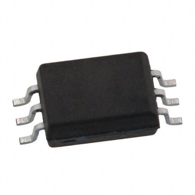
| 产品图片 |
|
| 产品型号 | LT1352IS8 |
| rohs | 含铅 / 不符合限制有害物质指令(RoHS)规范要求 |
| 产品系列 | C-Load™ |
| 产品目录页面 | |
| 供应商器件封装 | 8-SO |
| 包装 | 管件 |
| 压摆率 | 200 V/µs |
| 增益带宽积 | 3MHz |
| 安装类型 | 表面贴装 |
| 封装/外壳 | 8-SOIC(0.154",3.90mm 宽) |
| 工作温度 | -40°C ~ 85°C |
| 放大器类型 | 电压反馈 |
| 标准包装 | 100 |
| 电压-电源,单/双 (±) | ±2.5 V ~ 15 V |
| 电压-输入失调 | 200µV |
| 电流-电源 | 250µA |
| 电流-输入偏置 | 20nA |
| 电流-输出/通道 | 13.4mA |
| 电路数 | 2 |
| 输出类型 | - |



- 商务部:美国ITC正式对集成电路等产品启动337调查
- 曝三星4nm工艺存在良率问题 高通将骁龙8 Gen1或转产台积电
- 太阳诱电将投资9.5亿元在常州建新厂生产MLCC 预计2023年完工
- 英特尔发布欧洲新工厂建设计划 深化IDM 2.0 战略
- 台积电先进制程称霸业界 有大客户加持明年业绩稳了
- 达到5530亿美元!SIA预计今年全球半导体销售额将创下新高
- 英特尔拟将自动驾驶子公司Mobileye上市 估值或超500亿美元
- 三星加码芯片和SET,合并消费电子和移动部门,撤换高东真等 CEO
- 三星电子宣布重大人事变动 还合并消费电子和移动部门
- 海关总署:前11个月进口集成电路产品价值2.52万亿元 增长14.8%

PDF Datasheet 数据手册内容提取
LT1352/LT1353 Dual and Quad m m 250 A, 3MHz, 200V/ s Operational Amplifiers FEATURES DESCRIPTIOU n 3MHz Gain Bandwidth The LT®1352/LT1353 are dual and quad, very low power, n 200V/m s Slew Rate high speed operational amplifiers with outstanding AC n 250m A Supply Current per Amplifier and DC performance. The amplifiers feature much lower n C-LoadTM Op Amp Drives All Capacitive Loads supply current and higher slew rate than devices with n Unity-Gain Stable comparable bandwidth. The circuit combines the slewing n Maximum Input Offset Voltage: 600m V performance of a current feedback amplifier in a true n Maximum Input Bias Current: 50nA operational amplifier with matched high impedance n Maximum Input Offset Current: 15nA inputs. The high slew rate ensures that the large-signal n Minimum DC Gain, R = 2k: 30V/mV bandwidth is not degraded. Each output is capable of L n Input Noise Voltage: 14nV/(cid:214) Hz driving a 1kW load to – 13V with – 15V supplies and a 500W n Settling Time to 0.1%, 10V Step: 700ns load to – 3.4V on – 5V supplies. n Settling Time to 0.01%, 10V Step: 1.25m s The LT1352/LT1353 are members of a family of fast, high n Minimum Output Swing into 1k: – 13V performance amplifiers using this unique topology and n Minimum Output Swing into 500W : – 3.4V employing Linear Technology Corporation’s advanced n Specified at – 2.5V, – 5V and – 15V complementary bipolar processing. For higher bandwidth n Available in SO-8 Package devices with higher supply current see the LT1354 through n LT1353 in Narrow Surface Mount Package LT1365 data sheets. Bandwidths of 12MHz, 25MHz, 50MHz and 70MHz are available with 1mA, 2mA, 4mA and 6mA of APPLICATIOUS supply current per amplifier. Singles, duals and quads of each amplifier are available. The LT1352 is available in an n Battery-Powered Systems 8-lead SO package. The LT1353 is offered in a 14-lead n Wideband Amplifiers narrow surface mount package. n Buffers n Active Filters , LTC and LT are registered trademarks of Linear Technology Corporation. C-Load is a trademark of Linear Technology Corporation. n Data Acquisition Systems n Photodiode Amplifiers TYPICAL APPLICATIOU Instrumentation Amplifier Large-Signal Response R1 R2 R5 R4 50k 5k 1.1k 50k – R3 1/2 5k – LT1352 – + LT11/3252 VOUT VIN + + GAIN = [R4/R3][1 + (1/2)(R2/R1 + R3/R4) + (R2 + R3)/R5] = 102 TRIM R5 FOR GAIN TRIM R1 FOR COMMON MODE REJECTION BW = 30kHz 1352/53 TA01 AV = –1 1352/53 TA02 13523fa 1
LT1352/LT1353 ABSOLUTE WMAXIWMUWM RATINUGS (Note 1) Total Supply Voltage (V+ to V–) .............................. 36V Specified Temperature Range (Note 7).. –40(cid:176) C to 85(cid:176) C Differential Input Voltage (Transient Only, Note 2) – 10V Maximum Junction Temperature (See Below) Input Voltage.......................................................... – V Plastic Package ............................................... 150(cid:176) C S Output Short-Circuit Duration (Note 3)........... Indefinite Storage Temperature Range................. –65(cid:176) C to 150(cid:176) C Operating Temperature Range................ –40(cid:176) C to 85(cid:176) C Lead Temperature (Soldering, 10 sec)..................300(cid:176) C PACKAGE/ORDER IUNFORWMATIOUN TOP VIEW ORDER PART TOP VIEW ORDER PART NUMBER NUMBER OUT A 1 8 V+ OUT A 1 14 OUT D –IN A 2 13 –IN D –IN A 2 7 OUT B LT1352CN8 A D LT1353CS A +IN A 3 12 +IN D +IN A 3 6 –IN B LT1352CS8 V– 4 B 5 +IN B LT1352IN8 V+ 4 11 V– +IN B 5 10 +IN C LT1352IS8 B C N8 PACKAGE –IN B 6 9 –IN C 8-LEAD PDIP S8 PART MARKING OUT B 7 8 OUT C S8 PACKAGE 8-LEAD PLASTIC SO 1352 S PACKAGE TJMAX = 150(cid:176)C, q JA = 130(cid:176)C/W (N8) 14-LEAD PLASTIC SO TJMAX = 150(cid:176)C, q JA = 190(cid:176)C/W (S8) 1352I TJMAX = 150(cid:176)C, q JA = 150(cid:176)C/W Consult LTC Marketing for parts specified with wider operating temperature ranges. ELECTRICAL CHARACTERISTICS T = 25(cid:176) C, V = 0V unless otherwise noted A CM SYMBOL PARAMETER CONDITIONS V MIN TYP MAX UNITS SUPPLY V Input Offset Voltage – 15V 0.2 0.6 mV OS – 5V 0.2 0.6 mV – 2.5V 0.3 0.8 mV I Input Offset Current – 2.5V to – 15V 5 15 nA OS I Input Bias Current – 2.5V to – 15V 20 50 nA B e Input Noise Voltage f = 10kHz – 2.5V to – 15V 14 nV/(cid:214) Hz n i Input Noise Current f = 10kHz – 2.5V to – 15V 0.5 pA/(cid:214) Hz n R Input Resistance V = – 12V – 15V 300 600 MW IN CM Differential – 15V 20 MW C Input Capacitance – 15V 3 pF IN Positive Input Voltage Range – 15V 12.0 13.5 V – 5V 2.5 3.5 V – 2.5V 0.5 1.0 V Negative Input Voltage Range – 15V –13.5 –12.0 V – 5V –3.5 –2.5 V – 2.5V –1.0 –0.5 V CMRR Common Mode Rejection Ratio V = – 12V – 15V 80 94 dB CM V = – 2.5V – 5V 78 86 dB CM V = – 0.5V – 2.5V 68 77 dB CM PSRR Power Supply Rejection Ratio V = – 2.5V to – 15V 90 106 dB S 13523fa 2
LT1352/LT1353 ELECTRICAL CHARACTERISTICS T = 25(cid:176) C, V = 0V unless otherwise noted A CM SYMBOL PARAMETER CONDITIONS V MIN TYP MAX UNITS SUPPLY A Large-Signal Voltage Gain V = – 12V, R = 5k – 15V 40 80 V/mV VOL OUT L V = – 10V, R = 2k – 15V 30 60 V/mV OUT L V = – 10V, R = 1k – 15V 20 40 V/mV OUT L V = – 2.5V, R = 5k – 5V 30 60 V/mV OUT L V = – 2.5V, R = 2k – 5V 25 50 V/mV OUT L V = – 2.5V, R = 1k – 5V 15 30 V/mV OUT L V = – 1V, R = 5k – 2.5V 20 40 V/mV OUT L V Output Swing R = 5k, V = – 10mV – 15V 13.5 14.0 – V OUT L IN R = 2k, V = – 10mV – 15V 13.4 13.8 – V L IN R = 1k, V = – 10mV – 15V 13.0 13.4 – V L IN R = 1k, V = – 10mV – 5V 3.5 4.0 – V L IN R = 500W , V = – 10mV – 5V 3.4 3.8 – V L IN R = 5k, V = – 10mV – 2.5V 1.3 1.7 – V L IN I Output Current V = – 13V – 15V 13.0 13.4 mA OUT OUT V = – 3.4V – 5V 6.8 7.6 mA OUT I Short-Circuit Current V = 0V, V = – 3V – 15V 30 45 mA SC OUT IN SR Slew Rate A = –1, R = 5k (Note 4) – 15V 120 200 V/m s V L – 5V 30 50 V/m s Full-Power Bandwidth 10V Peak (Note 5) – 15V 3.2 MHz 3V Peak (Note 5) – 5V 2.6 MHz GBW Gain Bandwidth f = 200kHz, R = 10k – 15V 2.0 3.0 MHz L – 5V 1.8 2.7 MHz – 2.5V 2.5 MHz t, t Rise Time, Fall Time A = 1, 10% to 90%, 0.1V – 15V 46 ns r f V – 5V 53 ns Overshoot A = 1, 0.1V – 15V 13 % V – 5V 16 % Propagation Delay 50% V to 50% V , 0.1V – 15V 41 ns IN OUT – 5V 52 ns t Settling Time 10V Step, 0.1%, A = –1 – 15V 700 ns s V 10V Step, 0.01%, A = –1 – 15V 1250 ns V 5V Step, 0.1%, A = –1 – 5V 950 ns V 5V Step, 0.01%, A = –1 – 5V 1400 ns V R Output Resistance A = 1, f = 20kHz – 15V 1.5 W O V Channel Separation V = – 10V, R = 2k – 15V 101 120 dB OUT L I Supply Current Each Amplifier – 15V 250 320 m A S Each Amplifier – 5V 230 300 m A 0(cid:176) C £ T £ 70(cid:176) C, V = 0V unless otherwise noted A CM SYMBOL PARAMETER CONDITIONS V MIN TYP MAX UNITS SUPPLY V Input Offset Voltage – 15V 0.8 mV OS – 5V 0.8 mV – 2.5V 1.0 mV Input V Drift (Note 6) – 2.5V to – 15V 3 8 m V/(cid:176) C OS I Input Offset Current – 2.5V to – 15V 20 nA OS I Input Bias Current – 2.5V to – 15V 75 nA B 13523fa 3
LT1352/LT1353 ELECTRICAL CHARACTERISTICS 0(cid:176) C £ T £ 70(cid:176) C, V = 0V unless otherwise noted A CM SYMBOL PARAMETER CONDITIONS V MIN TYP MAX UNITS SUPPLY CMRR Common Mode Rejection Ratio V = – 12V – 15V 78 dB CM V = – 2.5V – 5V 77 dB CM V = – 0.5V – 2.5V 67 dB CM PSRR Power Supply Rejection Ratio V = – 2.5V to – 15V 89 dB S A Large-Signal Voltage Gain V = – 12V, R = 5k – 15V 25 V/mV VOL OUT L V = – 10V, R = 2k – 15V 20 V/mV OUT L V = – 2.5V, R = 5k – 5V 20 V/mV OUT L V = – 2.5V, R = 2k – 5V 15 V/mV OUT L V = – 2.5V, R = 1k – 5V 10 V/mV OUT L V = – 1V, R = 5k – 2.5V 15 V/mV OUT L V Output Swing R = 5k, V = – 10mV – 15V 13.4 – V OUT L IN R = 2k, V = – 10mV – 15V 13.3 – V L IN R = 1k, V = – 10mV – 15V 12.0 – V L IN R = 1k, V = – 10mV – 5V 3.4 – V L IN R = 500W , V = – 10mV – 5V 3.3 – V L IN R = 5k, V = – 10mV – 2.5V 1.2 – V L IN I Output Current V = – 12V – 15V 12.0 mA OUT OUT V = – 3.3V – 5V 6.6 mA OUT I Short-Circuit Current V = 0V, V = – 3V – 15V 24 mA SC OUT IN SR Slew Rate A = –1, R = 5k (Note 4) – 15V 100 V/m s V L – 5V 21 V/m s GBW Gain Bandwidth f = 200kHz, R = 10k – 15V 1.8 MHz L – 5V 1.6 MHz Channel Separation V = – 10V, R = 2k – 15V 100 dB OUT L I Supply Current Each Amplifier – 15V 350 m A S Each Amplifier – 5V 330 m A –40(cid:176) C £ T £ 85(cid:176) C, V = 0V unless otherwise noted (Note 7) A CM SYMBOL PARAMETER CONDITIONS V MIN TYP MAX UNITS SUPPLY V Input Offset Voltage – 15V 1.0 mV OS – 5V 1.0 mV – 2.5V 1.2 mV Input V Drift (Note 6) – 2.5V to – 15V 3 8 m V/(cid:176) C OS I Input Offset Current – 2.5V to – 15V 50 nA OS I Input Bias Current – 2.5V to – 15V 100 nA B CMRR Common Mode Rejection Ratio V = – 12V – 15V 76 dB CM V = – 2.5V – 5V 76 dB CM V = – 0.5V – 2.5V 66 dB CM PSRR Power Supply Rejection Ratio V = – 2.5V to – 15V 87 dB S A Large-Signal Voltage Gain V = – 12V, R = 5k – 15V 20 V/mV VOL OUT L V = – 10V, R = 2k – 15V 15 V/mV OUT L V = – 2.5V, R = 5k – 5V 15 V/mV OUT L V = – 2.5V, R = 2k – 5V 10 V/mV OUT L V = – 2.5V, R = 1k – 5V 8 V/mV OUT L V = – 1V, R = 5k – 2.5V 10 V/mV OUT L 13523fa 4
LT1352/LT1353 ELECTRICAL CHARACTERISTICS –40(cid:176) C £ T £ 85(cid:176) C, V = 0V unless otherwise noted (Note 7) A CM SYMBOL PARAMETER CONDITIONS V MIN TYP MAX UNITS SUPPLY V Output Swing R = 5k, V = – 10mV – 15V 13.3 – V OUT L IN R = 2k, V = – 10mV – 15V 13.2 – V L IN R = 1k, V = – 10mV – 15V 10.0 – V L IN R = 1k, V = – 10mV – 5V 3.3 – V L IN R = 500W , V = – 10mV – 5V 3.2 – V L IN R = 5k, V = – 10mV – 2.5V 1.1 – V L IN I Output Current V = – 10V – 15V 10.0 mA OUT OUT V = – 3.2V – 5V 6.4 mA OUT I Short-Circuit Current V = 0V, V = – 3V – 15V 20 mA SC OUT IN SR Slew Rate A = –1, R = 5k (Note 4) – 15V 50 V/m s V L – 5V 15 V/m s GBW Gain Bandwidth f = 200kHz, R = 10k – 15V 1.6 MHz L – 5V 1.4 MHz Channel Separation V = – 10V, R = 2k – 15V 99 dB OUT L I Supply Current Each Amplifier – 15V 380 m A S Each Amplifier – 5V 350 m A Note 1: Absolute Maximum Ratings are those values beyond which the life input for – 15V supplies and – 2V on the output with – 3V input for – 5V of a device may be impaired. supplies. Note 2: Differential inputs of – 10V are appropriate for transient operation Note 5: Full-power bandwidth is calculated from the slew rate only, such as during slewing. Large, sustained differential inputs will cause measurement: FPBW = (Slew Rate)/2p V . P excessive power dissipation and may damage the part. See Input Note 6: This parameter is not 100% tested. Considerations in the Applications Information section of this data sheet Note 7: The LT1352C/LT1353C are guaranteed to meet specified for more details. performance from 0(cid:176) C to 70(cid:176) C. The LT1352C/LT1353C are designed, Note 3: A heat sink may be required to keep the junction temperature characterized and expected to meet specified performance from below absolute maximum when the output is shorted indefinitely. –40(cid:176) C to 85(cid:176) C but are not tested or QA sampled at these temperatures. Note 4: Slew rate is measured between – 8V on the output with – 12V The LT1352I/LT1353I are guaranteed to meet specified performance from␣–40(cid:176) C to 85(cid:176) C. TYPICAL PERFORWMANUCE CHARACTERISTICS Supply Current vs Supply Voltage Input Common Mode Range Input Bias Current and Temperature vs Supply Voltage vs Input Common Mode Voltage 350 V+ 30 A) –0.5 DTAV O=S 2 =5 °1CmV VTAS == 2– 51°5CV mMPLIFIER ( 300 125°C NGE (V)––11..50 NT (nA) 20 IB = IB+ 2+ IB– CURRENT PER A 220500 –2555°°CC MMON MODE RA–122...500 PUT BIAS CURRE 100 LY 150 CO 1.0 IN–10 P P U 0.5 S 100 V– –20 0 5 10 15 20 0 5 10 15 20 –15 –10 –5 0 5 10 15 SUPPLY VOLTAGE (– V) SUPPLY VOLTAGE (– V) INPUT COMMON MODE VOLTAGE (V) 1352/53 G01 1352/53 G02 1352/53 G03 13523fa 5
LT1352/LT1353 TYPICAL PERFORWMANUCE CHARACTERISTICS Input Bias Current vs Temperature Input Noise Spectral Density Open-Loop Gain vs Resistive Load 40 100 10 110 INPUT BIAS CURRENT (nA) 112233226088264 VISB == –I1B5+V 2+ IB– (cid:214)PUT VOLTAGE NOISE (nV/Hz) 10 einn ARTVASVS ==== 2–115010°150CVk 1 INPUT CURRENT NOISE (pA/H(cid:214) OPEN-LOOP GAIN (dB)190870000 TA = 25°C VS = – 15VVS = – 5V IN z) 4 0 1 0.1 60 –50 –25 0 25 50 75 100 125 1 10 100 1k 10k 10 100 1k 10k TEMPERATURE (°C) FREQUENCY (Hz) LOAD RESISTANCE (W ) 1352/53 G04 1352/53 G05 1352/53 G06 Output Voltage Swing Output Voltage Swing Open-Loop Gain vs Temperature vs Supply Voltage vs Load Current 100 V+ V+ VVSO == ––1125VV –1 RL = 2k –0.5 VVSIN = = – 150VmV 25°C 85°C OPEN-LOOP GAIN (dB) 99999678 RL = 5k TPUT VOLTAGE SWING (V) ––3232 VTAIN = = 2 –51°0CmV RRLL == 11kk TPUT VOLTAGE SWING (V)–––21211.....05005 –40°82C55°°CC –40–°4C0°C –40°C 8255°°CC 95 OU 1 RL = 2k OU 10..05 8255°C°C 94 V– V– –50 –25 0 25 50 75 100 125 0 5 10 15 20 –20 –15 –10 –5 0 5 10 15 20 TEMPERATURE (°C) SUPPLY VOLTAGE (V) OUTPUT CURRENT (mA) 1352/53 G07 1352/53 G08 1352/53 G09 Output Short-Circuit Current Settling Time vs Output Step Settling Time vs Output Step vs Temperature (Noninverting) (Inverting) 60 10 10 NT (mA) 55 VS = – 15V 68 68 E 10mV 1mV UIT CURR 4550 SINK TEP (V) 42 TEP (V) 24 10mV 1mV RC SOURCE T S 0 T S 0 UTPUT SHORT-CI 343005 OUTPU ––––8426 10mV 1mV AOF1VI.SVUL6 TTM==PE H–1RU1z:T5V OUTPU ––––2648 10mV ARVCSVFG ==== 5––Rp11FF5 =V 2k 1mV O LPF RL = 2k 25 –10 –10 –50 –25 0 25 50 75 100 125 0.7 0.8 0.9 1 1.1 1.2 1.3 1.4 1.5 1.6 0.5 0.6 0.7 0.8 0.9 1.0 1.1 1.2 1.3 1.4 1.5 TEMPERATURE (°C) SETTLING TIME (m s) SETTLING TIME (m s) 1352/53 G10 1352/53 G11 1352/53 G12 13523fa 6
LT1352/LT1353 TYPICAL PERFORWMANUCE CHARACTERISTICS Frequency Response Gain and Phase vs Frequency Output Impedance vs Frequency vs Capacitive Load 70 120 1000 10 TA = 25°C TA = 25°C TA = 25°C 60 AV = –1 100 VS = – 15V 8 VS = – 15V PHASE RF = RG = 5k 100 6 AV = –1 GAIN (dB) 24530000 VS = – 5VVGSA =IN – 15VVS = – 5VVS = – 15V 26840000 PHASE (DEG) WUT IMPEDANCE () 110 AV = 100AV = 10 AV = 1 GAIN (dB) –2240 RFB = RG = 5Ck =C 1=0 500pC0F p=F 10pFC =C 5 =0 0100p0F0pF P T –4 10 0 OU 0.1 –6 0 –20 –8 –10 –40 0.01 –10 1k 10k 100k 1M 10M 100M 1k 10k 100k 1M 10M 10k 100k 1M 10M FREQUENCY (Hz) FREQUENCY (Hz) FREQUENCY (Hz) 1352/53 G13 1352/53 G14 1352/53 G15 Gain Bandwidth and Phase Margin Frequency Response Frequency Response vs Temperature vs Supply Voltage (A = 1) vs Supply Voltage (A = –1) V V 4.50 50 5 5 4.25 VS = – 15V 48 4 ATAV == 215°C 4 ATAV == 2–51°C 4.00 VS = – 5V 46 3 RL = 5k 3 RF = RG = 5k GAIN BANDWIDTH (MHz)233323......702755505500 GPAHINAVV SSBS EA == N M ––D1A5W5RVVGIDINTH 334434680442 PHASE MARGIN (DEG) GAIN (dB) –––311220 ––2–1.555VVV GAIN (dB) –––311220 – –155VV 2.25 32 –4 –4 – 2.5V 2.00 30 –5 –5 –50 –25 0 25 50 75 100 125 10k 100k 1M 10M 10k 100k 1M 10M TEMPERATURE (°C) FREQUENCY (Hz) FREQUENCY (Hz) 1352/53 G16 1352/53 G17 1352/53 G18 Gain Bandwidth and Phase Margin Power Supply Rejection Ratio Common Mode Rejection Ratio vs Supply Voltage vs Frequency vs Frequency 4.50 50 120 120 4.25 TA = 25°C 48 dB) VTAS == 2– 51°5CV dB) VTAS == 2– 51°5CV 4.00 46 O (100 O (100 DTH (MHz)33..7550 PHASE MARGIN 4442 PHASE M CTION RATI 80 –PSRR = +PSRR CTION RATI 80 GAIN BANDWI2323....70525005 GAIN BANDWIDTH 33346840 ARGIN (DEG) WER SUPPLY REJE 246000 MMON MODE REJE 246000 2.25 32 O O P C 2.00 30 0 0 0 5 10 15 20 10 100 1k 10k 100k 1M 10M 100 1k 10k 100k 1M 10M SUPPLY VOLTAGE (– V) FREQUENCY (Hz) FREQUENCY (Hz) 1352/53 G19 1352/53 G20 1352/53 G21 13523fa 7
LT1352/LT1353 TYPICAL PERFORWMANUCE CHARACTERISTICS Slew Rate vs Supply Voltage Slew Rate vs Temperature Slew Rate vs Input Level 200 250 200 TA = 25°C AV = –1 TA = 25°C s)150 ARSVRF === R–(S1GR =+ 5+k SR–)/2 s)200 VS = – 15V SRRF == R(SGR =+ R+L S =R 5–k)/2 s) 115705 VARSSVRFB === = ––( RS11RG5V += + 5 SkR–)/2 mV/ mV/150 mV/ 125 E ( E ( E ( AT100 AT AT 100 R R R W W 100 W E E E 75 L L L S S S 50 VS = – 5V 50 50 25 0 0 0 0 5 10 15 –50 –25 0 25 50 75 100 125 0 4 8 12 16 20 24 SUPPLY VOLTAGE (– V) TEMPERATURE (°C) INPUT LEVEL (VP-P) 1352/53 G22 1352/53 G23 1352/53 G24 Total Harmonic Distortion Undistorted Output Swing Undistorted Output Swing vs Frequency vs Frequency (– 15V) vs Frequency (– 5V) 1 30 10 ON (%) VRVTASOL ==== 2–525kV1°5PCV-P )P 25 AV = 1 AV = –1 )P 89 MONIC DISTORTI 0.1 UT VOLTAGE (VP- 2105 UT VOLTAGE (VP- 4657 AV = –1 AV = 1 R0.01 P 10 P A T T 3 L H AV = –1 OU OU TOTA 5 RVSL == –5k15V 21 RVSL == –5k5V AV = 1 THD = 1% THD = 1% 0.001 0 0 10 100 1k 10k 100k 10k 100k 1M 10k 100k 1M FREQUENCY (Hz) FREQUENCY (Hz) FREQUENCY (Hz) 1352/53 G25 1352/53 G26 1352/53 G27 2nd and 3rd Harmonic Distortion vs Frequency Crosstalk vs Frequency Capacitive Load Handling –30 –40 100 AVSV == –115V –50 TAAV == 215°C 90 VTAS == 2– 51°5CV dB)–40 RVOL == 52kVP-P –60 RVILN = = 1 1k5dBm 80 RL = 5k N ( 70 DISTORTIO––5600 3RD HARMONIC STALK (dB)––8700 SHOOT (%) 6500 AV = 1 MONIC –70 CROS–90 OVER 4300 AV = –1 HAR–80 2ND HARMONIC –100 20 –110 10 –90 –120 0 100k 1M 100 1k 10k 100k 1M 10M 10p 100p 1n 10n 0.1m 1m FREQUENCY (Hz) FREQUENCY (Hz) CAPACITIVE LOAD (F) 1352/53 G28 1352/53 G29 1352/53 G30 13523fa 8
LT1352/LT1353 TYPICAL PERFORWMANUCE CHARACTERISTICS Small-Signal Transient Small-Signal Transient Small-Signal Transient (A = 1) (A = –1) (A = –1, C = 1000pF) V V V L 1352/53 G31 1352/53 G32 1352/53 G33 Large-Signal Transient Large-Signal Transient Large-Signal Transient (A = 1) (A = –1) (A = 1, C = 10,000pF) V V V L 1352/53 G34 1352/53 G35 1352/53 G36 APPLICATIOUNS INUFORWMATIOUN Layout and Passive Components Capacitive Loading The LT1352/LT1353 amplifiers are easy to use and toler- The LT1352/LT1353 are stable with any capacitive load. ant of less than ideal layouts. For maximum performance As the capacitive load increases, both the bandwidth and (for example, fast 0.01% settling) use a ground plane, phase margin decrease so there will be peaking in the short lead lengths and RF-quality bypass capacitors (0.01m F frequency domain and in the transient response. Graphs to 0.1m F). For high drive current applications use low ESR of Frequency Response vs Capacitive Load, Capacitive bypass capacitors (1m F to 10m F tantalum). Load Handling and the transient response photos clearly show these effects. The parallel combination of the feedback resistor and gain setting resistor on the inverting input can combine Input Considerations with the input capacitance to form a pole which can cause peaking or even oscillations. If feedback resistors greater Each of the LT1352/LT1353 inputs is the base of an NPN than 10k are used, a parallel capacitor of value, C > and a PNP transistor whose base currents are of opposite F (R )(C /R ), should be used to cancel the input pole and polarity and provide first-order bias current cancellation. G IN F optimize dynamic performance. For applications where Because of variation in the matching of NPN and PNP beta, the DC noise gain is one and a large feedback resistor is the polarity of the input bias current can be positive or used, C should be greater than or equal to C . An negative. The offset current does not depend on NPN/PNP F IN example would be an I-to-V converter as shown in the beta matching and is well controlled. The use of balanced Typical Applications section. source resistance at each input is recommended for 13523fa 9
LT1352/LT1353 APPLICATIOUNS INUFORWMATIOUN applications where DC accuracy must be maximized. The input step. The graph Slew Rate vs Input Level illustrates inputs can withstand transient differential input voltages this relationship. In higher gain configurations the large- up to 10V without damage and need no clamping or source signal performance and the small-signal performance resistance for protection. Differential inputs, however, both look like a single pole response. generate large supply currents (tens of mA) as required for Capacitive load compensation is provided by the RC, CC high slew rates. If the device is used with sustained network which is bootstrapped across the output stage. differential inputs, the average supply current will in- When the amplifier is driving a light load the network has crease, excessive power dissipation will result and the part no effect. When driving a capacitive load (or a low value may be damaged. The part should not be used as a resistive load) the network is incompletely bootstrapped comparator, peak detector or other open-loop applica- and adds to the compensation at the high impedance tion with large, sustained differential inputs. Under node. The added capacitance slows down the amplifier normal, closed-loop operation, an increase of power dis- and a zero is created by the RC combination, both of which sipation is only noticeable in applications with large slewing improve the phase margin. The design ensures that even outputs and is proportional to the magnitude of the for very large load capacitances, the total phase lag can differential input voltage and the percent of time that the never exceed 180 degrees (zero phase margin) and the inputs are apart. Measure the average supply current for amplifier remains stable. the application in order to calculate the power dissipation. Power Dissipation Circuit Operation The LT1352/LT1353 combine high speed and large output The LT1352/LT1353 circuit topology is a true voltage drive in small packages. Because of the wide supply feedback amplifier that has the slewing behavior of a voltage range, it is possible to exceed the maximum current feedback amplifier. The operation of the circuit can junction temperature of 150(cid:176) C under certain conditions. be understood by referring to the Simplified Schematic. Maximum junction temperature T is calculated from the J The inputs are buffered by complementary NPN and PNP ambient temperature T and power dissipation P as A D emitter followers which drive R1, a 1k resistor. The input follows: voltage appears across the resistor generating currents LT1352CN8: T = T + (P )(130(cid:176) C/W) J A D which are mirrored into the high impedance node and LT1352CS8: T = T + (P )(190(cid:176) C/W) J A D compensation capacitor C . Complementary followers T LT1353CS: T = T + (P )(150(cid:176) C/W) J A D form an output stage which buffers the gain node from the load. The output devices Q19 and Q22 are connected to Worst-case power dissipation occurs at the maximum form a composite PNP and a composite NPN. supply current and when the output voltage is at 1/2 of either supply voltage (or the maximum swing if less than The bandwidth is set by the input resistor and the capaci- 1/2 supply voltage). For each amplifier P is: D(MAX) tance on the high impedance node. The slew rate is determined by the current available to charge the high PD(MAX) =(V+ – V–)(IS(MAX)) + (V+/2)2/RL or impedance node capacitance. This current is the differen- (V+ – V–)(IS(MAX)) + (V+ – VMAX)(IMAX) tial input voltage divided by R1, so the slew rate is Example: LT1353 in S14 at 85(cid:176) C, V = – 15V, R = 500W , S L proportional to the input. Highest slew rates are therefore V = – 5V (– 10mA) OUT seen in the lowest gain configurations. For example, a 10V P = (30V)(380m A) + (15V – 5V)(10mA) = 111mW output step in a gain of 10 has only a 1V input step whereas D(MAX) T = 85(cid:176) C + (4)(111mW)(150(cid:176) C/W) = 152(cid:176) C the same output step in unity gain has a 10 times greater J 13523fa 10
LT1352/LT1353 SI W PLIFIED SCHEW ATIC V+ R2 R3 Q11 Q10 Q12 Q20 Q21 C1 R6 Q9 Q19 Q7 R1 Q3 Q17 CC Q5 1k Q1 RC –IN Q6 Q2 +IN OUTPUT Q18 Q8 Q4 R7 Q13 Q22 C2 CT Q15 Q14 Q16 Q23 Q24 R4 R5 V– 1352/53 SS 13523fa 11
LT1352/LT1353 TYPICAL APPLICATIONUS DAC I-to-V Converter 10pF 12 5k DAC – INPUTS 1/2 565A TYPE LT1352 VOUT + VOS + IOS (5kW ) + VA OV OU LT < 0.5LSB 5k 1352/53 TA03 400kHz Photodiode Preamp with 10kHz Highpass Loop 1N5712 10k – 1/2 BPV22NF LT1352 VOUT 1.5k + 10k + 1/2 10nF LT1352 – 10nF 10k 1352/53 TA05 13523fa 12
LT1352/LT1353 PACKAGE DESCRIPTIOUN N8 Package 8-Lead PDIP (Narrow .300 Inch) (Reference LTC DWG # 05-08-1510) .400* (10.160) MAX 8 7 6 5 .255 – .015* (6.477 – 0.381) 1 2 3 4 .300 – .325 .045 – .065 .130 – .005 (7.620 – 8.255) (1.143 – 1.651) (3.302 – 0.127) .065 (1.651) .008 – .015 TYP (0.203 – 0.381) .120 (3.048) .020 +.035 MIN (0.508) .325 ( –.015 ) .100 .018 – .003 MIN 8.255+0.889 (2.54) (0.457 – 0.076) –0.381 BSC N8 1002 NOTE: INCHES 1. DIMENSIONS ARE MILLIMETERS *THESE DIMENSIONS DO NOT INCLUDE MOLD FLASH OR PROTRUSIONS. MOLD FLASH OR PROTRUSIONS SHALL NOT EXCEED .010 INCH (0.254mm) 13523fa 13
LT1352/LT1353 PACKAGE DESCRIPTIOUN S8 Package 8-Lead Plastic Small Outline (Narrow .150 Inch) (Reference LTC DWG # 05-08-1610) .189 – .197 .045 – .005 (4.801 – 5.004) .050 BSC NOTE 3 8 7 6 5 .245 MIN .160 – .005 .150 – .157 .228 – .244 (3.810 – 3.988) (5.791 – 6.197) NOTE 3 .030 – .005 TYP 1 2 3 4 RECOMMENDED SOLDER PAD LAYOUT .010 – .020 · 45(cid:176) .053 – .069 (0.254 – 0.508) (1.346 – 1.752) .004 – .010 .008 – .010 (0.203 – 0.254) 0°– 8° TYP (0.101 – 0.254) .016 – .050 .014 – .019 .050 (0.406 – 1.270) (0.355 – 0.483) (1.270) NOTE: INCHES TYP BSC 1. DIMENSIONS IN (MILLIMETERS) 2. DRAWING NOT TO SCALE 3. THESE DIMENSIONS DO NOT INCLUDE MOLD FLASH OR PROTRUSIONS. MOLD FLASH OR PROTRUSIONS SHALL NOT EXCEED .006" (0.15mm) SO8 0303 13523fa 14
LT1352/LT1353 PACKAGE DESCRIPTIOUN S Package 14-Lead Plastic Small Outline (Narrow .150 Inch) (Reference LTC DWG # 05-08-1610) .337 – .344 .045 – .005 (8.560 – 8.738) .050 BSC NOTE 3 14 13 12 11 10 9 8 N N .245 MIN .160 – .005 .228 – .244 .150 – .157 (5.791 – 6.197) (3.810 – 3.988) NOTE 3 1 2 3 N/2 N/2 .030 – .005 TYP RECOMMENDED SOLDER PAD LAYOUT 1 2 3 4 5 6 7 .010 – .020 · 45° .053 – .069 (0.254 – 0.508) (1.346 – 1.752) .008 – .010 .004 – .010 (0.203 – 0.254) 0° – 8° TYP (0.101 – 0.254) .016 – .050 .014 – .019 .050 (0.406 – 1.270) (0.355 – 0.483) (1.270) TYP BSC NOTE: INCHES S14 0502 1. DIMENSIONS IN (MILLIMETERS) 2. DRAWING NOT TO SCALE 3. THESE DIMENSIONS DO NOT INCLUDE MOLD FLASH OR PROTRUSIONS. MOLD FLASH OR PROTRUSIONS SHALL NOT EXCEED .006" (0.15mm) 13523fa Information furnished by Linear Technology Corporation is believed to be accurate and reliable. 15 However, no responsibility is assumed for its use. Linear Technology Corporation makes no represen- tation that the interconnection of its circuits as described herein will not infringe on existing patent rights.
LT1352/LT1353 TYPICAL APPLICATIONUS 20kHz, 4th Order Butterworth Filter 4.64k 5.49k 470pF 220pF 4.64k 13.3k VIN – 1/2 5.49k 11.3k – 2200pF LT1352 + 4700pF LT11/3252 VOUT + 1352/53 TA04 RELATED PARTS PART NUMBER DESCRIPTION COMMENTS LT1351 250m A, 3MHz, 200V/m s Op Amp Good DC Precision, C-Load Stable, Power Saving Shutdown LT1354/55/56 Single/Dual/Quad 1mA, 12MHz, 400V/m s Op Amp Good DC Precision, Stable with All Capacitive Loads 13523fa 16 Linear Technology Corporation LT/TP 0603 1K REV A • PRINTED IN USA 1630 McCarthy Blvd., Milpitas, CA 95035-7417 (408) 432-1900 l FAX: (408) 434-0507 l www.linear.com ª LINEAR TECHNOLOGY CORPORATION 1996
Mouser Electronics Authorized Distributor Click to View Pricing, Inventory, Delivery & Lifecycle Information: A nalog Devices Inc.: LT1352IS8#PBF LT1353CS#TRPBF LT1353CS LT1353CS#PBF LT1352CS8#PBF LT1352IN8 LT1352IN8#PBF LT1352IS8 LT1353CS#TR LT1352CS8#TR LT1352IS8#TRPBF LT1352CN8 LT1352IS8#TR LT1352CS8#TRPBF LT1352CS8 LT1352CN8#PBF

 Datasheet下载