ICGOO在线商城 > 集成电路(IC) > PMIC - 稳压器 - DC DC 开关稳压器 > LT1304CS8-5
 Datasheet下载
- 型号: LT1304CS8-5
- 制造商: LINEAR TECHNOLOGY
- 库位|库存: xxxx|xxxx
- 要求:
| 数量阶梯 | 香港交货 | 国内含税 |
| +xxxx | $xxxx | ¥xxxx |
查看当月历史价格
查看今年历史价格
LT1304CS8-5产品简介:
ICGOO电子元器件商城为您提供LT1304CS8-5由LINEAR TECHNOLOGY设计生产,在icgoo商城现货销售,并且可以通过原厂、代理商等渠道进行代购。 LT1304CS8-5价格参考¥60.64-¥70.42。LINEAR TECHNOLOGYLT1304CS8-5封装/规格:PMIC - 稳压器 - DC DC 开关稳压器, 固定 升压,SEPIC 开关稳压器 IC 正 5V 1 输出 800mA(开关) 8-SOIC(0.154",3.90mm 宽)。您可以下载LT1304CS8-5参考资料、Datasheet数据手册功能说明书,资料中有LT1304CS8-5 详细功能的应用电路图电压和使用方法及教程。
| 参数 | 数值 |
| 产品目录 | 集成电路 (IC) |
| 描述 | IC REG BOOST 5V 0.2A 8SOIC |
| 产品分类 | |
| 品牌 | Linear Technology |
| 数据手册 | http://www.linear.com/docs/1963 |
| 产品图片 |
|
| 产品型号 | LT1304CS8-5 |
| PWM类型 | Burst Mode® |
| rohs | 含铅 / 不符合限制有害物质指令(RoHS)规范要求 |
| 产品系列 | - |
| 产品目录页面 | |
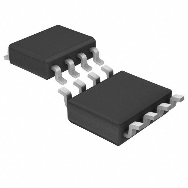
| 供应商器件封装 | 8-SOIC |
| 包装 | 管件 |
| 同步整流器 | 无 |
| 安装类型 | 表面贴装 |
| 封装/外壳 | 8-SOIC(0.154",3.90mm 宽) |
| 工作温度 | 0°C ~ 70°C |
| 标准包装 | 100 |
| 电压-输入 | 1.5 V ~ 8 V |
| 电压-输出 | 5V |
| 电流-输出 | 200mA |
| 类型 | 升压(升压) |
| 输出数 | 1 |
| 输出类型 | 固定 |
| 配用 | /product-detail/zh/DC088A/DC088A-ND/4866526 |
| 频率-开关 | 最高 300kHz |


- 商务部:美国ITC正式对集成电路等产品启动337调查
- 曝三星4nm工艺存在良率问题 高通将骁龙8 Gen1或转产台积电
- 太阳诱电将投资9.5亿元在常州建新厂生产MLCC 预计2023年完工
- 英特尔发布欧洲新工厂建设计划 深化IDM 2.0 战略
- 台积电先进制程称霸业界 有大客户加持明年业绩稳了
- 达到5530亿美元!SIA预计今年全球半导体销售额将创下新高
- 英特尔拟将自动驾驶子公司Mobileye上市 估值或超500亿美元
- 三星加码芯片和SET,合并消费电子和移动部门,撤换高东真等 CEO
- 三星电子宣布重大人事变动 还合并消费电子和移动部门
- 海关总署:前11个月进口集成电路产品价值2.52万亿元 增长14.8%


PDF Datasheet 数据手册内容提取
LT1304/LT1304-3.3/LT1304-5 Micropower DC/DC Converters with Low-Battery Detector Active in Shutdown FEATURES DESCRIPTIOUN n 5V at 200mA from Two Cells The LT®1304 is a micropower step-up DC/DC converter n 10m A Quiescent Current in Shutdown ideal for use in small, low voltage, battery-operated sys- n Operates with V as Low as 1.5V tems. The devices operate from a wide input supply range IN n Low-Battery Detector Active in Shutdown of 1.5V to 8V. The LT1304-3.3 and LT1304-5 generate n Low Switch V : 370mV at 1A Typical regulated outputs of 3.3V and 5V and the adjustable CESAT n 120m A Quiescent Current in Active Mode LT1304 can deliver output voltages up to 25V. Quiescent n Switching Frequency Up to 300kHz current, 120m A in active mode, decreases to just 10m A in n Programmable Peak Current with One Resistor shutdown with the low-battery detector still active. Peak n 8-Lead SO Package switch current, internally set at 1A, can be reduced by adding a single resistor from the I pin to ground. The APPLICATIOUNS LIM high speed operation of the LT1304 allows the use of small, surface-mountable inductors and capacitors. The n 2-, 3-, or 4-Cell to 5V or 3.3V Step-Up LT1304 is available in an 8-lead SO package. n Portable Instruments n Bar Code Scanners , LTC and LT are registered trademarks of Linear Technology Corporation. n Palmtop Computers n Diagnostic Medical Instrumentation n Personal Data Communicators/Computers TYPICAL APPLICATIONU 2-Cell to 5V Step-Up Converter with Low-Battery Detect Efficiency 22m H* D1** 90 3 4 499k VIN SW 80 1 8 5V(cid:13) LBI SENSE 2 CELLS + 100m F 604k 6 LT1304-5 2 100k + 120000mmFA CY (%) 70 (cid:13) NC ILIM LBO LBO(cid:13) EN SHDN GND LVOBAWT <W 2H.E2NV (cid:13) FFICI 60 7 5 E SHUTDOWN 50 VIN = 3.3V(cid:13) VIN = 2.5V(cid:13) *(cid:13)SUMIDA CD54-220(cid:13) VIN = 1.8V **1N5817 1304 TA01 40 0.1 1 10 100 500 LOAD CURRENT (mA) 1304 TA02 1
LT1304/LT1304-3.3/LT1304-5 ABSOLUTE WMAXIWMUWM RATINUGS PACKAGE/ORDER IUNFORWMATIOUN V Voltage ................................................................ 8V IN ORDER PART SW Voltage............................................... –0.4V to 25V NUMBER FB Voltage (LT1304)...................................... VIN + 0.3V TOP VIEW LT1304CS8 Sense Voltage (LT1304-3.3/LT1304-5) ..................... 8V LBI(cid:13) 1(cid:13) 8(cid:13) FB (SENSE)*(cid:13) LT1304CS8-3.3 I Voltage .............................................................. 5V LIM LBO(cid:13) 2(cid:13) 7(cid:13) SHDN(cid:13) LT1304CS8-5 SHDN Voltage............................................................ 6V VIN(cid:13) 3(cid:13) 6(cid:13) ILIM(cid:13) LBI Voltage............................................................... V IN SW 4 5(cid:13) GND LBO Voltage............................................................... 8V (cid:13) S8 PART MARKING S8 PACKAGE(cid:13) Maximum Power Dissipation.............................500mW 8-LEAD PLASTIC SO(cid:13) Junction Temperature.......................................... 125(cid:176) C *FIXED OUTPUT VERSION 1304 Operating Temperature Range.....................0(cid:176) C to 70(cid:176) C TJMAX = 125(cid:176)C, q JA = 150(cid:176)C/W 13043 Storage Temperature Range................. –65(cid:176) C to 150(cid:176) C 13045 Lead Temperature (Soldering, 10 sec)..................300(cid:176) C Consult factory for Industrial and Military grade parts. ELECTRICAL CHARACTERISTICS V = 2V, V = 2V unless otherwise noted. IN SHDN PARAMETER CONDITIONS MIN TYP MAX UNITS Minimum Operating Voltage l 1.5 1.65 V Operating Voltage Range l 8 V Quiescent Current V = 2V, Not Switching l 120 200 m A SHDN Quiescent Current in Shutdown V = 0V, V = 2V l 7 15 m A SHDN IN V = 0V, V = 5V l 27 50 m A SHDN IN Comparator Trip Point LT1304 l 1.22 1.24 1.26 V FB Pin Bias Current LT1304 l 10 25 nA Sense Pin Leakage in Shutdown V = 0V, Fixed Output Versions l 0.002 1 m A SHDN Output Sense Voltage LT1304-3.3 l 3.17 3.3 3.43 V LT1304-5 l 4.80 5.05 5.25 V Line Regulation 1.8V £ V £ 8V l 0.04 0.15 %/V IN LBI Input Threshold Falling Edge l 1.10 1.17 1.25 V LBI Bias Current l 6 20 nA LBI Input Hysteresis l 35 65 mV LBO Output Voltage Low I = 500m A l 0.2 0.4 V SINK LBO Output Leakage Current LBI = 1.5V, LBO = 5V l 0.01 0.1 m A SHDN Input Voltage High l 1.4 V SHDN Input Voltage Low l 0.4 V SHDN Pin Bias Current V = 5V l 5 8 m A SHDN V = 0V l –5 –2 m A SHDN Switch OFF Time l 1 1.5 2 m s Switch ON Time Current Limit Not Asserted l 4 6 8 m s Maximum Duty Cycle Current Limit Not Asserted l 76 80 88 % Peak Switch Current I Pin Open, V = 5V 0.8 1 1.2 A LIM IN 20k from I to GND 500 mA LIM 2
LT1304/LT1304-3.3/LT1304-5 ELECTRICAL CHARACTERISTICS V = 2V, V = 2V unless otherwise noted. IN SHDN PARAMETER CONDITIONS MIN TYP MAX UNITS Switch Saturation Voltage I = 1A 0.37 V SW I = 700mA l 0.26 0.35 V SW Switch Leakage Switch Off, V = 5V l 0.01 7 m A SW The l denotes specifications which apply over the 0(cid:176) C to 70(cid:176) C operating temperature range. TYPICAL PERFORWMAUNCE CHARACTERISTICS Switch Saturation Voltage Peak Switch Current Limit On- and Off-Times 500(cid:13) 1.3(cid:13) 8(cid:13) TA = 25°C 1.2(cid:13) 7(cid:13) MAXIMUM ON-TIME V)400(cid:13) m 6(cid:13) E ( A) 1.1(cid:13) URATION VOLTAG320000(cid:13)(cid:13) PEAK CURRENT ( 100...098(cid:13)(cid:13)(cid:13) mTIME (s) 543(cid:13)(cid:13)(cid:13) AT 2(cid:13) OFF-TIME S100(cid:13) 0.7(cid:13) 1(cid:13) 0 0.6(cid:13) 0 0 0.2 0.4 0.6 0.8 1.0 1.2 –50 –25 0 25 50 75 100 –50 –25 0 25 50 75 100 SWITCH CURRENT (A) (cid:13) TEMPERATURE (°C) TEMPERATURE (°C) 1304 G01 1304 G02 1304 G03 Feedback Voltage Feedback Pin Bias Current Supply Current 1.250(cid:13) 20 300(cid:13) 1.245(cid:13) 18 TA = 25°C 250(cid:13) 1.240(cid:13) 16 FEEDBACK VOLTAGE (V)11111.....222223322150505(cid:13)(cid:13)(cid:13)(cid:13)(cid:13) BIAS CURRENT (nA) 11182460 mSUPPLY CURRENT (A)211050000(cid:13)(cid:13)(cid:13) NOT VSSWHIDTNC H= IVNIGN(cid:13) 1.210(cid:13) 4 50(cid:13) 1.205(cid:13) 2 VSHDN = 0V 1.200 0 0 –50 –25 0 25 50 75 100 –50 –25 0 25 50 75 100 0 1 2 3 4 5 6 7 8 TEMPERATURE (°C) TEMPERATURE (°C) INPUT VOLTAGE (V) 1304 G04 1304 G05 1304 G06 3
LT1304/LT1304-3.3/LT1304-5 TYPICAL PERFORWMAUNCE CHARACTERISTICS Load Transient Response Burst ModeTM Operation VOUT 100mV/DIV VOUT AC COUPLED 100mV/DIV AC COUPLED VSW 5V/DIV ILOAD 200mA0 500mA/DIIVL 100m s/DIV 1304 G07 VIN = 2.5V 20m s/DIV 1304 G08 VOUT = 5V ILOAD = 185mA L = 22m H Burst Mode is a trademark of Linear Technology Corporation. PIUN FUUNCTIOUNS LBI (Pin 1): Low-Battery Detector Input. When voltage on I (Pin 6): Current Limit Set Pin. Float for 1A peak switch LIM this pin is less than 1.17V, detector output is low. current; a resistor to ground will lower peak current. LBO (Pin 2): Low-Battery Detector Output. Open collector SHDN (Pin 7): Shutdown Input. When low, switching can sink up to 500m A. Low-battery detector remains active regulator is turned off. The low-battery detector remains when device is shut down. active. The SHDN input should not be left floating. If SHDN is not used, tie the pin to V . V (Pin 3): Input Supply. Must be bypassed close (<0.2") IN IN to the pin. See required layout in the Typical Applications. FB/SENSE (Pin 8): On the LT1304 (adjustable) this pin goes to the comparator input. On the fixed-output ver- SW (Pin 4): Collector of Power NPN. Keep copper traces on sions, the pin connects to the resistor divider which sets this pin short and direct to minimize RFI. output voltage. The divider is disconnected from the pin GND (Pin 5): Device Ground. Must be low impedance; during shutdown. solder directly to ground plane. 4
LT1304/LT1304-3.3/LT1304-5 BLOCK DIAGRAWS VIN + L1 + VOUT C1 D1 C2 LB0 VIN SW 2 3 4 1.5V(cid:13) UNDERVOLTAGE(cid:13) LOCKOUT LBI 36mV 1 + + A2 R2(cid:13) R1(cid:13) 1k 7.2W – – A3 1.17V BIAS(cid:13) Q3 OFF ~1V R3 FB 8 – 1k ENABLE TIMERS(cid:13) R4 A1 1.65µµss OONF(cid:13)F Q2(cid:13) Q· 210(cid:13) 0 + DRIVER · 1 1.24V(cid:13) VREF SHUTDOWN SHDN ILIM GND 7 6 5 1304 F01 Figure 1. LT1304 Block Diagram. Independent Low-Battery Detector A3 Remains Alive When Device Is in Shutdown LBI LB0 VIN SW 1 2 3 4 1.5V(cid:13) UNDERVOLTAGE(cid:13) LOCKOUT 36mV SENSE 8 + + A2 R2(cid:13) R1(cid:13) 1k 7.2W – – A3 1.17V BIAS(cid:13) Q3 OFF ~1V 590k – 1k ENABLE TIMERS(cid:13) R1 A1 1.65µµss OONF(cid:13)F Q2(cid:13) Q· 210(cid:13) 0 + DRIVER · 1 1.24V(cid:13) VREF SHUTDOWN SHDN ILIM GND 7 6 5 1304 F02 R1 = 355k (LT1304-3.3), 195k (LT1304-5) Figure 2. LT1304-3.3/LT1304-5 Block Diagram 5
LT1304/LT1304-3.3/LT1304-5 OPERATIOU The LT1304’s operation can best be understood by exam- tion in efficiency. For the majority of 2-cell or 3-cell input ining the block diagram in Figure 1. Comparator A1 LT1304 applications, a 22m H or 20m H inductor such as the monitors the output voltage via resistor divider string Sumida CD54-220 (drum) or Coiltronics CTX20-1 (toroid) R3/R4 at the FB pin. When V is higher than the 1.24V will suffice. If switch current is reduced using the I pin, FB LIM reference, A2 and the timers are turned off. Only the smaller inductors such as the Sumida CD43 series or reference, A1 and A3 consume current, typically 120m A. Coilcraft DO1608 series can be used. Minimizing DCR is As V drops below 1.24V plus A1’s hysteresis (about important for best efficiency. Ideally, the inductor DCR FB 6mV), A1 enables the rest of the circuit. Power switch Q1 should be less than 0.05W , although the physical size of is then cycled on for 6m s, or until current comparator A2 such an inductor makes its use prohibitive in many space turns off the ON timer, whichever comes first. Off-time is conscious applications. If EMI is a concern, such as when fixed at approximately 1.5m s. Q1’s switching causes cur- sensitive analog circuitry is present, a toroidal inductor rent to alternately build up in inductor L1 and discharge such as the Coiltronics CTX20-1 is suggested. into output capacitor C2 via D1, increasing the output A special case exists where the V /V differential is OUT IN voltage. As V increases enough to overcome C1’s hys- FB high, such as a 2V to 12V boost converter. If the required teresis, switching action ceases. C2 is left to supply duty cycle for continuous mode operation is higher than current to the load until V decreases enough to force OUT the LT1304 can provide, the converter must be designed A1’s output high, and the entire cycle repeats. for discontinuous operation. This means that the inductor If switch current reaches 1A, causing A2 to trip, switch current decreases to zero during the switch OFF time. For ON time is reduced. This allows continuous mode opera- a simple step-up (boost) converter, duty cycle can be tion during bursts. A2 monitors the voltage across 7.2W calculated by the following formula: resistor R1, which is directly related to the switch current. DC = 1 –[(V – V )/(V + V )] IN SAT OUT D Q2’s collector current is set by the emitter-area ratio to 0.5% of Q1’s collector current. R1’s voltage drop exceeds where, 36mV, corresponding to 1A switch current, A2’s output V = Minimum input voltage IN goes high, truncating the ON time part of the switch cycle. V = Switch saturation voltage (0.3V) SAT The 1A peak current can be reduced by tying a resistor V = Output voltage OUT between the I pin and ground, causing a voltage drop LIM V = Diode forward voltage (0.4V) D to appear across R2. The drop offsets some of the 36mV If the calculated duty cycle exceeds the minimum LT1304 reference voltage, lowering peak current. A 22k resistor duty cycle of 76%, the converter should be designed for limits current to approximately 550mA. A capacitor con- discontinuous mode operation. The inductance must be nected between I and ground provides soft start. Shut- LIM low enough so that current in the inductor reaches the down is accomplished by grounding the SHDN pin. peak current in a single cycle. Inductor value can be The low-battery detector A3 has its own 1.17V reference calculated by: and is always on. The open collector output device can sink up to 500m A. Approximately 35mV of hysteresis is built L = (VIN – VSAT)(tON/1A) into A3 to reduce “buzzing” as the battery voltage reaches where, the trip level. t = Minimum on-time of LT1304 (4m s) ON Inductor Selection One advantage of discontinuous mode operation is that inductor values are usually quite low so very small units Inductors used with the LT1304 must be capable of can be used. Ripple current is higher than with continuous handling the worst-case peak switch current of 1.2A mode designs and efficiency will be somewhat less. without saturating. Open flux rod or drum core units may be biased into saturation by 20% with only a small reduc- 6
LT1304/LT1304-3.3/LT1304-5 OPERATIOU Table 1 lists inductor suppliers along with appropriate part I Function LIM numbers. The LT1304’s current limit (I ) pin can be used for soft LIM Table 1. Recommended Inductors start. Upon start-up, the LT1304 will draw maximum VENDOR SERIES PHONE NUMBER current (about 1A) from the supply to charge the output Sumida CD54, CD43 (708) 956-0666 capacitor. Figure 3 shows VOUT and VIN waveforms as the Coiltronics CTX20-1 (407) 241-7876 device is turned on. The high current flow can create IR Dale LPT4545 (605) 665-9301 drops along supply and ground lines or cause the input supply to drop out momentarily. By adding R1 and C1 as Coilcraft DO3316, DO1608, DO3308 (708) 639-6400 shown in Figure 4, the switch current is initially limited to well under 1A as detailed in Figure 5. Current flowing into Capacitor Selection C1 from R1 and the I pin will eventually charge C1 and LIM Low ESR (Equivalent Series Resistance) capacitors should R1 effectively takes C1 out of the circuit. R1 also provides be used at the output of the LT1304 to minimize output a discharge path for C1 when SHUTDOWN is brought low ripple voltage. High quality input bypassing is also re- for turn-off. quired. For surface mount applications AVX TPS series tantalum capacitors are recommended. These have been specifically designed for switch mode power supplies and VOUT 2V/DIV have low ESR along with high surge current ratings. A 100m F, 10V AVX TPS surface mount capacitor typically IIN limits output ripple voltage to 70mV when stepping up 500mA/DIV from 2V to 5V at a 200mA load. For through hole applica- VSHDN 10V/DIV tions Sanyo OS-CON capacitors offer extremely low ESR 1ms/DIV 1304 F03 in a small package size. Again, if peak switch current is Figure 3. Start-Up Response. Input Current Rises Quickly to reduced using the I pin, capacitor requirements can be LIM 1A. V Reaches 5V in Approximately 1ms. Output Drives OUT eased and smaller, higher ESR units can be used. Sug- 20mA Load gested capacitor sources are listed in Table 2. Table 2. Recommended Capacitors 22m H* MBRS130L VENDOR SERIES TYPE PHONE NUMBER AVX TPS Surface Mount (803) 448-9411 VIN SW Sanyo OS-CON Through Hole (619) 661-6835 LBI SENSE 5V(cid:13) + 200mA Sprague 595D Surface Mount (603) 225-1961 100m F LT1304-5 2 CELLS LB0 SHDN + Diode Selection GND ILIM R1(cid:13) 100m F 1M Best performance is obtained with a Schottky rectifier + C1(cid:13) such as the 1N5818. Motorola makes the MBRS130L 1m F SHUTDOWN Schottky which is slightly better than the 1N5818 and comes in a surface mount package. For lower switch *SUMIDA CD54-220 1304 F04 currents, the MBR0530 is recommended. It comes in a Figure 4. 2-Cell to 5V/200mA Boost Converter Takes Four very small SOD-123 package. Multiple 1N4148s in parallel External Parts. Components with Dashed Lines Are for can be used in a pinch, although efficiency will suffer. Soft Start (Optional) 7
LT1304/LT1304-3.3/LT1304-5 OPERATIOU If the full power capability of the LT1304 is not required, bypass capacitor is required. If the input supply is close to peak switch current can be limited by connecting a resistor the IC, a 1m F ceramic capacitor can be used instead. The R from the I pin to ground. With R = 22k, peak LT1304 switches current in 1A pulses, so a low impedance LIM LIM LIM switch current is reduced to approximately 500mA. Smaller supply must be available. If the power source (for example, power components can then be used. The graph in Figure a 2 AA cell battery) is within 1 or 2 inches of the IC, the 6 shows switch current vs R resistor value. battery itself provides bulk capacitance and the 1m F ce- LIM ramic capacitor acts to smooth voltage spikes at switch turn-on and turn-off. If the power source is far away from VOUT the IC, inductance in the power source leads results in high 2V/DIV impedance at high frequency. A local high capacitance bypass is then required to restore low impedance at the IC. IIN 500mA/DIV VSHDN SHUTDOWN 10V/DIV 1ms/DIV 1304 F05 Figure 5. Start-Up Response with 1m F/1MW Components in Figure 2 Added. Input Current Is More Controlled. V OUT Reaches 5V in 6ms. Output Drives 20mA Load 1 8 2 LT1304 7 1000(cid:13) VIN 3 6 900(cid:13) 4 5 A) m 800(cid:13) T ( CIN N + RE 700(cid:13) VOUT R CU COUT K + A 600(cid:13) E P 500(cid:13) GND (BATTERY AND LOAD RETURN) 400 1304 F07 10 100 1000 RLIM (kW ) Figure 7. Suggested Layout for Best Performance. Input 1304 F06 Capacitor Placement as Shown Is Highly Recommended. (cid:13) Switch Trace (Pin 4) Copper Area Is Minimized Figure 6. Peak Switch Current vs R Value LIM Layout/Input Bypassing Low-Battery Detector The LT1304’s high speed switching mandates careful The LT1304 contains an independent low-battery detector attention to PC board layout. Suggested component place- that remains active when the device is shut down. This ment is shown in Figure 7. The input supply must have low detector, actually a hysteretic comparator, has an open impedance at AC and the input capacitor should be placed collector output that can sink up to 500m A. The compara- as indicated in the figure. The value of this capacitor tor also operates below the switcher’s undervoltage lock- depends on how close the input supply is to the IC. In out threshold, operating until V reaches approximately IN situations where the input supply is more than a few 1.4V. Figure 8 illustrates the input/output characteristic of inches away from the IC, a 47m F to 100m F solid tantalum the detector. Hysteresis is clearly evident in the figure. 8
LT1304/LT1304-3.3/LT1304-5 OPERATIOU 1000(cid:13) VLBO 100(cid:13) 2V/DIV H) S ( R U O H 10(cid:13) VLBI 200mV/DIV 1304 F08 Figure 8. Low-Battery Detector Transfer Function. 1 Pull-Up R = 22k, V = 2V, Sweep Frequency = 10Hz 1 10 100 200 IN LOAD CURRENT (mA) 1304 F10 Battery Life Figure 10. Battery Life vs Load Current. Dots Specify Actual Measurements How may hours does it work? This is the bottom line question that must be asked of any efficiency study. AA 6(cid:13) alkaline cells are not perfect power sources. For efficient power transfer, energy must be taken from AA cells at a 5(cid:13) rate that does not induce excessive loss. AA cells internal H) 4(cid:13) impedance, about 0.2W fresh and 0.5W end-of-life, results W S ( in significant efficiency loss at high discharge rates. Figure UR 3(cid:13) O H 10 illustrates battery life vs load current of Figure 9’s T T LT1304, 2-cell to 5V DC/DC converter. Note the acceler- WA 2(cid:13) ated decrease in hours at higher power levels. Figure 11 1(cid:13) plots total watt hours vs load current. Watt hours are determined by the following formula: 0 1 10 100 200 LOAD CURRENT (mA) WH = I (5V)(H) LOAD 1304 F11 Figure 11. Output Watt Hours vs Load Current. Note L1(cid:13) Rapid Fall-Off at Higher Discharge Rates 22m H D1 VIN SW VOUT(cid:13) Figure 11’s graph varies significantly from electrical effi- SHDN SENSE 5V(cid:13) 200mA ciency plot pictured on the first page of this data sheet. B1(cid:13) LT1304-5 2 CELLS + Why? As more current is drawn from the battery, voltage + C1(cid:13) LB1 LB0 C1020(cid:13) m F drop across the cells’ internal impedance increases. This 100m F ILIM GND causes internal power loss (heating), reducing cell termi- nal voltage. Since the regulator input acts as a negative B1 = 2· EVEREADY INDUSTRIAL(cid:13) resistance, more current is drawn from the battery as the ALKALINE AA CELLS #EN91(cid:13) C1, C2 = AVX TPSD107M010R0100(cid:13) terminal voltage decreases. This positive feedback action D1 = MOTOROLA MBRS130L(cid:13) L1 = SUMIDA CD54-220(cid:13) 1304 F09 compounds the problem. (cid:13) Figure 9. 2-Cell to 5V Converter Used in Battery Life Study 9
LT1304/LT1304-3.3/LT1304-5 OPERATIOU Figure 12 shows overall energy conversion efficiency, 100(cid:13) 90(cid:13) assuming availability of 6.5WH of battery energy. This %) efficiency approximates the electrical efficiency at load CY ( 80(cid:13) EN 70(cid:13) current levels from 1mA to 10mA, but drops severely at CI load currents above 10mA (load power above 50mW). The EFFI 60(cid:13) AL 50(cid:13) moral of the story is this: if your system needs 5V at more MIC 40(cid:13) E than 40mA to 50mA, consider using a NiCd battery (1/10 H OC 30(cid:13) the internal impedance) instead of a AA cell alkaline CTR 20(cid:13) E battery. EL 10(cid:13) 0 1 10 100 200 LOAD CURRENT (mA) 1304 F12 Figure 12. Overall System Efficiency Including Battery Efficiency vs Load Current. Internal Impedance of Alkaline AA Cells Accounts for Rapid Drop in Efficiency at Higher Load Current TYPICAL APPLICATIONUS Super BurstTM Low I DC/DC Converter Q Super Burst Efficiency IQ » 10m A (cid:13) 33m H** MBR0530 (cid:13) 90 200k 0.01m F 2N3906 80 VIN = 3V 47k VIN SW 3.83M* + LBO LBI 51V00(cid:13) mA Y (%) 70 2 CELLS 100m F LT1304 NC VIN = 2V E FB ILIM + FFICI 60 1.21M* 220m F E SHDN GND 50 47k 22k 40 0.01 0.1 1.0 10 100 *1(cid:13) % METAL FILM(cid:13) 1304 TA03 LOAD CURRENT (mA) **SUMIDA CD54-330 1304 TA04 Super Burst is a trademark of Linear Technology Corporation. 10
LT1304/LT1304-3.3/LT1304-5 TYPICAL APPLICATIONUS 2-Cell to 3.3V Boost Converter 2-Cell to 3.3V Converter Efficiency L1*(cid:13) 22m H MBRS130L 9900(cid:13)(cid:13) 8800(cid:13)(cid:13) VIN SW 3.3V(cid:13) + SENSE 300mA %)%) 7700(cid:13)(cid:13) C1**(cid:13) LT1304-3.3 Y (Y ( 100m F NCNC 6600(cid:13)(cid:13) 2 CELLS SHDN CIECIE ILIM GND + C1020*m*(cid:13)F(cid:13) EFFIEFFI 5500(cid:13)(cid:13) 10V SHUTDOWN NC 4400(cid:13)(cid:13) VVVVIIIINNNN ==== 3232....3535VVVV(cid:13)(cid:13)(cid:13)(cid:13) VVIINN == 21..58VV *SUMIDA CD54-220(cid:13) 3300 **AVX TPSD107M010R0100 1304 TA05 00..11 11 1100 110000 11000000 LLOOAADD CCUURRRREENNTT ((mmAA)) 11330044 TTAA0066 3.3V SEPIC (Step-Up/Step-Down Converter) 3.3V SEPIC Efficiency C1**(cid:13) 1m F 80(cid:13) VIN(cid:13) L1A* 2.5V TO 8V 2 1 75(cid:13) + 4C72m†(cid:13)F(cid:13) VIN SW 4 L1B* MBRS130L %) 70(cid:13) 16V Y ( LT1304-3.3 C 3 N 65(cid:13) E 3.3V(cid:13) CI SHUTDOWN SHDN SENSE 300mA EFFI 60(cid:13) ILIM GND + C3††(cid:13) NC 11000Vm F(cid:13) 55(cid:13) VVIINN == 43..55VV(cid:13)(cid:13) VIN = 2.5V 50 (cid:9)(cid:9) ***(cid:9)(cid:9)CTOOKILITNR 1OEN1I0C5SZ YC5TUX-2C01-013(cid:13) -F(cid:13) 1304 TA07 1 10 100 500 (cid:9) †(cid:9)AVX TPSD476M016R0150(cid:13) LOAD CURRENT (mA) (cid:9) ††(cid:9) AVX TPSD107M010R0100 1304 TA08 5V SEPIC (Step-Up/Step-Down Converter) 5V SEPIC Efficiency C1**(cid:13) 1m F 80(cid:13) VIN(cid:13) L1A* 3V TO 8V 2 1 75(cid:13) + VIN SW 4 4176mVF†(cid:13) L1B* MBRS130L Y (%) 70(cid:13) LT1304-5 3 ENC 65(cid:13) SHUTDOWN SHDN SENSE 52V00(cid:13) mA EFFICI 60(cid:13) ILNICM GND + 11000Vm F††(cid:13) 55(cid:13) VVVIIINNN === 654VVV(cid:13)(cid:13)(cid:13) VIN = 3V 50 *(cid:9)(cid:9)**(cid:9)(cid:9)CTOOKILITNR 1OEN1I0C5SZ YC5TUX-2C01-013(cid:13) -F(cid:13) 1304 TA09 1 10 100 500 (cid:9) †(cid:9)AVX TPSD476M016R0150(cid:13) LOAD CURRENT (mA) (cid:9)††(cid:9) AVX TPSD107M010R0100 1304 TA10 11
LT1304/LT1304-3.3/LT1304-5 TYPICAL APPLICATIONUS 5V to 12V DC/DC Converter 5V to 12V Converter Efficiency L1*(cid:13) 22m H D1† 90(cid:13) 5V 85(cid:13) + VIN SW 47m F** %) LT1304 1.07M(cid:13) CY ( 80(cid:13) SHUTDOWN SHDN FB 1% 1220V0m(cid:13) A FICIEN 75(cid:13) F GND + E 124k(cid:13) 47m F**(cid:13) 1% 16V 70(cid:13) (cid:9)*(cid:9)SUMIDA CD54-220(cid:13) 65 (cid:9)**(cid:9)AVX TPSD476M016R0150(cid:13) 1304 TA11 1 10 100 300 (cid:9)†(cid:9)MOTOROLA MBRS130L LOAD CURRENT (mA) 1304 TA12 Single Li-Ion Cell to 5V Converter with Load Disconnect at V < 2.7V IN MBRS130LT3 (2.7V to 4.2V) 22m H** (5V) 5V + + 100m F(cid:13) 562k(cid:13) 220k 1m F 16V 1% VIN SW VOUT VOUT NC ILIM SENSE + VIN1 VIN2 NC SINGLE(cid:13) LT1304CS8-5 100m F†(cid:13) LTC1477 Li-Ion(cid:13) LBI 10V VINS VIN3 NC CELL* 432k(cid:13) 1% SHDN GND LBO EN GND 1304 TA13 (cid:9)*(cid:9)PRIMARY Li-Ion BATTERY PROTECTION MUST BE(cid:13) (cid:9)PROVIDED BY AN INDEPENDENT CIRCUIT(cid:13) *(cid:9)*(cid:9)SUMIDA CD54-220(cid:13) (cid:9) †(cid:9)AVX TPSD107M010R0100 12
LT1304/LT1304-3.3/LT1304-5 TYPICAL APPLICATIONUS Negative LCD Bias Generator L1*(cid:13) 10m H 1m F(cid:13) ** CERAMIC 1.69M(cid:13) VIN SW 1% –VOUT(cid:13) FB –14V TO –22V(cid:13) 2 CELLS + 47m F LT1304 1M(cid:13) ** 1mA TO 10mA 1% 90.9k(cid:13) ILIM GND 1% 111%0k(cid:13) 1000pF ** + 1305mVF(cid:13) + EFFICIENCY = 70% TO 75%(cid:13) 22k 3.3m F AT ILOAD ‡ 2mA * SUMIDA CD43-100(cid:13) ** MOTOROLA MBR0530 VOLTAGE ADJUST(cid:13) 1kHz PWM INPUT(cid:13) 1304 TA14 0V TO 5V Electroluminescent Panel Driver with 200Hz Oscillator MUR160(cid:13) 1m F(cid:13) 600V 200V VIN(cid:13) 1:12* 2V TO 7V + 3 4 47m F EL PANEL(cid:13) 1 MBR60530 D A N G E R !1 0HMI(cid:13)G H V O L T A G E CPANEL £ 20nF VIN SW (3.3M · 3) 5V = OPERATE(cid:13) SHDN FB 0V = SHUTDOWN 22k FMMT458 22k 2N3906 LBO LT1304 51k 22k 1nF 75k 50k(cid:13) 22k 22k LBI INTENSITY(cid:13) 3.3k 0.01m F ILIM GND ADJUST 1/2 BAW56 1/2 BAW56 NC 200Hz 1304 TA15 * DALE LPE3325-A205 TRANSFORMER MEASURES 6.5mm · 8.2mm · 5.2mm (H)(cid:13) (605) 665-9301 13
LT1304/LT1304-3.3/LT1304-5 TYPICAL APPLICATIONUS 2- to 4-Cell to 1kV Step-Up Converter 0.01m F 0.01m F 0.01m F 0.01m F 0.01m F VIN(cid:13) T1* 2V TO 6V + 3 4 0.01m F 0.01m F 0.01m F 0.01m F 47m F 1 MBR60530 D A N G E R ! H I G H V O L T A G E R1**(cid:13) VIN SW 500M VOUT (cid:13) 0.1m F FB 12k5V0(cid:13)m A ( ) LT1304 R2(cid:13) R1 620k VOUT = 1.24V 1+ (cid:13) SHUTDOWN SHDN R2 ILIM GND * DALE LPE3325-A205 TRANSFORMER MEASURES(cid:13) 6.5mm · 8.2mm · 5.2mm (H)(cid:13) (605) 665-9301(cid:13) NC ** IRC CGX-1/2(cid:13) ALL 0.01m F CAPACITORS 250WVDC(cid:13) BAS21 OR MUR130 1304 TA16 (cid:13) 2- to 4-Cell to 5V Converter with Output Disconnect 2k L1**(cid:13) 22m H MBRS130L VIN(cid:13) 2V TO 6V ZTX788B VIN SW 5V(cid:13) SENSE 100mA + 47m F* LT1304-5 + + SHDN 22m F* 220m F* ILIM GND SHUTDOWN NC *AVX TPS SERIES TANTALUM(cid:13) OR SANYO OS-CON(cid:13) **SUMIDA CD54-220 1304 TA17 14
LT1304/LT1304-3.3/LT1304-5 TYPICAL APPLICATIONUS 2-Cell to 5V Converter with Auxiliary 10V Output MBR0530 10V(cid:13) 1m F(cid:13) + 20mA CERAMIC MBR0530 10m F L1*(cid:13) 22m H MBRS130L VIN SW 5V(cid:13) SENSE + 150mA 2 CELLS 100m F LT1304-5 + SHDN 100m F ILIM GND SHUTDOWN NC *SUMIDA CD54-220 1304 TA18 2-Cell to 5V Converter with Auxiliary –5V Output L1*(cid:13) 22m H MBRS130L VIN SW 5V(cid:13) SENSE + 1m F(cid:13) + 150mA 2 CELLS 100m F LT1304-5 CERAMIC 100m F SHDN MBR0530 ILIM GND –5V(cid:13) 20mA SHUTDOWN NC MBR0530 10m F + *SUMIDA CD54-220 1304 TA19(cid:13) (cid:13) Information furnished by Linear Technology Corporation is believed to be accurate and reliable. 15 However, no responsibility is assumed for its use. Linear Technology Corporation makes no represen- tation that the interconnection of circuits as described herein will not infringe on existing patent rights.
LT1304/LT1304-3.3/LT1304-5 PACKAGE DESCRIPTIOUN Dimension in inches (millimeter) unless otherwise noted. S8 Package 8-Lead Plastic Small Outline (Narrow 0.150) (LTC DWG # 05-08-1610) 0.189 – 0.197*(cid:13) (4.801 – 5.004) 8 7 6 5 0.228 – 0.244(cid:13) 0.150 – 0.157**(cid:13) (5.791 – 6.197) (3.810 – 3.988) 1 2 3 4 0.010 – 0.020(cid:13) · 45(cid:176) 0.053 – 0.069(cid:13) (0.254 – 0.508) (1.346 – 1.752) 0.004 – 0.010(cid:13) 0.008 – 0.010(cid:13) (0.203 – 0.254) 0°– 8° TYP (0.101 – 0.254) 0.016 – 0.050(cid:13) 0.014 – 0.019(cid:13) 0.050(cid:13) 0.406 – 1.270 (0.355 – 0.483) (1.270)(cid:13) *(cid:13)DIMENSION DOES NOT INCLUDE MOLD FLASH. MOLD FLASH (cid:13) BSC SO8 0695 (cid:13)SHALL NOT EXCEED 0.006" (0.152mm) PER SIDE(cid:13) **DIMENSION DOES NOT INCLUDE INTERLEAD FLASH. INTERLEAD (cid:13) FLASH SHALL NOT EXCEED 0.010" (0.254mm) PER SIDE(cid:13) (cid:13) (cid:13) RELATED PARTS PART NUMBER DESCRIPTION COMMENTS LTC®1163 Triple High Side Driver for 2-Cell Inputs 1.8V Minimum Input, Drives N-Channel MOSFETs LT1239 Backup Battery Management System Easy-to-Use, Fail-Safe Backup Protection LT1301 Fixed 5V/12V Step-Up Micropower DC/DC Converter 12V/200mA from 5V, 120m A I , 88% Efficiency Q LT1302 High Output Current Micropower DC/DC Converter 5V/600mA from 2V, 2A Internal Switch, 200m A I Q LT1303 Micropower DC/DC Converter Low-Battery Detector Inactive in Shutdown LTC1477 Protected Switch Ultralow R Switch: 0.07W DS(ON) LT1521 300mA, 12m A I Low Dropout Regulator 500mV Dropout at Full Load Q 16 Linear Technology Corporation LT/GP 1195 10K • PRINTED IN USA 1630 McCarthy Blvd., Milpitas, CA 95035-7417 (408) 432-1900 l F AX: (408) 434-0507 l TELEX: 499-3977 ª LINEAR TECHNOLOGY CORPORATION 1995