ICGOO在线商城 > 集成电路(IC) > PMIC - 稳压器 - DC DC 开关稳压器 > LT1076HVCT#PBF
- 型号: LT1076HVCT#PBF
- 制造商: LINEAR TECHNOLOGY
- 库位|库存: xxxx|xxxx
- 要求:
| 数量阶梯 | 香港交货 | 国内含税 |
| +xxxx | $xxxx | ¥xxxx |
查看当月历史价格
查看今年历史价格
LT1076HVCT#PBF产品简介:
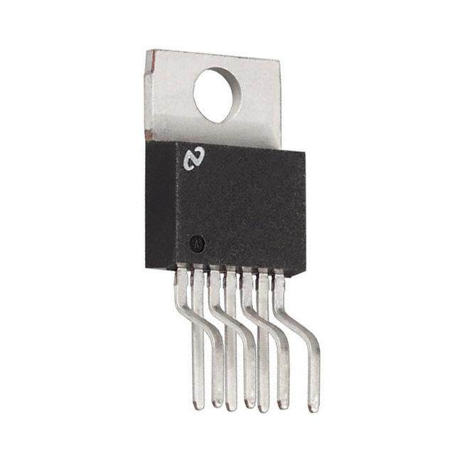
ICGOO电子元器件商城为您提供LT1076HVCT#PBF由LINEAR TECHNOLOGY设计生产,在icgoo商城现货销售,并且可以通过原厂、代理商等渠道进行代购。 LT1076HVCT#PBF价格参考。LINEAR TECHNOLOGYLT1076HVCT#PBF封装/规格:PMIC - 稳压器 - DC DC 开关稳压器, 可调式 降压,升压,反激 开关稳压器 IC 正或负 2.5V 1 输出 2A(开关) TO-220-5 成形引线。您可以下载LT1076HVCT#PBF参考资料、Datasheet数据手册功能说明书,资料中有LT1076HVCT#PBF 详细功能的应用电路图电压和使用方法及教程。
| 参数 | 数值 |
| 产品目录 | 集成电路 (IC) |
| 描述 | IC REG MULTI CONFIG ADJ TO220-5 |
| 产品分类 | |
| 品牌 | Linear Technology |
| 数据手册 | http://www.linear.com/docs/2659 |
| 产品图片 |
|
| 产品型号 | LT1076HVCT#PBF |
| PWM类型 | - |
| rohs | 无铅 / 符合限制有害物质指令(RoHS)规范要求 |
| 产品系列 | - |
| 产品目录页面 | |
| 供应商器件封装 | TO-220-5 |
| 其它名称 | LT1076HVCTPBF |
| 包装 | 管件 |
| 同步整流器 | 无 |
| 安装类型 | 通孔 |
| 封装/外壳 | TO-220-5 成形引线 |
| 工作温度 | 0°C ~ 70°C |
| 标准包装 | 50 |
| 电压-输入 | 8 V ~ 64 V |
| 电压-输出 | 2.5 V ~ 35 V |
| 电流-输出 | 2A |
| 类型 | 降压(降压),升压(升压),反相,回扫 |
| 输出数 | 1 |
| 输出类型 | 可调式 |
| 频率-开关 | 100kHz |





- 商务部:美国ITC正式对集成电路等产品启动337调查
- 曝三星4nm工艺存在良率问题 高通将骁龙8 Gen1或转产台积电
- 太阳诱电将投资9.5亿元在常州建新厂生产MLCC 预计2023年完工
- 英特尔发布欧洲新工厂建设计划 深化IDM 2.0 战略
- 台积电先进制程称霸业界 有大客户加持明年业绩稳了
- 达到5530亿美元!SIA预计今年全球半导体销售额将创下新高
- 英特尔拟将自动驾驶子公司Mobileye上市 估值或超500亿美元
- 三星加码芯片和SET,合并消费电子和移动部门,撤换高东真等 CEO
- 三星电子宣布重大人事变动 还合并消费电子和移动部门
- 海关总署:前11个月进口集成电路产品价值2.52万亿元 增长14.8%




PDF Datasheet 数据手册内容提取
LT1074/LT1076 Step-Down Switching Regulator FEATURES ponents, are included on the chip. The topology is a classic positive “buck” configuration but several design innova- ■ 5A Onboard Switch (LT1074) tions allow this device to be used as a positive-to-negative ■ Operates Up to 60V Input converter, a negative boost converter, and as a flyback ■ 100kHz Switching Frequency converter. The switch output is specified to swing 40V ■ Greatly Improved Dynamic Behavior below ground, allowing the LT1074 to drive a tapped- ■ Available in Low Cost 5 and 7-Lead Packages inductor in the buck mode with output currents up to 10A. ■ Only 8.5mA Quiescent Current The LT1074 uses a true analog multiplier in the feedback ■ Programmable Current Limit loop. This makes the device respond nearly instanta- ■ Micropower Shutdown Mode neously to input voltage fluctuations and makes loop gain independent of input voltage. As a result, dynamic behav- APPLICATIOUS ior of the regulator is significantly improved over previous designs. ■ Buck Converter with Output Voltage Range of 2.5V On-chip pulse by pulse current limiting makes the LT1074 to 50V nearly bust-proof for output overloads or shorts. The input ■ Tapped-Inductor Buck Converter with 10A Output voltage range as a buck converter is 8V to 60V, but a self- at 5V boot feature allows input voltages as low as 5V in the ■ Positive-to-Negative Converter inverting and boost configurations. ■ Negative Boost Converter ■ Multiple Output Buck Converter The LT1074 is available in low cost TO-220 or DD packages with frequency pre-set at 100kHz and current limit at 6.5A DESCRIPTIOU (LT1076 = 2.6A). A 7-pin TO-220 package is also available which allows current limit to be adjusted down to zero. In The LT®1074 is a 5A (LT1076 is rated at 2A) monolithic addition, full micropower shutdown can be programmed. bipolar switching regulator which requires only a few See Application Note 44 for design details. external parts for normal operation. The power switch, all A fixed 5V output, 2A version is also available. See LT1076-5. oscillator and control circuitry, and all current limit com- , LTC and LT are registered trademarks of Linear Technology Corporation. TYPICAL APPLICATIOU Buck Converter Efficiency Basic Positive Buck Converter LT1074 100 L1** 50µH (LT1074) VO U T = 12V, V I N = 20V 100µH (LT1076) 5V %) 90 10V TO 40V VIN VSW 5A *USE MBR340 FOR LT1076 CY ( LT1074 MBR745* R21.%18k **CPOUILLSTER EONNGICINSE##E51R00IN-02-G-15,- 25IN 2(C L(.TL 1T017047)6) FFICIEN 80 VO U T = 5V, V I N = 15V FB E 70 GND VC #PE-92114 (LT1074) #PE-92102 (LT1076) R3 R2 HURRICANE #HL-AK147QQ (LT1074) 60 L = 50µH TYPE 52 CORE 2.7k 2.21k DIODE = MBR735 + 1% + #HL-AG210LL (LT1076) C3† C2 C1 †RIPPLE CURRENT RATING ≥ IOUT/2 50 200µF 0.01µF 500µF 0 1 2 3 4 5 6 25V OUTPUT LOAD CURRENT (A) LT1074•TA01 LT1074•TPC27 sn1074 1074fds 1
LT1074/LT1076 ABSOLUTE WAXIWUW RATIUGS (Note 1) Input Voltage I Pin Voltage (Forced)............................................ 5.5V LIM LT1074/ LT1076.................................................. 45V Maximum Operating Ambient Temperature Range LT1074HV/LT1076HV ......................................... 64V Commercial.................................................0°C to 70°C Switch Voltage with Respect to Input Voltage Industrial................................................ –40°C to 85°C LT1074/ LT1076.................................................. 64V Military (OBSOLETE) .....................–55°C to 125°C LT1074HV/LT1076HV ......................................... 75V Maximum Operating Junction Temperature Range Switch Voltage with Respect to Ground Pin (V Negative) Commercial...............................................0°C to 125°C SW LT1074/LT1076 (Note 7)..................................... 35V Industrial.............................................. –40°C to 125°C LT1074HV/LT1076HV (Note 7) ........................... 45V Military (OBSOLETE) .................... –55°C to 150°C Feedback Pin Voltage.....................................–2V, +10V Maximum Storage Temperature............... –65°C to 150°C Shutdown Pin Voltage (Not to Exceed V ).............. 40V Lead Temperature (Soldering, 10 sec)......................300°C IN PACKAGE/ORDER IUFORWATIOU ORDER PART ORDER PART FRONT VIEW BOTTOM VIEW NUMBER NUMBER 5 VIN VC VIN TAB IS 4 VSW GND 3 GND LT1076CQ 1 2 LT1074CK CASE 2 VC LT1076IQ 3 IS GND LT1074HVCK 4 1 FB/SENSE LT1074MK 5-LEQA DP APCLKAASGTIEC DD FB VSW LT1074HVMK K PACKAGE LT1076CK LT1076: θJC = 4°C, θJA = 30°C/W 4-LEAD TO-3 METAL CAN LT1076HVCK LLTT11007746: :θ θJCJC = = 2 4.5°°CC, ,θ θJAJA = = 3 355°°CC/W/W LT1076MK LT1076CR FRONT VIEW OBSOLETE PACKAGE LT1076HVMK LT1076IR 7 SHDN Consider the T5 Package for Alternate Source 6 VC LT1076HVCR TAB IS 5 FB/SENSE GND 4 GND LT1076HVIR LT1074CT 3 ILIM FRONT VIEW 2 VSW LT1074HVCT 1 VIN 5 VIN R PACKAGE 4 VSW LT1074IT TAB IS 7-LEAD PLASTIC DD 3 GND LT1074HVIT GND 2 VC LT1076CT LT1076: θJC = 4°C, θJA = 30°C/W 1 FB LT1076HVCT T PACKAGE LT1074CT7 LT1076IT 5-LEAD PLASTIC TO-220 FRONT VIEW LT1074HVCT7 LEADS ARE FORMED STANDARD FOR LT1076HVIT 7 SHDN STRAIGHT LEADS, ORDER FLOW 06 6 VC LT1074IT7 TAB IS 54 FGBND LT1074HVIT7 LT1074: θJC = 2.5°C, θJA = 50°C/W GND 3 ILIM LT1076CT7 LT1076: θJC = 4°C, θJA = 50°C/W 2 VSW 1 VIN LT1076HVCT7 T7 PACKAGE 7-LEAD PLASTIC TO-220 LT1074: θJC = 2.5°C, θJA = 50°C/W LT1076: θJC = 4°C, θJA = 50°C/W *Assumes package is soldered to 0.5 IN2 of 1 oz. copper over internal ground plane or over back side plane. Consult LTC Marketing for parts specified with wider operating temperature ranges. sn1074 1074fds 2
LT1074/LT1076 ELECTRICAL CHARACTERISTICS The ● denotes the specifications which apply over the full operating temperature range, otherwise specifications are at TA = 25°C. Tj = 25°C, VIN = 25V, unless otherwise noted. PARAMETER CONDITIONS MIN TYP MAX UNITS Switch “On” Voltage (Note 2) LT1074 ISW = 1A, Tj ≥ 0°C 1.85 V ISW = 1A, Tj < 0°C 2.1 V ISW = 5A, Tj ≥ 0°C 2.3 V ISW = 5A, Tj < 0°C 2.5 V LT1076 I = 0.5A ● 1.2 V SW I = 2A ● 1.7 V SW Switch “Off” Leakage LT1074 VIN ≤ 25V, VSW = 0 5 300 µA VIN = VMAX, VSW = 0 (Note 8) 10 500 µA LT1076 VIN = 25V, VSW = 0 150 µA VIN = VMAX, VSW = 0 (Note 8) 250 µA Supply Current (Note 3) VFB = 2.5V, VIN ≤ 40V ● 8.5 11 mA 40V < V < 60V ● 9 12 mA IN VSHUT = 0.1V (Device Shutdown) (Note 9) ● 140 300 µA Minimum Supply Voltage Normal Mode ● 7.3 8 V Startup Mode (Note 4) ● 3.5 4.8 V Switch Current Limit (Note 5) LT1074 I Open ● 5.5 6.5 8.5 A LIM R = 10k (Note 6) 4.5 A LIM R = 7k (Note 6) 3 A LIM LT1076 I Open ● 2 2.6 3.2 A LIM R = 10k (Note 6) 1.8 A LIM R = 7k (Note 6) 1.2 A LIM Maximum Duty Cycle ● 85 90 % Switching Frequency 90 100 110 kHz Tj ≤ 125°C ● 85 120 kHz Tj > 125°C ● 85 125 kHz VFB = 0V through 2kΩ (Note 5) 20 kHz Switching Frequency Line Regulation 8V ≤ VIN ≤ VMAX (Note 8) ● 0.03 0.1 %/V Error Amplifier Voltage Gain (Note 7) 1V ≤ VC ≤ 4V 2000 V/V Error Amplifier Transconductance 3700 5000 8000 µmho Error Amplifier Source and Sink Current Source (VFB = 2V) 100 140 225 µA Sink (V = 2.5V) 0.7 1 1.6 mA FB Feedback Pin Bias Current VFB = VREF ● 0.5 2 µA Reference Voltage V = 2V ● 2.155 2.21 2.265 V C Reference Voltage Tolerance VREF (Nominal) = 2.21V ±0.5 ±1.5 % All Conditions of Input Voltage, Output ● ±1 ±2.5 % Voltage, Temperature and Load Current Reference Voltage Line Regulation 8V ≤ VIN ≤ VMAX (Note 8) ● 0.005 0.02 %/V V Voltage at 0% Duty Cycle 1.5 V C Over Temperature ● –4 mV/°C Multiplier Reference Voltage 24 V Shutdown Pin Current VSH = 5V ● 5 10 20 µA VSH ≤ VTHRESHOLD (≅2.5V) ● 50 µA Shutdown Thresholds Switch Duty Cycle = 0 ● 2.2 2.45 2.7 V Fully Shut Down ● 0.1 0.3 0.6 V Thermal Resistance Junction to Case LT1074 2.5 °C/W LT1076 4.0 °C/W sn1074 1074fds 3
LT1074/LT1076 ELECTRICAL CHARACTERISTICS Note 1: Absolute Maximum Ratings are those values beyond which the life Note 5: Switch frequency is internally scaled down when the feedback pin of a device may be impaired. voltage is less than 1.3V to avoid extremely short switch on times. During Note 2: To calculate maximum switch “on” voltage at currents between testing, VFB is adjusted to give a minimum switch on time of 1µs. low and high conditions, a linear interpolation may be used. R – 1k R – 1k Note 6: ILIM ≈ L I M (LT1074), ILIM ≈ L I M (LT1076). Note 3: A feedback pin voltage (VFB) of 2.5V forces the VC pin to its low 2k 5.5k clamp level and the switch duty cycle to zero. This approximates the zero Note 7: Switch to input voltage limitation must also be observed. load condition where duty cycle approaches zero. Note 8: V = 40V for the LT1074/76 and 60V for the LT1074HV/76HV. Note 4: Total voltage from VIN pin to ground pin must be ≥ 8V after start- MAX up for proper regulation. Note 9: Does not include switch leakage. BLOCK DIAGRAW INPUT SUPPLY LT1074 10 µ A 320 µ A 0.3V + µ -POWER REGU6LVATOR 6V TO ALL 500Ω SHUTDOWN AND BIAS CIRCUITRY – CURRENT LIMIT COMP + 0.04 2.35V CURRENT LIMIT C2 + SHUTDOWN 250Ω – – SHUTDOWN* I L IM * 4.5V 10k FREQ SHIFT R 100kHz R/S G1 OSCILLATOR SLATCHQ SYNC R 3V(p-p) VIN + 400Ω 15Ω + Z C1 A1 ANALOG ERROR XMULTIPLIER – AMP XY PULSE WIDTH 2.21V – Z COMPARATOR Y SWITCH OUTPUT (V S W ) FB VC 24V (EQUIVALENT) LT1076 0.1Ω *AVAILABLE ON PACKAGES WITH PIN COUNTS GREATER THAN 5. 100Ω SWITCH OUTPUT (VS W ) LT1074 • BD01 sn1074 1074fds 4
LT1074/LT1076 BLOCK DIAGRAW DESCRIPTIOU A switch cycle in the LT1074 is initiated by the oscillator voltages by feeding the FB signal into the oscillator and setting the R/S latch. The pulse that sets the latch also creating a linear frequency downshift when the FB signal locks out the switch via gate G1. The effective width of this drops below 1.3V. Current trip level is set by the voltage on pulse is approximately 700ns, which sets the maximum the I pin which is driven by an internal 320µA current LIM switch duty cycle to approximately 93% at 100kHz switch- source. When this pin is left open, it self-clamps at about ing frequency. The switch is turned off by comparator C1, 4.5V and sets current limit at 6.5A for the LT1074 and 2.6A which resets the latch. C1 has a sawtooth waveform as one for the LT1076. In the 7-pin package an external resistor input and the output of an analog multiplier as the other can be connected from the I pin to ground to set a lower LIM input. The multiplier output is the product of an internal current limit. A capacitor in parallel with this resistor will reference voltage, and the output of the error amplifier, A1, soft-start the current limit. A slight offset in C2 guarantees divided by the regulator input voltage. In standard buck that when the I pin is pulled to within 200mV of ground, LIM regulators, this means that the output voltage of A1 C2 output will stay high and force switch duty cycle to zero. required to keep a constant regulated output is indepen- The “Shutdown” pin is used to force switch duty cycle to dent of regulator input voltage. This greatly improves line zero by pulling the I pin low, or to completely shut down LIM transient response, and makes loop gain independent of the regulator. Threshold for the former is approximately input voltage. The error amplifier is a transconductance 2.35V, and for complete shutdown, approximately 0.3V. type with a G at null of approximately 5000µmho. Slew M Total supply current in shutdown is about 150µA. A 10µA current going positive is 140µA, while negative slew pull-up current forces the shutdown pin high when left current is about 1.1mA. This asymmetry helps prevent open. A capacitor can be used to generate delayed start- overshoot on start-up. Overall loop frequency compensa- up. A resistor divider will program “undervoltage lockout” tion is accomplished with a series RC network from V to C if the divider voltage is set at 2.35V when the input is at the ground. desired trip point. Switch current is continuously monitored by C2, which The switch used in the LT1074 is a Darlington NPN (single resets the R/S latch to turn the switch off if an overcurrent NPN for LT1076) driven by a saturated PNP. Special condition occurs. The time required for detection and patented circuitry is used to drive the PNP on and off very switch turn off is approximately 600ns. So minimum quickly even from the saturation state. This particular switch “on” time in current limit is 600ns. Under dead switch arrangement has no “isolation tubs” connected to shorted output conditions, switch duty cycle may have to the switch output, which can therefore swing to 40V below be as low as 2% to maintain control of output current. This ground. would require switch on time of 200ns at 100kHz switch- ing frequency, so frequency is reduced at very low output sn1074 1074fds 5
LT1074/LT1076 TYPICAL PERFORW AU CE CHARACTERISTICS V Pin Characteristics V Pin Characteristics Feedback Pin Characteristics C C 200 2.0 500 150 1.5 400 300 100 VFI C B =A D0J AUTS VTC E D= F2OVR 1.0 VF B ≥ 2.5V 200 START OF mA) 50 mA) 0.5 A)µ 100 FREQUENCY SHIFTING NT ( 0 NT ( 0 NT ( 0 RE RE RE CUR–50 SLOPE ≈ 400kΩ CUR–0.5 CUR–100 –200 –100 –1.0 V F B ≤ 2V –300 –150 –1.5 –400 –200 –2.0 –500 0 1 2 3 4 5 6 7 8 9 0 1 2 3 4 5 6 7 8 9 0 1 2 3 4 5 6 7 8 9 10 VOLTAGE (V) VOLTAGE (V) VOLTAGE (V) LT1074•TPC01 LT1074•TPC02 LT1074•TPC03 Shutdown Pin Characteristics Shutdown Pin Characteristics I Pin Characteristics LIM 40 0 100 30 –5 Tj= 25°C 50 CURRENT FLOWS OUT OF SHUTDOWN PIN 0 20 –10 Tj = 25°C –50 RENT (A)µ 100 THIS POINVTWI NMIT=OH 5V V0EIVSN RENT (A)µ––2105 STHHRUETSDHOOWLND RENT (A)µ––115000 UR–10 UR–25 UR–200 C C C –250 –20 –30 DETAILS OF THIS –300 –30 AREA SHOWN IN –35 OTHER GRAPH –350 –40 –40 –400 0 10 20 30 40 50 60 70 80 0 0.5 1.0 1.5 2.0 2.5 3.0 3.5 4.0 –2 –1 0 1 2 3 4 5 6 7 8 VOLTAGE (V) VOLTAGE (V) VOLTAGE (V) LT1074•TPC04 LT1074•PC05 LT1074•TPC06 Supply Current 20 18 16 A) 14 m T ( 12 DEVICE NOT SWITCHING EN VC = 1V RR 10 U T C 8 U NP 6 I 4 2 0 0 10 20 30 40 50 60 INPUT VOLTAGE (V) LT1074•TPC11 sn1074 1074fds 6
LT1074/LT1076 TYPICAL PERFORW AU CE CHARACTERISTICS Reference Voltage vs Supply Current (Shutdown) Temperature Switch “On” Voltage 300 2.25 3.0 2.24 Tj = 25°C 250 2.5 2.23 A) PUT CURRENT (µ112050000 VOLTAGE (V)222...222012 ON” VOLTAGE (V) 21..05 LT1074 N “ I 2.19 LT1076 1.0 50 2.18 0 2.17 0.5 0 10 20 30 40 50 60 –50 –25 0 25 50 75 100 125 150 0 1 2 3 4 5 6 INPUT VOLTAGE (V) JUNCTION TEMPERATURE (°C) SWITCH CURRENT (A) LT1074•TPC13 LT1074•TPC14 LT1074•TPC28 Reference Shift with Ripple Switching Frequency vs Voltage Error Amplifier Phase and G Temperature M 20 8k 200 120 V) 10 7k 150 115 m N REFERENCE VOLTAGE (–––––25431000000 SQWUAARVEE TRI WAVE (mho)SCONDUCTANCEµ 3456kkkk GMθ 150–00500°PHASE ()FREQUENCY (kHz)11190015050 E I AN 2k –100 90 G–60 R N T CHA–70 1k –150 85 –80 0 –200 80 0 20 40 60 80 100 120140160180200 1k 10k 100k 1M 10M –50 –25 0 25 50 75 100 125 150 PEAK-TO-PEAK RIPPLE AT FB PIN (mV) FREQUENCY (Hz) JUNCTION TEMPERATURE (°C) LT1074•TPC16 LT1074•TPC17 LT1074•TPC18 Feedback Pin Frequency Shift Current Limit vs Temperature* 160 8 140 7 I L I M PIN OPEN CY (kHz)120 MIT (A) 6 UEN100 T LI 5 R L I M = 10kΩ Q N RE 80 RE 4 F 150°C R SWITCHING 4600 –55°C 25°C OUTPUT CU 23 R L I M = 5kΩ 20 1 *MULTIPLY CURRENTS BY 0.4 FOR LT1076 0 0 0 0.5 1.0 1.5 2.0 2.5 3.0 –50 –25 0 25 50 75 100 125 150 FEEDBACK PIN VOLTAGE (V) JUNCTION TEMPERATURE (°C) LT1074•TPC19 LT1074•TPC22 sn1074 1074fds 7
LT1074/LT1076 PIU DESCRIPTIOUS V PIN IN ( )( ) ∆V V GND OUT The VIN pin is both the supply voltage for internal control ∆VOUT = 2.21 circuitry and one end of the high current switch. It is important, especially at low input voltages, that this pin be To ensure good load regulation, the ground pin must be bypassed with a low ESR, and low inductance capacitor to connected directly to the proper output node, so that no prevent transient steps or spikes from causing erratic high currents flow in this path. The output divider resistor operation. At full switch current of 5A, the switching should also be connected to this low current connection transients at the regulator input can get very large as line as shown in Figure 2. shown in Figure 1. Place the input capacitor very close to the regulator and connect it with wide traces to avoid extra inductance. Use radial lead capacitors. LT1074 FB (dl) GND (LP) dt R2 STEP = (ISW)(ESR) RAMP = (ISW)(TON) HIGH CURRENT NEGATIVE OUTPUT NODE RETURN PATH WHERE LOAD REGULATION C WILL BE MEASURED LT1074•PD01 LT1074•PD02 Figure 1. Input Capacitor Ripple Figure 2. Proper Ground Pin Connection L = Total inductance in input bypass connections FEEDBACK PIN P and capacitor. The feedback pin is the inverting input of an error amplifier “Spike” height (dI/dt • L ) is approximately 2V per which controls the regulator output by adjusting duty P inch of lead length for LT1074 and 0.8V per inch for cycle. The noninverting input is internally connected to a LT1076. trimmed 2.21V reference. Input bias current is typically 0.5µA when the error amplifier is balanced (I = 0). The “Step” for ESR = 0.05Ω and I = 5A is 0.25V. OUT SW error amplifier has asymmetrical G for large input sig- “Ramp” for C = 200µF, T = 5µs, and I = 5A, M ON SW nals to reduce startup overshoot. This makes the amplifier is 0.12V. more sensitive to large ripple voltages at the feedback pin. Input current on the VIN Pin in shutdown mode is the sum 100mVp-p ripple at the feedback pin will create a 14mV of actual supply current (≈140µA, with a maximum of offset in the amplifier, equivalent to a 0.7% output voltage 300µA), and switch leakage current. Consult factory for shift. To avoid output errors, output ripple (P-P) should be special testing if shutdown mode input current is critical. less than 4% of DC output voltage at the point where the output divider is connected. GROUND PIN See the “Error Amplifier” section for more details. It might seem unusual to describe a ground pin, but in the Frequency Shifting at the Feedback Pin case of regulators, the ground pin must be connected properly to ensure good load regulation. The internal The error amplifier feedback pin (FB) is used to downshift reference voltage is referenced to the ground pin; so any the oscillator frequency when the regulator output voltage error in ground pin voltage will be multiplied at the output; is low. This is done to guarantee that output short-circuit sn1074 1074fds 8
LT1074/LT1076 PIU DESCRIPTIOUS current is well controlled even when switch duty cycle SHUTDOWN PIN must be extremely low. Theoretical switch “on” time for a The shutdown pin is used for undervoltage lockout, micro- buck converter in continuous mode is: power shutdown, soft-start, delayed start, or as a general purpose on/off control of the regulator output. It controls V +V tON = OUT D switching action by pulling the ILIM pin low, which forces VIN•f the switch to a continuous “off” state. Full micropower shutdown is initiated when the shutdown pin drops below V = Catch diode forward voltage ( ≈ 0.5V) D 0.3V. f = Switching frequency The V/I characteristics of the shutdown pin are shown in At f = 100kHz, t must drop to 0.2µs when V = 25V ON IN Figure 4. For voltages between 2.5V and ≈V , a current of and the output is shorted (V = 0V). In current limit, IN OUT 10µA flows out of the shutdown pin. This current in- the LT1074 can reduce t to a minimum value of ON creases to ≈25µA as the shutdown pin moves through the ≈0.6µs, much too long to control current correctly for 2.35V threshold. The current increases further to ≈30µA at V = 0. To correct this problem, switching frequency OUT the 0.3V threshold, then drops to ≈15µA as the shutdown is lowered from 100kHz to 20kHz as the FB pin drops voltage fall below 0.3V. The 10µA current source is in- from 1.3V to 0.5V. This is accomplished by the circuitry cluded to pull the shutdown pin to its high or default state when left open. It also provides a convenient pull-up for TO delayed start applications with a capacitor on the shut- OSCILLATOR down pin. VOUT +2V Q1 When activated, the typical collector current of Q1 in R1 Figure 5, is ≈2mA. A soft-start capacitor on the I pin will + 2.21V R3 LIM ERROR 3k delay regulator shutdown in response to C1, by VC AMPLIFIER– EDXIVTIEDRENRAL ≈(5V)(CLIM)/2mA. Soft-start after full micropower shut- FB down is ensured by coupling C2 to Q1. R2 2.21k 0 LT1074•PD03 Tj= 25°C –5 Figure 3. Frequency Shifting CURRENT FLOWS OUT OF SHUTDOWN PIN –10 shown in Figure 3. A)–15 µ SHUTDOWN T ( THRESHOLD Q1 is off when the output is regulating (VFB = 2.21V). As REN–20 R the output is pulled down by an overload, V will eventu- U–25 FB C ally reach 1.3V, turning on Q1. As the output continues to –30 drop, Q1 current increases proportionately and lowers the –35 frequency of the oscillator. Frequency shifting starts when –40 the output is ≈ 60% of normal value, and is down to its 0 0.5 1.0 1.5 2.0 2.5 3.0 3.5 4.0 minimum value of ≅ 20kHz when the output is ≅ 20% of VOLTAGE (V) LT1074•PC05 normal value. The rate at which frequency is shifted is Figure 4. Shutdown Pin Characteristics determined by both the internal 3k resistor R3 and the external divider resistors. For this reason, R2 should not be increased to more than 4kΩ, if the LT1074 will be subjected to the simultaneous conditions of high input voltage and output short-circuit. sn1074 1074fds 9
LT1074/LT1076 PIU DESCRIPTIOUS VIN Hysteresis in undervoltage lockout may be accomplished by connecting a resistor (R3) from the I pin to the 10 µ A 300 µ A LIM shutdown pin as shown in Figure 7. D1 prevents the shutdown divider from altering current limit. SHUTDOWN – PIN ILIM C1 PIN 2.3V + R1 VIN SHUT Q1 6V EXTERNAL R3 D1* LT1074 – CLIM ILIM R2 C2 OPTIONAL CURRENT 0.3V + LIMIT RESISTOR *1N4148 LT1074•PD09 TO TOTAL REGULATOR Figure 7. Adding Hysteresis SHUTDOWN LT1074•PD07 Figure 5. Shutdown Circuitry ⎛ R1⎞ TripPoint=V =2.35V 1+ TP ⎜ ⎟ Undervoltage Lockout ⎝ R2⎠ Undervoltage lockout point is set by R1 and R2 in Figure6. If R3 is added, the lower trip point (V descending) will be IN To avoid errors due to the 10µA shutdown pin current, R2 the same. The upper trip point (V ) will be: UTP is usually set at 5k, and R1 is found from: ⎛ R1 R1⎞ ⎛R1⎞ (VTP −VSH) VUTP =VSH⎝⎜1R2+R3⎠⎟ −0.8V⎝⎜R3⎠⎟ R1=R2 V SH If R1 and R2 are chosen, R3 is given by: V = Desired undervoltage lockout voltage TP ( )( ) V = Threshold for lockout on the VSH−0.8V R1 SH R3= shutdown pin = 2.45V ⎛ R1⎞ V −V 1+ UTP SH⎜ ⎟ If quiescent supply current is critical, R2 may be increased ⎝ R2⎠ up to 15kΩ, but the denominator in the formula for R2 should replace V with V – (10µA)(R2). Example: An undervoltage lockout is required such that SH SH the output will not start until V = 20V, but will continue IN to operate until V drops to 15V. Let R2 = 2.32k. IN R1 VIN SHUT ( ) LT1074 15V−2.35V ( ) R1= 2.34k =12.5k R2 2.35V GND 5k ( )( ) 2.35−0.8 12.5 R3= =3.9k LT1074•PD08 ⎛ 12.5⎞ Figure 6. Undervoltage Lockout 20−2.35⎜1+ ⎟ ⎝ 2.32⎠ sn1074 1074fds 10
LT1074/LT1076 PIU DESCRIPTIOUS I PIN from forcing current back into the I pin. To calculate a LIM LIM value for R , first calculate R , the R : The I pin is used to reduce current limit below the FB LIM FB LIM preset value of 6.5A. The equivalent circuit for this pin is ( )( ) shown in Figure 8. ISC −0.44* RL ( ) R = R inkΩ FB ( ) L 0.5*R −1kΩ −I TO LIMIT L SC CIRCUIT VIN 320 µ A *Change 0.44 to 0.16, and 0.5 to 0.18 for LT1076. D2 Example: I = 4A, ISC = 1.5A, R = (4)(2k) + 1k = 9k Q1 LIM LIM D1 4.3V ( )( ) R1 1.5−0.44 9kΩ 8K D3 RFB = ( ) (3.8kΩ) 6V 0.5 9k−1k −1.5 I L IM LT1047•PD12 VOUT Figure 8. I Pin Circuit LIM LT1074 FB When ILIM is left open, the voltage at Q1 base clamps at 5V I L IM through D2. Internal current limit is determined by the current through Q1. If an external resistor is connected RFB D2 between I and ground, the voltage at Q1 base can be RLIM 1N4148 LIM reduced for lower current limit. The resistor will have a LT1074•PD13 voltage across it equal to (320µA)(R), limited to ≈5V when Figure 9. Foldback Current Limit clamped by D2. Resistance required for a given current limit is: Error Amplifier R = I (2kΩ) + 1kΩ (LT1074) LIM LIM The error amplifier in Figure 10 is a single stage design R = I (5.5kΩ) + 1kΩ (LT1076) with added inverters to allow the output to swing above LIM LIM and below the common mode input voltage. One side of As an example, a 3A current limit would require the amplifier is tied to a trimmed internal reference voltage 3A(2k) + 1k = 7kΩ for the LT1074. The accuracy of these of 2.21V. The other input is brought out as the FB (feed- formulas is ±25% for 2A ≤ I ≤ 5A (LT1074) and LIM back) pin. This amplifier has a G (voltage “in” to current M 7A ≤ I ≤ 1.8A (LT1076), so I should be set at least LIM LIM “out”) transfer function of ≈5000µmho. Voltage gain is 25% above the peak switch current required. determined by multiplying G times the total equivalent M Foldback current limiting can be easily implemented by output loading, consisting of the output resistance of Q4 adding a resistor from the output to the I pin as shown and Q6 in parallel with the series RC external frequency LIM in Figure 9. This allows full desired current limit (with or compensation network. At DC, the external RC is ignored, without R ) when the output is regulating, but reduces and with a parallel output impedance for Q4 and Q6 of LIM current limit under short-circuit conditions. A typical value 400kΩ, voltage gain is ≈2000. At frequencies above a few for R is 5kΩ, but this may be adjusted up or down to set hertz, voltage gain is determined by the external compen- FB the amount of foldback. D2 prevents the output voltage sation, R and C . C C sn1074 1074fds 11
LT1074/LT1076 PIU DESCRIPTIOUS 5.8V Q4 90 µ A 90 µ A Q3 50 µ A D1 VC EXTERNAL FREQUENCY Q1 Q2 FB 50 µ A COMPENSATION 90 µ A X1.8 D2 RC Q6 2.21V 140 µ A CC 300Ω ALL CURRENTS SHOWN ARE AT NULL CONDITION LT1074 • PD11 Figure 10. Error Amplifier The error amplifier has asymmetrical peak output current. G m Q3 and Q4 current mirrors are unity-gain, but the Q6 A = atmidfrequencies V 2π•f•C mirror has a gain of 1.8 at output null and a gain of 8 when C A =G •R athighfrequencies the FB pin is high (Q1 current = 0). This results in a V m C maximum positive output current of 140µA and a maxi- Phase shift from the FB pin to the VC pin is 90° at mid mum negative (sink) output current of ≅1.1mA. The asym- frequencies where the external C is controlling gain, then metry is deliberate—it results in much less regulator C drops back to 0° (actually 180° since FB is an inverting output overshoot during rapid start-up or following the input) when the reactance of C is small compared to R . release of an output overload. Amplifier offset is kept low C C The low frequency “pole” where the reactance of C is by area scaling Q1 and Q2 at 1.8:1. C equal to the output impedance of Q4 and Q6 (r ), is: O Amplifier swing is limited by the internal 5.8V supply for positive outputs and by D1 and D2 when the output goes 1 f = r ≈400kΩ low. Low clamp voltage is approximately one diode drop POLE O 2π•rO •C (≈0.7V – 2mV/°C). Although f varies as much as 3:1 due to r variations, Note that both the FB pin and the V pin have other internal POLE O C mid-frequency gain is dependent only on G , which is connections. Refer to the frequency shifting and synchro- m specified much tighter on the data sheet. The higher nizing discussions. frequency “zero” is determined solely by R and C . C C 1 f = ZERO 2π•R •C C C sn1074 1074fds 12
LT1074/LT1076 TYPICAL APPLICATIOUS Tapped-Inductor Buck Converter L2 L1* 5µH 20V† TO 3V5IVN VIN VSW 3 1 V5VO,U 1T0A† D2 LT1074HV 35V D1** R1 5W 2.8k C1 FB + 4400µF GND VC (2 EA + R1k3 D1N35819 R2.221k 21260V0)µF, + C319640VµF C3 C2 0.01µF 200µF 0.2µF 50V *PULSE ENGINEERING #PE±65282 **MOTOROLA MBR2030CTL †IF INPUT VOLTAGE IS BELOW 20V, MAXIMUM OUTPUT CURRENT WILL BE REDUCED. SEE AN44 LT1074 •TA02 Positive-to-Negative Converter with 5V Output VIN + C1 4.5V to 220µF + 40V 50V L1 25µH 5A†† R3* VIN VSW R5.11*k* 2.74k + C2 LT1074 R2** 1000µF 10k 10V GND VC VFB OPTIONAL FILTER D1† 5µH – MBR745 R4 200µF C3 C4** 1.82k* +10V 0.1µF 0.01µF –5V,1A*** * = 1% FILM RESISTORS † LOWER REVERSE VOLTAGE RATING MAY BE USED FOR LOWER INPUT VOLTAGES. D1 = MOTOROLA-MBR745 LOWER CURRENT RATING IS ALLOWED FOR LOWER OUTPUT CURRENT. SEE AN44. C1 = NICHICON-UPL1C221MRH6 †† LOWER CURRENT RATING MAY BE USED FOR LOWER OUTPUT CURRENT. SEE AN44. C2 = NICHICON-UPL1A102MRH6 L1 = COILTRONICS-CTX25-5-52 ** R1, R2, AND C4 ARE USED FOR LOOP FREQUENCY COMPENSATION WITH LOW INPUT VOLTAGE, BUT R1 AND R2 MUST BE INCLUDED IN THE CALCULATION FOR OUTPUT VOLTAGE DIVIDER VALUES. FOR HIGHER OUTPUT VOLTAGES, INCREASE R1, R2, AND R3 PROPORTIONATELY. FOR INPUT VOLTAGE > 10V, R1, R2, AND C4 CAN BE ELIMINATED, AND COMPENSATION IS DONE TOTALLY ON THE V C PIN. R3 = V O U T –2.37 (KΩ) R1 = (R3) (1.86) R2 = (R3) (3.65) ** MAXIMUM OUTPUT CURRENT OF 1A IS DETERMINED BY MINIMUM INPUT VOLTAGE OF 4.5V. HIGHER MINIMUM INPUT VOLTAGE WILL ALLOW MUCH HIGHER OUTPUT CURRENTS. SEE AN44. LT1074 • TA03 sn1074 1074fds 13
LT1074/LT1076 PACKAGE DESCRIPTIOU K Package 4-Lead TO-3 Metal Can (Reference LTC DWG # 05-08-1311) 0.760 – 0.775 0.320 – 0.350 (19.30 – 19.69) (8.13 – 8.89) 0.060 – 0.135 (1.524 – 3.429) 0.420 – 0.480 (10.67 – 12.19) 0.038 – 0.043 (0.965 – 1.09) 1.177 – 1.197 (29.90 – 30.40) 0.655 – 0.675 0.470 TP (16.64 – 19.05) P.C.D. 0.151 – 0.161 (3.84 – 4.09) DIA 2 PLC 0.167 – 0.177 (4.24 – 4.49) R 0.490 – 0.510 72° (12.45 – 12.95) 18° R K4(TO-3) 1098 OBSOLETE PACKAGE Q Package 5-Lead Plastic DD Pak (Reference LTC DWG # 05-08-1461) 0.060 (1.524) 0.390 – 0.415 0.256 0.060 TYP (9.906 – 10.541) 0.165 – 0.180 (6.502) (1.524) (4.191 – 4.572) 0.045 – 0.055 (1.143 – 1.397) 15° TYP +0.008 0.004 0.060 0.183 0.330 – 0.370 0.059 –0.004 (1.524) (4.648) (1.499) ( +0.203) (8.382 – 9.398) 0.102 TYP –0.102 0.095 – 0.115 (2.413 – 2.921) 0.075 (1.905) (07..360200) 0.143+–00..001220 (01B.0.S76C07) (00..031330 –– 00..052834) (01..025700 ±± 00..031025) BOTTOM VIEW OF DD PAK (3.632+–00..350058) (00..072181 –– 00..093685) Q(DD5) 1098 HATCHED AREA IS SOLDER PLATED COPPER HEAT SINK sn1074 1074fds 14
LT1074/LT1076 PACKAGE DESCRIPTIOU R Package 7-Lead Plastic DD Pak (Reference LTC DWG # 05-08-1462) 0.060 (1.524) 0.390 – 0.415 0.256 0.060 TYP (9.906 – 10.541) 0.165 – 0.180 (6.502) (1.524) (4.191 – 4.572) 0.045 – 0.055 (1.143 – 1.397) 15° TYP +0.008 0.004 0.060 0.183 0.330 – 0.370 0.059 –0.004 (1.524) (4.648) (1.499) ( +0.203) (8.382 – 9.398) 0.102 TYP –0.102 0.095 – 0.115 (2.413 – 2.921) 0.075 (1.905) (07..360200) 0.143+–00..001220 0.026 – 0.036 (01B.0.S25C70) (00..031330 –– 00..052834) (01..025700 ±± 00..031025) ( +0.305) BOTTOM VIEW OF DD PAK 3.632 (0.660 – 0.914) –0.508 HATCHED AREA IS SOLDER PLATED R (DD7) 1098 COPPER HEAT SINK T Package 5-Lead Plastic TO-220 (Standard) (Reference LTC DWG # 05-08-1421) 0.147 – 0.155 0.165 – 0.180 0.390 – 0.415 (3.734 – 3.937) (4.191 – 4.572) 0.045 – 0.055 (9.906 – 10.541) DIA (1.143 – 1.397) 0.230 – 0.270 (5.842 – 6.858) 0.570 – 0.620 0.620 0.460 – 0.500 (14.478 – 15.748) (15.75) (11.684 – 12.700) 0.330 – 0.370 TYP 0.700 – 0.728 (8.382 – 9.398) (17.78 – 18.491) 0.095 – 0.115 SEATING PLANE (2.413 – 2.921) 0.152 – 0.202 0.260 – 0.320 (3.861 – 5.131) 0.155 – 0.195* (3.937 – 4.953) (6.60 – 8.13) 0.013 – 0.023 (0.330 – 0.584) 0.067 BSC 0.028 – 0.038 0.135 – 0.165 (1.70) (0.711 – 0.965) (3.429 – 4.191) * MEASURED AT THE SEATING PLANE T5 (TO-220) 0399 sn1074 1074fds Information furnished by Linear Technology Corporation is believed to be accurate and reliable. 15 However, no responsibility is assumed for its use. Linear Technology Corporation makes no represen- tation that the interconnection of its circuits as described herein will not infringe on existing patent rights.
LT1074/LT1076 TYPICAL APPLICATIOU Negative Boost Converter R1 100pF 12.7k VIN VFB LT1074 R2 2.21k C3+ GND VC VSW + C1 20105µVF C2 L1 D1* 1205V00µF 0.01µF 1nF 25µH R3 750Ω VOUT –15V** VIN –5V TO –15V * MBR735 ** IOUT (MAX) = 1A TO 3A DEPENDING + ON INPUT VOLTAGE. SEE AN44 100µF 5µH OPTIONAL OUTPUT FILTER LT1074 • TA04 PACKAGE DESCRIPTIOU T7 Package 7-Lead Plastic TO-220 (Standard) (Reference LTC DWG # 05-08-1422) 0.147 – 0.155 0.165 – 0.180 0.390 – 0.415 (3.734 – 3.937) (4.191 – 4.572) 0.045 – 0.055 (9.906 – 10.541) DIA (1.143 – 1.397) 0.230 – 0.270 (5.842 – 6.858) 0.570 – 0.620 0.620 0.460 – 0.500 (14.478 – 15.748) (15.75) (11.684 – 12.700) 0.330 – 0.370 TYP 0.700 – 0.728 (8.382 – 9.398) (17.780 – 18.491) SEATING PLANE 0.095 – 0.115 (2.413 – 2.921) 0.152 – 0.202 0.155 – 0.195* 0.260 – 0.320 (3.860 – 5.130) (3.937 – 4.953) (6.604 – 8.128) 0.050 0.026 – 0.036 0.013 – 0.023 BSC(1.27) (0.660 – 0.914) 0.135 – 0.165 (0.330 – 0.584) (3.429 – 4.191) *MEASURED AT THE SEATING PLANE T7 (TO-220) 0399 RELATED PARTS PART NUMBER DESCRIPTION COMMENTS LT1375/LT1376 1.5A, 500kHz Step-Down Switching Regulators V Up to 25V, I Up to 1.25A, SO-8 IN OUT LT1374/LT1374HV 4.5A, 500kHz Step-Down Switching Regulators V Up to 25V (32V for HV), I Up to 4.25A, SO-8/DD IN OUT LT1370 6A, 500kHz High Efficiency Switching Regulator 6A/42V Internal Switch, 7-Lead DD/TO-220 LT1676 Wide Input Range, High Efficiency Step-Down Regulator V from 7.4V to 60V, I Up to 0.5A, SO-8 IN OUT LT1339 High Power Synchronous DC/DC Controller V Up to 60V, I Up to 50A, Current Mode IN OUT LT1765 3A, 1.25MHz, Step-Down Regulator V = 3V to 25V, V =1.2V, TSSOP-16E, SO8 Package IN µF sn1074 1074fds 16 Linear Technology Corporation LT/CPI 0202 1.5K REV D • PRINTED IN USA 1630 McCarthy Blvd., Milpitas, CA 95035-7417 (408) 432-1900 ● FAX: (408) 434-0507 ● www.linear.com © LINEAR TECHNOLOGY CORPORATION 1994

 Datasheet下载
