ICGOO在线商城 > 集成电路(IC) > 嵌入式 - 微控制器 > LPC2101FBD48,151

 Datasheet下载
- 型号: LPC2101FBD48,151
- 制造商: NXP Semiconductors
- 库位|库存: xxxx|xxxx
- 要求:
| 数量阶梯 | 香港交货 | 国内含税 |
| +xxxx | $xxxx | ¥xxxx |
查看当月历史价格
查看今年历史价格
LPC2101FBD48,151产品简介:
ICGOO电子元器件商城为您提供LPC2101FBD48,151由NXP Semiconductors设计生产,在icgoo商城现货销售,并且可以通过原厂、代理商等渠道进行代购。 LPC2101FBD48,151价格参考。NXP SemiconductorsLPC2101FBD48,151封装/规格:嵌入式 - 微控制器, ARM7® 微控制器 IC LPC2100 16/32-位 70MHz 8KB(8K x 8) 闪存 48-LQFP(7x7)。您可以下载LPC2101FBD48,151参考资料、Datasheet数据手册功能说明书,资料中有LPC2101FBD48,151 详细功能的应用电路图电压和使用方法及教程。
| 参数 | 数值 |
| 产品目录 | 集成电路 (IC)半导体 |
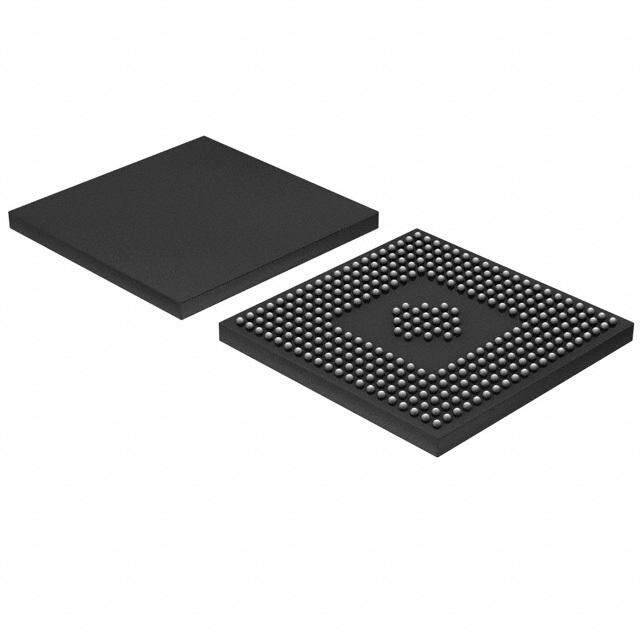
| 描述 | IC ARM7 MCU FLASH 8K 48-LQFPARM微控制器 - MCU ARM7 8KF/2KR/10BADC |
| EEPROM容量 | - |
| 产品分类 | |
| I/O数 | 32 |
| 品牌 | NXP Semiconductors |
| 产品手册 | |
| 产品图片 |
|
| rohs | 符合RoHS无铅 / 符合限制有害物质指令(RoHS)规范要求 |
| 产品系列 | 嵌入式处理器和控制器,微控制器 - MCU,ARM微控制器 - MCU,NXP Semiconductors LPC2101FBD48,151LPC2100 |
| 数据手册 | |
| 产品型号 | LPC2101FBD48,151 |
| PCN封装 | |
| RAM容量 | 2K x 8 |
| 产品培训模块 | http://www.digikey.cn/PTM/IndividualPTM.page?site=cn&lang=zhs&ptm=407http://www.digikey.cn/PTM/IndividualPTM.page?site=cn&lang=zhs&ptm=8526http://www.digikey.cn/PTM/IndividualPTM.page?site=cn&lang=zhs&ptm=8766 |
| 产品目录页面 | |
| 产品种类 | ARM微控制器 - MCU |
| 供应商器件封装 | 48-LQFP(7x7) |
| 其它名称 | 568-2092 |
| 包装 | 托盘 |
| 可编程输入/输出端数量 | 32 |
| 商标 | NXP Semiconductors |
| 商标名 | LPC |
| 处理器系列 | LPC21 |
| 外设 | POR,PWM,WDT |
| 安装风格 | SMD/SMT |
| 定时器数量 | 4 Timer |
| 封装 | Tray |
| 封装/外壳 | 48-LQFP |
| 封装/箱体 | SOT-313-2 |
| 工作温度 | -40°C ~ 85°C |
| 工作电源电压 | 1.8 V, 3.3 V |
| 工厂包装数量 | 250 |
| 振荡器类型 | 内部 |
| 接口类型 | I2C, JTAG, SPI, SSP, UART |
| 数据RAM大小 | 2 kB |
| 数据总线宽度 | 16 bit/32 bit |
| 数据转换器 | A/D 8x10b |
| 最大工作温度 | + 85 C |
| 最大时钟频率 | 70 MHz |
| 最小工作温度 | - 40 C |
| 标准包装 | 250 |
| 核心 | ARM7TDMI-S |
| 核心处理器 | ARM7® |
| 核心尺寸 | 16/32-位 |
| 片上ADC | Yes |
| 片上DAC | Without DAC |
| 电压-电源(Vcc/Vdd) | 1.65 V ~ 3.6 V |
| 程序存储器大小 | 8 kB |
| 程序存储器类型 | Flash |
| 程序存储容量 | 8KB(8K x 8) |
| 系列 | LPC2000 |
| 输入/输出端数量 | 32 I/O |
| 连接性 | I²C, Microwire, SPI, SSI, SSP, UART/USART |
| 速度 | 70MHz |
| 配用 | /product-detail/zh/FS2009USB(ARM)/483-1023-ND/3479597/product-detail/zh/OM11020/568-4310-ND/1768403/product-detail/zh/OM10041/568-4297-ND/1768390/product-detail/zh/MCB2103UME/MCB2103UME-ND/1738486/product-detail/zh/MCB2103U/MCB2103U-ND/1738485/product-detail/zh/USB-ICP-LPC2K/622-1005-ND/1133726 |
| 长度 | 7 mm |
| 零件号别名 | LPC2101FBD48-S |


- 商务部:美国ITC正式对集成电路等产品启动337调查
- 曝三星4nm工艺存在良率问题 高通将骁龙8 Gen1或转产台积电
- 太阳诱电将投资9.5亿元在常州建新厂生产MLCC 预计2023年完工
- 英特尔发布欧洲新工厂建设计划 深化IDM 2.0 战略
- 台积电先进制程称霸业界 有大客户加持明年业绩稳了
- 达到5530亿美元!SIA预计今年全球半导体销售额将创下新高
- 英特尔拟将自动驾驶子公司Mobileye上市 估值或超500亿美元
- 三星加码芯片和SET,合并消费电子和移动部门,撤换高东真等 CEO
- 三星电子宣布重大人事变动 还合并消费电子和移动部门
- 海关总署:前11个月进口集成电路产品价值2.52万亿元 增长14.8%


PDF Datasheet 数据手册内容提取
LPC2101/02/03 Single-chip 16-bit/32-bit microcontrollers; 8 kB/16 kB/32 kB flash with ISP/IAP, fast ports and 10-bit ADC Rev. 04 — 2 June 2009 Product data sheet 1. General description TheLPC2101/02/03microcontrollersarebasedona16-bit/32-bitARM7TDMI-SCPUwith real-time emulation that combines the microcontroller with 8kB, 16kB or 32kB of embedded high-speed flash memory. A 128-bit wide memory interface and a unique accelerator architecture enable 32-bit code execution at the maximum clock rate. For critical performance in interrupt service routines and DSP algorithms, this increases performance up to 30% over Thumb mode. For critical code size applications, the alternative 16-bit Thumb mode reduces code by more than 30% with minimal performance penalty. Due to their tiny size and low power consumption, the LPC2101/02/03 are ideal for applicationswhereminiaturizationisakeyrequirement.Ablendofserialcommunications interfaces ranging from multiple UARTs, SPI to SSP and two I2C-buses, combined with on-chipSRAMof2kB/4kB/8kB,makethesedevicesverywellsuitedforcommunication gateways and protocol converters. The superior performance also makes these devices suitable for use as math coprocessors. Various 32-bit and 16-bit timers, an improved 10-bitADC,PWMfeaturesthroughoutputmatchonalltimers,and32fastGPIOlineswith up to nine edge or level sensitive external interrupt pins make these microcontrollers particularly suitable for industrial control and medical systems. 2. Features 2.1 Enhanced features Enhanced features are available in parts LPC2101/02/03 labelled Revision A and higher: n Deep power-down mode with option to retain SRAM memory and/or RTC. n Three levels of flash Code Read Protection (CRP) implemented. 2.2 Key features n 16-bit/32-bit ARM7TDMI-S microcontroller in tiny LQFP48 and HVQFN48 packages. n 2kB/4kB/8kB of on-chip static RAM and 8kB/16kB/32kB of on-chip flash program memory. 128-bit wide interface/accelerator enables high-speed 70MHz operation. n ISP/IAP via on-chip bootloader software. Single flash sector or full chip erase in 100ms and programming of 256bytes in 1ms. n EmbeddedICE-RT offers real-time debugging with the on-chip RealMonitor software. n The 10-bit ADC provides eight analog inputs, with conversion times as low as 2.44m s per channel and dedicated result registers to minimize interrupt overhead. n Two 32-bit timers/external event counters with combined seven capture and seven compare channels.
LPC2101/02/03 NXP Semiconductors Single-chip 16-bit/32-bit microcontrollers n Two 16-bit timers/external event counters with combined three capture and seven compare channels. n Low power Real-Time Clock (RTC) with independent power and dedicated 32kHz clock input. n Multiple serial interfaces including two UARTs (16C550), two Fast I2C-buses (400kbit/s), SPI and SSP with buffering and variable data length capabilities. n Vectored interrupt controller with configurable priorities and vector addresses. n Up to thirty-two, 5 V tolerant fast general purpose I/O pins. n Up to 13 edge or level sensitive external interrupt pins available. n 70MHz maximum CPU clock available from programmable on-chip PLL with a possible input frequency of 10MHz to 25MHz and a settling time of 100m s. n On-chipintegratedoscillatoroperateswithanexternalcrystalintherangefrom1MHz to 25MHz. n Power saving modes include Idle mode, Power-down mode with RTC active, and Power-down mode. n Individualenable/disableofperipheralfunctionsaswellasperipheralclockscalingfor additional power optimization. n Processor wake-up from Power-down and Deep power-down (Revision A and higher) mode via external interrupt or RTC. 3. Ordering information Table 1. Ordering information Type number Package Name Description Version LPC2101FBD48 LQFP48 plastic low profile quad flat package; 48 leads; body 7· 7· 1.4mm SOT313-2 LPC2102FBD48 LQFP48 plastic low profile quad flat package; 48 leads; body 7· 7· 1.4mm SOT313-2 LPC2103FBD48 LQFP48 plastic low profile quad flat package; 48 leads; body 7· 7· 1.4mm SOT313-2 LPC2102FHN48 HVQFN48 plastic thermal enhanced very thin quad flat package; no leads; SOT619-7 48terminals; body 7· 7· 0.85 mm LPC2103FHN48 HVQFN48 plastic thermal enhanced very thin quad flat package; no leads; SOT619-7 48terminals; body 7· 7· 0.85 mm LPC2103FHN48H HVQFN48 plastic thermal enhanced very thin quad flat package; no leads; SOT778-3 48terminals; body 6· 6· 0.85 mm 3.1 Ordering options Table 2. Ordering options Type number Flash memory RAM ADC Temperature range ((cid:176) C) LPC2101FBD48 8kB 2kB 8 inputs - 40 to +85 LPC2102FBD48 16kB 4kB 8 inputs - 40 to +85 LPC2103FBD48 32kB 8kB 8 inputs - 40 to +85 LPC2102FHN48 16kB 4kB 8 inputs - 40 to +85 LPC2103FHN48 32kB 8kB 8 inputs - 40 to +85 LPC2103FHN48H 32kB 8kB 8 inputs - 40 to +85 LPC2101_02_03_4 © NXP B.V. 2009. All rights reserved. Product data sheet Rev. 04 — 2 June 2009 2 of 37
LPC2101/02/03 NXP Semiconductors Single-chip 16-bit/32-bit microcontrollers 4. Block diagram TMS TDI XTAL2VDD(3V3)VDD(1V8) TRST TCK TDO XTAL1 RST VSS LPC2101/2102/2103 TEST/DEBUG INTERFACE HIGH SPEED SYSTEM P0[31:0] GENERAL 8 kB PLL FUNCTIONS ARM7TDMI-S PURPOSE I/O BOOT ROM system AHB BRIDGE clock VECTORED INTERRUPT ARM7 local bus CONTROLLER AMBA AHB (Advanced High-performance Bus) INTERNAL MEMORY SRAM ACCELERATOR CONTROLLER 2 kB/4 kB/ 8 kB/16 kB/ AHB TO APB 8 kB SRAM 32 kB FLASH BRIDGE APB (ARM peripheral bus) SCL0, SCL1(1) EINT2 to EXTERNAL I2C-BUS SERIAL EINT0(1) INTERRUPTS INTERFACES 0 AND 1 SDA0, SDA1(1) 3 · CAP0(1) 4 · CAP1(1) 3 · CAP2(1) CAPTURE/COMPARE SCK0, SCK1(1) 3 · MAT0(1) EXTERNAL COUNTER SPI AND SSP MOSI0, MOSI1(1) 4 · MAT1(1) TIMER 0/TIMER 1/ SERIAL INTERFACES MISO0, MISO1(1) TIMER 2/TIMER 3 3 · MAT2(1) SSEL0, SSEL1(1) 4 · MAT3(1) TXD0, TXD1(1) RXD0, RXD1(1) AD0[7:0] ADC UART0/UART1 DSR1, CTS1, RTS1, DTR1 DCD1, RI1 GENERAL RTCX1 P0[31:0] PURPOSE I/O REAL-TIME CLOCK RTCX2 VBAT WATCHDOG SYSTEM CONTROL TIMER 002aab814 (1) Pins shared with GPIO. Fig 1. Block diagram LPC2101_02_03_4 © NXP B.V. 2009. All rights reserved. Product data sheet Rev. 04 — 2 June 2009 3 of 37
LPC2101/02/03 NXP Semiconductors Single-chip 16-bit/32-bit microcontrollers 5. Pinning information 5.1 Pinning 5 1 0. T D N A 0.18/CAP1.3/SDA1 0.17/CAP1.2/SCL1 0.16/EINT0/MAT0.2 0.15/RI1/EINT2 0.14/DCD1/SCK1/EI SS DDA 0.13/DTR1/MAT1.1 DD(3V3) 0.26/AD0.7 0.25/AD0.6 0.12/DSR1/MAT1.0/ P P P P P V V P V P P P 8 7 6 5 4 3 2 1 0 9 8 7 4 4 4 4 4 4 4 4 4 3 3 3 P0.19/MAT1.2/MISO1 1 36 P0.11/CTS1/CAP1.1/AD0.4 P0.20/MAT1.3/MOSI1 2 35 P0.10/RTS1/CAP1.0/AD0.3 P0.21/SSEL1/MAT3.0 3 34 P0.24/AD0.2 VBAT 4 33 P0.23/AD0.1 VDD(1V8) 5 32 P0.22/AD0.0 LPC2101FBD48 RST 6 LPC2102FBD48 31 VSSA VSS 7 LPC2103FBD48 30 P0.9/RXD1/MAT2.2 P0.27/TRST/CAP2.0 8 29 P0.8/TXD1/MAT2.1 P0.28/TMS/CAP2.1 9 28 P0.7/SSEL0/MAT2.0 P0.29/TCK/CAP2.2 10 27 DBGSEL XTAL1 11 26 RTCK XTAL2 12 25 RTCX2 3 4 5 6 7 8 9 0 1 2 3 4 1 1 1 1 1 1 1 2 2 2 2 2 002aab821 P0.0/TXD0/MAT3.1 P0.1/RXD0/MAT3.2 P0.30/TDI/MAT3.3 P0.31/TDO VDD(3V3) P0.2/SCL0/CAP0.0 VSS RTCX1 P0.3/SDA0/MAT0.0 P0.4/SCK0/CAP0.1 P0.5/MISO0/MAT0.1 P0.6/MOSI0/CAP0.2 Fig 2. Pin configuration (LQFP48) LPC2101_02_03_4 © NXP B.V. 2009. All rights reserved. Product data sheet Rev. 04 — 2 June 2009 4 of 37
LPC2101/02/03 NXP Semiconductors Single-chip 16-bit/32-bit microcontrollers 5 1 0. T D N A terminal 1 0.18/CAP1.3/SDA1 0.17/CAP1.2/SCL1 0.16/EINT0/MAT0.2 0.15/RI1/EINT2 0.14/DCD1/SCK1/EI SS DDA 0.13/DTR1/MAT1.1 DD(3V3) 0.26/AD0.7 0.25/AD0.6 0.12/DSR1/MAT1.0/ index area P P P P P V V P V P P P 8 7 6 5 4 3 2 1 0 9 8 7 4 4 4 4 4 4 4 4 4 3 3 3 P0.19/MAT1.2/MISO1 1 36 P0.11/CTS1/CAP1.1/AD0.4 P0.20/MAT1.3/MOSI1 2 35 P0.10/RTS1/CAP1.0/AD0.3 P0.21/SSEL1/MAT3.0 3 34 P0.24/AD0.2 VBAT 4 33 P0.23/AD0.1 VDD(1V8) 5 32 P0.22/AD0.0 RST 6 LPC2102FHN48 31 VSSA LPC2103FHN48 VSS 7 LPC2103FHN48H 30 P0.9/RXD1/MAT2.2 P0.27/TRST/CAP2.0 8 29 P0.8/TXD1/MAT2.1 P0.28/TMS/CAP2.1 9 28 P0.7/SSEL0/MAT2.0 P0.29/TCK/CAP2.2 10 27 DBGSEL XTAL1 11 26 RTCK XTAL2 12 25 RTCX2 3 4 5 6 7 8 9 0 1 2 3 4 1 1 1 1 1 1 1 2 2 2 2 2 P0.0/TXD0/MAT3.1 P0.1/RXD0/MAT3.2 P0.30/TDI/MAT3.3 P0.31/TDO VDD(3V3) P0.2/SCL0/CAP0.0 VSS RTCX1 P0.3/SDA0/MAT0.0 P0.4/SCK0/CAP0.1 P0.5/MISO0/MAT0.1 P0.6/MOSI0/CAP0.2 002aad918 Transparent top view Fig 3. Pin configuration (HVQFN48) LPC2101_02_03_4 © NXP B.V. 2009. All rights reserved. Product data sheet Rev. 04 — 2 June 2009 5 of 37
LPC2101/02/03 NXP Semiconductors Single-chip 16-bit/32-bit microcontrollers 5.2 Pin description Table 3. Pin description Symbol Pin Type Description P0.0 to P0.31 I/O Port0:Port0isa32-bitI/Oportwithindividualdirectioncontrolsforeachbit. A total of 31 pins of the Port 0 can be used as general purpose bidirectional digital I/Os while P0.31 is an output only pin. The operation of port 0 pins depends upon the pin function selected via the pin connect block. P0.0/TXD0/ 13[1] I/O P0.0 —General purpose input/output digital pin. MAT3.1 O TXD0 —Transmitter output for UART0. O MAT3.1 —PWM output 1 for Timer3. P0.1/RXD0/ 14[1] I/O P0.1 —General purpose input/output digital pin. MAT3.2 I RXD0 —Receiver input for UART0. O MAT3.2 —PWM output 2 for Timer3. P0.2/SCL0/ 18[2] I/O P0.2 —General purpose input/output digital pin. Output is open-drain. CAP0.0 I/O SCL0 —I2C0 clock Input/output. Open-drain output (for I2C-bus compliance). I CAP0.0 —Capture input for Timer0, channel 0. P0.3/SDA0/ 21[2] I/O P0.3 —General purpose input/output digital pin. Output is open-drain. MAT0.0 I/O SDA0 —I2C0 data input/output. Open-drain output (for I2C-bus compliance). O MAT0.0 —PWM output for Timer0, channel 0. Output is open-drain. P0.4/SCK0/ 22[1] I/O P0.4 —General purpose input/output digital pin. CAP0.1 I/O SCK0 —Serial clock for SPI0. SPI clock output from master or input to slave. I CAP0.1 —Capture input for Timer0, channel 1. P0.5/MISO0/ 23[1] I/O P0.5 —General purpose input/output digital pin. MAT0.1 I/O MISO0 —Master In Slave Out for SPI0. Data input to SPI master or data output from SPI slave. O MAT0.1 —PWM output for Timer0, channel 1. P0.6/MOSI0/ 24[1] I/O P0.6 —General purpose input/output digital pin. CAP0.2 I/O MOSI0 —Master Out Slave In for SPI0. Data output from SPI master or data input to SPI slave. I CAP0.2 —Capture input for Timer0, channel 2. P0.7/SSEL0/ 28[1] I/O P0.7 —General purpose input/output digital pin. MAT2.0 I SSEL0 —Slave Select for SPI0. Selects the SPI interface as a slave. O MAT2.0 —PWM output for Timer2, channel 0. P0.8/TXD1/ 29[1] I/O P0.8 —General purpose input/output digital pin. MAT2.1 O TXD1 —Transmitter output for UART1. O MAT2.1 —PWM output for Timer2, channel 1. P0.9/RXD1/ 30[1] I/O P0.9 —General purpose input/output digital pin. MAT2.2 I RXD1 —Receiver input for UART1. O MAT2.2 —PWM output for Timer2, channel 2. P0.10/RTS1/ 35[3] I/O P0.10 —General purpose input/output digital pin. CAP1.0/AD0.3 O RTS1 —Request to Send output for UART1. I CAP1.0 —Capture input for Timer1, channel 0. I AD0.3 —ADC 0, input 3. LPC2101_02_03_4 © NXP B.V. 2009. All rights reserved. Product data sheet Rev. 04 — 2 June 2009 6 of 37
LPC2101/02/03 NXP Semiconductors Single-chip 16-bit/32-bit microcontrollers Table 3. Pin description …continued Symbol Pin Type Description P0.11/CTS1/ 36[3] I/O P0.11 —General purpose input/output digital pin. CAP1.1/AD0.4 I CTS1 —Clear to Send input for UART1. I CAP1.1 —Capture input for Timer 1, channel 1. I AD0.4 —ADC 0, input 4. P0.12/DSR1/ 37[3] I/O P0.12 —General purpose input/output digital pin. MAT1.0/AD0.5 I DSR1 —Data Set Ready input for UART1. O MAT1.0 —PWM output for Timer1, channel 0. I AD0.5 —ADC 0, input 5. P0.13/DTR1/ 41[1] I/O P0.13 —General purpose input/output digital pin. MAT1.1 O DTR1 —Data Terminal Ready output for UART1. O MAT1.1 —PWM output for Timer1, channel 1. P0.14/DCD1/ 44[4][5] I/O P0.14 —General purpose input/output digital pin. SCK1/EINT1 I DCD1 —Data Carrier Detect input for UART1. I/O SCK1 —SerialClockforSPI1.SPIclockoutputfrommasterorinputtoslave. I EINT1 —External interrupt 1 input. P0.15/RI1/ 45[4] I/O P0.15 —General purpose input/output digital pin. EINT2 I RI1 —Ring Indicator input for UART1. I EINT2 —External interrupt 2 input. P0.16/EINT0/ 46[4] I/O P0.16 —General purpose input/output digital pin. MAT0.2 I EINT0 —External interrupt 0 input. O MAT0.2 —PWM output for Timer0, channel 2. P0.17/CAP1.2/ 47[6] I/O P0.17 —General purpose input/output digital pin. The output is not SCL1 open-drain. I CAP1.2 —Capture input for Timer1, channel 2. I/O SCL1 — I2C1 clock Input/output. This pin is an open-drain output if I2C1 function is selected in the pin connect block. P0.18/CAP1.3/ 48[6] I/O P0.18 —General purpose input/output digital pin. The output is not SDA1 open-drain. I CAP1.3 —Capture input for Timer1, channel 3. I/O SDA1 —I2C1 data Input/output. This pin is an open-drain output if I2C1 function is selected in the pin connect block. P0.19/MAT1.2/ 1[1] I/O P0.19 —General purpose input/output digital pin. MISO1 O MAT1.2 —PWM output for Timer1, channel 2. I/O MISO1 —Master In Slave Out for SSP. Data input to SSP master or data output from SSP slave. P0.20/MAT1.3/ 2[1] I/O P0.20 —General purpose input/output digital pin. MOSI1 O MAT1.3 —PWM output for Timer1, channel 3. I/O MOSI1 —Master Out Slave for SSP. Data output from SSP master or data input to SSP slave. P0.21/SSEL1/ 3[1] I/O P0.21 —General purpose input/output digital pin. MAT3.0 I SSEL1 —Slave Select for SPI1. Selects the SPI interface as a slave. O MAT3.0 —PWM output for Timer3, channel 0. LPC2101_02_03_4 © NXP B.V. 2009. All rights reserved. Product data sheet Rev. 04 — 2 June 2009 7 of 37
LPC2101/02/03 NXP Semiconductors Single-chip 16-bit/32-bit microcontrollers Table 3. Pin description …continued Symbol Pin Type Description P0.22/AD0.0 32[3] I/O P0.22 —General purpose input/output digital pin. I AD0.0 —ADC 0, input 0. P0.23/AD0.1 33[3] I/O P0.23 —General purpose input/output digital pin. I AD0.1 —ADC 0, input 1. P0.24/AD0.2 34[3] I/O P0.24 —General purpose input/output digital pin. I AD0.2 —ADC 0, input 2. P0.25/AD0.6 38[3] I/O P0.25 —General purpose input/output digital pin. I AD0.6 —ADC 0, input 6. P0.26/AD0.7 39[3] I/O P0.26 —General purpose input/output digital pin. I AD0.7 —ADC 0, input 7. P0.27/TRST/ 8[1] I/O P0.27 —General purpose input/output digital pin. CAP2.0 I TRST —Test Reset for JTAG interface. If DBGSEL is HIGH, this pin is automatically configured for use with EmbeddedICE (Debug mode). I CAP2.0 —Capture input for Timer2, channel 0. P0.28/TMS/ 9[1] I/O P0.28 —General purpose input/output digital pin. CAP2.1 I TMS —Test Mode Select for JTAG interface. If DBGSEL is HIGH, this pin is automatically configured for use with EmbeddedICE (Debug mode). I CAP2.1 —Capture input for Timer2, channel 1. P0.29/TCK/ 10[1] I/O P0.29 —General purpose input/output digital pin. CAP2.2 I TCK —TestClockforJTAGinterface.Thisclockmustbeslowerthan1⁄ ofthe 6 CPUclock(CCLK)fortheJTAGinterfacetooperate.IfDBGSELisHIGH,this pin is automatically configured for use with EmbeddedICE (Debug mode). I CAP2.2 —Capture input for Timer2, channel 2. P0.30/TDI/ 15[1] I/O P0.30 —General purpose input/output digital pin. MAT3.3 I TDI —Test Data In for JTAG interface. If DBGSEL is HIGH, this pin is automatically configured for use with EmbeddedICE (Debug mode). O MAT3.3 —PWM output 3 for Timer3. P0.31/TDO 16[1] O P0.31 —General purpose output only digital pin. O TDO —Test Data Out for JTAG interface. If DBGSEL is HIGH, this pin is automatically configured for use with EmbeddedICE (Debug mode). RTCX1 20[7][8] I Input to the RTC oscillator circuit. Input voltage must not exceed 1.8 V. RTCX2 25[7][8] O Output from the RTC oscillator circuit. RTCK 26[7] I/O Returned test clock output:Extra signal added to the JTAG port. Assists debugger synchronization when processor frequency varies. Bidirectional pin with internal pull-up. XTAL1 11 I Inputtotheoscillatorcircuitandinternalclockgeneratorcircuits.Inputvoltage must not exceed 1.8 V. XTAL2 12 O Output from the oscillator amplifier. DBGSEL 27 I Debug select: When LOW, the part operates normally. When externally pulled HIGH at reset, P0.27 to P0.31 are configured as JTAG port, and the part is in Debug mode[9]. Input with internal pull-down. RST 6 I External reset input: A LOW on this pin resets the device, causing I/O ports and peripherals to take on their default states and processor execution to begin at address 0. TTL with hysteresis, 5 Vtolerant. LPC2101_02_03_4 © NXP B.V. 2009. All rights reserved. Product data sheet Rev. 04 — 2 June 2009 8 of 37
LPC2101/02/03 NXP Semiconductors Single-chip 16-bit/32-bit microcontrollers Table 3. Pin description …continued Symbol Pin Type Description V 7, 19, 43 I Ground: 0V reference. SS V 31 I Analogground:0Vreference.Thisshouldbenominallythesamevoltageas SSA V but should be isolated to minimize noise and error. SS V 42 I Analog 3.3V power supply: This should be nominally the same voltage as DDA V but should be isolated to minimize noise and error. The level on this DD(3V3) pin also provides a voltage reference level for the ADC. V 5 I 1.8V core power supply:This is the power supply voltage for internal DD(1V8) circuitry and the on-chip PLL. V 17, 40 I 3.3V pad power supply: This is the power supply voltage for the I/O ports. DD(3V3) VBAT 4 I RTC power supply: 3.3V on this pin supplies the power to the RTC. [1] 5V tolerant (if V and V ‡ 3.0 V) pad providing digital I/O functions with TTL levels and hysteresis and 10ns slew rate control. DD(3V3) DDA [2] Open-drain 5V tolerant (if V and V ‡ 3.0 V) digital I/O I2C-bus 400kHz specification compatible pad. It requires external DD(3V3) DDA pull-up to provide an output functionality. Open-drain configuration applies to ALL functions on that pin. [3] 5V tolerant (if V and V ‡ 3.0 V) pad providing digital I/O (with TTL levels and hysteresis and 10ns slew rate control) and DD(3V3) DDA analog input function. If configured for an input function, this pad utilizes built-in glitch filter that blocks pulses shorter than 3ns. When configured as an ADC input, digital section of the pad is disabled. [4] 5Vtolerant(ifV andV ‡ 3.0V)padprovidingdigitalI/OfunctionswithTTLlevelsandhysteresisand10nsslewratecontrol. DD(3V3) DDA If configured for an input function, this pad utilizes built-in glitch filter that blocks pulses shorter than 3 ns. [5] A LOW level during reset on pin P0.14 is considered as an external hardware request to start the ISP command handler. [6] Open-drain 5V tolerant (if V and V ‡ 3.0 V) digital I/O I2C-bus 400kHz specification compatible pad. It requires external DD(3V3) DDA pull-up to provide an output functionality. Open-drain configuration applies only to I2C function on that pin. [7] Pad provides special analog functionality. [8] For lowest power consumption, pin should be left floating when the RTC is not used. [9] SeeLPC2101/02/03 User manual UM10161 for details. LPC2101_02_03_4 © NXP B.V. 2009. All rights reserved. Product data sheet Rev. 04 — 2 June 2009 9 of 37
LPC2101/02/03 NXP Semiconductors Single-chip 16-bit/32-bit microcontrollers 6. Functional description 6.1 Architectural overview The ARM7TDMI-S is a general purpose 32-bit microprocessor, which offers high performance and very low power consumption. The ARM architecture is based on Reduced Instruction Set Computer (RISC) principles, and the instruction set and related decode mechanism are much simpler than those of microprogrammed Complex Instruction Set Computers (CISC). This simplicity results in a high instruction throughput and impressive real-time interrupt response from a small and cost-effective processor core. Pipelinetechniquesareemployedsothatallpartsoftheprocessingandmemorysystems can operate continuously. Typically, while one instruction is being executed, its successor is being decoded, and a third instruction is being fetched from memory. The ARM7TDMI-S processor also employs a unique architectural strategy known as Thumb, which makes it ideally suited to high-volume applications with memory restrictions, or applications where code density is an issue. The key idea behind Thumb is that of a super-reduced instruction set. Essentially, the ARM7TDMI-S processor has two instruction sets: • The standard 32-bit ARM set. • A 16-bit Thumb set. The Thumb set’s 16-bit instruction length allows it to approach twice the density of standard ARM code while retaining most of the ARM’s performance advantage over a traditional 16-bit processor using 16-bit registers. This is possible because Thumb code operates on the same 32-bit register set as ARM code. Thumb code is able to provide up to 65% of the code size of ARM, and 160% of the performance of an equivalent ARM processor connected to a 16-bit memory system. The particular flash implementation in the LPC2101/02/03 allows for full speed execution also in ARM mode. It is recommended to program performance critical and short code sectionsinARMmode.Theimpactontheoverallcodesizewillbeminimalbutthespeed can be increased by 30% over Thumb mode. 6.2 On-chip flash program memory The LPC2101/02/03 incorporate a 8kB, 16kB or 32kB flash memory system respectively. This memory may be used for both code and data storage. Programming of theflashmemorymaybeaccomplishedinseveralways.Itmaybeprogrammedinsystem viatheserialport.Theapplicationprogrammayalsoeraseand/orprogramtheflashwhile the application is running, allowing a great degree of flexibility for data storage field firmware upgrades, etc. The entire flash memory is available for user code as the bootloader resides in a separate memory. TheLPC2101/02/03flashmemoryprovidesaminimumof100,000erase/writecyclesand 20 years of data-retention memory. LPC2101_02_03_4 © NXP B.V. 2009. All rights reserved. Product data sheet Rev. 04 — 2 June 2009 10 of 37
LPC2101/02/03 NXP Semiconductors Single-chip 16-bit/32-bit microcontrollers 6.3 On-chip static RAM On-chip static RAM may be used for code and/or data storage. The SRAM may be accessedas8-bits,16-bits,and32-bits.TheLPC2101/02/03provide2kB,4kBor8kBof static RAM. 6.4 Memory map The LPC2101/02/03 memory map incorporates several distinct regions, as shown in Figure4. In addition, the CPU interrupt vectors may be re-mapped to allow them to reside in either flash memory (the default) or on-chip static RAM. This is described inSection 6.17 “System control”. 4.0 GB 0xFFFF FFFF AHB PERIPHERALS 3.75 GB 0xF000 0000 APB PERIPHERALS 3.5 GB 0xE000 0000 3.0 GB 0xC000 0000 RESERVED ADDRESS SPACE 0x8000 0000 2.0 GB 0x7FFF FFFF BOOT BLOCK 0x7FFF E000 0x7FFF DFFF RESERVED ADDRESS SPACE 0x4000 2000 0x4000 1FFF 8 kB ON-CHIP STATIC RAM (LPC2103) 0x4000 1000 0x4000 0FFF 4 kB ON-CHIP STATIC RAM (LPC2102) 0x4000 0800 0x4000 07FF 2 kB ON-CHIP STATIC RAM (LPC2101) 1.0 GB 0x4000 0000 RESERVED ADDRESS SPACE 0x0000 8000 32 kB ON-CHIP NON-VOLATILE MEMORY 0x0000 7FFF (LPC2103) 0x0000 4000 0x0000 3FFF 16 kB ON-CHIP NON-VOLATILE MEMORY (LPC2102) 0x0000 2000 0x0000 1FFF 8 kB ON-CHIP NON-VOLATILE MEMORY (LPC2101) 0.0 GB 0x0000 0000 002aab822 Fig 4. LPC2101/02/03 memory map LPC2101_02_03_4 © NXP B.V. 2009. All rights reserved. Product data sheet Rev. 04 — 2 June 2009 11 of 37
LPC2101/02/03 NXP Semiconductors Single-chip 16-bit/32-bit microcontrollers 6.5 Interrupt controller TheVICacceptsalloftheinterruptrequestinputsandcategorizesthemasFIQ,vectored IRQ, and non-vectored IRQ as defined by programmable settings. The programmable assignmentschememeansthatprioritiesofinterruptsfromthevariousperipheralscanbe dynamically assigned and adjusted. FIQ has the highest priority. If more than one request is assigned to FIQ, the VIC combines the requests to produce the FIQ signal to the ARM processor. The fastest possibleFIQlatencyisachievedwhenonlyonerequestisclassifiedasFIQ,becausethen the FIQ service routine does not need to branch into the interrupt service routine but can run from the interrupt vector location. If more than one request is assigned to the FIQ class, the FIQ service routine will read a word from the VIC that identifies which FIQ source(s) is (are) requesting an interrupt. VectoredIRQshavethemiddlepriority.Sixteenoftheinterruptrequestscanbeassigned to this category. Any of the interrupt requests can be assigned to any of the 16 vectored IRQ slots, among which slot 0 has the highest priority and slot 15 has the lowest. Non-vectored IRQs have the lowest priority. The VIC combines the requests from all the vectored and non-vectored IRQs to produce the IRQ signal to the ARM processor. The IRQ service routine can start by reading a registerfromtheVICandjumpingthere.IfanyofthevectoredIRQsarepending,theVIC provides the address of the highest-priority requesting IRQs service routine, otherwise it providestheaddressofadefaultroutinethatissharedbyallthenon-vectoredIRQs.The default routine can read another VIC register to see what IRQs are active. 6.5.1 Interrupt sources Each peripheral device has one interrupt line connected to the Vectored Interrupt Controller,butmayhaveseveralinternalinterruptflags.Individualinterruptflagsmayalso represent more than one interrupt source. 6.6 Pin connect block The pin connect block allows selected pins of the microcontroller to have more than one function. Configuration registers control the multiplexers to allow connection between the pin and the on chip peripherals. Peripherals should be connected to the appropriate pins priortobeingactivated,andpriortoanyrelatedinterrupt(s)beingenabled.Activityofany enabled peripheral function that is not mapped to a related pin should be considered undefined. The pin control module with its pin select registers defines the functionality of the microcontroller in a given hardware environment. After reset all pins of Port 0 are configured as input with the following exceptions: If the DBGSEL pin is HIGH (Debug mode enabled), the JTAG pins will assume their JTAG functionality for use with EmbeddedICE and cannot be configured via the pin connect block. LPC2101_02_03_4 © NXP B.V. 2009. All rights reserved. Product data sheet Rev. 04 — 2 June 2009 12 of 37
LPC2101/02/03 NXP Semiconductors Single-chip 16-bit/32-bit microcontrollers 6.7 Fast general purpose parallel I/O Device pins that are not connected to a specific peripheral function are controlled by the GPIO registers. Pins may be dynamically configured as inputs or outputs. Separate registersallowsettingorclearinganynumberofoutputssimultaneously.Thevalueofthe output register may be read back, as well as the current state of the port pins. LPC2101/02/03 introduce accelerated GPIO functions over prior LPC2000 devices: • GPIO registers are relocated to the ARM local bus for the fastest possible I/O timing. • Mask registers allow treating sets of port bits as a group, leaving other bits unchanged. • All GPIO registers are byte addressable. • Entire port value can be written in one instruction. 6.7.1 Features • Bit-levelsetandclearregistersallowasingleinstructionsetorclearofanynumberof bits in one port. • Direction control of individual bits. • Separate control of output set and clear. • All I/O default to inputs after reset. 6.8 10-bit ADC TheLPC2101/02/03containoneADC.Itisasingle10-bitsuccessiveapproximationADC with eight channels. 6.8.1 Features • Measurement range of 0V to 3.3V. • Each converter capable of performing more than 400,000 10-bit samples per second. • Burst conversion mode for single or multiple inputs. • Optional conversion on transition on input pin or Timer Match signal. • Every analog input has a dedicated result register to reduce interrupt overhead. 6.9 UARTs The LPC2101/02/03 each contain two UARTs. In addition to standard transmit and receive data lines, UART1 also provides a full modem control handshake interface. Compared to previous LPC2000 microcontrollers, UARTs in LPC2101/02/03 include a fractional baud rate generator for both UARTs. Standard baud rates such as 115200 can be achieved with any crystal frequency above 2MHz. 6.9.1 Features • 16byte Receive and Transmit FIFOs. • Register locations conform to 16C550 industry standard. • Receiver FIFO trigger points at 1, 4, 8, and 14bytes LPC2101_02_03_4 © NXP B.V. 2009. All rights reserved. Product data sheet Rev. 04 — 2 June 2009 13 of 37
LPC2101/02/03 NXP Semiconductors Single-chip 16-bit/32-bit microcontrollers • Built-in fractional baud rate generator covering wide range of baud rates without a need for external crystals of particular values. • Transmission FIFO control enables implementation of software (XON/XOFF) flow control on both UARTs. • UART1 is equipped with standard modem interface signals. This module also provides full support for hardware flow control (auto-CTS/RTS). 6.10 I2C-bus serial I/O controllers The LPC2101/02/03 each contain two I2C-bus controllers. The I2C-bus is bidirectional, for inter-IC control using only two wires: a Serial Clock Line (SCL),andaSerialDataLine(SDA).Eachdeviceisrecognizedbyauniqueaddressand can operate as either a receiver-only device (e.g., LCD driver) or a transmitter with the capability to both receive and send information such as serial memory. Transmitters and/or receivers can operate in either master or slave mode, depending on whether the chiphastoinitiateadatatransferorisonlyaddressed.TheI2C-busisamulti-masterbus, it can be controlled by more than one bus master connected to it. The I2C-bus implemented in LPC2101/02/03 supports bit rates up to 400kbit/s (Fast I2C-bus). 6.10.1 Features • Compliant with standard I2C-bus interface. • Easy to configure as Master, Slave, or Master/Slave. • Programmable clocks allow versatile rate control. • Bidirectional data transfer between masters and slaves. • Multi-master bus (no central master). • Arbitration between simultaneously transmitting masters without corruption of serial data on the bus. • Serialclocksynchronizationallowsdeviceswithdifferentbitratestocommunicatevia one serial bus. • Serialclocksynchronizationcanbeusedasahandshakemechanismtosuspendand resume serial transfer. • The I2C-bus can also be used for test and diagnostic purposes. 6.11 SPI serial I/O controller The LPC2101/02/03 each contain one SPI controller. The SPI is a full duplex serial interface,designedtohandlemultiplemastersandslavesconnectedtoagivenbus.Only a single master and a single slave can communicate on the interface during a given data transfer. During a data transfer the master always sends 8bits to 16bits of data to the slave, and the slave always sends 8bits to 16bits of data to the master. 6.11.1 Features • Compliant with SPI specification. • Synchronous, Serial, Full Duplex, Communication. LPC2101_02_03_4 © NXP B.V. 2009. All rights reserved. Product data sheet Rev. 04 — 2 June 2009 14 of 37
LPC2101/02/03 NXP Semiconductors Single-chip 16-bit/32-bit microcontrollers • Combined SPI master and slave. • Maximum data bit rate of one eighth of the input clock rate. 6.12 SSP serial I/O controller TheLPC2101/02/03eachcontainoneSSP.TheSSPcontrolleriscapableofoperationon aSPI,4-wireSSI,orMicrowirebus.Itcaninteractwithmultiplemastersandslavesonthe bus.However,onlyasinglemasterandasingleslavecancommunicateonthebusduring agivendatatransfer.TheSSPsupportsfullduplextransfers,withdataframesof4bitsto 16 bits flowing from the master to the slave and from the slave to the master. Often only one of these data streams carries meaningful data. 6.12.1 Features • Compatible with Motorola SPI, 4-wire Texas Instruments SSI, and National Semiconductor’s Microwire buses • Synchronous serial communication • Master or slave operation • 8-frame FIFOs for both transmit and receive • Fourbits to 16 bits per frame 6.13 General purpose 32-bit timers/external event counters The Timer/Counter is designed to count cycles of the Peripheral Clock (PCLK) or an externally supplied clock and optionally generate interrupts or perform other actions at specified timer values, based on four match registers. It also includes four capture inputs totrapthetimervaluewhenaninputsignaltransitions,optionallygeneratinganinterrupt. Multiple pins can be selected to perform a single capture or match function, providing an application with ‘or’ and ‘and’, as well as ‘broadcast’ functions among them. The LPC2101/02/03 can count external events on one of the capture inputs if the minimumexternalpulseisequalorlongerthanaperiodofthePCLK.Inthisconfiguration, unused capture lines can be selected as regular timer capture inputs or used as external interrupts. 6.13.1 Features • A 32-bit timer/counter with a programmable 32-bit prescaler. • External event counter or timer operation. • Four 32-bit capture channels per timer/counter that can take a snapshot of the timer value when an input signal transitions. A capture event may also optionally generate an interrupt. • Four 32-bit match registers that allow: – Continuous operation with optional interrupt generation on match. – Stop timer on match with optional interrupt generation. – Reset timer on match with optional interrupt generation. • Four external outputs per timer/counter corresponding to match registers, with the following capabilities: – Set LOW on match. LPC2101_02_03_4 © NXP B.V. 2009. All rights reserved. Product data sheet Rev. 04 — 2 June 2009 15 of 37
LPC2101/02/03 NXP Semiconductors Single-chip 16-bit/32-bit microcontrollers – Set HIGH on match. – Toggle on match. – Do nothing on match. 6.14 General purpose 16-bit timers/external event counters The Timer/Counter is designed to count cycles of the peripheral clock (PCLK) or an externally supplied clock and optionally generate interrupts or perform other actions at specifiedtimervalues,basedonfourmatchregisters.Italsoincludesthreecaptureinputs totrapthetimervaluewhenaninputsignaltransitions,optionallygeneratinganinterrupt. Multiple pins can be selected to perform a single capture or match function, providing an application with ‘or’ and ‘and’, as well as ‘broadcast’ functions among them. The LPC2101/02/03 can count external events on one of the capture inputs if the minimumexternalpulseisequalorlongerthanaperiodofthePCLK.Inthisconfiguration, unused capture lines can be selected as regular timer capture inputs or used as external interrupts. 6.14.1 Features • Two 16-bit timer/counters with a programmable 16-bit prescaler. • External event counter or timer operation. • Three 16-bit capture channels that can take a snapshot of the timer value when an input signal transitions. A capture event may also optionally generate an interrupt. • Four 16-bit match registers that allow: – Continuous operation with optional interrupt generation on match. – Stop timer on match with optional interrupt generation. – Reset timer on match with optional interrupt generation. • Four external outputs per timer/counter corresponding to match registers, with the following capabilities: – Set LOW on match. – Set HIGH on match. – Toggle on match. – Do nothing on match. 6.15 Watchdog timer Thepurposeofthewatchdogistoresetthemicrocontrollerwithinareasonableamountof time if it enters an erroneous state. When enabled, the watchdog will generate a system reset if the user program fails to ‘feed’ (or reload) the watchdog within a predetermined amount of time. 6.15.1 Features • Internally resets chip if not periodically reloaded. • Debug mode. • Enabledbysoftwarebutrequiresahardwareresetorawatchdogreset/interrupttobe disabled. LPC2101_02_03_4 © NXP B.V. 2009. All rights reserved. Product data sheet Rev. 04 — 2 June 2009 16 of 37
LPC2101/02/03 NXP Semiconductors Single-chip 16-bit/32-bit microcontrollers • Incorrect/Incomplete feed sequence causes reset/interrupt if enabled. • Flag to indicate watchdog reset. • Programmable 32-bit timer with internal pre-scaler. • Selectable time period from (T · 256· 4) to (T · 232· 4) in multiples of PCLK PCLK T · 4. PCLK 6.16 Real-time clock The Real-Time Clock (RTC) is designed to provide a set of counters to measure time whennormaloridleoperatingmodeisselected.TheRTChasbeendesignedtouselittle power, making it suitable for battery powered systems where the CPU is not running continuously (Idle mode). 6.16.1 Features • Measures the passage of time to maintain a calendar and clock. • Ultra-low power design to support battery powered systems. • ProvidesSeconds,Minutes,Hours,DayofMonth,Month,Year,DayofWeek,andDay of Year. • Can use either the RTC dedicated 32kHz oscillator input or clock derived from the external crystal/oscillator input at XTAL1. The programmable reference clock divider allows fine adjustment of the RTC. • Dedicated power supply pin can be connected to a battery or the main 3.3V. 6.17 System control 6.17.1 Crystal oscillator The on-chip integrated oscillator operates with external crystal in range of 1MHz to 25MHz. The oscillator output frequency is called f and the ARM processor clock osc frequency is referred to as CCLK for purposes of rate equations, etc. f and CCLK are osc the same value unless the PLL is running and connected. Refer toSection 6.17.2 “PLL” andSection 10.1 “XTAL1 input” for additional information. 6.17.2 PLL The PLL accepts an input clock frequency in the range of 10MHz to 25MHz. The input frequency is multiplied up into the range of 10MHz to 70MHz with a Current Controlled Oscillator (CCO). The multiplier can be an integer value from 1 to 32 (in practice, the multipliervaluecannotbehigherthan6onthisfamilyofmicrocontrollersduetotheupper frequency limit of the CPU). The CCO operates in the range of 156MHz to 320MHz, so there is an additional divider in the loop to keep the CCO within its frequency range while thePLLisprovidingthedesiredoutputfrequency.Theoutputdividermaybesettodivide by2,4,8,or16toproducetheoutputclock.Sincetheminimumoutputdividervalueis2, it is insured that the PLL output has a 50% duty cycle. The PLL is turned off and bypassed following a chip reset and may be enabled by software. The program must configureandactivatethePLL,waitforthePLLtolock,andthenconnecttothePLLasa clock source. The PLL settling time is 100m s. LPC2101_02_03_4 © NXP B.V. 2009. All rights reserved. Product data sheet Rev. 04 — 2 June 2009 17 of 37
LPC2101/02/03 NXP Semiconductors Single-chip 16-bit/32-bit microcontrollers 6.17.3 Reset and wake-up timer ResethastwosourcesontheLPC2101/02/03:theRSTpinandwatchdogreset.TheRST pin is a Schmitt trigger input pin with an additional glitch filter. Assertion of chip reset by any source starts the wake-up timer (see wake-up timer description below), causing the internalchipresettoremainasserteduntiltheexternalresetisde-asserted,theoscillator is running, a fixed number of clocks have passed, and the on-chip flash controller has completed its initialization. Whentheinternalresetisremoved,theprocessorbeginsexecutingataddress0,whichis the reset vector. At that point, all of the processor and peripheral registers have been initialized to predetermined reset values. Thewake-uptimerensuresthattheoscillatorandotheranalogfunctionsrequiredforchip operation are fully functional before the processor is allowed to execute instructions. This is important at power on, all types of reset, and whenever any of the aforementioned functionsareturnedoffforanyreason.Sincetheoscillatorandotherfunctionsareturned off during Power-down and Deep power-down mode, any wake-up of the processor from the Power-down modes makes use of the wake-up timer. The wake-up timer monitors the crystal oscillator as the means of checking whether it is safe to begin code execution. When power is applied to the chip, or some event caused the chip to exit Power-down mode, some time is required for the oscillator to produce a signal of sufficient amplitude to drive the clock logic. The amount of time depends on many factors, including the rate of V ramp (in the case of power on), the type of crystal DD and its electrical characteristics (if a quartz crystal is used), as well as any other external circuitry(e.g.,capacitors),andthecharacteristicsoftheoscillatoritselfundertheexisting ambient conditions. LPC2101_02_03_4 © NXP B.V. 2009. All rights reserved. Product data sheet Rev. 04 — 2 June 2009 18 of 37
LPC2101/02/03 NXP Semiconductors Single-chip 16-bit/32-bit microcontrollers 6.17.4 Code security (Code Read Protection - CRP) This feature of the LPC2101/02/03 allows user to enable different levels of security in the systemsothataccesstotheon-chipflashanduseoftheJTAGandISPcanberestricted. When needed, CRP is invoked by programming a specific pattern into a dedicated flash location. IAP commands are not affected by the CRP. Implemented in bootloader code version 2.21 are three levels of the Code Read Protection: 1. CRP1disablesaccesstochipviatheJTAGandallowspartialflashupdate(excluding flash sector 0) using a limited set of the ISP commands. This mode is useful when CRP is required and flash field updates are needed but all sectors cannot be erased. 2. CRP2 disables access to chip via the JTAG and only allows full flash erase and update using a reduced set of the ISP commands. 3. RunninganapplicationwithlevelCRP3selectedfullydisablesanyaccesstochipvia the JTAG pins and the ISP. This mode effectively disables ISP override using P0.14 pin, too. It is up to the user’s application to provide (if needed) flash update mechanism using IAP calls or call reinvoke ISP command to enable flash update via UART0. CAUTION If level three Code Read Protection (CRP3) is selected, no future factory testing can be performed on the device. Remark:Parts LPC2101/02/03 Revision ‘-’ have CRP2 enabled only (bootloader code version 2.2). 6.17.5 External interrupt inputs TheLPC2101/02/03includeuptothreeedgeorlevelsensitiveexternalinterruptinputsas selectable pin functions. When the pins are combined, external events can be processed as three independent interrupt signals. The external interrupt inputs can optionally be used to wake-up the processor from Power-down mode and Deep power-down mode. Additionally all 10 capture input pins can also be used as external interrupts without the option to wake the device up from Power-down mode. 6.17.6 Memory mapping control The memory mapping control alters the mapping of the interrupt vectors that appear beginning at address 0x00000000. Vectors may be mapped to the bottom of the on-chip flash memory, or to the on-chip static RAM. This allows code running in different memory spaces to have control of the interrupts. 6.17.7 Power control The LPC2101/02/03 supports three reduced power modes: Idle mode, Power-down mode, and Deep power-down mode. LPC2101_02_03_4 © NXP B.V. 2009. All rights reserved. Product data sheet Rev. 04 — 2 June 2009 19 of 37
LPC2101/02/03 NXP Semiconductors Single-chip 16-bit/32-bit microcontrollers InIdlemode,executionofinstructionsissuspendeduntileitheraresetorinterruptoccurs. Peripheral functions continue operation during Idle mode and may generate interrupts to cause the processor to resume execution. Idle mode eliminates power used by the processor itself, memory systems and related controllers, and internal buses. InPower-downmode,theoscillatorisshutdownandthechipreceivesnointernalclocks. The processor state and registers, peripheral registers, and internal SRAM values are preserved throughout Power-down mode and the logic levels of chip output pins remain static.ThePower-downmodecanbeterminatedandnormaloperationresumedbyeither a reset or certain specific interrupts that are able to function without clocks. Since all dynamic operation of the chip is suspended, Power-down mode reduces chip power consumption to nearly zero. Selecting an external 32kHz clock instead of the PCLK as a clock-source for the on-chip RTC will enable the microcontroller to have the RTC active during Power-down mode. Power-downcurrentisincreasedwithRTCactive.However,itissignificantlylowerthanin Idle mode. InDeep-powerdownmodeallpowerisremovedfromtheinternalchiplogicexceptforthe RTC module, the I/O ports, the SRAM, and the 32 kHz external oscillator. For additional power savings, SRAM and the 32 kHz oscillator can be powered down individually. The Deep power-down mode produces the lowest possible power consumption without actually removing power from the entire chip. In Deep power-down mode, the contents of registers and memory are not preserved except for SRAM, if selected, and three general purpose registers. Therefore, to resume operations, a full chip reset process is required. ApowerselectormoduleswitchestheRTCpowersupplyfromVBATtoV whenever DD(1V8) the core voltage is present on pin V to conserve battery power. DD(1V8) Apowercontrolforperipheralsfeatureallowsindividualperipheralstobeturnedoffifthey are not needed in the application, resulting in additional power savings during Active and Idle mode. 6.17.8 APB TheAPBdividerdeterminestherelationshipbetweentheprocessorclock(CCLK)andthe clockusedbyperipheraldevices(PCLK).TheAPBdividerservestwopurposes.Thefirst is to provide peripherals with the desired PCLK via APB so that they can operate at the speed chosen for the ARM processor. In order to achieve this, the APB may be slowed down to1⁄ to1⁄ of the processor clock rate. Because the APB must work properly at 2 4 power-up(anditstimingcannotbealteredifitdoesnotworksincetheAPBdividercontrol registersresideontheAPB),thedefaultconditionatresetisfortheAPBtorunat1⁄ ofthe 4 processor clock rate. The second purpose of the APB divider is to allow power savings when an application does not require any peripherals to run at the full processor rate. BecausetheAPBdividerisconnectedtothePLLoutput,thePLLremainsactive(ifitwas running) during Idle mode. 6.18 Emulation and debugging The LPC2101/02/03 support emulation and debugging via a JTAG serial port. LPC2101_02_03_4 © NXP B.V. 2009. All rights reserved. Product data sheet Rev. 04 — 2 June 2009 20 of 37
LPC2101/02/03 NXP Semiconductors Single-chip 16-bit/32-bit microcontrollers 6.18.1 EmbeddedICE Standard ARM EmbeddedICE logic provides on-chip debug support. The debugging of the target system requires a host computer running the debugger software and an EmbeddedICE protocol converter. The EmbeddedICE protocol converter converts the remote debug protocol commands to the JTAG data needed to access the ARM core. The ARM core has a debug communication channel function built-in. The debug communication channel allows a program running on the target to communicate with the host debugger or another separate host without stopping the program flow or even entering the debug state. The debug communication channel is accessed as a coprocessor 14 by the program running on the ARM7TDMI-S core. The debug communication channel allows the JTAG port to be used for sending and receiving data without affecting the normal program flow. The debug communication channel data and control registers are mapped in to addresses in the EmbeddedICE logic. The JTAG clock (TCK) must be slower than1⁄ of the CPU clock (CCLK) for the JTAG interface to operate. 6 6.18.2 RealMonitor RealMonitor is a configurable software module, developed by ARM Inc., which enables real time debug. It is a lightweight debug monitor that runs in the background while users debugtheirforegroundapplication.ItcommunicateswiththehostusingtheDCC,whichis presentintheEmbeddedICElogic.TheLPC2101/02/03containaspecificconfigurationof RealMonitor software programmed into the on-chip boot ROM memory. LPC2101_02_03_4 © NXP B.V. 2009. All rights reserved. Product data sheet Rev. 04 — 2 June 2009 21 of 37
LPC2101/02/03 NXP Semiconductors Single-chip 16-bit/32-bit microcontrollers 7. Limiting values Table 4. Limiting values In accordance with the Absolute Maximum Rating System (IEC 60134).[1] Symbol Parameter Conditions Min Max Unit V supply voltage (1.8V) [2] - 0.5 +2.5 V DD(1V8) V supply voltage (3.3V) [3] - 0.5 +4.6 V DD(3V3) V analog 3.3V pad supply voltage - 0.5 +4.6 V DDA V input voltage on pin VBAT for the RTC - 0.5 +4.6 V i(VBAT) V analog input voltage [4] - 0.5 +5.1 V IA V input voltage 5V tolerant I/O [5][6] - 0.5 +6.0 V I pins other I/O pins [5] - 0.5 V + 0.5[7] V DD I supply current [8] - 100[9] mA DD I ground current [10] - 100[9] mA SS T storage temperature [11] - 65 +150 (cid:176) C stg P total power dissipation (per package) based on package - 1.5 W tot(pack) heat transfer, not device power consumption V electrostatic discharge voltage Human Body - 4000 +4000 V[12] ESD Model (HBM) Machine Model - 200 +200 V[13] (MM) Charged Device - 800 +800 V[14] Model (CDM) [1] The following applies to the limiting values: a) This product includes circuitry specifically designed for the protection of its internal devices from the damaging effects of excessive staticcharge.Nonetheless,itissuggestedthatconventionalprecautionsbetakentoavoidapplyinggreaterthantheratedmaximum. b) Parameters are valid over operating temperature range unless otherwise specified. All voltages are with respect to V unless SS otherwise noted. [2] Core and internal rail. [3] External rail. [4] On ADC related pins. [5] Including voltage on outputs in 3-state mode. [6] Only valid when the V supply voltage is present. DD(3V3) [7] Not to exceed 4.6V. [8] Per supply pin. [9] The peak current is limited to 25 times the corresponding maximum current. [10] Per ground pin. [11] Dependent on package type. [12] Performed per AEC-Q100-002. [13] Performed per AEC-Q100-003. [14] Performed per AEC-Q100-011. LPC2101_02_03_4 © NXP B.V. 2009. All rights reserved. Product data sheet Rev. 04 — 2 June 2009 22 of 37
LPC2101/02/03 NXP Semiconductors Single-chip 16-bit/32-bit microcontrollers 8. Static characteristics Table 5. Static characteristics T =- 40(cid:176) C to +85(cid:176) C for commercial applications, unless otherwise specified. amb Symbol Parameter Conditions Min Typ[1] Max Unit V supply voltage [2] 1.65 1.8 1.95 V DD(1V8) (1.8V) V supply voltage [3] 2.6[4] 3.3 3.6 V DD(3V3) (3.3V) V analog 3.3V pad 2.6[5] 3.3 3.6 V DDA supply voltage V inputvoltageonpin 2.0[6] 3.3 3.6 V i(VBAT) VBAT Standard port pins,RST, RTCK I LOW-level input V =0V; no pull-up - - 3 m A IL I current I HIGH-level input V =V ; no pull-down - - 3 m A IH I DD(3V3) current I OFF-state output V =0V, V =V ; no - - 3 m A OZ O O DD(3V3) current pull-up/down I I/O latch-up current - (0.5V ) < V < (1.5V ); - - 100 mA latch DD(3V3) I DD(3V3) T < 125(cid:176) C j V input voltage pin configured to provide a digital [7][8] 0 - 5.5 V I function; V and V ‡ 3.0 V [9] DD(3V3) DDA pin configured to provide a digital [7][8] 0 V V DD(3V3) function; V and V < 3.0 V [9] DD(3V3) DDA V output voltage output active 0 - V V O DD(3V3) V HIGH-level input 2.0 - - V IH voltage V LOW-level input - - 0.8 V IL voltage V hysteresis voltage 0.4 - - V hys V HIGH-level output I =- 4mA [10] V - 0.4 - - V OH OH DD(3V3) voltage V LOW-level output I =- 4mA [10] - - 0.4 V OL OL voltage I HIGH-level output V =V - 0.4V [10] - 4 - - mA OH OH DD(3V3) current I LOW-level output V =0.4V [10] 4 - - mA OL OL current I HIGH-level V =0V [11] - - - 45 mA OHS OH short-circuit output current I LOW-level V =V [11] - - 50 mA OLS OL DDA short-circuit output current I pull-down current V =5V[12] 10 50 150 m A pd I LPC2101_02_03_4 © NXP B.V. 2009. All rights reserved. Product data sheet Rev. 04 — 2 June 2009 23 of 37
LPC2101/02/03 NXP Semiconductors Single-chip 16-bit/32-bit microcontrollers Table 5. Static characteristics …continued T =- 40(cid:176) C to +85(cid:176) C for commercial applications, unless otherwise specified. amb Symbol Parameter Conditions Min Typ[1] Max Unit I pull-up current V =0V [13] - 15 - 50 - 85 m A pu I V <V <5V[12] 0 0 0 m A DD(3V3) I I core supply current Active mode; DD(CORE) code while(1){} executed from flash; all peripherals enabledviaPCONPregisterbutnot configured to run; CCLK=70MHz V =1.8V; T =25(cid:176) C - 41 70 mA DD(1V8) amb Power-down mode; V =1.8V; T =25(cid:176) C - 2.5 25 m A DD(1V8) amb V =1.8V; T =85(cid:176) C - 35 105 m A DD(1V8) amb Deep power-down mode; RTCoff;SRAM off; T =25(cid:176) C amb V =3.3V; V =1.8V - 0.7 - m A i(VBAT) DD(1V8) I battery supply Active mode; CCLK=70MHz; BAT current PCLK=17.5MHz; PCLKenabledtoRTCK; RTCclock=32kHz (fromRTCX pins); T =25(cid:176) C [14] amb V =1.8V; V =3.0V - 10 15 m A DD(1V8) i(VBAT) Power-down mode; RTCclock=32kHz (fromRTCXpins); T =25(cid:176) C amb V =1.8V; V =2.5V - 7 12 m A DD(1V8) i(VBAT) V =1.8V; V =3.0V - 8 12 m A DD(1V8) i(VBAT) Deep power-down mode; RTCoff;SRAM off; T =25(cid:176) C amb V =1.8V; V =3.0V - 8 - m A DD(1V8) i(VBAT) I2C-bus pins V HIGH-level input 0.7V - - V IH DD(3V3) voltage V LOW-level input - - 0.3V V IL DD(3V3) voltage V hysteresis voltage - 0.5V - V hys DD(3V3) V LOW-level output I =3mA [10] - - 0.4 V OL OLS voltage I input leakage V =V - 2 4 m A LI I DD(3V3) current V =5V [15] - 10 22 m A I Oscillator pins V inputvoltageonpin 0 - 1.8 V i(XTAL1) XTAL1 LPC2101_02_03_4 © NXP B.V. 2009. All rights reserved. Product data sheet Rev. 04 — 2 June 2009 24 of 37
LPC2101/02/03 NXP Semiconductors Single-chip 16-bit/32-bit microcontrollers Table 5. Static characteristics …continued T =- 40(cid:176) C to +85(cid:176) C for commercial applications, unless otherwise specified. amb Symbol Parameter Conditions Min Typ[1] Max Unit V output voltage on 0 - 1.8 V o(XTAL2) pin XTAL2 V inputvoltageonpin 0 - 1.8 V i(RTCX1) RTCX1 V output voltage on 0 - 1.8 V o(RTCX2) pin RTCX2 [1] Typical ratings are not guaranteed. The values listed are at room temperature (25(cid:176) C), nominal supply voltages. [2] Core and internal rail. [3] External rail. [4] If V < 3.0 V, the I/O pins are not 5 V tolerant, and the ADC input voltage is limited to V = 3.0 V. DD(3V3) DDA [5] If V < 3.0 V, the I/O pins are not 5 V tolerant. DDA [6] The RTC typically fails when V drops below 1.6V. i(VBAT) [7] Including voltage on outputs in 3-state mode. [8] V supply voltages must be present. DD(3V3) [9] 3-state outputs go into 3-state mode when V is grounded. DD(3V3) [10] Accounts for 100mV voltage drop in all supply lines. [11] Allowed as long as the current limit does not exceed the maximum current allowed by the device. [12] Minimum condition for V =4.5V, maximum condition for V =5.5V. V ‡ 3.0 V and V ‡ 3.0 V. I I DDA DD(3V3) [13] Applies to P0.25:16. [14] Battery supply current on pin VBAT. [15] Input leakage current to V . SS Table 6. ADC static characteristics V =2.5V to 3.6V; T =- 40(cid:176) C to +85(cid:176) C unless otherwise specified. ADC frequency 4.5MHz. DDA amb Symbol Parameter Conditions Min Typ Max Unit V analog input voltage 0 - V V IA DDA C analog input capacitance - - 1 pF ia E differential linearity error [1][2][3] - - – 1 LSB D E integral non-linearity [1][4] - - – 2 LSB L(adj) E offset error [1][5] - - – 3 LSB O E gain error [1][6] - - – 0.5 % G E absolute error [1][7] - - – 4 LSB T [1] Conditions: V =0V, V =3.3V and V = 3.3 V for 10-bit resolution at full speed; V = 2.6 V, V = 2.6 V for 8-bit SSA DDA DD(3V3) DDA DD(3V3) resolution at full speed. [2] The ADC is monotonic, there are no missing codes. [3] The differential linearity error (E ) is the difference between the actual step width and the ideal step width. SeeFigure5. D [4] The integral non-linearity (E ) is the peak difference between the center of the steps of the actual and the ideal transfer curve after L(adj) appropriate adjustment of gain and offset errors. SeeFigure5. [5] The offset error (E ) is the absolute difference between the straight line which fits the actual curve and the straight line which fits the O ideal curve. SeeFigure5. [6] The gain error (E ) is the relative difference in percent between the straight line fitting the actual transfer curve after removing offset G error, and the straight line which fits the ideal transfer curve. SeeFigure5. [7] Theabsoluteerror(E )isthemaximumdifferencebetweenthecenterofthestepsoftheactualtransfercurveofthenon-calibratedADC T and the ideal transfer curve. SeeFigure5. LPC2101_02_03_4 © NXP B.V. 2009. All rights reserved. Product data sheet Rev. 04 — 2 June 2009 25 of 37
LPC2101/02/03 NXP Semiconductors Single-chip 16-bit/32-bit microcontrollers offset gain error error EO EG 1023 1022 1021 1020 1019 1018 (2) 7 code (1) out 6 5 (5) 4 (4) 3 (3) 2 1 1 LSB (ideal) 0 1 2 3 4 5 6 7 1018 1019 1020 1021 1022 1023 1024 VIA (LSBideal) offset error EO VDDA - VSSA 1 LSB = 1024 002aac046 (1) Example of an actual transfer curve. (2) The ideal transfer curve. (3) Differential linearity error (E ). D (4) Integral non-linearity (E ). L(adj) (5) Center of a step of the actual transfer curve. Fig 5. ADC conversion characteristics LPC2101_02_03_4 © NXP B.V. 2009. All rights reserved. Product data sheet Rev. 04 — 2 June 2009 26 of 37
LPC2101/02/03 NXP Semiconductors Single-chip 16-bit/32-bit microcontrollers 8.1 Power consumption in Deep power-down mode 002aae680 1.5 IDD(CORE) (m A) 1.25 1 VDD(1V8) =1.8 V 1.7 V 0.75 1.65 V 0.5 - 40 - 15 10 35 60 85 Temperature ((cid:176)C) Test conditions: Deep power-down mode entered; RTC off; SRAM off; V = V = V = 3.3 V. i(VBAT) DD(3V3) DDA Fig 6. Core supply current I measured at different temperatures and supply DD(CORE) voltages 002aae681 15 IBAT RTC on; SRAM on (m A) RTC on; SRAM off 12.5 10 RTC off; SRAM on RTC off; SRAM off 7.5 5 - 40 - 15 10 35 60 85 Temperature ((cid:176)C) Test conditions: Deep power-down mode entered; V = 3.3 V; V = 1.8 V; i(BAT) DD(1V8) V =V =3.3V. DD(3V3) DDA Fig 7. Battery supply current I measured at different temperatures and conditions BAT LPC2101_02_03_4 © NXP B.V. 2009. All rights reserved. Product data sheet Rev. 04 — 2 June 2009 27 of 37
LPC2101/02/03 NXP Semiconductors Single-chip 16-bit/32-bit microcontrollers 002aae682 0.20 IDD(IO) (m A) 0.15 0.10 0.05 0 - 40 - 15 10 35 60 85 Temperature ((cid:176)C) Test conditions: Deep power-down mode entered; RTC off; SRAM off; V =3.3V; DD(3V3) V =1.8V; V =V =3.3V. DD(1V8) i(BAT) DDA Fig 8. I/O supply current I measured at different temperatures DD(IO) LPC2101_02_03_4 © NXP B.V. 2009. All rights reserved. Product data sheet Rev. 04 — 2 June 2009 28 of 37
LPC2101/02/03 NXP Semiconductors Single-chip 16-bit/32-bit microcontrollers 9. Dynamic characteristics Table 7. Dynamic characteristics T =0(cid:176) Cto70(cid:176) C for commercial applications,- 40(cid:176) C to +85(cid:176) C for industrial applications, V , V over amb DD(1V8) DD(3V3) specified ranges[1]. Symbol Parameter Conditions Min Typ[2] Max Unit External clock f oscillator frequency 10 - 25 MHz osc T clock cycle time 40 - 100 ns cy(clk) t clock HIGH time T · 0.4 - - ns CHCX cy(clk) t clock LOW time T · 0.4 - - ns CLCX cy(clk) t clock rise time - - 5 ns CLCH t clock fall time - - 5 ns CHCL Port pins (except P0.2 and P0.3) t output rise time - 10 - ns r(o) t output fall time - 10 - ns f(o) I2C-bus pins (P0.2 and P0.3) t output fall time V to V 20 + 0.1· C [3] - - ns f(o) IH IL b [1] Parameters are valid over operating temperature range unless otherwise specified. [2] Typical ratings are not guaranteed. The values listed are at room temperature (25(cid:176) C), nominal supply voltages. [3] Bus capacitance C in pF, from 10pF to 400pF. b 10. Application information 10.1 XTAL1 input Theinputvoltagetotheon-chiposcillatorsislimitedto1.8V.Iftheoscillatorisdrivenbya clockinslavemode,itisrecommendedthattheinputbecoupledthroughacapacitorwith C = 100 pF. To limit the input voltage to the specified range, choose an additional i capacitortogroundC whichattenuatestheinputvoltagebyafactorC/(C +C ).Inslave g i i g mode, a minimum of 200 mV (RMS) is needed. For more details see theLPC2101/02/03 User manual UM10161. LPC2xxx XTAL1 Ci Cg 100 pF 002aae718 Fig 9. Slave mode operation of the on-chip oscillator LPC2101_02_03_4 © NXP B.V. 2009. All rights reserved. Product data sheet Rev. 04 — 2 June 2009 29 of 37
LPC2101/02/03 NXP Semiconductors Single-chip 16-bit/32-bit microcontrollers 10.2 XTAL and RTC Printed Circuit Board (PCB) layout guidelines The crystal should be connected on the PCB as close as possible to the oscillator input and output pins of the chip. Take care that the load capacitors C and C , and C in x1 x2 x3 case of third overtone crystal usage, have a common ground plane. The external components must also be connected to the ground plain. Loops must be made as small as possible, in order to keep the noise coupled in via the PCB as small as possible. Also parasitics should stay as small as possible. Values of C and C should be chosen x1 x2 smaller accordingly to the increase in parasitics of the PCB layout. LPC2101_02_03_4 © NXP B.V. 2009. All rights reserved. Product data sheet Rev. 04 — 2 June 2009 30 of 37
LPC2101/02/03 NXP Semiconductors Single-chip 16-bit/32-bit microcontrollers 11. Package outline LQFP48: plastic low profile quad flat package; 48 leads; body 7 x 7 x 1.4 mm SOT313-2 c y X 36 25 A 37 24 ZE e E HE A A2 A1 (A 3 ) wM q pin 1 index bp Lp 48 13 L detail X 1 12 ZD vM A e wM bp D B HD v M B 0 2.5 5 mm scale DIMENSIONS (mm are the original dimensions) A UNIT max. A1 A2 A3 bp c D(1) E(1) e HD HE L Lp v w y ZD(1) ZE(1) q mm 1.6 00..2005 11..4355 0.25 00..2177 00..1182 76..19 76..19 0.5 98..1855 98..1855 1 00..7455 0.2 0.12 0.1 00..9555 00..9555 70oo Note 1. Plastic or metal protrusions of 0.25 mm maximum per side are not included. OUTLINE REFERENCES EUROPEAN ISSUE DATE VERSION IEC JEDEC JEITA PROJECTION 00-01-19 SOT313-2 136E05 MS-026 03-02-25 Fig 10. Package outline SOT313-2 (LQFP48) LPC2101_02_03_4 © NXP B.V. 2009. All rights reserved. Product data sheet Rev. 04 — 2 June 2009 31 of 37
LPC2101/02/03 NXP Semiconductors Single-chip 16-bit/32-bit microcontrollers HVQFN48: plastic thermal enhanced very thin quad flat package; no leads; 48 terminals; body 7 x 7 x 0.85 mm SOT619-7 D B A terminal 1 index area E A A1 c detail X e1 C e 1/2 e b v M C A B y1C y w M C 13 24 L 25 12 e Eh e2 1/2 e 1 36 terminal 1 index area 48 37 Dh X 0 2.5 5 mm scale DIMENSIONS (mm are the original dimensions) UNIT m Aa(x1) A1 b c D(1) Dh E(1) Eh e e1 e2 L v w y y1 0.05 0.30 7.1 3.45 7.1 3.45 0.5 mm 1 0.2 0.5 5.5 5.5 0.1 0.05 0.05 0.1 0.00 0.18 6.9 3.15 6.9 3.15 0.3 Note 1. Plastic or metal protrusions of 0.075 mm maximum per side are not included OUTLINE REFERENCES EUROPEAN ISSUE DATE VERSION IEC JEDEC JEITA PROJECTION 05-10-24 SOT619-7 - - - MO-220 - - - 05-10-25 Fig 11. Package outline SOT619-7 (HVQFN48) LPC2101_02_03_4 © NXP B.V. 2009. All rights reserved. Product data sheet Rev. 04 — 2 June 2009 32 of 37
LPC2101/02/03 NXP Semiconductors Single-chip 16-bit/32-bit microcontrollers HVQFN48: plastic thermal enhanced very thin quad flat package; no leads; 48 terminals; body 6 x 6 x 0.85 mm SOT778-3 D B A terminal 1 index area E A A1 c detail X C e1 e 1/2 e b v M C A B y1C y w M C 13 24 L 25 12 e Eh e2 1/2 e 1 36 terminal 1 index area 48 37 X Dh 0 2.5 5 mm scale DIMENSIONS (mm are the original dimensions) UNIT m Aa(x1) A1 b c D(1) Dh E(1) Eh e e1 e2 L v w y y1 0.05 0.25 6.1 3.95 6.1 3.95 0.5 mm 1 0.2 0.4 4.4 4.4 0.1 0.05 0.05 0.1 0.00 0.15 5.9 3.65 5.9 3.65 0.3 Note 1. Plastic or metal protrusions of 0.075 mm maximum per side are not included OUTLINE REFERENCES EUROPEAN ISSUE DATE VERSION IEC JEDEC JEITA PROJECTION 04-06-16 SOT778-3 - - - - - - - - - 04-06-23 Fig 12. Package outline SOT778-3 (HVQFN48) LPC2101_02_03_4 © NXP B.V. 2009. All rights reserved. Product data sheet Rev. 04 — 2 June 2009 33 of 37
LPC2101/02/03 NXP Semiconductors Single-chip 16-bit/32-bit microcontrollers 12. Abbreviations Table 8. Acronym list Acronym Description ADC Analog-to-Digital Converter AMBA Advanced Microcontroller Bus Architecture APB Advanced Peripheral Bus DCC Debug Communications Channel DSP Digital Signal Processor FIFO First In, First Out FIQ Fast Interrupt reQuest GPIO General Purpose Input/Output IAP In-Application Programming IRQ Interrupt Request ISP In-System Programming PLL Phase-Locked Loop PWM Pulse Width Modulator SPI Serial Peripheral Interface SRAM Static Random Access Memory SSI Synchronous Serial Interface SSP Synchronous Serial Port TTL Transistor-Transistor Logic UART Universal Asynchronous Receiver/Transmitter VIC Vectored Interrupt Controller LPC2101_02_03_4 © NXP B.V. 2009. All rights reserved. Product data sheet Rev. 04 — 2 June 2009 34 of 37
LPC2101/02/03 NXP Semiconductors Single-chip 16-bit/32-bit microcontrollers 13. Revision history Table 9. Revision history Document ID Release date Data sheet status Change Supersedes notice LPC2101_02_03_4 20090602 Product data sheet LPC2101_02_03_3 Modifications: • Section 6.17.4 “Code security (Code Read Protection - CRP)”: added description of three CRP levels (applicable to Revision A and higher). • Section 6.17.7 “Power control”: added description of Deep power-down mode (applicable to Revision A and higher). • Section 10.1 “XTAL1 input” added. • Section 10.2 “XTAL and RTC Printed Circuit Board (PCB) layout guidelines” added. • Figure6,Figure7,Figure8: added power consumption data for Deep power-down mode (applicable to Revision A and higher). • Table3: added table note 7. • Table3:modifieddescriptionofP0.14,RTCX1,RTCX2,XTAL1,XTAL2,JTAG,andDBGSEL pins. • Table4: modified value for V . DD(3V3) • Table5: added and modified values for V . hys • Table5: Voltage range for pins V and V extended to 2.6 V. DD(3V3) DDA LPC2101_02_03_3 20081007 Product data sheet - LPC2101_02_03_2 Modifications: • Updated data sheet status to Product data sheet. • Table1 and Table2: added LPC2102FHN48 and LPC2103FHN48. • Table1, Table2, Table3 and related figures: removed LPC2103FA44. • Table3: updated pad descriptions. • Table3: updated description of pin 47, SCL1. • Table3: updated description of pins V and V . DDA DD(1V8) • Table4: changed storage temperature range from- 40(cid:176) C/125(cid:176) C to- 65(cid:176) C/150(cid:176) C. • Table5: added or modified values for I , I , I , I . DD(act) DD(pd) BATpd BATact • Table5: removed “CCLK = 10 MHz” and associated values for I . DD(act) • Section5: added Figure3. • Section11: added Figure11. LPC2101_02_03_2 20071218 Preliminary data sheet - LPC2101_02_03_1 LPC2101_02_03_1 20060118 Preliminary data sheet - - LPC2101_02_03_4 © NXP B.V. 2009. All rights reserved. Product data sheet Rev. 04 — 2 June 2009 35 of 37
LPC2101/02/03 NXP Semiconductors Single-chip 16-bit/32-bit microcontrollers 14. Legal information 14.1 Data sheet status Document status[1][2] Product status[3] Definition Objective [short] data sheet Development This document contains data from the objective specification for product development. Preliminary [short] data sheet Qualification This document contains data from the preliminary specification. Product [short] data sheet Production This document contains the product specification. [1] Please consult the most recently issued document before initiating or completing a design. [2] The term ‘short data sheet’ is explained in section “Definitions”. [3] Theproductstatusofdevice(s)describedinthisdocumentmayhavechangedsincethisdocumentwaspublishedandmaydifferincaseofmultipledevices.Thelatestproductstatus information is available on the Internet at URLhttp://www.nxp.com. 14.2 Definitions damage. NXP Semiconductors accepts no liability for inclusion and/or use of NXP Semiconductors products in such equipment or applications and therefore such inclusion and/or use is at the customer’s own risk. Draft —The document is a draft version only. The content is still under internal review and subject to formal approval, which may result in Applications —Applications that are described herein for any of these modifications or additions. NXP Semiconductors does not give any products are for illustrative purposes only. NXP Semiconductors makes no representations or warranties as to the accuracy or completeness of representation or warranty that such applications will be suitable for the informationincludedhereinandshallhavenoliabilityfortheconsequencesof specified use without further testing or modification. use of such information. Limiting values —Stress above one or more limiting values (as defined in Short data sheet —A short data sheet is an extract from a full data sheet theAbsoluteMaximumRatingsSystemofIEC60134)maycausepermanent withthesameproducttypenumber(s)andtitle.Ashortdatasheetisintended damagetothedevice.Limitingvaluesarestressratingsonlyandoperationof forquickreferenceonlyandshouldnotbereliedupontocontaindetailedand the device at these or any other conditions above those given in the full information. For detailed and full information see the relevant full data Characteristics sections of this document is not implied. Exposure to limiting sheet, which is available on request via the local NXP Semiconductors sales values for extended periods may affect device reliability. office. In case of any inconsistency or conflict with the short data sheet, the Terms and conditions of sale —NXP Semiconductors products are sold full data sheet shall prevail. subjecttothegeneraltermsandconditionsofcommercialsale,aspublished athttp://www.nxp.com/profile/terms, including those pertaining to warranty, 14.3 Disclaimers intellectual property rights infringement and limitation of liability, unless explicitly otherwise agreed to in writing by NXP Semiconductors. In case of any inconsistency or conflict between information in this document and such General —Information in this document is believed to be accurate and terms and conditions, the latter will prevail. reliable.However,NXPSemiconductorsdoesnotgiveanyrepresentationsor No offer to sell or license —Nothing in this document may be interpreted warranties,expressedorimplied,astotheaccuracyorcompletenessofsuch or construed as an offer to sell products that is open for acceptance or the information and shall have no liability for the consequences of use of such grant,conveyanceorimplicationofanylicenseunderanycopyrights,patents information. or other industrial or intellectual property rights. Right to make changes —NXPSemiconductorsreservestherighttomake Export control —This document as well as the item(s) described herein changes to information published in this document, including without may be subject to export control regulations. Export might require a prior limitation specifications and product descriptions, at any time and without authorization from national authorities. notice.Thisdocumentsupersedesandreplacesallinformationsuppliedprior to the publication hereof. Suitability for use —NXP Semiconductors products are not designed, 14.4 Trademarks authorized or warranted to be suitable for use in medical, military, aircraft, space or life support equipment, nor in applications where failure or Notice:Allreferencedbrands,productnames,servicenamesandtrademarks malfunction of an NXP Semiconductors product can reasonably be expected are the property of their respective owners. to result in personal injury, death or severe property or environmental I2C-bus —logois a trademark of NXP B.V. 15. Contact information For more information, please visit:http://www.nxp.com For sales office addresses, please send an email to:salesaddresses@nxp.com LPC2101_02_03_4 © NXP B.V. 2009. All rights reserved. Product data sheet Rev. 04 — 2 June 2009 36 of 37
LPC2101/02/03 NXP Semiconductors Single-chip 16-bit/32-bit microcontrollers 16. Contents 1 General description. . . . . . . . . . . . . . . . . . . . . . 1 6.17.7 Power control. . . . . . . . . . . . . . . . . . . . . . . . . 19 2 Features . . . . . . . . . . . . . . . . . . . . . . . . . . . . . . . 1 6.17.8 APB . . . . . . . . . . . . . . . . . . . . . . . . . . . . . . . . 20 6.18 Emulation and debugging. . . . . . . . . . . . . . . . 20 2.1 Enhanced features . . . . . . . . . . . . . . . . . . . . . . 1 6.18.1 EmbeddedICE . . . . . . . . . . . . . . . . . . . . . . . . 21 2.2 Key features . . . . . . . . . . . . . . . . . . . . . . . . . . . 1 6.18.2 RealMonitor . . . . . . . . . . . . . . . . . . . . . . . . . . 21 3 Ordering information. . . . . . . . . . . . . . . . . . . . . 2 7 Limiting values . . . . . . . . . . . . . . . . . . . . . . . . 22 3.1 Ordering options. . . . . . . . . . . . . . . . . . . . . . . . 2 8 Static characteristics . . . . . . . . . . . . . . . . . . . 23 4 Block diagram . . . . . . . . . . . . . . . . . . . . . . . . . . 3 8.1 Power consumption in Deep power-down 5 Pinning information. . . . . . . . . . . . . . . . . . . . . . 4 mode . . . . . . . . . . . . . . . . . . . . . . . . . . . . . . . 27 5.1 Pinning . . . . . . . . . . . . . . . . . . . . . . . . . . . . . . . 4 9 Dynamic characteristics. . . . . . . . . . . . . . . . . 29 5.2 Pin description . . . . . . . . . . . . . . . . . . . . . . . . . 6 10 Application information . . . . . . . . . . . . . . . . . 29 6 Functional description . . . . . . . . . . . . . . . . . . 10 10.1 XTAL1 input . . . . . . . . . . . . . . . . . . . . . . . . . . 29 6.1 Architectural overview. . . . . . . . . . . . . . . . . . . 10 10.2 XTAL and RTC Printed Circuit Board (PCB) 6.2 On-chip flash program memory . . . . . . . . . . . 10 layout guidelines. . . . . . . . . . . . . . . . . . . . . . . 30 6.3 On-chip static RAM. . . . . . . . . . . . . . . . . . . . . 11 6.4 Memory map. . . . . . . . . . . . . . . . . . . . . . . . . . 11 11 Package outline. . . . . . . . . . . . . . . . . . . . . . . . 31 6.5 Interrupt controller . . . . . . . . . . . . . . . . . . . . . 12 12 Abbreviations . . . . . . . . . . . . . . . . . . . . . . . . . 34 6.5.1 Interrupt sources. . . . . . . . . . . . . . . . . . . . . . . 12 13 Revision history . . . . . . . . . . . . . . . . . . . . . . . 35 6.6 Pin connect block . . . . . . . . . . . . . . . . . . . . . . 12 14 Legal information . . . . . . . . . . . . . . . . . . . . . . 36 6.7 Fast general purpose parallel I/O. . . . . . . . . . 13 14.1 Data sheet status. . . . . . . . . . . . . . . . . . . . . . 36 6.7.1 Features . . . . . . . . . . . . . . . . . . . . . . . . . . . . . 13 14.2 Definitions . . . . . . . . . . . . . . . . . . . . . . . . . . . 36 6.8 10-bit ADC . . . . . . . . . . . . . . . . . . . . . . . . . . . 13 14.3 Disclaimers. . . . . . . . . . . . . . . . . . . . . . . . . . . 36 6.8.1 Features . . . . . . . . . . . . . . . . . . . . . . . . . . . . . 13 14.4 Trademarks . . . . . . . . . . . . . . . . . . . . . . . . . . 36 6.9 UARTs . . . . . . . . . . . . . . . . . . . . . . . . . . . . . . 13 15 Contact information . . . . . . . . . . . . . . . . . . . . 36 6.9.1 Features . . . . . . . . . . . . . . . . . . . . . . . . . . . . . 13 6.10 I2C-bus serial I/O controllers. . . . . . . . . . . . . . 14 16 Contents. . . . . . . . . . . . . . . . . . . . . . . . . . . . . . 37 6.10.1 Features . . . . . . . . . . . . . . . . . . . . . . . . . . . . . 14 6.11 SPI serial I/O controller. . . . . . . . . . . . . . . . . . 14 6.11.1 Features . . . . . . . . . . . . . . . . . . . . . . . . . . . . . 14 6.12 SSP serial I/O controller. . . . . . . . . . . . . . . . . 15 6.12.1 Features . . . . . . . . . . . . . . . . . . . . . . . . . . . . . 15 6.13 General purpose 32-bit timers/external event counters . . . . . . . . . . . . . . . . . . . . . . . . 15 6.13.1 Features . . . . . . . . . . . . . . . . . . . . . . . . . . . . . 15 6.14 General purpose 16-bit timers/external event counters . . . . . . . . . . . . . . . . . . . . . . . . 16 6.14.1 Features . . . . . . . . . . . . . . . . . . . . . . . . . . . . . 16 6.15 Watchdog timer. . . . . . . . . . . . . . . . . . . . . . . . 16 6.15.1 Features . . . . . . . . . . . . . . . . . . . . . . . . . . . . . 16 6.16 Real-time clock. . . . . . . . . . . . . . . . . . . . . . . . 17 6.16.1 Features . . . . . . . . . . . . . . . . . . . . . . . . . . . . . 17 6.17 System control . . . . . . . . . . . . . . . . . . . . . . . . 17 6.17.1 Crystal oscillator. . . . . . . . . . . . . . . . . . . . . . . 17 6.17.2 PLL. . . . . . . . . . . . . . . . . . . . . . . . . . . . . . . . . 17 6.17.3 Reset and wake-up timer . . . . . . . . . . . . . . . . 18 6.17.4 Code security (Code Read Protection - CRP) 19 6.17.5 External interrupt inputs . . . . . . . . . . . . . . . . . 19 6.17.6 Memory mapping control . . . . . . . . . . . . . . . . 19 Pleasebeawarethatimportantnoticesconcerningthisdocumentandtheproduct(s) described herein, have been included in section ‘Legal information’. © NXP B.V. 2009. All rights reserved. For more information, please visit: http://www.nxp.com For sales office addresses, please send an email to: salesaddresses@nxp.com Date of release: 2 June 2009 Document identifier: LPC2101_02_03_4
Mouser Electronics Authorized Distributor Click to View Pricing, Inventory, Delivery & Lifecycle Information: N XP: LPC2368FET100-T LPC2114FBD64-S LPC2124FBD64-S LPC2101FBD48,151 LPC2102FBD48,151 LPC2102FHN48,551 LPC2103FBD48,151 LPC2103FBD48,118 LPC2103FHN48,551 LPC2131FBD64/01,15 LPC2132FBD64/01,15 LPC2132FHN64/01,55 LPC2134FBD64/01,15 LPC2136FBD64/01,15 LPC2138FBD64/01,15 LPC2138FHN64/01,55 LPC2141FBD64,151 LPC2142FBD64,151 LPC2144FBD64,151 LPC2146FBD64,151 LPC2148FBD64,151 LPC2292FBD144/01,5 LPC2292FET144/01,5 LPC2294HBD144/01,5 LPC2364FBD100,551 LPC2364FET100,518 LPC2365FBD100,551 LPC2366FBD100,551 LPC2367FBD100,551 LPC2368FBD100,551 LPC2368FET100,518 LPC2420FBD208,551 LPC2460FBD208,551 LPC2460FET208,551 LPC2102FBD48,118 LPC2294HBD144/01-S LPC2103FBD48-T LPC2132FHN64/01 LPC2119FBD64