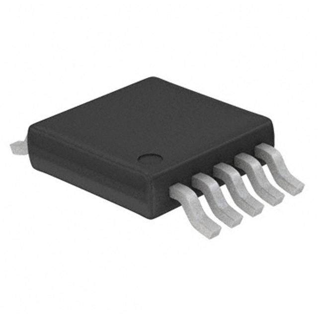
ICGOO在线商城 > LP5952TL-1.0/NOPB
- 型号: LP5952TL-1.0/NOPB
- 制造商: Texas Instruments
- 库位|库存: xxxx|xxxx
- 要求:
| 数量阶梯 | 香港交货 | 国内含税 |
| +xxxx | $xxxx | ¥xxxx |
查看当月历史价格
查看今年历史价格
LP5952TL-1.0/NOPB产品简介:
ICGOO电子元器件商城为您提供LP5952TL-1.0/NOPB由Texas Instruments设计生产,在icgoo商城现货销售,并且可以通过原厂、代理商等渠道进行代购。 提供LP5952TL-1.0/NOPB价格参考¥2.00-¥4.93以及Texas InstrumentsLP5952TL-1.0/NOPB封装/规格参数等产品信息。 你可以下载LP5952TL-1.0/NOPB参考资料、Datasheet数据手册功能说明书, 资料中有LP5952TL-1.0/NOPB详细功能的应用电路图电压和使用方法及教程。
| 参数 | 数值 |
| 产品目录 | 集成电路 (IC)半导体 |
| 描述 | IC REG LDO 1V 0.35A 5DSBGA低压差稳压器 350mA Dual Rail Linear Regulator 5-DSBGA -40 to 125 |
| 产品分类 | |
| 品牌 | Texas Instruments |
| 产品手册 | |
| 产品图片 |
|
| rohs | 符合RoHS无铅 / 符合限制有害物质指令(RoHS)规范要求 |
| 产品系列 | 电源管理 IC,低压差稳压器,Texas Instruments LP5952TL-1.0/NOPB- |
| 数据手册 | |
| 产品型号 | LP5952TL-1.0/NOPB |
| PCN组件/产地 | |
| 产品种类 | 低压差稳压器 |
| 供应商器件封装 | 5-DSBGA |
| 其它名称 | LP5952TL-1.0/NOPBTR |
| 包装 | 带卷 (TR) |
| 商标 | Texas Instruments |
| 安装类型 | 表面贴装 |
| 安装风格 | SMD/SMT |
| 封装 | Reel |
| 封装/外壳 | 5-WFBGA |
| 封装/箱体 | DSBGA-5 |
| 工作温度 | -40°C ~ 85°C |
| 工厂包装数量 | 250 |
| 最大工作温度 | + 125 C |
| 最大输入电压 | 5.5 V |
| 最小工作温度 | - 40 C |
| 最小输入电压 | 2.25 V |
| 标准包装 | 250 |
| 电压-跌落(典型值) | 0.088V @ 350mA |
| 电压-输入 | 最高 4.5 V |
| 电压-输出 | 1V |
| 电流-输出 | 350mA |
| 电流-限制(最小值) | - |
| 稳压器拓扑 | 正,固定式 |
| 稳压器数 | 1 |
| 系列 | LP5952 |
| 负载调节 | 60 mA |
| 输出电压 | 1.8 V |
| 输出电流 | 350 mA |


- 商务部:美国ITC正式对集成电路等产品启动337调查
- 曝三星4nm工艺存在良率问题 高通将骁龙8 Gen1或转产台积电
- 太阳诱电将投资9.5亿元在常州建新厂生产MLCC 预计2023年完工
- 英特尔发布欧洲新工厂建设计划 深化IDM 2.0 战略
- 台积电先进制程称霸业界 有大客户加持明年业绩稳了
- 达到5530亿美元!SIA预计今年全球半导体销售额将创下新高
- 英特尔拟将自动驾驶子公司Mobileye上市 估值或超500亿美元
- 三星加码芯片和SET,合并消费电子和移动部门,撤换高东真等 CEO
- 三星电子宣布重大人事变动 还合并消费电子和移动部门
- 海关总署:前11个月进口集成电路产品价值2.52万亿元 增长14.8%


-60DP-0.5V(86).jpg)
PDF Datasheet 数据手册内容提取
Product Sample & Technical Tools & Support & Folder Buy Documents Software Community LP5952 SNVS469F–OCTOBER2006–REVISEDDECEMBER2015 LP5952 350-mA Dual-Rail Linear Regulator 1 Features 3 Description • InputVoltageRange:0.7Vto4.5V The LP5952 is a dual-supply-rail linear regulator 1 optimizedforpoweringultralow-voltagecircuitsfroma • 2.5V≤ V ≤ 5.5V BATT singleLi-Ioncellor3-cellNiMH/NiCdbattery. • 0.5V≤ V ≤ 2V OUT In the typical post-regulation application V is • Ensured350-mAOutputCurrent BATT directlyconnectedtothebattery(range2.5Vto • ForILOAD=350mA: 5.5 V), and VIN is supplied by the output voltage of – V ≥ V +1.5Vor2.5V theDC-DCconverter(range0.7Vto4.5V). BATT OUT(NOM) (WhicheverisHigher) The device offers superior dropout and transient • ForI =150mA: features combined with very low quiescent currents. LOAD – V ≥ V +1.3Vor2.5V In shutdown mode (Enable (EN) pin pulled low) the BATT OUT(NOM) device turns off and reduces battery consumption to (WhicheverisHigher) 0.1 µA (typical). The LP5952 also features internal • ExcellentLoadTransientResponse:±15mV protection against overtemperature, overcurrent, and Typical undervoltageconditions. • ExcellentLineTransientResponse:±1mVTypical Depending upon application, only one or two tiny • 50-µATypicalQuiescentCurrentfromVBATT surface-mount external components are required; • 10-µATypicalQuiescentCurrentfromV performance is specified for a –40°C to +125°C IN junction temperature range. The device is available in • 0.1-µATypicalQuiescentCurrentinShutdown fixed output voltages from 0.5 V to 2 V. For • Noisevoltage=100µV Typical RMS availability, please contact your local Texas • OperatesfromaSingleLi-IonCellor3-Cell Instrumentssalesoffice. NiMH/NiCdBattery DeviceInformation(1) • Thermal-OverloadandShort-CircuitProtection PARTNUMBER PACKAGE BODYSIZE(NOM) 2 Applications DSBGA(5) 1.326mm×0.96mm LP5952 • MobilePhones USON(6) 2.00mm×2.00mm • Hand-HeldRadios (1) For all available packages, see the orderable addendum at theendofthedatasheet. • PersonalDigitalAssistants • Palm-TopPCs • PortableInstruments • Battery-PoweredDevices TypicalApplicationCircuit VBATT: 2.7 V to 5.5 V BATT OUT For example, 1.2 V C1 A3 Li-Ion 2.2 PF LP5952 or + For example, NiM3h-c/eNlilCd - Pre- 1.5 V IN A1 0 toL 3o5a0d mA regulator 1 PF EN GND C3 B2 1 An IMPORTANT NOTICE at the end of this data sheet addresses availability, warranty, changes, use in safety-critical applications, intellectualpropertymattersandotherimportantdisclaimers.PRODUCTIONDATA.
LP5952 SNVS469F–OCTOBER2006–REVISEDDECEMBER2015 www.ti.com Table of Contents 1 Features.................................................................. 1 7.1 Overview.................................................................10 2 Applications........................................................... 1 7.2 FunctionalBlockDiagram.......................................10 3 Description............................................................. 1 7.3 FeatureDescription.................................................10 7.4 DeviceFunctionalModes........................................11 4 RevisionHistory..................................................... 2 8 ApplicationandImplementation........................ 12 5 PinConfigurationandFunctions......................... 3 8.1 ApplicationInformation............................................12 6 Specifications......................................................... 4 8.2 TypicalApplication .................................................12 6.1 AbsoluteMaximumRatings......................................4 9 PowerSupplyRecommendations...................... 17 6.2 ESDRatings..............................................................4 10 Layout................................................................... 18 6.3 RecommendedOperatingConditions.......................4 6.4 ThermalInformation .................................................5 10.1 LayoutGuidelines.................................................18 6.5 ElectricalCharacteristics...........................................5 10.2 LayoutExamples...................................................18 6.6 ElectricalCharacteristics:QuiescentCurrents..........6 11 DeviceandDocumentationSupport................. 19 6.7 ElectricalCharacteristics:ShutdownCurrents..........6 11.1 DeviceSupport ....................................................19 6.8 ElectricalCharacteristics:EnableControl.................6 11.2 DocumentationSupport .......................................19 6.9 ElectricalCharacteristics:ThermalProtection..........7 11.3 CommunityResources..........................................19 6.10 ElectricalCharacteristics:Transient 11.4 Trademarks...........................................................19 Characteristics...........................................................7 11.5 ElectrostaticDischargeCaution............................19 6.11 InputandOutputCapacitors(Recommended).......7 11.6 Glossary................................................................19 6.12 TypicalCharacteristics............................................8 12 Mechanical,Packaging,andOrderable 7 DetailedDescription............................................ 10 Information........................................................... 19 4 Revision History NOTE:Pagenumbersforpreviousrevisionsmaydifferfrompagenumbersinthecurrentversion. ChangesfromRevisionE(May2013)toRevisionF Page • AddedDeviceInformationandPinConfigurationandFunctionssections,ESDRatingsandThermalInformation tables,FeatureDescription,DeviceFunctionalModes,ApplicationandImplementation,PowerSupply Recommendations,Layout,DeviceandDocumentationSupport,andMechanical,Packaging,andOrderable Informationsections;updatepinnamestoTInomenclature.................................................................................................. 1 • Deletedleadtempspec-itisinPOA ................................................................................................................................... 4 • Updatedthermalinformation ................................................................................................................................................. 5 • ChangedvaluesforthermalspecificationsinPowerDissipationsectionperupdatedthermalinformation .......................14 ChangesfromRevisionD(April2013)toRevisionE Page • ChangedlayoutofNationalDataSheettoTIformat........................................................................................................... 18 2 SubmitDocumentationFeedback Copyright©2006–2015,TexasInstrumentsIncorporated ProductFolderLinks:LP5952
LP5952 www.ti.com SNVS469F–OCTOBER2006–REVISEDDECEMBER2015 5 Pin Configuration and Functions YZRPackage 5-PinDSBGA TopView OUT EN A3 C3 A1 B2 C1 IN GND BATT NC-Nointernalconnection NKHPackage 6-PinUSON TopView BATT EN 1 6 GND NC 2 5 IN OUT 3 4 PinFunctions PIN TYPE DESCRIPTION NAME USON DSGBA BATT 1 C1 Input Biasinputvoltage;inputrange:2.5Vto5.5V Enablepinlogicinput:low=shutdown,high=active,normaloperation.This EN 6 C3 Input pinshouldnotbeleftfloating.TietoBATTifthisfunctionisnotused. GND 2 B2 Ground Ground IN 3 A1 Input Powerinputvoltage;inputrange:0.7Vto4.5V,V ≤V IN BATT NC 5 — — Donotmakeconnectionstothispin. OUT 4 A3 Output Regulatedoutputvoltage Copyright©2006–2015,TexasInstrumentsIncorporated SubmitDocumentationFeedback 3 ProductFolderLinks:LP5952
LP5952 SNVS469F–OCTOBER2006–REVISEDDECEMBER2015 www.ti.com 6 Specifications 6.1 Absolute Maximum Ratings overoperatingfree-airtemperaturerange(unlessotherwisenoted)(1)(2)(3) MIN MAX UNIT IN,BATTpins:VoltagetoGND,V ≤V –0.2 V IN BATT BATTpintoINpin 0.2 V ENpin,voltagetoGND –0.2 V Continuouspowerdissipation(4) Internallylimited JunctionTemperature(T ) 150 °C J-MAX Storagetemperature,T –65 150 °C stg (1) StressesbeyondthoselistedunderAbsoluteMaximumRatingsmaycausepermanentdamagetothedevice.Thesearestressratings only,whichdonotimplyfunctionaloperationofthedeviceattheseoranyotherconditionsbeyondthoseindicatedunderRecommended OperatingConditions.Exposuretoabsolute-maximum-ratedconditionsforextendedperiodsmayaffectdevicereliability. (2) AllvoltagesarewithrespecttothepotentialattheGNDpin. (3) IfMilitaryorAerospacespecifieddevicesarerequired,contactTexasInstrumentsSalesOfficeorDistributorsforavailabilityand specifications. (4) Internalthermalshutdowncircuitryprotectsthedevicefrompermanentdamage.ThermalshutdownengagesatT =165°C(typical)and J disengagesatT =145°C(typical). J 6.2 ESD Ratings VALUE UNIT Human-bodymodel(HBM),perANSI/ESDA/JEDECJS-001(1) ±2000 V Electrostaticdischarge V (ESD) Machinemodel ±200 (1) JEDECdocumentJEP155statesthat500-VHBMallowssafemanufacturingwithastandardESDcontrolprocess. 6.3 Recommended Operating Conditions overoperatingfree-airtemperaturerange(unlessotherwisenoted) MIN MAX UNIT Inputvoltage,V 0.7 4.5 V IN Inputvoltage,V 2.5 5.5 V BATT Inputvoltage,V 0 V V EN BATT Recommendedloadcurrent 0 350 mA Junctiontemperature,T –40 125 °C J Ambienttemperature,T (1) –40 85 °C A (1) Inapplicationswherehighpowerdissipationand/orpoorpackagethermalresistanceispresent,themaximumambienttemperaturemay havetobederated.Maximumambienttemperature(T )isdependentonthemaximumoperatingjunctiontemperature(T = A-MAX J-MAX-OP 125°C),themaximumpowerdissipationofthedeviceintheapplication(P ),andthejunction-toambientthermalresistanceofthe D-MAX part/packageintheapplication(R ),asgivenby:T =T –(R ×P ). θJA A-MAX J-MAX-OP θJA D-MAX 4 SubmitDocumentationFeedback Copyright©2006–2015,TexasInstrumentsIncorporated ProductFolderLinks:LP5952
LP5952 www.ti.com SNVS469F–OCTOBER2006–REVISEDDECEMBER2015 6.4 Thermal Information LP5952 THERMALMETRIC(1) YZR(DSBGA) NKH(USON) UNIT 5PINS 6PINS R Junction-to-ambientthermalresistance(2) 181.0 181.6 °C/W θJA R Junction-to-case(top)thermalresistance 0.9 93.1 °C/W θJC(top) R Junction-to-boardthermalresistance 110.3 116.7 °C/W θJB ψ Junction-to-topcharacterizationparameter 7.4 8.0 °C/W JT ψ Junction-to-boardcharacterizationparameter 110.3 116.7 °C/W JB (1) Formoreinformationabouttraditionalandnewthermalmetrics,seetheSemiconductorandICPackageThermalMetricsapplication report,SPRA953. (2) Junction-to-ambientthermalresistanceishighlyapplicationandboard-layoutdependent.Inapplicationswherehighmaximumpower dissipationexists,specialattentionmustbepaidtothermaldissipationissuesinboarddesign. 6.5 Electrical Characteristics Unlessotherwisenoted,typicalvaluesareforT =25°C,andminimumandmaximumlimitsapplyoverthefulloperating A temperaturerange:–40°C≤T ≤+125°C;specificationsapplytotheTypicalApplicationCircuitwithV =V +1V, J IN OUT(NOM) V =V +1.5Vor2.5V(whicheverishigher),I =1mA,C =1µF,C =2.2µF,V =V .(1)(2)(3) BATT OUT(NOM) OUT VIN OUT EN BATT PARAMETER TESTCONDITIONS MIN TYP MAX UNIT V =V +0.3V,T =25°C –1.5 1.5 IN OUT(NOM) A ΔV /V Outputvoltagetolerance OUT OUT V =V +0.3V 2 2 IN OUT(NOM) V =V +0.3Vto4.5V,V = 1 0.3 1 mV/V ΔV /ΔV IN OUT(NOM) BATT OUT IN 4.5V Lineregulationerror ΔV / V =V +1.5V(≥2.5V)to5.5 2.2 2.2 OUT BATT OUT(NOM) 0.5 ΔV V BATT DSBGA 30 I =1mAto350mA 15 30 µV/mA OUT package ΔV /ΔmA Loadregulationerror OUT USON 60 I =1mAto350mA 43 60 µV/mA OUT package Outputcurrent(short V =0V,V =V =V =V I OUT EN IN BATT OUT(NOM) 350 500 mA SC circuit) +1.5V I =350mA,V = DSBGA OUT IN 1.07 1.5 V V +0.3V package OUT(NOM) I =350mA USON OUT 1.08 1.5 V VDO_VBATT Outputvoltagedropout VIN=VOUT(NOM)+0.3V package (4) VBATT(5) IOUT=150mA DSBGA 0.96 1.3 V V =V +0.3V package IN OUT(NOM) I =150mA USON OUT 0.97 1.3 V V =V +0.3V package IN OUT(NOM) I =350mA OUT DSBGA V =V +1.5V 88 200 mV BATT OUT(NOM) package Outputvoltagedropout or2.5V V DO_VIN VIN IOUT=350mA USON V =V +1.5V 128 250 mV BATT OUT(NOM) package or2.5V E Outputnoise 10Hzto100kHz 100 µV N RMS (1) AllvoltagesarewithrespecttothepotentialattheGNDpin. (2) Minimumandmaximumlimitsareensuredbydesign,test,orstatisticalanalysis.Typicalnumbersarenotensured,butdorepresentthe mostlikelynorm.Unlessotherwisespecified,conditionsfortypicalspecificationsare:V =V +1V,V =V +1.5V IN OUT(NOM) BATT OUT(NOM) or2.5V,whicheverishigher,T =25°C. A (3) V isthestatedoutputvoltageoption OUT(NOM) (4) ThisspecificationdoesnotapplyifthebatteryvoltageV needstobedecreasedbelowtheminimumoperatinglimitof2.5Vduring BATT thistest. (5) Dropoutvoltageisdefinedastheinputtooutputvoltagedifferentialatwhichtheoutputvoltagefallsto100mVbelowthenominaloutput voltage. Copyright©2006–2015,TexasInstrumentsIncorporated SubmitDocumentationFeedback 5 ProductFolderLinks:LP5952
LP5952 SNVS469F–OCTOBER2006–REVISEDDECEMBER2015 www.ti.com Electrical Characteristics (continued) Unlessotherwisenoted,typicalvaluesareforT =25°C,andminimumandmaximumlimitsapplyoverthefulloperating A temperaturerange:–40°C≤T ≤+125°C;specificationsapplytotheTypicalApplicationCircuitwithV =V +1V, J IN OUT(NOM) V =V +1.5Vor2.5V(whicheverishigher),I =1mA,C =1µF,C =2.2µF,V =V .(1)(2)(3) BATT OUT(NOM) OUT VIN OUT EN BATT PARAMETER TESTCONDITIONS MIN TYP MAX UNIT SinemodulatedV ,ƒ=10Hz 70 BATT PowerSupplyRejection PSRR SinemodulatedV ,ƒ=100Hz 65 dB Ratio BATT SinemodulatedV ,ƒ=1kHz 45 BATT SinemodulatedV ,ƒ=10Hz 80 IN SinemodulatedV ,ƒ=100Hz 90 IN PowerSupplyRejection PSRR SinemodulatedV ,ƒ=1kHz 95 dB Ratio IN SinemodulatedV ,ƒ=10kHz 85 IN SinemodulatedV ,ƒ=100kHz 64 IN 6.6 Electrical Characteristics: Quiescent Currents Unlessotherwisenoted,typicalvaluesareforT =25°C,andminimumandmaximumlimitsapplyoverthefulloperating A temperaturerange:–40°C≤T ≤+125°C.(1)(2)(3) J PARAMETER TESTCONDITIONS MIN TYP MAX UNIT I CurrentintoV I =0mAto350mA 50 100 µA Q_VBATT BATT LOAD I CurrentintoV I =0 11 28 µA Q_VIN IN LOAD (1) AllvoltagesarewithrespecttothepotentialattheGNDpin. (2) Minimumandmaximumlimitsareensuredbydesign,test,orstatisticalanalysis.Typicalnumbersarenotensured,butdorepresentthe mostlikelynorm.Unlessotherwisespecified,conditionsfortypicalspecificationsare:V =V +1V,V =V +1.5V IN OUT(NOM) BATT OUT(NOM) or2.5V,whicheverishigher,T =25°C. A (3) V isthestatedoutputvoltageoption OUT(NOM) 6.7 Electrical Characteristics: Shutdown Currents Unlessotherwisenoted,typicalvaluesareforT =25°C,andminimumandmaximumlimitsapplyoverthefulloperating A temperaturerange:–40°C≤T ≤+125°C.(1)(2)(3) J PARAMETER TESTCONDITIONS MIN TYP MAX UNIT I CurrentintoV V =0V 0.1 1 µA Q_VBATT BATT EN I CurrentintoV V =0V 0.1 1 µA Q_VIN IN EN (1) AllvoltagesarewithrespecttothepotentialattheGNDpin. (2) Minimumandmaximumlimitsareensuredbydesign,test,orstatisticalanalysis.Typicalnumbersarenotensured,butdorepresentthe mostlikelynorm.Unlessotherwisespecified,conditionsfortypicalspecificationsare:V =V +1V,V =V +1.5V IN OUT(NOM) BATT OUT(NOM) or2.5V,whicheverishigher,T =25°C. A (3) V isthestatedoutputvoltageoption. OUT(NOM) 6.8 Electrical Characteristics: Enable Control Unlessotherwisenoted,typicalvaluesareforT =25°C,andminimumandmaximumlimitsapplyoverthefulloperating A temperaturerange:–40°C≤T ≤+125°C.(1)(2)(3) J PARAMETER TESTCONDITIONS MIN TYP MAX UNIT I MaximuminputcurrentatENinput 0.01 1 µA EN V Lowinputthreshold(shutdown) 0.4 V IL V Highinputthreshold(enable) 1 V IH (1) AllvoltagesarewithrespecttothepotentialattheGNDpin. (2) Minimumandmaximumlimitsareensuredbydesign,test,orstatisticalanalysis.Typicalnumbersarenotensured,butdorepresentthe mostlikelynorm.Unlessotherwisespecified,conditionsfortypicalspecificationsare:V =V +1V,V =V +1.5V IN OUT(NOM) BATT OUT(NOM) or2.5V,whicheverishigher,T =25°C. A (3) V isthestatedoutputvoltageoption. OUT(NOM) 6 SubmitDocumentationFeedback Copyright©2006–2015,TexasInstrumentsIncorporated ProductFolderLinks:LP5952
LP5952 www.ti.com SNVS469F–OCTOBER2006–REVISEDDECEMBER2015 6.9 Electrical Characteristics: Thermal Protection TypicalvaluesareforT =25°C.(1)(2)(3) A PARAMETER TESTCONDITIONS MIN TYP MAX UNIT T Thermal-shutdowntemperature 165 °C SHDN ΔT Thermal-shutdownhysteresis 20 °C SHDN (1) AllvoltagesarewithrespecttothepotentialattheGNDpin. (2) Minimumandmaximumlimitsareensuredbydesign,test,orstatisticalanalysis.Typicalnumbersarenotensured,butdorepresentthe mostlikelynorm.Unlessotherwisespecified,conditionsfortypicalspecificationsare:V =V +1V,V =V +1.5V IN OUT(NOM) BATT OUT(NOM) or2.5V,whicheverishigher,T =25°C. A (3) V isthestatedoutputvoltageoption. OUT(NOM) 6.10 Electrical Characteristics: Transient Characteristics Unlessotherwisenoted,typicalvaluesareforT =25°C,andminimumandmaximumlimitsapplyoverthefulloperating A temperaturerange:–40°C≤T ≤+125°C.(1)(2)(3) J PARAMETER TESTCONDITIONS MIN TYP MAX UNIT Dynamiclinetransient V =V +0.3Vto ΔV IN OUT(NOM) ±1 mV OUT responseV V +0.9V;tr,tf=10µs IN OUT(NOM) Dynamiclinetransient V =V +1.5Vto ΔV BATT OUT(NOM) ±15 mV OUT responseV V +2.1V;tr,tf=10µs BATT OUT(NOM) Pulsedload0...300mA, DSBGA ±15 mV Dynamicloadtransient di/dt=300mA/1µs package ΔV OUT response Pulsedload0...300mA,di/dt USONpackage –35/+15 mV =300mA/1µs T Start-uptime ENto0.95×V 70 150 µs STARTUP OUT (1) AllvoltagesarewithrespecttothepotentialattheGNDpin. (2) Minimumandmaximumlimitsareensuredbydesign,test,orstatisticalanalysis.Typicalnumbersarenotensured,butdorepresentthe mostlikelynorm.Unlessotherwisespecified,conditionsfortypicalspecificationsare:V =V +1V,V =V +1.5V IN OUT(NOM) BATT OUT(NOM) or2.5V,whicheverishigher,T =25°C. A (3) V isthestatedoutputvoltageoption. OUT(NOM) 6.11 Input and Output Capacitors (Recommended) AllvaluesareforT =25°C.(1)(2)(3) A PARAMETER TESTCONDITIONS MIN TYP MAX UNIT Capacitance(4) 1.5 2.2 10 µF C Outputcapacitance OUT ESR 3 300 mΩ Capacitance(4),notneededintypicalpost- 0.47 1 µF C InputcapacitanceatV regulationapplication(seeFigure18) VIN IN ESR 3 300 mΩ (1) AllvoltagesarewithrespecttothepotentialattheGNDpin. (2) Minimumandmaximumlimitsareensuredbydesign,test,orstatisticalanalysis.Typicalnumbersarenotensured,butdorepresentthe mostlikelynorm.Unlessotherwisespecified,conditionsfortypicalspecificationsare:V =V +1V,V =V +1.5V IN OUT(NOM) BATT OUT(NOM) or2.5V,whicheverishigher,T =25°C. A (3) V isthestatedoutputvoltageoption. OUT(NOM) (4) Thecapacitortoleranceshouldbe30%orbetterovertemperature.Thefulloperatingconditionsfortheapplicationshouldbeconsidered whenselectingasuitablecapacitortoensurethattheminimumvalueofcapacitanceisalwaysmet.Recommendedcapacitortypeis X7R.However,dependentonapplication,X5R,Y5V,andZ5Ucanalsobeused.Theshownminimumlimitrepresentsrealminimum capacitance,includingalltolerancesandmustbemaintainedovertemperatureandDCbiasvoltage(SeeDetailedDesignProcedurein ApplicationandImplementation.) Copyright©2006–2015,TexasInstrumentsIncorporated SubmitDocumentationFeedback 7 ProductFolderLinks:LP5952
LP5952 SNVS469F–OCTOBER2006–REVISEDDECEMBER2015 www.ti.com 6.12 Typical Characteristics Unlessotherwisespecified,T =25°C,C =1-µFceramic,C =2.2-µFceramic,V =V +1V,V =V + A IN OUT IN OUT(NOM) BATT OUT(NOM) 1.5V,ENpinistiedtoV (DSBGApackage). BATT 0.4 140 0.3 130 0.2 120 %) mV) ANGE ( 00..01 T V (IN 110100 H U C O UT -0.1 OP 90 O R V D -0.2 80 -0.3 70 -0.4 60 -40 -20 0 20 40 60 80 100 120 -40 -20 0 20 40 60 80 100 120 TEMPERATURE (°C) TEMPERATURE (°C) I =350mA LOAD Figure1.OutputVoltageChangevsTemperature Figure2.DropoutV vsTemperature IN 90 ILOAD = 0 V/ 80 VEN(500 mDIV) 70 TA = 125°C 0 A) 60 VOUT (500 mV/DIV) 0 (µQ_VBATT 5400 TA = 25°C A/ I TA = -40°C IIN100 mDIV)0 30 ( 20 TIME (10 Ps/DIV) 10 2.0 2.5 3.0 3.5 4.0 4.5 5.0 5.5 6.0 1.5-VOption VBATT (V) Figure3.InrushCurrentVIN Figure4.QuiescentCurrentIQ_VBATTvsVBATT 100 ILOAD = 0 90 GROUND CURRENT (Aµ) 6785400000 TTTAAA === 12-4250°5C°C°C GROUND CURRENT (A)µ 30 20 2.0 2.5 3.0 3.5 4.0 4.5 5.0 5.5 6.0 VBATT /VIN (V) LOAD CURRENT (mA) Figure5.GroundCurrentvsV /V Figure6.GroundCurrentvsLoadCurrent BATT IN 8 SubmitDocumentationFeedback Copyright©2006–2015,TexasInstrumentsIncorporated ProductFolderLinks:LP5952
LP5952 www.ti.com SNVS469F–OCTOBER2006–REVISEDDECEMBER2015 Typical Characteristics (continued) Unlessotherwisespecified,T =25°C,C =1-µFceramic,C =2.2-µFceramic,V =V +1V,V =V + A IN OUT IN OUT(NOM) BATT OUT(NOM) 1.5V,ENpinistiedtoV (DSBGApackage). BATT 0 0 CIN = 100nF -20 -20 )B )B IL = 300 mA d d ( N ( N O -40 O -40 IT IT C C EJER -60 IL = 50 mA EJER -60 E IL = 0 mA E LP LP PIR -80 PIR -80 IL = 0 mA 10 100 1k 10k 100k 1M 10 100 1k 10k 100k 1M FREQUENCY (Hz) FREQUENCY (Hz) 1.5-VOption 1.5-VOption Figure7.PowerSupplyRejectionRatioV Figure8.PowerSupplyRejectionRatioV IN BATT Copyright©2006–2015,TexasInstrumentsIncorporated SubmitDocumentationFeedback 9 ProductFolderLinks:LP5952
LP5952 SNVS469F–OCTOBER2006–REVISEDDECEMBER2015 www.ti.com 7 Detailed Description 7.1 Overview The LP5952 is a dual-supply-rail linear regulator optimized for powering ultralow-voltage circuits from a single Li- Ion cell or 3 cell NiMH/NiCd batteries. In a typical application, BATT is connected to the battery, and IN can be suppliedbytheoutputoffrontstageDC-DCConverter.INdoesnotexceedBATTatanytime. 7.2 Functional Block Diagram BATT IN VREF + - OUT Thermal, Enable and undervoltage, and EN start-up overcurrent management protection GND 7.3 Feature Description 7.3.1 Dual-RailSupply TheLP5952requirestwodifferentsupplyvoltages: • V ,thepowerinputvoltage,isregulatedtothefixedoutputvoltage. IN • V ,thebiasinputvoltage,suppliesinternalcircuitry. BATT It is important that V does not exceed V at any time. If the device is used in the typical post-regulation IN BATT application as shown in Figure 18, the sequencing of the two power supplies is not an issue because V BATT supplies both the DC-DC regulator and the LP5952 device. The output voltage of the DC-DC regulator takes some time to rise up and supply the input voltage of the device. In this application V always ramps up more IN slowlythanV . BATT IfV isshortedtoV ,thevoltagesatthetwosupplypinsrampupsimultaneouslycausingnoproblems. IN BATT However, in applications with two independent supplies connected to the LP5952, special care must be taken to ensurethatV isalways≤ V . IN BATT 7.3.2 No-LoadStability The LP5952 remains stable and in regulation with no external load. This is an important consideration in some circuits,forexample,CMOSRAMkeep-aliveapplications. 7.3.3 FastTurnon Fast turnon is ensured by an optimized architecture allowing a fast ramp of the output voltage to reach the target voltagewhiletheinrushcurrentiscontrolledlowat120mAtypical(foraC of2.2µF). OUT 10 SubmitDocumentationFeedback Copyright©2006–2015,TexasInstrumentsIncorporated ProductFolderLinks:LP5952
LP5952 www.ti.com SNVS469F–OCTOBER2006–REVISEDDECEMBER2015 Feature Description (continued) 7.3.4 Short-CircuitProtection The LP5952 is short-circuit protected and, in the event of a peak overcurrent condition, the output current throughtheNFETpassdeviceislimited. If the overcurrent condition exists for a longer time, the average power dissipation increases depending on the input-to-output voltage difference until the thermal shutdown circuitry turns the NFET off. Refer to Power DissipationandDeviceOperationforpowerdissipationcalculations. 7.3.5 Thermal-OverloadProtection Thermal-overload protection limits the total power dissipation in the LP5952. When the junction temperature exceeds T = 165°C typical, the shutdown logic is triggered, and the NFET is turned off, allowing the device to J cool down. After the junction temperature dropped by 20°C (temperature hysteresis) typical, the NFET is activatedagain.Thisresultsinapulsedoutputvoltageduringcontinuousthermal-overloadconditions. The thermal-overload protection is designed to protect the LP5952 in the event of a fault condition. For normal continuous operation, do not exceed the absolute maximum junction temperature rating of T = 150°C (see J AbsoluteMaximumRatings). 7.3.6 ReverseCurrentPath The internal NFET pass device in LP5952 has an inherent parasitic body diode. During normal operation, the inputvoltageishigherthantheoutputvoltage,andtheparasiticdiodeisreversebiased.However,iftheoutputis pulled above the input in an application, the current flows from the output to the input as the parasitic diode gets forwardbiased.Theoutputcanbepulledabovetheinputaslongasthecurrentintheparasiticdiodeislimitedto 50 mA. For currents above this limit an external Schottky diode must be connected from V to V (cathode on OUT IN V ,anodeonV ). IN OUT 7.4 Device Functional Modes 7.4.1 EnableOperation The LP5952 may be switched to an ON or OFF state by a logic input at the EN pin, V . A logic high at this pin EN turns the device on. When the enable pin is low, the regulator output is off, and the device typically consumes 0.1 µA. If the application does not require the enable switching feature, the EN pin must be tied to V to keep the BATT regulatoroutputpermanentlyon. Toensureproperoperation,thesignalsourceusedtodrivetheENinputmustbeabletoswingaboveandbelow the specified turnon and turnoff voltage thresholds shown in V and V in Electrical Characteristics: Enable IL IH Control. Copyright©2006–2015,TexasInstrumentsIncorporated SubmitDocumentationFeedback 11 ProductFolderLinks:LP5952
LP5952 SNVS469F–OCTOBER2006–REVISEDDECEMBER2015 www.ti.com 8 Application and Implementation NOTE Information in the following applications sections is not part of the TI component specification, and TI does not warrant its accuracy or completeness. TI’s customers are responsible for determining suitability of components for their purposes. Customers should validateandtesttheirdesignimplementationtoconfirmsystemfunctionality. 8.1 Application Information The LP5952 is designed to meet ultralow input-voltage application, by implementing V as power supply of BATT this device. The VBATT is connected to the battery (range 2.5 V to 5.5 V), the V range can be 0.7 V to 4.5 V. IN The device offers superior dropout and transient features combined with very low-quiescent currents. The LP5952 delivers this performance in standard packages DSBGA and USON with an operating junction temperature(T )of–40°Cto+125°C. J 8.2 Typical Application 8.2.1 Dual-RailLinearRegulator VBATT: 2.7 V to 5.5 V BATT OUT For example, 1.2 V C1 A3 Li-Ion 2.2 PF LP5952 or + For example, NiM3h-c/eNlilCd - Pre- 1.5 V IN A1 0 toL 3o5a0d mA regulator 1 PF EN GND C3 B2 Figure9. LP5952TypicalApplicationCircuit 8.2.1.1 DesignRequirements Fortypicaldual-raillinearregulatorparameters,seeTable1. Table1.DesignParameters DESIGNPARAMETER EXAMPLEVALUE Inputvoltagerange 0.7Vto4.5V V voltagerange 2.7Vto5.5V BATT Outputvoltage 1.5V Outputcurrent 350mA Outputcapacitorrange 2.2µF Input/outputcapacitorESRrange 3mΩto300mΩ 8.2.1.2 DetailedDesignProcedure 8.2.1.2.1 ExternalCapacitors As is common with most regulators, the LP5952 requires external capacitors to ensure stable operation. The LP5952 is specifically designed for portable applications requiring minimum board space and the smallest size components.Thesecapacitorsmustbecorrectlyselectedforgoodperformance. 8.2.1.2.2 InputCapacitor If the LP5952 is used as a stand-alone device, an input capacitor at V is required for stability. It is IN recommended that a 1-µF capacitor be connected between the LP5952 power voltage IN pin and ground. (This capacitancevaluemaybeincreasedwithoutlimit). 12 SubmitDocumentationFeedback Copyright©2006–2015,TexasInstrumentsIncorporated ProductFolderLinks:LP5952
LP5952 www.ti.com SNVS469F–OCTOBER2006–REVISEDDECEMBER2015 This capacitor must be located a distance of not more than 1 cm from the IN pin and returned to a clean analog ground.Anygoodqualityceramic,tantalum,orfilmcapacitormaybeusedattheinput. AcapacitoratV isnotrequiredifthedistancetothesupplydoesnotexceed5cm. BATT If the device is used in the typical application as post regulator after a DC-DC regulator, no input capacitors are required — the capacitors of the DC-DC regulator (C and C ) are sufficient if both components are mounted IN OUT close to each other and a proper GND plane is used. If the distance between the output capacitor of the DC-DC regulatorandtheINpinoftheLP5952islargerthan5cm,addinganinputcapacitoratV isrecommended. IN NOTE Important: Tantalum capacitors can suffer catastrophic failures due to surge current when connected to a low-impedance source of power (like a battery or a very large capacitor). If a tantalum capacitor is used at the input, it must be ensured by the manufacturertohaveasurgecurrentratingsufficientfortheapplication. The equivalent series resistance (ESR) of the input capacitor should be in the range of 3 mΩ to 300 mΩ. The tolerance and temperature coefficient must be considered when selecting the capacitor to ensure the capacitanceremains≥ 470nFovertheentireoperatingtemperaturerange. 8.2.1.2.3 OutputCapacitor The LP5952 is designed specifically to work with very small ceramic output capacitors. A ceramic capacitor (dielectrictypesX7R,Z5U,orY5V)inthe2.2-µFrange(upto10 µF)andwithanESRbetween3mΩ to300mΩ issuitableasC intheLP5952applicationcircuit. OUT This capacitor must be located a distance of not more than 1 cm from the OUT pin and returned to a clean analogground. It is also possible to use tantalum or film capacitors at the device output, V , but these are not as attractive for OUT reasonsofsizeandcost(seeCapacitorCharacteristics). 8.2.1.2.4 CapacitorCharacteristics The LP5952 is designed to work with ceramic capacitors on the output to take advantage of the benefits they offer. For capacitance values in the 1-µF to 4.7-µF range, ceramic capacitors are the smallest, least expensive and have the lowest ESR values, thus making them best for eliminating high-frequency noise. The ESR of a typical 1-µF ceramic capacitor is in the range of 3 mΩ to 40 mΩ, which easily meets the ESR requirement for stabilityfortheLP5952. For both input and output capacitors, careful interpretation of the capacitor specification is required to ensure correct device operation. The capacitor value can change greatly, depending on the operating conditions and capacitortype. In particular, the output capacitor selection must take account of all the capacitor parameters, to ensure that the specification is met within the application. The capacitance can vary with DC bias conditions as well as temperature and frequency of operation. Capacitor values show some decrease over time due to aging. The capacitor parameters are also dependant on the particular case size, with smaller sizes giving poorer performance figures in general. Figure 10 shows a typical graph comparing different capacitor case sizes in a capacitancevs.DCBiasplot.AsshownFigure10,increasingtheDC-biasconditioncanresultinthecapacitance value falling below the minimum value given in Input and Output Capacitors (Recommended) (0.47 µF or 1.5 µF in this case). The graph shows the capacitance out of specification for the 0402 case size capacitor at higher bias voltages. It is therefore recommended that the capacitor-manufacturer specifications for the nominal value capacitor are consulted for all conditions, as some capacitor sizes (such as 0402) may not be suitable in the actualapplication. Copyright©2006–2015,TexasInstrumentsIncorporated SubmitDocumentationFeedback 13 ProductFolderLinks:LP5952
LP5952 SNVS469F–OCTOBER2006–REVISEDDECEMBER2015 www.ti.com F)P100% 0603, 10V, X5R 1 m. o N 80% of % UE ( 60% L A P V 0402, 6.3V, X5R A 40% C 20% 0 1.0 2.0 3.0 4.0 5.0 DC BIAS (V) Figure10. TypicalVariationInCapacitancevsDCBias Capacitance of the ceramic capacitor can vary with temperature. The capacitor type X7R, which operates over a temperature range of –55°C to +125°C, only varies the capacitance to within ±15%. The capacitor type X5R has a similar tolerance over a reduced temperature range of –55°C to +85°C. Many large value ceramic capacitors, larger than 1 µF, are manufactured with Z5U or Y5V temperature characteristics. Their capacitance can drop by more than 50% as the temperature varies from 25°C to 85°C. Therefore, X7R is recommended over Z5U and Y5Vinapplicationswheretheambienttemperaturechangessignificantlyaboveorbelow25°C. Tantalum capacitors are less desirable than ceramic for use as output capacitors because they are more expensivewhencomparingequivalentcapacitanceandvoltageratingsinthe1-µFto4.7-µFrange. Another important consideration is that tantalum capacitors have higher ESR values than equivalent size ceramics. This means that while it may be possible to find a tantalum capacitor with an ESR value within the stable range, it would have to be larger in capacitance (which means bigger and more costly) than a ceramic capacitor with the same ESR value. The ESR of a typical tantalum increases about 2:1 as the temperature goes from25°Cdownto–40°C,sosomeguardbandmustbeallowed. 8.2.1.2.5 PowerDissipationandDeviceOperation The permissible power dissipation for any package is a measure of the capability of the device to pass heat from thepowersource,thejunctionsofthedevice,totheultimateheatsink,theambientenvironment.Thusthepower dissipation is dependent on the ambient temperature and the thermal resistance across the various interfaces betweenthedieandambientair. As stated in the Recommended Operating Conditions, the allowable power dissipation for the device in a given packagecanbecalculatedusingEquation1: P =(T –T )/R (1) D J(MAX) A θJA With an R = 181°C/W, the device in the 5-pin DSBGA package returns a value of 552 mW with a maximum RθJA junctiontemperatureof125°CatT of25°Cor221mWatT of85°C. A A TheactualpowerdissipationacrossthedevicecanbeestimatedbyEquation2: P =(V –V )×I (2) D IN OUT OUT 14 SubmitDocumentationFeedback Copyright©2006–2015,TexasInstrumentsIncorporated ProductFolderLinks:LP5952
LP5952 www.ti.com SNVS469F–OCTOBER2006–REVISEDDECEMBER2015 Thisestablishestherelationshipbetweenthepowerdissipationallowedduetothermalconsideration,thevoltage drop across the device, and the continuous current capability of the device. Equation 1 and Equation 2 must be usedtodeterminetheoptimumoperatingconditionsforthedeviceinanyapplication.Asanexample,tokeepfull load current capability of 350 mA for a 1.5-V output voltage option at a high ambient temperature of 85°C, V IN hastobekept≤ 2.1V(forDSBGApackage): V ≤P /I +V =221mW/350mA+1.5V=2.1V (3) IN D OUT OUT Figure11showstheoutputcurrentderatingduetotheseconsiderations: 350 DSBGA USON 300 250 A) m (AX 200 M D A O IL 150 100 50 0 0.5 1 1.5 2 2.5 3 3.5 4 VIN - VOUT (V) D001 T =85°C V =1.5V A OUT R =181°C/W R =181.6°C/W θJA(DSBGA) θJA(USON) Figure11. MaximumLoadCurrentvsV –V IN OUT The typical contribution of the bias input voltage supply V to the power dissipation can be neglected BATT (Equation4): P =V ×I =5.5V×50µA=0.275mWtypical (4) D_VBATT BATT QVBATT Copyright©2006–2015,TexasInstrumentsIncorporated SubmitDocumentationFeedback 15 ProductFolderLinks:LP5952
LP5952 SNVS469F–OCTOBER2006–REVISEDDECEMBER2015 www.ti.com 8.2.1.3 ApplicationCurves IL = 350 mA IL = 350 mA V) V) DI DI VEN0 mV/ VEN0 mV/ 0 0 5 0 5 0 ( ( V) V) DI DI OUTmV/ OUTmV/ V 0 V 0 0 0 0 0 2 5 ( ( TIME (10 µs/DIV) TIME (10 µs/DIV) 0.7-VOption 1.5-VOption Figure12.EnableStart-UpTime Figure13.EnableStart-UpTime mA) 350 mA) 350 T ( T ( N N E E R R R R U U C C D D A A O O L 0 L 0 V) V) TDI TDI VOUmV/ VOUmV/ ´ 0 ´ 0 1 1 ( ( TIME (50 µs/DIV) TIME (50 µs/DIV) 0.7-VOption 1.5-VOption Figure14.LoadTransientResponse Figure15.LoadTransientResponse VBATT = 3.1V IL = 350 mA V) IL = 350 mA VIN(500 mV/DI 23..51 VBATT00 mV/DIV) 33..06 5 ( V) OUTV/DI V) ´V (1 m VOUTmV/DI ´ 0 1 ( TIME (100 Ps/DIV) TIME (100 Ps/DIV) 1.5-VOption 1.5-VOption Figure16.LineTransientResponseV Figure17.LineTransientResponseV IN BATT 16 SubmitDocumentationFeedback Copyright©2006–2015,TexasInstrumentsIncorporated ProductFolderLinks:LP5952
LP5952 www.ti.com SNVS469F–OCTOBER2006–REVISEDDECEMBER2015 8.2.2 AdditionalApplicationCircuit BATT OUT 1.5 V C1 A3 VBATT VOUTDCDC LP5952 2.2 PF 3 V to 5.5 V VIN SW 1.8 V IN Load A1 B2 A1 0 to 350 mA L1: 2.2 PH 4.7 PF LM3671TL-1.8 10 PF GND A3 EN GND C3 B2 EN FB C1 C3 Figure18. TypicalApplicationCircuitWithDC-DCConverterasPre-RegulatorforV IN 9 Power Supply Recommendations This device is designed to operate from an input supply voltage range of 0.7 V to 4.5 V. The input supply should be well regulated and free of spurious noise. A minimum capacitor value of 1-μF is required to be within 1 cm of the IN pin. The V range is 2.5 V to 5.5 V and, in the typical application, V is connected to batteries. In BATT BATT anyapplication,V doesnotexceedV . IN BATT Copyright©2006–2015,TexasInstrumentsIncorporated SubmitDocumentationFeedback 17 ProductFolderLinks:LP5952
LP5952 SNVS469F–OCTOBER2006–REVISEDDECEMBER2015 www.ti.com 10 Layout 10.1 Layout Guidelines For best overall performance, place all circuit components on the same side of the circuit board and as near to the respective LDO pin connections as practical. Place ground return connections as close as possible to the input and output capacitor and to the LDO ground pin, connected by a wide, copper surface. The use of vias and longtracestocreateLDOcircuitconnectionisstronglydiscouragedandnegativelyaffectsystemperformance. 10.2 Layout Examples C OUT OUT EN OUT2 A3 C3 A1 B2 C1 IN GND BATT C C IN BATT Figure19. LP5952DSBGALayoutExample BATT 1 6 EN C BATT GND 2 5 NC CIN COUT IN 3 4 OUT Figure20. LP5952WSONLayoutExample 18 SubmitDocumentationFeedback Copyright©2006–2015,TexasInstrumentsIncorporated ProductFolderLinks:LP5952
LP5952 www.ti.com SNVS469F–OCTOBER2006–REVISEDDECEMBER2015 11 Device and Documentation Support 11.1 Device Support Foravailabilityofevaluationboards,refertotheproductfolderofLP5952atwww.ti.com. 11.2 Documentation Support 11.2.1 RelatedDocumentation Forinformationregardingevaluationboards,pleaserefertoAN-1531 LP5952EvaluationBoard(SNVA188). 11.3 Community Resources The following links connect to TI community resources. Linked contents are provided "AS IS" by the respective contributors. They do not constitute TI specifications and do not necessarily reflect TI's views; see TI's Terms of Use. TIE2E™OnlineCommunity TI'sEngineer-to-Engineer(E2E)Community.Createdtofostercollaboration amongengineers.Ate2e.ti.com,youcanaskquestions,shareknowledge,exploreideasandhelp solveproblemswithfellowengineers. DesignSupport TI'sDesignSupport QuicklyfindhelpfulE2Eforumsalongwithdesignsupporttoolsand contactinformationfortechnicalsupport. 11.4 Trademarks E2EisatrademarkofTexasInstruments. Allothertrademarksarethepropertyoftheirrespectiveowners. 11.5 Electrostatic Discharge Caution Thesedeviceshavelimitedbuilt-inESDprotection.Theleadsshouldbeshortedtogetherorthedeviceplacedinconductivefoam duringstorageorhandlingtopreventelectrostaticdamagetotheMOSgates. 11.6 Glossary SLYZ022—TIGlossary. Thisglossarylistsandexplainsterms,acronyms,anddefinitions. 12 Mechanical, Packaging, and Orderable Information The following pages include mechanical, packaging, and orderable information. This information is the most current data available for the designated devices. This data is subject to change without notice and revision of thisdocument.Forbrowser-basedversionsofthisdatasheet,refertotheleft-handnavigation. Copyright©2006–2015,TexasInstrumentsIncorporated SubmitDocumentationFeedback 19 ProductFolderLinks:LP5952
PACKAGE OPTION ADDENDUM www.ti.com 6-Feb-2020 PACKAGING INFORMATION Orderable Device Status Package Type Package Pins Package Eco Plan Lead/Ball Finish MSL Peak Temp Op Temp (°C) Device Marking Samples (1) Drawing Qty (2) (6) (3) (4/5) LP5952LC-1.2/NOPB ACTIVE USON NKH 6 1000 Green (RoHS NIPDAU Level-1-260C-UNLIM -40 to 125 L28 & no Sb/Br) LP5952LC-1.3/NOPB ACTIVE USON NKH 6 1000 Green (RoHS NIPDAU Level-1-260C-UNLIM -40 to 125 L43 & no Sb/Br) LP5952LC-1.5/NOPB ACTIVE USON NKH 6 1000 Green (RoHS NIPDAU Level-1-260C-UNLIM -40 to 125 L25 & no Sb/Br) LP5952LC-1.8/NOPB ACTIVE USON NKH 6 1000 Green (RoHS NIPDAU Level-1-260C-UNLIM -40 to 125 L29 & no Sb/Br) LP5952TL-1.0/NOPB ACTIVE DSBGA YZR 5 250 Green (RoHS SNAGCU Level-1-260C-UNLIM -40 to 125 L & no Sb/Br) LP5952TL-1.2/NOPB ACTIVE DSBGA YZR 5 250 Green (RoHS SNAGCU Level-1-260C-UNLIM -40 to 125 7 & no Sb/Br) LP5952TL-1.3/NOPB ACTIVE DSBGA YZR 5 250 Green (RoHS SNAGCU Level-1-260C-UNLIM -40 to 125 U & no Sb/Br) LP5952TL-1.5/NOPB ACTIVE DSBGA YZR 5 250 Green (RoHS SNAGCU Level-1-260C-UNLIM -40 to 125 T & no Sb/Br) LP5952TL-1.6/NOPB ACTIVE DSBGA YZR 5 250 Green (RoHS SNAGCU Level-1-260C-UNLIM -40 to 125 B & no Sb/Br) LP5952TL-1.8/NOPB ACTIVE DSBGA YZR 5 250 Green (RoHS SNAGCU Level-1-260C-UNLIM -40 to 125 8 & no Sb/Br) LP5952TLX-1.0/NOPB ACTIVE DSBGA YZR 5 3000 Green (RoHS SNAGCU Level-1-260C-UNLIM -40 to 125 L & no Sb/Br) LP5952TLX-1.2/NOPB ACTIVE DSBGA YZR 5 3000 Green (RoHS SNAGCU Level-1-260C-UNLIM -40 to 125 7 & no Sb/Br) LP5952TLX-1.5/NOPB ACTIVE DSBGA YZR 5 3000 Green (RoHS SNAGCU Level-1-260C-UNLIM -40 to 125 T & no Sb/Br) LP5952TLX-1.8/NOPB ACTIVE DSBGA YZR 5 3000 Green (RoHS SNAGCU Level-1-260C-UNLIM -40 to 125 8 & no Sb/Br) (1) The marketing status values are defined as follows: ACTIVE: Product device recommended for new designs. LIFEBUY: TI has announced that the device will be discontinued, and a lifetime-buy period is in effect. NRND: Not recommended for new designs. Device is in production to support existing customers, but TI does not recommend using this part in a new design. PREVIEW: Device has been announced but is not in production. Samples may or may not be available. OBSOLETE: TI has discontinued the production of the device. Addendum-Page 1
PACKAGE OPTION ADDENDUM www.ti.com 6-Feb-2020 (2) RoHS: TI defines "RoHS" to mean semiconductor products that are compliant with the current EU RoHS requirements for all 10 RoHS substances, including the requirement that RoHS substance do not exceed 0.1% by weight in homogeneous materials. Where designed to be soldered at high temperatures, "RoHS" products are suitable for use in specified lead-free processes. TI may reference these types of products as "Pb-Free". RoHS Exempt: TI defines "RoHS Exempt" to mean products that contain lead but are compliant with EU RoHS pursuant to a specific EU RoHS exemption. Green: TI defines "Green" to mean the content of Chlorine (Cl) and Bromine (Br) based flame retardants meet JS709B low halogen requirements of <=1000ppm threshold. Antimony trioxide based flame retardants must also meet the <=1000ppm threshold requirement. (3) MSL, Peak Temp. - The Moisture Sensitivity Level rating according to the JEDEC industry standard classifications, and peak solder temperature. (4) There may be additional marking, which relates to the logo, the lot trace code information, or the environmental category on the device. (5) Multiple Device Markings will be inside parentheses. Only one Device Marking contained in parentheses and separated by a "~" will appear on a device. If a line is indented then it is a continuation of the previous line and the two combined represent the entire Device Marking for that device. (6) Lead/Ball Finish - Orderable Devices may have multiple material finish options. Finish options are separated by a vertical ruled line. Lead/Ball Finish values may wrap to two lines if the finish value exceeds the maximum column width. Important Information and Disclaimer:The information provided on this page represents TI's knowledge and belief as of the date that it is provided. TI bases its knowledge and belief on information provided by third parties, and makes no representation or warranty as to the accuracy of such information. Efforts are underway to better integrate information from third parties. TI has taken and continues to take reasonable steps to provide representative and accurate information but may not have conducted destructive testing or chemical analysis on incoming materials and chemicals. TI and TI suppliers consider certain information to be proprietary, and thus CAS numbers and other limited information may not be available for release. In no event shall TI's liability arising out of such information exceed the total purchase price of the TI part(s) at issue in this document sold by TI to Customer on an annual basis. Addendum-Page 2
PACKAGE MATERIALS INFORMATION www.ti.com 24-Aug-2017 TAPE AND REEL INFORMATION *Alldimensionsarenominal Device Package Package Pins SPQ Reel Reel A0 B0 K0 P1 W Pin1 Type Drawing Diameter Width (mm) (mm) (mm) (mm) (mm) Quadrant (mm) W1(mm) LP5952LC-1.2/NOPB USON NKH 6 1000 178.0 12.4 2.2 2.2 1.0 8.0 12.0 Q1 LP5952LC-1.3/NOPB USON NKH 6 1000 178.0 12.4 2.2 2.2 1.0 8.0 12.0 Q1 LP5952LC-1.5/NOPB USON NKH 6 1000 178.0 12.4 2.2 2.2 1.0 8.0 12.0 Q1 LP5952LC-1.8/NOPB USON NKH 6 1000 178.0 12.4 2.2 2.2 1.0 8.0 12.0 Q1 LP5952TL-1.0/NOPB DSBGA YZR 5 250 178.0 8.4 1.04 1.4 0.76 4.0 8.0 Q1 LP5952TL-1.2/NOPB DSBGA YZR 5 250 178.0 8.4 1.04 1.4 0.76 4.0 8.0 Q1 LP5952TL-1.3/NOPB DSBGA YZR 5 250 178.0 8.4 1.04 1.4 0.76 4.0 8.0 Q1 LP5952TL-1.5/NOPB DSBGA YZR 5 250 178.0 8.4 1.04 1.4 0.76 4.0 8.0 Q1 LP5952TL-1.6/NOPB DSBGA YZR 5 250 178.0 8.4 1.04 1.4 0.76 4.0 8.0 Q1 LP5952TL-1.8/NOPB DSBGA YZR 5 250 178.0 8.4 1.04 1.4 0.76 4.0 8.0 Q1 LP5952TLX-1.0/NOPB DSBGA YZR 5 3000 178.0 8.4 1.04 1.4 0.76 4.0 8.0 Q1 LP5952TLX-1.2/NOPB DSBGA YZR 5 3000 178.0 8.4 1.04 1.4 0.76 4.0 8.0 Q1 LP5952TLX-1.5/NOPB DSBGA YZR 5 3000 178.0 8.4 1.04 1.4 0.76 4.0 8.0 Q1 LP5952TLX-1.8/NOPB DSBGA YZR 5 3000 178.0 8.4 1.04 1.4 0.76 4.0 8.0 Q1 PackMaterials-Page1
PACKAGE MATERIALS INFORMATION www.ti.com 24-Aug-2017 *Alldimensionsarenominal Device PackageType PackageDrawing Pins SPQ Length(mm) Width(mm) Height(mm) LP5952LC-1.2/NOPB USON NKH 6 1000 210.0 185.0 35.0 LP5952LC-1.3/NOPB USON NKH 6 1000 210.0 185.0 35.0 LP5952LC-1.5/NOPB USON NKH 6 1000 210.0 185.0 35.0 LP5952LC-1.8/NOPB USON NKH 6 1000 210.0 185.0 35.0 LP5952TL-1.0/NOPB DSBGA YZR 5 250 210.0 185.0 35.0 LP5952TL-1.2/NOPB DSBGA YZR 5 250 210.0 185.0 35.0 LP5952TL-1.3/NOPB DSBGA YZR 5 250 210.0 185.0 35.0 LP5952TL-1.5/NOPB DSBGA YZR 5 250 210.0 185.0 35.0 LP5952TL-1.6/NOPB DSBGA YZR 5 250 210.0 185.0 35.0 LP5952TL-1.8/NOPB DSBGA YZR 5 250 210.0 185.0 35.0 LP5952TLX-1.0/NOPB DSBGA YZR 5 3000 210.0 185.0 35.0 LP5952TLX-1.2/NOPB DSBGA YZR 5 3000 210.0 185.0 35.0 LP5952TLX-1.5/NOPB DSBGA YZR 5 3000 210.0 185.0 35.0 LP5952TLX-1.8/NOPB DSBGA YZR 5 3000 210.0 185.0 35.0 PackMaterials-Page2
MECHANICAL DATA YZR0005xxx D 0.600±0.075 E TLA05XXX (Rev C) D: Max = 1.356 mm, Min =1 .296 mm E: Max = 0.99 mm, Min = 0.93 mm 4215043/A 12/12 NOTES: A.Alllineardimensionsareinmillimeters.DimensioningandtolerancingperASMEY14.5M-1994. B.Thisdrawingissubjecttochangewithoutnotice. www.ti.com
MECHANICAL DATA NKH0006B LCA06B (Rev A) www.ti.com
IMPORTANTNOTICEANDDISCLAIMER TI PROVIDES TECHNICAL AND RELIABILITY DATA (INCLUDING DATASHEETS), DESIGN RESOURCES (INCLUDING REFERENCE DESIGNS), APPLICATION OR OTHER DESIGN ADVICE, WEB TOOLS, SAFETY INFORMATION, AND OTHER RESOURCES “AS IS” AND WITH ALL FAULTS, AND DISCLAIMS ALL WARRANTIES, EXPRESS AND IMPLIED, INCLUDING WITHOUT LIMITATION ANY IMPLIED WARRANTIES OF MERCHANTABILITY, FITNESS FOR A PARTICULAR PURPOSE OR NON-INFRINGEMENT OF THIRD PARTY INTELLECTUAL PROPERTY RIGHTS. These resources are intended for skilled developers designing with TI products. You are solely responsible for (1) selecting the appropriate TI products for your application, (2) designing, validating and testing your application, and (3) ensuring your application meets applicable standards, and any other safety, security, or other requirements. These resources are subject to change without notice. TI grants you permission to use these resources only for development of an application that uses the TI products described in the resource. Other reproduction and display of these resources is prohibited. No license is granted to any other TI intellectual property right or to any third party intellectual property right. TI disclaims responsibility for, and you will fully indemnify TI and its representatives against, any claims, damages, costs, losses, and liabilities arising out of your use of these resources. TI’s products are provided subject to TI’s Terms of Sale (www.ti.com/legal/termsofsale.html) or other applicable terms available either on ti.com or provided in conjunction with such TI products. TI’s provision of these resources does not expand or otherwise alter TI’s applicable warranties or warranty disclaimers for TI products. Mailing Address: Texas Instruments, Post Office Box 655303, Dallas, Texas 75265 Copyright © 2020, Texas Instruments Incorporated

 Datasheet下载

