ICGOO在线商城 > 集成电路(IC) > PMIC - 稳压器 - 线性 > LP3996SD-1525/NOPB

 Datasheet下载
- 型号: LP3996SD-1525/NOPB
- 制造商: Texas Instruments
- 库位|库存: xxxx|xxxx
- 要求:
| 数量阶梯 | 香港交货 | 国内含税 |
| +xxxx | $xxxx | ¥xxxx |
查看当月历史价格
查看今年历史价格
LP3996SD-1525/NOPB产品简介:
ICGOO电子元器件商城为您提供LP3996SD-1525/NOPB由Texas Instruments设计生产,在icgoo商城现货销售,并且可以通过原厂、代理商等渠道进行代购。 LP3996SD-1525/NOPB价格参考。Texas InstrumentsLP3996SD-1525/NOPB封装/规格:PMIC - 稳压器 - 线性, Linear Voltage Regulator IC Positive Fixed 2 Output 1.5V, 2.5V 150mA, 300mA 10-WSON (3x3)。您可以下载LP3996SD-1525/NOPB参考资料、Datasheet数据手册功能说明书,资料中有LP3996SD-1525/NOPB 详细功能的应用电路图电压和使用方法及教程。
LP3996SD-1525/NOPB 是由德州仪器(Texas Instruments)生产的一款线性稳压器,属于 PMIC(电源管理集成电路)系列。其主要应用场景包括以下方面:

 1. 便携式电子设备
   - 电池供电设备:LP3996SD-1525/NOPB 具有低功耗和高效率的特点,非常适合用于电池供电的便携式设备,如智能手机、平板电脑、可穿戴设备(智能手表、健康监测器)等。
   - 手持设备:例如 GPS 导航仪、手持扫描仪、游戏机等需要稳定电压输出的设备。

 2. 通信设备
   - 无线模块:适用于蓝牙模块、Wi-Fi 模块、Zigbee 模块等低功耗无线通信设备。
   - 路由器/网关:为小型家庭或工业用的路由器、物联网网关提供稳定的电源支持。

 3. 消费类电子产品
   - 音频设备:如便携式音箱、耳机放大器等需要低噪声电源供应的音频应用。
   - 智能家居设备:包括智能灯泡、智能插座、安防摄像头等,这些设备通常对电源的稳定性要求较高。

 4. 工业控制与自动化
   - 传感器系统:为温度传感器、压力传感器、湿度传感器等提供精确的电源支持。
   - 数据采集设备:如数据记录仪、信号调理器等需要低功耗和高精度电源的应用。

 5. 医疗设备
   - 便携式医疗仪器:如脉搏血氧仪、血糖仪、便携式超声设备等,这些设备需要低噪声、高可靠性的电源解决方案。
   - 健康监测设备:例如智能手环、心率监测器等。

 6. 汽车电子
   - 车载信息娱乐系统:为车内的音响系统、导航系统等提供稳定的电源。
   - 辅助驾驶系统:如倒车雷达、行车记录仪等需要高效电源管理的设备。

 特点总结:
- 低功耗:适合对功耗敏感的应用场景。
- 低噪声:特别适合对电源质量要求较高的音频和射频应用。
- 小封装:节省空间,适合紧凑型设计。
- 高可靠性:能够在各种环境下稳定工作,满足工业和医疗领域的需求。

综上所述,LP3996SD-1525/NOPB 广泛应用于需要高效、低功耗、低噪声电源解决方案的各种电子设备中,尤其在便携式设备、通信设备和医疗设备领域表现突出。
| 参数 | 数值 |
| 产品目录 | 集成电路 (IC)半导体 |
| 描述 | IC REG LDO 1.5V/2.5V 10WSON低压差稳压器 Dual Linear Regulator with 300mA and 150mA Outputs and Power-On-Reset 10-WSON -40 to 85 |
| DevelopmentKit | LP3996SD-3033EV |
| 产品分类 | |
| 品牌 | Texas Instruments |
| 产品手册 | |
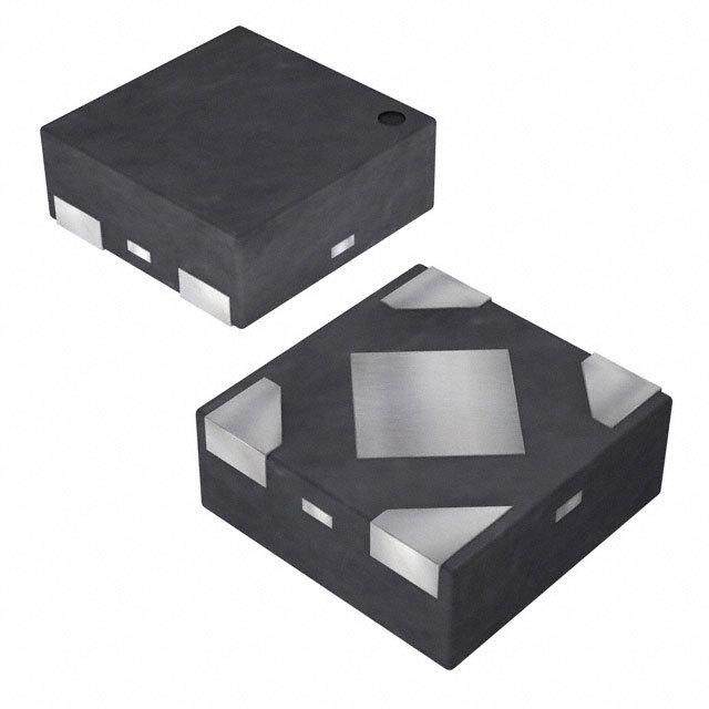
| 产品图片 |
|
| rohs | 符合RoHS无铅 / 符合限制有害物质指令(RoHS)规范要求 |
| 产品系列 | 电源管理 IC,低压差稳压器,Texas Instruments LP3996SD-1525/NOPB- |
| 数据手册 | |
| 产品型号 | LP3996SD-1525/NOPB |
| PSRR/纹波抑制—典型值 | 70 dB |
| 产品 | Dual Linear Regulators |
| 产品种类 | 低压差稳压器 |
| 供应商器件封装 | 10-WSON (3x3) |
| 其它名称 | LP3996SD-1525/NOPBTR |
| 包装 | 带卷 (TR) |
| 商标 | Texas Instruments |
| 回动电压—最大值 | 210 mV at 300 mA |
| 安装类型 | 表面贴装 |
| 安装风格 | SMD/SMT |
| 封装 | Reel |
| 封装/外壳 | 10-WFDFN 裸露焊盘 |
| 封装/箱体 | WSON-10 |
| 工作温度 | -40°C ~ 85°C |
| 工厂包装数量 | 1000 |
| 最大工作温度 | + 85 C |
| 最大输入电压 | 6 V |
| 最小工作温度 | - 40 C |
| 最小输入电压 | 2 V |
| 标准包装 | 1,000 |
| 电压-跌落(典型值) | -,0.21V @ 300mA |
| 电压-输入 | 2 V ~ 6 V |
| 电压-输出 | 1.5V,2.5V |
| 电流-输出 | 150mA,300mA |
| 电流-限制(最小值) | - |
| 稳压器拓扑 | 正,固定式 |
| 稳压器数 | 2 |
| 类型 | Dual Low Dropout Regulator |
| 系列 | LP3996 |
| 线路调整率 | 0.03 % |
| 负载调节 | 85 uV/mA, 26 uV/mA |
| 输出电压 | 1.5 V, 2.5 V |
| 输出电压容差 | +/- 4 % |
| 输出电流 | 150 mA |
| 输出端数量 | 2 Output |
| 输出类型 | Adjustable |
| 配用 | /product-detail/zh/LP3996SD-3333EV/LP3996SD-3333EV-ND/1640888/product-detail/zh/LP3996SD-3033EV/LP3996SD-3033EV-ND/1640887/product-detail/zh/LP3996SD-3030EV/LP3996SD-3030EV-ND/1640886/product-detail/zh/LP3996SD-2828EV/LP3996SD-2828EV-ND/1640885 |


PDF Datasheet 数据手册内容提取
LP3996 www.ti.com SNVS360D–NOVEMBER2006–REVISEDOCTOBER2013 LP3996 Dual Linear Regulator with 300 mA and 150 mA Outputs and Power-On-Reset CheckforSamples:LP3996 FEATURES APPLICATIONS 1 • 2LDOOutputswithIndependentEnable • CellularHandsets 2 • 1.5%AccuracyatRoomTemperature,3%Over • PDAs Temperature • WirelessNetworkAdaptors • Power-On-ResetFunctionwithAdjustable Delay DESCRIPTION • ThermalShutdownProtection The LP3996 is a dual low dropout regulator with power-on-reset circuit. The first regulator can source • StablewithCeramicCapacitors 150 mA, while the second is capable of sourcing 300 mAandhasapower-on-resetfunctionincluded. KEY SPECIFICATIONS The LP3996 provides 1.5% accuracy requiring an • InputVoltageRange2.0Vto6.0V ultra low quiescent current of 35 µA. Separate enable • LowDropoutVoltage210mVat300mA pins allow each output of the LP3996 to be shut • Ultra-LowI (Enabled)35µA down,drawingvirtuallyzerocurrent. Q • VirtuallyZeroI (Disabled)<10nA The LP3996 is designed to be stable with small Q • PackageAvailableinLead-FreeOption footprint ceramic capacitors down to 1 µF. An external capacitor may be used to set the POR delay 10-pin3mmx3mm timeasrequired. The LP3996 is available in fixed output voltages and comesina10-pin,3mmx3mmpackage. Typical Application Circuit 470 k: LP3996 VIN VIN VOUT1 VOUT1 EN1 EN1 VOUT2 VOUT2 EN2 EN2 POR POR CBYP SET 1 PF 10 nF 1 PF 1 PF GND Sets delay for POR 1 Pleasebeawarethatanimportantnoticeconcerningavailability,standardwarranty,anduseincriticalapplicationsof TexasInstrumentssemiconductorproductsanddisclaimerstheretoappearsattheendofthisdatasheet. Alltrademarksarethepropertyoftheirrespectiveowners. 2 PRODUCTIONDATAinformationiscurrentasofpublicationdate. Copyright©2006–2013,TexasInstrumentsIncorporated Products conform to specifications per the terms of the Texas Instruments standard warranty. Production processing does not necessarilyincludetestingofallparameters.
LP3996 SNVS360D–NOVEMBER2006–REVISEDOCTOBER2013 www.ti.com Functional Block Diagram VIN LDO1 VOUT1 EN1 LDO2 VOUT2 EN2 POR POR CBYP 1 PA VREF +- GND SET PinFunctions PinNo Symbol NameandFunction 1 V VoltageSupplyInput.Connecta1µFcapacitorbetweenthispinandGND. IN 2 EN1 EnableInputtoRegulator1.Activehighinput. High=On.Low=OFF. 3 EN2 EnableInputtoRegulator2.Activehighinput. High=On.Low=OFF. 4 C InternalVoltageReferenceBypass.Connecta10nFcapacitorfromthispintoGNDtoreduceoutput BYP noiseandimprovelinetransientandPSRR. Thispinmaybeleftopen. 5 SET SetDelayInput.ConnectacapacitorbetweenthispinandGNDtosetthePORdelaytime.Ifleftopen, therewillbenodelay. 6 GND CommonGroundpin.Connectexternallytoexposedpad. 7 N/C NoConnection.Donotconnecttoanyotherpin. 8 POR Power-OnResetOutput.Opendrainoutput.Activelowindicatesunder-voltageoutputonRegulator2. Apull-upresistorisrequiredforcorrectoperation. 9 V OutputofRegulator2.300mAmaximumcurrentoutput.Connecta1µFcapacitorbetweenthispin OUT2 andGND. 10 V OutputofRegulator1.150mAmaximumcurrentoutput.Connecta1µFcapacitorbetweenthispin OUT1 andGND. Pad GND CommonGround.ConnecttoPin6. 2 SubmitDocumentationFeedback Copyright©2006–2013,TexasInstrumentsIncorporated ProductFolderLinks:LP3996
LP3996 www.ti.com SNVS360D–NOVEMBER2006–REVISEDOCTOBER2013 Connection Diagram VOUT1 VOUT2 POR N/C GND 10 9 8 7 6 GND 1 2 3 4 5 VIN EN1 EN2 CBYP SET Top View Figure1. WSON-10Package SeePackageNumberDSC0010A Table1.AdditionalDeviceInformation (1) VOUT1/VOUT2(V) ORDERNUMBER 0.8/3.3 LP3996SD/X-0833/NOPB 1.0/1.8 LP3996SD/X-1018/NOPB 1.5/2.5 LP3996SD/X-1525/NOPB 1.8/3.3 LP3996SD/X-1833/NOPB 2.5/3.3 LP3996SD/X-2533/NOPB 2.8/2.8 LP3996SD/X-2828/NOPB 3.0/3.0 LP3996SD/X-3030/NOPB 3.0/3.3 LP3996SD/X-3033/NOPB 3.3/0.8 LP3996SD/X-3308/NOPB 3.3/3.3 LP3996SD/X-3333/NOPB (1) Forthemostcurrentpackageandorderinginformation,seethePackageOptionAddendumattheendofthisdocument,orseetheTI websiteatwww.ti.com. Thesedeviceshavelimitedbuilt-inESDprotection.Theleadsshouldbeshortedtogetherorthedeviceplacedinconductivefoam duringstorageorhandlingtopreventelectrostaticdamagetotheMOSgates. Copyright©2006–2013,TexasInstrumentsIncorporated SubmitDocumentationFeedback 3 ProductFolderLinks:LP3996
LP3996 SNVS360D–NOVEMBER2006–REVISEDOCTOBER2013 www.ti.com ABSOLUTE MAXIMUM RATINGS(1)(2) InputVoltagetoGND –0.3Vto6.5V V ,V EN1andEN2VoltagetoGND –0.3Vto(V +0.3V)with6.5V OUT1 OUT2 IN (max) PORtoGND –0.3Vto6.5V JunctionTemperature(T ) 150°C J-MAX Lead/PadTemp(3) 235°C StorageTemperature –65°Cto150°C ContinuousPowerDissipationInternallyLimited(4) HumanBodyModel 2.0kV ESDRating(5) MachineModel 200V (1) AllVoltagesarewithrespecttothepotentialattheGNDpin. (2) AbsoluteMaximumRatingsarelimitsbeyondwhichdamagecanoccur.RecommendedOperatingConditionsareconditionsunder whichoperationofthedeviceisensured.RecommendedOperatingConditionsdonotimplyensuredperformancelimits.Forensured performancelimitsandassociatedtestconditions,seetheElectricalCharacteristicstables. (3) Fordetailedsolderingspecificationsandinformation,pleaserefertoTexasInstrumentsApplicationNoteAN-1187,LeadlessLeadframe Package. (4) Internalthermalshutdowncircuitryprotectsthedevicefrompermanentdamage. (5) Thehumanbodymodelis100pFdischargedthrougha1.5kΩresistorintoeachpin.Themachinemodelisa200pFcapacitor dischargeddirectlyintoeachpin. RECOMMENDED OPERATING CONDITIONS(1)(2) InputVoltage 2.0Vto6.0V EN1,EN2,PORVoltage 0to(V +0.3V)to6.0V(max) IN JunctionTemperature –40°Cto125°C AmbientTemperatureT Range(3) –40°Cto85°C A (1) AbsoluteMaximumRatingsarelimitsbeyondwhichdamagecanoccur.RecommendedOperatingConditionsareconditionsunder whichoperationofthedeviceisensured.RecommendedOperatingConditionsdonotimplyensuredperformancelimits.Forensured performancelimitsandassociatedtestconditions,seetheElectricalCharacteristicstables. (2) AllVoltagesarewithrespecttothepotentialattheGNDpin. (3) Themaximumambienttemperature(T )isdependantonthemaximumoperatingjunctiontemperature(T =125°C),the A(max) J(max-op) maximumpowerdissipationofthedeviceintheapplication(P ),andthejunctiontoambientthermalresistanceofthepart/package D(max) intheapplication(θ ),asgivenbythefollowingequation:T =T -(θ ×P ). JA A(max) J(max-op) JA D(max) THERMAL PROPERTIES(1) Junction-To-AmbientThermalResistance(2) θ WSON-10Package 55°C/W JA (1) AbsoluteMaximumRatingsarelimitsbeyondwhichdamagecanoccur.RecommendedOperatingConditionsareconditionsunder whichoperationofthedeviceisensured.RecommendedOperatingConditionsdonotimplyensuredperformancelimits.Forensured performancelimitsandassociatedtestconditions,seetheElectricalCharacteristicstables. (2) Junction-to-ambientthermalresistanceisdependantontheapplicationandboardlayout.Inapplicationswherehighmaximumpower dissipationispossible;specialcaremustbepaidtothermaldissipationissuesinboarddesign. 4 SubmitDocumentationFeedback Copyright©2006–2013,TexasInstrumentsIncorporated ProductFolderLinks:LP3996
LP3996 www.ti.com SNVS360D–NOVEMBER2006–REVISEDOCTOBER2013 ELECTRICAL CHARACTERISTICS(1)(2) Unlessotherwisenoted,V =950mV,V =V +1.0V,or2.0V,whicheverishigher,whereV isthehigherofV and EN IN OUT OUT OUT1 V .C =1µF,I =1mA,C =C =1.0µF. OUT2 IN OUT OUT1 OUT2 TypicalvaluesandlimitsappearinginnormaltypeapplyforT =25°C.Limitsappearinginboldfacetypeapplyoverthefull A junctiontemperaturerangeforoperation,−40to+125°C. LIMIT SYMBOL PARAMETER CONDITIONS TYP UNITS MIN MAX V InputVoltage See(3) 2 6 V IN ΔV OutputVoltageTolerance I =1mA 1.5V<V ≤3.3V –2.5 +2.5 OUT OUT OUT –3.75 +3.75 % V ≤1.5V –2.75 +2.75 OUT –4 +4 LineRegulationError V =(V +1.0V)to6.0V 0.03 0.3 %/V IN OUT(NOM) LoadRegulationError I =1mAto150mA OUT 85 155 (LDO1) µV/mA I =1mAto300mA OUT 26 85 (LDO2) V DropoutVoltage(4) I =1mAto150mA DO OUT 110 220 (LDO1) mV I =1mAto300mA OUT 210 550 (LDO2) I QuiescentCurrent LDO1ON,LDO2ON Q 35 100 I =I =0mA OUT1 OUT2 LDO1ON,LDO2OFF 45 110 I =150mA OUT1 µA LDO1OFF,LDO2ON 45 110 I =300mA OUT2 LDO1ON,LDO2ON 70 170 I =150mA,I =300mA OUT1 OUT2 V =V =0.4V 0.5 10 nA EN1 EN2 (1) AllVoltagesarewithrespecttothepotentialattheGNDpin. (2) MinandMaxlimitsarespecifiedbydesign,testorstatisticalanalysis.Typicalnumbersarenotensured,butdorepresentthemostlikely norm. (3) V =V +0.5V,or2.0V,whicheverishigher. IN(MIN) OUT(NOM) (4) Dropoutvoltageisvoltagedifferencebetweeninputandoutputatwhichtheoutputvoltagedropsto100mVbelowitsnominalvalue. Thisparameteronlyforoutputvoltagesabove2.0V Copyright©2006–2013,TexasInstrumentsIncorporated SubmitDocumentationFeedback 5 ProductFolderLinks:LP3996
LP3996 SNVS360D–NOVEMBER2006–REVISEDOCTOBER2013 www.ti.com ELECTRICAL CHARACTERISTICS(1)(2) (continued) Unlessotherwisenoted,V =950mV,V =V +1.0V,or2.0V,whicheverishigher,whereV isthehigherofV and EN IN OUT OUT OUT1 V .C =1µF,I =1mA,C =C =1.0µF. OUT2 IN OUT OUT1 OUT2 TypicalvaluesandlimitsappearinginnormaltypeapplyforT =25°C.Limitsappearinginboldfacetypeapplyoverthefull A junctiontemperaturerangeforoperation,−40to+125°C. LIMIT SYMBOL PARAMETER CONDITIONS TYP UNITS MIN MAX I ShortCircuitCurrentLimit LDO1 420 750 SC mA LDO2 550 840 I MaximumOutputCurrent LDO1 150 OUT mA LDO2 300 PSRR PowerSupplyRejectionRatio(5) f=1kHz,I = LDO1 58 OUT 1mAto150mA C =10nF LDO2 70 BYP f=20kHz,I LDO1 45 dB OUT =1mAto150 mA LDO2 60 C =10nF BYP e OutputnoiseVoltage(5) BW=10Hzto V =0.8V 36 n OUT 100kHz µV C =10nF VOUT=3.3V 75 RMS BYP T ThermalShutdown Temperature 160 SHUTDOWN °C Hysteresis 20 EnableControlCharacteristics I InputCurrentatV orV V =0.0V 0.005 0.1 EN EN1 EN2 EN µA V =6V 2 5 EN V LowInputThresholdatV or IL EN1 0.4 V V EN2 V HighInputThresholdatV or IH EN1 0.95 V V EN2 POROutputCharacteristics V LowThreshold%0fV FlagON 88 TH OUT2(NOM) % HighThreshold%0fV FlagOFF 96 OUT2(NOM) I LeakageCurrent FlagOFF,V =6.5V 30 nA POR POR V FlagOutputLowVoltage I =250µA 20 mV OL SINK TimingCharacteristics T TurnOnTime(5) To95%Level ON 300 µs C =10nF BYP Transient LineTransientResponse T =T =10µs Response |δV |(5) δVrise =1fValCl =10nF 20 OUT IN BYP LoadTransientResponse T =T =1 LDO1 rise fall |δV |(5) µs I =1mAto150 175 mV OUT OUT mA (pk-pk) LDO2 I =1mAto300 150 OUT mA SETInputCharacteristics I SETPinCurrentSource V =0V 1.3 µA SET SET V SETPinThresholdVoltage POR=High 1.25 V TH(SET) (5) Thiselectricalspecificationisspecifiedbydesign. 6 SubmitDocumentationFeedback Copyright©2006–2013,TexasInstrumentsIncorporated ProductFolderLinks:LP3996
LP3996 www.ti.com SNVS360D–NOVEMBER2006–REVISEDOCTOBER2013 OUTPUT CAPACITOR, RECOMMENDED SPECIFICATIONS LIMIT SYMBOL PARAMETER CONDITIONS NOM UNITS MIN MAX C OutputCapacitance Capacitance(1) 1.0 0.7 µF OUT ESR 5 500 mΩ (1) TheCapacitortoleranceshouldbe30%orbetterovertemperature.Thefulloperatingconditionsfortheapplicationshouldbe consideredwhenselectingasuitablecapacitortoensurethattheminimumvalueofcapacitanceisalwaysmet.Recommended capacitorisX7R.However,dependingontheapplication,X5R,Y5VandZ5Ucanalsobeused.(SeeCapacitorsectionsin APPLICATIONHINTS.) Transient Test Conditions Figure2. PSRRInputSignal VOUT tr VOUT±tolerance tr VIN trise= tfall=10 Ps Line Step = 1V ILOAD(LDO1)= 150 mA VOUT(NOM)+ 1V ILOAD(LDO2)= 300 mA Figure3. LineTransientInputTestSignal VOUT tr VOUT±tolerance tr VIN Load Step LDO1 = 1 mAto 150 mA Load Step LDO2 = 1 mAto 300 mA Load RiseTime = Fall =1 Ps Figure4. LoadTransientInputSignal Copyright©2006–2013,TexasInstrumentsIncorporated SubmitDocumentationFeedback 7 ProductFolderLinks:LP3996
LP3996 SNVS360D–NOVEMBER2006–REVISEDOCTOBER2013 www.ti.com TYPICAL PERFORMANCE CHARACTERISTICS Unlessotherwisespecified,C =1.0µFCeramic,C =C =1.0µFCeramic,C =10nF,V =V +1.0V,T IN OUT1 OUT2 BYP IN OUT2(NOM) A =25°C,V =3.3V,V =3.3V,EnablepinsaretiedtoV . OUT1(NOM) OUT2(NOM) IN OutputVoltageChangevsTemperature GroundCurrentvsLoadCurrent,LDO1 Figure5. Figure6. GroundCurrentvsLoadCurrent,LDO2 GroundCurrentvsV .I =1mA IN LOAD Figure7. Figure8. DropoutVoltagevsI ,LDO1 DropoutVoltagevsI ,LDO2 LOAD LOAD Figure9. Figure10. 8 SubmitDocumentationFeedback Copyright©2006–2013,TexasInstrumentsIncorporated ProductFolderLinks:LP3996
LP3996 www.ti.com SNVS360D–NOVEMBER2006–REVISEDOCTOBER2013 TYPICAL PERFORMANCE CHARACTERISTICS (continued) Unlessotherwisespecified,C =1.0µFCeramic,C =C =1.0µFCeramic,C =10nF,V =V +1.0V,T IN OUT1 OUT2 BYP IN OUT2(NOM) A =25°C,V =3.3V,V =3.3V,EnablepinsaretiedtoV . OUT1(NOM) OUT2(NOM) IN ShortCircuitCurrent,LDO1 ShortCircuitCurrent,LDO2 Figure11. Figure12. PowerSupplyRejectionRatio,LDO1 PowerSupplyRejectionRatio,LDO2 Figure13. Figure14. EnableStart-upTime,C =0 EnableStart-upTime,C =10nF BYP BYP Figure15. Figure16. Copyright©2006–2013,TexasInstrumentsIncorporated SubmitDocumentationFeedback 9 ProductFolderLinks:LP3996
LP3996 SNVS360D–NOVEMBER2006–REVISEDOCTOBER2013 www.ti.com TYPICAL PERFORMANCE CHARACTERISTICS (continued) Unlessotherwisespecified,C =1.0µFCeramic,C =C =1.0µFCeramic,C =10nF,V =V +1.0V,T IN OUT1 OUT2 BYP IN OUT2(NOM) A =25°C,V =3.3V,V =3.3V,EnablepinsaretiedtoV . OUT1(NOM) OUT2(NOM) IN LineTransient,C =10nF LineTransient,C =0 BYP BYP Figure17. Figure18. LoadTransient,LDO1 LoadTransient,LDO2 Figure19. Figure20. NoiseDensityLDO1 NoiseDensity,LDO2 Figure21. Figure22. 10 SubmitDocumentationFeedback Copyright©2006–2013,TexasInstrumentsIncorporated ProductFolderLinks:LP3996
LP3996 www.ti.com SNVS360D–NOVEMBER2006–REVISEDOCTOBER2013 TYPICAL PERFORMANCE CHARACTERISTICS (continued) Unlessotherwisespecified,C =1.0µFCeramic,C =C =1.0µFCeramic,C =10nF,V =V +1.0V,T IN OUT1 OUT2 BYP IN OUT2(NOM) A =25°C,V =3.3V,V =3.3V,EnablepinsaretiedtoV . OUT1(NOM) OUT2(NOM) IN Power-on-ResetStart-upOperation Power-on-ResetShutdownOperation Figure23. Figure24. PORDelayTime Figure25. Copyright©2006–2013,TexasInstrumentsIncorporated SubmitDocumentationFeedback 11 ProductFolderLinks:LP3996
LP3996 SNVS360D–NOVEMBER2006–REVISEDOCTOBER2013 www.ti.com APPLICATION HINTS Operation Description The LP3996 is a low quiescent current, power management IC, designed specifically for portable applications requiring minimum board space and smallest components. The LP3996 contains two independently selectable LDOs. The first is capable of sourcing 150 mA at outputs between 0.8V and 3.3V. The second can source 300 mA at an output voltage of 0.8V to 3.3V. In addition, LDO2 contains power good flag circuit, which monitors the output voltage and indicates when it is within 8% of its nominal value. The flag will also act as a power-on-reset signaland,byaddinganexternalcapacitor;adelaymaybeprogrammedforthePORoutput. Input Capacitor An input capacitor is required for stability. It is recommended that a 1.0 µF capacitor be connected between the LP3996inputpinandground(thiscapacitancevaluemaybeincreasedwithoutlimit). This capacitor must be located a distance of not more than 1 cm from the input pin and returned to a clean analogueground.Anygoodqualityceramic,tantalum,orfilmcapacitormaybeusedattheinput. Important: Tantalum capacitors can suffer catastrophic failures due to surge current when connected to a low- impedance source of power (like a battery or a very large capacitor). If a tantalum capacitor is used at the input, itmustbeensuredbythemanufacturertohaveasurgecurrentratingsufficientfortheapplication. There are no requirements for the ESR (Equivalent Series Resistance) on the input capacitor, but tolerance and temperature coefficient must be considered when selecting the capacitor to ensure the capacitance will remain approximately1.0µFovertheentireoperatingtemperaturerange. Output Capacitor The LP3996 is designed specifically to work with very small ceramic output capacitors. A 1.0 µF ceramic capacitor (temperature types Z5U, Y5V or X7R) with ESR between 5 mΩ to 500 mΩ, is suitable in the LP3996 applicationcircuit. ForthisdevicetheoutputcapacitorshouldbeconnectedbetweentheV pinandground. OUT It is also possible to use tantalum or film capacitors at the device output, C (or V ), but these are not as OUT OUT attractiveforreasonsofsizeandcost(seeCapacitorCharacteristics). The output capacitor must meet the requirement for the minimum value of capacitance and also have an ESR valuethatiswithintherange5mΩ to500mΩ forstability. No-Load Stability The LP3996 will remain stable and in regulation with no external load. This is an important consideration in some circuits,forexampleCMOSRAMkeep-aliveapplications. 12 SubmitDocumentationFeedback Copyright©2006–2013,TexasInstrumentsIncorporated ProductFolderLinks:LP3996
LP3996 www.ti.com SNVS360D–NOVEMBER2006–REVISEDOCTOBER2013 Capacitor Characteristics The LP3996 is designed to work with ceramic capacitors on the output to take advantage of the benefits they offer. For capacitance values in the range of 0.47 µF to 4.7 µF, ceramic capacitors are the smallest, least expensive and have the lowest ESR values, thus making them best for eliminating high frequency noise. The ESR of a typical 1.0 µF ceramic capacitor is in the range of 20 mΩ to 40 mΩ, which easily meets the ESR requirementforstabilityfortheLP3996. For both input and output capacitors, careful interpretation of the capacitor specification is required to ensure correct device operation. The capacitor value can change greatly, depending on the operating conditions and capacitortype. Inparticular,theoutputcapacitorselectionshouldtakeaccountofallthecapacitorparameters,toensurethatthe specification is met within the application. The capacitance can vary with DC bias conditions as well as temperature and frequency of operation. Capacitor values will also show some decrease over time due to aging. The capacitor parameters are also dependant on the particular case size, with smaller sizes giving poorer performance figures in general. As an example, Figure 26 shows a typical graph comparing different capacitor casesizesinaCapacitancevs.DCBiasplot.Asshowninthegraph,increasingtheDCBiasconditioncanresult in the capacitance value falling below the minimum value given in the recommended capacitor specifications table (0.7 µF in this case). Note that the graph shows the capacitance out of spec for the 0402 case size capacitorathigherbiasvoltages.Itisthereforerecommendedthatthecapacitormanufacturers’specificationsfor the nominal value capacitor are consulted for all conditions, as some capacitor sizes (that is, 0402) may not be suitableintheactualapplication. 0603, 10V, X5R uF) 100% 1 M. NO 80% OF % UE ( 60% AL V P CA40%_ 0402, 6.3V, X5R 20% _ 2.0 3.0 4.0 5.0 0 1.0 _ _ _ _ DC BIAS (V) Figure26. GraphShowingaTypicalVariationinCapacitancevsDCBias The ceramic capacitor’s capacitance can vary with temperature. The capacitor type X7R, which operates over a temperature range of –55°C to +125°C, will only vary the capacitance to within ±15%. The capacitor type X5R has a similar tolerance over a reduced temperature range of –55°C to +85°C. Many large value ceramic capacitors, larger than 1µF are manufactured with Z5U or Y5V temperature characteristics. Their capacitance can drop by more than 50% as the temperature varies from 25°C to 85°C. Therefore X7R is recommended over Z5UandY5Vinapplicationswheretheambienttemperaturewillchangesignificantlyaboveorbelow25°C. Tantalum capacitors are less desirable than ceramic for use as output capacitors because they are more expensivewhencomparingequivalentcapacitanceandvoltageratingsinthe0.47 µFto4.7 µFrange. Another important consideration is that tantalum capacitors have higher ESR values than equivalent size ceramics. This means that while it may be possible to find a tantalum capacitor with an ESR value within the stable range, it would have to be larger in capacitance (which means bigger and more costly) than a ceramic capacitor with the same ESR value. It should also be noted that the ESR of a typical tantalum will increase about 2:1asthetemperaturegoesfrom25°Cdownto –40°C,sosomeguardbandmustbeallowed. Copyright©2006–2013,TexasInstrumentsIncorporated SubmitDocumentationFeedback 13 ProductFolderLinks:LP3996
LP3996 SNVS360D–NOVEMBER2006–REVISEDOCTOBER2013 www.ti.com Enable Control The LP3996 features active high enable pins for each regulator, EN1 and EN2, which turns the corresponding LDO off when pulled low. The device outputs are enabled when the enable lines are set to high. When not enabledtheregulatoroutputisoffandthedevicetypicallyconsumes2nA. If the application does not require the Enable switching feature, one or both enable pins should be tied to V to IN keeptheregulatoroutputpermanentlyon. To ensure proper operation, the signal source used to drive the enable inputs must be able to swing above and below the specified turn-on / off voltage thresholds listed in the Electrical Characteristics section under V and IL V . IH Power-On-Reset ThePORpinisanopen-drainoutputwhichwillbesettoLowwhenevertheoutputofLDO2fallsoutofregulation to approximately 90% of its nominal value. An external pull-up resistor, connected to V or V , is required on OUT IN this pin. During start-up, or whenever a fault condition is removed, the POR flag will return to the High state after the output reaches approximately 96% of its nominal value. By connecting a capacitor from the SET pin to GND, a delay to the rising condition of the POR flag may be introduced. The delayed signal may then be used as a Power-on-Resetforamicroprocessorwithintheuser'sapplication. The duration of the delay is determined by the time to charge the delay capacitor to a threshold voltage of 1.25V at1.2µAfromtheSETpinasintheformulabelow. VTH(SET) X CSET tDELAY = ISET (1) A0.1µFcapacitorwillintroduceadelayofapproximately100ms. Bypass Capacitor TheinternalvoltagereferencecircuitoftheLP3996isconnectedtotheC pinviaahighvalueinternalresistor. BYP Anexternalcapacitor,connectedtothispin,formsalow-passfilterwhichreducesthenoiselevelonbothoutputs ofthedevice.ThereisalsosomeimprovementinPSSRandlinetransientperformance.Internalcircuitryensures rapid charging of the C capacitor during start-up. A 10 nF, high quality ceramic capacitor with either NPO or BYP COGdielectricisrecommendedduetotheirlowleakagecharacteristicsandlownoiseperformance. Safe Area of Operation Due consideration should be given to operating conditions to avoid excessive thermal dissipation of the LP3996 or triggering its thermal shutdown circuit. When both outputs are enabled, the total power dissipation will be P +P WhereP =(V -V )xI foreachLDO. D(LDO1) D(LDO2) D IN OUT OUT In general, device options which have a large difference in output voltage will dissipate more power when both outputs are enabled, due to the input voltage required for the higher output voltage LDO. In such cases, especially at elevated ambient temperature, it may not be possible to operate both outputs at maximum current atthesametime. 14 SubmitDocumentationFeedback Copyright©2006–2013,TexasInstrumentsIncorporated ProductFolderLinks:LP3996
LP3996 www.ti.com SNVS360D–NOVEMBER2006–REVISEDOCTOBER2013 REVISION HISTORY ChangesfromRevisionB(March2013)toRevisionC Page • ChangedlayoutofNationalDataSheettoTIformat;......................................................................................................... 14 ChangesfromRevisionC(March2013)toRevisionD Page • AddedAdditionalDeviceTablebacktodatasheet ............................................................................................................... 3 Copyright©2006–2013,TexasInstrumentsIncorporated SubmitDocumentationFeedback 15 ProductFolderLinks:LP3996
PACKAGE OPTION ADDENDUM www.ti.com 6-Feb-2020 PACKAGING INFORMATION Orderable Device Status Package Type Package Pins Package Eco Plan Lead/Ball Finish MSL Peak Temp Op Temp (°C) Device Marking Samples (1) Drawing Qty (2) (6) (3) (4/5) LP3996SD-0833/NOPB ACTIVE WSON DSC 10 1000 Green (RoHS SN Level-1-260C-UNLIM -40 to 85 L167B & no Sb/Br) LP3996SD-1525/NOPB ACTIVE WSON DSC 10 1000 Green (RoHS SN Level-1-260C-UNLIM -40 to 85 L168B & no Sb/Br) LP3996SD-1833/NOPB ACTIVE WSON DSC 10 1000 Green (RoHS SN Level-1-260C-UNLIM L228B & no Sb/Br) LP3996SD-2533/NOPB ACTIVE WSON DSC 10 1000 Green (RoHS SN Level-1-260C-UNLIM L229B & no Sb/Br) LP3996SD-3030/NOPB ACTIVE WSON DSC 10 1000 Green (RoHS SN Level-1-260C-UNLIM -40 to 85 L172B & no Sb/Br) LP3996SD-3033/NOPB ACTIVE WSON DSC 10 1000 Green (RoHS SN Level-1-260C-UNLIM -40 to 85 L170B & no Sb/Br) LP3996SD-3333/NOPB ACTIVE WSON DSC 10 1000 Green (RoHS SN Level-1-260C-UNLIM -40 to 85 L173B & no Sb/Br) (1) The marketing status values are defined as follows: ACTIVE: Product device recommended for new designs. LIFEBUY: TI has announced that the device will be discontinued, and a lifetime-buy period is in effect. NRND: Not recommended for new designs. Device is in production to support existing customers, but TI does not recommend using this part in a new design. PREVIEW: Device has been announced but is not in production. Samples may or may not be available. OBSOLETE: TI has discontinued the production of the device. (2) RoHS: TI defines "RoHS" to mean semiconductor products that are compliant with the current EU RoHS requirements for all 10 RoHS substances, including the requirement that RoHS substance do not exceed 0.1% by weight in homogeneous materials. Where designed to be soldered at high temperatures, "RoHS" products are suitable for use in specified lead-free processes. TI may reference these types of products as "Pb-Free". RoHS Exempt: TI defines "RoHS Exempt" to mean products that contain lead but are compliant with EU RoHS pursuant to a specific EU RoHS exemption. Green: TI defines "Green" to mean the content of Chlorine (Cl) and Bromine (Br) based flame retardants meet JS709B low halogen requirements of <=1000ppm threshold. Antimony trioxide based flame retardants must also meet the <=1000ppm threshold requirement. (3) MSL, Peak Temp. - The Moisture Sensitivity Level rating according to the JEDEC industry standard classifications, and peak solder temperature. (4) There may be additional marking, which relates to the logo, the lot trace code information, or the environmental category on the device. (5) Multiple Device Markings will be inside parentheses. Only one Device Marking contained in parentheses and separated by a "~" will appear on a device. If a line is indented then it is a continuation of the previous line and the two combined represent the entire Device Marking for that device. Addendum-Page 1
PACKAGE OPTION ADDENDUM www.ti.com 6-Feb-2020 (6) Lead/Ball Finish - Orderable Devices may have multiple material finish options. Finish options are separated by a vertical ruled line. Lead/Ball Finish values may wrap to two lines if the finish value exceeds the maximum column width. Important Information and Disclaimer:The information provided on this page represents TI's knowledge and belief as of the date that it is provided. TI bases its knowledge and belief on information provided by third parties, and makes no representation or warranty as to the accuracy of such information. Efforts are underway to better integrate information from third parties. TI has taken and continues to take reasonable steps to provide representative and accurate information but may not have conducted destructive testing or chemical analysis on incoming materials and chemicals. TI and TI suppliers consider certain information to be proprietary, and thus CAS numbers and other limited information may not be available for release. In no event shall TI's liability arising out of such information exceed the total purchase price of the TI part(s) at issue in this document sold by TI to Customer on an annual basis. OTHER QUALIFIED VERSIONS OF LP3996 : •Automotive: LP3996-Q1 NOTE: Qualified Version Definitions: •Automotive - Q100 devices qualified for high-reliability automotive applications targeting zero defects Addendum-Page 2
PACKAGE MATERIALS INFORMATION www.ti.com 15-Sep-2018 TAPE AND REEL INFORMATION *Alldimensionsarenominal Device Package Package Pins SPQ Reel Reel A0 B0 K0 P1 W Pin1 Type Drawing Diameter Width (mm) (mm) (mm) (mm) (mm) Quadrant (mm) W1(mm) LP3996SD-0833/NOPB WSON DSC 10 1000 178.0 12.4 3.3 3.3 1.0 8.0 12.0 Q1 LP3996SD-1525/NOPB WSON DSC 10 1000 178.0 12.4 3.3 3.3 1.0 8.0 12.0 Q1 LP3996SD-1833/NOPB WSON DSC 10 1000 178.0 12.4 3.3 3.3 1.0 8.0 12.0 Q1 LP3996SD-2533/NOPB WSON DSC 10 1000 178.0 12.4 3.3 3.3 1.0 8.0 12.0 Q1 LP3996SD-3030/NOPB WSON DSC 10 1000 178.0 12.4 3.3 3.3 1.0 8.0 12.0 Q1 LP3996SD-3033/NOPB WSON DSC 10 1000 178.0 12.4 3.3 3.3 1.0 8.0 12.0 Q1 LP3996SD-3333/NOPB WSON DSC 10 1000 178.0 12.4 3.3 3.3 1.0 8.0 12.0 Q1 PackMaterials-Page1
PACKAGE MATERIALS INFORMATION www.ti.com 15-Sep-2018 *Alldimensionsarenominal Device PackageType PackageDrawing Pins SPQ Length(mm) Width(mm) Height(mm) LP3996SD-0833/NOPB WSON DSC 10 1000 210.0 185.0 35.0 LP3996SD-1525/NOPB WSON DSC 10 1000 210.0 185.0 35.0 LP3996SD-1833/NOPB WSON DSC 10 1000 210.0 185.0 35.0 LP3996SD-2533/NOPB WSON DSC 10 1000 210.0 185.0 35.0 LP3996SD-3030/NOPB WSON DSC 10 1000 210.0 185.0 35.0 LP3996SD-3033/NOPB WSON DSC 10 1000 210.0 185.0 35.0 LP3996SD-3333/NOPB WSON DSC 10 1000 210.0 185.0 35.0 PackMaterials-Page2
MECHANICAL DATA DSC0010A SDA10A (Rev A) www.ti.com
IMPORTANTNOTICEANDDISCLAIMER TI PROVIDES TECHNICAL AND RELIABILITY DATA (INCLUDING DATASHEETS), DESIGN RESOURCES (INCLUDING REFERENCE DESIGNS), APPLICATION OR OTHER DESIGN ADVICE, WEB TOOLS, SAFETY INFORMATION, AND OTHER RESOURCES “AS IS” AND WITH ALL FAULTS, AND DISCLAIMS ALL WARRANTIES, EXPRESS AND IMPLIED, INCLUDING WITHOUT LIMITATION ANY IMPLIED WARRANTIES OF MERCHANTABILITY, FITNESS FOR A PARTICULAR PURPOSE OR NON-INFRINGEMENT OF THIRD PARTY INTELLECTUAL PROPERTY RIGHTS. These resources are intended for skilled developers designing with TI products. You are solely responsible for (1) selecting the appropriate TI products for your application, (2) designing, validating and testing your application, and (3) ensuring your application meets applicable standards, and any other safety, security, or other requirements. These resources are subject to change without notice. TI grants you permission to use these resources only for development of an application that uses the TI products described in the resource. Other reproduction and display of these resources is prohibited. No license is granted to any other TI intellectual property right or to any third party intellectual property right. TI disclaims responsibility for, and you will fully indemnify TI and its representatives against, any claims, damages, costs, losses, and liabilities arising out of your use of these resources. TI’s products are provided subject to TI’s Terms of Sale (www.ti.com/legal/termsofsale.html) or other applicable terms available either on ti.com or provided in conjunction with such TI products. TI’s provision of these resources does not expand or otherwise alter TI’s applicable warranties or warranty disclaimers for TI products. Mailing Address: Texas Instruments, Post Office Box 655303, Dallas, Texas 75265 Copyright © 2020, Texas Instruments Incorporated