ICGOO在线商城 > 集成电路(IC) > PMIC - 稳压器 - 线性 > LP3985IM5-3.2/NOPB
- 型号: LP3985IM5-3.2/NOPB
- 制造商: Texas Instruments
- 库位|库存: xxxx|xxxx
- 要求:
| 数量阶梯 | 香港交货 | 国内含税 |
| +xxxx | $xxxx | ¥xxxx |
查看当月历史价格
查看今年历史价格
LP3985IM5-3.2/NOPB产品简介:
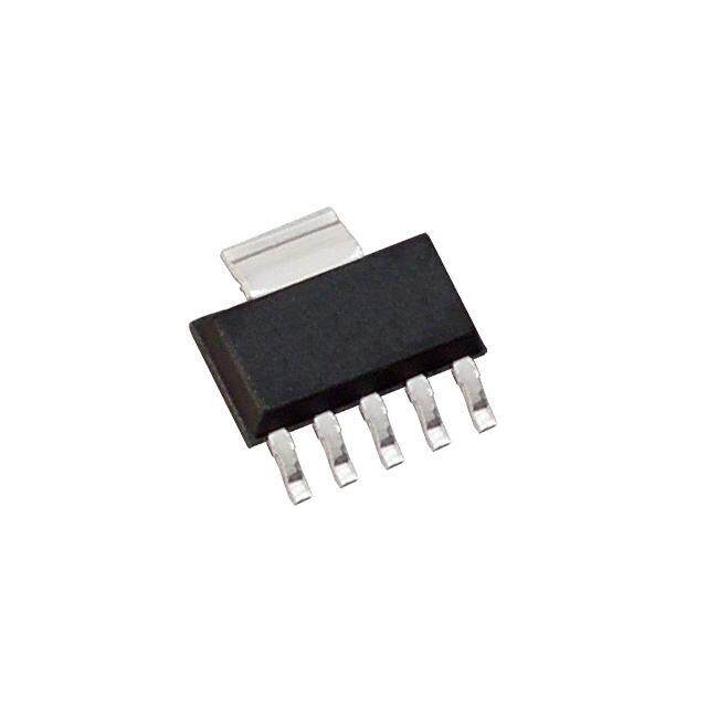
ICGOO电子元器件商城为您提供LP3985IM5-3.2/NOPB由Texas Instruments设计生产,在icgoo商城现货销售,并且可以通过原厂、代理商等渠道进行代购。 LP3985IM5-3.2/NOPB价格参考。Texas InstrumentsLP3985IM5-3.2/NOPB封装/规格:PMIC - 稳压器 - 线性, Linear Voltage Regulator IC Positive Fixed 1 Output 3.2V 150mA SOT-23-5。您可以下载LP3985IM5-3.2/NOPB参考资料、Datasheet数据手册功能说明书,资料中有LP3985IM5-3.2/NOPB 详细功能的应用电路图电压和使用方法及教程。
| 参数 | 数值 |
| 产品目录 | 集成电路 (IC)半导体 |
| 描述 | IC REG LDO 3.2V 0.15A SOT23-5低压差稳压器 150Ma Low Noise CMOS LDO |
| 产品分类 | |
| 品牌 | Texas Instruments |
| 产品手册 | |
| 产品图片 |
|
| rohs | 符合RoHS无铅 / 符合限制有害物质指令(RoHS)规范要求 |
| 产品系列 | 电源管理 IC,低压差稳压器,Texas Instruments LP3985IM5-3.2/NOPB- |
| 数据手册 | |
| 产品型号 | LP3985IM5-3.2/NOPB |
| PCN设计/规格 | |
| PSRR/纹波抑制—典型值 | 50 dB |
| 产品 | Mircopower Ultra Low-Dropout Low-Noise CMOS Voltage Regulator |
| 产品目录页面 | |
| 产品种类 | 低压差稳压器 |
| 供应商器件封装 | SOT-23-5 |
| 其它名称 | LP3985IM5-3.2/NOPBDKR |
| 制造商产品页 | http://www.ti.com/general/docs/suppproductinfo.tsp?distId=10&orderablePartNumber=LP3985IM5-3.2/NOPB |
| 包装 | Digi-Reel® |
| 商标 | Texas Instruments |
| 回动电压—最大值 | 100 mV |
| 安装类型 | 表面贴装 |
| 安装风格 | SMD/SMT |
| 封装 | Reel |
| 封装/外壳 | SC-74A,SOT-753 |
| 封装/箱体 | SOT-23-5 |
| 工作温度 | -40°C ~ 125°C |
| 工厂包装数量 | 1000 |
| 最大功率耗散 | 364 mW |
| 最大工作温度 | + 125 C |
| 最大输入电压 | 6 V |
| 最小工作温度 | - 40 C |
| 最小输入电压 | 2.5 V |
| 标准包装 | 1 |
| 电压-跌落(典型值) | 0.06V @ 150mA |
| 电压-输入 | 最高 6V |
| 电压-输出 | 3.2V |
| 电流-输出 | 150mA |
| 电流-限制(最小值) | 300mA |
| 稳压器拓扑 | 正,固定式 |
| 稳压器数 | 1 |
| 类型 | Low dropout low quiescent current regulator |
| 系列 | LP3985 |
| 线路调整率 | +/- 0.1 % |
| 设计资源 | http://www.digikey.com/product-highlights/cn/zh/texas-instruments-webench-design-center/3176 |
| 负载调节 | 0.0025 % |
| 输出电压 | 3.2 V |
| 输出电压容差 | +/- 3 % |
| 输出电流 | 150 mA |
| 输出端数量 | 1 Output |
| 输出类型 | Fixed |



PDF Datasheet 数据手册内容提取
Product Sample & Technical Tools & Support & Folder Buy Documents Software Community LP3985 SNVS087AE–OCTOBER2000–REVISEDMAY2015 LP3985 Micropower, 150-mA Low-Noise Ultra-Low-Dropout CMOS Voltage Regulator 1 Features 3 Description • InputVoltage:2.5Vto6V The LP3985 is designed for portable and wireless 1 applications with demanding performance and space • 100-mVMaximumDropoutwith150-mALoad requirements. LP3985 performance is optimized for • 150-mAVerifiedOutput battery-powered systems to deliver ultra low noise, • 50-dBPSRRat1kHzatV =V +0.2V extremely low dropout voltage, and low quiescent IN OUT current. Regulator ground current increases only • ≤1.5-μAQuiescentCurrentwhenShutDown slightlyindropout,furtherprolongingthebatterylife. • FastTurn-Ontime:200 μs(typ.) The LP3985 is stable with a small 1-µF ±30% • 30-μV OutputNoise(typical)over10Hzto100 RMS ceramicorhigh-qualitytantalumoutputcapacitor.The kHz DSBGA requires the smallest possible PC board area • −40°Cto125°CJunctionTemperatureRangefor - the total application circuit area can be less than 2 Operation mmx2.5mm,afractionofa1206casesize. • 2.5-V,2.6-V,2.7-V,2.8-V,2.85-V,2.9-V,3-V,3.1- An optional external bypass capacitor reduces the V,3.2-V,3.3-V,4.7-V,4.75-V,4.8-Vand5-V output noise without slowing down the load transient OutputsStandard response. Fast startup time is achieved by utilizing an • LogicControlledEnable internal power-on circuit that actively pre-charges the bypasscapacitor. • StablewithCeramicandHigh-QualityTantalum Capacitors Power supply rejection is better than 50 dB at low frequencies and starts to roll off at 1 kHz. High power • FastTurnon supply rejection is maintained down to low input • ThermalShutdownandShort-CircuitCurrentLimit voltagelevelscommontobatteryoperatedcircuits. 2 Applications The device is ideal for mobile phone and similar battery-powered wireless applications. It provides up • CDMACellularHandsets to 150 mA, from a 2.5-V to 6-V input. The LP3985 • WidebandCDMACellularHandsets consumes less than 1.5 µA in disable mode and has fastturn-ontimelessthan200 µs. • GSMCellularHandsets • PortableInformationAppliances The LP3985 is available with fixed output voltages from 2.5 V to 5 V. Contact Texas Instruments Sales space forspecificvoltageoptionneeds. SimplifiedSchematic DeviceInformation(1) 1(C3) 5(C1) PART PACKAGE BODYSIZE IN OUT NUMBER 1µF DSBGA(5) 1.502mmx1.045mm(MAX) 1µF LP3985 SOT-23(5) 2.90mmx1.60mm(NOM) LP3985 (1) For all available packages, see the Package Option Addendumattheendofthedatasheet. 3(A1) 4(A3) EN BYPASS * 2(B2) Pin Numbers in parenthesis indicate DSBGA package. * Optional Noise Reduction Capacitor. 1 An IMPORTANT NOTICE at the end of this data sheet addresses availability, warranty, changes, use in safety-critical applications, intellectualpropertymattersandotherimportantdisclaimers.PRODUCTIONDATA.
LP3985 SNVS087AE–OCTOBER2000–REVISEDMAY2015 www.ti.com Table of Contents 1 Features.................................................................. 1 7.4 DeviceFunctionalModes........................................14 2 Applications........................................................... 1 8 ApplicationandImplementation........................ 15 3 Description............................................................. 1 8.1 ApplicationInformation............................................15 4 RevisionHistory..................................................... 2 8.2 TypicalApplication .................................................15 5 PinConfigurationandFunctions......................... 3 9 PowerSupplyRecommendations...................... 18 6 Specifications......................................................... 4 10 Layout................................................................... 19 6.1 AbsoluteMaximumRatings......................................4 10.1 LayoutGuidelines.................................................19 6.2 ESDRatings..............................................................4 10.2 LayoutExamples...................................................19 6.3 RecommendedOperatingConditions.......................4 10.3 DSBGAMounting..................................................19 6.4 ThermalInformation..................................................4 10.4 DSBGALightSensitivity.......................................19 6.5 ElectricalCharacteristics...........................................5 11 DeviceandDocumentationSupport................. 21 6.6 TypicalPerformanceCharacteristics........................7 11.1 DocumentationSupport .......................................21 7 DetailedDescription............................................ 13 11.2 Trademarks...........................................................21 7.1 Overview.................................................................13 11.3 ElectrostaticDischargeCaution............................21 7.2 FunctionalBlockDiagram.......................................13 11.4 Glossary................................................................21 7.3 FeatureDescription.................................................13 12 Mechanical,Packaging,andOrderable Information........................................................... 21 4 Revision History NOTE:Pagenumbersforpreviousrevisionsmaydifferfrompagenumbersinthecurrentversion. ChangesfromRevisionAD(October2014)toRevisionAE Page • ChangedupdatepinnamestoTInomenclature;replaceHandlingRatingswithESDRatings ........................................... 1 • DeletedVoltageOptionstable-informationinPOA ............................................................................................................. 1 • AddedGNDastypeforgroundpins ..................................................................................................................................... 3 • AddedThermalConsiderationssub-section........................................................................................................................ 17 ChangesfromRevisionAC(May2013)toRevisionAD Page • AddedDeviceInformationandHandlingRatingtables,FeatureDescription,DeviceFunctionalModes,Application andImplementation,PowerSupplyRecommendations,Layout,DeviceandDocumentationSupport,and Mechanical,Packaging,andOrderableInformationsections;movedsomecurvestoApplicationCurvessection;add newThermalInformation........................................................................................................................................................ 1 ChangesfromRevisionAB(May2013)toRevisionAC Page • ChangedlayoutofNationalDataSheettoTIformat........................................................................................................... 20 2 SubmitDocumentationFeedback Copyright©2000–2015,TexasInstrumentsIncorporated ProductFolderLinks:LP3985
LP3985 www.ti.com SNVS087AE–OCTOBER2000–REVISEDMAY2015 5 Pin Configuration and Functions DBVPackage 5PinSOT-23 TopView EN GND IN 3 2 1 4 5 BYPASS OUT YZRPackage 5PinDSBGA TopView BYPASS IN A3 C3 GND B2 A1 C1 EN OUT PinFunctions PIN DSBGA SOT-23 TYPE DESCRIPTION NAME NUMBER(1) NUMBER BYPASS A3 4 I/O Optionalbypasscapacitorfornoisereduction EN A1 3 I Enableinputlogic,enablehigh GND B2 2 GND Commonground IN C3 1 I InputvoltageoftheLDO OUT C1 5 O OutputvoltageoftheLDO (1) ThepinnumberingschemefortheDSBGApackagewasrevisedinApril2002toconformtoJEDECstandard.Onlythepinnumbers wererevised.Nochangestothephysicallocationoftheinputs/outputsweremade.Forreferencepurposes,theobsoletenumbering schemehadVENaspin1,GNDaspin2,VOUTaspin3,VINaspin4,andBYPASSaspin5. Copyright©2000–2015,TexasInstrumentsIncorporated SubmitDocumentationFeedback 3 ProductFolderLinks:LP3985
LP3985 SNVS087AE–OCTOBER2000–REVISEDMAY2015 www.ti.com 6 Specifications 6.1 Absolute Maximum Ratings overoperatingfree-airtemperaturerange(unlessotherwisenoted) (1)(2)(3) MIN MAX UNIT IN,EN –0.3 6.5 V OUT −0.3 (V +0.3)<6.5 IN Junctiontemperature 150 Leadtemperature 235 °C Padtemperature(4) 235 SOT-23(5) 364 Maximumpowerdissipation mW DSBGA(5) 314 Storagetemperature,T –65 150 °C stg (1) StressesbeyondthoselistedunderAbsoluteMaximumRatingsmaycausepermanentdamagetothedevice.Thesearestressratings only,whichdonotimplyfunctionaloperationofthedeviceattheseoranyotherconditionsbeyondthoseindicatedunderRecommended OperatingConditions.Exposuretoabsolute-maximum-ratedconditionsforextendedperiodsmayaffectdevicereliability. (2) AllvoltagesarewithrespecttopotentialattheGNDpin. (3) IfMilitary/Aerospacespecifieddevicesarerequired,pleasecontacttheTexasInstrumentsSalesOffice/Distributorsforavailabilityand specifications. (4) AdditionalinformationonleadtemperatureandpadtemperaturecanbefoundinTexasInstrumentsApplicationNoteAN-1187Leadless LeadframePackage(LLP)(SNOA401). (5) TheAbsoluteMaximumpowerdissipationdependsontheambienttemperatureandcanbecalculatedusingtheformula:P =(T - D J T )/R ,whereT isthejunctiontemperature,T istheambienttemperature,andR isthejunction-to-ambientthermalresistance. A θJA J A θJA The364-mWratingforSOT23-5appearingunderAbsoluteMaximumRatingsresultsfromsubstitutingtheAbsoluteMaximumjunction temperature,150°CforT ,70°CforT ,and220°C/WforR .Morepowercanbedissipatedsafelyatambienttemperaturesbelow J A θJA 70°C.Lesspowercanbedissipatedsafelyatambienttemperaturesabove70°C.TheAbsoluteMaximumpowerdissipationcanbe increasedby4.5mWforeachdegreebelow70°C,anditmustbederatedby4.5mWforeachdegreeabove70°C. 6.2 ESD Ratings VALUE UNIT V Electrostaticdischarge Human-bodymodel(HBM),perANSI/ESDA/JEDECJS-001(1) ±2000 V (ESD) (1) JEDECdocumentJEP155statesthat500-VHBMallowssafemanufacturingwithastandardESDcontrolprocess. 6.3 Recommended Operating Conditions overoperatingfree-airtemperaturerange(unlessotherwisenoted) MIN MAX UNIT V Supplyinputvoltage 2.5(1) 6 V IN V ON/OFFinputvoltage 0 V V EN IN I Outputcurrent 150 mA OUT T Operatingjunctiontemperature −40 125 °C J (1) RecommendedminimumV isthegreaterof2.5-VorV +rateddropoutvoltage(max)foroperatingloadcurrent. IN OUT(MAX) 6.4 Thermal Information LP3985 THERMALMETRIC(1) SOT-23(DBV) DSBGA(YZR) UNIT 5PINS R Junction-to-ambientthermalresistance 220 255 θJA R Junction-to-case(top)thermalresistance 79.8 0.8 θJC(top) R Junction-to-boardthermalresistance 31.6 107.9 θJB °C/W ψ Junction-to-topcharacterizationparameter 3.1 0.5 JT ψ Junction-to-boardcharacterizationparameter 31.1 107.9 JB R Junction-to-case(bottom)thermalresistance N/A N/A θJC(bot) (1) Formoreinformationabouttraditionalandnewthermalmetrics,seetheICPackageThermalMetricsapplicationreport,SPRA953. 4 SubmitDocumentationFeedback Copyright©2000–2015,TexasInstrumentsIncorporated ProductFolderLinks:LP3985
LP3985 www.ti.com SNVS087AE–OCTOBER2000–REVISEDMAY2015 6.5 Electrical Characteristics Unlessotherwisespecified:V =V +0.5V,C =1μF,I =1mA,C =1μF,C =0.01μF.Minimum(MIN) IN OUT(nom) IN OUT OUT BYPASS andMaximum(MAX)valuesapplyover–40°C≤T ≤125°CandtypicalvaluesareT =25°C,unlessotherwiseindicated. J A (1)(2) PARAMETER TESTCONDITIONS MIN TYP MAX UNIT –2(3) 2(3) %of Outputvoltagetolerance I =1mA OUT –3 3 V OUT(nom) V =(V +0.5V)to6V, IN OUT(nom) Lineregulationerror For4.7-Vto5-Voptions –0.19 0.19 %/V ΔVOUT Forallotheroptions –0.1 0.1 I =1mAto150mA OUT 0.0025 0.005 %/mA Loadregulationerror(4) LP3985IM5(SOT23-5) LP3985(DSBGA) 0.0004 0.002 %/mA V =V +1V, OutputAClineregulation IN OUT(nom) 1.5 mV I =150mA(Figure1) P-P OUT V =V +0.2V, IN OUT(nom) f=1kHz, 50 dB I =50mA(Figure2) OUT PSRR Powersupplyrejectionratio V =V +0.2V, IN OUT(nom) ƒ=10kHz, 40 dB I =50mA(Figure2) OUT V =1.4V,I =0mA EN OUT For4.7-Vto5-Voptions 100 165 Forallotheroptions 85 150 I Quiescentcurrent V =1.4V,I =0to150mA µA Q EN OUT For4.7-Vto5-Voptions 155 250 Forallotheroptions 140 200 V =0.4V 0.003 1.5 EN I =1mA 0.4 2 mV OUT I =50mA 20 35 mV Dropoutvoltage(5) OUT I =100mA 45 70 mV OUT I =150mA 60 100 mV OUT OutputGrounded I Shortcircuitcurrentlimit 600 mA SC (SteadyState) I Peakoutputcurrent V ≥V –5% 300 550 mA OUT(PK) OUT OUT(nom) T Turnontime(6) C =0.01µF 200 µs ON BYPASS Outputnoisevoltage(7) BW=10Hzto100kHz, 30 µV en COUT=1µF RMS Outputnoisedensity C =0 230 nV/√Hz BP I MaximuminputcurrentatEN V =0.4VandV =6V ±1 nA EN EN IN Maximumlow-levelinput V V V =2.5Vto6V 0.4 IL voltageatEN IN Minimumhigh-levelinput V V V =2.5Vto6V 1.4 IH voltageatEN IN Thermalshutdown °C 160 TSD temperature Thermalshutdownhysteresis 20 °C (1) Alllimitsareverified.Allelectricalcharacteristicshavingroom-temperaturelimitsaretestedduringproductionwithT =25°Cor A correlatedusingStatisticalQualityControl(SQC)methods.Allhotandcoldlimitsarespecifiedbycorrelatingtheelectrical characteristicstoprocessandtemperaturevariationsandapplyingstatisticalprocesscontrol. (2) Thetargetoutputvoltage,whichislabeledV ,isthedesiredvoltageoption. OUT(NOM) (3) T =25°Conly. A (4) Anincreaseintheloadcurrentresultsinaslightdecreaseintheoutputvoltageandviceversa. (5) Dropoutvoltageistheinput-to-outputvoltagedifferenceatwhichtheoutputvoltageis100mVbelowitsnominalvalue.Thisspecification doesnotapplyforinputvoltagesbelow2.5V. (6) TurnontimeistimemeasuredbetweentheenableinputjustexceedingV andtheoutputvoltagejustreaching95%ofitsnominal IH value. (7) Theoutputnoisevarieswithoutputvoltageoption.The30µV ismeasuredwith2.5-Vvoltageoption.Tocalculateanapproximated RMS outputnoiseforotheroptions,usetheequation:(30µV )(X)/2.5,whereXisthevoltageoptionvalue. RMS Copyright©2000–2015,TexasInstrumentsIncorporated SubmitDocumentationFeedback 5 ProductFolderLinks:LP3985
LP3985 SNVS087AE–OCTOBER2000–REVISEDMAY2015 www.ti.com Figure1. LineTransientInputTestSignal Figure2. PSRRInputTestSignal 6 SubmitDocumentationFeedback Copyright©2000–2015,TexasInstrumentsIncorporated ProductFolderLinks:LP3985
LP3985 www.ti.com SNVS087AE–OCTOBER2000–REVISEDMAY2015 6.6 Typical Performance Characteristics Unlessotherwisespecified,C =C =1µFceramic,C =0.01µF,V =V +0.2V,T =25°C,ENpinistiedto IN OUT BYPASS IN OUT A V . IN VIN = VOUT + 0.5V 0.4 )% ( E 0 G N A H C TU -0.4 O V -0.8 -50 -25 0 25 50 75 100 125 TEMPERATURE (°C) Figure3.OutputVoltageChangevsTemperature Figure4.DropoutVoltagevsLoadCurrent Figure5.GroundCurrentvsLoadCurrent Figure6.GroundCurrentvsVINat25°C Figure7.GroundCurrentvsV at−40°C Figure8.GroundCurrentvsV at125°C IN IN Copyright©2000–2015,TexasInstrumentsIncorporated SubmitDocumentationFeedback 7 ProductFolderLinks:LP3985
LP3985 SNVS087AE–OCTOBER2000–REVISEDMAY2015 www.ti.com Typical Performance Characteristics (continued) Unlessotherwisespecified,C =C =1µFceramic,C =0.01µF,V =V +0.2V,T =25°C,ENpinistiedto IN OUT BYPASS IN OUT A V . IN Figure9.ShortCircuitCurrent(DSBGA) Figure10.ShortCircuitCurrent(DSBGA) Figure11.ShortCircuitCurrent(SOT) Figure12.ShortCircuitCurrent(SOT) Figure13.ShortCircuitCurrent(SOT) Figure14.ShortCircuitCurrent(SOT) 8 SubmitDocumentationFeedback Copyright©2000–2015,TexasInstrumentsIncorporated ProductFolderLinks:LP3985
LP3985 www.ti.com SNVS087AE–OCTOBER2000–REVISEDMAY2015 Typical Performance Characteristics (continued) Unlessotherwisespecified,C =C =1µFceramic,C =0.01µF,V =V +0.2V,T =25°C,ENpinistiedto IN OUT BYPASS IN OUT A V . IN Figure15.ShortCircuitCurrent(DSBGA) Figure16.ShortCircuitCurrent(DSBGA) V =V +0.2V IN OUT Figure17.OutputNoiseSpectralDensity Figure18.RippleRejection V =V +1V V =5V IN OUT IN Figure19.RippleRejection Figure20.RippleRejection Copyright©2000–2015,TexasInstrumentsIncorporated SubmitDocumentationFeedback 9 ProductFolderLinks:LP3985
LP3985 SNVS087AE–OCTOBER2000–REVISEDMAY2015 www.ti.com Typical Performance Characteristics (continued) Unlessotherwisespecified,C =C =1µFceramic,C =0.01µF,V =V +0.2V,T =25°C,ENpinistiedto IN OUT BYPASS IN OUT A V . IN VIN=VOUT+0.2V VIN=VOUT+0.2V Figure21.Start-upTime Figure22.Start-upTime V =4.2V V =V +0.2V IN IN OUT Figure23.Start-upTime Figure24.Start-upTime V =4.2V IN Figure25.Start-upTime Figure26.LineTransientResponse 10 SubmitDocumentationFeedback Copyright©2000–2015,TexasInstrumentsIncorporated ProductFolderLinks:LP3985
LP3985 www.ti.com SNVS087AE–OCTOBER2000–REVISEDMAY2015 Typical Performance Characteristics (continued) Unlessotherwisespecified,C =C =1µFceramic,C =0.01µF,V =V +0.2V,T =25°C,ENpinistiedto IN OUT BYPASS IN OUT A V . IN V =3.2V IN Figure27.LineTransientResponse Figure28.LoadTransientResponse V =4.2V V =3.2V IN IN Figure29.LoadTransientResponse Figure30.LoadTransientResponse V =V +0.2V V =4.2V IN OUT IN Figure32.EnableResponse Figure31.LoadTransientResponse Copyright©2000–2015,TexasInstrumentsIncorporated SubmitDocumentationFeedback 11 ProductFolderLinks:LP3985
LP3985 SNVS087AE–OCTOBER2000–REVISEDMAY2015 www.ti.com Typical Performance Characteristics (continued) Unlessotherwisespecified,C =C =1µFceramic,C =0.01µF,V =V +0.2V,T =25°C,ENpinistiedto IN OUT BYPASS IN OUT A V . IN V =V +0.2V V =4.2V IN OUT IN Figure33.EnableResponse Figure34.EnableResponse V =4.2V V =V +0.2V IN IN OUT Figure35.OutputImpedance Figure36.OutputImpedance 12 SubmitDocumentationFeedback Copyright©2000–2015,TexasInstrumentsIncorporated ProductFolderLinks:LP3985
LP3985 www.ti.com SNVS087AE–OCTOBER2000–REVISEDMAY2015 7 Detailed Description 7.1 Overview The LP3985 family of fixed-output, ultra-low-dropout and low noise regulators offers exceptional, cost-effective performance for battery powered applications. Available in output voltages from 2.5 V to 5 V, the family is capable of delivering 150-mA continuous load current. Standard regulator features, such as overcurrent and overtemperatureprotection,arealsoincluded. TheLP3985containsseveralfeaturestofacilitatebatterypowereddesigns: •Multiplevoltageoptions •Lowdropoutvoltage,typicaldropoutof60mVat150-mAloadcurrent •Lowquiescentcurrentandlowgroundcurrent,typically140 μAat150-mAload,and85-μAat0-mAload • A shutdown feature is available, allowing the regulator to consume only 0.003 µA typically when the EN pin is pulledlow • Overtemperature protection and overcurrent protection circuitry is designed to safeguard the device during unexpectedconditions • Enhanced stability: The LP3985 is stable with output capacitor, which allows the use of ceramic capacitors on theoutput •Powersupplyrejectionisbetterthan50dBatlowfrequenciesandstartstorolloffat1kHz. • Low noise: A BYPASS pin allows for low-noise operation, with a typical output noise of 30 µV , with the use RMS ofa10-nFbypasscapacitor. 7.2 Functional Block Diagram IN OUT EN ON t 1.4V Vreference Fast Turnon 1.23V Circuit R1 d OFF 0.4V BYPASS R2 Overcurrent & Thermal Protection GND 7.3 Feature Description 7.3.1 No-LoadStability The LP3985 will remain stable and in regulation with no external load. This is specially important in CMOS RAM keep-aliveapplications. 7.3.2 On/OffInputOperation TheLP3985isturnedoffbypullingtheENpinlow,andturnedonbypullingithigh.Ifthisfeatureisnotused,the EN pin should be tied to V to keep the regulator output on at all time. To assure proper operation, the signal IN source used to drive the EN input must be able to swing above and below the specified turnon/turnoff voltage thresholdslistedinElectricalCharacteristicsunderV andV . IL IH Copyright©2000–2015,TexasInstrumentsIncorporated SubmitDocumentationFeedback 13 ProductFolderLinks:LP3985
LP3985 SNVS087AE–OCTOBER2000–REVISEDMAY2015 www.ti.com Feature Description (continued) 7.3.3 FastOn-Time The LP3985 output is turned on after V voltage reaches its final value (1.23 V, nominal). To speed up this REF process, the noise reduction capacitor at the BYPASS pin is charged with an internal 70-µA current source. The current source is turned off when the bandgap voltage reaches approximately 95% of its final value. The turnon time is determined by the time constant of the bypass capacitor. The smaller the capacitor value, the shorter the turn on time, but less noise gets reduced. As a result, turn on time and noise reduction need to be taken into designconsiderationwhenchoosingthevalueofthebypasscapacitor. 7.4 Device Functional Modes 7.4.1 OperationwithV +0.3V ≤ V ≤6V OUT(TARGET) IN The device operates if the input voltage is equal to, or exceeds, V + 0.3 V. At input voltages below the OUT(TARGET) minimumV requirement,thedevicesdoesnotoperatecorrectly,andoutputvoltagemaynotreachtargetvalue. IN 7.4.2 OperationUsingtheENPin IfthevoltageontheENpinislessthan0.4V,thedeviceisdisabled,andinthisstateshutdowncurrentdoesnot exceed1.5μA.RaisingV above1.4Vinitiatesthestart-upsequenceofthedevice. EN 14 SubmitDocumentationFeedback Copyright©2000–2015,TexasInstrumentsIncorporated ProductFolderLinks:LP3985
LP3985 www.ti.com SNVS087AE–OCTOBER2000–REVISEDMAY2015 8 Application and Implementation NOTE Information in the following applications sections is not part of the TI component specification, and TI does not warrant its accuracy or completeness. TI’s customers are responsible for determining suitability of components for their purposes. Customers should validateandtesttheirdesignimplementationtoconfirmsystemfunctionality. 8.1 Application Information The LP3985 can provide 150-mA output current with 2.5-V to 6-V input. It is stable with a small 1-µF ±30% ceramic or high-quality tantalum output capacitor. The DSBGA requires the smallest possible PC board area – the total application circuit area can be less than 2 mm x 2.5 mm, a fraction of a 1206 case size. An optional external bypass capacitor reduces the output noise without slowing down the load transient response. Fast startup time is achieved by utilizing an internal power-on circuit that actively pre-charges the bypass capacitor. Typical output noise is 30 µV at frequencies from 10 Hz to 100 kHz. Typical power RMS supplyrejectionis50dBat1kHz. 8.2 Typical Application 1(C3) 5(C1) IN OUT 1µF 1µF LP3985 3(A1) 4(A3) EN BYPASS * 2(B2) Pin Numbers in parenthesis indicate DSBGA package. * Optional Noise Reduction Capacitor. Figure37. LP3985TypicalApplication 8.2.1 DesignRequirements DESIGNPARAMETERS VALUE Inputvoltage 4.2V,±10%providedbytheDC-DCconverterswitchingat1MHz Outputvoltage 3V,±5% Outputcurrent 150mA(maximum) RMSnoise,10Hzto100kHz 30μV RMS PSRRat1kHz 50dB 8.2.2 DetailedDesignProcedure 8.2.2.1 ExternalCapacitors Like any low-dropout regulator, the LP3985 requires external capacitors for regulator stability. The LP3985 is specifically designed for portable applications requiring minimum board space and smallest components. These capacitorsmustbecorrectlyselectedforgoodperformance. 8.2.2.2 InputCapacitor An input capacitance of approximately 1 µF is required between the LP3985 input pin and ground (the amount of thecapacitancemaybeincreasedwithoutlimit). Copyright©2000–2015,TexasInstrumentsIncorporated SubmitDocumentationFeedback 15 ProductFolderLinks:LP3985
LP3985 SNVS087AE–OCTOBER2000–REVISEDMAY2015 www.ti.com This capacitor must be located a distance of not more than 1 cm from the input pin and returned to a clean analog ground. A ceramic capacitor is recommended although a good quality tantalum or film capacitor may be usedattheinput. NOTE Tantalum capacitors can suffer catastrophic failures due to surge current when connected to a low-impedance source of power (like a battery or a very large capacitor). If a tantalum capacitor is used at the input, it must be verified by the manufacturer to have a surge currentratingsufficientfortheapplication. There are no requirements for the ESR on the input capacitor, but tolerance and temperature coefficient must be considered when selecting the capacitor to ensure the capacitance will remain within the operational range over thefullrangeoftemperatureandoperatingconditions. 8.2.2.3 OutputCapacitor Correctselectionoftheoutputcapacitorisimportanttoensurestableoperationintheintendedapplication. The output capacitor must meet all the requirements specified in the recommended capacitor table over all conditions in the application. These conditions include DC-bias, frequency and temperature. Unstable operation will result if the capacitance drops below the minimum specified value. (See the next section Capacitor Characteristics). The LP3985 is designed specifically to work with very small ceramic output capacitors. A 1-µF ceramic capacitor (dialectric type X7R) with ESR between 5 mΩ to 500 mΩ is suitable in the LP3985 application circuit. X5R capacitors may be used but have a narrower temperature range. With these and other capacitor types (Y5V, Z6U) that may be used, selection is dependant on the range of operating conditions and temperature range for thatapplication.(seeCapacitorCharacteristics ). It may also be possible to use tantalum or film capacitors at the output, but these are not as attractive for reasonsofsizeandcost(seeCapacitorCharacteristics). It is also recommended that the output capacitor be placed within 1 cm from the output pin and returned to a cleangroundline. 8.2.2.4 CapacitorCharacteristics The LP3985 is designed to work with ceramic capacitors on the output to take advantage of the benefits they offer: for capacitance values in the range of 1 µF to 4.7 µF, ceramic capacitors are the smallest, least expensive, and have the lowest ESR values (which makes them best for eliminating high frequency noise). The ESR of a typical 1-µF ceramic capacitor is in the range of 20 mΩ to 40 mΩ, which easily meets the ESR requirement for stabilitybytheLP3985. For both input and output capacitors careful interpretation of the capacitor specification is required to ensure correct device operation. The capacitor value can change greatly dependant on the conditions of operation and capacitortype. In particular the output capacitor selection should take account of all the capacitor parameters to ensure that the specification is met within the application. Capacitance value can vary with DC bias conditions as well as temperature and frequency of operation. Capacitor values will also show some decrease over time due to aging. The capacitor parameters are also dependant on the particular case size with smaller sizes giving poorer performance figures in general. As an example Figure 38 shows a typical graph showing a comparison of capacitor case sizes in a Capacitance vs. DC Bias plot. As shown in the graph, as a result of the DC Bias condition the capacitance value may drop below the minimum capacitance value given in the recommended capacitor table (0.7 µF in this case). Note that the graph shows the capacitance out of spec for the 0402 case size capacitor at higher bias voltages. It is therefore recommended that the capacitor manufacturers' specifications for the nominal value capacitor are consulted for all conditions as some capacitor sizes (for example,0402)maynotbesuitableintheactualapplication. 16 SubmitDocumentationFeedback Copyright©2000–2015,TexasInstrumentsIncorporated ProductFolderLinks:LP3985
LP3985 www.ti.com SNVS087AE–OCTOBER2000–REVISEDMAY2015 )F 0603, 10V, X5R P 1 100% L A N IM O 80% N fo % ( E 60% U L 0402, 6.3V, X5R A V P 40% A C 20% 0 1.0 2.0 3.0 4.0 5.0 DC BIAS (V) Figure38. GraphShowingATypicalVariationInCapacitancevsDCBias The ceramic capacitor's capacitance can vary with temperature. The capacitor type X7R, which operates over a temperature range of −55°C to 125°C, will only vary the capacitance to within ±15%. The capacitor type X5R has a similar tolerance over a reduced temperature range of −55°C to 85°C. Most large value ceramic capacitors (around 2.2 µF) are manufactured with Z5U or Y5V temperature characteristics. Their capacitance can drop by more than 50% as the temperature goes from 25°C to 85°C. Therefore X7R is recommended over Z5U and Y5V inapplicationswheretheambienttemperaturewillchangesignificantlyaboveorbelow25°C. Tantalum capacitors are less desirable than ceramic for use as output capacitors because they are more expensivewhencomparingequivalentcapacitanceandvoltageratingsinthe1-µFto4.7-µFrange. Another important consideration is that tantalum capacitors have higher ESR values than equivalent size ceramics. This means that while it may be possible to find a tantalum capacitor with an ESR value within the stable range, it would have to be larger in capacitance (which means bigger and more costly ) than a ceramic capacitor with the same ESR value. It should also be noted that the ESR of a typical tantalum will increase about 2:1asthetemperaturegoesfrom25°Cdownto −40°C,sosomeguardbandmustbeallowed. 8.2.2.5 NoiseBypassCapacitor Connecting a 0.01-µF capacitor between the CBYPASS pin and ground significantly reduces noise on the regulator output. This cap is connected directly to a high impedance node in the band gap reference circuit. Any significant loading on this node will cause a change on the regulated output voltage. For this reason, DC leakage currentthroughthispinmustbekeptaslowaspossibleforbestoutputvoltageaccuracy. The types of capacitors best suited for the noise bypass capacitor are ceramic and film. High-quality ceramic capacitors with either NPO or COG dielectric typically have very low leakage. Polypropolene and polycarbonate filmcapacitorsareavailableinsmallsurface-mountpackagesandtypicallyhaveextremelylowleakagecurrent. Unlike many other LDOs, addition of a noise reduction capacitor does not effect the load transient response of thedevice. 8.2.2.6 ThermalConsiderations CAUTION Due to the limited power dissipation characteristics of the available SOT-23 (DBV) and DSBGA (YZR) packages, all possible combinations of output current (I ), input OUT voltage (VIN), output voltage (V ), and ambient temperatures (T ) cannot be OUT A ensured. Powerdissipation,P iscalculatedfromthefollowingformula:P =((V –V )×I ). D D IN OUT OUT Copyright©2000–2015,TexasInstrumentsIncorporated SubmitDocumentationFeedback 17 ProductFolderLinks:LP3985
LP3985 SNVS087AE–OCTOBER2000–REVISEDMAY2015 www.ti.com The LP3985 regulator has internal thermal limiting designed to protect the device during overload conditions. For continuous normal conditions, the recommended maximum operating junction temperature is 125°C. It is important to give careful consideration to all sources of thermal resistance from junction to ambient. Additional heatsourcesmountednearbymustalsobeconsidered. For surface-mount devices, heat sinking is accomplished by using the heat-spreading capabilities of the PC board and its copper traces. Copper board stiffeners and plated through-holes can also be used to spread the heat generated by power devices. Example: Given an output voltage of 3.3 V, an input voltage range of 4 V to 6 V, a maximum output current of 100 mA, and a maximum ambient temperature of 50°C, what is the maximum operatingjunctiontemperature?Thepowerdissipatedbythedeviceisfoundusingtheformula: P = ((V ± V ) × I ) D(MAX) IN(MAX) OUT OUT(MAX) where • I =100mA OUT(MAX) • V =6V IN(MAX) • V =3.3V (1) OUT Forexample,P =((6V–3.3V) × 100mA)=0.27W. D(MAX) Using the 5-pin SOT-23 (DBV) package, the LP3985 junction-to-ambient thermal resistance (RθJA) has a rating of 220°C/W using the standard JEDEC JESD51-7 PCB (High-K) circuit board. The junction temperature rise aboveambientisfoundusingtheformula: T =P ×R ; RISE D(MAX) θJA forexample,T =50°C+59.4°C=109.4°C. J(MAX) 8.2.3 ApplicationCurves V =4.2V V =4.2V IN IN Figure39.Start-upTime Figure40.EnableResponse 9 Power Supply Recommendations TheLP3985isdesignedtooperatefromaninputvoltagesupplyrangebetween2.5Vand6V.Theinput-voltage range provides adequate headroom in order for the device to have a regulated output. This input supply must be well regulated. If the input supply is noisy, additional input capacitors with low ESR can help to improve the outputnoiseperformance. 18 SubmitDocumentationFeedback Copyright©2000–2015,TexasInstrumentsIncorporated ProductFolderLinks:LP3985
LP3985 www.ti.com SNVS087AE–OCTOBER2000–REVISEDMAY2015 10 Layout 10.1 Layout Guidelines For best overall performance, place all circuit components on the same side of the circuit board and as near as practical to the respective LDO pin connections. Place ground return connections to the input and output capacitor, and to the LDO ground pin as close to each other as possible, connected by a wide, component-side, copper surface. The use of vias and long traces to create LDO circuit connections is strongly discouraged and negatively affects system performance. This grounding and layout scheme minimizes inductive parasitics, and thereby reduces load-current transients, minimizes noise, and increases circuit stability. A ground reference plane is also recommended and is either embedded in the PCB itself or located on the bottom side of the PCB opposite the components. This reference plane serves to assure accuracy of the output voltage, shield noise, and behaves similar to a thermal plane to spread (or sink) heat from the LDO device. In most applications, this groundplaneisnecessarytomeetthermalrequirements. 10.2 Layout Examples VIN VOUT Input IN OUT Output Capacitor Capacitor GND Ground Bypass Capacitor EN BYPASS Figure41. LP3985SOT-23PackageTypicalLayout IN OUT Input Output Capacitor Capacitor C3 C1 GND B2 Bypass Capacitor A3 A1 BYPASS EN Figure42. LP3985DSBGAPackageTypicalLayout 10.3 DSBGA Mounting The DSBGA package requires specific mounting techniques which are detailed in Texas Instruments Application Note 1112 DSBGA Wafer Level Chip Scale Package (SNVA009). Referring to the section Surface Mount Technology (SMT) Assembly Considerations, it should be noted that the pad style which must be used with the 5-bumppackageisNSMD(non-soldermaskdefined)type. For best results during assembly, alignment ordinals on the PC board may be used to facilitate placement of the DSBGAdevice. 10.4 DSBGA Light Sensitivity Exposing the DSBGA device to direct sunlight will cause mis-operation of the device. Light sources such as halogenlampscaneffectelectricalperformanceifbroughtneartothedevice. Copyright©2000–2015,TexasInstrumentsIncorporated SubmitDocumentationFeedback 19 ProductFolderLinks:LP3985
LP3985 SNVS087AE–OCTOBER2000–REVISEDMAY2015 www.ti.com DSBGA Light Sensitivity (continued) The wavelengths which have most detrimental effect are reds and infra-reds, which means that the fluorescent lighting used inside most buildings has very little effect on performance. A DSBGA test board was brought to within 1 cm of a fluorescent desk lamp and the effect on the regulated output voltage was negligible, showing a deviationoflessthan0.1%fromnominal. 20 SubmitDocumentationFeedback Copyright©2000–2015,TexasInstrumentsIncorporated ProductFolderLinks:LP3985
LP3985 www.ti.com SNVS087AE–OCTOBER2000–REVISEDMAY2015 11 Device and Documentation Support 11.1 Documentation Support 11.1.1 RelatedDocumentation Forrelateddocumentation,seethefollowing: • TexasInstrumentsApplicationNoteAN-1187 LeadlessLeadframePackage(LLP)(SNOA401). • TexasInstrumentsApplicationNoteAN-1112 DSBGAWaferLevelChipScalePackage (SNVA009). 11.2 Trademarks Alltrademarksarethepropertyoftheirrespectiveowners. 11.3 Electrostatic Discharge Caution This integrated circuit can be damaged by ESD. Texas Instruments recommends that all integrated circuits be handled with appropriateprecautions.Failuretoobserveproperhandlingandinstallationprocedurescancausedamage. ESDdamagecanrangefromsubtleperformancedegradationtocompletedevicefailure.Precisionintegratedcircuitsmaybemore susceptibletodamagebecauseverysmallparametricchangescouldcausethedevicenottomeetitspublishedspecifications. 11.4 Glossary SLYZ022—TIGlossary. Thisglossarylistsandexplainsterms,acronyms,anddefinitions. 12 Mechanical, Packaging, and Orderable Information The following pages include mechanical, packaging, and orderable information. This information is the most current data available for the designated devices. This data is subject to change without notice and revision of thisdocument.Forbrowser-basedversionsofthisdatasheet,refertotheleft-handnavigation. Copyright©2000–2015,TexasInstrumentsIncorporated SubmitDocumentationFeedback 21 ProductFolderLinks:LP3985
PACKAGE OPTION ADDENDUM www.ti.com 6-Feb-2020 PACKAGING INFORMATION Orderable Device Status Package Type Package Pins Package Eco Plan Lead/Ball Finish MSL Peak Temp Op Temp (°C) Device Marking Samples (1) Drawing Qty (2) (6) (3) (4/5) LP3985IM5-2.5 NRND SOT-23 DBV 5 1000 TBD Call TI Call TI -40 to 125 LCSB LP3985IM5-2.5/NOPB ACTIVE SOT-23 DBV 5 1000 Green (RoHS SN Level-1-260C-UNLIM -40 to 125 LCSB & no Sb/Br) LP3985IM5-2.7/NOPB ACTIVE SOT-23 DBV 5 1000 Green (RoHS SN Level-1-260C-UNLIM -40 to 125 LCUB & no Sb/Br) LP3985IM5-2.8/NOPB ACTIVE SOT-23 DBV 5 1000 Green (RoHS SN Level-1-260C-UNLIM -40 to 125 LCJB & no Sb/Br) LP3985IM5-2.9/NOPB ACTIVE SOT-23 DBV 5 1000 Green (RoHS SN Level-1-260C-UNLIM -40 to 125 LCYB & no Sb/Br) LP3985IM5-3.0/NOPB ACTIVE SOT-23 DBV 5 1000 Green (RoHS SN Level-1-260C-UNLIM -40 to 125 LCRB & no Sb/Br) LP3985IM5-3.2/NOPB ACTIVE SOT-23 DBV 5 1000 Green (RoHS SN Level-1-260C-UNLIM -40 to 125 LDPB & no Sb/Br) LP3985IM5-3.3 NRND SOT-23 DBV 5 1000 TBD Call TI Call TI -40 to 125 LDQB LP3985IM5-3.3/NOPB ACTIVE SOT-23 DBV 5 1000 Green (RoHS SN Level-1-260C-UNLIM -40 to 125 LDQB & no Sb/Br) LP3985IM5-4.7/NOPB ACTIVE SOT-23 DBV 5 1000 Green (RoHS SN Level-1-260C-UNLIM -40 to 125 LDRB & no Sb/Br) LP3985IM5-5.0/NOPB ACTIVE SOT-23 DBV 5 1000 Green (RoHS SN Level-1-260C-UNLIM -40 to 125 LDSB & no Sb/Br) LP3985IM5X-2.5/NOPB ACTIVE SOT-23 DBV 5 3000 Green (RoHS SN Level-1-260C-UNLIM -40 to 125 LCSB & no Sb/Br) LP3985IM5X-2.8/NOPB ACTIVE SOT-23 DBV 5 3000 Green (RoHS SN Level-1-260C-UNLIM -40 to 125 LCJB & no Sb/Br) LP3985IM5X-285/NOPB ACTIVE SOT-23 DBV 5 3000 Green (RoHS SN Level-1-260C-UNLIM -40 to 125 LCXB & no Sb/Br) LP3985IM5X-3.0 NRND SOT-23 DBV 5 3000 TBD Call TI Call TI -40 to 125 LCRB LP3985IM5X-3.0/NOPB ACTIVE SOT-23 DBV 5 3000 Green (RoHS SN Level-1-260C-UNLIM -40 to 125 LCRB & no Sb/Br) LP3985IM5X-3.3/NOPB ACTIVE SOT-23 DBV 5 3000 Green (RoHS SN Level-1-260C-UNLIM -40 to 125 LDQB & no Sb/Br) LP3985IM5X-4.7/NOPB ACTIVE SOT-23 DBV 5 3000 Green (RoHS SN Level-1-260C-UNLIM -40 to 125 LDRB & no Sb/Br) Addendum-Page 1
PACKAGE OPTION ADDENDUM www.ti.com 6-Feb-2020 Orderable Device Status Package Type Package Pins Package Eco Plan Lead/Ball Finish MSL Peak Temp Op Temp (°C) Device Marking Samples (1) Drawing Qty (2) (6) (3) (4/5) LP3985IM5X-5.0/NOPB ACTIVE SOT-23 DBV 5 3000 Green (RoHS SN Level-1-260C-UNLIM -40 to 125 LDSB & no Sb/Br) LP3985ITL-2.5/NOPB ACTIVE DSBGA YZR 5 250 Green (RoHS SNAGCU Level-1-260C-UNLIM -40 to 125 5 & no Sb/Br) LP3985ITL-2.6/NOPB ACTIVE DSBGA YZR 5 250 Green (RoHS SNAGCU Level-1-260C-UNLIM -40 to 125 5 & no Sb/Br) LP3985ITL-2.7/NOPB ACTIVE DSBGA YZR 5 250 Green (RoHS SNAGCU Level-1-260C-UNLIM -40 to 125 5 & no Sb/Br) LP3985ITL-2.8/NOPB ACTIVE DSBGA YZR 5 250 Green (RoHS SNAGCU Level-1-260C-UNLIM -40 to 125 5 & no Sb/Br) LP3985ITL-2.9/NOPB ACTIVE DSBGA YZR 5 250 Green (RoHS SNAGCU Level-1-260C-UNLIM -40 to 125 5 & no Sb/Br) LP3985ITL-285/NOPB ACTIVE DSBGA YZR 5 250 Green (RoHS SNAGCU Level-1-260C-UNLIM -40 to 125 5 & no Sb/Br) LP3985ITL-3.0/NOPB ACTIVE DSBGA YZR 5 250 Green (RoHS SNAGCU Level-1-260C-UNLIM -40 to 125 5 & no Sb/Br) LP3985ITL-3.1/NOPB ACTIVE DSBGA YZR 5 250 Green (RoHS SNAGCU Level-1-260C-UNLIM -40 to 125 5 & no Sb/Br) LP3985ITL-3.3/NOPB ACTIVE DSBGA YZR 5 250 Green (RoHS SNAGCU Level-1-260C-UNLIM -40 to 125 5 & no Sb/Br) LP3985ITL-4.8/NOPB ACTIVE DSBGA YZR 5 250 Green (RoHS SNAGCU Level-1-260C-UNLIM 5 & no Sb/Br) LP3985ITL-5.0/NOPB ACTIVE DSBGA YZR 5 250 Green (RoHS SNAGCU Level-1-260C-UNLIM -40 to 125 5 & no Sb/Br) LP3985ITLX-2.5/NOPB ACTIVE DSBGA YZR 5 3000 Green (RoHS SNAGCU Level-1-260C-UNLIM -40 to 125 5 & no Sb/Br) LP3985ITLX-2.7/NOPB ACTIVE DSBGA YZR 5 3000 Green (RoHS SNAGCU Level-1-260C-UNLIM -40 to 125 5 & no Sb/Br) LP3985ITLX-2.8/NOPB ACTIVE DSBGA YZR 5 3000 Green (RoHS SNAGCU Level-1-260C-UNLIM -40 to 125 5 & no Sb/Br) LP3985ITLX-285/NOPB ACTIVE DSBGA YZR 5 3000 Green (RoHS SNAGCU Level-1-260C-UNLIM -40 to 125 5 & no Sb/Br) LP3985ITLX-3.0/NOPB ACTIVE DSBGA YZR 5 3000 Green (RoHS SNAGCU Level-1-260C-UNLIM -40 to 125 5 & no Sb/Br) LP3985ITLX-3.1/NOPB ACTIVE DSBGA YZR 5 3000 Green (RoHS SNAGCU Level-1-260C-UNLIM -40 to 125 5 & no Sb/Br) Addendum-Page 2
PACKAGE OPTION ADDENDUM www.ti.com 6-Feb-2020 Orderable Device Status Package Type Package Pins Package Eco Plan Lead/Ball Finish MSL Peak Temp Op Temp (°C) Device Marking Samples (1) Drawing Qty (2) (6) (3) (4/5) LP3985ITLX-3.3/NOPB ACTIVE DSBGA YZR 5 3000 Green (RoHS SNAGCU Level-1-260C-UNLIM -40 to 125 5 & no Sb/Br) LP3985ITLX-5.0/NOPB ACTIVE DSBGA YZR 5 3000 Green (RoHS SNAGCU Level-1-260C-UNLIM -40 to 125 5 & no Sb/Br) (1) The marketing status values are defined as follows: ACTIVE: Product device recommended for new designs. LIFEBUY: TI has announced that the device will be discontinued, and a lifetime-buy period is in effect. NRND: Not recommended for new designs. Device is in production to support existing customers, but TI does not recommend using this part in a new design. PREVIEW: Device has been announced but is not in production. Samples may or may not be available. OBSOLETE: TI has discontinued the production of the device. (2) RoHS: TI defines "RoHS" to mean semiconductor products that are compliant with the current EU RoHS requirements for all 10 RoHS substances, including the requirement that RoHS substance do not exceed 0.1% by weight in homogeneous materials. Where designed to be soldered at high temperatures, "RoHS" products are suitable for use in specified lead-free processes. TI may reference these types of products as "Pb-Free". RoHS Exempt: TI defines "RoHS Exempt" to mean products that contain lead but are compliant with EU RoHS pursuant to a specific EU RoHS exemption. Green: TI defines "Green" to mean the content of Chlorine (Cl) and Bromine (Br) based flame retardants meet JS709B low halogen requirements of <=1000ppm threshold. Antimony trioxide based flame retardants must also meet the <=1000ppm threshold requirement. (3) MSL, Peak Temp. - The Moisture Sensitivity Level rating according to the JEDEC industry standard classifications, and peak solder temperature. (4) There may be additional marking, which relates to the logo, the lot trace code information, or the environmental category on the device. (5) Multiple Device Markings will be inside parentheses. Only one Device Marking contained in parentheses and separated by a "~" will appear on a device. If a line is indented then it is a continuation of the previous line and the two combined represent the entire Device Marking for that device. (6) Lead/Ball Finish - Orderable Devices may have multiple material finish options. Finish options are separated by a vertical ruled line. Lead/Ball Finish values may wrap to two lines if the finish value exceeds the maximum column width. Important Information and Disclaimer:The information provided on this page represents TI's knowledge and belief as of the date that it is provided. TI bases its knowledge and belief on information provided by third parties, and makes no representation or warranty as to the accuracy of such information. Efforts are underway to better integrate information from third parties. TI has taken and continues to take reasonable steps to provide representative and accurate information but may not have conducted destructive testing or chemical analysis on incoming materials and chemicals. TI and TI suppliers consider certain information to be proprietary, and thus CAS numbers and other limited information may not be available for release. In no event shall TI's liability arising out of such information exceed the total purchase price of the TI part(s) at issue in this document sold by TI to Customer on an annual basis. Addendum-Page 3
PACKAGE MATERIALS INFORMATION www.ti.com 29-Sep-2019 TAPE AND REEL INFORMATION *Alldimensionsarenominal Device Package Package Pins SPQ Reel Reel A0 B0 K0 P1 W Pin1 Type Drawing Diameter Width (mm) (mm) (mm) (mm) (mm) Quadrant (mm) W1(mm) LP3985IM5-2.5 SOT-23 DBV 5 1000 178.0 8.4 3.2 3.2 1.4 4.0 8.0 Q3 LP3985IM5-2.5/NOPB SOT-23 DBV 5 1000 178.0 8.4 3.2 3.2 1.4 4.0 8.0 Q3 LP3985IM5-2.7/NOPB SOT-23 DBV 5 1000 178.0 8.4 3.2 3.2 1.4 4.0 8.0 Q3 LP3985IM5-2.8/NOPB SOT-23 DBV 5 1000 178.0 8.4 3.2 3.2 1.4 4.0 8.0 Q3 LP3985IM5-2.9/NOPB SOT-23 DBV 5 1000 178.0 8.4 3.2 3.2 1.4 4.0 8.0 Q3 LP3985IM5-3.0/NOPB SOT-23 DBV 5 1000 178.0 8.4 3.2 3.2 1.4 4.0 8.0 Q3 LP3985IM5-3.2/NOPB SOT-23 DBV 5 1000 178.0 8.4 3.2 3.2 1.4 4.0 8.0 Q3 LP3985IM5-3.3 SOT-23 DBV 5 1000 178.0 8.4 3.2 3.2 1.4 4.0 8.0 Q3 LP3985IM5-3.3/NOPB SOT-23 DBV 5 1000 178.0 8.4 3.2 3.2 1.4 4.0 8.0 Q3 LP3985IM5-4.7/NOPB SOT-23 DBV 5 1000 178.0 8.4 3.2 3.2 1.4 4.0 8.0 Q3 LP3985IM5-5.0/NOPB SOT-23 DBV 5 1000 178.0 8.4 3.2 3.2 1.4 4.0 8.0 Q3 LP3985IM5X-2.5/NOPB SOT-23 DBV 5 3000 178.0 8.4 3.2 3.2 1.4 4.0 8.0 Q3 LP3985IM5X-2.8/NOPB SOT-23 DBV 5 3000 178.0 8.4 3.2 3.2 1.4 4.0 8.0 Q3 LP3985IM5X-285/NOPB SOT-23 DBV 5 3000 178.0 8.4 3.2 3.2 1.4 4.0 8.0 Q3 LP3985IM5X-3.0 SOT-23 DBV 5 3000 178.0 8.4 3.2 3.2 1.4 4.0 8.0 Q3 LP3985IM5X-3.0/NOPB SOT-23 DBV 5 3000 178.0 8.4 3.2 3.2 1.4 4.0 8.0 Q3 LP3985IM5X-3.3/NOPB SOT-23 DBV 5 3000 178.0 8.4 3.2 3.2 1.4 4.0 8.0 Q3 LP3985IM5X-4.7/NOPB SOT-23 DBV 5 3000 178.0 8.4 3.2 3.2 1.4 4.0 8.0 Q3 PackMaterials-Page1
PACKAGE MATERIALS INFORMATION www.ti.com 29-Sep-2019 Device Package Package Pins SPQ Reel Reel A0 B0 K0 P1 W Pin1 Type Drawing Diameter Width (mm) (mm) (mm) (mm) (mm) Quadrant (mm) W1(mm) LP3985IM5X-5.0/NOPB SOT-23 DBV 5 3000 178.0 8.4 3.2 3.2 1.4 4.0 8.0 Q3 LP3985ITL-2.5/NOPB DSBGA YZR 5 250 178.0 8.4 1.09 1.55 0.76 4.0 8.0 Q1 LP3985ITL-2.6/NOPB DSBGA YZR 5 250 178.0 8.4 1.09 1.55 0.76 4.0 8.0 Q1 LP3985ITL-2.7/NOPB DSBGA YZR 5 250 178.0 8.4 1.09 1.55 0.76 4.0 8.0 Q1 LP3985ITL-2.8/NOPB DSBGA YZR 5 250 178.0 8.4 1.09 1.55 0.76 4.0 8.0 Q1 LP3985ITL-2.9/NOPB DSBGA YZR 5 250 178.0 8.4 1.09 1.55 0.76 4.0 8.0 Q1 LP3985ITL-285/NOPB DSBGA YZR 5 250 178.0 8.4 1.09 1.55 0.76 4.0 8.0 Q1 LP3985ITL-3.0/NOPB DSBGA YZR 5 250 178.0 8.4 1.09 1.55 0.76 4.0 8.0 Q1 LP3985ITL-3.1/NOPB DSBGA YZR 5 250 178.0 8.4 1.09 1.55 0.76 4.0 8.0 Q1 LP3985ITL-3.3/NOPB DSBGA YZR 5 250 178.0 8.4 1.09 1.55 0.76 4.0 8.0 Q1 LP3985ITL-4.8/NOPB DSBGA YZR 5 250 178.0 8.4 1.09 1.55 0.76 4.0 8.0 Q1 LP3985ITL-5.0/NOPB DSBGA YZR 5 250 178.0 8.4 1.09 1.55 0.76 4.0 8.0 Q1 LP3985ITLX-2.5/NOPB DSBGA YZR 5 3000 178.0 8.4 1.09 1.55 0.76 4.0 8.0 Q1 LP3985ITLX-2.7/NOPB DSBGA YZR 5 3000 178.0 8.4 1.09 1.55 0.76 4.0 8.0 Q1 LP3985ITLX-2.8/NOPB DSBGA YZR 5 3000 178.0 8.4 1.09 1.55 0.76 4.0 8.0 Q1 LP3985ITLX-285/NOPB DSBGA YZR 5 3000 178.0 8.4 1.09 1.55 0.76 4.0 8.0 Q1 LP3985ITLX-3.0/NOPB DSBGA YZR 5 3000 178.0 8.4 1.09 1.55 0.76 4.0 8.0 Q1 LP3985ITLX-3.1/NOPB DSBGA YZR 5 3000 178.0 8.4 1.09 1.55 0.76 4.0 8.0 Q1 LP3985ITLX-3.3/NOPB DSBGA YZR 5 3000 178.0 8.4 1.09 1.55 0.76 4.0 8.0 Q1 LP3985ITLX-5.0/NOPB DSBGA YZR 5 3000 178.0 8.4 1.09 1.55 0.76 4.0 8.0 Q1 PackMaterials-Page2
PACKAGE MATERIALS INFORMATION www.ti.com 29-Sep-2019 *Alldimensionsarenominal Device PackageType PackageDrawing Pins SPQ Length(mm) Width(mm) Height(mm) LP3985IM5-2.5 SOT-23 DBV 5 1000 210.0 185.0 35.0 LP3985IM5-2.5/NOPB SOT-23 DBV 5 1000 210.0 185.0 35.0 LP3985IM5-2.7/NOPB SOT-23 DBV 5 1000 210.0 185.0 35.0 LP3985IM5-2.8/NOPB SOT-23 DBV 5 1000 210.0 185.0 35.0 LP3985IM5-2.9/NOPB SOT-23 DBV 5 1000 210.0 185.0 35.0 LP3985IM5-3.0/NOPB SOT-23 DBV 5 1000 210.0 185.0 35.0 LP3985IM5-3.2/NOPB SOT-23 DBV 5 1000 210.0 185.0 35.0 LP3985IM5-3.3 SOT-23 DBV 5 1000 210.0 185.0 35.0 LP3985IM5-3.3/NOPB SOT-23 DBV 5 1000 210.0 185.0 35.0 LP3985IM5-4.7/NOPB SOT-23 DBV 5 1000 210.0 185.0 35.0 LP3985IM5-5.0/NOPB SOT-23 DBV 5 1000 210.0 185.0 35.0 LP3985IM5X-2.5/NOPB SOT-23 DBV 5 3000 210.0 185.0 35.0 LP3985IM5X-2.8/NOPB SOT-23 DBV 5 3000 210.0 185.0 35.0 LP3985IM5X-285/NOPB SOT-23 DBV 5 3000 210.0 185.0 35.0 LP3985IM5X-3.0 SOT-23 DBV 5 3000 210.0 185.0 35.0 LP3985IM5X-3.0/NOPB SOT-23 DBV 5 3000 210.0 185.0 35.0 LP3985IM5X-3.3/NOPB SOT-23 DBV 5 3000 210.0 185.0 35.0 LP3985IM5X-4.7/NOPB SOT-23 DBV 5 3000 210.0 185.0 35.0 LP3985IM5X-5.0/NOPB SOT-23 DBV 5 3000 210.0 185.0 35.0 LP3985ITL-2.5/NOPB DSBGA YZR 5 250 210.0 185.0 35.0 LP3985ITL-2.6/NOPB DSBGA YZR 5 250 210.0 185.0 35.0 LP3985ITL-2.7/NOPB DSBGA YZR 5 250 210.0 185.0 35.0 LP3985ITL-2.8/NOPB DSBGA YZR 5 250 210.0 185.0 35.0 LP3985ITL-2.9/NOPB DSBGA YZR 5 250 210.0 185.0 35.0 LP3985ITL-285/NOPB DSBGA YZR 5 250 210.0 185.0 35.0 LP3985ITL-3.0/NOPB DSBGA YZR 5 250 210.0 185.0 35.0 LP3985ITL-3.1/NOPB DSBGA YZR 5 250 210.0 185.0 35.0 LP3985ITL-3.3/NOPB DSBGA YZR 5 250 210.0 185.0 35.0 LP3985ITL-4.8/NOPB DSBGA YZR 5 250 210.0 185.0 35.0 LP3985ITL-5.0/NOPB DSBGA YZR 5 250 210.0 185.0 35.0 LP3985ITLX-2.5/NOPB DSBGA YZR 5 3000 210.0 185.0 35.0 LP3985ITLX-2.7/NOPB DSBGA YZR 5 3000 210.0 185.0 35.0 LP3985ITLX-2.8/NOPB DSBGA YZR 5 3000 210.0 185.0 35.0 LP3985ITLX-285/NOPB DSBGA YZR 5 3000 210.0 185.0 35.0 LP3985ITLX-3.0/NOPB DSBGA YZR 5 3000 210.0 185.0 35.0 LP3985ITLX-3.1/NOPB DSBGA YZR 5 3000 210.0 185.0 35.0 LP3985ITLX-3.3/NOPB DSBGA YZR 5 3000 210.0 185.0 35.0 LP3985ITLX-5.0/NOPB DSBGA YZR 5 3000 210.0 185.0 35.0 PackMaterials-Page3
PACKAGE OUTLINE DBV0005A SOT-23 - 1.45 mm max height SCALE 4.000 SMALL OUTLINE TRANSISTOR C 3.0 2.6 0.1 C 1.75 1.45 1.45 B A 0.90 PIN 1 INDEX AREA 1 5 2X 0.95 3.05 2.75 1.9 1.9 2 4 3 0.5 5X 0.3 0.15 0.2 C A B (1.1) TYP 0.00 0.25 GAGE PLANE 0.22 TYP 0.08 8 TYP 0.6 0 0.3 TYP SEATING PLANE 4214839/E 09/2019 NOTES: 1. All linear dimensions are in millimeters. Any dimensions in parenthesis are for reference only. Dimensioning and tolerancing per ASME Y14.5M. 2. This drawing is subject to change without notice. 3. Refernce JEDEC MO-178. 4. Body dimensions do not include mold flash, protrusions, or gate burrs. Mold flash, protrusions, or gate burrs shall not exceed 0.15 mm per side. www.ti.com
EXAMPLE BOARD LAYOUT DBV0005A SOT-23 - 1.45 mm max height SMALL OUTLINE TRANSISTOR PKG 5X (1.1) 1 5 5X (0.6) SYMM (1.9) 2 2X (0.95) 3 4 (R0.05) TYP (2.6) LAND PATTERN EXAMPLE EXPOSED METAL SHOWN SCALE:15X SOLDER MASK SOLDER MASK METAL UNDER METAL OPENING OPENING SOLDER MASK EXPOSED METAL EXPOSED METAL 0.07 MAX 0.07 MIN ARROUND ARROUND NON SOLDER MASK SOLDER MASK DEFINED DEFINED (PREFERRED) SOLDER MASK DETAILS 4214839/E 09/2019 NOTES: (continued) 5. Publication IPC-7351 may have alternate designs. 6. Solder mask tolerances between and around signal pads can vary based on board fabrication site. www.ti.com
EXAMPLE STENCIL DESIGN DBV0005A SOT-23 - 1.45 mm max height SMALL OUTLINE TRANSISTOR PKG 5X (1.1) 1 5 5X (0.6) SYMM 2 (1.9) 2X(0.95) 3 4 (R0.05) TYP (2.6) SOLDER PASTE EXAMPLE BASED ON 0.125 mm THICK STENCIL SCALE:15X 4214839/E 09/2019 NOTES: (continued) 7. Laser cutting apertures with trapezoidal walls and rounded corners may offer better paste release. IPC-7525 may have alternate design recommendations. 8. Board assembly site may have different recommendations for stencil design. www.ti.com
MECHANICAL DATA YZR0005xxx D 0.600±0.075 E TLA05XXX (Rev C) D: Max = 1.502 mm, Min =1 .441 mm E: Max = 1.045 mm, Min =0 .984 mm 4215043/A 12/12 NOTES: A.Alllineardimensionsareinmillimeters.DimensioningandtolerancingperASMEY14.5M-1994. B.Thisdrawingissubjecttochangewithoutnotice. www.ti.com
IMPORTANTNOTICEANDDISCLAIMER TI PROVIDES TECHNICAL AND RELIABILITY DATA (INCLUDING DATASHEETS), DESIGN RESOURCES (INCLUDING REFERENCE DESIGNS), APPLICATION OR OTHER DESIGN ADVICE, WEB TOOLS, SAFETY INFORMATION, AND OTHER RESOURCES “AS IS” AND WITH ALL FAULTS, AND DISCLAIMS ALL WARRANTIES, EXPRESS AND IMPLIED, INCLUDING WITHOUT LIMITATION ANY IMPLIED WARRANTIES OF MERCHANTABILITY, FITNESS FOR A PARTICULAR PURPOSE OR NON-INFRINGEMENT OF THIRD PARTY INTELLECTUAL PROPERTY RIGHTS. These resources are intended for skilled developers designing with TI products. You are solely responsible for (1) selecting the appropriate TI products for your application, (2) designing, validating and testing your application, and (3) ensuring your application meets applicable standards, and any other safety, security, or other requirements. These resources are subject to change without notice. TI grants you permission to use these resources only for development of an application that uses the TI products described in the resource. Other reproduction and display of these resources is prohibited. No license is granted to any other TI intellectual property right or to any third party intellectual property right. TI disclaims responsibility for, and you will fully indemnify TI and its representatives against, any claims, damages, costs, losses, and liabilities arising out of your use of these resources. TI’s products are provided subject to TI’s Terms of Sale (www.ti.com/legal/termsofsale.html) or other applicable terms available either on ti.com or provided in conjunction with such TI products. TI’s provision of these resources does not expand or otherwise alter TI’s applicable warranties or warranty disclaimers for TI products. Mailing Address: Texas Instruments, Post Office Box 655303, Dallas, Texas 75265 Copyright © 2020, Texas Instruments Incorporated

 Datasheet下载


