ICGOO在线商城 > 集成电路(IC) > PMIC - 稳压器 - 线性 > LP3984IMF-3.1/NOPB
- 型号: LP3984IMF-3.1/NOPB
- 制造商: Texas Instruments
- 库位|库存: xxxx|xxxx
- 要求:
| 数量阶梯 | 香港交货 | 国内含税 |
| +xxxx | $xxxx | ¥xxxx |
查看当月历史价格
查看今年历史价格
LP3984IMF-3.1/NOPB产品简介:
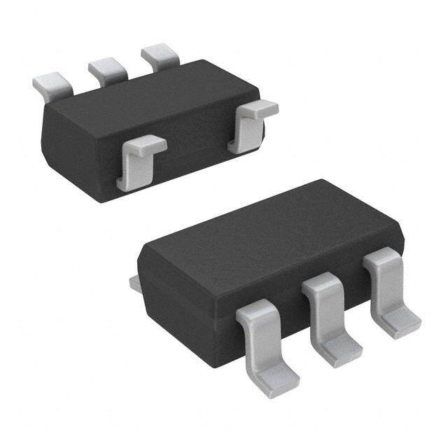
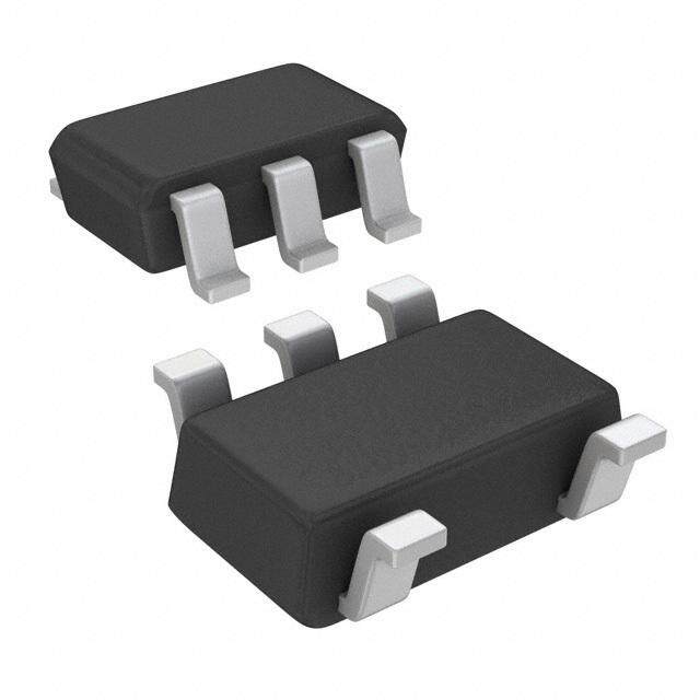
ICGOO电子元器件商城为您提供LP3984IMF-3.1/NOPB由Texas Instruments设计生产,在icgoo商城现货销售,并且可以通过原厂、代理商等渠道进行代购。 LP3984IMF-3.1/NOPB价格参考。Texas InstrumentsLP3984IMF-3.1/NOPB封装/规格:PMIC - 稳压器 - 线性, Linear Voltage Regulator IC Positive Fixed 1 Output 3.1V 150mA SOT-23-5。您可以下载LP3984IMF-3.1/NOPB参考资料、Datasheet数据手册功能说明书,资料中有LP3984IMF-3.1/NOPB 详细功能的应用电路图电压和使用方法及教程。
LP3984IMF-3.1/NOPB 是由 Texas Instruments(德州仪器)生产的一款线性稳压器,属于 PMIC(电源管理集成电路)系列。该器件具有低功耗、高精度和小封装的特点,广泛应用于便携式设备和其他对电源效率和稳定性要求较高的场景。以下是其主要应用场景:

 1. 便携式电子设备
   - LP3984IMF-3.1/NOPB 的低静态电流和高输出电压精度使其非常适合用于电池供电的便携式设备,例如:
     - 智能手机和平板电脑
     - 可穿戴设备(如智能手表、健康监测器)
     - 便携式音频设备(如蓝牙耳机、MP3 播放器)

 2. 通信设备
   - 在通信领域,该稳压器可用于为低功耗射频模块和信号处理单元供电,例如:
     - GSM/CDMA 模块
     - 蓝牙和 Wi-Fi 模块
     - 工业无线传感器网络

 3. 消费类电子产品
   - 该器件的小型封装(MF 封装)和高效性能适合用于各种消费类电子产品,例如:
     - 数码相机和摄像机
     - 遥控器和智能家居控制器
     - 游戏手柄和便携式游戏设备

 4. 工业控制与自动化
   - 在工业应用中,LP3984IMF-3.1/NOPB 可以为微控制器、传感器和其他低功耗组件提供稳定的电源支持,例如:
     - 数据采集系统
     - 工业 PLC(可编程逻辑控制器)
     - 电机驱动器中的辅助电路

 5. 医疗设备
   - 对于需要高精度和低噪声电源的医疗设备,该稳压器可以满足需求,例如:
     - 血压计和血糖仪
     - 便携式心率监测器
     - 医疗传感器和诊断设备

 6. 汽车电子
   - 在汽车应用中,该器件可用于为车载信息娱乐系统或传感器模块供电,例如:
     - 车载导航系统
     - 车内环境监控传感器
     - 低功耗报警系统

 特性总结:
- 输出电压:3.1V(固定)
- 输入电压范围:2.7V 至 5.5V
- 最大输出电流:300mA
- 低静态电流:典型值为 65μA
- 高 PSRR(电源抑制比),适用于低噪声应用
- 小型封装:节省 PCB 空间

综上所述,LP3984IMF-3.1/NOPB 适用于需要高效、稳定和低功耗电源解决方案的各种场景,特别适合电池供电和对空间有严格要求的应用。
| 参数 | 数值 |
| 产品目录 | 集成电路 (IC)半导体 |
| 描述 | IC REG LDO 3.1V 0.15A SOT23-5低压差稳压器 MicroPwr 150mA Ultra LDO CMOS Vtg Reg |
| 产品分类 | |
| 品牌 | Texas Instruments |
| 产品手册 | |
| 产品图片 |
|
| rohs | 符合RoHS无铅 / 符合限制有害物质指令(RoHS)规范要求 |
| 产品系列 | 电源管理 IC,低压差稳压器,Texas Instruments LP3984IMF-3.1/NOPB- |
| 数据手册 | |
| 产品型号 | LP3984IMF-3.1/NOPB |
| PCN设计/规格 | |
| PSRR/纹波抑制—典型值 | 60 dB |
| 产品 | Mircopower Ultra Low-Dropout CMOS Voltage Regulator |
| 产品目录页面 | |
| 产品种类 | 低压差稳压器 |
| 供应商器件封装 | SOT-23-5 |
| 其它名称 | LP3984IMF-3.1/NOPBDKR |
| 包装 | Digi-Reel® |
| 商标 | Texas Instruments |
| 回动电压—最大值 | 120 mV |
| 安装类型 | 表面贴装 |
| 安装风格 | SMD/SMT |
| 封装 | Reel |
| 封装/外壳 | SC-74A,SOT-753 |
| 封装/箱体 | SOT-23-5 |
| 工作温度 | -40°C ~ 125°C |
| 工厂包装数量 | 1000 |
| 最大功率耗散 | 364 mW |
| 最大工作温度 | + 125 C |
| 最大输入电压 | 6 V |
| 最小工作温度 | - 40 C |
| 最小输入电压 | 2.5 V |
| 标准包装 | 1 |
| 电压-跌落(典型值) | 0.075V @ 150mA |
| 电压-输入 | 最高 6V |
| 电压-输出 | 3.1V |
| 电流-输出 | 150mA |
| 电流-限制(最小值) | 300mA |
| 稳压器拓扑 | 正,固定式 |
| 稳压器数 | 1 |
| 类型 | Low dropout low quiescent current regulator |
| 系列 | LP3984 |
| 线路调整率 | 0.05 % |
| 设计资源 | http://www.digikey.com/product-highlights/cn/zh/texas-instruments-webench-design-center/3176 |
| 负载调节 | 0.002 % |
| 输出电压 | 3.1 V |
| 输出电压容差 | +/- 2 % |
| 输出电流 | 150 mA |
| 输出端数量 | 1 Output |
| 输出类型 | Fixed |


- 商务部:美国ITC正式对集成电路等产品启动337调查
- 曝三星4nm工艺存在良率问题 高通将骁龙8 Gen1或转产台积电
- 太阳诱电将投资9.5亿元在常州建新厂生产MLCC 预计2023年完工
- 英特尔发布欧洲新工厂建设计划 深化IDM 2.0 战略
- 台积电先进制程称霸业界 有大客户加持明年业绩稳了
- 达到5530亿美元!SIA预计今年全球半导体销售额将创下新高
- 英特尔拟将自动驾驶子公司Mobileye上市 估值或超500亿美元
- 三星加码芯片和SET,合并消费电子和移动部门,撤换高东真等 CEO
- 三星电子宣布重大人事变动 还合并消费电子和移动部门
- 海关总署:前11个月进口集成电路产品价值2.52万亿元 增长14.8%


PDF Datasheet 数据手册内容提取
LP3984 www.ti.com SNVS160F–OCTOBER2001–REVISEDOCTOBER2013 LP3984 Micropower 150 mA Ultra Low-Dropout CMOS Voltage Regulator in Subminiature 4-I/O DSBGA Package CheckforSamples:LP3984 FEATURES DESCRIPTION 1 • Miniature4-I/ODSBGAorSOT-23-5Package The LP3984 is designed for portable and wireless 2 applications with demanding performance and space • Logiccontrolledenable requirements. • StablewithTantalumCapacitors The LP3984's performance is optimized for battery • 1µFTantalumOutputCapacitor powered systems to deliver extremely low dropout • FastTurn-On voltage and low quiescent current. Regulator ground • ThermalShutdownandShort-CircuitCurrent current increases only slightly in dropout, further prolongingthebatterylife. Limit Power supply rejection is better than 60 dB at low KEY SPECIFICATIONS frequencies and starts to roll off at 10 kHz. High power supply rejection is maintained down to low • 2.5to6.0VInputRange input voltage levels common to battery operated • 150mAOutput circuits. • 60dBPSRRat1kHz,40dBat10kHz@3.1V IN The device is ideal for mobile phone and similar • ≤1.2 µAQuiescentCurrentwhenShutDown battery powered wireless applications. It provides up • FastTurn-OnTime:20µs(typ.) to 150 mA from a 2.5V to 6V input. The LP3984 consumes less than 1.2 µA in disable mode and has • 75mVtypDropoutwith150mALoad fastturn-ontimelessthan20µs. • −40to+125°CJunctionTemperatureRangefor The LP3984 is available in a 4-bump DSBGA and 5- Operation pin SOT-23 packages. Performance is specified for • 1.5V,1.8V,2.9Vand3.1V −40°C to +125°C temperature range and is available in 1.5V, 1.8V, 2.9V and 3.1V output voltages. For APPLICATIONS other output voltage options from 1.5V to 3.5V, • CDMACellularHandsets pleasecontactTIsalesoffice. • WidebandCDMACellularHandsets • GSMCellularHandsets • PortableInformationAppliances Typical Application Circuit 1(B2) 5(B1) VIN VOUT 1PF LP3984 1PF Tant 3(A2) 4 VEN NC 2(A1) Note:PinNumbersinparenthesisindicateDSBGApackage. 1 Pleasebeawarethatanimportantnoticeconcerningavailability,standardwarranty,anduseincriticalapplicationsof TexasInstrumentssemiconductorproductsanddisclaimerstheretoappearsattheendofthisdatasheet. Alltrademarksarethepropertyoftheirrespectiveowners. 2 PRODUCTIONDATAinformationiscurrentasofpublicationdate. Copyright©2001–2013,TexasInstrumentsIncorporated Products conform to specifications per the terms of the Texas Instruments standard warranty. Production processing does not necessarilyincludetestingofallparameters.
LP3984 SNVS160F–OCTOBER2001–REVISEDOCTOBER2013 www.ti.com Block Diagram PinDescriptions Name DSBGA (1) SOT Function V A2 3 EnableInputLogic,EnableHigh EN GND A1 2 CommonGround V B1 5 OutputVoltageoftheLDO OUT V B2 1 InputVoltageoftheLDO IN N.C. 4 NoConnection (1) ThepinnumberingschemefortheDSBGApackagewasrevisedinApril2002toconformtoJEDECstandards.Onlythepinnumbers wererevised.Nochangestothephysicallocationsoftheinputs/outputsweremade.Forreferencepurposes,theobsoletenumbering schemehadGNDaspin1,V aspin2,V aspin3andV aspin4. OUT IN EN Connection Diagram SOT-23-5Package Figure1. TopView SeePackageNumberDBV DSBGA,4-BumpPackage Figure2. TopView SeePackageNumberYPB0004 2 SubmitDocumentationFeedback Copyright©2001–2013,TexasInstrumentsIncorporated ProductFolderLinks:LP3984
LP3984 www.ti.com SNVS160F–OCTOBER2001–REVISEDOCTOBER2013 Thesedeviceshavelimitedbuilt-inESDprotection.Theleadsshouldbeshortedtogetherorthedeviceplacedinconductivefoam duringstorageorhandlingtopreventelectrostaticdamagetotheMOSgates. ABSOLUTE MAXIMUM RATINGS(1)(2)(3) V ,V −0.3to6.5V IN EN V –0.3to(V +0.3)≤6.5V OUT IN JunctionTemperature 150°C StorageTemperature −65°Cto+150°C LeadTemp. 235°C PadTemp.(4) 235°C MaximumPowerDissipation(5) SOT-23-5 364mW DSBGA 235mW ESDRating(6) HumanBodyModel 2kV MachineModel 200V (1) Stressesbeyondthoselistedunderabsolutemaximumratingsmaycausepermanentdamagetothedevice.Thesearestressratings only,andfunctionaloperationofthedeviceattheseoranyotherconditionsbeyondthoseindicatedunderrecommendedoperating conditionsisnotimplied.Exposuretoabsolute-maximum-ratedconditionsforextendedperiodsmayaffectdevicereliability. (2) AllvoltagesarewithrespecttothepotentialattheGNDpin. (3) IfMilitary/Aerospacespecifieddevicesarerequired,pleasecontacttheTexasInstrumentsSalesOffice/Distributorsforavailabilityand specifications. (4) AdditionalinformationonpadtemperaturecanbefoundintheTIAN-1112ApplicationReport(). (5) TheAbsoluteMaximumpowerdissipationdependsontheambienttemperatureandcanbecalculatedusingtheformula:P =(T - D J T )/θ ,whereT isthejunctiontemperature,T istheambienttemperature,andθ isthejunction-to-ambientthermalresistance.The A JA J A JA 364mWratingforSOT23-5appearingunderAbsoluteMaximumRatingsresultsfromsubstitutingtheAbsoluteMaximumjunction temperature,150°C,forT,70°CforT ,and220°C/Wforθ .Morepowercanbedissipatedsafelyatambienttemperaturesbelow J A JA 70°C.Lesspowercanbedissipatedsafelyatambienttemperaturesabove70°C.TheAbsoluteMaximumpowerdissipationforSOT23- 5canbeincreasedby4.5mWforeachdegreebelow70°C,anditmustbederatedby4.5mWforeachdegreeabove70°C. (6) Thehumanbodymodelis100pFdischargedthrough1.5kΩresistorintoeachpin.Themachinemodelisa200pFcapacitordischarged directlyintoeachpin. OPERATING RATINGS(1)(2) V 2.5to6V IN V 0to(V +0.3V)≤6V EN IN JunctionTemperature −40°Cto+125°C ThermalResistance θ (SOT23-5) 220°C/W JA θ (DSBGA) 340°C/W JA MaximumPowerDissipation(3) SOT-23-5 250mW DSBGA 160mW (1) Stressesbeyondthoselistedunderabsolutemaximumratingsmaycausepermanentdamagetothedevice.Thesearestressratings only,andfunctionaloperationofthedeviceattheseoranyotherconditionsbeyondthoseindicatedunderrecommendedoperating conditionsisnotimplied.Exposuretoabsolute-maximum-ratedconditionsforextendedperiodsmayaffectdevicereliability. (2) AllvoltagesarewithrespecttothepotentialattheGNDpin. (3) LiketheAbsoluteMaximumpowerdissipation,themaximumpowerdissipationforoperationdependsontheambienttemperature.The 250mWratingforSOT23-5appearingunderOperatingRatingsresultsfromsubstitutingthemaximumjunctiontemperaturefor operation,125°C,forT,70°CforT ,and220°C/Wforθ usingtheformula:P =(T -T )/θ .Morepowercanbedissipatedat J A JA D J A JA ambienttemperaturesbelow70°C.Lesspowercanbedissipatedatambienttemperaturesabove70°C.Themaximumpower dissipationforoperationcanbeincreasedby4.5mWforeachdegreebelow70°C,anditmustbederatedby4.5mWforeachdegree above70°C. Copyright©2001–2013,TexasInstrumentsIncorporated SubmitDocumentationFeedback 3 ProductFolderLinks:LP3984
LP3984 SNVS160F–OCTOBER2001–REVISEDOCTOBER2013 www.ti.com ELECTRICAL CHARACTERISTICS Unlessotherwisespecified:V =2.5Vfor1.5Vand1.8Voptions,V =V +0.5foroutputoptionshigherthan2.5V,C =1 IN IN OUT IN µF,I =1mA,C =1µF,tantalum.TypicalvaluesandlimitsappearinginstandardtypefaceareforT =25°C.Limits OUT OUT J appearinginboldfacetypeapplyovertheentirejunctiontemperaturerangeforoperation,−40°Cto+125°C. (1) (2) Limit Symbol Parameter Conditions Typ Units Min Max OutputVoltageTolerance −1.2 1.2 %of −2.0 2.0 V OUT(nom) LineRegulationError V =2.5Vto4.5Vfor1.5Vand1.8V IN options 0.05 −0.15 0.15 %/V ΔVOUT VIN=(VOUT+0.5V)to4.5VforVoltage optionshigherthan2.5V LoadRegulationError(3) I =1mAto150mA OUT 0.002 0.005 LP3984IM5(SOT-23-5) %/mA LP3984IBP(DSBGA) 0.0009 0.002 V =V +0.2V, IN OUT(nom) f=1kHz, 60 I =50mA,Figure4 OUT PSRR PowerSupplyRejectionRatio dB V =V +0.2V, IN OUT(nom) f=10kHz, 40 I =50mA,Figure4 OUT I QuiescentCurrent V =1.4V,I =0mA 80 125 Q EN OUT V =1.4V,I =0to150mA 110 150 µA EN OUT V =0.4V 0.005 1.2 EN DropoutVoltage(4) I =1mA 0.6 2.5 OUT I =50mA 25 40 OUT mV I =100mA 50 80 OUT I =150mA 75 120 OUT I ShortCircuitCurrentLimit OutputGrounded SC 600 mA (SteadyState) I PeakOutputCurrent V ≥V -5% 600 300 mA OUT(PK) OUT OUT(nom) T Turn-OnTime(5) 20 µs ON e OutputNoiseVoltage BW=10Hzto100kHz, n 90 µVrms C =1µFtant. OUT I MaximumInputCurrentatEN V =0.4andV =6.0 ±1 nA EN EN IN V MaximumLowLevelInputVoltage V =2.5to6.0V IL IN 0.4 V atEN V MinimumHighLevelInputVoltage V =2.5to6.0V IH IN 1.4 V atEN C OutputCapacitor Capacitance 1 22 µF OUT ESR 2 10 Ω ThermalShutdownTemperature 160 °C TSD ThermalShutdownHysteresis 20 °C (1) MinandMaxLimitsareverifiedbydesign,test,orstatisticalanalysis.Typical(Typ.)numbersarenotverified,butdorepresentthemost likelynorm. (2) Thetargetoutputvoltage,whichislabeledV ,isthedesiredvoltageoption. OUT(nom) (3) Anincreaseintheloadcurrentresultsinaslightdecreaseintheoutputvoltageandviceversa. (4) Dropoutvoltageistheinput-to-outputvoltagedifferenceatwhichtheoutputvoltageis100mVbelowitsnominalvalue.This specificationdoesnotapplyforinputvoltagesbelow2.5V. (5) Turn-ontimeistimemeasuredbetweentheenableinputjustexceedingV andtheoutputvoltagejustreaching95%ofitsnominal IH value. 4 SubmitDocumentationFeedback Copyright©2001–2013,TexasInstrumentsIncorporated ProductFolderLinks:LP3984
LP3984 www.ti.com SNVS160F–OCTOBER2001–REVISEDOCTOBER2013 Figure3. LineTransientInputTestSignal Figure4. PSRRInputTestSignal Copyright©2001–2013,TexasInstrumentsIncorporated SubmitDocumentationFeedback 5 ProductFolderLinks:LP3984
LP3984 SNVS160F–OCTOBER2001–REVISEDOCTOBER2013 www.ti.com TYPICAL PERFORMANCE CHARACTERISTICS Unlessotherwisespecified,C =C =1µFTantalum,V =2.5for1.5Vand1.8Voptions,V =V +0.2Vforoutput IN OUT IN IN OUT optionshigherthan2.5V,T =25°C,EnablepinistiedtoV . A IN PowerSupplyRejectionRatio(V =3.5V) PowerSupplyRejectionRatio(V =3.5V) IN IN Figure5. Figure6. PowerSupplyRejectionRatio(V =3.5V) PowerSupplyRejectionRatio(LP3984-1.5,V =2.5V) IN IN Figure7. Figure8. LineTransientResponse(LP3984-3.1) LineTransientResponse(LP3984-3.1) Figure9. Figure10. 6 SubmitDocumentationFeedback Copyright©2001–2013,TexasInstrumentsIncorporated ProductFolderLinks:LP3984
LP3984 www.ti.com SNVS160F–OCTOBER2001–REVISEDOCTOBER2013 TYPICAL PERFORMANCE CHARACTERISTICS (continued) Unlessotherwisespecified,C =C =1µFTantalum,V =2.5for1.5Vand1.8Voptions,V =V +0.2Vforoutput IN OUT IN IN OUT optionshigherthan2.5V,T =25°C,EnablepinistiedtoV . A IN LineTransientResponse(LP3984-3.1) LineTransientResponse(LP3984-3.1) Figure11. Figure12. LineTransientResponse(LP3984-3.1) LineTransientResponse(LP3984-3.1) Figure13. Figure14. StartUpResponse StartUpResponse Figure15. Figure16. Copyright©2001–2013,TexasInstrumentsIncorporated SubmitDocumentationFeedback 7 ProductFolderLinks:LP3984
LP3984 SNVS160F–OCTOBER2001–REVISEDOCTOBER2013 www.ti.com TYPICAL PERFORMANCE CHARACTERISTICS (continued) Unlessotherwisespecified,C =C =1µFTantalum,V =2.5for1.5Vand1.8Voptions,V =V +0.2Vforoutput IN OUT IN IN OUT optionshigherthan2.5V,T =25°C,EnablepinistiedtoV . A IN EnableResponse LoadTransientResponse(LP3984-3.1 Figure17. Figure18. LoadTransientResponse(LP3984-3.1) LoadTransientResponse(V =4.2V) IN Figure19. Figure20. 8 SubmitDocumentationFeedback Copyright©2001–2013,TexasInstrumentsIncorporated ProductFolderLinks:LP3984
LP3984 www.ti.com SNVS160F–OCTOBER2001–REVISEDOCTOBER2013 APPLICATION HINTS External Capacitors Like any low-dropout regulator, the LP3984 requires external capacitors for regulator stability. The LP3984 is specifically designed for portable applications requiring minimum board space and smallest components. These capacitorsmustbecorrectlyselectedforgoodperformance. Input Capacitors An input capacitance of ≊ 1 µF is required between the LP3984 input pin and ground (the amount of the capacitancemaybeincreasedwithoutlimit). This capacitor must be located a distance of not more than 1 cm from the input pin and returned to a clean analogground.Anygoodqualityceramic,tantalum,orfilmcapacitormaybeusedattheinput. Important: Tantalum capacitors can suffer catastrophic failures due to surge current when connected to a low- impedance source of power (like a battery or a very large capacitor). If a tantalum capacitor is used at the input, itmustbespecifiedbythemanufacturertohaveasurgecurrentratingsufficientfortheapplication. There are no requirements for the ESR on the input capacitor, but tolerance and temperature coefficient must be considered when selecting the capacitor to ensure the capacitance will be ≊ 1 µF over the entire operating temperaturerange. Output Capacitor The LP3984 is designed specifically to work with tantalum output capacitors. A tantalum capacitor in 1 to 22 µF rangewith2Ωto10Ω ESRrangeissuitableintheLP3984applicationcircuit. Itmayalsobepossibletousefilmcapacitorsattheoutput,butthesearenotasattractiveforreasonsofsizeand cost. The output capacitor must meet the requirement for minimum amount of capacitance and also have an ESR (EquivalentSeriesResistance)valuewhichiswithinastablerange(2Ω to10Ω). No-Load Stability The LP3984 will remain stable and in regulation with no external load. This is specially important in CMOS RAM keep-aliveapplications. On/Off Input Operation The LP3984 is turned off by pulling the V pin low, and turned on by pulling it high. If this feature is not used, EN the V pin should be tied to V to keep the regulator output on at all times. To assure proper operation, the EN IN signalsourceusedtodrivetheV inputmustbeabletoswingaboveandbelowthespecifiedturn-on/offvoltage EN thresholdslistedintheElectricalCharacteristicssectionunderV andV . IL IH Fast On-Time The LP3984 output is turned on after V voltage reaches its final value (1.23V nominal). To speed up this ref process, the noise reduction capacitor at the bypass pin is charged with an internal 70 µA current source. The current source is turned off when the bandgap voltage reaches approximately 95% of its final value. The turn-on time is determined by the time constant of the bypass capacitor. The smaller the capacitor value, the shorter the turn-on time, but less noise gets reduced. As a result, turn-on time and noise reduction need to be taken into designconsiderationwhenchoosingthevalueofthebypasscapacitor. Copyright©2001–2013,TexasInstrumentsIncorporated SubmitDocumentationFeedback 9 ProductFolderLinks:LP3984
LP3984 SNVS160F–OCTOBER2001–REVISEDOCTOBER2013 www.ti.com DSBGA Mounting The DSBGA package requires specific mounting techniques which are detailed in the AN-1112 Application Report (SNVA009). Referring to the section PCB Layout ; note that the pad style which must be used with the 5- pinpackageisNSMD(non-soldermaskdefined)type. For best results during assembly, alignment ordinals on the PC board may be used to facilitate placement of the DSBGAdevice. DSBGA Light Sensitivity Exposing the DSBGA device to direct sunlight will cause mis-operation of the device. Light sources such as halogenlampscanaffectelectricalperformanceifbroughtneartothedevice. The wavelengths which have most detrimental effect are reds and infra-reds, which means that the fluorescent lighting used inside most buildings has very little effect on performance. A DSBGA test board was brought to within 1 cm of a fluorescent desk lamp and the effect on the regulated output voltage was negligible, showing a deviationoflessthan0.1%fromnominal. 10 SubmitDocumentationFeedback Copyright©2001–2013,TexasInstrumentsIncorporated ProductFolderLinks:LP3984
LP3984 www.ti.com SNVS160F–OCTOBER2001–REVISEDOCTOBER2013 REVISION HISTORY ChangesfromRevisionD(May2013)toRevisionE Page • ChangedlayoutofNationalDataSheettoTIformat;correcttypos ................................................................................... 10 ChangesfromRevisionE(May2013)toRevisionF Page • Deleted2.0Voptionwhichisobsoleted................................................................................................................................ 1 • Deletedlegacyorderingtable ............................................................................................................................................... 3 Copyright©2001–2013,TexasInstrumentsIncorporated SubmitDocumentationFeedback 11 ProductFolderLinks:LP3984
PACKAGE OPTION ADDENDUM www.ti.com 17-Aug-2016 PACKAGING INFORMATION Orderable Device Status Package Type Package Pins Package Eco Plan Lead/Ball Finish MSL Peak Temp Op Temp (°C) Device Marking Samples (1) Drawing Qty (2) (6) (3) (4/5) LP3984IMF-1.5 LIFEBUY SOT-23 DBV 5 1000 TBD Call TI Call TI LEAB LP3984IMF-1.5/NOPB LIFEBUY SOT-23 DBV 5 1000 Green (RoHS CU SN Level-1-260C-UNLIM LEAB & no Sb/Br) LP3984IMF-1.8 LIFEBUY SOT-23 DBV 5 1000 TBD Call TI Call TI LEBB LP3984IMF-1.8/NOPB LIFEBUY SOT-23 DBV 5 1000 Green (RoHS CU SN Level-1-260C-UNLIM LEBB & no Sb/Br) LP3984IMF-3.1/NOPB LIFEBUY SOT-23 DBV 5 1000 Green (RoHS CU SN Level-1-260C-UNLIM -40 to 125 LEDB & no Sb/Br) LP3984IMFX-1.8 NRND SOT-23 DBV 5 TBD Call TI Call TI -40 to 125 LEBB LP3984IMFX-1.8/NOPB LIFEBUY SOT-23 DBV 5 3000 Green (RoHS CU SN Level-1-260C-UNLIM -40 to 125 LEBB & no Sb/Br) LP3984ITP-2.9/NOPB LIFEBUY DSBGA YPB 4 250 Green (RoHS SNAGCU Level-1-260C-UNLIM -40 to 125 & no Sb/Br) LP3984ITPX-1.8/NOPB LIFEBUY DSBGA YPB 4 3000 Green (RoHS SNAGCU Level-1-260C-UNLIM -40 to 125 & no Sb/Br) (1) The marketing status values are defined as follows: ACTIVE: Product device recommended for new designs. LIFEBUY: TI has announced that the device will be discontinued, and a lifetime-buy period is in effect. NRND: Not recommended for new designs. Device is in production to support existing customers, but TI does not recommend using this part in a new design. PREVIEW: Device has been announced but is not in production. Samples may or may not be available. OBSOLETE: TI has discontinued the production of the device. (2) Eco Plan - The planned eco-friendly classification: Pb-Free (RoHS), Pb-Free (RoHS Exempt), or Green (RoHS & no Sb/Br) - please check http://www.ti.com/productcontent for the latest availability information and additional product content details. TBD: The Pb-Free/Green conversion plan has not been defined. Pb-Free (RoHS): TI's terms "Lead-Free" or "Pb-Free" mean semiconductor products that are compatible with the current RoHS requirements for all 6 substances, including the requirement that lead not exceed 0.1% by weight in homogeneous materials. Where designed to be soldered at high temperatures, TI Pb-Free products are suitable for use in specified lead-free processes. Pb-Free (RoHS Exempt): This component has a RoHS exemption for either 1) lead-based flip-chip solder bumps used between the die and package, or 2) lead-based die adhesive used between the die and leadframe. The component is otherwise considered Pb-Free (RoHS compatible) as defined above. Green (RoHS & no Sb/Br): TI defines "Green" to mean Pb-Free (RoHS compatible), and free of Bromine (Br) and Antimony (Sb) based flame retardants (Br or Sb do not exceed 0.1% by weight in homogeneous material) (3) MSL, Peak Temp. - The Moisture Sensitivity Level rating according to the JEDEC industry standard classifications, and peak solder temperature. (4) There may be additional marking, which relates to the logo, the lot trace code information, or the environmental category on the device. Addendum-Page 1
PACKAGE OPTION ADDENDUM www.ti.com 17-Aug-2016 (5) Multiple Device Markings will be inside parentheses. Only one Device Marking contained in parentheses and separated by a "~" will appear on a device. If a line is indented then it is a continuation of the previous line and the two combined represent the entire Device Marking for that device. (6) Lead/Ball Finish - Orderable Devices may have multiple material finish options. Finish options are separated by a vertical ruled line. Lead/Ball Finish values may wrap to two lines if the finish value exceeds the maximum column width. Important Information and Disclaimer:The information provided on this page represents TI's knowledge and belief as of the date that it is provided. TI bases its knowledge and belief on information provided by third parties, and makes no representation or warranty as to the accuracy of such information. Efforts are underway to better integrate information from third parties. TI has taken and continues to take reasonable steps to provide representative and accurate information but may not have conducted destructive testing or chemical analysis on incoming materials and chemicals. TI and TI suppliers consider certain information to be proprietary, and thus CAS numbers and other limited information may not be available for release. In no event shall TI's liability arising out of such information exceed the total purchase price of the TI part(s) at issue in this document sold by TI to Customer on an annual basis. Addendum-Page 2
PACKAGE MATERIALS INFORMATION www.ti.com 20-Dec-2016 TAPE AND REEL INFORMATION *Alldimensionsarenominal Device Package Package Pins SPQ Reel Reel A0 B0 K0 P1 W Pin1 Type Drawing Diameter Width (mm) (mm) (mm) (mm) (mm) Quadrant (mm) W1(mm) LP3984IMF-1.5 SOT-23 DBV 5 1000 178.0 8.4 3.2 3.2 1.4 4.0 8.0 Q3 LP3984IMF-1.5/NOPB SOT-23 DBV 5 1000 178.0 8.4 3.2 3.2 1.4 4.0 8.0 Q3 LP3984IMF-1.8 SOT-23 DBV 5 1000 178.0 8.4 3.2 3.2 1.4 4.0 8.0 Q3 LP3984IMF-1.8/NOPB SOT-23 DBV 5 1000 178.0 8.4 3.2 3.2 1.4 4.0 8.0 Q3 LP3984IMF-3.1/NOPB SOT-23 DBV 5 1000 178.0 8.4 3.2 3.2 1.4 4.0 8.0 Q3 LP3984IMFX-1.8/NOPB SOT-23 DBV 5 3000 178.0 8.4 3.2 3.2 1.4 4.0 8.0 Q3 LP3984ITP-2.9/NOPB DSBGA YPB 4 250 178.0 8.4 1.02 1.09 0.66 4.0 8.0 Q1 LP3984ITPX-1.8/NOPB DSBGA YPB 4 3000 178.0 8.4 1.02 1.09 0.66 4.0 8.0 Q1 PackMaterials-Page1
PACKAGE MATERIALS INFORMATION www.ti.com 20-Dec-2016 *Alldimensionsarenominal Device PackageType PackageDrawing Pins SPQ Length(mm) Width(mm) Height(mm) LP3984IMF-1.5 SOT-23 DBV 5 1000 210.0 185.0 35.0 LP3984IMF-1.5/NOPB SOT-23 DBV 5 1000 210.0 185.0 35.0 LP3984IMF-1.8 SOT-23 DBV 5 1000 210.0 185.0 35.0 LP3984IMF-1.8/NOPB SOT-23 DBV 5 1000 210.0 185.0 35.0 LP3984IMF-3.1/NOPB SOT-23 DBV 5 1000 210.0 185.0 35.0 LP3984IMFX-1.8/NOPB SOT-23 DBV 5 3000 210.0 185.0 35.0 LP3984ITP-2.9/NOPB DSBGA YPB 4 250 210.0 185.0 35.0 LP3984ITPX-1.8/NOPB DSBGA YPB 4 3000 210.0 185.0 35.0 PackMaterials-Page2
None
None
PACKAGE OUTLINE YPB0004 DSBGA - 0.575 mm max height SCALE 12.000 DIE SIZE BALL GRID ARRAY B E A BALL A1 CORNER D 0.575 MAX C SEATING PLANE 0.15 BALL TYP 0.11 0.05 C 0.5 B SYMM 0.5 D: Max = 1.019 mm, Min =0 .958 mm E: Max = 0.905 mm, Min =0 .844 mm A 1 2 0.18 SYMM 4X 0.16 0.015 C A B 4215097/B 07/2016 NOTES: 1. All linear dimensions are in millimeters. Any dimensions in parenthesis are for reference only. Dimensioning and tolerancing per ASME Y14.5M. 2. This drawing is subject to change without notice. www.ti.com
EXAMPLE BOARD LAYOUT YPB0004 DSBGA - 0.575 mm max height DIE SIZE BALL GRID ARRAY (0.5) 4X ( 0.16) 1 2 A SYMM (0.5) B SYMM LAND PATTERN EXAMPLE SCALE:40X ( 0.16) 0.05 MAX METAL UNDER 0.05 MIN METAL SOLDER MASK SOLDER MASK ( 0.16) OPENING SOLDER MASK OPENING NON-SOLDER MASK DEFINED SOLDER MASK (PREFERRED) DEFINED SOLDER MASK DETAILS NOT TO SCALE 4215097/B 07/2016 NOTES: (continued) 3. Final dimensions may vary due to manufacturing tolerance considerations and also routing constraints. See Texas Instruments Literature No. SNVA009 (www.ti.com/lit/snva009). www.ti.com
EXAMPLE STENCIL DESIGN YPB0004 DSBGA - 0.575 mm max height DIE SIZE BALL GRID ARRAY (0.5) TYP 4X ( 0.3) (R0.05) TYP 1 2 A SYMM (0.5) TYP B METAL TYP SYMM SOLDER PASTE EXAMPLE BASED ON 0.125mm THICK STENCIL SCALE:50X 4215097/B 07/2016 NOTES: (continued) 4. Laser cutting apertures with trapezoidal walls and rounded corners may offer better paste release. www.ti.com
IMPORTANTNOTICEFORTIDESIGNINFORMATIONANDRESOURCES TexasInstrumentsIncorporated(‘TI”)technical,applicationorotherdesignadvice,servicesorinformation,including,butnotlimitedto, referencedesignsandmaterialsrelatingtoevaluationmodules,(collectively,“TIResources”)areintendedtoassistdesignerswhoare developingapplicationsthatincorporateTIproducts;bydownloading,accessingorusinganyparticularTIResourceinanyway,you (individuallyor,ifyouareactingonbehalfofacompany,yourcompany)agreetouseitsolelyforthispurposeandsubjecttothetermsof thisNotice. TI’sprovisionofTIResourcesdoesnotexpandorotherwisealterTI’sapplicablepublishedwarrantiesorwarrantydisclaimersforTI products,andnoadditionalobligationsorliabilitiesarisefromTIprovidingsuchTIResources.TIreservestherighttomakecorrections, enhancements,improvementsandotherchangestoitsTIResources. Youunderstandandagreethatyouremainresponsibleforusingyourindependentanalysis,evaluationandjudgmentindesigningyour applicationsandthatyouhavefullandexclusiveresponsibilitytoassurethesafetyofyourapplicationsandcomplianceofyourapplications (andofallTIproductsusedinorforyourapplications)withallapplicableregulations,lawsandotherapplicablerequirements.You representthat,withrespecttoyourapplications,youhaveallthenecessaryexpertisetocreateandimplementsafeguardsthat(1) anticipatedangerousconsequencesoffailures,(2)monitorfailuresandtheirconsequences,and(3)lessenthelikelihoodoffailuresthat mightcauseharmandtakeappropriateactions.YouagreethatpriortousingordistributinganyapplicationsthatincludeTIproducts,you willthoroughlytestsuchapplicationsandthefunctionalityofsuchTIproductsasusedinsuchapplications.TIhasnotconductedany testingotherthanthatspecificallydescribedinthepublisheddocumentationforaparticularTIResource. Youareauthorizedtouse,copyandmodifyanyindividualTIResourceonlyinconnectionwiththedevelopmentofapplicationsthatinclude theTIproduct(s)identifiedinsuchTIResource.NOOTHERLICENSE,EXPRESSORIMPLIED,BYESTOPPELOROTHERWISETO ANYOTHERTIINTELLECTUALPROPERTYRIGHT,ANDNOLICENSETOANYTECHNOLOGYORINTELLECTUALPROPERTY RIGHTOFTIORANYTHIRDPARTYISGRANTEDHEREIN,includingbutnotlimitedtoanypatentright,copyright,maskworkright,or otherintellectualpropertyrightrelatingtoanycombination,machine,orprocessinwhichTIproductsorservicesareused.Information regardingorreferencingthird-partyproductsorservicesdoesnotconstitutealicensetousesuchproductsorservices,orawarrantyor endorsementthereof.UseofTIResourcesmayrequirealicensefromathirdpartyunderthepatentsorotherintellectualpropertyofthe thirdparty,oralicensefromTIunderthepatentsorotherintellectualpropertyofTI. TIRESOURCESAREPROVIDED“ASIS”ANDWITHALLFAULTS.TIDISCLAIMSALLOTHERWARRANTIESOR REPRESENTATIONS,EXPRESSORIMPLIED,REGARDINGTIRESOURCESORUSETHEREOF,INCLUDINGBUTNOTLIMITEDTO ACCURACYORCOMPLETENESS,TITLE,ANYEPIDEMICFAILUREWARRANTYANDANYIMPLIEDWARRANTIESOF MERCHANTABILITY,FITNESSFORAPARTICULARPURPOSE,ANDNON-INFRINGEMENTOFANYTHIRDPARTYINTELLECTUAL PROPERTYRIGHTS. TISHALLNOTBELIABLEFORANDSHALLNOTDEFENDORINDEMNIFYYOUAGAINSTANYCLAIM,INCLUDINGBUTNOT LIMITEDTOANYINFRINGEMENTCLAIMTHATRELATESTOORISBASEDONANYCOMBINATIONOFPRODUCTSEVENIF DESCRIBEDINTIRESOURCESOROTHERWISE.INNOEVENTSHALLTIBELIABLEFORANYACTUAL,DIRECT,SPECIAL, COLLATERAL,INDIRECT,PUNITIVE,INCIDENTAL,CONSEQUENTIALOREXEMPLARYDAMAGESINCONNECTIONWITHOR ARISINGOUTOFTIRESOURCESORUSETHEREOF,ANDREGARDLESSOFWHETHERTIHASBEENADVISEDOFTHE POSSIBILITYOFSUCHDAMAGES. YouagreetofullyindemnifyTIanditsrepresentativesagainstanydamages,costs,losses,and/orliabilitiesarisingoutofyournon- compliancewiththetermsandprovisionsofthisNotice. ThisNoticeappliestoTIResources.Additionaltermsapplytotheuseandpurchaseofcertaintypesofmaterials,TIproductsandservices. Theseinclude;withoutlimitation,TI’sstandardtermsforsemiconductorproductshttp://www.ti.com/sc/docs/stdterms.htm),evaluation modules,andsamples(http://www.ti.com/sc/docs/sampterms.htm). MailingAddress:TexasInstruments,PostOfficeBox655303,Dallas,Texas75265 Copyright©2017,TexasInstrumentsIncorporated

 Datasheet下载


