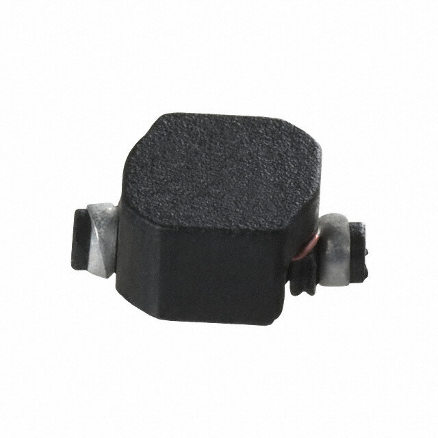
ICGOO在线商城 > LP0402N3500ANTR
- 型号: LP0402N3500ANTR
- 制造商: AVX
- 库位|库存: xxxx|xxxx
- 要求:
| 数量阶梯 | 香港交货 | 国内含税 |
| +xxxx | $xxxx | ¥xxxx |
查看当月历史价格
查看今年历史价格
LP0402N3500ANTR产品简介:
ICGOO电子元器件商城为您提供LP0402N3500ANTR由AVX设计生产,在icgoo商城现货销售,并且可以通过原厂、代理商等渠道进行代购。 提供LP0402N3500ANTR价格参考以及AVXLP0402N3500ANTR封装/规格参数等产品信息。 你可以下载LP0402N3500ANTR参考资料、Datasheet数据手册功能说明书, 资料中有LP0402N3500ANTR详细功能的应用电路图电压和使用方法及教程。
| 参数 | 数值 |
| 品牌 | AVX |
| 产品目录 | 无源元件 |
| 描述 | 信号调节 Low Pass Filter 3500 MHz |
| 产品分类 | 信号调节 |
| 产品手册 | |
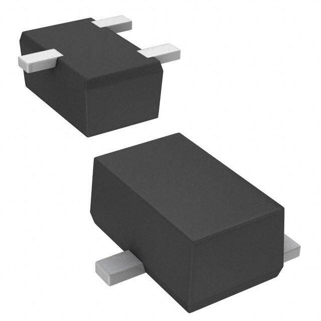
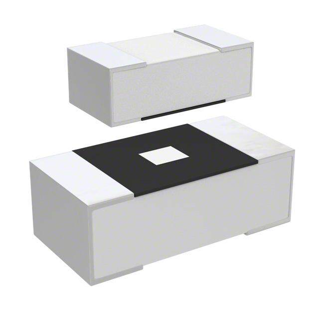
| 产品图片 |
|
| rohs | 符合RoHS |
| 产品系列 | AVX LP0402N3500ANTR |
| 产品型号 | LP0402N3500ANTR |
| 产品 | Low Pass Filters |
| 产品种类 | 信号调节 |
| 商标 | AVX |
| 封装 | Reel |
| 封装/箱体 | 0402 (1005 metric) |
| 工作温度范围 | - 40 C to + 85 C |
| 工厂包装数量 | 5000 |
| 端接类型 | SMD/SMT |
| 频率 | 3500 MHz |
| 频率范围 | 3400 MHz to 3600 MHz |


- 商务部:美国ITC正式对集成电路等产品启动337调查
- 曝三星4nm工艺存在良率问题 高通将骁龙8 Gen1或转产台积电
- 太阳诱电将投资9.5亿元在常州建新厂生产MLCC 预计2023年完工
- 英特尔发布欧洲新工厂建设计划 深化IDM 2.0 战略
- 台积电先进制程称霸业界 有大客户加持明年业绩稳了
- 达到5530亿美元!SIA预计今年全球半导体销售额将创下新高
- 英特尔拟将自动驾驶子公司Mobileye上市 估值或超500亿美元
- 三星加码芯片和SET,合并消费电子和移动部门,撤换高东真等 CEO
- 三星电子宣布重大人事变动 还合并消费电子和移动部门
- 海关总署:前11个月进口集成电路产品价值2.52万亿元 增长14.8%


PDF Datasheet 数据手册内容提取
Thin-Film Low Pass Filter LP0402N Series Harmonic Lead-Free LGA Termination RFAP TECHNOLOGY APPLICATIONS The LP0402N Series Harmonic Low Pass Filter is based on • Wireless communications the proprietary RFAP Thin-Film multilayer technology. The • Wireless LAN’s technology provides a miniature part with excellent high • GPS frequency performance and rugged construction for reliable • WiMAX automatic assembly. The RFAP Harmonic Low Pass Filter is offered in a variety of LAND GRID ARRAY ADVANTAGES frequency bands compatible with various types of high frequency wireless systems. • Inherent Low Profile • Self Alignment during Reflow • Excellent Solderability • Low Parasitics • Better Heat Dissipation HOW TO ORDER LP 0402 N XXXX X N TR Style Size Type Frequency Sub-Type Termination Taped & Reeled MHz LGA Lead Free QUALITY INSPECTION Finished parts are 100% tested for electrical parameters and LEAD-FREE COMPATIBLE visual characteristics. Each production lot is evaluated on a COMPONENT 4 sample basis for: • Static Humidity: 85ºC, 85% RH, 160 hours • Endurance: 125ºC, IR, 4 hours TERMINATION Nickel/Lead-Free solder coating compatible with automatic soldering technologies: reflow, wave soldering, vapor phase and manual. 101
Thin-Film Low Pass Filter LP0402N Series Harmonic Lead-Free LGA Termination DIMENSIONS: millimeters (inches) TERMINALS (Top View) (Bottom View) B S A IN GND OUT GND L T W RECOMMENDED PAD LAYOUT (mm) 1.0±0.05 0.20±0.06 0.30 L (0.040±0.002) A (0.008±0.002) (0.012) 0.58±0.04 0.18±0.05 W (0.023±0.002) B (0.007±0.002) 0.20 0.35±0.5 0.05±0.05 (0.008) T (0.014±0.002) S (0.002±0.002) 0.15 (0.006) 4 0.51 (0.020) ELECTRICAL CHARACTERISTICS (Guaranteed over –40°C to +85°C Operating Temperature Range) Attenuation Attenuation Frequency Band I. Loss R. Loss P/N [MHz] [dB] [dB] @ 2xF0 @ 3xF0 [dB] [dB] 0.35 typ LP0402N2442ANTR 2400-2484 20 30 17 0.5 max 0.35 typ LP0402N2690ANTR 2640-2740 20 30 20 0.5 max 0.3 typ LP0402N3500ANTR 3400-3600 19 30 20 0.5 max 0.2 typ LP0402N5200ANTR 5500-5350 19 30 20 0.5 max 0.2 typ LP0402N5500ANTR 5350-5650 15 30 – 0.5 max 0.2 typ LP0402N5800ANTR 5600-6000 16 25 – 0.5 max NOTE: Additional Frequencies Available Upon Request 102
Thin-Film Low Pass Filter LP0402N Series Harmonic Lead-Free LGA Termination LP0402N2442ANTR LP0402N5800ANTR 0 0 -5 F0 -5 F0 -10 -10 -20 -20 S21 S21 S11-25 S11-25 3F (dB) -30 0 (dB) -30 -35 -35 -40 -40 2F -45 0 -45 2F0 0 2 4 6 8 10 12 0 2 4 6 8 10 12 14 16 Frequency (GHz) Frequency (GHz) LP0402N2690ANTR LP0402N3500ANTR 0 0 -10 F0 -10 F0 S21-20 S21-20 S11 S11 3F (dB) -30 3F0 (dB) -30 0 -40 2F -40 2F0 0 -50 -50 0 2 4 6 8 10 12 14 0 2 4 6 8 10 12 14 4 Frequency (GHz) Frequency (GHz) LP0402N5500ANTR LP0402N5200ANTR 0 0 -5 -10 F0 -10 F0 S21-20 S21-20 S11-25 S11 (dB) -30 (dB) -30 -35 -40 -40 2F 0 -45 2F0 -50 0 2 4 6 8 10 12 14 0 2 4 6 8 10 12 14 Frequency (GHz) Frequency (GHz) 103
Thin-Film Low Pass Filter LP0402N Series Harmonic Lead-Free LGA Termination Test Jig TEST JIG FOR LP0402 LOW PASS FILTER GENERAL DESCRIPTION MEASUREMENT PROCEDURE These jigs are designed for testing the LP0603 LGA Low Follow the VNA’s instruction manual and use the calibration Pass Filters using a Vector Network Analyzer. jig to perform a full 2-Port calibration in the required band- They consist of a dielectric substrate, having 50Ω microstrips widths. as conducting lines and a bottom ground plane located at a Solder the filter to the measurement jig as follows: distance of 0.127mm from the microstrips. Input ➨Connector 1 (Jig) GND (Filter) ➨ GND (Jig) The substrate used is Neltec’s NH9338ST0127C1BC (or (Filter) similar). Output ➨Connector 2 (Jig) GND (Filter) ➨ GND (Jig) The connectors are SMA type (female), ‘Johnson (Filter) Components Inc.’ Product P/N: 142-0701-841 (or similar). Both a measurement jig and a calibration jig are provided. Set the VNA to the relevant frequency band. Connect the VNA using a 10dB attenuator on the jig terminal connected The calibration jig is designed for a full 2-port calibration, and to port 2 (using an RF cable). consists of an open line, short line and through line. LOAD calibration can be done by a 50Ω SMA termination. Measurement Calibration Jig Short line to Open Connector 1 GND line 4 Connector Johnson P/N 142-0701-841 Connector 2 Load & Load & Through Through 104
Mouser Electronics Authorized Distributor Click to View Pricing, Inventory, Delivery & Lifecycle Information: A VX: LP0402N3500ANTR LP0402N5200ANTR LP0402N5200ANTR\500 LP0402N5500ANTR

 Datasheet下载

