ICGOO在线商城 > 集成电路(IC) > 线性 - 放大器 - 仪表,运算放大器,缓冲器放大器 > LOG101AID
 Datasheet下载
- 型号: LOG101AID
- 制造商: Texas Instruments
- 库位|库存: xxxx|xxxx
- 要求:
| 数量阶梯 | 香港交货 | 国内含税 |
| +xxxx | $xxxx | ¥xxxx |
查看当月历史价格
查看今年历史价格
LOG101AID产品简介:
ICGOO电子元器件商城为您提供LOG101AID由Texas Instruments设计生产,在icgoo商城现货销售,并且可以通过原厂、代理商等渠道进行代购。 LOG101AID价格参考。Texas InstrumentsLOG101AID封装/规格:线性 - 放大器 - 仪表,运算放大器,缓冲器放大器, 对数和对数比率 放大器 1 电路 8-SOIC。您可以下载LOG101AID参考资料、Datasheet数据手册功能说明书,资料中有LOG101AID 详细功能的应用电路图电压和使用方法及教程。
| 参数 | 数值 |
| -3db带宽 | 45kHz |
| 产品目录 | 集成电路 (IC)半导体 |
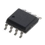
| 描述 | IC OPAMP LOGARITHMIC 45KHZ 8SOIC对数放大器 LOGARITHMIC AMP |
| 产品分类 | Linear - Amplifiers - Instrumentation, OP Amps, Buffer Amps集成电路 - IC |
| 品牌 | Texas Instruments |
| 产品手册 | http://www.ti.com/litv/sbos242b |
| 产品图片 |
|
| rohs | 符合RoHS无铅 / 符合限制有害物质指令(RoHS)规范要求 |
| 产品系列 | 放大器 IC,对数放大器,Texas Instruments LOG101AID- |
| 数据手册 | |
| 产品型号 | LOG101AID |
| 产品 | Logarithmic Amplifiers |
| 产品目录页面 | |
| 产品种类 | 对数放大器 |
| 供应商器件封装 | 8-SOIC |
| 共模抑制比—最小值 | 105 dB |
| 其它名称 | 296-12850-5 |
| 包装 | 管件 |
| 单位重量 | 76 mg |
| 压摆率 | - |
| 商标 | Texas Instruments |
| 增益带宽积 | - |
| 安装类型 | 表面贴装 |
| 安装风格 | SMD/SMT |
| 封装 | Tube |
| 封装/外壳 | 8-SOIC(0.154",3.90mm 宽) |
| 封装/箱体 | SOIC-8 |
| 工作温度 | -5°C ~ 75°C |
| 工作温度范围 | - 40 C to + 85 C |
| 工作电源电压 | 36 V |
| 工厂包装数量 | 75 |
| 放大器类型 | 对数和对数比率 |
| 标准包装 | 75 |
| 电压-电源,单/双 (±) | ±4.5 V ~ 18 V |
| 电压-输入失调 | 300µV |
| 电流-电源 | 1mA |
| 电流-输入偏置 | 5pA |
| 电流-输出/通道 | 18mA |
| 电源电流 | 10 mA |
| 电路数 | 1 |
| 系列 | LOG101 |
| 输入电压范围—最大 | 0.5 V |
| 输入补偿电压 | 1.5 mV |
| 输出类型 | - |
| 通道数量 | 1 Channel |


PDF Datasheet 数据手册内容提取
LOG101 LOG101 SBOS242B – MAY 2002 – REVISED JUNE 2004 Precision LOGARITHMIC AND LOG RATIO AMPLIFIER FEATURES DESCRIPTION (cid:1) EASY-TO-USE COMPLETE CORE FUNCTION The LOG101 is a versatile integrated circuit that computes the logarithm or log ratio of an input current relative to a (cid:1) HIGH ACCURACY: 0.01% FSO Over 5 Decades reference current. (cid:1) WIDE INPUT DYNAMIC RANGE: The LOG101 is tested over a wide dynamic range of input 7.5 Decades, 100pA to 3.5mA signals. In log ratio applications, a signal current can come (cid:1) LOW QUIESCENT CURRENT: 1mA from a photodiode, and a reference current from a resistor in (cid:1) WIDE SUPPLY RANGE: ±4.5V to ±18V series with a precision external reference. The output signal at V is trimmed to 1V per decade of input OUT current allowing seven decades of input current dynamic APPLICATIONS range. (cid:1) LOG, LOG RATIO COMPUTATION: Low DC offset voltage and temperature drift allow accurate measurement of low-level signals over a wide environmental Communication, Analytical, Medical, Industrial, temperature range. The LOG101 is specified over the tem- Test, and General Instrumentation perature range –5°C to +75°C, with operation over (cid:1) PHOTODIODE SIGNAL COMPRESSION AMPS –40°C to +85°C. (cid:1) ANALOG SIGNAL COMPRESSION IN FRONT Note: Protected under US Patent #6,667,650; other patents pending. OF ANALOG-TO-DIGITAL (A/D) CONVERTERS I 2 VOUT = (1V) • LOG (I1/I2) CC V+ 4 8 I 1 LOG101 1 Q Q 1 2 3 A1 A2 VOUT R 2 R 1 5 6 GND V– Please be aware that an important notice concerning availability, standard warranty, and use in critical applications of Texas Instruments semiconductor products and disclaimers thereto appears at the end of this data sheet. All trademarks are the property of their respective owners. PRODUCTION DATA information is current as of publication date. Copyright © 2002-2004, Texas Instruments Incorporated Products conform to specifications per the terms of Texas Instruments standard warranty. Production processing does not necessarily include testing of all parameters. www.ti.com
ABSOLUTE MAXIMUM RATINGS(1) ELECTROSTATIC Supply Voltage, V+ to V–....................................................................36V DISCHARGE SENSITIVITY Input Voltage....................................................(V–) – 0.5 to (V+) + 0.5V Input Current...................................................................................±10mA This integrated circuit can be damaged by ESD. Texas Instru- Output Short-Circuit(2)..............................................................Continuous ments recommends that all integrated circuits be handled with Operating Temperature....................................................–40°C to +85°C Storage Temperature.....................................................–55°C to +125°C appropriate precautions. Failure to observe proper handling Junction Temperature....................................................................+150°C and installation procedures can cause damage. Lead Temperature (soldering, 10s)...............................................+300°C ESD damage can range from subtle performance degrada- NOTES: (1) Stresses above these ratings may cause permanent damage. tion to complete device failure. Precision integrated circuits Exposure to absolute maximum conditions for extended periods may degrade may be more susceptible to damage because very small device reliability. (2) Short-circuit to ground. parametric changes could cause the device not to meet its published specifications. PIN DESCRIPTION Top View SO I 1 8 I 1 2 NC 2 7 NC LOG101 V 3 6 GND OUT V+ 4 5 V– NC = No Internal Connection PACKAGE/ORDERING INFORMATION(1) SPECIFIED PACKAGE TEMPERATURE PACKAGE ORDERING TRANSPORT PRODUCT PACKAGE-LEAD DESIGNATOR RANGE MARKING NUMBER MEDIA, QUANTITY LOG101AID SO-8 D –5°C to +75°C LOG101 LOG101AID Rails, 100 " " " " " LOG101AIDR Tape and Reel, 2500 NOTE: (1) For the most current package and ordering information, see the Package Option Addendum located at the end of this data sheet. ELECTRICAL CHARACTERISTICS ° ° Boldface limits apply over the specified temperature range, T = –5 C to +75 C. A At T = +25°C, V = ±5V, and R = 10kΩ, unless otherwise noted. A S OUT LOG101AID PARAMETER CONDITION MIN TYP MAX UNITS CORE LOG FUNCTION I /V Equation V = (1V) • log (I/I) V IN OUT O 1 2 LOG CONFORMITY ERROR(1) Initial 1nA to 100µA (5 decades) 0.01 0.2 % 100pA to 3.5mA (7.5 decades) 0.06 % over Temperature 1nA to 100µA (5 decades) 0.0001 %/°C 100pA to 3.5mA (7.5 decades)(2) 0.0005 %/°C GAIN(3) Initial Value 1nA to 100µA 1 V/decade Gain Error 1nA to 100µA 0.15 ±1 % vs Temperature T to T 0.003 0.01 %/°C MIN MAX INPUT, A1 and A2 Offset Voltage ±0.3 ±1.5 mV vs Temperature T to T ±2 µV/°C MIN MAX vs Power Supply (PSRR) V = ±4.5V to ±18V 5 50 µV/V S Input Bias Current ±5 pA vs Temperature T to T Doubles Every 10°C MIN MAX Voltage Noise f = 10Hz to 10kHz 3 µVrms f = 1kHz 30 nV/√Hz Current Noise f = 1kHz 4 fA/√Hz Common-Mode Voltage Range (Positive) (V+) – 2 (V+) – 1.5 V (Negative) (V–) + 2 (V–) + 1.2 V Common-Mode Rejection Ratio (CMRR) 105 dB OUTPUT, A2 (V ) OUT Output Offset, V , Initial ±3 ±15 mV OSO vs Temperature T to T ±2 µV/°C MIN MAX Full-Scale Output (FSO) V = ±5V (V–) + 1.2 (V+) – 1.5 V S Short-Circuit Current ±18 mA LOG101 2 www.ti.com SBOS242B
ELECTRICAL CHARACTERISTICS (Cont.) ° ° Boldface limits apply over the specified temperature range, T = –5 C to +75 C. A At T = +25°C, V = ±5V, and R = 10kΩ, unless otherwise noted. A S L LOG101AID PARAMETER CONDITION MIN TYP MAX UNITS TOTAL ERROR(4)(5) I or I remains fixed while other varies. 1 2 Initial Min to Max I or I = 3.5mA ±75 mV 1 2 I or I = 1mA ±20 mV 1 2 I or I = 100µA ±20 mV 1 2 I or I = 10µA ±20 mV 1 2 I or I = 1µA ±20 mV 1 2 I or I = 100nA ±20 mV 1 2 I or I = 10nA ±20 mV 1 2 I or I = 1nA ±20 mV 1 2 I or I = 350pA ±20 mV 1 2 I or I = 100pA ±20 mV 1 2 vs Temperature I or I = 3.5mA ±1.2 mV/°C 1 2 I or I = 1mA ±0.4 mV/°C 1 2 I or I = 100µA ±0.1 mV/°C 1 2 I or I = 10µA ±0.05 mV/°C 1 2 I or I = 1µA ±0.05 mV/°C 1 2 I or I = 100nA ±0.09 mV/°C 1 2 I or I = 10nA ±0.2 mV/°C 1 2 I or I = 1nA ±0.3 mV/°C 1 2 I or I = 350pA ±0.1 mV/°C 1 2 I or I = 100pA ±0.3 mV/°C 1 2 vs Supply I or I = 3.5mA ±3.0 mV/V 1 2 I or I = 1mA ±0.1 mV/V 1 2 I or I = 100µA ±0.1 mV/V 1 2 I or I = 10µA ±0.1 mV/V 1 2 I or I = 1µA ±0.1 mV/V 1 2 I or I = 100nA ±0.1 mV/V 1 2 I or I = 10nA ±0.1 mV/V 1 2 I or I = 1nA ±0.25 mV/V 1 2 I or I = 350pA ±0.1 mV/V 1 2 I or I = 100pA ±0.1 mV/V 1 2 FREQUENCY RESPONSE, CORE LOG(6) BW, 3dB I = 10nA C = 4500pF 0.1 kHz 2 C I = 1µA C = 150pF 38 kHz 2 C I = 10µA C = 150pF 40 kHz 2 C I = 1mA C = 50pF 45 kHz 2 C Step Response Increasing I = 1µA to 1mA C = 150pF 11 µs 2 C I = 100nA to 1µA C = 150pF 7 µs 2 C I = 10nA to 100nA C = 150pF 110 µs 2 C Decreasing I = 1mA to 1µA C = 150pF 45 µs 2 C I = 1µA to 100nA C = 150pF 20 µs 2 C I = 100nA to 10nA C = 150pF 550 µs 2 C POWER SUPPLY Operating Range V ±4.5 ±18 V S Quiescent Current I = 0 ±1 ±1.5 mA O TEMPERATURE RANGE Specified Range, T to T –5 75 °C MIN MAX Operating Range –40 85 °C Storage Range –55 125 °C Thermal Resistance, θ SO-8 150 °C/W JA NOTES:(1)Log Conformity Error is peak deviation from the best-fit straight line of V versus log (I /I) curve expressed as a percent of peak-to-peak full-scale. OUT 1 2 (2)May require higher supply for full dynamic range. (3)Output core log function is trimmed to 1V output per decade change of input current. (4)Worst-case Total Error for any ratio of I /I is the largest of the two errors, when I and I are considered separately. 1 2 1 2 (5)Total I + I should be kept below 4.5mA on ±5V supply. 1 2 (6)Bandwidth (3dB) and transient response are a function of both the compensation capacitor and the level of input current. LOG101 3 SBOS242B www.ti.com
TYPICAL CHARACTERISTICS At T = +25°C, V = ±5V, and R = 10kΩ, unless otherwise noted. A S L NORMALIZED TRANSFER FUNCTION ONE CYCLE OF NORMALIZED TRANSFER FUNCTION 4.0 1 V = 1V LOG (I/I) V) 3.0 OUT 1 2 V) 0.9 Output Voltage ( 210...000 Output Voltage ( 0000....8765 malized ––12..00 malized 00..43 Nor –3.0 Nor 0.2 0.1 –4.0 0 0.0001 0.001 0.01 0.1 1 10 100 1k 10k 1 2 3 4 6 8 10 Current Ratio, I/I 1 2 Current Ratio, I/I 1 2 TOTAL ERROR vs INPUT CURRENT GAIN ERROR (I2 = 1µA) 120 5.8 +85°C 100 4.8 +75°C +75°C Error (mV) 8600 Error (%) 32..88 –5°C to –4+02°C5°C Total 40 Gain 1.8 +25°C –5°C 20 0.8 0 –0.2 100pA 1nA 10nA 100nA 1µA 10µA 100µA 1mA 10mA 100pA 1nA 10nA 100nA 1µA 10µA 100µA 1mA 10mA Input Current (I or I) Input Current (I or I) 1 2 1 2 MINIMUM VALUE OF COMPENSATION CAPACITOR 3dB FREQUENCY RESPONSE 100M 1M C (pF)C 110101001MMkkk Sabneeldloe wIc2t 2mCpaCFx f .om Vra aIy1l uI m1be e=isn 1 i1.gµ0InA10o =nr eA1Id10. n=A 1nI1A = 100pA uency Response (Hz) 110100010kkk 1nA 1001µ0AnA C1C µ= A1 0 p F 11000µIµ1A A= 1nA1 0µ1A0 tno A1µ A 111t111I1o00mµm0 =0001AAA µnµ01 AµAAmAA 10100 I11 =0 01µ0AµA 3dB Freq 101 C C = 1 0 0 0 p F C C = 1µ F 1I10 =n A1nA 1mA 1 0.1 100pA 1nA 10nA 100nA 1µA 10µA 100µA 1mA 10mA 100pA 1nA 10nA 100nA 1µA 10µA 100µA 1mA I2 I2 LOG101 4 www.ti.com SBOS242B
TYPICAL CHARACTERISTICS (Cont.) At T = +25°C, V = ±5V, and R = 10kΩ, unless otherwise noted. A S L LOG CONFORMITY vs INPUT CURRENT LOG CONFORMITY vs TEMPERATURE 17 350 15 7 Decades 300 (100pA to 1mA) 13 V) +85°C %) 250 m 11 m y ( y ( 6 Decades mit 9 mit 200 (1nA to 1mA) or or Conf 7 +75°C Conf 150 5 Decades Log 5 –40°C to +25°C Log 100 (1nA to 100µA) 3 50 1 –1 0 100pA 1nA 10nA 100nA 1µA 10µA 100µA 1mA –40 –30–20 –10 0 10 20 30 40 50 60 70 80 90 Input Current (I1 or I2) Temperature (°C) APPLICATION INFORMATION INPUT CURRENT RANGE To maintain specified accuracy, the input current range of the The LOG101 is a true logarithmic amplifier that uses the LOG101 should be limited from 100pA to 3.5mA. Input currents base-emitter voltage relationship of bipolar transistors to outside of this range may compromise LOG101 performance. compute the logarithm, or logarithmic ratio of a current ratio. Input currents larger than 3.5mA result in increased Figure 1 shows the basic connections required for operation nonlinearity. An absolute maximum input current rating of of the LOG101. In order to reduce the influence of lead 10mA is included to prevent excessive power dissipation that inductance of power-supply lines, it is recommended that may damage the logging transistor. each supply be bypassed with a 10µF tantalum capacitor in On ±5V supplies, the total input current (I + I ) is limited to parallel with a 1000pF ceramic capacitor, as shown in 1 2 4.5mA. Due to compliance issues internal to the LOG101, to Figure 1. Connecting the capacitors as close to the LOG101 accommodate larger total input currents, supplies should be as possible will contribute to noise reduction as well. increased. Currents smaller than 100pA will result in increased errors due to the input bias currents of op amps A and A (typically 5pA). 1 2 The input bias currents may be compensated for, as shown in Figure 2. The input stages of the amplifiers have FET inputs, V+ with input bias current doubling every 10°C, which makes the nulling technique shown practical only where the temperature 10µF 1000pF is fairly stable. 4 R 1 10k2Ω V– V+ 6 3 LOG101 VOUT R1 1MΩ 5 1 3 8 V OUT 5 I1 I I LOG101 1 2 C C 8 6 GND 10µF 1000pF I2 R> 11'MΩ 4 V– C C V– R' 2 10kΩ V+ FIGURE 1. Basic Connections of the LOG101. FIGURE 2. Bias Current Nulling. LOG101 5 SBOS242B www.ti.com
SETTING THE REFERENCE CURRENT V+ V+ When the LOG101 is used to compute logarithms, either I or 1 I1 = 2.5nA to 1mA 4 I can be held constant and becomes the reference current to 2.5V 1 3 2 REF3025 which the other is compared. 1GΩ to 2.5kΩ VOUT VOUT is expressed as: 100kΩ I2 = 2.5nA LOG101 10MΩ V = (1V) • log (I /I ) (1) 8 OUT 1 2 +25mV I can be derived from an external current source (such as 3 5 6GND REF +2.5V C shown in Figure 3), or it may be derived from a voltage 100Ω C V– source with one or more resistors. When a single resistor is OPA335 Chopper Op Amp used, the value may be large depending on I . If I is REF REF 10nA and +2.5V is used: –2.5V R = 2.5V/10nA = 250MΩ (2) REF FIGURE 5. Current Source with Offset Compensation. I REF 2N2905 at different levels of input signals. Smaller input currents R require greater gains to maintain full dynamic range, and will REF 3.6kΩ slow the frequency response of the LOG101. 2N2905 +15V –15V 6V IN834 6V FREQUENCY COMPENSATION I = REF R REF Frequency compensation for the LOG101 is obtained by FIGURE 3. Temperature Compensated Current Source. connecting a capacitor between pins 3 and 8. The size of the capacitor is a function of the input currents, as shown in the A voltage divider may be used to reduce the value of the Typical Characteristic Curves (Minimum Value of Compen- resistor, as shown in Figure 4. When using this method, one sation Capacitor). For any given application, the smallest must consider the possible errors caused by the amplifier’s value of the capacitor which may be used is determined by input offset voltage. The input offset voltage of amplifier A1 the maximum value of I2 and the minimum value of I1. Larger has a maximum value of 1.5mV, making VREF a suggested values of CC will make the LOG101 more stable, but will value of 100mV. reduce the frequency response. In an application, highest overall bandwidth can be achieved by detecting the signal level at V , then switching in OUT V = 100mV appropriate values of compensation capacitors. REF V R R OS 1 3 + – +5V 1 NEGATIVE INPUT CURRENTS R IREF A1 The LOG101 will function only with positive input currents 2 R >> R (conventional current flows into pins 1 and 8). In situations 3 2 where negative input currents are needed, the circuits in Figures 6, 7, and 8 may be used. FIGURE 4. T Network for Reference Current. Figure 5 shows a low-level current source using a series resistor. The low offset op-amp reduces the effect of the LOG101’s input offset voltage. Q Q I A B IN National FREQUENCY RESPONSE LM394 The frequency response curve seen in the Typical Charac- D D teristic Curves is shown for constant DC I and I with a small 1 2 1 2 signal AC current on one input. The 3dB frequency response of the LOG101 is a function of the magnitude of the input current levels and of the value of the OPA703 I frequency compensation capacitor. See Typical Characteristic OUT Curve “3dB Frequency Response” for details. The transient response of the LOG101 is different for in- creasing and decreasing signals. This is due to the fact that a log amp is a nonlinear gain element and has different gains FIGURE 6. Current Inverter/Current Source. LOG101 6 www.ti.com SBOS242B
V+ +5V +3.3V TLV271 or12OPA2335 I1 1 4 3 1/2 OPA2335 V OUT 1.5kΩ Sample D1 λ λ ´ LOG101 1.5kΩ +5V 1 1 I 2 8 6 10nA to 1mA Back Bias 1/2 OPA2335 BSH203 SLoiugrhcte λ1 D2 5 +3.3V C LOG101 C 10nA to 1mA Pin 1 or Pin 8 Photodiode V– FIGURE 9. Absorbance Measurement. FIGURE 7. Precision Current Inverter/Current Source. OPERATION ON SINGLE SUPPLY Many applications do not have the dual supplies required to VOLTAGE INPUTS operate the LOG101. Figure 10 shows the LOG101 config- The LOG101 gives the best performance with current inputs. ured for operation with a single +5V supply. Voltage inputs may be handled directly with series resistors, but the dynamic input range is limited to approximately three decades of input voltage by voltage noise and offsets. The transfer function of Equation (13) applies to this configuration. Single Supply +5V 4 1 3 APPLICATION CIRCUITS V OUT I LOG RATIO 1 LOG101 6 One of the more common uses of log ratio amplifiers is 8 to measure absorbance. A typical application is shown in 5 Figure 9. I 2 C Absorbance of the sample is A = logλ ´/λ (3) C 1 1 1µF If D1 and D2 are matched A ∝ (1V) logI1/I2 (4) 3 5 2 1 TPS(1) –5V DATA COMPRESSION 1µF 4 1µF NOTE: (1) TPS60402DBV negative charge pump. In many applications the compressive effects of the logarith- mic transfer function are useful. For example, a LOG101 preceding a 12-bit Analog-to-Digital (A/D) converter can FIGURE 10. Single +5V Power-Supply Operation. produce the dynamic range equivalent to a 20-bit converter. 1.5kΩ 100kΩ 100kΩ +5V 10nA to 1mA +3.3V Back Bias 1/2 +5V 1.5kΩ +3.3V OPA2335 1/2 Photodiode OPA2335 1.5kΩ 100kΩ 100kΩ LOG101 10nA to 1mA Pin 1 or Pin 8 FIGURE 8. Precision Current Inverter/Current Source. LOG101 7 SBOS242B www.ti.com
INSIDE THE LOG101 Using the base-emitter voltage relationship of matched also bipolar transistors, the LOG101 establishes a logarith- mic function of input current ratios. Beginning with the V =V R1+R2 base-emitter voltage defined as: OUT L R (9) 1 R +R I I kT V = 1 2 nV log 1 (10) V =V ln C where:V = (1) OUT R T I BE T I T q 1 2 S k = Boltzman’s constant = 1.381 • 10–23 V =(1V)•logI1 or OUT I (11) T = Absolute temperature in degrees Kelvin 2 q = Electron charge = 1.602 • 10–19 Coulombs I = Collector current C I = Reverse saturation current S I2 Q1 – – Q2 From the circuit in Figure 11, we see that: I1 + + VOUT A V =V –V I VBE1 VBE2 2 L BE1 BE2 (2) 1 A 1 I Substituting (1) into (2) yields: VOUT = (1V) • LOG I1 R2 2 V I I I L V =V ln 1 –V ln 2 (3) 2 L T1 IS1 T2 IS2 R1 If the transistors are matched and isothermal and V = V , then (3) becomes: TI T2 FIGURE 11. Simplified Model of a Log Amplifier. I I V =V ln 1 –ln 2 (4) L T1 I I It should be noted that the temperature dependance S S V =V lnI1 andsince (5) associated with VT = kT/q is internally compensated on L T I2 the LOG101 by making R1 a temperature sensitive resis- lnx=2.3log x (6) tor with the required positive temperature coefficient. 10 I V =nV log 1 (7) L T I 2 where n = 2.3 (8) DEFINITION OF TERMS 3.5 TThReA iNdeSaFl EtraRn sFfUerN fVuCnTcItOi o=nN 1isV: • log (I /I ) (5) 3221....0055 III 2 22 === 1110n00AnpAA OUT 1 2 1.0 FoAAwvichCgecauCrutr revUama c1Rloiy2dAr ecsoC ohpcnoYeoswrmiadstp eitnlrhiagceta irogtaenrndasg p efthoh icrfao anarl trlfhoeoegpr rLeroaOsthteiGoen r1t aa0amt1imo.pnpli floiieffi ert rhaser.e t Trashonisms feeisr- V(V)OUT ––––––00322101........50005055 100pAIIIII 22222===== 111111nµ000mAµ00AAµnAAA10nA 100nAVO1µUTA = (11V0µ) A• LO1G00 µ(I1A/I21)m A 10mI1A because the transfer function is nonlinear and has two –3.5 inputs, each of which can vary over a wide dynamic range. The accuracy for any combination of inputs is determined FIGURE 12. Transfer Function with Varying I and I . 2 1 from the total error specification. LOG101 8 www.ti.com SBOS242B
TOTAL ERROR to I is shown in Figure 13. The OPA703 is configured as a 2 level shifter with inverting gain and is used to scale the The total error is the deviation (expressed in mV) of the photodiode current directly into the A/D converter input actual output from the ideal output of V = 1V • log (I /I ). OUT 1 2 voltage range. Thus, The wide dynamic range of the LOG101 is also useful for V = V ± Total Error. (6) OUT(ACTUAL) OUT(IDEAL) measuring avalanche photodiode current (APD) (see Figure 14). It represents the sum of all the individual components of error normally associated with the log amp when operated in the LOG CONFORMITY current input mode. The worst-case error for any given ratio For the LOG101, log conformity is calculated the same as of I1/I2 is the largest of the two errors when I1 and I2 are linearity and is plotted I1/I2 on a semi-log scale. In many considered separately. Temperature can affect total error. applications, log conformity is the most important specifica- tion. This is because bias current errors are negligible ERRORS RTO AND RTI (5pA compared to input currents of 100pA and above) and the scale factor and offset errors may be trimmed to zero or As with any transfer function, errors generated by the func- removed by system calibration. This leaves log conformity as tion itself may be Referred-to-Output (RTO) or Referred-to- the major source of error. Input (RTI). In this respect, log amps have a unique property: Log conformity is defined as the peak deviation from the best Given some error voltage at the log amp’s output, that error fit straight line of the V versus log (I /I ) curve. This is corresponds to a constant percent of the input regardless of OUT 1 2 expressed as a percent of ideal full-scale output. Thus, the the actual input level. nonlinearity error expressed in volts over m decades is: (7) V = 1V/dec • 2NmV USING A LARGER REFERENCE VOLTAGE OUT(NONLIN) REDUCES OFFSET ERRORS where N is the log conformity error, in percent. Using a larger reference voltage to create the reference current minimizes errors due to the LOG101’s input offset INDIVIDUAL ERROR COMPONENTS voltage. Maintaining an increasing output voltage as a func- The ideal transfer function with current input is: tion of increasing photodiode current is also important in (8) many optical sensing applications. All zeros from the V =(1V)• logI1 A/D converter output represent zero or low-scale photodiode OUT I 2 current. Inputting the reference current into I , and designing 1 The actual transfer function with the major components of I such that it is as large or larger than the expected REF error is: maximum photodiode current is accomplished using this (9) requirement. The LOG101 configured with the reference V =(1V)(1±∆K)log I1–IB1 ±2Nm±V current connecting I1 and the photodiode current connecting OUT I –I OSO 2 B2 V R ( I ) I = REF V = V – 2 • (1V)LOG REF REF R1 OUT REF R3 IPHOTO R2 R3 CC VOUT 3 V to V MIN MAX I REF R I 1 1 Q Q 1 1 2 OPA703 A/D Converter A V 2 REF A 1 R 2 I PHOTO I 2 R 8 3 LOG101 I to I MIN MAX 6 FIGURE 13. Technique for Using Full-Scale Reference Current Such that V Increases with Increasing Photodiode Current. OUT LOG101 9 SBOS242B www.ti.com
I SHUNT +15V to +60V 500Ω Irx = 1µA to 1mA Receiver 5kΩ 5kΩ 10Gbits/sec +5V APD I to V Converter INA168 SOT23-5 IOUT = 0.1 • ISHUNT 2 1 I OUT CC 1.2kΩ 1kΩ +5V 4 3 1 Q Q 1 2 OPA703 V = 2.5V to 0V OUT A 2 A 1 100µA 25kΩ 8 REF3025 LOG101 SO-8 2.5V 5 6 –5V FIGURE 14. High Side Shunt for Avalanche Photodiode (APD) Measures 3-Decades of APD Current. The individual component of error is: Since the ideal output is 1.000V, the error as a percent of ∆K = gain accuracy (0.15%, typ), as specified in the reading is specification table. 0.005055 %error= •100%=0.5% (12) IB1 = bias current of A1 (5pA, typ) 1 I = bias current of A (5pA, typ) B2 2 For the case of voltage inputs, the actual transfer function is N = log conformity error (0.01%, 0.06%, typ) 0.01% for n = 5, 0.06% for n = 7 V1–I ±EOS1 VOSO = output offset voltage (3mV, typ) VOUT =(1V)(1±∆K)log VR21–IB1 ±ERO1S2 ±2Nn±VOSO (13) n = number of decades over which N is specified: R B2 R 2 2 Example: what is the error when E E I = 1µA and I = 100nA (10) Where ROS1and ROS2 are considered to be zero for large 1 2 1 2 V =(1±0.0015)log10−6 −5•10−12 ±(2)(0.0001)5±3.0mV values of resistance from external input current sources. OUT 10−7 −5•10−12 = 1.005055V (11) LOG101 10 www.ti.com SBOS242B
PACKAGE OPTION ADDENDUM www.ti.com 6-Feb-2020 PACKAGING INFORMATION Orderable Device Status Package Type Package Pins Package Eco Plan Lead/Ball Finish MSL Peak Temp Op Temp (°C) Device Marking Samples (1) Drawing Qty (2) (6) (3) (4/5) LOG101AID ACTIVE SOIC D 8 75 Green (RoHS NIPDAU Level-3-260C-168 HR -40 to 85 LOG & no Sb/Br) 101A LOG101AIDE4 ACTIVE SOIC D 8 75 Green (RoHS NIPDAU Level-3-260C-168 HR -40 to 85 LOG & no Sb/Br) 101A LOG101AIDR ACTIVE SOIC D 8 2500 Green (RoHS NIPDAU Level-3-260C-168 HR -40 to 85 LOG & no Sb/Br) 101A (1) The marketing status values are defined as follows: ACTIVE: Product device recommended for new designs. LIFEBUY: TI has announced that the device will be discontinued, and a lifetime-buy period is in effect. NRND: Not recommended for new designs. Device is in production to support existing customers, but TI does not recommend using this part in a new design. PREVIEW: Device has been announced but is not in production. Samples may or may not be available. OBSOLETE: TI has discontinued the production of the device. (2) RoHS: TI defines "RoHS" to mean semiconductor products that are compliant with the current EU RoHS requirements for all 10 RoHS substances, including the requirement that RoHS substance do not exceed 0.1% by weight in homogeneous materials. Where designed to be soldered at high temperatures, "RoHS" products are suitable for use in specified lead-free processes. TI may reference these types of products as "Pb-Free". RoHS Exempt: TI defines "RoHS Exempt" to mean products that contain lead but are compliant with EU RoHS pursuant to a specific EU RoHS exemption. Green: TI defines "Green" to mean the content of Chlorine (Cl) and Bromine (Br) based flame retardants meet JS709B low halogen requirements of <=1000ppm threshold. Antimony trioxide based flame retardants must also meet the <=1000ppm threshold requirement. (3) MSL, Peak Temp. - The Moisture Sensitivity Level rating according to the JEDEC industry standard classifications, and peak solder temperature. (4) There may be additional marking, which relates to the logo, the lot trace code information, or the environmental category on the device. (5) Multiple Device Markings will be inside parentheses. Only one Device Marking contained in parentheses and separated by a "~" will appear on a device. If a line is indented then it is a continuation of the previous line and the two combined represent the entire Device Marking for that device. (6) Lead/Ball Finish - Orderable Devices may have multiple material finish options. Finish options are separated by a vertical ruled line. Lead/Ball Finish values may wrap to two lines if the finish value exceeds the maximum column width. Important Information and Disclaimer:The information provided on this page represents TI's knowledge and belief as of the date that it is provided. TI bases its knowledge and belief on information provided by third parties, and makes no representation or warranty as to the accuracy of such information. Efforts are underway to better integrate information from third parties. TI has taken and continues to take reasonable steps to provide representative and accurate information but may not have conducted destructive testing or chemical analysis on incoming materials and chemicals. TI and TI suppliers consider certain information to be proprietary, and thus CAS numbers and other limited information may not be available for release. Addendum-Page 1
PACKAGE OPTION ADDENDUM www.ti.com 6-Feb-2020 In no event shall TI's liability arising out of such information exceed the total purchase price of the TI part(s) at issue in this document sold by TI to Customer on an annual basis. Addendum-Page 2
PACKAGE MATERIALS INFORMATION www.ti.com 14-Jul-2012 TAPE AND REEL INFORMATION *Alldimensionsarenominal Device Package Package Pins SPQ Reel Reel A0 B0 K0 P1 W Pin1 Type Drawing Diameter Width (mm) (mm) (mm) (mm) (mm) Quadrant (mm) W1(mm) LOG101AIDR SOIC D 8 2500 330.0 12.4 6.4 5.2 2.1 8.0 12.0 Q1 PackMaterials-Page1
PACKAGE MATERIALS INFORMATION www.ti.com 14-Jul-2012 *Alldimensionsarenominal Device PackageType PackageDrawing Pins SPQ Length(mm) Width(mm) Height(mm) LOG101AIDR SOIC D 8 2500 367.0 367.0 35.0 PackMaterials-Page2
PACKAGE OUTLINE D0008A SOIC - 1.75 mm max height SCALE 2.800 SMALL OUTLINE INTEGRATED CIRCUIT C SEATING PLANE .228-.244 TYP [5.80-6.19] .004 [0.1] C A PIN 1 ID AREA 6X .050 [1.27] 8 1 2X .189-.197 [4.81-5.00] .150 NOTE 3 [3.81] 4X (0 -15 ) 4 5 8X .012-.020 B .150-.157 [0.31-0.51] .069 MAX [3.81-3.98] .010 [0.25] C A B [1.75] NOTE 4 .005-.010 TYP [0.13-0.25] 4X (0 -15 ) SEE DETAIL A .010 [0.25] .004-.010 0 - 8 [0.11-0.25] .016-.050 [0.41-1.27] DETAIL A (.041) TYPICAL [1.04] 4214825/C 02/2019 NOTES: 1. Linear dimensions are in inches [millimeters]. Dimensions in parenthesis are for reference only. Controlling dimensions are in inches. Dimensioning and tolerancing per ASME Y14.5M. 2. This drawing is subject to change without notice. 3. This dimension does not include mold flash, protrusions, or gate burrs. Mold flash, protrusions, or gate burrs shall not exceed .006 [0.15] per side. 4. This dimension does not include interlead flash. 5. Reference JEDEC registration MS-012, variation AA. www.ti.com
EXAMPLE BOARD LAYOUT D0008A SOIC - 1.75 mm max height SMALL OUTLINE INTEGRATED CIRCUIT 8X (.061 ) [1.55] SYMM SEE DETAILS 1 8 8X (.024) [0.6] SYMM (R.002 ) TYP [0.05] 5 4 6X (.050 ) [1.27] (.213) [5.4] LAND PATTERN EXAMPLE EXPOSED METAL SHOWN SCALE:8X SOLDER MASK SOLDER MASK METAL OPENING OPENING METAL UNDER SOLDER MASK EXPOSED METAL EXPOSED METAL .0028 MAX .0028 MIN [0.07] [0.07] ALL AROUND ALL AROUND NON SOLDER MASK SOLDER MASK DEFINED DEFINED SOLDER MASK DETAILS 4214825/C 02/2019 NOTES: (continued) 6. Publication IPC-7351 may have alternate designs. 7. Solder mask tolerances between and around signal pads can vary based on board fabrication site. www.ti.com
EXAMPLE STENCIL DESIGN D0008A SOIC - 1.75 mm max height SMALL OUTLINE INTEGRATED CIRCUIT 8X (.061 ) [1.55] SYMM 1 8 8X (.024) [0.6] SYMM (R.002 ) TYP [0.05] 5 4 6X (.050 ) [1.27] (.213) [5.4] SOLDER PASTE EXAMPLE BASED ON .005 INCH [0.125 MM] THICK STENCIL SCALE:8X 4214825/C 02/2019 NOTES: (continued) 8. Laser cutting apertures with trapezoidal walls and rounded corners may offer better paste release. IPC-7525 may have alternate design recommendations. 9. Board assembly site may have different recommendations for stencil design. www.ti.com
IMPORTANTNOTICEANDDISCLAIMER TI PROVIDES TECHNICAL AND RELIABILITY DATA (INCLUDING DATASHEETS), DESIGN RESOURCES (INCLUDING REFERENCE DESIGNS), APPLICATION OR OTHER DESIGN ADVICE, WEB TOOLS, SAFETY INFORMATION, AND OTHER RESOURCES “AS IS” AND WITH ALL FAULTS, AND DISCLAIMS ALL WARRANTIES, EXPRESS AND IMPLIED, INCLUDING WITHOUT LIMITATION ANY IMPLIED WARRANTIES OF MERCHANTABILITY, FITNESS FOR A PARTICULAR PURPOSE OR NON-INFRINGEMENT OF THIRD PARTY INTELLECTUAL PROPERTY RIGHTS. These resources are intended for skilled developers designing with TI products. You are solely responsible for (1) selecting the appropriate TI products for your application, (2) designing, validating and testing your application, and (3) ensuring your application meets applicable standards, and any other safety, security, or other requirements. These resources are subject to change without notice. TI grants you permission to use these resources only for development of an application that uses the TI products described in the resource. Other reproduction and display of these resources is prohibited. No license is granted to any other TI intellectual property right or to any third party intellectual property right. TI disclaims responsibility for, and you will fully indemnify TI and its representatives against, any claims, damages, costs, losses, and liabilities arising out of your use of these resources. TI’s products are provided subject to TI’s Terms of Sale (www.ti.com/legal/termsofsale.html) or other applicable terms available either on ti.com or provided in conjunction with such TI products. TI’s provision of these resources does not expand or otherwise alter TI’s applicable warranties or warranty disclaimers for TI products. Mailing Address: Texas Instruments, Post Office Box 655303, Dallas, Texas 75265 Copyright © 2020, Texas Instruments Incorporated