ICGOO在线商城 > 集成电路(IC) > PMIC - AC-DC 转换器,离线开关 > LNK354GN

 Datasheet下载
- 型号: LNK354GN
- 制造商: Power Integrations
- 库位|库存: xxxx|xxxx
- 要求:
| 数量阶梯 | 香港交货 | 国内含税 |
| +xxxx | $xxxx | ¥xxxx |
查看当月历史价格
查看今年历史价格
LNK354GN产品简介:
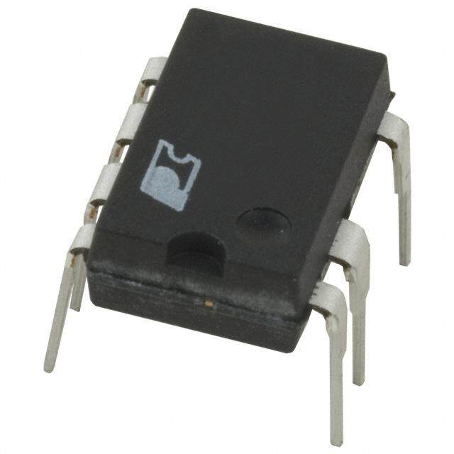
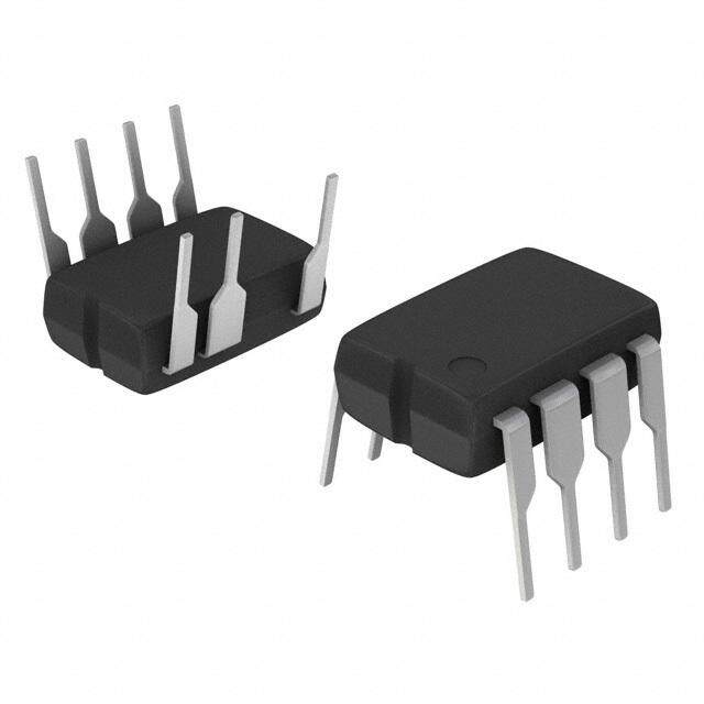
ICGOO电子元器件商城为您提供LNK354GN由Power Integrations设计生产,在icgoo商城现货销售,并且可以通过原厂、代理商等渠道进行代购。 LNK354GN价格参考¥5.36-¥5.70。Power IntegrationsLNK354GN封装/规格:PMIC - AC-DC 转换器,离线开关, Converter Offline Flyback Topology 200kHz SMD-8B。您可以下载LNK354GN参考资料、Datasheet数据手册功能说明书,资料中有LNK354GN 详细功能的应用电路图电压和使用方法及教程。
| 参数 | 数值 |
| 产品目录 | 集成电路 (IC)半导体 |
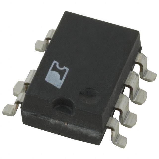
| 描述 | IC OFFLINE SWIT OCP HV 8SMD交流/直流转换器 4.5 W (85-265 VAC) 5 W (230 VAC) |
| 产品分类 | |
| 品牌 | Power Integrations |
| 产品手册 | |
| 产品图片 |
|
| rohs | 符合RoHS无铅 / 符合限制有害物质指令(RoHS)规范要求 |
| 产品系列 | 电源管理 IC,交流/直流转换器,Power Integrations LNK354GNLinkSwitch®-HF |
| 数据手册 | |
| 产品型号 | LNK354GN |
| 产品种类 | 交流/直流转换器 |
| 供应商器件封装 | SMD-8B |
| 功率(W) | 5W |
| 包装 | 管件 |
| 占空比-最大 | 63 % |
| 商标 | Power Integrations |
| 安装风格 | SMD/SMT |
| 封装 | Tube |
| 封装/外壳 | 8-SMD(7 个接脚),鸥形翼 |
| 封装/箱体 | SMD-8 |
| 工作温度 | -40°C ~ 150°C |
| 工作温度范围 | - 40 C to + 150 C |
| 工厂包装数量 | 50 |
| 开关频率 | 200 kHz |
| 标准包装 | 50 |
| 电压-击穿 | 700V |
| 电压-输入 | - |
| 电压-输出 | - |
| 电源电流 | 280 uA |
| 类型 | Off Line Switcher |
| 输入/电源电压—最大值 | 265 VAC |
| 输入/电源电压—最小值 | 85 VAC |
| 输出电压 | 5.8 V |
| 输出隔离 | 隔离 |
| 频率范围 | 186kHz ~ 214kHz |


- 商务部:美国ITC正式对集成电路等产品启动337调查
- 曝三星4nm工艺存在良率问题 高通将骁龙8 Gen1或转产台积电
- 太阳诱电将投资9.5亿元在常州建新厂生产MLCC 预计2023年完工
- 英特尔发布欧洲新工厂建设计划 深化IDM 2.0 战略
- 台积电先进制程称霸业界 有大客户加持明年业绩稳了
- 达到5530亿美元!SIA预计今年全球半导体销售额将创下新高
- 英特尔拟将自动驾驶子公司Mobileye上市 估值或超500亿美元
- 三星加码芯片和SET,合并消费电子和移动部门,撤换高东真等 CEO
- 三星电子宣布重大人事变动 还合并消费电子和移动部门
- 海关总署:前11个月进口集成电路产品价值2.52万亿元 增长14.8%


PDF Datasheet 数据手册内容提取
LNK353/354 LinkSwitch®-HF Family Enhanced, Energy Efficient, Low Power Off-Line Switcher IC Product Highlights Features Optimized for Lowest System Cost + + DC • Fully integrated auto-restart for short-circuit and open Output loop protection • Self-biased supply – saves transformer auxiliary winding and associated bias supply components Wide Range HV DC Input D • Tight tolerances and negligible temperature variation on FB key parameters eases design and lowers cost BP LinkSwitch-HF • High maximum switching frequency allows very low S flux density transformer designs, practically eliminating audible noise PI-3855-022704 • Frequency jittering greatly reduces EMI • Packages with large creepage to high voltage pin Figure 1. Typical Standby Application. • Lowest component count switcher solution OUTPUT POWER TABLE Much Better Performance over Linear/RCC • Lower system cost than RCC, discrete PWM and other 230 VAC ±15% 85-265 VAC integrated solutions PRODUCT(3) Open Open Adapter(1) Adapter(1) • Universal input range allows worldwide operation Frame(2) Frame(2) • Simple ON/OFF control – no loop compensation needed LNK353 P or G 3 W 4 W 2.5 W(4) 3 W • No bias winding – simpler, lower cost transformer LNK354 P or G 3.5 W 5 W 3 W(4) 4.5 W • High frequency switching – smaller and lower cost transformer Table 1. Notes: 1. Typical continuous power in a non-ventilated • Very low component count – higher reliability and single enclosed adapter measured at 50 °C ambient. 2. Maximum practical side printed circuit board continuous power in an open frame design with adequate heat • High bandwidth provides fast turn on with no overshoot sinking, measured at 50 °C ambient. 3. Packages: P: DIP-8B, and excellent transient load response G: SMD-8B. For lead-free package options, see Part Ordering Information. 4. For designs without a Y capacitor, the available power • Current limit operation rejects line frequency ripple may be lower (see Key Applications Considerations). • Built-in current limit and hysteretic thermal shutdown protection source, frequency jittering, cycle-by-cycle current limit, and EcoSmart®– Extremely Energy Efficient thermal shutdown circuitry onto a monolithic IC. The start-up • No-load consumption <300 mW without bias winding at and operating power are derived directly from the DRAIN pin, 265 VAC input eliminating the need for a bias winding and associated circuitry. • Meets California Energy Commission (CEC), Energy The 200 kHz maximum switching frequency allows very Star, and EU requirements low flux transformer designs, practically eliminating audible noise with the simple ON/OFF control scheme using standard Applications varnished transformer construction. Efficient operation at this • Chargers for cell/cordless phones, PDAs, digital cameras, high switching frequency is achieved due to the optimized MP3/portable audio devices, shavers etc. switching characteristics and small capacitances of the integrated • Standby and auxiliary supplies power MOSFET. The fully integrated auto-restart circuit safely limits output power during fault conditions such as output short circuit or open loop, reducing component count and secondary Description feedback circuitry cost. The internal oscillator frequency is LinkSwitch-HF integrates a 700 V power MOSFET, oscillator, jittered to significantly reduce both the quasi-peak and average simple ON/OFF control scheme, a high voltage switched current EMI, minimizing filtering cost. February 2005
LNK353/354 BYPASS DRAIN (BP) (D) REGULATOR 5.8 V FAULT PRESENT AUTO- RESTART BYPASS PIN COUNTER UNDER-VOLTAGE + CLOCK 5.8 V - RESET 4.85 V CURRENT LIMIT 6.3 V COMPARATOR + - VI LIMIT JITTER CLOCK DC MAX THERMAL SHUTDOWN OSCILLATOR FEEDBACK 1.65 V -V (FB) T S Q R Q LEADING EDGE BLANKING SOURCE (S) PI-2367-021105 Figure 2. Functional Block Diagram. Pin Functional Description P Package (DIP-8B) DRAIN (D) Pin: G Package (SMD-8B) Power MOSFET drain connection. Provides internal operating current for both start-up and steady-state operation. S 1 8 S BYPASS (BP) Pin: Connection point for a 0.1 µF external bypass capacitor for the S 2 7 S internally generated 5.8 V supply. BP 3 FEEDBACK (FB) Pin: FB 4 5 D During normal operation, switching of the power MOSFET is controlled by this pin. MOSFET switching is terminated when a current greater than 49 µA is delivered into this pin. PI-3491-111903 SOURCE (S) Pin: Figure 3. Pin Configuration. This pin is the power MOSFET source connection. It is also the ground reference for the BYPASS and FEEDBACK pins. F 2 2/05
LNK353/354 LinkSwitch-HF pin through an external resistor. This facilitates powering of Functional LinkSwitch-HF externally through a bias winding to decrease Description the no-load consumption to less than 50 mW. LinkSwitch-HF combines a high voltage power MOSFET BYPASS Pin Under-Voltage switch with a power supply controller in one device. Unlike The BYPASS pin under-voltage circuitry disables the power conventional PWM (pulse width modulator) controllers, MOSFET when the BYPASS pin voltage drops below 4.85 V. LinkSwitch-HF uses a simple ON/OFF control to regulate the Once the BYPASS pin voltage drops below 4.85 V, it must rise output voltage. The LinkSwitch-HF controller consists of an back to 5.8 V to enable (turn-on) the power MOSFET. oscillator, feedback (sense and logic) circuit, 5.8 V regulator, BYPASS pin under-voltage circuit, over-temperature protection, Over-Temperature Protection frequency jittering, current limit circuit, leading edge blanking The thermal shutdown circuitry senses the die temperature. and a 700 V power MOSFET. The LinkSwitch-HF incorporates The threshold is set at 142 °C typical with a 75 °C hysteresis. additional circuitry for auto-restart. When the die temperature rises above this threshold (142 °C) the power MOSFET is disabled and remains disabled until the die Oscillator temperature falls by 75 °C, at which point it is re-enabled. The typical oscillator frequency is internally set to an average of 200 kHz. Two signals are generated from the oscillator: the Current Limit maximum duty cycle signal (DC ) and the clock signal that MAX The current limit circuit senses the current in the power MOSFET. indicates the beginning of each cycle. When this current exceeds the internal threshold (I ), the LIMIT power MOSFET is turned off for the remainder of that cycle. The LinkSwitch-HF oscillator incorporates circuitry that The leading edge blanking circuit inhibits the current limit introduces a small amount of frequency jitter, typically 16 kHz comparator for a short time (t ) after the power MOSFET peak-to-peak, to minimize EMI emission. The modulation rate of LEB is turned on. This leading edge blanking time has been set so the frequency jitter is set to 1.5 kHz to optimize EMI reduction that current spikes caused by capacitance and rectifier reverse for both average and quasi-peak emissions. The frequency recovery time will not cause premature termination of the jitter should be measured with the oscilloscope triggered at switching pulse. the falling edge of the DRAIN waveform. The waveform in Figure 4 illustrates the frequency jitter of the LinkSwitch-HF. Auto-Restart In the event of a fault condition such as output overload, output Feedback Input Circuit short circuit, or an open loop condition, LinkSwitch-HF enters The feedback input circuit at the FB pin consists of a low into auto-restart operation. An internal counter clocked by the impedance source follower output set at 1.65 V. When the current oscillator gets reset every time the FB pin is pulled high. If delivered into this pin exceeds 49 µA, a low logic level (disable) the FB pin is not pulled high for 30 ms, the power MOSFET is generated at the output of the feedback circuit. This output switching is disabled for 650 ms. The auto-restart alternately is sampled at the beginning of each cycle on the rising edge of enables and disables the switching of the power MOSFET until the clock signal. If high, the power MOSFET is turned on for the fault condition is removed. that cycle (enabled), otherwise the power MOSFET remains off (disabled). Since the sampling is done only at the beginning of 600 4 each cycle, subsequent changes in the FB pin voltage or current 50 2 2 during the remainder of the cycle are ignored. 500 V 7-0 DRAIN 85 3 5.8 V Regulator and 6.3 V Shunt Voltage Clamp 400 PI- The 5.8 V regulator charges the bypass capacitor connected 300 to the BYPASS pin to 5.8 V by drawing a current from the voltage on the DRAIN, whenever the MOSFET is off. The 200 BYPASS pin is the internal supply voltage node for the LinkSwitch-HF. When the MOSFET is on, the LinkSwitch-HF 100 runs off of the energy stored in the bypass capacitor. Extremely 0 low power consumption of the internal circuitry allows the 208 kHz LinkSwitch-HF to operate continuously from the current drawn 192 kHz from the DRAIN pin. A bypass capacitor value of 0.1 µF is sufficient for both high frequency decoupling and energy storage. 0 6.4 In addition, there is a 6.3 V shunt regulator clamping the Time (µs) BYPASS pin at 6.3 V when current is provided to the BYPASS Figure 4. Frequency Jitter. F 2/05 3
LNK353/354 CY1 100 pF ETE116 SDS614 450.07 mV,A C3 5 4 5 9 R5 J3-2 1ND41005 1ND42005 10R0 1kΩ 24.02R0 3n VF 68C 5Ω 313C606 VµF 6.R86 Ω 22R07 Ω RTN RF1 200 Ω 3 8 2.2 nF J3-1 8.2 Ω NCNC Q1 2.5 W D5 MMST 1N4007GP 3906 J1 C1 C2 VR1 85-265 4.7 µF 4.7 µF BZX79B5V1 VAC 400 V 400 V R8 5.1 V, 2% 390 Ω J2 R4 D 5.1 kΩ R9 LinkSwitch-HF FB 200 Ω D3 D4 U1 BP 1N4005 1N4005 LNK354P S U2B U2A 1 Lm1H 10C04 nF PC817D PC817D 2R1.4 1W 0Ω PI-3891-070204 Figure 5. Universal Input, 5.7 V, 400 mA, Constant Voltage, Constant Current Battery Charger Using LinkSwitch-HF. Applications Example Output rectification is provided by Schottky diode D6. The low forward voltage provides high efficiency across the operating A 2.4 W CC/CV Charger Adapter range and the low ESR capacitor C6 minimizes output voltage ripple. The circuit shown in Figure 5 is a typical implementation of a 5.7 V, 400 mA, constant voltage, constant current (CV/CC) In constant voltage (CV) mode, the output voltage is set by the battery charger. Zener diode VR1 and the emitter-base voltage of PNP transistor Q1. The V of Q1 divided by the value of R7 sets the bias BE The input bridge formed by diodes D1-D4, rectifies the AC current through VR1 (~2.7 mA). When the output voltage input voltage. The rectified AC is then filtered by the bulk exceeds the threshold voltage determined by Q1 and VR1, Q1 storage capacitors C1 and C2. Resistor RF1 is a flameproof, is turned on and current flows through the LED of U2. As the fusible, wire wound type and functions as a fuse, inrush current LED current increases, the current fed into the FEEDBACK limiter and, together with the π filter formed by C1, C2 and L1, pin increases, disabling further switching cycles of U1. At differential mode noise attenuator. very light loads, almost all switching cycles will be disabled, giving a low effective switching frequency and providing low This simple EMI filtering, together with the frequency jittering no-load consumption. of LinkSwitch-HF (U1), a small value Y1 capacitor (CY1), and shield windings within T1, and a secondary-side RC During load transients, R6 and R8 ensure that the ratings of Q1 are snubber (R5, C5), allows the design to meet both conducted not exceeded while R4 prevents C4 from being discharged. and radiated EMI limits. The low value of CY1 is important to meet the requirement of low line frequency leakage current, Resistors R9 and R10 form the constant current (CC) sense in this case <10 µA. circuit. Above approximately 400 mA, the voltage across the sense resistor exceeds the optocoupler diode forward conduction The rectified and filtered input voltage is applied to the primary voltage of approximately 1 V. The current through the LED winding of T1. The other side of the transformer primary is is therefore determined by the output current and CC control driven by the integrated MOSFET in U1. Diode D5, C3, R1 dominates over the CV feedback loop. CC control is maintained and R3 form the primary clamp network. This limits the peak even under output short circuit conditions. drain voltage due to leakage inductance. Resistor R3 allows the use of a slow, low cost rectifier diode by limiting the reverse current through D5 when U1 turns on. The selection of a slow diode improves efficiency and conducted EMI. F 4 2/05
LNK353/354 Key Application Considerations LinkSwitch-HF Layout Considerations LinkSwitch-HF Design Considerations See Figure 6 for a recommended circuit board layout for LinkSwitch-HF. Output Power Table Data sheet maximum output power table (Table 1) represents Single Point Grounding the maximum practical continuous output power level that can Use a single point ground connection from the input filter be obtained under the following assumed conditions: capacitor to the area of copper connected to the SOURCE pins. 1. The minimum DC input voltage is 90 V or higher for 85 VAC input, or 240 V or higher for 230 VAC input or 115 VAC Bypass Capacitor (C ) with a voltage doubler. The value of the input capacitance BP The BYPASS pin capacitor should be located as near as possible should be large enough to meet these criteria for AC input to the BYPASS and SOURCE pins. designs. 2. Secondary output of 5.5 V with a Schottky rectifier diode. Primary Loop Area 3. Assumed efficiency of 70%. The area of the primary loop that connects the input filter 4. Operating frequency of f and I . OSC(min) LIMIT(min) capacitor, transformer primary and LinkSwitch-HF together 5. Voltage only output (no secondary side constant current should be kept as small as possible. circuit). 6. Continuous mode operation (0.6 ≤ K ≤ 1). P Primary Clamp Circuit 7. The part is board mounted with SOURCE pins soldered A clamp is used to limit peak voltage on the DRAIN pin at turn to a sufficient area of copper to keep the SOURCE pin off. This can be achieved by using an RCD clamp (as shown temperature at or below 100 °C. in Figure 5) or a Zener (~200 V) and diode clamp across the 8. Ambient temperature of 50 °C for open frame designs primary winding. In all cases, to minimize EMI, care should be and an internal enclosure temperature of 60 °C for adapter taken to minimize the circuit path from the clamp components designs. to the transformer and LinkSwitch-HF. Below a value of 1, K is the ratio of ripple to peak primary P Thermal Considerations current. Above a value of 1, K is the ratio of primary MOSFET P The copper area underneath the LinkSwitch-HF acts not only off time to the secondary diode conduction time. as a single point ground, but also as a heatsink. As this area is connected to the quiet source node, this area should be maximized Operating at a lower effective switching frequency can simplify for good heatsinking of LinkSwitch-HF. The same applies to meeting conducted and radiated EMI limits, especially for the cathode of the output diode. designs where the safety Y capacitor must be eliminated. By using a lower effective full load frequency, the calculated Y-Capacitor value of the primary inductance is higher than required for The placement of the Y-capacitor should be directly from power delivery. However, the maximum power capability at the primary input filter capacitor positive terminal to the this lower operating frequency will be lower than the values common/return terminal of the transformer secondary. Such shown in Table 1. a placement will route high magnitude common mode surge currents away from the LinkSwitch-HF device. Note that if an Audible Noise input π (C, L, C) EMI filter is used, then the inductor in the The cycle skipping mode of operation used in LinkSwitch-HF filter should be placed between the negative terminals of the can generate audio frequency components in the transformer. input filter capacitors. To limit this audible noise generation, the transformer should be designed such that the peak core flux density is below Optocoupler 1250 Gauss (125 mT). Following this guideline and using the Place the optocoupler physically close to the LinkSwitch-HF to standard transformer production technique of dip varnishing minimize the primary side trace lengths. Keep the high current, practically eliminates audible noise. Higher flux densities high voltage drain and clamp traces away from the optocoupler are possible however, careful evaluation of the audible noise to prevent noise pick up. performance should be made using production transformer samples before approving the design. Output Diode For best performance, the area of the loop connecting the Ceramic capacitors that use dielectrics such as Z5U, when used secondary winding, the output diode and the output filter in clamp circuits, may also generate audio noise. If this is the capacitor should be minimized. In addition, sufficient copper case, try replacing them with a capacitor having a different area should be provided at the anode and cathode terminals dielectric, for example a polyester film type. F 2/05 5
LNK353/354 of the diode for heatsinking. A larger area is preferred at the the leading edge current spike event is below I at the LIMIT(MIN) quiet cathode terminal. A large anode area can increase high end of the t . Under all conditions, the maximum drain LEB(MIN) frequency radiated EMI. current should be below the specified absolute maximum ratings. Quick Design Checklist 3. Thermal Check – At specified maximum output power, minimum input voltage and maximum ambient temperature, As with any power supply design, all LinkSwitch-HF designs verify that the temperature specifications are not exceeded should be verified on the bench to make sure that component for LinkSwitch-HF, transformer, output diode, and output specifications are not exceeded under worst-case conditions. The capacitors. Enough thermal margin should be allowed for following minimum set of tests is strongly recommended: part-to-part variation of the R of LinkSwitch-HF as DS(ON) specified in the data sheet. Under low line, maximum power, 1. Maximum drain voltage – Verify that V does not exceed a maximum LinkSwitch-HF SOURCE pin temperature of DS 675 V at the highest input voltage and peak (overload) output 100 °C is recommended to allow for these variations. power. 2. Maximum drain current – At maximum ambient temperature, Design Tools maximum input voltage and peak output (overload) power, verify drain current waveforms for any signs of transformer Up-to-date information on design tools can be found at the saturation and excessive leading edge current spikes at Power Integrations website: www.powerint.com. startup. Repeat under steady state conditions and verify that TOP VIEW Input Filter Capacitor Y1- Capacitor + HV DC T + Input r DC - a Out n - s f o r m Output Filter e Capacitor PRI r SEC S S D LinkSwitch-HF Opto- coupler S S BP FB Maximize hatched copper areas ( ) for optimum heatsinking PI-3890-102704 C BP Figure 6. Recommended Printed Circuit Layout for LinkSwitch-HF in a Flyback Converter Configuration. F 6 2/05
LNK353/354 ABSOLUTE MAXIMUM RATINGS(1,5) DRAIN Voltage ................................... ............... -0.3 V to 700 V Notes: Peak DRAIN Current......................................400 mA (750 mA)(2) 1. All voltages referenced to SOURCE, T = 25 °C. A FEEDBACK Voltage ................................................ -0.3 V to 9 V 2. The higher peak DRAIN current is allowed while the FEEDBACK Current .................................................... 100 mA DRAIN voltage is less than 400 V. BYPASS Voltage...................................................... -0.3 V to 9 V 3. Normally limited by internal circuitry. Storage Temperature .......................................... -65 °C to 150 °C 4. 1/16 in. from case for 5 seconds. Operating Junction Temperature(3) ..................... -40 °C to 150 °C 5. Maximum ratings specified may be applied, one at a time, Lead Temperature(4) .......................................................... 260 °C without causing permanent damage to the product. Exposure to Absolute Maximum Rating conditions for extended periods of time may affect product reliability. THERMAL IMPEDANCE Thermal Impedance: P or G Package: Notes: (θ ) ........................... 70 °C/W(2); 60 °C/W(3) 1. Measured on pin 2 (SOURCE) close to plastic interface. JA (θ )(1) ............................................... 11 °C/W 2. Soldered to 0.36 sq. in. (232 mm2), 2 oz. (610 g/m2) copper clad. JC 3. Soldered to 1 sq. in. (645 mm2), 2 oz. (610 g/m2) copper clad. Conditions Parameter Symbol SOURCE = 0 V; TJ = -40 to 125 °C Min Typ Max Units See Figure 7 (Unless Otherwise Specified) CONTROL FUNCTIONS Average 186 200 214 Output Frequency f T = 25 °C kHz OSC J Peak-Peak Jitter 16 Maximum Duty DC S2 Open 60 63 % Cycle MAX FEEDBACK Pin Turnoff Threshold I T = 25 °C 30 49 68 µA FB J Current FEEDBACK Pin V I = 49 µA 1.54 1.65 1.76 V Voltage FB FB V ≥2 V FB I (MOSFET Not Switching) 200 275 µA S1 DRAIN Supply See Note A Current FEEDBACK Open I (MOSFET Switching) 280 365 µA S2 See Notes A, B V = 0 V, T = 25 °C I BP J -5.5 -3.3 -1.8 BYPASS Pin CH1 See Note C mA Charge Current V = 4 V, T = 25 °C I BP J -3.8 -2.1 -1.0 CH2 See Note C BYPASS Pin V 5.55 5.8 6.10 V Voltage BP BYPASS Pin V 0.8 0.95 1.2 V Voltage Hysteresis BPH F 2/05 7
LNK353/354 Conditions SOURCE = 0 V; T = -40 to 125 °C Parameter Symbol J Min Typ Max Units See Figure 7 (Unless Otherwise Specified) CONTROL FUNCTIONS (cont) BYPASS Pin I See Note D 68 µA Supply Current BPSC CIRCUIT PROTECTION di/dt = 90 mA/µs 172 185 198 T = 25 °C J LNK353 di/dt = 400 mA/µs ILIMIT T = 25 °C 215 245 274 J Current Limit (See mA di/dt = 115 mA/µs Note E) T = 25 °C 233 250 268 J LNK354 di/dt = 500 mA/µs 264 300 336 T = 25 °C J LNK353 390 470 610 Minimum On Time t ns ON(MIN) LNK354 280 360 500 Leading Edge T = 25 °C t J 170 215 ns Blanking Time LEB See Note F Thermal Shutdown T 135 142 150 °C SD Temperature Thermal Shutdown T See Note G 75 °C SHD Hysteresis OUTPUT LNK353 TJ = 25 °C 34 40 ON-State R ID = 25 mA TJ = 100 °C 54 63 Ω Resistance DS(ON) LNK354 TJ = 25 °C 24 28 ID = 25 mA TJ = 100 °C 38 45 V = 6.2 V, V ≥2 V, OFF-State Drain BP FB I V = 560 V, 50 µA Leakage Current DSS DS T = 125 °C J Breakdown V = 6.2 V, V ≥2 V, BV BP FB 700 V Voltage DSS T = 25 °C J Rise Time t 50 ns R Measured in a Typical Flyback Converter Application Fall Time t 50 ns F F 8 2/05
LNK353/354 Conditions Parameter Symbol SOURCE = 0 V; TJ = -40 to 125 °C Min Typ Max Units See Figure 7 (Unless Otherwise Specified) OUTPUT (cont) DRAIN Supply 50 V Voltage Output Enable t See Figure 9 10 µs Delay EN Output Disable t 0.5 µs Setup Time DST Auto-Restart T = 25 °C t J 31 ms ON-Time AR See Note H Auto-Restart Duty DC 5 % Cycle AR NOTES: A. Total current consumption is the sum of I and I when FEEDBACK pin voltage is ≥2 V (MOSFET not S1 DSS switching) and the sum of I and I when FEEDBACK pin is shorted to SOURCE (MOSFET switching). S2 DSS B Since the output MOSFET is switching, it is difficult to isolate the switching current from the supply current at the DRAIN. An alternative is to measure the BYPASS pin current at 6 V. C. See Typical Performance Characteristics section Figure 14 for BYPASS pin start-up charging waveform. D. This current is only intended to supply an optional optocoupler connected between the BYPASS and FEEDBACK pins and not any other external circuitry. E. For current limit at other di/dt values, refer to Figure 13. F. This parameter is guaranteed by design. G. This parameter is derived from characterization. H. Auto-restart on time has the same temperature characteristics as the oscillator (inversely proportional to frequency). F 2/05 9
LNK353/354 470 Ω 5 W 470 kΩ D FB S1 S2 BP 50 V 50 V S S 0.1 µF S S PI-3490-060204 Figure 7. LinkSwitch-HF General Test Circuit. DC MAX t2 (internal signal) t1 tP HV 90% 90% FB DRAIN t 1 D = VOLTAGE t2 VDRAIN tEN 10% 0 V 1 t = P f OSC PI-2048-033001 PI-3707-112503 Figure 8. LinkSwitch-HF Duty Cycle Measurement. Figure 9. LinkSwitch-HF Output Enable Timing. F 10 2/05
LNK353/354 Typical Performance Characteristics wn Voltageed to 25 C)°11..10 PI-2213-012301 Frequencyed to 25 C)°1100....2086 PI-2680-012301 BreakdoNormaliz Output Normaliz0.4 ( (0.2 0.9 0 -50 -25 0 25 50 75 100 125 150 -50 -25 0 25 50 75 100 125 Junction Temperature (°C) Junction Temperature (°C) Figure 10. Breakdown vs. Temperature. Figure 11. Frequency vs. Temperature. 1.4 1.4 Current Limitormalized to 25 C)°11000.....02864 Normalizddeiid//dd dtt i==/d 16t PI-3709-111203 malized Current Limit 11000.....02864 LLNNKK335534 TNd91Bi01o/dD 5rmmt m=Aa A/l1µiz/µsesd NCL12i85oum50rrmri temm =anAA lti1zed PI-3892-061604 N r ( o LNK353 0.2 N 0.2 LNK354 0 0 -50 0 50 100 150 1 2 3 4 5 Temperature (°C) Normalized di/dt Figure 12. Current Limit vs. Temperature at Figure 13. Current Limit vs. di/dt. Normalized di/dt. 7 400 e (V) 65 PI-2240-012301 A) 330500 25 °C PI-3949-102004 g m 100 °C olta 4 nt ( 250 V e n 3 urr 200 Pi C Scaling Factors: ASS 2 AIN 150 LLNNKK335534 01..70 P 1 R 100 Y D B 0 50 0 0 0.2 0.4 0.6 0.8 1.0 0 2 4 6 8 10 12 14 16 18 20 Time (ms) DRAIN Voltage (V) Figure 14. BYPASS Pin Start-up Waveform. Figure 15. Output Characteristics. F 2/05 11
LNK353/354 Typical Performance Characteristics (cont.) F) 1000 PI-3888-052104 p e ( 100 c n a cit a p a C n 10 ai r D 1 0 100 200 300 400 500 600 Drain Voltage (V) Figure 16. C vs. Drain Voltage. OSS PART ORDERING INFORMATION LinkSwitch Product Family HF Series Number Package Identifier G Plastic Surface Mount DIP P Plastic DIP Lead Finish Blank Standard (Sn Pb) N Pure Matte Tin (Pb-Free) Tape & Reel and Other Options Blank Standard Configurations LNK 354 G N - TL TL Tape & Reel, 1 k pcs minimum, G Package only F 12 2/05
LNK353/354 DIP-8B ⊕D S.004 (.10) .137 (3.48) Notes: -E- MINIMUM 1. Package dimensions conform to JEDEC specification MS-001-AB (Issue B 7/85) for standard dual-in-line (DIP) package with .300 inch row spacing. 2. Controlling dimensions are inches. Millimeter sizes are shown in parentheses. 3. Dimensions shown do not include mold flash or other .240 (6.10) protrusions. Mold flash or protrusions shall not exceed .260 (6.60) .006 (.15) on any side. 4. Pin locations start with Pin 1, and continue counter-clock- wise to Pin 8 when viewed from the top. The notch and/or dimple are aids in locating Pin 1. Pin 6 is omitted. Pin 1 5. Minimum metal to metal spacing at the package body for the omitted lead location is .137 inch (3.48 mm). .367 (9.32) 6. Lead width measured at package body. -D- .387 (9.83) 7. Lead spacing measured with the leads constrained to be .057 (1.45) perpendicular to plane T. .068 (1.73) (NOTE 6) .125 (3.18) .015 (.38) .145 (3.68) MINIMUM -T- SEATING .008 (.20) PLANE .120 (3.05) .015 (.38) .140 (3.56) .300 (7.62) BSC .100 (2.54) BSC .048 (1.22) (NOTE 7) .014 (.36) .053 (1.35) .300 (7.62) P08B .022 (.56) ⊕T E D S.010 (.25) M .390 (9.91) PI-2551-121504 SMD-8B ⊕D S.004 (.10) .137 (3.48) Notes: MINIMUM 1. Controlling dimensions are inches. Millimeter sizes are -E- shown in parentheses. 2. Dimensions shown do not include mold flash or other protrusions. Mold flash or protrusions shall not exceed .372 (9.45) .240 (6.10) .006 (.15) on any side. .388 (9.86) .420 .260 (6.60) 3. Pin locations start with Pin 1, ⊕E S.010 (.25) and continue counter-clock- .046 .060 .060 .046 wise to Pin 8 when viewed from the top. Pin 6 is omitted. 4. Minimum metal to metal .080 spacing at the package body Pin 1 Pin 1 for the omitted lead location .100 (2.54) (BSC) .086 is .137 inch (3.48 mm). .186 5. Lead width measured at package body. .286 .367 (9.32) 6. D and E are referenced -D- .387 (9.83) Solder Pad Dimensions datums on the package body. .057 (1.45) .125 (3.18) .068 (1.73) .145 (3.68) (NOTE 5) .004 (.10) .032 (.81) .048 (1.22) .037 (.94) .053 (1.35) .009 (.23) .004 (.10) .036 (0.91) 0 ° -8° .012 (.30) .044 (1.12) G08B PI-2546-121504 F 2/05 13
LNK353/354 Notes F 14 2/05
LNK353/354 Notes F 2/05 15
LNK353/354 Revision Notes Date D 1) Released Final Data Sheet. 10/04 E 1) Added lead-free ordering information. 12/04 F 1) Minor error corrections. 2/05 For the latest updates, visit our website: www.powerint.com Power Integrations reserves the right to make changes to its products at any time to improve reliability or manufacturability. Power Integrations does not assume any liability arising from the use of any device or circuit described herein. POWER INTEGRATIONS MAKES NO WARRANTY HEREIN AND SPECIFICALLY DISCLAIMS ALL WARRANTIES INCLUDING, WITHOUT LIMITATION, THE IMPLIED WARRANTIES OF MERCHANTABILITY, FITNESS FOR A PARTICULAR PURPOSE, AND NON-INFRINGEMENT OF THIRD PARTY RIGHTS. PATENT INFORMATION The products and applications illustrated herein (including transformer construction and circuits external to the products) may be covered by one or more U.S. and foreign patents, or potentially by pending U.S. and foreign patent applications assigned to Power Integrations. A complete list of Power Integrationsʼ patents may be found at www.powerint.com. Power Integrations grants its customers a license under certain patent rights as set forth at http://www.powerint.com/ip.htm. LIFE SUPPORT POLICY POWER INTEGRATIONSʼ PRODUCTS ARE NOT AUTHORIZED FOR USE AS CRITICAL COMPONENTS IN LIFE SUPPORT DEVICES OR SYSTEMS WITHOUT THE EXPRESS WRITTEN APPROVAL OF THE PRESIDENT OF POWER INTEGRATIONS. As used herein: 1. A Life support device or system is one which, (i) is intended for surgical implant into the body, or (ii) supports or sustains life, and (iii) whose failure to perform, when properly used in accordance with instructions for use, can be reasonably expected to result in significant injury or death to the user. 2. A critical component is any component of a life support device or system whose failure to perform can be reasonably expected to cause the failure of the life support device or system, or to affect its safety or effectiveness. The PI logo, TOPSwitch, TinySwitch, LinkSwitch, DPA-Switch, EcoSmart, PI Expert and PI FACTS are trademarks of Power Integrations, Inc. Other trademarks are property of their respective companies. ©Copyright 2005, Power Integrations, Inc. Power Integrations Worldwide Sales Support Locations WORLD HEADQUARTERS GERMANY JAPAN TAIWAN 5245 Hellyer Avenue Rueckertstrasse 3 Keihin Tatemono 1st Bldg 2-12-20 5F, No. 318, Nei Hu Rd., Sec. 1 San Jose, CA 95138, USA. D-80336, Munich Shin-Yokohama, Kohoku-ku, Nei Hu Dist. Main: +1-408-414-9200 Germany Yokohama-shi, Kanagawa ken, Taipei, Taiwan 114, R.O.C. Customer Service: Phone: +49-89-5527-3910 Japan 222-0033 Phone: +886-2-2659-4570 Phone: +1-408-414-9665 Fax: +49-89-5527-3920 Phone: +81-45-471-1021 Fax: +886-2-2659-4550 Fax: +1-408-414-9765 e-mail: eurosales@powerint.com Fax: +81-45-471-3717 e-mail: taiwansales@powerint.com e-mail: usasales@powerint.com e-mail: japansales@powerint.com CHINA (SHANGHAI) INDIA KOREA EUROPE HQ Rm 807-808A, 261/A, Ground Floor RM 602, 6FL 1st Floor, St. Jamesʼs House Pacheer Commercial Centre, 7th Main, 17th Cross, Korea City Air Terminal B/D, 159-6 East Street, Farnham 555 Nanjing Rd. West Sadashivanagar Samsung-Dong, Kangnam-Gu, Surrey, GU9 7TJ Shanghai, P.R.C. 200041 Bangalore, India 560080 Seoul, 135-728, Korea United Kingdom Phone: +86-21-6215-5548 Phone: +91-80-5113-8020 Phone: +82-2-2016-6610 Phone: +44 (0) 1252-730-140 Fax: +86-21-6215-2468 Fax: +91-80-5113-8023 Fax: +82-2-2016-6630 Fax: +44 (0) 1252-727-689 e-mail: chinasales@powerint.com e-mail: indiasales@powerint.com e-mail: koreasales@powerint.com e-mail: eurosales@powerint.com CHINA (SHENZHEN) ITALY SINGAPORE APPLICATIONS HOTLINE Rm 2206-2207, Block A, Via Vittorio Veneto 12 51 Newton Road, World Wide +1-408-414-9660 Electronics Science & Technology Bldg. 20091 Bresso MI #15-08/10 Goldhill Plaza, 2070 Shennan Zhong Rd. Italy Singapore, 308900 APPLICATIONS FAX Shenzhen, Guangdong, Phone: +39-028-928-6000 Phone: +65-6358-2160 World Wide +1-408-414-9760 China, 518031 Fax: +39-028-928-6009 Fax: +65-6358-2015 Phone: +86-755-8379-3243 e-mail: eurosales@powerint.com e-mail: singaporesales@powerint.com Fax: +86-755-8379-5828 e-mail: chinasales@powerint.com F 16 2/05
Mouser Electronics Authorized Distributor Click to View Pricing, Inventory, Delivery & Lifecycle Information: P ower Integrations: LNK353PN LNK353GN LNK353GN-TL LNK354PN LNK354GN LNK354GN-TL