ICGOO在线商城 > LNBH21PD-TR
 Datasheet下载
- 型号: LNBH21PD-TR
- 制造商: STMicroelectronics
- 库位|库存: xxxx|xxxx
- 要求:
| 数量阶梯 | 香港交货 | 国内含税 |
| +xxxx | $xxxx | ¥xxxx |
查看当月历史价格
查看今年历史价格
LNBH21PD-TR产品简介:
ICGOO电子元器件商城为您提供LNBH21PD-TR由STMicroelectronics设计生产,在icgoo商城现货销售,并且可以通过原厂、代理商等渠道进行代购。 提供LNBH21PD-TR价格参考以及STMicroelectronicsLNBH21PD-TR封装/规格参数等产品信息。 你可以下载LNBH21PD-TR参考资料、Datasheet数据手册功能说明书, 资料中有LNBH21PD-TR详细功能的应用电路图电压和使用方法及教程。
| 参数 | 数值 |
| 产品目录 | 集成电路 (IC)半导体 |
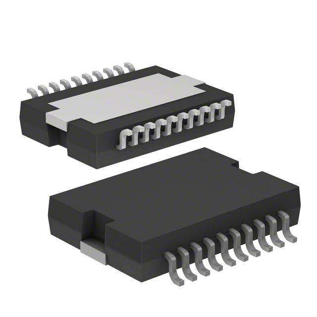
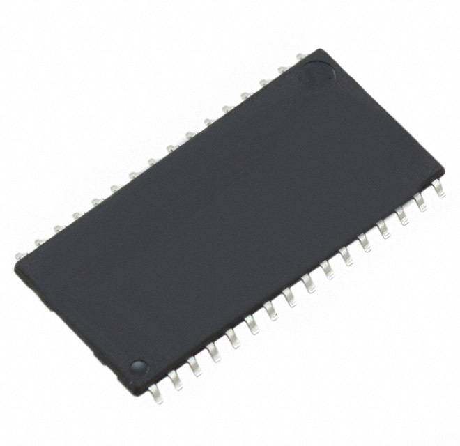
| 描述 | IC CONTROL/LNB SUPPLY 20PWRSOIC专业电源管理 LNB Supply/Cont IC |
| 产品分类 | |
| 品牌 | STMicroelectronics |
| 产品手册 | |
| 产品图片 |
|
| rohs | 符合RoHS无铅 / 符合限制有害物质指令(RoHS)规范要求 |
| 产品系列 | 电源管理 IC,专业电源管理,STMicroelectronics LNBH21PD-TR- |
| 数据手册 | |
| 产品型号 | LNBH21PD-TR |
| 产品目录页面 | |
| 产品种类 | 专业电源管理 |
| 供应商器件封装 | PowerSO-20 |
| 其它名称 | 497-4270-2 |
| 其它有关文件 | http://www.st.com/web/catalog/sense_power/FM142/CL1850/SC1561/PF74989?referrer=70071840 |
| 包装 | 带卷 (TR) |
| 商标 | STMicroelectronics |
| 安装类型 | 表面贴装 |
| 安装风格 | SMD/SMT |
| 封装 | Reel |
| 封装/外壳 | 20-SOIC(0.433",11.00mm 宽)裸焊盘 |
| 封装/箱体 | PowerSO-20 |
| 工作温度 | 0°C ~ 85°C |
| 工作温度范围 | - 40 C to + 125 C |
| 工厂包装数量 | 600 |
| 应用 | 转换器,模拟和数字式卫星信号 STB 接收器/SatTV |
| 标准包装 | 600 |
| 电压-输入 | 8 V ~ 15 V |
| 电压-输出 | 13.3V,18V |
| 类型 | Switching Regulators |
| 系列 | LNBH21 |
| 输出数 | 1 |
| 输出电流 | 750 mA |


PDF Datasheet 数据手册内容提取
LNBH21 LNB SUPPLY AND CONTROL IC WITH 2 STEP-UP CONVERTER AND I C INTERFACE (cid:1) COMPLETEINTERFACEBETWEENLNB ANDI2CTM BUS (cid:1) BUILT-INDC/DCCONTROLLERFOR SINGLE 12VSUPPLYOPERATIONAND HIGHEFFICIENCY(Typ.94%@750mA) (cid:1) TWOSELECTABLEOUTPUTCURRENT LIMIT(450mA/750mA) PowerSO-20 (cid:1) BOTHCOMPLIANTWITHEUTELSATAND DIRECTOUTPUTVOLTAGE SPECIFICATION (cid:1) OVERLOADANDOVER-TEMPERATUREI2C DIAGNOSTICBITs (cid:1) ACCURATEBUILT-IN22KHzTONE (cid:1) LNBSHORTCIRCUITSOA PROTECTION OSCILLATORSUITSWIDELYACCEPTED WITHI2CDIAGNOSTICBIT STANDARDS (cid:1) +/-4KVESDTOLERANTONINPUT/ (cid:1) FASTOSCILLATORSTART-UPFACILITATES DiSEqCTMENCODING OUTPUTPOWERPINS (cid:1) BUILT-IN22KHz TONEDETECTOR DESCRIPTION SUPPORTSBI-DIRECTIONALDiSEqCTM2.0 Intended for analog and digital satellite STB (cid:1) SEMI-LOWDROPPOSTREGULATORAND receivers/SatTV, sets/PC cards, the LNBH21 is a HIGHEFFICIENCYSTEP-UPPWM FOR monolithic voltage regulator and interface IC, LOWPOWERLOSS:Typ.0.56W@125mA assembled in POWER SO-20, specifically (cid:1) TWOOUTPUTPINS SUITABLE TOBYPASS designedtoprovidethe13/18Vpowersupplyand THEOUTPUTR-LFILTERANDAVOIDANY the 22KHz tone signalling to the LNB TONEDISTORSION(R-LFILTERAS PER downconverterintheantennaortothemultiswitch DiSEqC2.0SPECs,seeapplicationcircuiton box. In this application field, it offers a complete pag.5) solutionwithextremely low component count,low (cid:1) CABLE LENGTHDIGITALCOMPENSATION powerdissipationtogetherwithsimpledesignand (cid:1) OVERLOADANDOVER-TEMPERATURE I2CTMstandardinterfacing. INTERNALPROTECTIONS BLOCKDIAGRAM LNBH21 Gate Sense Step-upPWM Vup-Feedback Controller VoTX Vup VoRX Vcc Preregul.+ U.V.lockout +P.ONres. Byp LinearPost-reg ISEL +Modulator +Protections EXTM SDA VSelect Diagnostics SCL I²Cinterf. Enable ADDR DTeotencetor DETIN TEN 22KHz Oscill. DSQIN DSQOUT April2004 1/20
LNBH21 ORDERINGCODES PowerSO-20 PowerSO-20 TYPE (Tube) (Tape&Reel) LNBH21 LNBH21PD LNBH21PD-TR ABSOLUTEMAXIMUMRATINGS Symbol Parameter Value Unit VCC DCInputVoltage -0.3to16 V VUP DCInputVoltage -0.3to25 V IO OutputCurrent InternallyLimited mA VOTX/RX DCOutputPinsVoltage -0.3to25 V VI LogicInputVoltage(SDA,SCL,DSQIN,ISEL) -0.3to7 V VDETIN DetectorInputSignalAmplitude -0.3to2 VPP VOH LogicHighOutputVoltage(DSQOUT) -0.3to7 V IGATE GateCurrent ±400 mA VSENSE CurrentSenseVoltage -0.3to1 V VADDRESS AddressPinVoltage -0.3to7 V Tstg StorageTemperatureRange -40to+150 °C Top OperatingJunctionTemperatureRange -40to+125 °C AbsoluteMaximumRatingsarethosevaluesbeyondwhichdamagetothedevicemayoccur.Functionaloperationundertheseconditionis notimplied. THERMALDATA Symbol Parameter Value Unit Rthj-case ThermalResistanceJunction-case 2 °C/W PINCONFIGUARATION(topview) 2/20
LNBH21 TABLE A:PINCONFIGURATIONS PINN° SYMBOL NAME FUNCTION 18 V SupplyInput 8Vto15VICsupply.A220µFbypasscapacitortoGNDwitha470nF CC (ceramic)inparallelisrecommended 17 GATE ExternalSwitchGate ExternalMOSswitchGateconnectionofthestep-upconverter 16 SENSE CurrentSenseInput DC/DCCurrentSensecomparatorinput.Connectedtocurrent sensingresistor 19 V Step-upVoltage Inputofthelinearpost-regulator.Thevoltageonthispinismonitored UP byinternalstep-utcontrollertokeepaminimumdropoutacrossthe linearpasstransistor 2 V RX OutputPortduring RXOutputtotheLNBinDiSEqC2.0application.Seetruthtablesfor O 22KHzToneRX voltageselectionsonpage8anddescriptiononpage5. 12 SDA SerialData Bidirectionaldatafrom/toI2Cbus. 13 SCL SerialClock ClockfromI2Cbus. 14 DSQIN DiSEqCInput WhentheTENbitoftheSystemRegisterisLOW,thispinwillaccept theDiSEqCcodefromthemainµcontroller.TheLNBH21willusethis codetomodulatetheinternallygenerated22kHzcarrier.SettoGND thispinifnotused. 9 DETIN ToneDetectorInput 22kHzToneDetectorInput.MustbeACcoupledtotheDiSEcQ2.0 bus. 15 DSQOUT DiSEqCOutput OpendrainoutputofthetoneDetectortothemainµcontrollerfor DiSEcQ2.0datadecoding.ItisLOWwhentoneisdetected. 5 EXTM ExternalModulator ExternalModulationInputactsonV TX.NeedsDCdecouplingtothe O ACsource.Ifnotused,canbeleftopen. 1,6,10, GND Ground PinsConnectedtoGround. 11,20 8 BYP BypassCapacitor Neededforinternalpreregulatorfiltering 3 ISEL CurrentLimitSelect SethighorfloatingforIout<=750mA,connecttogroundfor I ≤ 450mA. OUT 4 V TX OutputPortduring Outputofthelinearpost-regulator/modulatortotheLNB.Seetruth O 22KHzToneTX tablesforvoltageselections. 7 ADDR AddressSetting FourI2CbusaddressesavailablebysettingtheAddressPinlevel voltage.Seeaddresspincharacteristicstable. 3/20
LNBH21 TYPICALAPPLICATIONCIRCUITS ApplicationCircuitforDiSEqC1.xandOutputCurrent<450mA DD1111NN44000011 FFeerrrriitteeBBeeaaddFFiilltteerr FMPFMPaa11UUnnRRssaauuAAssggTTooggnnAAeeiiccBBssttLLEEee00XXdd11CCppRREEaaNNrrLL11ttSS--nnAAAAuu6633mm2255bbeerr:: FF11 VVuupp IICC111199 33 IISSEELL CCC222 222222000µµµFFF CC99 IICC22 110000µµFF CC33((******)) 22 VVooRRXX SSeett TTTTXX==11 447700nnFF CCeerraammiicc SSTTSS44DDNNFFSS3300LL ttooLLNNBB 1177 VVooTTXX GGAATTEE 44 LLNNBBHH2211 CC88((******)) DBDB2A2A((TT****44**33)) 1100nnFF LL11==2222µµHH SSEENNSSEE 1166 99 ((****))DDEETTIINN RRsscc 00..11ΩΩΩΩΩΩΩΩ CC44((******)) BByypp 447700nnFF 88 CCeerraammiicc CC55 1188 447700nnFF CC11 VViinn 1122VV 222200µµFF 55 EEXXTTMM SSDDAA 1122 SSCCLL 1133 77 AAddddrreessss 00<<VVAADDDDRR<<VVBBYYPP 1144 GGNNDD 1155 DDSSQQOOUUTT TToonneeEEnnaabbllee DDSSQQIINN((****)) FullApplicationCircuitforBi-directional DiSEqC2.0andOutputCurrentup to750mA FFFF1111ssssuuuuggggggggeeeesssstttteeeeddddppppaaaarrrrttttnnnnuuuummmmbbbbeeeerrrr:::: MPMPMPMPaaaaUUUUnnnnRRRRaaaaAAAAssssTTTTooooAAAAnnnniiiiccccBBBBLLLLEEEE0000XXXX1111CCCCRRRREEEENNNNLLLL1111SSSS----AAAAAAAA6666333322225555 DDD222111NNN444000000111 AAAAxxxxiiiiaaaallllFFFFeeeerrrrrrrriiiitttteeeeBBBBeeeeaaaaddddFFFFiiiilllltttteeeerrrr IIICCC111 FFFllloooaaatttiiinnngggooorrrVVV>>>333...333VVV FFF111 HHHiiiggghhheeerrrcccuuurrrrrreeennntttllliiimmmiiittt VVVuuuppp IIISSSEEELLL CCCC2222 CCC333(((*********))) LLLooowwweeerrrcccuuurrrrrreeennntttllliiimmmiiittt 222222220000µµµµFFFF CCC999 444777000nnnFFF GGGNNNDDD 111000000µµµFFF CCCeeerrraaammmiiiccc VVVoooTTTXXX DDD444(((*********))) DDD111 CCC888(((*********))) BBBAAATTT444333 111NNN555888222111ooorrr 111000000nnnFFF SSSTTTPPPSSS333LLL444000AAA MMMOOOSSS 222777000µµµHHH SSSTTTNNN444NNNFFF000333LLL tttoooLLLNNNBBB GGGaaattteee VVVoooRRRXXX LLLNNNBBBHHH222111 CCC777(((*********))) DBDBDB333AAA(((TTT******444***333))) 111555ooohhhmmm 111000000nnnFFF (((***)))ssseeeeeennnooottteee LLL111===222222µµµHHH SSSeeennnssseee (((******)))DDDEEETTTIIINNN RRRsssccc CCC666 000...000555ΩΩΩΩΩΩΩΩΩΩΩΩ 111000nnnFFF BBByyyppp CCC555 VVVcccccc 444777000nnnFFF CCC111 CCC444(((*********))) VVViiinnn 222222000µµµFFF 444777000nnnFFF 111222VVV CCCeeerrraaammmiiiccc SSSDDDAAA EEEXXXTTTMMM SSSCCCLLL AAADDDDDDRRREEESSSSSS 0000<<<<VVVVAAAADDDDDDDDRRRR<<<<VVVVBBBBYYYYPPPP DDDSSSQQQIIINNN(((******))) GGGNNNDDD DDDSSSQQQOOOUUUTTT 2222KKHHzzTToonneeEEnnaabbllee (*)FiltertobeusedaccordingtoEUTELSATrecommendationtoimplementtheDiSEqCTM2.0,(seeDiSEqCTMimplementationonpage8). IfbidirectionalDiSEqCTM2.0isnotimplementeditcanberemovedbothwithC8andD4. (**)Donotleavethesepinsfloatingifnotused. (***)Tobesolderedascloseaspossibletorelativepins. -C8andD3,4areneededonlytoprotecttheoutputpinsfromanynegativevoltagespikesduringhighspeedvoltagetransitions. 4/20
LNBH21 APPLICATIONINFORMATION This IC has a built in DC/DC step-up controller that, from a single supply source ranging from 8 to 15V, generatesthe voltages (V )that let the linear post-regulatorto work at a minimum dissipated power of UP 1.65W typ. @ 750mA load (the linear regulator drop voltage is internally kept at: V -V =2.2V typ.). An UP O UnderVoltage Lockout circuit will disable the whole circuit when the supplied V drops below a fixed CC threshold (6.7V typically). The internal 22KHz tone generator is factory trimmed in accordance to the standards, andcanbecontrolledeitherbytheI2CTM interfaceorbyadedicatedpin(DSQIN)thatallows immediate DiSEqCTM data encoding (*). When the TEN (Tone ENable) I2C bit it is set to HIGH, a continuous22KHztoneisgeneratedontheoutputregardlessoftheDSQINpinlogicstatus. The TEN bit must be set LOW when the DSQIN pin is used for DiSEqCTM encoding. The fully bi-directional DiSEqCTM 2.0 interfacing is completed by the built-in 22KHz tone detector. Its input pin (DETIN) must be AC coupled to the DiSEqCTM bus, and the extracted PWK data are available on the DSQOUTpin(*). Tocomply tothe bi-directional DiSEqCTM 2.0 bushardware requirementsan output R-Lfilterisneeded. TheLNBH21isprovidedwithtwooutputpins:theV TXtobeusedduringthetonetransmissionandthe O V RXtobeusedwhenthetoneisreceived.Thisallowsthe22KHzTonetopasswithoutanylossesdue O to the R-L filter impedance (see DiSeqC 2.0 application circuit on page 5). In DiSeqC 2.0 applications during the 22KHz transmission activated by DSQIN pin (or TEN I2C bit), the V TX pin must be O preventively set ON by the TTX I2C bit and, both the 13/18V power supply and the 22KHz tone, are providedbymeanofV TXoutput.Assoonasthetonetransmissionisexpired,theV TX mustbesetto O O OFFbysettingtheTTX I2Cbittozeroandthe13/18VpowersupplyisprovidedtotheLNBbytheV RX O pin through the R-L filter. When the LNBH21 is used in DiSeqC 1.x applications the R-L filter is not required (see DiSeqC 1.x application circuit on pag.5), the TTX I2C bit must be kept always to HIGH so that, the V TX output pin can provide both the 13/18V power supply and the 22KHz tone, enabled by O DSQINpinorbyTENI2Cbit. All the functions of this IC are controlled via I2C TM bus bywriting 6 bitson the System Register (SR, 8 bits).Thesameregistercanbereadback,andtwobitswillreportthediagnosticstatus.WhentheICisput in Stand-by (EN bit LOW), the power blocks are disabled. When the regulator blocks are active (EN bit HIGH), the output can be logic controlled to be 13 or18 V bymean of the V bit (Voltage SELect) for SEL remotecontrollingofnon-DiSEqCLNBs. Additionally, the LNBH21 is provided with the LLC I2C bit that increase the selected voltage value (+1V when V =0 and +1.5V when V =1) to compensate for the excess voltage drop along the coaxial SEL SEL cable(LLCbitHIGH). BymeanoftheLLCbit,theLNBH21isalsocomplianttotheAmericanLNBpowersupplystandardsthat requirethehigheroutputvoltagelevelto19.5V(typ.)(insteadof18V),bysimplysettingtheLLC=1when V =1. SEL In order to improve design flexibility and to allow implementation of newcoming LNB remote control standards, an analogic modulation input pin is available (EXTM). An appropriate DC blocking capacitor mustbeusedtocouplethemodulatingsignalsourcetotheEXTMpin.Alsointhiscase,theV TXoutput O mustbesetONduringthetonetransmissionbysettingtheTTXbithigh.Whenexternalmodulationisnot used,therelevantpincanbeleftopen. The current limitation block is SOA type and it is possible to select two current limit thresholds, by the dedicated I pin. The higher threshold is in the range of 750mA to 1A if the I is left floating or SEL SEL connectedavoltage>3.3V.Thelowerthresholdisintherangeof450mAto700mA whentheI pinis SEL connectedtoground.Whentheoutputportisshortedtoground,theSOAcurrentlimitationblocklimitsthe shortcircuitcurrent(I )attypically400mAor200mArespectivelyforV 13Vor18V,toreducethepower SC O dissipation. Moreover, it is possible to set the Short Circuit Current protection either statically (simple currentclamp)ordynamicallybythePCLbitoftheI2CSR;whenthePCL(PulsedCurrentLimiting)bitis settoLOW,theovercurrentprotectioncircuitworksdynamically,assoonasanoverloadisdetected,the outputisshut-downforatimeT , typically900ms. SimultaneouslytheOLF bitoftheSystem Register OFF isset to HIGH. Afterthistimehaselapsed, the output isresumed foratimeT =1/10T (typ.). At the ON OFF endofT ,iftheoverloadisstilldetected,theprotectioncircuitwillcycleagainthroughT andT .At ON OFF ON the end of a full T in which no overload is detected, normal operation is resumed and the OLF bit is ON reset to LOW. Typical T +T time is 990ms and it is determined by an internal timer. This dynamic ON OFF operation can greatly reduce the power dissipation in short circuit condition, still ensuring excellent power-onstartupinmostconditions. 5/20
LNBH21 However,therecouldbesomecasesinwhichanhighlycapacitiveloadontheoutputmaycauseadifficult start-up when the dynamic protection is chosen. This can be solved by initiating any power start-up in staticmode(PCL=HIGH)andthenswitchingtothedynamicmode(PCL=LOW)afterachosenamountof time. When in static mode, the OLF bit goes HIGH when the current clamp limit is reached and returns LOWwhentheoverloadconditioniscleared. This IC is also protected against overheating: when the junction temperature exceeds 150°C (typ.), the step-up converter and the linear regulator are shut off, and the OTF SR bit is set to HIGH. Normal operationisresumedandtheOTFbitisreset toLOWwhenthejunctioniscooleddownto140°C(typ.). (*):Externalcomponentsareneededtocomplytobi-directionalDiSEqCTMbushardwarerequirements.Fullcomplianceofthewholeappli- cationwithDiSEqCTMspecificationsisnotimpliedbytheuseofthisIC I2CBUS INTERFACE Data transmission from main µP to the LNBH21 and viceversa takes place through the 2 wires I2C bus interface, consisting of the two lines SDA and SCL (pull-up resistors to positive supply voltage must be externallyconnected). DATAVALIDITY Asshowninfig.1,thedataontheSDAlinemustbestableduringthehighperiodoftheclock.TheHIGH andLOWstateofthedatalinecanonlychangewhentheclocksignalontheSCLlineisLOW. STARTANDSTOP CONDITIONS As shown in fig.2 a start condition is a HIGH to LOW transition of the SDA line while SCL is HIGH. The stopconditionisaLOW to HIGHtransitionof the SDA line whileSCLisHIGH. A STOP conditions must besent beforeeachSTARTcondition. BYTEFORMAT EverybytetransferredtotheSDAlinemustcontain8bits.Eachbytemustbefollowedbyanacknowledge bit. TheMSB istransferredfirst. ACKNOWLEDGE Themaster(µP)putsaresistiveHIGHlevelontheSDAlineduringtheacknowledgeclockpulse(seefig. 3). The peripheral (LNBH21) that acknowledges has to pull-down (LOW) the SDA line during the acknowledgeclockpulse,sothattheSDAlineisstableLOWduringthisclockpulse.Theperipheralwhich hasbeenaddressedhastogenerateanacknowledgeafterthereceptionofeachbyte,otherwisetheSDA line remains at the HIGH level during the ninth clock pulse time. In this case the master transmitter can generate the STOP information in order to abort the transfer. The LNBH21 won't generate the acknowledgeiftheV supplyisbelowtheUndervoltageLockoutthreshold(6.7Vtyp.). CC TRANSMISSIONWITHOUTACKNOWLEDGE AvoidingtodetecttheacknowledgeoftheLNBH21,theµPcanuseasimplertransmission:simplyitwaits oneclockwithoutcheckingtheslaveacknowledging,andsendsthenewdata. Thisapproachofcourseislessprotectedfrommisworkinganddecreasesthenoiseimmunity. Figure1:DATAVALIDITY ONTHE I2CBUS 6/20
LNBH21 Figure2:TIMINGDIAGRAM ONI2CBUS Figure3:ACKNOWLEDGE ONI2CBUS LNBH21SOFTWARE DESCRIPTION INTERFACEPROTOCOL Theinterfaceprotocolcomprises: -Astartcondition(S) -Achipaddressbyte=hex10/11(theLSBbitdeterminesread(=1)/write(=0)transmission) -Asequenceofdata(1byte+acknowledge) -Astopcondition(P) CHIPADDRESS DATA MSB LSB MSB LSB S 0 0 0 1 0 0 0 R/W ACK ACK P ACK=Acknowledge;S=Start;P=Stop;R/W=Read/Write SYSTEMREGISTER(SR, 1BYTE) MSB LSB R,W R,W R,W R,W R,W R,W R R PCL TTX TEN LLC VSEL EN OTF OLF R,W=readandwritebit;R=Read-onlybit Allbitsresetto0atPower-On 7/20
LNBH21 TRANSMITTEDDATA(I2CBUS WRITE MODE) WhentheR/Wbitinthechipaddressissetto0,themainµPcanwriteontheSystemRegister(SR)ofthe LNBH21viaI2Cbus.Only6bitsoutofthe8availablecanbewrittenbytheµP,sincetheremaining2are left tothediagnosticflags,andareread-only. PCL TTX TEN LLC VSEL EN OTF OLF Function 0 0 1 X X VO=13.25V,VUP=15.25V 0 1 1 X X VO=18V,VUP=20V 1 0 1 X X VO=14.25V,VUP=16.25V 1 1 1 X X VO=19.5V,VUP=21.5V 0 1 X X 22KHziscontrolledbyDSQINpin 1 1 X X 22KHztoneisON,DSQINpindisabled V RXoutputisON,outputvoltagecontrolledbyVSELand 0 1 X X O LLC V TXoutputisON,22KHzcontrolledbyDSQINorTEN, 1 X 1 X X O outputvoltagelevelcontrolledbyVSELandLLC 0 1 X X Pulsed(dynamic)currentlimitingisselected 1 1 X X Staticcurrentlimitingisselected X X X X X 0 X X Powerblocksdisabled X=don'tcare. Valuesaretypicalunlessotherwisespecified RECEIVEDDATA(I2CbusREADMODE) TheLNBH21canprovidetotheMasteracopyoftheSYSTEMREGISTERinformationviaI2Cbusinread mode. The read mode is Master activated by sending the chip address with R/W bit set to 1. At the following master generated clocks bits, the LNBH21 issues a byte on the SDA data bus line (MSB transmittedfirst). AttheninthclockbittheMCUmastercan: -acknowledgethereception,startinginthiswaythetransmissionof anotherbytefrom theLNBH21; -noacknowledge,stoppingthereadmodecommunication. While the whole register is read back by the µP, only the two read-only bits OLF and OTF convey diagnosticinformationsabout theLNBH21. Valuesaretypicalunlessotherwisespecified. PCL TTX TEN LLC VSEL EN OTF OLF Function 0 TJ<140°C,normaloperation Thesebitsarereadexactlythesameas 1 TJ>150°C,powerblockdisabled theywereleftafterlastwriteoperation 0 IOUT<IOMAX,normaloperation 1 IOUT>IOMAX,overloadprotectiontriggered Valuesaretypicalunlessotherwisespecified POWER-ONI2CINTERFACERESET TheI2CinterfacebuiltintheLNBH21isautomaticallyresetatpower-on.Aslongas theV staysbelow CC the UnderVoltage Lockout threshold (6.7V typ.), the interface will not respond to any I2C command and the System Register (SR) is initialized to all zeroes, thus keeping the power blocks disabled. Once the V risesabove7.3Vtyp,theI2CinterfacebecomesoperativeandtheSRcanbeconfiguredbythemain CC µP. This is due to 500mV of hysteresis provided in the UVL threshold to avoid false retriggering of the Power-Onreset circuit. ADDRESS PIN ConnectingthispintoGNDtheChipI2Cinterfaceaddressis0001000,but,itispossibletochoiceamong 4differentaddresses simplysettingthispinat 4fixedvoltagelevels(seetableonpage10). 8/20
LNBH21 DiSEqCTMIMPLEMENTATION TheLNBH21helpsthesystemdesignertoimplementthebi-directional(2.0)DiSEqCprotocolbyallowing aneasyPWKmodulation/demodulationofthe22KHzcarrier.ThePWKdataareexchangedbetweenthe LNBH21 and the main µP using logic levels that are compatible with both 3.3 and 5V microcontrollers. This data exchange is madethrough twodedicatedpins, DSQINand DSQOUT, inorderto maintain the timingrelationshipsbetweenthePWKdataandthePWKmodulationasaccurateaspossible.Thesetwo pinsshouldbedirectlyconnectedtotwoI/OpinsoftheµP,thusleavingtotheresidentfirmwarethetask of encoding and decoding the PWK data in accordance to the DiSEqC protocol. Full compliance of the systemtothespecificationisthusnotimpliedbythebareuseoftheLNBH21.Thesystemdesignershould also take in consideration the bus hardware requirements; that can be simply accomplished by the R-L terminationconnectedontheV pinsoftheLNBH21,asshownintheTypicalApplicationCircuitonpage O 4. To avoid any losses due to the R-L impedance during the tone transmission, the LNBH21 has dedicated output (V TX) that, in a DiSEqC 2.0 application, is connected after the filter and must be O enabled by setting the TTX SR bit HIGH only during the tone transmission (see DiSEqC 2.O operation descriptiononpage2). Unidirectional(1.x)DiSEqCandnon-DiSEqCsystemsnormallydon'tneedthistermination,andtheV TX O pincan be directlyconnected tothe LNB supplyport of the Tuner(see DiSeqC 1.x applicationcircuit on pag.4).ThereisalsononeedofToneDecoding,thusDETINandDSQOUTpinscanbeleftunconnected andtheToneisprovidedby theV TX. O 9/20
LNBH21 ELECTRICALCHARACTERISTICSFORLNBPSERIES(T =0to85°C,EN=1,TTX=0/1,DSQIN=LOW, J LLC=TEN=PCL=VSEL=0,V =12V,I =50mA, unlessotherwisespecified.Seesoftwaredescription IN O sectionforI2Caccesstothesystemregister). Symbol Parameter TestConditions Min. Typ. Max. Unit V SupplyVoltage I =750mA TEN=VSEL=LLC=1 8 15 V IN O I SupplyCurrent EN=TEN=VSEL=LLC=1,NOLOAD 20 40 mA I EN=0 3.5 7 V OutputVoltage I =750mA VSEL=1 LLC=0 17.3 18 18.7 V O O LLC=1 18.7 19.5 20.3 V OutputVoltage I =750mA VSEL=0 LLC=0 12.75 13.25 13.75 V O O LLC=1 13.75 14.25 14.75 ∆V LineRegulation V =8to15V VSEL=0 5 40 mV O IN1 VSEL=1 5 60 ∆V LoadRegulation VSEL=0or1,I =50to750mA 200 mV O O I OutputCurrentLimiting ISEL=FloatingorV>3.3V 750 1000 mA MAX ISEL=GND 450 700 I OutputShortCircuitCurrent VSEL=0 300 mA SC VSEL=1 200 t DynamicOverload PCL=0 OutputShorted 900 ms OFF protectionOFFTime t DynamicOverload PCL=0 OutputShorted t /10 ms ON OFF protectionONTime f ToneFrequency TEN=1 20 22 24 KHz TONE A ToneAmplitude TEN=1 0.55 0.72 0.9 V TONE PP D ToneDutyCycle TEN=1 40 50 60 % TONE t,t ToneRiseandFallTime TEN=1 5 8 15 µs r f G ExternalModulationGain ∆V /∆V , f=10Hzto50KHz 6 EXTM OUT EXTM V ExternalInputVoltage ACCoupling 400 mV EXTM PP Z ExternalModulation f=10Hzto50KHz 260 Ω EXTM Impedance f DC/DCConverterSwitching 220 kHz SW Frequency f ToneDetectorFrequency 0.4Vppsinewave 18 24 kHz DETIN CaptureRange V ToneDetectorInput f =22kHzsinewave 0.2 1.5 V DETIN IN PP Amplitude Z ToneDetectorInput 150 kΩ DETIN Impedance V DSQOUTPinLogicLOW Tonepresent I =2mA 0.3 0.5 V OL OL I DSQOUTPinLeakage Toneabsent V =6V 10 µA OZ OH Current V DSQINInputPinLogic 0.8 V IL LOW V DSQINInputPinLogic 2 V IH HIGH I DSQINPinsInputCurrent V =5V 15 µA IH IH I OutputBackwardCurrent EN=0, V =18V -6 -15 mA OBK OBK T TemperatureShutdown 150 °C SHDN Threshold ∆T TemperatureShutdown 15 °C SHDN Hysteresis 10/20
LNBH21 GATE ANDSENSEELECTRICALCHARACTERISTICS(T =0to85°C,V =12V) J IN Symbol Parameter TestConditions Min. Typ. Max. Unit R GateLOWR I =-100mA 4.5 Ω DSON-L DSON GATE R GateHIGHR I =100mA 4.5 Ω DSON-H DSON GATE V CurrentLimitSenseVoltage 200 mV SENSE I2CELECTRICALCHARACTERISTICS(T =0to85°C,V =12V) J I Symbol Parameter TestConditions Min. Typ. Max. Unit V LOWLevelInputVoltage SDA,SCL 0.8 V IL V HIGHLevelInputVoltage SDA,SCL 2 V IH I InputCurrent SDA,SCL,V =0.4to4.5V -10 10 µA I I V LowLevelOutputVoltage SDA(opendrain),I =6mA 0.6 V OL OL f MaximumClockFrequency SCL 500 KHz MAX ADDRESS PINCHARACTERISTICS(T =0to85°C,V =12V) J IN Symbol Parameter TestConditions Min. Typ. Max. Unit V "0001000"AddrPinVoltage 0 0.7 V ADDR-1 V "0001001"AddrPinVoltage 1.3 1.7 V ADDR-2 V "0001010"AddrPinVoltage 2.3 2.7 V ADDR-3 V "0001011"AddrPinVoltage 3.3 5 V ADDR-4 11/20
LNBH21 THERMALDESIGNNOTES During normal operation, the LNBH21 device dissipates some power. At maximum rated output current (750mA), thevoltagedrop onthelinearregulatorlead toa total dissipatedpowerthatistypically1.65W. The heat generated requires a suitable heatsink to keep the junction temperature below the over temperature protection threshold. Assuming a 45°C temperature inside the Set-Top-Box case, the total R hastobelessthan48°C/W. thj-amb While this can be easily achieved using a through-hole power package that can be attached to a small heatsink or to the metallic frame of the receiver, a surface mount power package must rely on PCB solutions whose thermal efficiency is often limited. The simplest solution is to use a large, continuous copperareaof theGNDlayertodissipatetheheatcomingfromtheICbody. Given an R equal to 2°C/W, a maximum of 46°C/W are left to the PCB heatsink. This figure is thj-case achievedifaminimumof6.5cm2copperareaisplacedjustbelowtheICbody.Thisareacanbetheinner GNDlayerofamulti-layerPCB,or,inaduallayerPCB,anunbrokenGNDareaevenontheoppositeside where the IC is placed. In figure 4, it is shown a suggested layout for the PSO-20 package with a dual layer PCB, where the IC exposed pad connected to GND and the square dissipating area are thermally connectedthrough32viasholes,filledbysolder.Thisarrangement,whenL=25mm,achievesanR thc-amb ofabout32°C/W. Different layouts are possible, too. Basic principles, however, suggest to keep the IC and its ground exposedpadapproximatelyinthemiddleofthedissipatingarea;toprovideasmanyviasaspossible;to design a dissipating area having a shape as square as possible and not interrupted by other copper traces. Figure4:PowerSO-20SUGGESTEDPCB HEATSINK LAYOUT 12/20
LNBH21 TYPICALCHARACTERISTICS(unlessotherwisespecifiedT =25°C) j Figure5:OutputVoltagevsTemperature Figure8:LoadRegulationvsTemperature Figure6:OutputVoltagevsTemperature Figure9:LoadRegulationvsTemperature Figure7:OutputVoltagevsTemperature Figure10:SupplyCurrentvsTemperature 13/20
LNBH21 Figure11:SupplyCurrentvsTemperature Figure14:DynamicOverloadProtectionOFF TimevsTemperature Figure12:SupplyCurrentvsTemperature Figure15:OutputCurrent Limitingvs Temperature Figure13:DynamicOverloadProtectionON Figure16:OutputCurrent Limitingvs TimevsTemperature Temperature 14/20
LNBH21 Figure17:ToneFrequencyvsTemperature Figure20:ToneRiseTimevsTemperature Figure18:ToneAmplitudevsTemperature Figure21:ToneFallTimevsTemperature Figure19:ToneDutyCyclevsTemperature Figure22:UndervoltageLockoutThresholdvs Temperature 15/20
LNBH21 Figure23:OutputBackwardCurrentvs Figure26:22kHzToneWaveform Temperature V =12V,I =50mA,EN=TEN=1 CC O Figure24:DC/DCConverterEfficiencyvs Figure27:DSQINToneEnableTransient Temperature Response V =12V,I =50mA,EN=1,ToneenabledbyDSQINPin CC O Figure25:CurrentLimit SenseVoltagevs Figure28:DSQINToneEnableTransient Temperature Response VCC=12V,IO=50mA,EN=1,ToneenabledbyDSQINPin 16/20
LNBH21 Figure29:DSQINToneDisableTransient Response V =12V,I =50mA,EN=1,ToneenabledbyDSQINPin CC O 17/20
LNBH21 PowerSO-20 MECHANICAL DATA mm. inch DIM. MIN. TYP MAX. MIN. TYP. MAX. A 3.60 0.1417 a1 0.10 0.30 0.0039 0.0118 a2 3.30 0.1299 a3 0 0.10 0 0.0039 b 0.40 0.53 0.0157 0.0209 c 0.23 0.32 0.0090 0.0013 D (1) 15.80 16.00 0.6220 0.630 E 13.90 14.50 0.5472 0.5710 e 1.27 0.0500 e3 11.43 0.4500 E1 (1) 10.90 11.10 0.4291 0.4370 E2 2.90 0.1141 G 0 0.10 0.0000 0.0039 h 1.10 0.0433 L 0.80 1.10 0.0314 0.0433 N 10˚ 10˚ S 0˚ 8˚ 0˚ 8˚ T 10.0 0.3937 (1) “D and E1” do not include mold flash or protusions - Mold flash or protusions shall not exceed 0.15mm (0.006”) N N R a2 A c a1 b e DETAILB DETAILA E e3 D DETAILA leda 20 11 slug a3 DETAILB E2 E1 0.35 T Gage Plaen -C- S L SEATINGPLANE G C (COPLANARITY) 1 1 0 PSO20MEC hx45˚ 0056635 18/20
LNBH21 Tape & Reel PowerSO-20 MECHANICAL DATA mm. inch DIM. MIN. TYP MAX. MIN. TYP. MAX. A 330 12.992 C 12.8 13.2 0.504 0.519 D 20.2 0.795 N 60 2.362 T 30.4 1.197 Ao 15.1 15.3 0.594 0.602 Bo 16.5 16.7 0.650 0.658 Ko 3.8 4.0 0.149 0.157 Po 3.9 4.1 0.153 0.161 P 23.9 24.1 0.941 0.949 W 23.7 24.3 0.933 0.957 19/20
LNBH21 Information furnished is believed to be accurate and reliable. However, STMicroelectronics assumes no responsibility for the consequences of use of such information nor for any infringement of patents or other rights of third parties which may result from its use. No license is granted by implication or otherwise under any patent or patent rights of STMicroelectronics. Specifications mentioned in this publication are subject to change without notice. This publication supersedes and replaces all information previously supplied. STMicroelectronics products are not authorized for use as critical components in life support devices or systems without express written approval of STMicroelectronics. The ST logo is a registered trademark of STMicroelectronics All other names are the property of their respective owners © 2004 STMicroelectronics - All Rights Reserved STMicroelectronics GROUP OF COMPANIES Australia - Belgium - Brazil - Canada - China - Czech Republic - Finland - France - Germany - Hong Kong - India - Israel - Italy - Japan - Malaysia - Malta - Morocco - Singapore - Spain - Sweden - Switzerland - United Kingdom - United States. http://www.st.com 20/20