ICGOO在线商城 > LMZ12002EXTTZ/NOPB

 Datasheet下载
- 型号: LMZ12002EXTTZ/NOPB
- 制造商: Texas Instruments
- 库位|库存: xxxx|xxxx
- 要求:
| 数量阶梯 | 香港交货 | 国内含税 |
| +xxxx | $xxxx | ¥xxxx |
查看当月历史价格
查看今年历史价格
LMZ12002EXTTZ/NOPB产品简介:
ICGOO电子元器件商城为您提供LMZ12002EXTTZ/NOPB由Texas Instruments设计生产,在icgoo商城现货销售,并且可以通过原厂、代理商等渠道进行代购。 提供LMZ12002EXTTZ/NOPB价格参考以及Texas InstrumentsLMZ12002EXTTZ/NOPB封装/规格参数等产品信息。 你可以下载LMZ12002EXTTZ/NOPB参考资料、Datasheet数据手册功能说明书, 资料中有LMZ12002EXTTZ/NOPB详细功能的应用电路图电压和使用方法及教程。
| 参数 | 数值 |
| 产品目录 | |
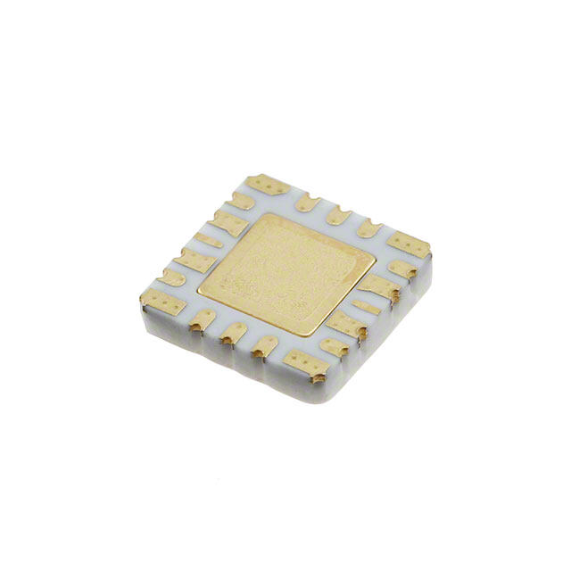
| 描述 | IC BUCK SYNC ADJ 2A TO-PMOD-7稳压器—开关式稳压器 2A Pwr Mod |
| 产品分类 | DC DC Converters集成电路 - IC |
| 品牌 | Texas Instruments |
| 产品手册 | http://www.ti.com/litv/snvs662f |
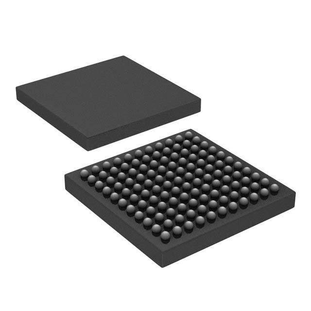
| 产品图片 |
|
| rohs | 符合RoHS无铅 / 符合限制有害物质指令(RoHS)规范要求 |
| 产品系列 | 电源管理 IC,稳压器—开关式稳压器,Texas Instruments LMZ12002EXTTZ/NOPBSIMPLE SWITCHER® |
| 数据手册 | |
| 产品型号 | LMZ12002EXTTZ/NOPB |
| 产品培训模块 | http://www.digikey.cn/PTM/IndividualPTM.page?site=cn&lang=zhs&ptm=30148 |
| 产品种类 | 稳压器—开关式稳压器 |
| 其它名称 | LMZ12002EXTTZ/NOPBDKR |
| 制造商产品页 | http://www.ti.com/general/docs/suppproductinfo.tsp?distId=10&orderablePartNumber=LMZ12002EXTTZ/NOPB |
| 功率(W)-制造系列 | 12W |
| 功率(W)-最大值 | 12W |
| 包装 | Digi-Reel® |
| 商标 | Texas Instruments |
| 商标名 | SIMPLE SWITCHER |
| 大小/尺寸 | 0.40" 长 x 0.54" 宽 x 0.18" 高(10.2mm x 13.8mm x 4.6mm) |
| 安装类型 | 表面贴装 |
| 安装风格 | SMD/SMT |
| 宽度 | 13.8 mm |
| 封装 | Reel |
| 封装/外壳 | TO-PMOD-7,电源模块 |
| 封装/箱体 | TO-PMOD-7 |
| 工作温度 | -55°C ~ 125°C |
| 工作温度范围 | - 55 C to + 125 C |
| 工厂包装数量 | 250 |
| 开关频率 | 1 MHz |
| 效率 | 92% |
| 最大输入电压 | 20 V |
| 标准包装 | 1 |
| 特性 | 带有 UVLO |
| 电压-输入(最大值) | 20V |
| 电压-输入(最小值) | 4.5V |
| 电压-输出1 | 0.8 ~ 6 V |
| 电压-输出2 | - |
| 电压-输出3 | - |
| 电压-隔离 | - |
| 电流-输出(最大值) | 2A |
| 类型 | Voltage Converter |
| 系列 | LMZ12002EXT |
| 视频文件 | http://www.digikey.cn/classic/video.aspx?PlayerID=1364138032001&width=640&height=455&videoID=1041965290001 |
| 设计资源 | http://www.digikey.com/product-highlights/cn/zh/texas-instruments-webench-design-center/3176 |
| 输入电压 | 4.5 VDC to 20 VDC |
| 输出数 | 1 |
| 输出电压 | 800 mV to 6 V |
| 输出电流 | 2 A |
| 输出端数量 | 1 Output |
| 配用 | /product-detail/zh/LMZ12002EXTEVAL%2FNOPB/LMZ12002EXTEVAL%2FNOPB-ND/2399075 |


PDF Datasheet 数据手册内容提取
Product Sample & Technical Tools & Support & Folder Buy Documents Software Community LMZ12002EXT SNVS662G–JUNE2010–REVISEDAUGUST2015 ® LMZ12002EXT 2-A SIMPLE SWITCHER Power Module With 20-V Maximum Input Voltage for Demanding Environments and Rugged Applications 1 Features 2 Applications • JunctionTemperatureRange–55°Cto125°C • Point-of-loadConversionsfrom5-Vand12-V 1 • IntegratedShieldedInductor InputRail • SimplePCBLayout • Time-CriticalProjects • FlexibleStart-upSequencingUsingExternalSoft- • Space-ConstrainedHighThermalRequirement StartCapacitorandPrecisionEnable Applications • ProtectionAgainstInrushCurrentsandFaults • NegativeOutputVoltageApplications(SeeAN- SuchasInputUVLOandOutputShortCircuit 2027SNVA425) • SingleExposedPadandStandardPinoutforEasy 3 Description MountingandManufacturing The LMZ12002EXT SIMPLE SWITCHER® power • FastTransientResponseforFPGAsandASICs module is an easy-to-use step-down DC-DC solution • LowOutputVoltageRipple capable of driving up to 2-A load with exceptional • Pin-to-PinCompatibleWithFamilyDevices: power conversion efficiency, line and load regulation, and output accuracy. The LMZ12002EXT is available – LMZ14203EXT/2EXT/1EXT(42-VMaximum3 in an innovative package that enhances thermal A,2A,1A) performance and allows for hand or machine – LMZ14203/2/1(42-VMaximum3A,2A,1A) soldering. – LMZ12003/2/1(20-VMaximum3A,2A,1A) The LMZ12002EXT can accept an input voltage rail • FullyWEBENCH®PowerDesignerenabled between 4.5 V and 20 V, and can deliver an • LowRadiatedEmissionsandHighRadiated adjustable and highly accurate output voltage as low Immunity as 0.8 V. The LMZ12002EXT only requires three external resistors and four external capacitors to • PassesVibrationStandardMIL-STD-883Method complete the power solution. The LMZ12002EXT is a 2007.2ConditionAJESD22–B103BCondition1 reliable and robust design with the following • PassesDropStandardMIL-STD-883Method protection features: thermal shutdown, input 2002.3ConditionBJESD22–B110ConditionB undervoltage lockout, output overvoltage protection, short-circuit protection, output current limit, and the • ElectricalSpecifications device allows start-up into a prebiased output. A – 12-WMaximumTotalPowerOutput single resistor adjusts the switching frequency up to 1 – Upto2-AOutputCurrent MHz. – InputVoltageRange4.5Vto20V DeviceInformation(1)(2) – OutputVoltageRange0.8Vto6V PARTNUMBER PACKAGE BODYSIZE(NOM) – Efficiencyupto92% LMZ12002EXT NDW(7) 10.16mm×9.85mm (1) For all available packages, see the orderable addendum at theendofthedatasheet. (2) Peak reflow temperature equals 245°C. See SNAA214 for moredetails. SimplifiedApplicationSchematic Efficiency5-VInputat25°C 100 LMZ12002EXT 95 VIN VIN RON EN GND SS FB VOUT 8950 VOUT @ 2A Y (%) 80 11..85 RON CFF ENC 75 1.2 Enable RFBT EFFICI 6750 60 CIN CSS RFBB COUT 55 25°C 50 0 0.4 0.8 1.2 1.6 2 OUTPUT CURRENT (A) 1 An IMPORTANT NOTICE at the end of this data sheet addresses availability, warranty, changes, use in safety-critical applications, intellectualpropertymattersandotherimportantdisclaimers.PRODUCTIONDATA.
LMZ12002EXT SNVS662G–JUNE2010–REVISEDAUGUST2015 www.ti.com Table of Contents 1 Features.................................................................. 1 8 ApplicationandImplementation........................ 14 2 Applications........................................................... 1 8.1 ApplicationInformation............................................14 3 Description............................................................. 1 8.2 TypicalApplication .................................................14 4 RevisionHistory..................................................... 2 9 PowerSupplyRecommendations...................... 20 5 PinConfigurationandFunctions......................... 3 10 Layout................................................................... 20 6 Specifications......................................................... 3 10.1 LayoutGuidelines.................................................20 6.1 AbsoluteMaximumRatings......................................3 10.2 LayoutExamples...................................................21 6.2 ESDRatings..............................................................3 10.3 PowerDissipationandThermalConsiderations...22 6.3 RecommendedOperatingConditions.......................4 10.4 PowerModuleSMTGuidelines............................22 6.4 ThermalInformation..................................................4 11 DeviceandDocumentationSupport................. 24 6.5 ElectricalCharacteristics...........................................4 11.1 DeviceSupport......................................................24 6.6 TypicalCharacteristics .............................................6 11.2 DocumentationSupport........................................24 7 DetailedDescription............................................ 12 11.3 CommunityResources..........................................24 7.1 Overview.................................................................12 11.4 Trademarks...........................................................24 7.2 FunctionalBlockDiagram.......................................12 11.5 ElectrostaticDischargeCaution............................24 7.3 FeatureDescription.................................................12 11.6 Glossary................................................................24 7.4 DeviceFunctionalModes........................................13 12 Mechanical,Packaging,andOrderable Information........................................................... 25 4 Revision History NOTE:Pagenumbersforpreviousrevisionsmaydifferfrompagenumbersinthecurrentversion. ChangesfromRevisionF(October2013)toRevisionG Page • AddedESDRatingstable,FeatureDescriptionsection,DeviceFunctionalModes,ApplicationandImplementation section,PowerSupplyRecommendationssection,Layoutsection,DeviceandDocumentationSupportsection,and Mechanical,Packaging,andOrderableInformationsection. ................................................................................................ 1 ChangesfromRevisionE(April2013)toRevisionF Page • Deleted12mils....................................................................................................................................................................... 4 • Changed10mils................................................................................................................................................................... 20 • Changed10mils................................................................................................................................................................... 22 • ChangedPowerModuleSMTGuidelines............................................................................................................................ 22 2 SubmitDocumentationFeedback Copyright©2010–2015,TexasInstrumentsIncorporated ProductFolderLinks:LMZ12002EXT
LMZ12002EXT www.ti.com SNVS662G–JUNE2010–REVISEDAUGUST2015 5 Pin Configuration and Functions NDWPackage 7-Pin TopView PinFunctions PIN TYPE DESCRIPTION NAME NO. Enable—Inputtotheprecisionenablecomparator.Risingthresholdis1.18-Vnominal;90- EN 3 Analog mVhysteresisnominal.Maximumrecommendedinputlevelis6.5V. ExposedPad—Internallyconnectedtopin4.Usedtodissipateheatfromthepackage EP — Ground duringoperation.Mustbeelectricallyconnectedtopin4externaltothepackage. Feedback—Internallyconnectedtotheregulation,over-voltage,andshort-circuit FB 6 Analog comparators.Theregulationreferencepointis0.8Vatthisinputpin.Connectedthe feedbackresistordividerbetweentheoutputandgroundtosettheoutputvoltage. GND 4 Ground Ground—Referencepointforallstatedvoltages.MustbeexternallyconnectedtoEP. ON-TimeResistor—AnexternalresistorfromV tothispinsetstheON-timeofthe RON 2 Analog IN application.Typicalvaluesrangefrom25kΩto124kΩ. Soft-Start—Aninternal8-µAcurrentsourcechargesanexternalcapacitortoproducethe SS 5 Analog soft-startfunction.Thisnodeisdischargedat200-µAduringdisable,overcurrent,thermal shutdownandinternalUVLOconditions. Supplyinput—Nominaloperatingrangeis4.5Vto20V.Asmallamountofinternal VIN 1 Power capacitanceiscontainedwithinthepackageassembly.Additionalexternalinputcapacitance isrequiredbetweenthispinandexposedpad. OutputVoltage—Outputfromtheinternalinductor.Connecttheoutputcapacitorbetween VOUT 7 Power thispinandexposedpad. 6 Specifications 6.1 Absolute Maximum Ratings(1) MIN MAX UNIT VIN,RONtoGND –0.3 25 V EN,FB,SStoGND –0.3 7 V JunctionTemperature 150 °C StorageTemperatureRange –65 150 °C PeakReflowCaseTemperature(30sec) 245 °C (1) StressesbeyondthoselistedunderAbsoluteMaximumRatingsmaycausepermanentdamagetothedevice.Thesearestressratings only,whichdonotimplyfunctionaloperationofthedeviceattheseoranyotherconditionsbeyondthoseindicatedunderRecommended OperatingConditions.Exposuretoabsolute-maximum-ratedconditionsforextendedperiodsmayaffectdevicereliability. 6.2 ESD Ratings VALUE UNIT V Electrostaticdischarge Humanbodymodel(HBM),perANSI/ESDA/JEDECJS-001(1)(2) ±2000 V (ESD) (1) JEDECdocumentJEP155statesthat500-VHBMallowssafemanufacturingwithastandardESDcontrolprocess.Manufacturingwith lessthan500-VHBMispossiblewiththenecessaryprecautions. (2) Thehumanbodymodelisa100-pFcapacitordischargedthrougha1.5-kΩresistorintoeachpin.TestmethodisperJESD-22-114. Copyright©2010–2015,TexasInstrumentsIncorporated SubmitDocumentationFeedback 3 ProductFolderLinks:LMZ12002EXT
LMZ12002EXT SNVS662G–JUNE2010–REVISEDAUGUST2015 www.ti.com 6.3 Recommended Operating Conditions overoperatingfree-airtemperaturerange(unlessotherwisenoted) MIN MAX UNIT V 4.5 20 V IN EN 0 6.5 V OperationJunctionTemperature –55 125 °C 6.4 Thermal Information LMZ12002EXT THERMALMETRIC(1) NDW UNIT 7PINS R 4-layerJEDECPrinted-Circuit-Board,100 θJA 19.3 °C/W vias,Noairflow Junction-to-ambientthermalresistance(2) 2-layerJEDECPrinted-Circuit-Board,No 21.5 °C/W airflow R Junction-to-case(top)thermalresistance Noairflow 1.9 °C/W θJC(top) (1) Formoreinformationabouttraditionalandnewthermalmetrics,seetheSemiconductorandICPackageThermalMetricsapplication report,SPRA953. (2) R measuredona1.705-in×3.0-in4-layerboard,with1-oz.copper,thirtyfivethermalvias,noairflow,and1-Wpowerdissipation. θJA RefertoPCBlayoutdiagrams 6.5 Electrical Characteristics LimitsareforT =25°Cunlessotherwisespecified.MinimumandMaximumlimitsareensuredthroughtest,designor J statisticalcorrelation.TypicalvaluesrepresentthemostlikelyparametricnormatT =25°C,andareprovidedforreference J purposesonly.Unlessotherwisestatedthefollowingconditionsapply:V =12V,V =1.8V. IN OUT PARAMETER TESTCONDITIONS MIN(1) TYP(2) MAX(1) UNIT SYSTEMPARAMETERS ENABLECONTROL 1.18 VEN ENthresholdtrippoint VENrising overthejunctiontemperature V 1.1 1.26 (T)rangeof–55°Cto+125°C J V ENthresholdhysteresis V falling 90 mV EN-HYS EN SOFT-START 8 ISS SSsourcecurrent VSS=0V overthejunctiontemperature µA 4.9 11 (T)rangeof–55°Cto+125°C J I SSdischargecurrent –200 µA SS-DIS CURRENTLIMIT 2.6 ICL Currentlimitthreshold DCaverage overthejunctiontemperature A 2.3 3.65 (T)rangeof–55°Cto+125°C J ON/OFFTIMER ONtimerminimumpulse t 150 ns ON-MIN width t OFFtimerpulsewidth 260 ns OFF (1) MinandMaxlimitsare100%productiontestedat25°C.Limitsovertheoperatingtemperaturerangeareensuredthroughcorrelation usingStatisticalQualityControl(SQC)methods.LimitsareusedtocalculateTexasInstruments'AverageOutgoingQualityLevel (AOQL). (2) Typicalnumbersareat25°Candrepresentthemostlikelyparametricnormal. 4 SubmitDocumentationFeedback Copyright©2010–2015,TexasInstrumentsIncorporated ProductFolderLinks:LMZ12002EXT
LMZ12002EXT www.ti.com SNVS662G–JUNE2010–REVISEDAUGUST2015 Electrical Characteristics (continued) LimitsareforT =25°Cunlessotherwisespecified.MinimumandMaximumlimitsareensuredthroughtest,designor J statisticalcorrelation.TypicalvaluesrepresentthemostlikelyparametricnormatT =25°C,andareprovidedforreference J purposesonly.Unlessotherwisestatedthefollowingconditionsapply:V =12V,V =1.8V. IN OUT PARAMETER TESTCONDITIONS MIN(1) TYP(2) MAX(1) UNIT REGULATIONANDOVERVOLTAGECOMPARATOR V >+0.8V 0.795 SS TJ=–55°Cto125°C overthejunctiontemperature V V In-regulationfeedback IO=2A (TJ)rangeof–55°Cto+125°C 0.775 0.815 FB voltage V >+0.8V SS T =25°C 0.784 0.8 0.816 J I =10mA O Feedbackovervoltage V 0.92 V FB-OV protectionthreshold Feedbackinputbias I 5 nA FB current Non-switchinginput I V =0.86V 1 mA Q current FB Shutdownquiescent I V =0V 25 μA SD current EN THERMALCHARACTERISTICS T Thermalshutdown Rising 165 °C SD Thermalshutdown T Falling 15 °C SD-HYST hysteresis PERFORMANCEPARAMETERS(3) ΔV Outputvoltageripple 8 mV O PP ΔV /ΔV Lineregulation V =8Vto20V,I =2A 0.01% O IN IN O ΔV /ΔV Loadregulation V =12V 1.5 mV/A O IN IN V =12V,V =1.8V,I =1A 87% IN O O η Efficiency V =12V,V =1.8V,I =2A 77% IN O O (3) EN55022:2006,+A1:2007,FCCPart15SubpartB:2007.SeeAN-2024andlayoutforinformationondeviceundertest. Copyright©2010–2015,TexasInstrumentsIncorporated SubmitDocumentationFeedback 5 ProductFolderLinks:LMZ12002EXT
LMZ12002EXT SNVS662G–JUNE2010–REVISEDAUGUST2015 www.ti.com 6.6 Typical Characteristics Unlessotherwisespecified,thefollowingconditionsapply:V =12V;C =10-µFX7RCeramic;C =100-µFX7RCeramic; IN IN O T =25°Cforefficiencycurvesandwaveforms. A 100 1.2 95 1.8 90 1.0 1.5 %) 85 W) 0.8 ENCY ( 7850 111...825 ATION ( 0.6 1.2 FICI 70 SSIP EF 65 DI 0.4 60 0.2 55 25°C 25°C 50 0 0 0.4 0.8 1.2 1.6 2 0 0.4 0.8 1.2 1.6 2 OUTPUT CURRENT (A) OUTPUT CURRENT (A) Figure1.Efficiency4.5-VInputat25°C Figure2.Dissipation4.5-VInputat25°C 100 1.2 95 1.8 1.0 90 1.5 Y (%) 8805 11..85 ON (W) 0.8 ENC 75 1.2 ATI 0.6 1.2 FICI 70 SSIP EF 65 DI 0.4 60 0.2 55 25°C 25°C 50 0 0 0.4 0.8 1.2 1.6 2 0 0.4 0.8 1.2 1.6 2 OUTPUT CURRENT (A) OUTPUT CURRENT (A) Figure3.Efficiency5-VInputat25°C Figure4.Dissipation5-VInputat25°C 100 1.2 95 2.5 1.0 1.8 90 1.5 Y (%) 8805 112...855 ON (W) 0.8 NC 75 1.2 TI 0.6 E A FICI 70 SSIP 1.2 EF 65 DI 0.4 60 0.2 55 25°C 25°C 50 0 0 0.4 0.8 1.2 1.6 2 0 0.4 0.8 1.2 1.6 2 OUTPUT CURRENT (A) OUTPUT CURRENT (A) Figure5.Efficiency6-VInputat25°C Figure6.Dissipation6-VInputat25°C 6 SubmitDocumentationFeedback Copyright©2010–2015,TexasInstrumentsIncorporated ProductFolderLinks:LMZ12002EXT
LMZ12002EXT www.ti.com SNVS662G–JUNE2010–REVISEDAUGUST2015 Typical Characteristics (continued) Unlessotherwisespecified,thefollowingconditionsapply:V =12V;C =10-µFX7RCeramic;C =100-µFX7RCeramic; IN IN O T =25°Cforefficiencycurvesandwaveforms. A 100 1.2 95 5.0 90 5.0 1.0 3.3 3.3 Y (%) 8805 112...855 ON (W) 0.8 12..85 ENC 75 1.2 ATI 0.6 1.5 FICI 70 SSIP 1.2 EF 65 DI 0.4 60 0.2 25°C 55 25°C 50 0 0 0.4 0.8 1.2 1.6 2 0 0.4 0.8 1.2 1.6 2 OUTPUT CURRENT (A) OUTPUT CURRENT (A) Figure7.Efficiency8-VInputat25°C Figure8.Dissipation6-VInputat25°C 100 1.2 6.0 95 6.0 5.0 1.0 90 5.0 3.3 3.3 NCY (%) 788505 1112....8255 TION (W) 00..68 12..85 E A 1.5 FICI 70 SSIP 1.2 EF 65 DI 0.4 60 0.2 55 25°C 25°C 50 0 0 0.4 0.8 1.2 1.6 2 0 0.4 0.8 1.2 1.6 2 OUTPUT CURRENT (A) OUTPUT CURRENT (A) Figure9.Efficiency12-VInputat25°C Figure10.Dissipation12-VInputat25°C 100 1.8 95 6.0 1.5 90 5.0 6.0 NCY (%) 788505 123...853 TION (W) 01..92 2.5 35..30 FICIE 70 SSIPA 1.8 EF 65 DI 0.6 60 0.3 55 25°C 25°C 50 0 0 0.4 0.8 1.2 1.6 2 0 0.4 0.8 1.2 1.6 2 OUTPUT CURRENT (A) OUTPUT CURRENT (A) Figure11.Efficiency20-VInputat25°C Figure12.Dissipation20-VInputat25°C Copyright©2010–2015,TexasInstrumentsIncorporated SubmitDocumentationFeedback 7 ProductFolderLinks:LMZ12002EXT
LMZ12002EXT SNVS662G–JUNE2010–REVISEDAUGUST2015 www.ti.com Typical Characteristics (continued) Unlessotherwisespecified,thefollowingconditionsapply:V =12V;C =10-µFX7RCeramic;C =100-µFX7RCeramic; IN IN O T =25°Cforefficiencycurvesandwaveforms. A 100 1.6 1.8 1.4 90 1.2 CY (%) 80 1.8 )W( NO 1.0 1.5 N 1.2 IT 0.8 E A CI P 1.2 EFFI 70 1.5 ISSID 0.6 0.4 60 0.2 85°C 85°C 50 0.0 0 0.4 0.8 1.2 1.6 2 0 0.4 0.8 1.2 1.6 2.0 OUTPUT CURRENT (A) OUTPUT CURRENT (A) Figure13.Efficiency4.5-VInputat85°C Figure14.Dissipation4.5-VInputat85°C 100 1.4 1.2 90 1.2 %) 1.8 )W 1.0 CY ( 80 ( NO 0.8 EN 1.2 ITA 1.5 CI P 0.6 EFFI 70 1.5 ISSID 0.4 1.8 60 0.2 85°C 85°C 50 0.0 0 0.4 0.8 1.2 1.6 2 0 0.4 0.8 1.2 1.6 2 OUTPUT CURRENT (A) OUTPUT CURRENT (A) Figure15.Efficiency5-VInputat85°C Figure16.Dissipation5-VInputat85°C 100 1.4 1.2 2.5 90 %) 2.5 )W 1.0 1.8 CY ( 80 1.8 ( NO 0.8 1.2 N IT E A CI 1.2 P 0.6 FFI 70 1.5 ISS 1.5 E ID 0.4 60 0.2 85°C 85°C 50 0.0 0 0.4 0.8 1.2 1.6 2 0 0.4 0.8 1.2 1.6 2 OUTPUT CURRENT (A) OUTPUT CURRENT (A) Figure17.Efficiency6-VInputat85°C Figure18.Dissipation6-VInputat85°C 8 SubmitDocumentationFeedback Copyright©2010–2015,TexasInstrumentsIncorporated ProductFolderLinks:LMZ12002EXT
LMZ12002EXT www.ti.com SNVS662G–JUNE2010–REVISEDAUGUST2015 Typical Characteristics (continued) Unlessotherwisespecified,thefollowingconditionsapply:V =12V;C =10-µFX7RCeramic;C =100-µFX7RCeramic; IN IN O T =25°Cforefficiencycurvesandwaveforms. A 100 1.6 5.0 3.3 2.5 1.4 1.5 90 1.2 1.8 CY (%) 80 )W( NO 1.0 3.32.5 N 1.8 IT 0.8 E A FFICI 70 1.5 1.2 PISS 0.6 5.0 1.2 E ID 0.4 60 85°C 0.2 85°C 50 0.0 0 0.4 0.8 1.2 1.6 2 0 0.4 0.8 1.2 1.6 2.0 OUTPUT CURRENT (A) OUTPUT CURRENT (A) Figure19.Efficiency8-VInputat85°C Figure20.Dissipation8-VInputat85°C 100 1.6 5.0 6.0 3.3 1.4 3.3 90 1.2 2.5 %) )W CY ( 80 ( NO 1.0 5.0 N IT 0.8 E A FFICI 70 2.5 1.8 1.2 PISS 0.6 6.0 1.2 E 1.5 ID 0.4 60 1.5 1.8 0.2 85°C 85°C 50 0.0 0 0.4 0.8 1.2 1.6 2 0 0.4 0.8 1.2 1.6 2.0 OUTPUT CURRENT (A) OUTPUT CURRENT (A) Figure21.Efficiency12-VInputat85°C Figure22.Dissipation12-VInputat85°C 100 1.6 6.0 1.4 6.0 90 3.3 1.2 %) 5.0 )W 1.8 CY ( 80 2.5 ( NO 1.0 2.5 N 1.8 IT 0.8 5.0 E A FFICI 70 3.3 PISS 0.6 E ID 0.4 60 0.2 85°C 85°C 50 0.0 0 0.4 0.8 1.2 1.6 2 0 0.4 0.8 1.2 1.6 2.0 OUTPUT CURRENT (A) OUTPUT CURRENT (A) Figure23.Efficiency20-VInputat85°C Figure24.Dissipation20-VInputat85°C Copyright©2010–2015,TexasInstrumentsIncorporated SubmitDocumentationFeedback 9 ProductFolderLinks:LMZ12002EXT
LMZ12002EXT SNVS662G–JUNE2010–REVISEDAUGUST2015 www.ti.com Typical Characteristics (continued) Unlessotherwisespecified,thefollowingconditionsapply:V =12V;C =10-µFX7RCeramic;C =100-µFX7RCeramic; IN IN O T =25°Cforefficiencycurvesandwaveforms. A 1.820 1.825 1.820 1.814 OUTPUT VOLTAGE (V)111...788900628 620 8 541.52 )V( EGATLOV TUPTUO11111.....788889001150505 12 4.5 68 25°C 1.790 20 5 85°C 1.790 1.785 0 0.4 0.8 1.2 1.6 2 0 0.4 0.8 1.2 1.6 2 OUTPUT CURRENT (A) OUTPUT CURRENT (A) Figure25.LineandLoadRegulationat25°C Figure26.LineandLoadRegulationat85°C 1.825 1.820 V) 1.815 E ( G A 1.810 T L VO 1.805 6 T 8 PU 1.800 12 5 T 4.5 OU 1.795 20 1.790 -55°C 2200 mmVV//dDiivv 1.00 Ps/Div 1.785 0 0.4 0.8 1.2 1.6 2 12V 3.3V 2A20mV/div1μs/div IN O OUTPUT CURRENT (A) Figure27.LineandLoadRegulationat–55°C Figure28.OutputRipple 3.5 3.3 50 mV/Div T (A) N E 3.1 R R SHORT CIRCUIT U C T 2.9 U P T U ONSET O 2.7 25°C 0.5 A/Div 200 Ps/Div 2.5 12V 3.3V 0.6-Ato2-AStep 0 5 10 15 20 25 IN O INPUT VOLTAGE (V) Figure29.TransientResponse Figure30.CurrentLimit1.8VOUTat25°C 10 SubmitDocumentationFeedback Copyright©2010–2015,TexasInstrumentsIncorporated ProductFolderLinks:LMZ12002EXT
LMZ12002EXT www.ti.com SNVS662G–JUNE2010–REVISEDAUGUST2015 Typical Characteristics (continued) Unlessotherwisespecified,thefollowingconditionsapply:V =12V;C =10-µFX7RCeramic;C =100-µFX7RCeramic; IN IN O T =25°Cforefficiencycurvesandwaveforms. A 3.5 3.5 3.3 3.3 OUTPUT CURRENT (A) 232...917 SHORTO CNISRECTUIT OUTPUT CURRENT (A) 223...791 SHOORNTS CEITRCUIT 25°C 85°C 2.5 2.5 0 5 10 15 20 25 0 5 10 15 20 25 INPUT VOLTAGE (V) INPUT VOLTAGE (V) Figure31.CurrentLimit3.3VOUTat25°C Figure32.CurrentLimit1.8VOUTat85°C 3.5 3.3 A) T ( N E 3.1 R R U C PUT 2.9 SHORT CIRCUIT T U O 2.7 -55°C ONSET 2.5 0 5 10 15 20 25 INPUT VOLTAGE (V) Figure33.CurrentLimit1.8VOUTat–55°C Figure34.ThermalDeratingVOUT=1.8V Copyright©2010–2015,TexasInstrumentsIncorporated SubmitDocumentationFeedback 11 ProductFolderLinks:LMZ12002EXT
LMZ12002EXT SNVS662G–JUNE2010–REVISEDAUGUST2015 www.ti.com 7 Detailed Description 7.1 Overview TheLMZ12002EXTpowermoduleisaneasy-to-usestep-downDC-DCsolutioncapableofdrivingupto2-Aload withexceptionalpowerconversionefficiency,lineandloadregulation,andoutputaccuracy. 7.2 Functional Block Diagram Vin VIN 1 5 Linear reg Cvcc CIN SS Css 3 T EN S 0.47 éF B C RON 2 RON VOUT 7 Timer VO CFF 6.8 éH Co 6 FB RFBT Internal RFBB Regulator IC Passives GND 4 7.3 Feature Description 7.3.1 COTControlCircuitOverview Constant ON-Time control is based on a comparator and an ON-time one-shot, with the output voltage feedback compared with an internal 0.8-V reference. If the feedback voltage is below the reference, the main MOSFET is turned on for a fixed ON-time determined by a programming resistor R . R is connected to V such that ON- ON ON IN time is reduced with increasing input supply voltage. Following this ON-time, the main MOSFET remains off for a minimum of 260 ns. If the voltage on the feedback pin falls below the reference level again the ON-time cycle is repeated.Regulationisachievedinthismanner. 7.3.2 OutputOvervoltageComparator The voltage at FB is compared to a 0.92-V internal reference. If FB rises above 0.92 V the ON-time is immediately terminated. This condition is known as overvoltage protection (OVP). It can occur if the input voltage is increased very suddenly or if the output load is decreased very suddenly. Once OVP is activated, the top MOSFET ON-times will be inhibited until the condition clears. Additionally, the synchronous MOSFET will remain onuntilinductorcurrentfallstozero. 7.3.3 CurrentLimit Current limit detection is carried out during the OFF-time by monitoring the current in the synchronous MOSFET. Referring to the Functional Block Diagram, when the top MOSFET is turned off, the inductor current flows through the load, the PGND pin and the internal synchronous MOSFET. If this current exceeds 2.85 A (typical) thecurrentlimitcomparatordisablesthestartofthenextON-timeperiod.Thenextswitchingcyclewilloccuronly if the FB input is less than 0.8 V and the inductor current has decreased below 2.85 A. Inductor current is monitored during the period of time the synchronous MOSFET is conducting. So long as inductor current exceeds 2.85 A, further ON-time intervals for the top MOSFET will not occur. Switching frequency is lower during currentlimitduetothelongerOFF-time. NOTE Current limit is dependent on both duty cycle and temperature as illustrated in the graphs intheTypicalCharacteristicssection. 12 SubmitDocumentationFeedback Copyright©2010–2015,TexasInstrumentsIncorporated ProductFolderLinks:LMZ12002EXT
LMZ12002EXT www.ti.com SNVS662G–JUNE2010–REVISEDAUGUST2015 Feature Description (continued) 7.3.4 ThermalProtection The junction temperature of the LMZ12002EXT must not be allowed to exceed its maximum ratings. Thermal protection is implemented by an internal Thermal Shutdown circuit which activates at 165°C (typical) causing the device to enter a low power standby state. In this state the main MOSFET remains off causing V to fall, and O additionally the CSS capacitor is discharged to ground. Thermal protection helps prevent catastrophic failures for accidental device overheating. When the junction temperature falls back below 145°C (typical hysteresis = 20°C) theSSpinisreleased,V risessmoothly,andnormaloperationresumes. O Applications requiring maximum output current especially those at high input voltage may require application deratingatelevatedtemperatures. 7.3.5 ZeroCoilCurrentDetection The current of the lower (synchronous) MOSFET is monitored by a zero coil current detection circuit which inhibits the synchronous MOSFET when its current reaches zero until the next ON-time. This circuit enables the DCMoperatingmode,whichimprovesefficiencyatlightloads. 7.3.6 PrebiasedStart-Up TheLMZ12002EXTwillproperlystartupintoaprebiasedoutput.Thisstart-upsituationiscommoninmultiplerail logic applications where current paths may exist between different power rails during the start-up sequence. The followingscopecaptureshowsproperbehaviorduringthisevent. Figure35. PrebiasedStart-Up 7.4 Device Functional Modes 7.4.1 DiscontinuousConductionandContinuousConductionModes At light load the regulator will operate in discontinuous conduction mode (DCM). With load currents above the critical conduction point, it will operate in continuous conduction mode (CCM). When operating in DCM the switching cycle begins at zero amps inductor current; increases up to a peak value, and then recedes back to zero before the end of the OFF-time. Note that during the period of time that inductor current is zero, all load current is supplied by the output capacitor. The next ON-time period starts when the voltage on the at the FB pin falls below the internal reference. The switching frequency is lower in DCM and varies more with load current as compared to CCM. Conversion efficiency in DCM is maintained because conduction and switching losses are reducedwiththesmallerloadandlowerswitchingfrequency. Copyright©2010–2015,TexasInstrumentsIncorporated SubmitDocumentationFeedback 13 ProductFolderLinks:LMZ12002EXT
LMZ12002EXT SNVS662G–JUNE2010–REVISEDAUGUST2015 www.ti.com 8 Application and Implementation NOTE Information in the following applications sections is not part of the TI component specification, and TI does not warrant its accuracy or completeness. TI’s customers are responsible for determining suitability of components for their purposes. Customers should validateandtesttheirdesignimplementationtoconfirmsystemfunctionality. 8.1 Application Information TheLMZ12002EXTisastep-downDC-to-DCpowermodule.ItistypicallyusedtoconvertahigherDCvoltageto a lower DC voltage with a maximum output current of 2 A. The following design procedure can be used to select components for the LMZ12002EXT. Alternately, the WEBENCH software may be used to generate complete designs. When generating a design, the WEBENCH software uses iterative design procedure and accesses comprehensivedatabasesofcomponents.Pleasegotowww.ti.com formoredetails 8.2 Typical Application U1 EP Enable VIN LMZ12002EXTTZ-ADJ T VIN RON EN GND SS FB VOU 1.8VO @ 2A 1 2 3 4 5 6 7 4.5V to 20V R32E.N4Tk CFF RON 0.022 PF 32.4k RFBT 1.37k R11E.N8Bk C10IN P2F 1C IPNF1 0.022C PSFS R1.F0B7Bk 1C OPF1 1C0O02 PF Figure36. EvaluationBoardSchematicDiagram 8.2.1 DesignRequirements Forthisexamplethefollowingapplicationparametersexist. • V Range=Upto20V IN • V =0.8Vto6V OUT • I =2A OUT 14 SubmitDocumentationFeedback Copyright©2010–2015,TexasInstrumentsIncorporated ProductFolderLinks:LMZ12002EXT
LMZ12002EXT www.ti.com SNVS662G–JUNE2010–REVISEDAUGUST2015 Typical Application (continued) 8.2.2 DetailedDesignProcedure TheLMZ12002EXTisfullysupportedbyWEBENCHandoffersthefollowing:componentselection,electricaland thermal simulations as well as the build-it board for a reduction in design time. The following list of steps can be usedtomanuallydesigntheLMZ12002EXTapplication. 1. SelectminimumoperatingV withenabledividerresistors IN 2. ProgramV withdividerresistorselection O 3. Programturnontimewithsoft-startcapacitorselection 4. SelectC O 5. SelectC IN 6. SetoperatingfrequencywithR ON 8.2.2.1 EnableDivider,R andR Selection ENT ENB The enable input provides a precise 1.18-V band-gap rising threshold to allow direct logic drive or connection to a voltage divider from a higher enable voltage such as Vin. The enable input also incorporates 90 mV (typical) of hysteresisresultinginafallingthresholdof1.09V.ThemaximumrecommendedvoltageintotheENpinis6.5V. For applications where the midpoint of the enable divider exceeds 6.5 V, a small Zener diode can be added to limitthisvoltage. The function of this resistive divider is to allow the designer to choose an input voltage below which the circuit will be disabled. This implements the feature of programmable under voltage lockout. This is often used in battery powered systems to prevent deep discharge of the system battery. It is also useful in system designs for sequencing of output rails or to prevent early turnon of the supply as the main input voltage rail rises at power- up. Applying the enable divider to the main input rail is often done in the case of higher input voltage systems where a lower boundary of operation must be established. In the case of sequencing supplies, the divider is connected to a rail that becomes active earlier in the power-up cycle than the LMZ12002EXT output rail. The two resistorsmustbechosenbasedonthefollowingratio: R /R =(V /1.18V)–1 (1) ENT ENB INUVLO The LMZ12002EXT demonstration and evaluation boards use 11.8 kΩ for R and 32.4 kΩ for R resulting in ENB ENT arisingUVLOof4.5V.Thisdividerpresents5.34VtotheENinputwhenthedividerinputisraisedto20V. 8.2.2.2 OutputVoltageSelection Output voltage is determined by a divider of two resistors connected between V and ground. The midpoint of O the divider is connected to the FB input. The voltage at FB is compared to a 0.8-V internal reference. In normal operation an ON-time cycle is initiated when the voltage on the FB pin falls below 0.8 V. The main MOSFET ON- time cycle causes the output voltage to rise and the voltage at the FB to exceed 0.8 V. As long as the voltage at FBisabove0.8V,ON-timecycleswillnotoccur. TheregulatedoutputvoltagedeterminedbytheexternaldividerresistorsRFBTandRFBBis: V =0.8V×(1+R /R ) (2) O FBT FBB Rearrangingterms;theratioofthefeedbackresistorsforadesiredoutputvoltageis: R /R =(V /0.8V)–1 (3) FBT FBB O Theseresistorsmustbechosenfromvaluesintherangeof1.0kΩ to10.0kΩ. For V = 0.8 V the FB pin can be connected to the output directly so long as an output preload resistor remains O that draws more than 20 µA. Converter operation requires this minimum load to create a small inductor ripple currentandmaintainproperregulationwhennoloadispresent. A feed-forward capacitor is placed in parallel with R to improve load step transient response. Its value is FBT usually determined experimentally by load stepping between DCM and CCM conduction modes and adjusting for besttransientresponseandminimumoutputripple. Table1liststhevaluesforR ,R ,C andR . FBT FBB FF ON Copyright©2010–2015,TexasInstrumentsIncorporated SubmitDocumentationFeedback 15 ProductFolderLinks:LMZ12002EXT
LMZ12002EXT SNVS662G–JUNE2010–REVISEDAUGUST2015 www.ti.com Typical Application (continued) Table1.BillofMaterials REFDES DESCRIPTION CASESIZE MANUFACTURER MANUFACTURERP/N U1 SIMPLESWITCHER PFM-7 TexasInstruments LMZ12002EXTTZ-ADJ C 1µF,50V,X7R 1206 TaiyoYuden UMK316B7105KL-T in1 C 10µF,50V,X7R 1210 TaiyoYuden UMK325BJ106MM-T in2 C 1µF,50V,X7R 1206 TaiyoYuden UMK316B7105KL-T O1 C 100µF,6.3V,X7R 1210 TaiyoYuden JMK325BJ10CR7MM-T O2 R 1.37kΩ 0603 VishayDale CRCW06031K37FKEA FBT R 1.07kΩ 0603 VishayDale CRCW06031K07FKEA FBB R 32.4kΩ 0603 VishayDale CRCW060332K4FKEA ON R 32.4kΩ 0603 VishayDale CRCW060332K4FKEA ENT R 11.8kΩ 0603 VishayDale CRCW060311k8FKEA ENB C 22nF,±10%,X7R,16V 0603 TDK C1608X7R1H223K FF C 22nF,±10%,X7R,16V 0603 TDK C1608X7R1H223K SS 8.2.2.3 Soft-StartCapacitorSelection Programmable soft-start permits the regulator to slowly ramp to its steady-state operating point after being enabled, thereby reducing current inrush from the input supply and slowing the output voltage rise-time to preventovershoot. Upon turnon, after all UVLO conditions have been passed, an internal 8-µA current source begins charging the externalsoft-startcapacitor.Thesoft-starttimedurationtoreachsteadystateoperationisgivenbytheformula: t =V ×C /Iss=0.8V×C /8µA (4) SS REF SS SS Thisequationcanberearrangedasfollows: C =t ×8μA/0.8V (5) SS SS Useofa0.022-μFcapacitorresultsin2.2-mssoft-startduration.Thisisrecommendedasaminimumvalue. As the soft-start input exceeds 0.8 V the output of the power stage will be in regulation. The soft-start capacitor continues charging until it reaches approximately 3.8 V on the SS pin. Voltage levels between 0.8 V and 3.8 V have no effect on other circuit operation. The following conditions will reset the soft-start capacitor by discharging theSSinputtogroundwithaninternal200-μAcurrentsink. • Theenableinputbeingpulledlow • Thermalshutdowncondition • Overcurrentfault • InternalV UVLO(Approx4-VinputtoV ) CC IN 8.2.2.4 C Selection O None of the required C output capacitance is contained within the module. At a minimum, the output capacitor O must meet the worst case minimum ripple current rating of 0.5 × I , as calculated in Equation 17 below. LR P-P Beyond that, additional capacitance will reduce output ripple so long as the ESR is low enough to permit it. A minimum value of 10 μF is generally required. Experimentation will be required if attempting to operate with a minimumvalue.CeramiccapacitorsorotherlowESRtypesarerecommended.SeeAN-2024formoredetail. ThefollowingequationprovidesagoodfirstpassapproximationofC forloadtransientrequirements: O C ≥I ×V ×L×V /(4×V ×(V –V )×V ) (6) O STEP FB IN O IN O OUT-TRAN Solving: C ≥2A×0.8V×10μH×12V/(4×3.3V×(12V–3.3V)×33mV) O ≥50μF The LMZ12002EXT demonstration and evaluation boards are populated with a 100-µF 6.3-V X5R output capacitor.Locationsforextraoutputcapacitorsareprovided.SeeAN-2024forlocations. 16 SubmitDocumentationFeedback Copyright©2010–2015,TexasInstrumentsIncorporated ProductFolderLinks:LMZ12002EXT
LMZ12002EXT www.ti.com SNVS662G–JUNE2010–REVISEDAUGUST2015 8.2.2.5 C Selection IN The LMZ12002EXT module contains an internal 0.47-µF input ceramic capacitor. Additional input capacitance is required external to the module to handle the input ripple current of the application. This input capacitance must belocatedinverycloseproximitytothemodule.Inputcapacitorselectionisgenerallydirectedtosatisfytheinput ripple current requirements rather than by capacitance value. Worst case input ripple current rating is dictated by theequation: I(C )≊1/2×I ×√(D/1-D) IN(RMS) O where • D≊V /V (7) O IN As a point of reference, the worst case ripple current will occur when the module is presented with full load currentandwhenV =2 ×V . IN O Recommended minimum input capacitance is 10-µF X7R ceramic with a voltage rating at least 25% higher than the maximum applied input voltage for the application. It is also recommended that attention be paid to the voltageandtemperaturederatingsofthecapacitorselected. NOTE Ripple current rating of ceramic capacitors may be missing from the capacitor data sheet andyoumayhavetocontactthecapacitormanufacturerforthisrating. If the system design requires a certain minimum value of input ripple voltage ΔV be maintained then the IN followingequationmaybeused. C ≥I ×D×(1–D)/f ×ΔV (8) IN O SW-CCM IN IfΔV is1%ofV fora20-Vinputto3.3-Voutputapplicationthisequals200mVandf =400kHz. IN IN SW C ≥2A×3.3V/20V×(1–3.3V/20V)/(400000×0.200V) IN ≥3.4μF (9) Additional bulk capacitance with higher ESR may be required to damp any resonant effects of the input capacitanceandparasiticinductanceoftheincomingsupplylines. 8.2.2.6 R ResistorSelection ON Many designs will begin with a desired switching frequency in mind. For that purpose the following equation can beused. f ≊V /(1.3×10-10×R ) (10) SW(CCM) O ON Thiscanberearrangedas R ≊V /(1.3×10-10×f ) (11) ON O SW(CCM) The selection of RON and f must be confined by limitations in the ON-time and OFF-time for the COT SW(CCM) ControlCircuitOverviewsection. The ON-time of the LMZ12002EXT timer is determined by the resistor R and the input voltage V . It is ON IN calculatedasfollows: t =(1.3×10⁻¹⁰×R )/V (12) ON ON IN Theinverserelationshipoft andV givesanearlyconstantswitchingfrequencyasVINisvaried.R mustbe ON IN ON selected such that the ON-time at maximum V is greater than 150 ns. The ON-timer has a limiter to ensure a IN minimum of 150 ns for t . This limits the maximum operating frequency, which is governed by the following ON equation: f =V /(V ×150ns) (13) SW(MAX) O IN(MAX) This equation can be used to select R if a certain operating frequency is desired so long as the minimum ON- ON timeof150nsisobserved.ThelimitforR canbecalculatedasfollows: ON R ≥V ×150ns/(1.3×10-10) (14) ON IN(MAX) If R calculated in Equation 11 is less than the minimum value determined in Equation 14 a lower frequency ON mustbeselected.Alternatively,V canalsobelimitedinordertokeepthefrequencyunchanged. IN(MAX) Copyright©2010–2015,TexasInstrumentsIncorporated SubmitDocumentationFeedback 17 ProductFolderLinks:LMZ12002EXT
LMZ12002EXT SNVS662G–JUNE2010–REVISEDAUGUST2015 www.ti.com Additionally, consider the minimum OFF-time of 260 ns limits the maximum duty ratio. Larger R (lower F ) ON SW mustbeselectedinanyapplicationrequiringlargedutyratio. 8.2.2.7 DiscontinuousConductionandContinuousConductionModesSelection OperatingfrequencyinDCMcanbecalculatedasfollows: f ≊V ×(V –1)×10μH×1.18×1020×I /(V –V )×R 2 (15) SW(DCM) O IN O IN O ON In CCM, current flows through the inductor through the entire switching cycle and never falls to zero during the OFF-time. The switching frequency remains relatively constant with load current and line voltage variations. The CCMoperatingfrequencycanbecalculatedusingEquation10above. Figure37isacomparisonpairofwaveformsoftheshowingbothCCM(upper)andDCMoperatingmodes. V =12V,V =3.3V,I =2A/0.26A2μs/div IN O O Figure37. CCMandDCMOperatingModes TheapproximateformulafordeterminingtheDCM/CCMboundaryisasfollows: I ≊V ×(V –V )/(2×10μH×f ×V ) (16) DCB O IN O SW(CCM) IN Figure38isatypicalwaveformshowingtheboundarycondition. V =12V,V =3.3V,I =0.29A2μs/div IN O O Figure38. TransitionModeOperation The inductor internal to the module is 10 μH. This value was chosen as a good balance between low and high input voltage applications. The main parameter affected by the inductor is the amplitude of the inductor ripple current(I ).I canbecalculatedwith: LR LR I =V ×(V –V )/(10µH×f ×V ) LRP-P O IN O SW IN where • V isthemaximuminputvoltage IN • andf isdeterminedfromEquation10. (17) SW If the output current I is determined by assuming that I = I , the higher and lower peak of I can be O O L LR determined.BeawarethatthelowerpeakofI mustbepositiveifCCMoperationisrequired. LR 18 SubmitDocumentationFeedback Copyright©2010–2015,TexasInstrumentsIncorporated ProductFolderLinks:LMZ12002EXT
LMZ12002EXT www.ti.com SNVS662G–JUNE2010–REVISEDAUGUST2015 8.2.3 ApplicationCurves 100 2.5 95 90 2 %) 85 T (A) Y ( 80 EN1.5 C R EFFICIEN 677505 UTPUT CUR 1 O 60 0.5 55 25°C 50 0 0 0.5 1 1.5 2 50 60 70 80 90 100 110 120 OUTPUT CURRENT (A) AMBIENT TEMPERATURE (°C) VIN=12V,VOUT=5V VIN=12V,VOUT=5V Figure39.Efficiency Figure40.ThermalDeratingCurve 80.0 m) 70.0 V/ BP 60.0 d NS ( 50.0 SSIO40.0 EN 55022 CLASS B LIMIT MI D E30.0 E AT 20.0 DI RA 10.0 0.0 0 200 400 600 800 1000 FREQUENCY (MHz) Figure41.RadiatedEmissions(EN55022ClassB)fromEvaluationBoard Copyright©2010–2015,TexasInstrumentsIncorporated SubmitDocumentationFeedback 19 ProductFolderLinks:LMZ12002EXT
LMZ12002EXT SNVS662G–JUNE2010–REVISEDAUGUST2015 www.ti.com 9 Power Supply Recommendations The LMZ12002EXT device is designed to operate from an input voltage supply range between 4.5 V and 20 V. This input supply must be well regulated and able to withstand maximum input current and maintain a stable voltage.Theresistanceoftheinputsupplyrailmustbelowenoughthataninputcurrenttransientdoesnotcause a high enough drop at the LMZ12002EXT supply voltage that can cause a false UVLO fault triggering and system reset. If the input supply is more than a few inches from the LMZ12002EXT, additional bulk capacitance may be required in addition to the ceramic bypass capacitors. The amount of bulk capacitance is not critical, but a47-μFor100-μFelectrolyticcapacitorisatypicalchoice. 10 Layout 10.1 Layout Guidelines PCB layout is an important part of DC-DC converter design. Poor board layout can disrupt the performance of a DC-DC converter and surrounding circuitry by contributing to EMI, ground bounce and resistive voltage drop in the traces. These can send erroneous signals to the DC-DC converter resulting in poor regulation or instability. Goodlayoutcanbeimplementedbyfollowingafewsimpledesignrules. 1. Minimizeareaofswitchedcurrentloops. FromanEMIreductionstandpoint,itisimperativetominimizethehighdi/dtcurrentpathsduringPCBlayout. The high current loops that do not overlap have high di/dt content that will cause observable high frequency noiseontheoutputpiniftheinputcapacitorC isplacedadistanceawayfortheLMZ12002EXT.Therefore IN1 physically place C asa close as possible to the LMZ12002EXT VIN and GND exposed pad. This will IN1 minimize the high di/dt area and reduce radiated EMI. Additionally, grounding for both the input and output capacitormustconsistofalocalizedtopsideplanethatconnectstotheGNDexposedpad(EP). 2. Haveasinglepointground. The ground connections for the feedback, soft-start, and enable components must be routed to the GND pin of the device. This prevents any switched or load currents from flowing in the analog ground traces. If not properly handled, poor grounding can result in degraded load regulation or erratic output voltage ripple behavior.Providethesinglepointgroundconnectionfrompin4toEP. 3. MinimizetracelengthtotheFBpin. Both feedback resistors, R and R , and the feed forward capacitor C , must be located close to the FB FBT FBB FF pin. Because the FB node is high impedance, maintain the copper area as small as possible. The trace are fromR ,R ,andC mustberoutedawayfromthebodyoftheLMZ12002EXTtominimizenoise. FBT FBB FF 4. Makeinputandoutputbusconnectionsaswideaspossible. This reduces any voltage drops on the input or output of the converter and maximizes efficiency. To optimize voltageaccuracyattheload,ensurethataseparatefeedbackvoltagesensetraceismadetotheload.Doing sowillcorrectforvoltagedropsandprovideoptimumoutputaccuracy. 5. Provideadequatedeviceheat-sinking. Use an array of heat-sinking vias to connect the exposed pad to the ground plane on the bottom PCB layer. If the PCB has a plurality of copper layers, these thermal vias can also be employed to make connection to inner layer heat-spreading ground planes. For best results use a 6 × 6 via array with minimum via diameter of 8 mils thermal vias spaced 59 mils (1.5 mm). Ensure enough copper area is used for heat-sinking to keep thejunctiontemperaturebelow125°C. 20 SubmitDocumentationFeedback Copyright©2010–2015,TexasInstrumentsIncorporated ProductFolderLinks:LMZ12002EXT
LMZ12002EXT www.ti.com SNVS662G–JUNE2010–REVISEDAUGUST2015 10.2 Layout Examples VIN LMZ12002EXT VO VIN VOUT High Cin1 di/dt CO1 GND Loop 1 Loop 2 Figure42. CriticalCurrentLoopstoMinimize Top View Thermal Vias GND GND EPAD CIN 1 2 3 4 5 6 7 COUT VIN VIN RONEN GNDSS FBVOUT VOUT RON RENT CSS RFBT CFF RENB RFBB GND Plane Figure43. PCBLayoutGuide Figure44. TopViewofEvaluationPCB Copyright©2010–2015,TexasInstrumentsIncorporated SubmitDocumentationFeedback 21 ProductFolderLinks:LMZ12002EXT
LMZ12002EXT SNVS662G–JUNE2010–REVISEDAUGUST2015 www.ti.com Layout Examples (continued) Figure45. BottomViewofEvaluationPCB 10.3 Power Dissipation and Thermal Considerations For the design case of V = 12 V, V = 3.3 V, I = 2 A, T = 85°C, and T = 125°C, the device IN O O AMB(MAX) JUNCTION mustseeathermalresistancefromcasetoambientof: R <(T –T )/P –R (18) θCA J-MAX AMB(MAX) IC-LOSS θJC Given the typical thermal resistance from junction to case to be 1.9°C/W .Use the 85°C power dissipation curves in the Typical Characteristics section to estimate the P for the application being designed. In this IC-LOSS applicationitis1.2W R <(125–85)/1.2W–1.9=31.4 θCA To reach R = 31.4, the PCB is required to dissipate heat effectively. With no airflow and no external heat, a θCA goodestimateoftherequiredboardareacoveredby1-oz.copperonboththetopandbottommetallayersis: BoardArea_cm2=500°C×cm2/W/R (19) θJC As a result, approximately 15.9 square cm of 1-oz. copper on top and bottom layers is required for the PCB design. The PCB copper heat sink must be connected to the exposed pad. Approximately thirty six, 8 mils thermal vias spaced 59 mils (1.5 mm) apart must connect the top copper to the bottom copper. For an example ofahighthermalperformancePCBlayout,refertothedemoboardapplicationnoteAN-2024SNVA422. 10.4 Power Module SMT Guidelines Therecommendationsbelowareforastandardmodulesurfacemountassembly • LandPattern—FollowthePCBlandpatternwitheithersoldermaskdefinedornon-soldermaskdefinedpads • StencilAperture – For the exposed die attach pad (DAP), adjust the stencil for approximately 80% coverage of the PCB land pattern – ForallotherI/Opadsusea1:1ratiobetweentheapertureandthelandpatternrecommendation • SolderPaste—UseastandardSACAlloysuchasSAC305,type3orhigher • StencilThickness —0.125to0.15mm • Reflow—Refertosolderpastesupplierrecommendationandoptimizedperboardsizeanddensity • RefertoDesignSummaryLMZ1xxxandLMZ2xxxPowerModulesFamily(SNAA214)forreflowinformation • Maximumnumberofreflowsallowedisone. 22 SubmitDocumentationFeedback Copyright©2010–2015,TexasInstrumentsIncorporated ProductFolderLinks:LMZ12002EXT
LMZ12002EXT www.ti.com SNVS662G–JUNE2010–REVISEDAUGUST2015 Power Module SMT Guidelines (continued) Figure46. SampleReflowProfile Table2.SampleReflowProfileTable MAXTEMP REACHED TIMEABOVE REACHED TIMEABOVE REACHED TIMEABOVE REACHED PROBE (°C) MAXTEMP 235°C 235°C 245°C 245°C 260°C 260°C 1 242.5 6.58 0.49 6.39 0.00 – 0.00 – 2 242.5 7.10 0.55 6.31 0.00 7.10 0.00 – 3 241.0 7.09 0.42 6.44 0.00 – 0.00 – Copyright©2010–2015,TexasInstrumentsIncorporated SubmitDocumentationFeedback 23 ProductFolderLinks:LMZ12002EXT
LMZ12002EXT SNVS662G–JUNE2010–REVISEDAUGUST2015 www.ti.com 11 Device and Documentation Support 11.1 Device Support 11.1.1 Third-PartyProductsDisclaimer TI'S PUBLICATION OF INFORMATION REGARDING THIRD-PARTY PRODUCTS OR SERVICES DOES NOT CONSTITUTE AN ENDORSEMENT REGARDING THE SUITABILITY OF SUCH PRODUCTS OR SERVICES OR A WARRANTY, REPRESENTATION OR ENDORSEMENT OF SUCH PRODUCTS OR SERVICES, EITHER ALONEORINCOMBINATIONWITHANYTIPRODUCTORSERVICE. 11.1.2 DevelopmentSupport Fordevelopmentalsupport,seethefollowing: WEBENCHTool,http://www.ti.com/webench 11.2 Documentation Support 11.2.1 RelatedDocumentation Forrelateddocumentation,seethefollowing: • AN-2027InvertingApplicationfortheLMZ14203SIMPLESWITCHERPowerModule,(SNVA425) • AbsoluteMaximumRatingsforSoldering,(SNOA549) • AN-2024LMZ1420x/LMZ1200xEvaluationBoard (SNVA422) • AN-2085LMZ23605/03,LMZ22005/03EvaluationBoard (SNVA457) • AN-2054EvaluationBoardforLM10000-PowerWiseAVSSystemController (SNVA437) • AN-2020ThermalDesignByInsight,NotHindsight (SNVA419) • AN-2026EffectofPCBDesignonThermalPerformanceofSIMPLESWITCHERPowerModules (SNVA424) • DesignSummaryLMZ1xxxandLMZ2xxxPowerModulesFamily(SNAA214) 11.3 Community Resources The following links connect to TI community resources. Linked contents are provided "AS IS" by the respective contributors. They do not constitute TI specifications and do not necessarily reflect TI's views; see TI's Terms of Use. TIE2E™OnlineCommunity TI'sEngineer-to-Engineer(E2E)Community.Createdtofostercollaboration amongengineers.Ate2e.ti.com,youcanaskquestions,shareknowledge,exploreideasandhelp solveproblemswithfellowengineers. DesignSupport TI'sDesignSupport QuicklyfindhelpfulE2Eforumsalongwithdesignsupporttoolsand contactinformationfortechnicalsupport. 11.4 Trademarks E2EisatrademarkofTexasInstruments. WEBENCH,SIMPLESWITCHERareregisteredtrademarksofTexasInstruments. Allothertrademarksarethepropertyoftheirrespectiveowners. 11.5 Electrostatic Discharge Caution Thesedeviceshavelimitedbuilt-inESDprotection.Theleadsshouldbeshortedtogetherorthedeviceplacedinconductivefoam duringstorageorhandlingtopreventelectrostaticdamagetotheMOSgates. 11.6 Glossary SLYZ022—TIGlossary. Thisglossarylistsandexplainsterms,acronyms,anddefinitions. 24 SubmitDocumentationFeedback Copyright©2010–2015,TexasInstrumentsIncorporated ProductFolderLinks:LMZ12002EXT
LMZ12002EXT www.ti.com SNVS662G–JUNE2010–REVISEDAUGUST2015 12 Mechanical, Packaging, and Orderable Information The following pages include mechanical, packaging, and orderable information. This information is the most current data available for the designated devices. This data is subject to change without notice and revision of thisdocument.Forbrowser-basedversionsofthisdatasheet,refertotheleft-handnavigation. Copyright©2010–2015,TexasInstrumentsIncorporated SubmitDocumentationFeedback 25 ProductFolderLinks:LMZ12002EXT
PACKAGE OPTION ADDENDUM www.ti.com 6-Feb-2020 PACKAGING INFORMATION Orderable Device Status Package Type Package Pins Package Eco Plan Lead/Ball Finish MSL Peak Temp Op Temp (°C) Device Marking Samples (1) Drawing Qty (2) (6) (3) (4/5) LMZ12002EXTTZ/NOPB ACTIVE TO-PMOD NDW 7 250 RoHS & Green SN Level-3-245C-168 HR -55 to 125 LMZ12002 EXT LMZ12002EXTTZE/NOPB ACTIVE TO-PMOD NDW 7 45 RoHS (In SN Level-3-245C-168 HR -55 to 125 LMZ12002 Work) & Green EXT (In Work) LMZ12002EXTTZX/NOPB ACTIVE TO-PMOD NDW 7 500 RoHS (In SN Level-3-245C-168 HR -55 to 125 LMZ12002 Work) & Green EXT (In Work) (1) The marketing status values are defined as follows: ACTIVE: Product device recommended for new designs. LIFEBUY: TI has announced that the device will be discontinued, and a lifetime-buy period is in effect. NRND: Not recommended for new designs. Device is in production to support existing customers, but TI does not recommend using this part in a new design. PREVIEW: Device has been announced but is not in production. Samples may or may not be available. OBSOLETE: TI has discontinued the production of the device. (2) RoHS: TI defines "RoHS" to mean semiconductor products that are compliant with the current EU RoHS requirements for all 10 RoHS substances, including the requirement that RoHS substance do not exceed 0.1% by weight in homogeneous materials. Where designed to be soldered at high temperatures, "RoHS" products are suitable for use in specified lead-free processes. TI may reference these types of products as "Pb-Free". RoHS Exempt: TI defines "RoHS Exempt" to mean products that contain lead but are compliant with EU RoHS pursuant to a specific EU RoHS exemption. Green: TI defines "Green" to mean the content of Chlorine (Cl) and Bromine (Br) based flame retardants meet JS709B low halogen requirements of <=1000ppm threshold. Antimony trioxide based flame retardants must also meet the <=1000ppm threshold requirement. (3) MSL, Peak Temp. - The Moisture Sensitivity Level rating according to the JEDEC industry standard classifications, and peak solder temperature. (4) There may be additional marking, which relates to the logo, the lot trace code information, or the environmental category on the device. (5) Multiple Device Markings will be inside parentheses. Only one Device Marking contained in parentheses and separated by a "~" will appear on a device. If a line is indented then it is a continuation of the previous line and the two combined represent the entire Device Marking for that device. (6) Lead/Ball Finish - Orderable Devices may have multiple material finish options. Finish options are separated by a vertical ruled line. Lead/Ball Finish values may wrap to two lines if the finish value exceeds the maximum column width. Important Information and Disclaimer:The information provided on this page represents TI's knowledge and belief as of the date that it is provided. TI bases its knowledge and belief on information provided by third parties, and makes no representation or warranty as to the accuracy of such information. Efforts are underway to better integrate information from third parties. TI has taken and Addendum-Page 1
PACKAGE OPTION ADDENDUM www.ti.com 6-Feb-2020 continues to take reasonable steps to provide representative and accurate information but may not have conducted destructive testing or chemical analysis on incoming materials and chemicals. TI and TI suppliers consider certain information to be proprietary, and thus CAS numbers and other limited information may not be available for release. In no event shall TI's liability arising out of such information exceed the total purchase price of the TI part(s) at issue in this document sold by TI to Customer on an annual basis. Addendum-Page 2
PACKAGE MATERIALS INFORMATION www.ti.com 27-May-2018 TAPE AND REEL INFORMATION *Alldimensionsarenominal Device Package Package Pins SPQ Reel Reel A0 B0 K0 P1 W Pin1 Type Drawing Diameter Width (mm) (mm) (mm) (mm) (mm) Quadrant (mm) W1(mm) LMZ12002EXTTZ/NOPB TO- NDW 7 250 330.0 24.4 10.6 14.22 5.0 16.0 24.0 Q2 PMOD LMZ12002EXTTZX/NOPB TO- NDW 7 500 330.0 24.4 10.6 14.22 5.0 16.0 24.0 Q2 PMOD PackMaterials-Page1
PACKAGE MATERIALS INFORMATION www.ti.com 27-May-2018 *Alldimensionsarenominal Device PackageType PackageDrawing Pins SPQ Length(mm) Width(mm) Height(mm) LMZ12002EXTTZ/NOPB TO-PMOD NDW 7 250 367.0 367.0 45.0 LMZ12002EXTTZX/NOPB TO-PMOD NDW 7 500 367.0 367.0 45.0 PackMaterials-Page2
MECHANICAL DATA NDW0007A BOTTOM SIDE OF PACKAGE TOP SIDE OF PACKAGE TZA07A (Rev D) www.ti.com
IMPORTANTNOTICEANDDISCLAIMER TI PROVIDES TECHNICAL AND RELIABILITY DATA (INCLUDING DATASHEETS), DESIGN RESOURCES (INCLUDING REFERENCE DESIGNS), APPLICATION OR OTHER DESIGN ADVICE, WEB TOOLS, SAFETY INFORMATION, AND OTHER RESOURCES “AS IS” AND WITH ALL FAULTS, AND DISCLAIMS ALL WARRANTIES, EXPRESS AND IMPLIED, INCLUDING WITHOUT LIMITATION ANY IMPLIED WARRANTIES OF MERCHANTABILITY, FITNESS FOR A PARTICULAR PURPOSE OR NON-INFRINGEMENT OF THIRD PARTY INTELLECTUAL PROPERTY RIGHTS. These resources are intended for skilled developers designing with TI products. You are solely responsible for (1) selecting the appropriate TI products for your application, (2) designing, validating and testing your application, and (3) ensuring your application meets applicable standards, and any other safety, security, or other requirements. These resources are subject to change without notice. TI grants you permission to use these resources only for development of an application that uses the TI products described in the resource. Other reproduction and display of these resources is prohibited. No license is granted to any other TI intellectual property right or to any third party intellectual property right. TI disclaims responsibility for, and you will fully indemnify TI and its representatives against, any claims, damages, costs, losses, and liabilities arising out of your use of these resources. TI’s products are provided subject to TI’s Terms of Sale (www.ti.com/legal/termsofsale.html) or other applicable terms available either on ti.com or provided in conjunction with such TI products. TI’s provision of these resources does not expand or otherwise alter TI’s applicable warranties or warranty disclaimers for TI products. Mailing Address: Texas Instruments, Post Office Box 655303, Dallas, Texas 75265 Copyright © 2020, Texas Instruments Incorporated