ICGOO在线商城 > 集成电路(IC) > 线性 - 放大器 - 仪表,运算放大器,缓冲器放大器 > LMV792MM/NOPB

 Datasheet下载
- 型号: LMV792MM/NOPB
- 制造商: Texas Instruments
- 库位|库存: xxxx|xxxx
- 要求:
| 数量阶梯 | 香港交货 | 国内含税 |
| +xxxx | $xxxx | ¥xxxx |
查看当月历史价格
查看今年历史价格
LMV792MM/NOPB产品简介:
ICGOO电子元器件商城为您提供LMV792MM/NOPB由Texas Instruments设计生产,在icgoo商城现货销售,并且可以通过原厂、代理商等渠道进行代购。 LMV792MM/NOPB价格参考¥6.61-¥14.88。Texas InstrumentsLMV792MM/NOPB封装/规格:线性 - 放大器 - 仪表,运算放大器,缓冲器放大器, 通用 放大器 2 电路 满摆幅 10-VSSOP。您可以下载LMV792MM/NOPB参考资料、Datasheet数据手册功能说明书,资料中有LMV792MM/NOPB 详细功能的应用电路图电压和使用方法及教程。
Texas Instruments 的 LMV792MM/NOPB 是一款低功耗、高精度的轨到轨输入输出运算放大器,适用于多种应用场景。以下是一些典型的应用领域:

1. 工业自动化与控制:LMV792MM/NOPB 可用于传感器信号调理电路中,将微弱的传感器信号进行放大和处理,确保信号的准确性和稳定性。其低噪声和高精度特性使其非常适合用于精密测量设备,如温度传感器、压力传感器等。

2. 医疗设备:在医疗电子设备中,如心电图(ECG)、血压监测仪等,LMV792MM/NOPB 可以提供稳定的信号放大功能,确保检测结果的准确性。其低功耗特性有助于延长电池寿命,适合便携式医疗设备。

3. 消费电子:该器件可用于音频信号处理,例如耳机放大器、麦克风前置放大器等。其轨到轨输入输出特性可以提供更宽的动态范围,确保音频信号的质量。

4. 通信系统:在通信设备中,LMV792MM/NOPB 可用于信号调理和滤波电路,帮助提高信号的信噪比,减少干扰。其低功耗和小封装尺寸使其适合应用于手持通信设备和其他空间受限的场合。

5. 汽车电子:在汽车电子系统中,如车载信息娱乐系统、传感器接口等,LMV792MM/NOPB 可以提供稳定可靠的信号放大功能。其工作温度范围广(-40°C 至 +125°C),适合恶劣的汽车环境。

6. 数据采集系统:在数据采集系统中,LMV792MM/NOPB 可用于模拟前端电路,将来自各种传感器的模拟信号转换为适合后续处理的电压信号。其高精度和低偏移特性有助于提高数据采集的准确性。

总之,LMV792MM/NOPB 凭借其低功耗、高精度、轨到轨输入输出等优点,广泛应用于需要高性能信号放大的各个领域。
| 参数 | 数值 |
| -3db带宽 | - |
| 产品目录 | 集成电路 (IC)半导体 |
| 描述 | IC OPAMP GP 17MHZ RRO 10MSOP运算放大器 - 运放 Perf CMOS I/P 17Mhz |
| 产品分类 | Linear - Amplifiers - Instrumentation, OP Amps, Buffer Amps集成电路 - IC |
| 品牌 | Texas Instruments |
| 产品手册 | |
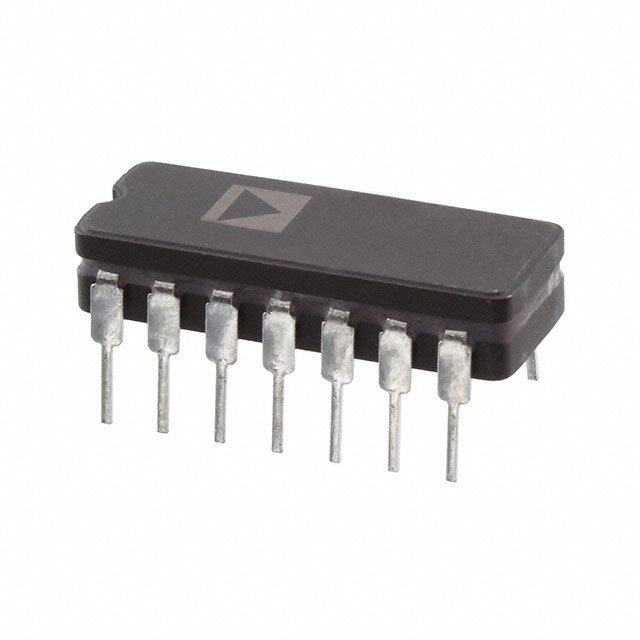
| 产品图片 |
|
| rohs | 符合RoHS无铅 / 符合限制有害物质指令(RoHS)规范要求 |
| 产品系列 | 放大器 IC,运算放大器 - 运放,Texas Instruments LMV792MM/NOPB- |
| 数据手册 | |
| 产品型号 | LMV792MM/NOPB |
| 产品目录页面 | |
| 产品种类 | 运算放大器 - 运放 |
| 供应商器件封装 | 10-VSSOP |
| 共模抑制比—最小值 | 80 dB |
| 关闭 | Shutdown |
| 其它名称 | LMV792MM/NOPBDKR |
| 包装 | Digi-Reel® |
| 压摆率 | 11.5 V/µs |
| 商标 | Texas Instruments |
| 增益带宽生成 | 17 MHz |
| 增益带宽积 | 17MHz |
| 安装类型 | 表面贴装 |
| 安装风格 | SMD/SMT |
| 封装 | Reel |
| 封装/外壳 | 10-TFSOP,10-MSOP(0.118",3.00mm 宽) |
| 封装/箱体 | VSSOP-10 |
| 工作温度 | -40°C ~ 125°C |
| 工作电源电压 | 3 V, 5 V |
| 工厂包装数量 | 1000 |
| 放大器类型 | 通用 |
| 最大工作温度 | + 125 C |
| 最小工作温度 | - 40 C |
| 标准包装 | 1 |
| 电压-电源,单/双 (±) | 1.8 V ~ 5.5 V |
| 电压-输入失调 | 100µV |
| 电流-电源 | 1.3mA |
| 电流-输入偏置 | 0.1pA |
| 电流-输出/通道 | 60mA |
| 电源电流 | 1.3 mA |
| 电路数 | 2 |
| 系列 | LMV792 |
| 设计资源 | http://www.digikey.com/product-highlights/cn/zh/texas-instruments-webench-design-center/3176 |
| 转换速度 | 9.5 V/us |
| 输入偏压电流—最大 | 1 pA |
| 输入补偿电压 | 1.35 mV |
| 输出电流 | 60 mA |
| 输出类型 | 满摆幅 |
| 通道数量 | 2 Channel |


- 商务部:美国ITC正式对集成电路等产品启动337调查
- 曝三星4nm工艺存在良率问题 高通将骁龙8 Gen1或转产台积电
- 太阳诱电将投资9.5亿元在常州建新厂生产MLCC 预计2023年完工
- 英特尔发布欧洲新工厂建设计划 深化IDM 2.0 战略
- 台积电先进制程称霸业界 有大客户加持明年业绩稳了
- 达到5530亿美元!SIA预计今年全球半导体销售额将创下新高
- 英特尔拟将自动驾驶子公司Mobileye上市 估值或超500亿美元
- 三星加码芯片和SET,合并消费电子和移动部门,撤换高东真等 CEO
- 三星电子宣布重大人事变动 还合并消费电子和移动部门
- 海关总署:前11个月进口集成电路产品价值2.52万亿元 增长14.8%


PDF Datasheet 数据手册内容提取
Product Sample & Technical Tools & Support & Folder Buy Documents Software Community LMV791,LMV792 SNOSAG6G–SEPTEMBER2005–REVISEDOCTOBER2015 LMV79x 17-MHz, Low-Noise, CMOS Input, 1.8-V Operational Amplifiers With Shutdown 1 Features 3 Description Typical5-VSupply,UnlessOtherwiseNoted The LMV791 (single) and the LMV792 (dual) low- 1 noise, CMOS input operational amplifiers offer a low • InputReferredVoltageNoise5.8nV/√Hz input voltage noise density of 5.8 nV/√Hz while • InputBiasCurrent100fA consuming only 1.15 mA (LMV791) of quiescent • UnityGainBandwidth17MHz current. The LMV791 and LMV792 are unity gain stableoperationalamplifiersandhavegainbandwidth • SupplyCurrentperChannelEnableMode of 17 MHz. The LMV79x have a supply voltage range – LMV7911.15mA of 1.8 V to 5.5 V and can operate from a single – LMV7921.30mA supply. The LMV79x each feature a rail-to-rail output stage capable of driving a 600-Ω load and sourcing • SupplyCurrentperChannelinShutdownMode asmuchas60mAofcurrent. 0.02µA • Rail-to-RailOutputSwing The LMV79x family provides optimal performance in low-voltage and low-noise systems. A CMOS input – At10-kΩ Load,25mVfromRail stage, with typical input bias currents in the range of – At2-kΩLoad,45mVfromRail a few femtoamperes, and an input common-mode • Ensured2.5-Vand5-VPerformance voltage range which includes ground, make the LMV791 and the LMV792 ideal for low-power sensor • TotalHarmonicDistortion0.01%at1kHz,600Ω applications. The LMV79x family has a built-in enable • TemperatureRange −40°Cto125°C feature which can be used to optimize power dissipationinlowpowerapplications. 2 Applications The LMV791x are manufactured using TI’s advanced • PhotodiodeAmplifiers VIP50 process and are offered in a 6-pin SOT and a • ActiveFiltersandBuffers 10-pinVSSOPpackagerespectively. • Low-NoiseSignalProcessing DeviceInformation(1) • MedicalInstrumentation PARTNUMBER PACKAGE BODYSIZE(NOM) • SensorInterfaceApplications LMV791 SOT(6) 2.90mm×1.60mm LMV792 VSSOP(10) 3.00mm×3.00mm (1) For all available packages, see the orderable addendum at theendofthedatasheet. PhotodiodeTransimpedanceAmplifier Low-NoiseCMOSInput CF 100 + V = 5.5V RF IIN Hz) V+ = 2.5V - /V CCM + + n( E 10 CD -VOUT SION E G A VB CIN = CD + CCM TLO V V OUT = - RF 1 IIN 1 10 100 1k 10k 100k FREQUENCY (Hz) 1 An IMPORTANT NOTICE at the end of this data sheet addresses availability, warranty, changes, use in safety-critical applications, intellectualpropertymattersandotherimportantdisclaimers.PRODUCTIONDATA.
LMV791,LMV792 SNOSAG6G–SEPTEMBER2005–REVISEDOCTOBER2015 www.ti.com Table of Contents 1 Features.................................................................. 1 7.4 DeviceFunctionalModes........................................17 2 Applications........................................................... 1 8 ApplicationandImplementation........................ 19 3 Description............................................................. 1 8.1 ApplicationInformation............................................19 4 RevisionHistory..................................................... 2 8.2 TypicalApplications ...............................................19 5 PinConfigurationandFunctions......................... 3 9 PowerSupplyRecommendations...................... 24 6 Specifications......................................................... 4 10 Layout................................................................... 24 6.1 AbsoluteMaximumRatings......................................4 10.1 LayoutGuidelines.................................................24 6.2 ESDRatings..............................................................4 10.2 LayoutExample....................................................24 6.3 RecommendedOperatingConditions.......................4 11 DeviceandDocumentationSupport................. 25 6.4 ThermalInformation..................................................4 11.1 DeviceSupport ....................................................25 6.5 2.5-VElectricalCharacteristics ................................5 11.2 DocumentationSupport .......................................25 6.6 5-VElectricalCharacteristics ...................................6 11.3 RelatedLinks........................................................25 6.7 TypicalCharacteristics..............................................8 11.4 CommunityResources..........................................25 7 DetailedDescription............................................ 16 11.5 Trademarks...........................................................25 7.1 Overview.................................................................16 11.6 ElectrostaticDischargeCaution............................25 7.2 FunctionalBlockDiagram.......................................16 11.7 Glossary................................................................26 7.3 FeatureDescription.................................................16 12 Mechanical,Packaging,andOrderable Information........................................................... 26 4 Revision History NOTE:Pagenumbersforpreviousrevisionsmaydifferfrompagenumbersinthecurrentversion. ChangesfromRevisionF(March2013)toRevisionG Page • AddedPinConfigurationandFunctionssection,ESDRatingstable,FeatureDescriptionsection,DeviceFunctional Modes,ApplicationandImplementationsection,PowerSupplyRecommendationssection,Layoutsection,Device andDocumentationSupportsection,andMechanical,Packaging,andOrderableInformationsection .............................. 1 • UpdatedtheformatoftheEnableandShutdownPinVoltageRangeinthe2.5-VElectricalCharacteristicstablefor clarity...................................................................................................................................................................................... 5 • UpdatedtheformatoftheEnableandShutdownPinVoltageRangeinthe5-VElectricalCharacteristicstableforclarity.7 ChangesfromRevisionE(March2013)toRevisionF Page • ChangedlayoutofNationalDataSheettoTIformat........................................................................................................... 23 2 SubmitDocumentationFeedback Copyright©2005–2015,TexasInstrumentsIncorporated ProductFolderLinks:LMV791 LMV792
LMV791,LMV792 www.ti.com SNOSAG6G–SEPTEMBER2005–REVISEDOCTOBER2015 5 Pin Configuration and Functions LMV791DDCPackage 6-PinSOT TopView OUTPUT 1 6 V+ 5 EN - 2 V + - 3 4 +IN -IN PinFunctions—LMV791 PIN I/O DESCRIPTION NAME NO. EN 5 I Enable +IN 3 I NoninvertingInput –IN 4 I InvertingInput Out 1 O Output V+ 6 P Positive(highest)SupplyVoltage V– 2 P Negative(lowest)SupplyVoltage LMV792DGSPackage 10-PinVSSOP TopView OUT A 1 10 V+ 2 9 IN A- + OUT B - 3 8 IN A+ + IN B- - V- 4 7 IN B+ 5 6 EN A EN B PinFunctions—LMV792 PIN I/O DESCRIPTION NAME NO. ENA 5 I EnableA ENB 6 I EnableB INA+ 3,7 I InvertingInput INA– 2,8 I NoninvertingInput Out 1 O OutputB OutB 9 O OutputB V+ 10 P Positive(highest)SupplyVoltage V– 4 P Negative(lowest)SupplyVoltage Copyright©2005–2015,TexasInstrumentsIncorporated SubmitDocumentationFeedback 3 ProductFolderLinks:LMV791 LMV792
LMV791,LMV792 SNOSAG6G–SEPTEMBER2005–REVISEDOCTOBER2015 www.ti.com 6 Specifications 6.1 Absolute Maximum Ratings See (1)(2) MIN MAX UNIT V differential ±0.3 V IN Supplyvoltage(V+–V−) 6 V Input/Outputpinvoltage V++0.3 V−−0.3 V Junctiontemperature(3) 150 °C Soldering Infraredorconvection(20sec) 235 °C information Wavesolderingleadtemperature(10sec) 260 °C Storagetemperature,T −65 150 °C stg (1) StressesbeyondthoselistedunderAbsoluteMaximumRatingsmaycausepermanentdamagetothedevice.Thesearestressratings only,whichdonotimplyfunctionaloperationofthedeviceattheseoranyotherconditionsbeyondthoseindicatedunderRecommended OperatingConditions.Exposuretoabsolute-maximum-ratedconditionsforextendedperiodsmayaffectdevicereliability. (2) IfMilitary/Aerospacespecifieddevicesarerequired,pleasecontacttheTexasInstrumentsSalesOffice/Distributorsforavailabilityand specifications. (3) ThemaximumpowerdissipationisafunctionofT ,θ .Themaximumallowablepowerdissipationatanyambienttemperatureis J(MAX) JA P =(T -T )/θ .AllnumbersapplyforpackagessoldereddirectlyontoaPCB. D J(MAX) A JA 6.2 ESD Ratings VALUE UNIT Humanbodymodel(HBM),perANSI/ESDA/JEDECJS-001(1)(2) ±2000 V Electrostatic Charged-devicemodel(CDM),perJEDECspecificationJESD22-C101(3) ±1000 V (ESD) discharge Machinemodel(4) ±200 (1) JEDECdocumentJEP155statesthat500-VHBMallowssafemanufacturingwithastandardESDcontrolprocess. (2) HumanBodyModelis1.5kΩinserieswith100pF. (3) JEDECdocumentJEP157statesthat250-VCDMallowssafemanufacturingwithastandardESDcontrolprocess. (4) MachineModelis0Ωinserieswith200pF 6.3 Recommended Operating Conditions MIN MAX UNIT Temperature(1) −40 125 °C Supplyvoltage −40°C≤TJ≤125°C 2 5.5 V (V+–V−) 0°C≤T ≤125°C 1.8 5.5 V J (1) ThemaximumpowerdissipationisafunctionofT ,θ .Themaximumallowablepowerdissipationatanyambienttemperatureis J(MAX) JA P =(T -T )/θ .AllnumbersapplyforpackagessoldereddirectlyontoaPCB. D J(MAX) A JA 6.4 Thermal Information LMV791 LMV792 THERMALMETRIC(1) DDC(SOT-23) DGS(VSSOP) UNIT 6PINS 10PINS R Junction-to-ambientthermalresistance(2) 191.8 179.1 °C/W θJA R Junction-to-case(top)thermalresistance 68.1 70.5 °C/W θJC(top) R Junction-to-boardthermalresistance 36.9 99.7 °C/W θJB ψ Junction-to-topcharacterizationparameter 2.2 11.6 °C/W JT ψ Junction-to-boardcharacterizationparameter 36.5 98.2 °C/W JB (1) Formoreinformationabouttraditionalandnewthermalmetrics,seetheSemiconductorandICPackageThermalMetricsapplication report,SPRA953. (2) ThemaximumpowerdissipationisafunctionofT ,θ .Themaximumallowablepowerdissipationatanyambienttemperatureis J(MAX) JA P =(T -T )/θ .AllnumbersapplyforpackagessoldereddirectlyontoaPCB. D J(MAX) A JA 4 SubmitDocumentationFeedback Copyright©2005–2015,TexasInstrumentsIncorporated ProductFolderLinks:LMV791 LMV792
LMV791,LMV792 www.ti.com SNOSAG6G–SEPTEMBER2005–REVISEDOCTOBER2015 6.5 2.5-V Electrical Characteristics Unlessotherwisespecified,alllimitsareensuredforT =25°C,V+=2.5V,V−=0V,V =V+/2=V ,V =V+. J CM O EN PARAMETER TESTCONDITIONS MIN(1) TYP(2) MAX(1) UNIT VOS Inputoffsetvoltage T−4J0=°C25≤°CTJ≤125°C 0.1 ±±11..3655 mV LMV791(3) −1 TCVOS Inputoffsetvoltagetemperaturedrift LMV792(3) −1.8 μV/°C TJ=25°C 0.05 1 IB Inputbiascurrent VCM=1V(4)(5) −40°C≤TJ≤85°C 25 pA −40°C≤TJ≤125°C 100 IOS Inputoffsetcurrent VCM=1V(5) 10 fA CMRR Common-moderejectionratio 0V≤VCM≤1.4V T−4J0=°C25≤°CTJ≤125°C 8705 94 dB 2.0V≤V+≤5.5V,VCM=0 TJ=25°C 80 100 PSRR Powersupplyrejectionratio V −40°C≤TJ≤125°C 75 dB 1.8V≤V+≤5.5V,VCM=0V 80 98 CMVR Common-modevoltagerange CMRR≥60dB TJ=25°C −0.3 1.5 V CMRR≥55dB −40°C≤TJ≤125°C −0.3 1.5 LMV791 TJ=25°C 85 98 VOUT=0.15Vto2.2V, −40°C≤TJ≤125°C 80 AVOL Open-loopvoltagegain RLOAD=2kΩtoV+/2 LMV792 T−4J0=°C25≤°CTJ≤125°C 8728 92 dB VOUT=0.15Vto2.2V, TJ=25°C 88 110 RLOAD=10kΩtoV+/2 −40°C≤TJ≤125°C 84 Outputvoltageswinghigh RLOAD=2kΩtoV+/2 T−4J0=°C25≤°CTJ≤125°C 25 7852 VOUT Outputvoltageswinglow RRLLOOAADD==120kΩkΩtotoVV+/+2/2 T−T−44JJ00==°°CC2255≤≤°°CCTTJJ≤≤112255°°CC 2300 67775158 emitVhefrrormail RLOAD=10kΩtoV+/2 T−4J0=°C25≤°CTJ≤125°C 15 6657 SourcingtoV− TJ=25°C 35 47 IOUT Outputcurrent VSiINnk=in2g0t0omVV+(6) −T4J0=°C25≤°CTJ≤125°C 278 15 mA VIN=–200mV(6) −40°C≤TJ≤125°C 5 LMV791 TJ=25°C 0.95 1.3 Enablemode −40°C≤TJ≤125°C 1.65 mA VEN≥2.1V LMV792 TJ=25°C 1.1 1.50 IS Supplycurrentperamplifier perchannel −40°C≤TJ≤125°C 1.85 Shutdownmode,VEN< TJ=25°C 0.02 1 0.4 μA perchannel −40°C≤TJ≤125°C 5 SR Slewrate AV=+1,Rising(10%to90%) 8.5 V/μs AV=+1,Falling(90%to10%) 10.5 GBW Gainbandwidth 14 MHz en Inputreferredvoltagenoisedensity f=1kHz 6.2 nV/√Hz in Inputreferredcurrentnoisedensity f=1kHz 0.01 pA/√Hz ton Turnontime 140 ns toff Turnofftime 1000 ns Enablemode 2.1 2 VEN Enablepinvoltagerange Shutdownmode 0.5 0.4 V (1) Limitsare100%productiontestedat25°C.Limitsovertheoperatingtemperaturerangeareensuredthroughcorrelationsusingthe statisticalqualitycontrol(SQC)method. (2) Typicalvaluesrepresenttheparametricnormatthetimeofcharacterization. (3) OffsetvoltageaveragedriftisdeterminedbydividingthechangeinV bytemperaturechange. OS (4) Positivecurrentcorrespondstocurrentflowingintothedevice. (5) Thisparameterisspecifiedbydesignand/orcharacterizationandisnottestedinproduction. (6) Theshortcircuittestisamomentarytest,theshortcircuitdurationis1.5ms. Copyright©2005–2015,TexasInstrumentsIncorporated SubmitDocumentationFeedback 5 ProductFolderLinks:LMV791 LMV792
LMV791,LMV792 SNOSAG6G–SEPTEMBER2005–REVISEDOCTOBER2015 www.ti.com 2.5-V Electrical Characteristics (continued) Unlessotherwisespecified,alllimitsareensuredforT =25°C,V+=2.5V,V−=0V,V =V+/2=V ,V =V+. J CM O EN PARAMETER TESTCONDITIONS MIN(1) TYP(2) MAX(1) UNIT IEN Enablepininputcurrent ESnhaubtdleowmnomdeodVeENV=EN2=.50VV(4()4) 0.010.35 0.13 μA THD+N Totalharmonicdistortion+noise f=1kHz,AV=1,RLOAD=600Ω 0.01% 6.6 5-V Electrical Characteristics Unlessotherwisespecified,alllimitsareensuredforT =25°C,V+=5V,V−=0V,V =V+/2=V ,V =V+. J CM O EN PARAMETER TESTCONDITIONS MIN(1) TYP(2) MAX(1) UNIT VOS Inputoffsetvoltage T−4J0=°C25≤°CTJ≤125°C 0.1 ±±11..3655 mV LMV791(3) −1 TCVOS Inputoffsetvoltagetemperaturedrift LMV792(3) −1.8 μV/°C TJ=25°C 0.1 1 IB Inputbiascurrent VCM=2V(4)(5) −40°C≤TJ≤85°C 25 pA −40°C≤TJ≤125°C 100 IOS Inputoffsetcurrent VCM=2V(5) 10 fA CMRR Common-moderejectionratio 0V≤VCM≤3.7V T−4J0=°C25≤°CTJ≤125°C 8705 100 dB 2.0V≤V+≤5.5V,VCM= TJ=25°C 80 100 PSRR Powersupplyrejectionratio 0V −40°C≤TJ≤125°C 75 dB 1.8V≤V+≤5.5V,VCM=0V 80 98 CMVR Common-modevoltagerange CMRR≥60dB TJ=25°C −0.3 4 V CMRR≥55dB −40°C≤TJ≤125°C −0.3 4 LMV791 TJ=25°C 85 97 VOUT=0.3Vto4.7V, −40°C≤TJ≤125°C 80 AVOL Open-loopvoltagegain RLOAD=2kΩtoV+/2 LMV792 T−4J0=°C25≤°CTJ≤125°C 8728 89 dB VOUT=0.3Vto4.7V, TJ=25°C 88 110 RLOAD=10kΩtoV+/2 −40°C≤TJ≤125°C 84 Outputvoltageswinghigh RLOAD=2kΩtoV+/2 T−4J0=°C25≤°CTJ≤125°C 35 7852 RLOAD=10kΩtoV+/2 T−4J0=°C25≤°CTJ≤125°C 25 6751 VOUT Outputvoltageswinglow RLOAD=2kΩtoV+/2 LLMMVV779912 T−T4JJ0==°C2255≤°°CCTJ≤125°C 4425 778580 emitVhefrrormail −40°C≤TJ≤125°C 83 RLOAD=10kΩtoV+/2 T−4J0=°C25≤°CTJ≤125°C 20 6657 SourcingtoV− TJ=25°C 45 60 IOUT Outputcurrent VSiINnk=in2g0t0omVV+(6) −T4J0=°C25≤°CTJ≤125°C 3170 21 mA VIN=–200mV(6) −40°C≤TJ≤125°C 6 LMV791 TJ=25°C 1.15 1.4 Enablemode −40°C≤TJ≤125°C 1.75 mA IS Supplycurrentperamplifier VEN≥4.6V LpMerVc7h9a2nnel T−4J0=°C25≤°CTJ≤125°C 1.3 21.0.75 Shutdownmode(VEN≤ TJ=25°C 0.14 1 μA 0.4V) −40°C≤TJ≤125°C 5 (1) Limitsare100%productiontestedat25°C.Limitsovertheoperatingtemperaturerangeareensuredthroughcorrelationsusingthe statisticalqualitycontrol(SQC)method. (2) Typicalvaluesrepresenttheparametricnormatthetimeofcharacterization. (3) OffsetvoltageaveragedriftisdeterminedbydividingthechangeinV bytemperaturechange. OS (4) Positivecurrentcorrespondstocurrentflowingintothedevice. (5) Thisparameterisspecifiedbydesignand/orcharacterizationandisnottestedinproduction. (6) Theshortcircuittestisamomentarytest,theshortcircuitdurationis1.5ms. 6 SubmitDocumentationFeedback Copyright©2005–2015,TexasInstrumentsIncorporated ProductFolderLinks:LMV791 LMV792
LMV791,LMV792 www.ti.com SNOSAG6G–SEPTEMBER2005–REVISEDOCTOBER2015 5-V Electrical Characteristics (continued) Unlessotherwisespecified,alllimitsareensuredforT =25°C,V+=5V,V−=0V,V =V+/2=V ,V =V+. J CM O EN PARAMETER TESTCONDITIONS MIN(1) TYP(2) MAX(1) UNIT SR Slewrate AV=+1,Rising(10%to90%) 6 9.5 V/μs AV=+1,Falling(90%to10%) 7.5 11.5 GBW Gainbandwidth 17 MHz en Inputreferredvoltagenoisedensity f=1kHz 5.8 nV/√Hz in Inputreferredcurrentnoisedensity f=1kHz 0.01 pA/√Hz ton Turnontime 110 ns toff Turnofftime 800 ns Enablemode 4.6 4.5 VEN Enablepinvoltagerange Shutdownmode 0.5 0.4 V IEN Enablepininputcurrent ESnhaubtdleowmnomdeodVeENV=EN5=V0(4)V(4) 0.050.65 01.20 μA THD+N Totalharmonicdistortion+noise f=1kHz,AV=1,RLOAD=600Ω 0.01% Copyright©2005–2015,TexasInstrumentsIncorporated SubmitDocumentationFeedback 7 ProductFolderLinks:LMV791 LMV792
LMV791,LMV792 SNOSAG6G–SEPTEMBER2005–REVISEDOCTOBER2015 www.ti.com 6.7 Typical Characteristics Unlessotherwisespecified,T =25°C,V–=0,V+=SupplyVoltage=5V,V =V+/2,V =V+. A CM EN 2 2 125°C )Am 1.6 125°C )Am 1.6 25°C ( T 25°C ( T NE 1.2 NE 1.2 R R R R U U C C -40°C YL 0.8 -40°C YL 0.8 P P P P U U S 0.4 S 0.4 0 0 1.5 2.5 3.5 4.5 5.5 6.0 1.5 2.5 3.5 4.5 5.5 6 V+ (V) V+ (V) Figure1.SupplyCurrentvsSupplyVoltage(LMV791) Figure2.SupplyCurrentvsSupplyVoltage(LMV792) 1.8 0.5 + V = 1.8V 1.6 0.45 125°C )A 1.4 0.4 P ( T 1.2 -40°C N 0.35 ER 1 )Vm RUC 0.8 ( SO 0.3 25°C Y V 0.25 LP 0.6 PU 25°C 0.2 S 0.4 125°C 0.2 0.15 -40°C 0 0.1 1.5 2.5 3.5 4.5 5.5 6.0 -0.3 0 0.3 0.6 0.9 1.2 V+ (V) VCM (V) Figure3.SupplyCurrentvs Figure4.V vsV OS CM SupplyVoltageinShutdownMode 0.6 0.5 V+ = 2.5V V+ = 5V 0.55 0.45 125°C 0.5 0.4 -40°C 0.45 0.35 )V 0.4 )V 0.3 m m ( SO 0.35 25°C ( SO 0.25 25°C V 0.3 V 0.2 0.25 0.15 -40°C 0.2 0.1 125°C 0.15 0.05 0.1 0 -0.3 0.4 1.1 1.8 -0.3 0.6 1.5 2.4 3.3 4.2 VCM (V) VCM (V) Figure5.V vsV Figure6.V vsV OS CM OS CM 8 SubmitDocumentationFeedback Copyright©2005–2015,TexasInstrumentsIncorporated ProductFolderLinks:LMV791 LMV792
LMV791,LMV792 www.ti.com SNOSAG6G–SEPTEMBER2005–REVISEDOCTOBER2015 Typical Characteristics (continued) Unlessotherwisespecified,T =25°C,V–=0,V+=SupplyVoltage=5V,V =V+/2,V =V+. A CM EN 0.5 13 0.45 12 0.4 0.35 -40°C )sP 11 FALLING )Vm( VSO 00.02..253 25°C /V( ETAR W 109 E 0.15 LS 8 0.1 125°C RISING 7 0.05 0 6 1.5 2.5 3.5 4.5 5.5 6.0 1.8 2.3 2.8 3.3 3.8 4.3 4.8 5.35.5 V+ (V) V+ (V) Figure7.V vsSupplyVoltage Figure8.SlewRatevsSupplyVoltage OS 1.5 2.4 V+ = 2.5V 125°C V+ = 5V 1.3 125°C 1.9 )Am 1.1 25°C )Am 25°C ( TNE 0.9 -40°C ( TNE 1.4 R R RUC 0.7 RUC -40°C Y 0.5 Y 0.9 LP LP -40°C P P U 0.3 U S S 0.4 0.1 125°C -0.1 -0.1 0 0.5 1 1.5 2 2.5 0 1 2 3 4 5 ENABLE PIN VOLTAGE (V) ENABLE PIN VOLTAGE (V) Figure9.SupplyCurrentvsEnablePinVoltage(LMV791) Figure10.SupplyCurrentvsEnablePinVoltage(LMV791) 1.7 2.4 V+ = 2.5V 125°C V+ = 5V 1.5 125°C )A 1.3 25°C )A 1.9 m m ( T 1.1 ( T NER 0.9 NER 1.4 25°C R R UC 0.7 -40°C UC YLP 0.5 YLP 0.9 -40°C -40°C P P 25°C U U S 0.3 S 0.4 125°C 0.1 -0.1 -0.1 0 0.5 1 1.5 2 2.5 0 1 2 3 4 5 ENABLE PIN VOLTAGE (V) ENABLE PIN VOLTAGE (V) Figure11.SupplyCurrentvsEnablePinVoltage(LMV792) Figure12.SupplyCurrentvsEnablePinVoltage(LMV792) Copyright©2005–2015,TexasInstrumentsIncorporated SubmitDocumentationFeedback 9 ProductFolderLinks:LMV791 LMV792
LMV791,LMV792 SNOSAG6G–SEPTEMBER2005–REVISEDOCTOBER2015 www.ti.com Typical Characteristics (continued) Unlessotherwisespecified,T =25°C,V–=0,V+=SupplyVoltage=5V,V =V+/2,V =V+. A CM EN 1.5 50 + + V = 5V V = 5V 1 40 -40°C 30 0.5 20 0 125°C )Ap -0.5 )Ap 10 ( S 25°C ( S 0 IAIB -1 IAIB -10 85°C -1.5 -20 -2 -30 -2.5 -40 -3 -50 0 1 2 3 4 0 1 2 3 4 VCM (V) VCM (V) Figure13.InputBiasCurrentvsV Figure14.InputBiasCurrentvsV CM CM 80 35 70 125°C 30 125°C 60 25 )Am( ECRUOS 345000 25°C -40°C )Am( IKNIS 1250 25°C I -40°C 10 20 10 5 0 0 1 2 3 4 5 6 1 2 3 4 5 6 V+ (V) V+ (V) Figure15.SourcingCurrentvsSupplyVoltage Figure16.SinkingCurrentvsSupplyVoltage 70 30 125°C 60 125°C 25 50 20 )A m( IECRUOS 3400 25°C -40°C )Am( IKNIS 1105 25°C 20 -40°C 5 10 0 0 0 1 2 3 4 5 0 1 2 3 4 5 VOUT (V) VOUT (V) Figure17.SourcingCurrentvsOutputVoltage Figure18.SinkingCurrentvsOutputVoltage 10 SubmitDocumentationFeedback Copyright©2005–2015,TexasInstrumentsIncorporated ProductFolderLinks:LMV791 LMV792
LMV791,LMV792 www.ti.com SNOSAG6G–SEPTEMBER2005–REVISEDOCTOBER2015 Typical Characteristics (continued) Unlessotherwisespecified,T =25°C,V–=0,V+=SupplyVoltage=5V,V =V+/2,V =V+. A CM EN 40 25 RLOAD = 10 k: -40°C 35 25°C 20 )V 30 )V m m ( LIAR 25 125°C 25°C ( LIAR 15 M 20 M 125°C O O RF 15 -40°C RF 10 TU TU VO 10 VO 5 5 RLOAD = 10 k: 0 0 1.8 2.5 3.2 3.9 4.6 5.3 6 1.8 2.5 3.2 3.9 4.6 5.3 6 + + V (V) V (V) Figure19.PositiveOutputSwingvsSupplyVoltage Figure20.NegativeOutputSwingvsSupplyVoltage 50 50 -40°C 45 45 125°C 25°C )Vm 40 25°C )V 40 ( LIAR 3305 m( LIA 3350 125°C M R O 25 M 25 R O F VTUO 1250 -40°C RF TUO 1250 V 10 10 5 RLOAD = 2 k: 5 RLOAD = 2 k: 0 0 1.8 2.5 3.2 3.9 4.6 5.3 6 1.8 2.5 3.2 3.9 4.6 5.3 6 V+ (V) V+ (V) Figure21.PositiveOutputSwingvsSupplyVoltage Figure22.NegativeOutputSwingvsSupplyVoltage 100 120 90 RLOAD = 600: RLOAD = 600: 25°C 125°C 100 80 )V 125°C )V m 70 m ( LIA 60 25°C ( LIA 80 -40°C R R M 50 M 60 O O R 40 R F F T -40°C T 40 U 30 U O O V V 20 20 10 0 0 1.8 2.5 3.2 3.9 4.6 5.3 6 1.8 2.5 3.2 3.9 4.6 5.3 6 V+ (V) V+ (V) Figure23.PositiveOutputSwingvsSupplyVoltage Figure24.NegativeOutputSwingvsSupplyVoltage Copyright©2005–2015,TexasInstrumentsIncorporated SubmitDocumentationFeedback 11 ProductFolderLinks:LMV791 LMV792
LMV791,LMV792 SNOSAG6G–SEPTEMBER2005–REVISEDOCTOBER2015 www.ti.com Typical Characteristics (continued) Unlessotherwisespecified,T =25°C,V–=0,V+=SupplyVoltage=5V,V =V+/2,V =V+. A CM EN 100 + VS = ±2.5V V = 5.5V VCM = 0.0V Hz) V+ = 2.5V /V V n( ES 10 ID/V ION E n 004 G A T L O V 1 1 10 100 1k 10k 100k FREQUENCY (Hz) 1S/DIV Figure25.InputReferredVoltageNoisevsFrequency Figure26.TimeDomainVoltageNoise 70 0 + V = 1.2V % TO 60 US% -20 V- = -0.6V OH AV = +2 S 50 RE OS% -40 DN 40 )Bd U D ( N -60 NA TO 30 +DHT -80 RLOAD = 600: O 20 H S R E 10 -100 V O RLOAD = 100 k: 0 -120 0 20 40 60 80 100 120 0.02 0.2 2 CLOAD (pF) OUTPUT AMPLITUDE (V) Figure27.OvershootandUndershootvsCLOAD Figure28.THD+NvsPeak-to-PeakOutputVoltage(VOUT) 0 0.006 + V = 2.75V - -20 V = -2.75V 0.005 RL = 600: AV = +2 -40 0.004 )B )% d( N+DH --8600 RLOAD = 600: ( N+DH 0.003 RL = 100 k: T T 0.002 V+ = 1.2V -100 - V = 0.6V -120 0.001 VO = 0.9 VPP RLOAD = 100 k: AV = +2 -140 0 0.02 0.2 2 4 10 100 1k 10k 100k OUTPUT AMPLITUDE (V) FREQUENCY (Hz) Figure29.THD+NvsPeak-to-PeakOutputVoltage(V ) Figure30.THD+NvsFrequency OUT 12 SubmitDocumentationFeedback Copyright©2005–2015,TexasInstrumentsIncorporated ProductFolderLinks:LMV791 LMV792
LMV791,LMV792 www.ti.com SNOSAG6G–SEPTEMBER2005–REVISEDOCTOBER2015 Typical Characteristics (continued) Unlessotherwisespecified,T =25°C,V–=0,V+=SupplyVoltage=5V,V =V+/2,V =V+. A CM EN 0.006 120 120 PHASE 100 100 0.005 RL = 600: CL = 20 pF 80 80 0.004 60 CL = 50 pF 60 )%( N+D 0.003 VV+- == 22..55VV )Bd( NIA 2400 GAIN CL = 100 pF 2400 (°) ESAH H G P T 0.002 VO = 4 VPP 0 0 AV = +2 -20 CL = 20 pF -20 CL = 50 pF 0.001 -40 CL = 100 pF -40 RL = 100 k: -60 -60 0 10 100 1k 10k 100k 1k 10k 100k 1M 10M 100M FREQUENCY (Hz) FREQUENCY (Hz) Figure31.THD+NvsFrequency Figure32.Open-LoopGainandPhaseWithCapacitiveLoad 120 120 100 PHASE 100 100 80 80 :) 10 ( E 60 60 C N )Bd( NIAG 2400 GAIN 2400 °) E(SAHP ADEPMI T 1 U 0 0 P T U 0.1 -20 -20 O -40 -40 RLOAD = 600:(cid:15)(cid:3)10(cid:3)k:(cid:15) 10 M: 0.01 -60 -60 10 100 1k 10k 100k 1M 10M 100M 10k 100k 1M 10M 100M FREQUENCY (Hz) FREQUENCY (Hz) Figure33.Open-LoopGainandPhaseWithResistiveLoad Figure34.Closed-LoopOutputImpedancevsFrequency 160 )B d( N 140 O IT 120 A R N 100 V OITC 80 V/DI E m JER 60 10 K L A 40 T INPUT = 20 mVPP S SO 20 f = 1 MHz R + C V = 2.5V 0 1k 10k 100k 1M 10M 100M 200 ns/DIV FREQUENCY (Hz) A =+1 V Figure35.CrosstalkRejection Figure36.SmallSignalTransientResponse Copyright©2005–2015,TexasInstrumentsIncorporated SubmitDocumentationFeedback 13 ProductFolderLinks:LMV791 LMV792
LMV791,LMV792 SNOSAG6G–SEPTEMBER2005–REVISEDOCTOBER2015 www.ti.com Typical Characteristics (continued) Unlessotherwisespecified,T =25°C,V–=0,V+=SupplyVoltage=5V,V =V+/2,V =V+. A CM EN V V DI DI V/ V/ m m 00 0 2 1 INPUT = 1 VPP INPUT = 20 mVPP f = 200 kHz f = 1 MHz V+ = 2.5V V+ = 5V 800 ns/DIV 200 ns/DIV A =+1 A =+1 V V Figure37.LargeSignalTransientResponse Figure38.SmallSignalTransientResponse 50 RLOAD = 600: 40 RLOAD = 10 k: mV/DIV )°( NIGRAM 2300 00 ES RLOAD = 10 M: 2 AH 10 P INPUT = 1 VPP 0 f =+ 200 kHz V+ = 2.5V V = 5V -10 10 100 1000 800 ns/DIV A =+1 CLOAD (pF) V Figure39.LargeSignalTransientResponse Figure40.PhaseMarginvsCapacitiveLoad(Stability) 50 0 RLOAD = 600: 40 -20 RLOAD = 10 k: )B )°( NIG 30 d( RR -40 R S AM 20 P E ES RLOAD = 10 M: VIT -60 A 10 IS H O P P 1.8V -80 0 + V = 5V 5.5V -10 -100 10 100 1000 10 100 1k 10k 100k 1M 10M CLOAD (pF) FREQUENCY (Hz) Figure41.PhaseMarginvsCapacitiveLoad(Stability) Figure42.PositivePSRRvsFrequency 14 SubmitDocumentationFeedback Copyright©2005–2015,TexasInstrumentsIncorporated ProductFolderLinks:LMV791 LMV792
LMV791,LMV792 www.ti.com SNOSAG6G–SEPTEMBER2005–REVISEDOCTOBER2015 Typical Characteristics (continued) Unlessotherwisespecified,T =25°C,V–=0,V+=SupplyVoltage=5V,V =V+/2,V =V+. A CM EN -20 120 100 -40 + )B V = 2.5V d ( R 80 RS -60 )B + P E V+ = 1.8V d( R 60 V = 5V VIT -80 RM AG C 40 E N -100 + 20 V = 5.5V -120 0 10 100 1k 10k 100k 1M 10M 10 100 1k 10k 100k 1M FREQUENCY (Hz) FREQUENCY (Hz) Figure43.NegativePSRRvsFrequency Figure44.CMRRvsFrequency 25 + V = 5V 20 )F 15 p ( M C C 10 5 0 0 1 2 3 4 VCM (V) Figure45.InputCommon-ModeCapacitancevsV CM Copyright©2005–2015,TexasInstrumentsIncorporated SubmitDocumentationFeedback 15 ProductFolderLinks:LMV791 LMV792
LMV791,LMV792 SNOSAG6G–SEPTEMBER2005–REVISEDOCTOBER2015 www.ti.com 7 Detailed Description 7.1 Overview The LMV79x family provides optimal performance in low-voltage and low-noise systems. A low-noise CMOS input stage, with typical input bias currents in the range of a few femtoamperes, and an input common-mode voltagerangewhichincludesgroundmaketheLMV791andtheLMV792idealforlow-powersensorapplications 7.2 Functional Block Diagram 7.3 Feature Description 7.3.1 WideBandwidthatLowSupplyCurrent The LMV791 and LMV792 are high performance operational amplifiers that provide a unity gain bandwidth of 17 MHz while drawing a low supply current of 1.15 mA. This makes them ideal for providing wideband amplification in portable applications. The shutdown feature can also be used to design more power efficient systems that offerwidebandwidthandhighperformancewhileconsuminglessaveragepower. 7.3.2 LowInputReferredNoiseandLowInputBiasCurrent The LMV79x have a very low input referred voltage noise density (5.8 nV/√Hz at 1 kHz). A CMOS input stage ensures a small input bias current (100 fA) and low input referred current noise (0.01 pA/√Hz). This is very helpful in maintaining signal fidelity, and makes the LMV791 and LMV792 ideal for audio and sensor-based applications. 7.3.3 LowSupplyVoltage The LMV791 and the LMV792 have performance ensured at 2.5-V and 5-V supply. The LMV791 family is ensured to be operational at all supply voltages between 2 V and 5.5 V, for ambient temperatures ranging from −40°C to 125°C, thus using the entire battery lifetime. The LMV791 and LMV792 are also ensured to be operational at 1.8-V supply voltage, for temperatures between 0°C and 125°C. This makes the LMV791 family idealforusageinlow-voltagecommercialapplications. 7.3.4 Rail-to-RailOutputandGroundSensing Rail-to-rail output swing provides maximum possible dynamic range at the output. This is particularly important whenoperatingatlowsupplyvoltages.Aninnovativepositivefeedbackschemeisusedtoboostthecurrentdrive capability of the output stage. This allows the LMV791 and the LMV792 to source more than 40 mA of current at 1.8-V supply. This also limits the performance of the LMV791 family as comparators, and hence the usage of the LMV791 and the LMV792 in an open-loop configuration is not recommended. The input common-mode range includesthenegativesupplyrailwhichallowsdirectsensingatgroundinsinglesupplyoperation. 7.3.5 ShutdownFeature The LMV791 family is ideal for battery-powered systems. With a low supply current of 1.15 mA and a shutdown current of 140 nA typically, the LMV791 and LMV792 allow the designer to maximize battery life. The enable pin of the LMV791 and the LMV792 allows the operational amplifier to be turned off and reduce its supply current to less than 1 μA. To power on the operational amplifier the enable pin should be higher than V+ – 0.5 V, where V+ is the positive supply. To disable the operational amplifier, the enable pin voltage should be less than V− + 0.5 V, whereV−isthenegativesupply. 16 SubmitDocumentationFeedback Copyright©2005–2015,TexasInstrumentsIncorporated ProductFolderLinks:LMV791 LMV792
LMV791,LMV792 www.ti.com SNOSAG6G–SEPTEMBER2005–REVISEDOCTOBER2015 Feature Description (continued) 7.3.6 SmallSize The small footprint of the LMV791 and the LMV792 package saves space on printed-circuit-boards, and enables the design of smaller electronic products, such as mobile phones, tablets, or other portable systems. Long traces between the signal source and the operational amplifier make the signal path susceptible to noise. By using a physically smaller LMV791 and LMV792 package, the operational amplifier can be placed closer to the signal source,reducingnoisepick-upandincreasingsignalintegrity. 7.4 Device Functional Modes 7.4.1 CapacitiveLoadTolerance The LMV791 and LMV792 can directly drive up to 120 pF in unity gain without oscillation. The unity gain follower is the most sensitive configuration to capacitive loading. Direct capacitive loading reduces the phase margin of amplifiers. The combination of the output impedance of the amplifier and the capacitive load induces phase lag. Thisresultsineitheranunderdampedpulseresponseoroscillation.Todriveaheaviercapacitiveload,thecircuit inFigure46canbeused. In Figure 46, the isolation resistor R and the load capacitor C form a pole to increase stability by adding more ISO L phase margin to the overall system. The desired performance depends on the value of R . The bigger the R ISO ISO resistorvalue,themorestableV willbe.IncreasedR would,however,resultinareducedoutputswingand OUT ISO shortcircuitcurrent. Figure46. IsolationofC toImproveStability L 7.4.2 InputCapacitanceandFeedbackCircuitElements The LMV791 family has a very low input bias current (100 fA) and a low 1/f noise corner frequency (400 Hz), which makes it ideal for sensor applications. However, to obtain this performance a large CMOS input stage is used, which adds to the input capacitance of the operational amplifier, C . Though this does not affect the DC IN and low frequency performance, at higher frequencies the input capacitance interacts with the input and the feedback impedances to create a pole, which results in lower phase margin and gain peaking. This can be controlled by being selective in the use of feedback resistors, as well as by using a feedback capacitance, C . F For example, in the inverting amplifier shown in Figure 47, if C and C are ignored and the open-loop gain of IN F the operational amplifier is considered infinite then the gain of the circuit is −R /R . An operational amplifier, 2 1 however, usually has a dominant pole, which causes its gain to drop with frequency. Hence, this gain is only validforDCandlowfrequency.Tounderstandtheeffectoftheinputcapacitancecoupledwiththenon-idealgain oftheoperationalamplifier,thecircuitneedstobeanalyzedinthefrequencydomainusingaLaplacetransform. CF R2 R1 - VIN+ CIN + + - VOUT - VOUT R2 AV = - VIN = - R1 Figure47. InvertingAmplifier Copyright©2005–2015,TexasInstrumentsIncorporated SubmitDocumentationFeedback 17 ProductFolderLinks:LMV791 LMV792
LMV791,LMV792 SNOSAG6G–SEPTEMBER2005–REVISEDOCTOBER2015 www.ti.com Device Functional Modes (continued) For simplicity, the operational amplifier is modeled as an ideal integrator with a unity gain frequency of A . 0 Hence, its transfer function (or gain) in the frequency domain is A /s. Solving the circuit equations in the 0 frequencydomain,ignoringC forthemoment,resultsinanexpressionforthegainshowninEquation1. F VOUT -R2/R1 (s) = VIN s s2 1 + + § A0 R1 ' § A0 ' ¤ ¤ ¤ ¤ 'R1 + R2§ 'CIN R2§ (1) It can be inferred from the denominator of the transfer function that it has two poles, whose expressions can be obtainedbysolvingfortherootsofthedenominatorandareshowninEquation2. 2 P1,2 =2-C1IN R11 + R12 r ¤'§R11 + R12¤'§ - 4 AR0C2IN (2) Equation 2 shows that as the values of R and R are increased, the magnitude of the poles, and hence the 1 2 bandwidth of the amplifier, is reduced. This theory is verified by using different values of R and R in the circuit 1 2 shown in Figure 46 and by comparing their frequency responses. In Figure 48 the frequency responses for three different values of R and R are shown. When both R and R are 1 kΩ, the response is flattest and widest; 1 2 1 2 whereas, it narrows and peaks significantly when both their values are changed to 10 kΩ or 30 kΩ. So it is advisable to use lower values of R and R to obtain a wider and flatter response. Lower resistances also help in 1 2 high-sensitivitycircuitsbecausetheyaddlessnoise. A way of reducing the gain peaking is by adding a feedback capacitance C in parallel with R . This introduces F 2 another pole in the system and prevents the formation of pairs of complex conjugate poles which cause the gain to peak. Figure 49 shows the effect of C on the frequency response of the circuit. Adding a capacitance of 2 pF F removes the peak, while a capacitance of 5 pF creates a much lower pole and reduces the bandwidth excessively. 15 20 AV = -1 R1, R2 = 30 k: CF = 0 pF 10 10 AV = -1 5 0 )Bd( N -50 )Bd( N -10 CF = 5 pF IAG -10 R1, R2 = 30 k: IAG CF = 2 pF R1, R2 = 10 k: -20 -15 R1, R2 = 1 k: -30 -20 -25 -40 10k 100k 1M 10M 100M 10k 100k 1M 10M FREQUENCY (Hz) FREQUENCY (Hz) Figure48.GainPeakingCausedbyLargeR ,R Figure49.GainPeakingEliminatedbyC 1 2 F 18 SubmitDocumentationFeedback Copyright©2005–2015,TexasInstrumentsIncorporated ProductFolderLinks:LMV791 LMV792
LMV791,LMV792 www.ti.com SNOSAG6G–SEPTEMBER2005–REVISEDOCTOBER2015 8 Application and Implementation NOTE Information in the following applications sections is not part of the TI component specification, and TI does not warrant its accuracy or completeness. TI’s customers are responsible for determining suitability of components for their purposes. Customers should validateandtesttheirdesignimplementationtoconfirmsystemfunctionality. 8.1 Application Information The LMV791 and LMV792 family of amplifiers is specified for operation from 1.8 V to 5.5 V. Parameters that can exhibit significant variance with regard to operating voltage or temperature are presented in the Typical Characteristicssection. 8.2 Typical Applications TheseapplicationexampleshighlightafewofthecircuitswheretheLMV791andLMV792maybeused. 8.2.1 TransimpedanceAmplifier CMOSinputoperationalamplifiersareoftenusedintransimpedanceapplicationsastheyhaveanextremelyhigh input impedance. A transimpedance amplifier converts a small input current into a voltage. This current is usually generated by a photodiode. The transimpedance gain, measured as the ratio of the output voltage to the input current, is expected to be large and wide-band. Because the circuit deals with currents in the range of a few nA, low-noise performance is essential. The LMV79x are CMOS input operational amplifiers providing wide bandwidthandlownoiseperformance,andarehenceidealfortransimpedanceapplications. CF RF IIN - CCM + + VOUT CD - VB CIN = CD + CCM V OUT = - RF IIN Figure50. PhotodiodeTransimpedanceAmplifier 8.2.1.1 DesignRequirements Usually, a transimpedance amplifier is designed on the basis of the current source driving the input. A photodiode is a very common capacitive current source, which requires transimpedance gain for transforming its miniscule current into easily-detectable voltages. The photodiode and gain of the amplifier are selected with respect to the speed and accuracy required of the circuit. A faster circuit would require a photodiode with lesser capacitance and a faster amplifier. A more sensitive circuit would require a sensitive photodiode and a high gain. A typical transimpedance amplifier is shown in Figure 50. The output voltage of the amplifier is given by the equation V = −I R . Because the output swing of the amplifier is limited, R should be selected such that all OUT IN F F possiblevaluesofI canbedetected. IN Copyright©2005–2015,TexasInstrumentsIncorporated SubmitDocumentationFeedback 19 ProductFolderLinks:LMV791 LMV792
LMV791,LMV792 SNOSAG6G–SEPTEMBER2005–REVISEDOCTOBER2015 www.ti.com Typical Applications (continued) 8.2.1.2 DetailedDesignProcedure The LMV79x have a large gain-bandwidth product (17 MHz), which enables high gains at wide bandwidths. A rail-to-rail output swing at 5.5-V supply allows detection and amplification of a wide range of input currents. A CMOS input stage with negligible input current noise and low input voltage noise allows the LMV79x to provide high-fidelity amplification for wide bandwidths. These properties make the LMV79x ideal for systems requiring wide-bandtransimpedanceamplification. As mentioned earlier, the following parameters are used to design a transimpedance amplifier: the amplifier gain- bandwidth product, A ; the amplifier input capacitance, C ; the photodiode capacitance, C ; the 0 CM D transimpedance gain required, R ; and the amplifier output swing. Once a feasible R is selected using the F F amplifier output swing, these numbers can be used to design an amplifier with the desired transimpedance gain andamaximallyflatfrequencyresponse. An essential component for obtaining a maximally flat response is the feedback capacitor, C . The capacitance F seen at the input of the amplifier, C , combined with the feedback capacitor, R , generate a phase lag which IN F causes gain-peaking and can destabilize the circuit. C is usually just the sum of C and C . The feedback IN D CM capacitor C creates a pole, f in the noise gain of the circuit, which neutralizes the zero in the noise gain, f , F P Z created by the combination of R and C . If properly positioned, the noise gain pole created by C can ensure F IN F that the slope of the gain remains at 20 dB/decade till the unity gain frequency of the amplifier is reached, thus ensuring stability. As shown in Figure 51, f is positioned such that it coincides with the point where the noise P gain intersects the open-loop gain of the operational amplifier. In this case, f is also the overall 3-dB frequency P of the transimpedance amplifier. The value of C needed to make it so is given by Equation 3. A larger value of F C causesexcessivereductionofbandwidth,whileasmallervaluefailstopreventgainpeakingandinstability. F 1 + 1 + 4SR C A F IN 0 C = F 2SR A F 0 (3) OP AMP NOISE GAIN WITH NO CF OPEN LOOP GAIN N 1 GAI fZ = 2SRFCIN NOISE GAIN WITH CF fP = A0 2SRF(CIN+CF) fZ fP A0 FREQUENCY Figure51. C SelectionforStability F Calculating C from Equation 3 can sometimes return unreasonably small values (<1 pF), especially for high- F speed applications. In these cases, its often more practical to use the circuit shown in Figure 52 in order to allow morereasonablevalues.Inthiscircuit,thecapacitanceC ′is(1+R /R )timetheeffectivefeedbackcapacitance, F B A C .Alargercapacitorcannowbeusedinthiscircuittoobtainasmallereffectivecapacitance. F For example, if a C of 0.5 pF is needed, while only a 5-pF capacitor is available, R and R can be selected F B A such that R /R = 9. This would convert a C ′of 5 pF into a C of 0.5 pF. This relationship holds as long as R < B A F F A R . F 20 SubmitDocumentationFeedback Copyright©2005–2015,TexasInstrumentsIncorporated ProductFolderLinks:LMV791 LMV792
LMV791,LMV792 www.ti.com SNOSAG6G–SEPTEMBER2005–REVISEDOCTOBER2015 Typical Applications (continued) RA RB CFc RF - + IF RA < < RF CFc = ¤'§1 +RRBA¤'§CF Figure52. ObtainingSmallC fromlargeC ′ F F 8.2.2 ApplicationCurves The LMV791 was used to design a number of amplifiers with varying transimpedance gains and source capacitances. The gains, bandwidths and feedback capacitances of the circuits created are summarized in Table 1. The frequency responses are presented in Figure 53 and Figure 54. The feedback capacitances are slightly different from the formula in Equation 3, because the parasitic capacitance of the board and the feedback resistorR hadtobeaccountedfor. F Table1.FrequencyResponseResults Transimpedance,A C C 3-dBFrequency TI IN F 470000 50pF 1.5pF 350kHz 470000 100pF 2.0pF 250kHz 470000 200pF 3.0pF 150kHz 47000 50pF 4.5pF 1.5MHz 47000 100pF 6.0pF 1MHz 47000 200pF 9.0pF 700kHz 130 100 CIN = 50 pF, CF = 4.5 pF 120 CIN = 50 pF, CF = 1.5 pF 95 90 110 85 )B 100 )B 80 CIN = 100 pF, CF = 6 pF d( N 90 d( N 75 IAG 80 CIN = 100 pF, CF = 2 pF IAG 70 CIN = 200 pF, CF = 9 pF CIN = 200 pF, CF = 3 pF 65 70 60 60 55 50 50 10k 100k 1M 10M 10k 100k 1M 10M FREQUENCY (Hz) FREQUENCY (Hz) Figure53.FrequencyResponseforATI=470000 Figure54.FrequencyResponseforATI=47000 Copyright©2005–2015,TexasInstrumentsIncorporated SubmitDocumentationFeedback 21 ProductFolderLinks:LMV791 LMV792
LMV791,LMV792 SNOSAG6G–SEPTEMBER2005–REVISEDOCTOBER2015 www.ti.com 8.2.3 High-Gain,WidebandTransimpedanceAmplifierUsingtheLMV792 The LMV792, dual, low-noise, wide-bandwidth, CMOS input operational amplifier IC can be used for compact, robust and integrated solutions for sensing and amplifying wide-band signals obtained from sensitive photodiodes. One of the two operational amplifiers available can be used to obtain transimpedance gain while the other can be used for amplifying the output voltage to further enhance the transimpedance gain. The wide bandwidth of the operational amplifiers (17 MHz) ensures that they are capable of providing high gain for a wide range of frequencies. The low input referred noise (5.8 nV/√Hz) allows the amplifier to deliver an output with a high SNR (signal to noise ratio). The small VSSOP-10 footprint saves space on printed-circuit-boards and allows easeofdesigninportableproducts. ThecircuitshowninFigure55,hasthefirstoperationalamplifieractingasatransimpedanceamplifierwithagain of 47000, while the second stage provides a voltage gain of 10. This provides a total transimpedance gain of 470000 with a −3-dB bandwidth of about 1.5 MHz, for a total input capacitance of 50 pF. The frequency responseforthecircuitisshowninFigure56 4.5 pF 47 k: 10 k: IIN - 1 k: CIN = 50 pF 792A - + 0.1 PF 792B + + VOUT - V A = OUT = 470,000 TI I IN Figure55. 1.5-MHzTransimpedanceAmplifier,WithA =470000 TI 120 110 100 )B d ( N 90 IA G 80 70 CIN = 50 pF CF = 4.5 pF 60 10k 100k 1M 10M FREQUENCY (Hz) Figure56. 1.5-MHzTransimpedanceAmplifierFrequencyResponse 8.2.4 AudioPreamplifierWithBandpassFiltering With low input referred voltage noise, low supply voltage and low supply current, and a low harmonic distortion, the LMV791 family is ideal for audio applications. Its wide unity gain bandwidth allows it to provide large gain for a wide range of frequencies and it can be used to design a preamplifier to drive a load of as low as 600 Ω with less than 0.01% distortion. Two amplifier circuits are shown in Figure 57 and Figure 58. Figure 57 is an inverting amplifier, with a 10-kΩ feedback resistor, R , and a 1-kΩ input resistor, R , and hence provides a gain of −10. 2 1 Figure 58 is a noninverting amplifier, using the same values of R and R , and provides a gain of 11. In either of 1 2 these circuits, the coupling capacitor C decides the lower frequency at which the circuit starts providing gain, C1 while the feedback capacitor C decides the frequency at which the gain starts dropping off. Figure 59 shows the F frequencyresponseoftheinvertingamplifierwithdifferentvaluesofC . F 22 SubmitDocumentationFeedback Copyright©2005–2015,TexasInstrumentsIncorporated ProductFolderLinks:LMV791 LMV792
LMV791,LMV792 www.ti.com SNOSAG6G–SEPTEMBER2005–REVISEDOCTOBER2015 CF V+ R1 R2 CC1 1 k: 10 k: CC2 RB1 + + VIN- V+ RB1 +- CC2 +-VOUT VIN+- RB2 -10R k2: +-VOUT RB2 R1 CF 1 k: AV = - RR21 = -10 CC1 AV = 1 +RR2 = 11 1 Figure57.InvertingAudioPreamplifier Figure58.NoninvertingAudioPreamplifier 25 CF = 10 pF 20 15 CF = 1 nF 10 )B CF = 100 pF d 5 ( N IA 0 G -5 -10 -15 -20 1 10 100 1k 10k 100k 1M FREQUENCY (Hz) Figure59.FrequencyResponseoftheInvertingAudioPreamplifier 8.2.5 SensorInterfaces The low input bias current and low input referred noise of the LMV791 and LMV792 make them ideal for sensor interfaces. These circuits are required to sense voltages of the order of a few μV, and currents amounting to less than a nA, and hence the operational amplifier needs to have low voltage noise and low input bias current. Typical applications include infrared (IR) thermometry, thermocouple amplifiers and pH electrode buffers. Figure60isanexampleofatypicalcircuitusedformeasuringIRradiationintensity,oftenusedforestimatingthe temperature of an object from a distance. The IR sensor generates a voltage proportional to I, which is the intensity of the IR radiation falling on it. As shown in Figure 60, K is the constant of proportionality relating the voltage across the IR sensor (V ) to the radiation intensity, I. The resistances R and R are selected to provide IN A B ahighgaintoamplifythisvoltage,whileC isaddedtofilteroutthehigh-frequencynoise. F IR SENSOR + + - + V-IN = KI RB VOUT - IR RADIATION INTENSITY, I RA CF VOUT RA I = K(RA + RB) Figure60. IRRadiationSensor Copyright©2005–2015,TexasInstrumentsIncorporated SubmitDocumentationFeedback 23 ProductFolderLinks:LMV791 LMV792
LMV791,LMV792 SNOSAG6G–SEPTEMBER2005–REVISEDOCTOBER2015 www.ti.com 9 Power Supply Recommendations For proper operation, the power supplies must be properly decoupled. For decoupling the supply lines, TI recommendsthat10-nFcapacitorsbeplacedascloseaspossibletotheoperationalamplifierpowersupplypins. For single-supply, place a capacitor between V+ and V– supply leads. For dual supplies, place one capacitor betweenV+andground,andonecapacitorbetweenV–andground. 10 Layout 10.1 Layout Guidelines Connect low-ESR, 0.1-μF ceramic bypass capacitors between each supply pin and ground, placed as close to thedeviceaspossible.AsinglebypasscapacitorfromV+togroundisapplicableforsingle-supplyapplications. Noise can propagate into analog circuitry through the power pins of the circuit as a whole and operational amplifier itself. Bypass capacitors are used to reduce the coupled noise by providing low-impedance power sourceslocaltotheanalogcircuitry. Separate grounding for analog and digital portions of circuitry is one of the simplest and most-effective methods of noise suppression. One or more layers on multilayer PCBs are usually devoted to ground planes. A ground plane helps distribute heat and reduces EMI noise pickup. Make sure to physically separate digital and analog grounds,payingattentiontotheflowofthegroundcurrent. ThegroundpinshouldbeconnectedtothePCBgroundplaneatthepinofthedevice. Thefeedbackcomponentsshouldbeplacedasclosetothedeviceaspossibleminimizingstrays. 10.2 Layout Example Figure61. TypicalSOTLayout 24 SubmitDocumentationFeedback Copyright©2005–2015,TexasInstrumentsIncorporated ProductFolderLinks:LMV791 LMV792
LMV791,LMV792 www.ti.com SNOSAG6G–SEPTEMBER2005–REVISEDOCTOBER2015 11 Device and Documentation Support 11.1 Device Support 11.1.1 DevelopmentSupport Fordevelopmentalsupport,seethefollowing: • LMV791PSPICEModel,SNOM056 • LMV792PSPICEModel,SNOM057 • TINA-TISPICE-BasedAnalogSimulationProgram,http://www.ti.com/tool/tina-ti • DIPAdapterEvaluationModule,http://www.ti.com/tool/dip-adapter-evm • TIUniversalOperationalAmplifierEvaluationModule,http://www.ti.com/tool/opampevm • TIFilterproSoftware,http://www.ti.com/tool/filterpro 11.2 Documentation Support 11.2.1 RelatedDocumentation Forrelateddocumentation,seethefollowing: • AN-31OpAmpCircuitCollection,SNLA140 • FeedbackPlotsDefineOpAmpACPerformance, SBOA015(AB-028) • CircuitBoardLayoutTechniques,SLOA089 • OpAmpsforEveryone,SLOD006 • CapacitiveLoadDriveSolutionusinganIsolationResistor,TIPD128 • HandbookofOperationalAmplifierApplications,SBOA092 11.3 Related Links The table below lists quick access links. Categories include technical documents, support and community resources,toolsandsoftware,andquickaccesstosampleorbuy. Table2.RelatedLinks TECHNICAL TOOLS& SUPPORT& PARTS PRODUCTFOLDER SAMPLE&BUY DOCUMENTS SOFTWARE COMMUNITY LMV791 Clickhere Clickhere Clickhere Clickhere Clickhere LMV792 Clickhere Clickhere Clickhere Clickhere Clickhere 11.4 Community Resources The following links connect to TI community resources. Linked contents are provided "AS IS" by the respective contributors. They do not constitute TI specifications and do not necessarily reflect TI's views; see TI's Terms of Use. TIE2E™OnlineCommunity TI'sEngineer-to-Engineer(E2E)Community.Createdtofostercollaboration amongengineers.Ate2e.ti.com,youcanaskquestions,shareknowledge,exploreideasandhelp solveproblemswithfellowengineers. DesignSupport TI'sDesignSupport QuicklyfindhelpfulE2Eforumsalongwithdesignsupporttoolsand contactinformationfortechnicalsupport. 11.5 Trademarks E2EisatrademarkofTexasInstruments. Allothertrademarksarethepropertyoftheirrespectiveowners. 11.6 Electrostatic Discharge Caution Thesedeviceshavelimitedbuilt-inESDprotection.Theleadsshouldbeshortedtogetherorthedeviceplacedinconductivefoam duringstorageorhandlingtopreventelectrostaticdamagetotheMOSgates. Copyright©2005–2015,TexasInstrumentsIncorporated SubmitDocumentationFeedback 25 ProductFolderLinks:LMV791 LMV792
LMV791,LMV792 SNOSAG6G–SEPTEMBER2005–REVISEDOCTOBER2015 www.ti.com 11.7 Glossary SLYZ022—TIGlossary. Thisglossarylistsandexplainsterms,acronyms,anddefinitions. 12 Mechanical, Packaging, and Orderable Information The following pages include mechanical, packaging, and orderable information. This information is the most current data available for the designated devices. This data is subject to change without notice and revision of thisdocument.Forbrowser-basedversionsofthisdatasheet,refertotheleft-handnavigation. 26 SubmitDocumentationFeedback Copyright©2005–2015,TexasInstrumentsIncorporated ProductFolderLinks:LMV791 LMV792
PACKAGE OPTION ADDENDUM www.ti.com 6-Feb-2020 PACKAGING INFORMATION Orderable Device Status Package Type Package Pins Package Eco Plan Lead/Ball Finish MSL Peak Temp Op Temp (°C) Device Marking Samples (1) Drawing Qty (2) (6) (3) (4/5) LMV791MK/NOPB ACTIVE SOT-23-THIN DDC 6 1000 Green (RoHS SN Level-1-260C-UNLIM -40 to 125 AS1A & no Sb/Br) LMV791MKX/NOPB ACTIVE SOT-23-THIN DDC 6 3000 Green (RoHS SN Level-1-260C-UNLIM -40 to 125 AS1A & no Sb/Br) LMV792MM/NOPB ACTIVE VSSOP DGS 10 1000 Green (RoHS SN Level-1-260C-UNLIM -40 to 125 AX2A & no Sb/Br) LMV792MMX/NOPB ACTIVE VSSOP DGS 10 3500 Green (RoHS SN Level-1-260C-UNLIM AX2A & no Sb/Br) (1) The marketing status values are defined as follows: ACTIVE: Product device recommended for new designs. LIFEBUY: TI has announced that the device will be discontinued, and a lifetime-buy period is in effect. NRND: Not recommended for new designs. Device is in production to support existing customers, but TI does not recommend using this part in a new design. PREVIEW: Device has been announced but is not in production. Samples may or may not be available. OBSOLETE: TI has discontinued the production of the device. (2) RoHS: TI defines "RoHS" to mean semiconductor products that are compliant with the current EU RoHS requirements for all 10 RoHS substances, including the requirement that RoHS substance do not exceed 0.1% by weight in homogeneous materials. Where designed to be soldered at high temperatures, "RoHS" products are suitable for use in specified lead-free processes. TI may reference these types of products as "Pb-Free". RoHS Exempt: TI defines "RoHS Exempt" to mean products that contain lead but are compliant with EU RoHS pursuant to a specific EU RoHS exemption. Green: TI defines "Green" to mean the content of Chlorine (Cl) and Bromine (Br) based flame retardants meet JS709B low halogen requirements of <=1000ppm threshold. Antimony trioxide based flame retardants must also meet the <=1000ppm threshold requirement. (3) MSL, Peak Temp. - The Moisture Sensitivity Level rating according to the JEDEC industry standard classifications, and peak solder temperature. (4) There may be additional marking, which relates to the logo, the lot trace code information, or the environmental category on the device. (5) Multiple Device Markings will be inside parentheses. Only one Device Marking contained in parentheses and separated by a "~" will appear on a device. If a line is indented then it is a continuation of the previous line and the two combined represent the entire Device Marking for that device. (6) Lead/Ball Finish - Orderable Devices may have multiple material finish options. Finish options are separated by a vertical ruled line. Lead/Ball Finish values may wrap to two lines if the finish value exceeds the maximum column width. Important Information and Disclaimer:The information provided on this page represents TI's knowledge and belief as of the date that it is provided. TI bases its knowledge and belief on information provided by third parties, and makes no representation or warranty as to the accuracy of such information. Efforts are underway to better integrate information from third parties. TI has taken and Addendum-Page 1
PACKAGE OPTION ADDENDUM www.ti.com 6-Feb-2020 continues to take reasonable steps to provide representative and accurate information but may not have conducted destructive testing or chemical analysis on incoming materials and chemicals. TI and TI suppliers consider certain information to be proprietary, and thus CAS numbers and other limited information may not be available for release. In no event shall TI's liability arising out of such information exceed the total purchase price of the TI part(s) at issue in this document sold by TI to Customer on an annual basis. Addendum-Page 2
PACKAGE MATERIALS INFORMATION www.ti.com 3-Mar-2017 TAPE AND REEL INFORMATION *Alldimensionsarenominal Device Package Package Pins SPQ Reel Reel A0 B0 K0 P1 W Pin1 Type Drawing Diameter Width (mm) (mm) (mm) (mm) (mm) Quadrant (mm) W1(mm) LMV791MK/NOPB SOT- DDC 6 1000 178.0 8.4 3.2 3.2 1.4 4.0 8.0 Q3 23-THIN LMV791MKX/NOPB SOT- DDC 6 3000 178.0 8.4 3.2 3.2 1.4 4.0 8.0 Q3 23-THIN LMV792MM/NOPB VSSOP DGS 10 1000 178.0 12.4 5.3 3.4 1.4 8.0 12.0 Q1 LMV792MMX/NOPB VSSOP DGS 10 3500 330.0 12.4 5.3 3.4 1.4 8.0 12.0 Q1 PackMaterials-Page1
PACKAGE MATERIALS INFORMATION www.ti.com 3-Mar-2017 *Alldimensionsarenominal Device PackageType PackageDrawing Pins SPQ Length(mm) Width(mm) Height(mm) LMV791MK/NOPB SOT-23-THIN DDC 6 1000 210.0 185.0 35.0 LMV791MKX/NOPB SOT-23-THIN DDC 6 3000 210.0 185.0 35.0 LMV792MM/NOPB VSSOP DGS 10 1000 210.0 185.0 35.0 LMV792MMX/NOPB VSSOP DGS 10 3500 367.0 367.0 35.0 PackMaterials-Page2
PACKAGE OUTLINE DGS0010A VSSOP - 1.1 mm max height SCALE 3.200 SMALL OUTLINE PACKAGE C 5.05 4.75 TYP SEATING PLANE A PIN 1 ID 0.1 C AREA 8X 0.5 10 1 3.1 2X 2.9 NOTE 3 2 5 6 0.27 10X 0.17 B 3.1 0.1 C A B 1.1 MAX 2.9 NOTE 4 0.23 TYP SEE DETAIL A 0.13 0.25 GAGE PLANE 0.15 0.7 0 - 8 0.05 0.4 DETAIL A TYPICAL 4221984/A 05/2015 NOTES: 1. All linear dimensions are in millimeters. Any dimensions in parenthesis are for reference only. Dimensioning and tolerancing per ASME Y14.5M. 2. This drawing is subject to change without notice. 3. This dimension does not include mold flash, protrusions, or gate burrs. Mold flash, protrusions, or gate burrs shall not exceed 0.15 mm per side. 4. This dimension does not include interlead flash. Interlead flash shall not exceed 0.25 mm per side. 5. Reference JEDEC registration MO-187, variation BA. www.ti.com
EXAMPLE BOARD LAYOUT DGS0010A VSSOP - 1.1 mm max height SMALL OUTLINE PACKAGE 10X (1.45) 10X (0.3) SYMM (R0.05) TYP 1 10 SYMM 8X (0.5) 5 6 (4.4) LAND PATTERN EXAMPLE SCALE:10X SOOPLEDNEINRG MASK METAL MSOELTDAEL RU NMDAESRK SOOPLEDNEINRG MASK 0.05 MAX 0.05 MIN ALL AROUND ALL AROUND NON SOLDER MASK SOLDER MASK DEFINED DEFINED SOLDER MASK DETAILS NOT TO SCALE 4221984/A 05/2015 NOTES: (continued) 6. Publication IPC-7351 may have alternate designs. 7. Solder mask tolerances between and around signal pads can vary based on board fabrication site. www.ti.com
EXAMPLE STENCIL DESIGN DGS0010A VSSOP - 1.1 mm max height SMALL OUTLINE PACKAGE 10X (1.45) SYMM (R0.05) TYP 10X (0.3) 1 10 SYMM 8X (0.5) 5 6 (4.4) SOLDER PASTE EXAMPLE BASED ON 0.125 mm THICK STENCIL SCALE:10X 4221984/A 05/2015 NOTES: (continued) 8. Laser cutting apertures with trapezoidal walls and rounded corners may offer better paste release. IPC-7525 may have alternate design recommendations. 9. Board assembly site may have different recommendations for stencil design. www.ti.com
PACKAGE OUTLINE DDC0006A SOT - 1.1 max height SCALE 4.000 SOT 3.05 2.55 1.1 MAX 11..7455 B A 0.1 C PIN 1 INDEX AREA 1 6 4X 0.95 3.05 1.9 2.75 4 3 6X 00..53 00..10 TYP 0.2 C A B 0 -8 TYP C 0.25 0.20 SEATING PLANE 0.12 TYP GAGE PLANE 0.6 TYP 0.3 4214841/A 08/2016 NOTES: 1. All linear dimensions are in millimeters. Any dimensions in parenthesis are for reference only. Dimensioning and tolerancing per ASME Y14.5M. 2. This drawing is subject to change without notice. 3. Reference JEDEC MO-193. www.ti.com
EXAMPLE BOARD LAYOUT DDC0006A SOT - 1.1 max height SOT SYMM 6X (1.1) 1 6X (0.6) 6 SYMM 4X (0.95) 4 3 (R0.05) TYP (2.7) LAND PATTERN EXAMPLE EXPLOSED METAL SHOWN SCALE:15X METAL UNDER SOLDER MASK SOLDER MASK METAL SOLDER MASK OPENING OPENING EXPOSED METAL EXPOSED METAL 0.07 MAX 0.07 MIN ARROUND ARROUND NON SOLDER MASK SOLDER MASK DEFINED DEFINED SOLDERMASK DETAILS 4214841/A 08/2016 NOTES: (continued) 4. Publication IPC-7351 may have alternate designs. 5. Solder mask tolerances between and around signal pads can vary based on board fabrication site. www.ti.com
EXAMPLE STENCIL DESIGN DDC0006A SOT - 1.1 max height SOT SYMM 6X (1.1) 1 6X (0.6) 6 SYMM 4X(0.95) 4 3 (R0.05) TYP (2.7) SOLDER PASTE EXAMPLE BASED ON 0.125 THICK STENCIL SCALE:15X 4214841/A 08/2016 NOTES: (continued) 6. Laser cutting apertures with trapezoidal walls and rounded corners may offer better paste release. IPC-7525 may have alternate design recommendations. 7. Board assembly site may have different recommendations for stencil design. www.ti.com
IMPORTANTNOTICEANDDISCLAIMER TI PROVIDES TECHNICAL AND RELIABILITY DATA (INCLUDING DATASHEETS), DESIGN RESOURCES (INCLUDING REFERENCE DESIGNS), APPLICATION OR OTHER DESIGN ADVICE, WEB TOOLS, SAFETY INFORMATION, AND OTHER RESOURCES “AS IS” AND WITH ALL FAULTS, AND DISCLAIMS ALL WARRANTIES, EXPRESS AND IMPLIED, INCLUDING WITHOUT LIMITATION ANY IMPLIED WARRANTIES OF MERCHANTABILITY, FITNESS FOR A PARTICULAR PURPOSE OR NON-INFRINGEMENT OF THIRD PARTY INTELLECTUAL PROPERTY RIGHTS. These resources are intended for skilled developers designing with TI products. You are solely responsible for (1) selecting the appropriate TI products for your application, (2) designing, validating and testing your application, and (3) ensuring your application meets applicable standards, and any other safety, security, or other requirements. These resources are subject to change without notice. TI grants you permission to use these resources only for development of an application that uses the TI products described in the resource. Other reproduction and display of these resources is prohibited. No license is granted to any other TI intellectual property right or to any third party intellectual property right. TI disclaims responsibility for, and you will fully indemnify TI and its representatives against, any claims, damages, costs, losses, and liabilities arising out of your use of these resources. TI’s products are provided subject to TI’s Terms of Sale (www.ti.com/legal/termsofsale.html) or other applicable terms available either on ti.com or provided in conjunction with such TI products. TI’s provision of these resources does not expand or otherwise alter TI’s applicable warranties or warranty disclaimers for TI products. Mailing Address: Texas Instruments, Post Office Box 655303, Dallas, Texas 75265 Copyright © 2020, Texas Instruments Incorporated