ICGOO在线商城 > 集成电路(IC) > 时钟/计时 - 时钟发生器,PLL,频率合成器 > LMK04001BISQE/NOPB

 Datasheet下载
- 型号: LMK04001BISQE/NOPB
- 制造商: Texas Instruments
- 库位|库存: xxxx|xxxx
- 要求:
| 数量阶梯 | 香港交货 | 国内含税 |
| +xxxx | $xxxx | ¥xxxx |
查看当月历史价格
查看今年历史价格
LMK04001BISQE/NOPB产品简介:
ICGOO电子元器件商城为您提供LMK04001BISQE/NOPB由Texas Instruments设计生产,在icgoo商城现货销售,并且可以通过原厂、代理商等渠道进行代购。 LMK04001BISQE/NOPB价格参考。Texas InstrumentsLMK04001BISQE/NOPB封装/规格:时钟/计时 - 时钟发生器,PLL,频率合成器, 。您可以下载LMK04001BISQE/NOPB参考资料、Datasheet数据手册功能说明书,资料中有LMK04001BISQE/NOPB 详细功能的应用电路图电压和使用方法及教程。
LMK04001BISQE/NOPB 是由 Texas Instruments(德州仪器)推出的一款高性能时钟发生器,属于时钟/计时类器件,主要应用于需要高精度、低抖动时钟信号的场景。以下是其典型应用场景:

1. 通信设备:
   LMK04001BISQE/NOPB 可用于基站、路由器、交换机等通信设备中,提供稳定的参考时钟信号。其低相位噪声和高频率精度特性,能够满足高速数据传输对时钟稳定性的严格要求。

2. 网络同步:
   在网络同步系统中,该芯片可以作为主时钟源或从时钟源,支持精确的时间同步协议(如 IEEE 1588 PTP),确保分布式系统的时钟一致性。

3. 光纤通信:
   光纤收发模块(如 SFP、QSFP)需要低抖动的时钟信号以保证数据传输质量。LMK04001 提供的高纯净时钟输出非常适合此类应用。

4. 射频与无线系统:
   在射频前端、雷达系统及无线通信设备中,该器件可用于生成低相噪的本振(LO)信号或参考时钟,支持高频信号处理。

5. 测试与测量仪器:
   示波器、频谱分析仪和其他精密测量设备需要高精度时钟来驱动 ADC/DAC 和数字信号处理器。LMK04001 的性能可满足这些需求。

6. 音频/视频处理:
   高清视频编码器、解码器以及专业音频设备需要低抖动时钟以减少失真并提高信号质量,此芯片是理想选择。

7. 数据中心与时序控制:
   数据中心服务器和存储设备依赖于可靠的时钟信号进行数据同步和处理,LMK04001 可为这些系统提供关键支持。

总结来说,LMK04001BISQE/NOPB 凭借其卓越的性能,广泛适用于对时钟精度和稳定性要求极高的领域,特别是在通信、网络、射频和测试测量等行业中发挥重要作用。
| 参数 | 数值 |
| 产品目录 | 集成电路 (IC)半导体 |
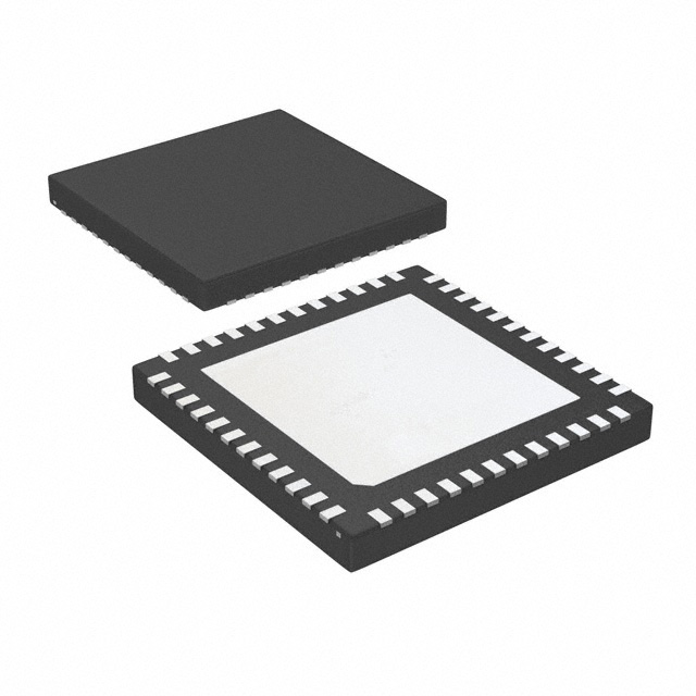
| 描述 | IC CLOCK COND 1.5GHZ W/PLL 48LLP时钟合成器/抖动清除器 Low-Noise Clock Jitter Cleaner with Cascaded PLLs 48-WQFN -40 to 85 |
| 产品分类 | |
| 品牌 | Texas Instruments |
| 产品手册 | |
| 产品图片 |
|
| rohs | 符合RoHS无铅 / 符合限制有害物质指令(RoHS)规范要求 |
| 产品系列 | 时钟和计时器IC,时钟合成器/抖动清除器,Texas Instruments LMK04001BISQE/NOPB- |
| 数据手册 | |
| 产品型号 | LMK04001BISQE/NOPB |
| PLL | 是 |
| 产品目录页面 | |
| 产品种类 | 时钟合成器/抖动清除器 |
| 供应商器件封装 | 48-WQFN(7X7) |
| 其它名称 | *LMK04001BISQE/NOPB |
| 分频器/倍频器 | 是/是 |
| 包装 | 剪切带 (CT) |
| 商标 | Texas Instruments |
| 安装类型 | 表面贴装 |
| 安装风格 | SMD/SMT |
| 封装 | Reel |
| 封装/外壳 | 48-WFQFN 裸露焊盘 |
| 封装/箱体 | WQFN-48 |
| 工作温度 | -40°C ~ 85°C |
| 工厂包装数量 | 250 |
| 差分-输入:输出 | 是/是 |
| 最大工作温度 | + 85 C |
| 最大输入频率 | 400 MHz |
| 最小工作温度 | - 40 C |
| 标准包装 | 1 |
| 比率-输入:输出 | 2:7 |
| 电压-电源 | 3.15 V ~ 3.45 V |
| 电源电压-最大 | 3.45 V |
| 电源电压-最小 | 3.15 V |
| 电源电流 | 380 mA |
| 电路数 | 1 |
| 类型 | 时钟调节器 |
| 系列 | LMK04001 |
| 输入 | LVCMOS,LVDS,LVPECL |
| 输出 | LVCMOS,2VPECL,LVPECL |
| 输出电平 | 2VPECL, LVPECL, LVCMOS |
| 输出端数量 | 3 |
| 频率-最大值 | 1.57GHz |


PDF Datasheet 数据手册内容提取
LMK04000, LMK04001, LMK04002, LMK04010 LMK04011, LMK04031, LMK04033 www.ti.com SNOSAZ8J–SEPTEMBER2008–REVISEDSEPTEMBER2011 LMK04000 Family Low-Noise Clock Jitter Cleaner with Cascaded PLLs CheckforSamples:LMK04000,LMK04001,LMK04002,LMK04010,LMK04011,LMK04031,LMK04033 FEATURES 1 • CascadedPLLatinum™PLLArchitecture • SupportClockRatesupto1080MHz 23 – PLL1 • DefaultClockOutput(CLKout2)atpowerup – PhaseDetectorRateofupto40MHz • FiveDedicatedChannelDividerandDelay – IntegratedLow-NoiseCrystalOscillator Blocks Circuit • PinCompatibleFamilyofClockingDevices – DualRedundantInputReferenceClock • IndustrialTemperatureRange:-40to85°C withLOS • 3.15Vto3.45VOperation – PLL2 • Package:48PinWQFN(7.0x7.0x0.8mm) – Normalized[1Hz]PLLNoiseFloorof- 224dBc/Hz APPLICATIONS – PhaseDetectorRateupto100MHz • DataConverterClocking – InputFrequency-Doubler • WirelessInfrastructure – IntegratedLow-NoiseVCO • Networking,SONET/SDH,DSLAM • Ultra-LowRMSJitterPerformance • Medical – 150fsRMSJitter(12kHz –20MHz) • Military/Aerospace – 200fsRMSJitter(100Hz –20MHz) • TestandMeasurement • LVPECL/2VPECL,LVDS,andLVCMOSoutputs • Video DESCRIPTION The LMK04000 family of precision clock conditioners provides low-noise jitter cleaning, clock multiplication and distribution without the need for high-performance voltage controlled crystal oscillators (VCXO) module. Using a cascaded PLLatinum™ architecture combined with an external crystal and varactor diode, the LMK04000 family providessub-200femtosecond(fs)rootmeansquare(RMS)jitterperformance. The cascaded architecture consists of two high-performance phase-locked loops (PLL), a low-noise crystal oscillatorcircuit,andahigh-performancevoltagecontrolledoscillator(VCO).ThefirstPLL(PLL1)providesalow- noise jitter cleaner function while the second PLL (PLL2) performs the clock generation. PLL1 can be configured to either work with an external VCXO module or use the integrated crystal oscillator with an external crystal and a varactor diode. When used with a very narrow loop bandwidth, PLL1 uses the superior close-in phase noise (offsets below 50 kHz) of the VCXO module or the crystal to clean the input clock. The output of PLL1 is used as the clean input reference to PLL2 where it locks the integrated VCO. The loop bandwidth of PLL2 can be optimized to clean the far-out phase noise (offsets above 50 kHz) where the integrated VCO outperforms the VCXOmoduleorcrystalusedinPLL1. The LMK04000 family features dual redundant inputs, five differential outputs, and an optional default-clock upon power up. The input block is equipped with loss of signal detection and automatic or manual selection of the reference clock. Each clock output consists of a programmable divider, a phase synchronization circuit, a programmabledelay,andanLVDS,LVPECL,orLVCMOSoutputbuffer.Thedefaultstartupclockisavailableon CLKout2 and it can be used to provide an initial clock for the field-programmable gate array (FPGA) or microcontrollerthatprogramsthejittercleanerduringthesystempowerupsequence. 1 Pleasebeawarethatanimportantnoticeconcerningavailability,standardwarranty,anduseincriticalapplicationsof TexasInstrumentssemiconductorproductsanddisclaimerstheretoappearsattheendofthisdatasheet. PLLatinumisatrademarkofTexasInstruments. 2 Allothertrademarksarethepropertyoftheirrespectiveowners. 3 PRODUCTIONDATAinformationiscurrentasofpublicationdate. Copyright©2008–2011,TexasInstrumentsIncorporated Products conform to specifications per the terms of the Texas Instruments standard warranty. Production processing does not necessarilyincludetestingofallparameters.
LMK04000, LMK04001, LMK04002, LMK04010 LMK04011, LMK04031, LMK04033 SNOSAZ8J–SEPTEMBER2008–REVISEDSEPTEMBER2011 www.ti.com Crystal or VCXO Recovered CLKout0 ‡GLUW\·(cid:3)FORFN(cid:3)RU(cid:3) Serializer/ clean clock LMK040xx CLKout1 Deserializer CLKin0 Precision Clock CLKout2A Conditioner LMX2531 CLKin1 CLKout4 PLL+VCO FPGA Fout Backup Reference > 1 Gsps Clock ADC DAC 0XOWLSOH(cid:3)‡FOHDQ·(cid:3)FORFNV(cid:3)DW(cid:3) different frequencies Table1.DeviceConfigurationInformation 2VPECL/LVPECL NSID PROCESS LVDSOUTPUTS LVCMOSOUTPUTS VCO OUTPUTS LMK04000BISQ BiCMOS 3 4 1185to1296MHz LMK04001BISQ BiCMOS 3 4 1430to1570MHz LMK04002BISQ BiCMOS 3 4 1600to1750MHz LMK04010BISQ BiCMOS 5 1185to1296MHz LMK04011BISQ BiCMOS 5 1430to1570MHz LMK04031BISQ BiCMOS 2 2 2 1430to1570MHz LMK04033BISQ BiCMOS 2 2 2 1840to2160MHz NSID CLKout0 CLKout1 CLKout2 CLKout3 CLKout4 LMK04000BISQ 2VPECL/LVPECL LVCMOSx2 LVCMOSx2 2VPECL/LVPECL 2VPECL/LVPECL LMK04001BISQ 2VPECL/LVPECL LVCMOSx2 LVCMOSx2 2VPECL/LVPECL 2VPECL/LVPECL LMK04002BISQ 2VPECL/LVPECL LVCMOSx2 LVCMOSx2 2VPECL/LVPECL 2VPECL/LVPECL LMK04010BISQ 2VPECL/LVPECL 2VPECL/LVPECL 2VPECL/LVPECL 2VPECL/LVPECL 2VPECL/LVPECL LMK04011BISQ 2VPECL/LVPECL 2VPECL/LVPECL 2VPECL/LVPECL 2VPECL/LVPECL 2VPECL/LVPECL LMK04031BISQ LVDS 2VPECL/LVPECL LVCMOSx2 2VPECL/LVPECL LVDS LMK04033BISQ LVDS 2VPECL/LVPECL LVCMOSx2 2VPECL/LVPECL LVDS 2 SubmitDocumentationFeedback Copyright©2008–2011,TexasInstrumentsIncorporated ProductFolderLinks:LMK04000 LMK04001 LMK04002 LMK04010LMK04011 LMK04031 LMK04033
LMK04000, LMK04001, LMK04002, LMK04010 LMK04011, LMK04031, LMK04033 www.ti.com SNOSAZ8J–SEPTEMBER2008–REVISEDSEPTEMBER2011 Functional Block Diagram LOS0 LOS ut1 Po C CLKin0 CLKin0* Mux R1 Divider Phase CLKin1 Detector CLKin1* N1 Divider PLL1 LOS1 LOS 2 ut 2X Po Partially Mux C Integrated OSCin R2 Divider Loop Filter Internal VCO OSCin* Phase Detector Fout N2 Divider PLL2 VCO Divider Distribution Path CLKout4 Divider Mux Delay CLKout4* GOE Device LD CLKout3B SYNC* Control Divider Delay Mux CLKout3A CLK CLKout2B DATA PPWoirrte RCeognisttreorls Divider Delay Mux CLKout2A LE CLKout1 Divider Mux Delay CLKout1* CLKout0 Divider Mux Delay CLKout0* Clock Buffers Copyright©2008–2011,TexasInstrumentsIncorporated SubmitDocumentationFeedback 3 ProductFolderLinks:LMK04000 LMK04001 LMK04002 LMK04010LMK04011 LMK04031 LMK04033
LMK04000, LMK04001, LMK04002, LMK04010 LMK04011, LMK04031, LMK04033 SNOSAZ8J–SEPTEMBER2008–REVISEDSEPTEMBER2011 www.ti.com Connection Diagram 4* 4 3* 3 2* 2 1* 1 CLKout CLKout Vcc14 CLKout CLKout Vcc13 CLKout CLKout Vcc12 CLKout CLKout Vcc11 48 47 46 45 44 43 42 41 40 39 38 37 GND 1 36 Bias Fout 2 35 CLKin1_LOS Vcc1 3 34 CLKin0_LOS CLKuWire 4 33 Vcc10 DATAuWire 5 32 CPout2 LEuWire 6 31 Vcc9 NC 7 30 Vcc8 Vcc2 8 29 OSCin* LDObyp1 9 28 OSCin LDObyp2 10 27 SYNC* DAP GOE 11 26 CLKin1* LD 12 25 CLKin1 13 14 15 16 17 18 19 20 21 22 23 24 Vcc3 CLKout0 CLKout0* DLD_BYP GND Vcc4 Vcc5 CLKin0 CLKin0* Vcc6 CPout1 Vcc7 Figure1. 48-PinWQFNPackage TopView PINDESCRIPTIONS PinNumber Name(s) I/O Type Description 1 GND GND Ground(ForFoutBuffer) 2 Fout O ANLG VCOFrequencyOutputPort 3 V 1 PWR PowerSupplyforVCOOutputBuffer CC 4 CLKuWire I CMOS MicrowireClockInput 5 DATAuWire I CMOS MicrowireDataInput 6 LEuWire I CMOS MicrowireLatchEnableInput 7 NC NoConnection 8 V 2 PWR PowerSupplyforVCO CC 9 LDObyp1 ANLG LDOBypass,bypassedtogroundwitha10µFcapacitor 10 LDObyp2 ANLG LDOBypass,bypassedtogroundwitha0.1µF capacitor 11 GOE I CMOS GlobalOutputEnable 12 LD O CMOS LockDetectandPLLmultiplexerOutput 13 V 3 PWR PowerSupplyforCLKout0 CC 14 CLKout0 O LVDS/LVPECL ClockChannel0Output 15 CLKout0* O LVDS/LVPECL ClockChannel0*Output 16 DLD_BYP ANLG DLDBypass,bypassedtogroundwitha0.47µF capacitor 17 GND GND Ground(Digital) 18 V 4 PWR PowerSupplyforDigital CC 4 SubmitDocumentationFeedback Copyright©2008–2011,TexasInstrumentsIncorporated ProductFolderLinks:LMK04000 LMK04001 LMK04002 LMK04010LMK04011 LMK04031 LMK04033
LMK04000, LMK04001, LMK04002, LMK04010 LMK04011, LMK04031, LMK04033 www.ti.com SNOSAZ8J–SEPTEMBER2008–REVISEDSEPTEMBER2011 PINDESCRIPTIONS(continued) PinNumber Name(s) I/O Type Description 19 V 5 PWR PowerSupplyforCLKinbuffersandPLL1R-divider CC 20 CLKin0 I ANLG ReferenceClockInputPortforPLL1-ACorDC Coupled (1) 21 CLKin0* I ANLG ReferenceClockInputPortforPLL1(complimentary)- ACorDCCoupled (1) 22 V 6 PWR PowerSupplyforPLL1PhaseDetectorandCharge CC Pump 23 CPout1 O ANLG ChargePump1Output 24 V 7 PWR PowerSupplyforPLL1N-Divider CC 25 CLKin1 I ANLG ReferenceClockInputPortforPLL1-ACorDC Coupled (1) 26 CLKin1* I ANLG ReferenceClockInputPortforPLL1(complimentary)- ACorDCCoupled (1) 27 SYNC* I CMOS GlobalClockOutputSynchronization 28 OSCin I ANLG ReferenceoscillatorInputforPLL2-ACCoupled 29 OSCin* I ANLG ReferenceoscillatorInputforPLL2-ACCoupled 30 V 8 PWR PowerSupplyforOSCinBufferandPLL2R-Divider CC 31 V 9 PWR PowerSupplyforPLL2PhaseDetectorandCharge CC Pump 32 CPout2 O ANLG ChargePump2Output 33 V 10 PWR PowerSupplyforVCODividerandPLL2N-Divider CC 34 CLKin0_LOS O LVCMOS StatusofCLKin0referenceclockinput 35 CLKin1_LOS O LVCMOS StatusofCLKin1referenceclockinput 36 Bias I ANLG BiasBypass.ACcoupledwith1µFcapacitortoVcc1 37 V 11 PWR PowerSupplyforCLKout1 CC 38 CLKout1 O LVPECL/LVCMOS ClockChannel1Output 39 CLKout1* O LVPECL/LVCMOS ClockChannel1*Output 40 V 12 PWR PowerSupplyforCLKout2 CC 41 CLKout2 O LVPECL/LVCMOS ClockChannel2Output 42 CLKout2* O LVPECL/LVCMOS ClockChannel2*Output 43 V 13 PWR PowerSupplyforCLKout3 CC 44 CLKout3 O LVPECL ClockChannel3Output 45 CLKout3* O LVPECL ClockChannel3*Output 46 V 14 PWR PowerSupplyforCLKout4 CC 47 CLKout4 O LVDS/LVPECL ClockChannel4Output 48 CLKout4* O LVDS/LVPECL ClockChannel4*Output DAP DAP DIEATTACHPAD,connecttoGND (1) ThereferenceclockinputsmaybeeitherACorDCcoupled. Thesedeviceshavelimitedbuilt-inESDprotection.Theleadsshouldbeshortedtogetherorthedeviceplacedinconductivefoam duringstorageorhandlingtopreventelectrostaticdamagetotheMOSgates. Copyright©2008–2011,TexasInstrumentsIncorporated SubmitDocumentationFeedback 5 ProductFolderLinks:LMK04000 LMK04001 LMK04002 LMK04010LMK04011 LMK04031 LMK04033
LMK04000, LMK04001, LMK04002, LMK04010 LMK04011, LMK04031, LMK04033 SNOSAZ8J–SEPTEMBER2008–REVISEDSEPTEMBER2011 www.ti.com Absolute Maximum Ratings(1)(2)(3)(4) Parameter Symbol Ratings Units SupplyVoltage (5) V -0.3to3.6 V CC InputVoltage V -0.3to(V +0.3) V IN CC StorageTemperatureRange T -65to150 °C STG LeadTemperature(solder4sec) T +260 °C L DifferentialInputCurrent(CLKinX/X*, I ±5 mA OSCin/OSCin*) IN (1) "AbsoluteMaximumRatings"indicatelimitsbeyondwhichdamagetothedevicemayoccur.OperatingRatingsindicateconditionsfor whichthedeviceisintendedtobefunctional,butdonotguaranteespecificperformancelimits.Forguaranteedspecificationsandtest conditions,seetheElectricalCharacteristics.Theguaranteedspecificationsapplyonlytothetestconditionslisted. (2) IfMilitary/Aerospacespecifieddevicesarerequired,pleasecontacttheTISalesOffice/Distributorsforavailabilityandspecifications. (3) ThisdeviceisahighperformanceRFintegratedcircuitwithanESDratingupto8KVHumanBodyModel,upto300VMachineModel andupto1,250VChargedDeviceModelandisESDsensitive.HandlingandassemblyofthisdeviceshouldonlybedoneatESD-free workstations. (4) Stressesinexcessoftheabsolutemaximumratingscancausepermanentorlatentdamagetothedevice.Theseareabsolutestress ratingsonly.Functionaloperationofthedeviceisonlyimpliedattheseoranyotherconditionsinexcessofthosegivenintheoperation sectionsofthedatasheet.Exposuretoabsolutemaximumratingsforextendedperiodscanadverselyaffectdevicereliability. (5) Nevertoexceed3.6V. Package Thermal Resistance Package θ θ JA J-PAD(ThermalPad) 48-LeadWQFN (1) 27.4°C/W 5.8°C/W (1) Specificationassumes16thermalviasconnectthedieattachpadtotheembeddedcopperplaneonthe4-layerJEDECboard.These viasplayakeyroleinimprovingthethermalperformanceoftheWQFN.Itisrecommendedthatthemaximumnumberofviasbeusedin theboardlayout. Recommended Operating Conditions Parameter Symbol Condition Min Typical Max Unit Ambient T V =3.3V -40 25 85 °C Temperature A CC SupplyVoltage V 3.15 3.3 3.45 V CC Electrical Characteristics (3.15V≤V ≤3.45V,-40°C≤T ≤85°C.TypicalvaluesrepresentmostlikelyparametricnormsatV =3.3V,T =25 CC A CC A °C,attheRecommendedOperatingConditionsatthetimeofproductcharacterizationandarenotguaranteed.) Symbol Parameter Conditions Min Typ Max Units CurrentConsumption I PowerDownSupplyCurrent 1 mA CC_PD LMK04000,LMK04001, LMK04002 380 435 (2) SupplyCurrentwithallclocks I enabled,alldelaybypassed, LMK04010,LMK04011 mA CC_CLKS Foutdisabled. (1) (2) 378 435 LMK04031,LMK04033 (2) 335 385 CLKin0/0*andCLKin1/1*InputClockSpecifications ClockInputFrequency ManualSelectmode 0.001 400 fCLKin (3) MHz Auto-Switchingmode 1 400 (1) Loadconditionsforoutputclocks:LVPECL:50ΩtoV -2V.2VPECL:50ΩtoV -2.36V.LVDS:100Ωdifferential.LVCMOS:10pF. CC CC (2) AdditionaltestconditionsforI limits:Allclockdelaysdisabled,CLKoutX_DIV=510,PLL1andPLL2locked.(SeeTable33formore CC information) (3) CLKin0andCLKin1maximumof400MHzisguaranteedbycharacterization,productiontestedat200MHz. 6 SubmitDocumentationFeedback Copyright©2008–2011,TexasInstrumentsIncorporated ProductFolderLinks:LMK04000 LMK04001 LMK04002 LMK04010LMK04011 LMK04031 LMK04033
LMK04000, LMK04001, LMK04002, LMK04010 LMK04011, LMK04031, LMK04033 www.ti.com SNOSAZ8J–SEPTEMBER2008–REVISEDSEPTEMBER2011 Electrical Characteristics (continued) (3.15V≤V ≤3.45V,-40°C≤T ≤85°C.TypicalvaluesrepresentmostlikelyparametricnormsatV =3.3V,T =25 CC A CC A °C,attheRecommendedOperatingConditionsatthetimeofproductcharacterizationandarenotguaranteed.) Symbol Parameter Conditions Min Typ Max Units SlewRateonCLKin SLEWCLKin (4) 20%to80% 0.15 0.5 V/ns ACcoupledtoCLKinX; InputVoltageSwing, CLKinX*ACcoupledtoGround 0.25 2.0 Vpp single-endedinput V (Bipolarinputbuffer (CLKinX_TYPE=0) CLKin mode) CLKinXandCLKinX*areboth InputVoltageSwing, driven,ACcoupled. 0.5 3.1 Vpp differentialinput (CLKinX_TYPE=0) DCoffsetvoltagebetween V (Bipolarinput EachpinACcoupled CLKin-offset CLKinX/CLKinX* 44 mV buffermode) (CLKinX_TYPE=0) |CLKinX-CLKinX*| ACcoupledtoCLKinX; InputVoltageSwing,single- CLKinX*ACcoupledtoGround 0.25 2.0 Vpp endedinput V (MOSinputbuffer (CLKinX_TYPE=1) CLKin mode) CLKinXandCLKinX*areboth InputVoltageSwing, driven,ACcoupled. 0.5 3.1 Vpp differentialinput (CLKinX_TYPE=1) DCcoupledtoCLKinX; V V (MOSinputbuffer CLKin- IH Maximuminputvoltage CLKinX*ACcoupledtoGround 2.0 V V mode) CC (CLKinX_TYPE=1) DCcoupledtoCLKinX; V V (MOSinputbuffer CLKin- IL CLKinX*ACcoupledtoGround 0.0 0.4 V mode) (CLKinX_TYPE=1) DCoffsetvoltagebetween V (MOSinput EachpinACcoupled CLKin-offset CLKinX/CLKinX* 294 mV buffermode) (CLKinX_TYPE=1) |CLKinX-CLKinX*| PLL1Specifications PLL1PhaseDetector f 40 MHz PD Frequency V =V /2, CPout1 CC 25 PLL1_CP_GAIN=100b V =V /2, CPout1 CC 50 PLL1_CP_GAIN=101b V =V /2, CPout1 CC 100 PLL1_CP_GAIN=110b ICPout1SOURCE PCLuLrr1enCth(a5)rgePumpSource VPCLPLo1u_t1C=P_VGCCA/I2N,=111b 400 µA PLL1_CP_GAIN=000b NA PLL1_CP_GAIN=001b NA V =V /2,PLL1_CP_GAIN CPout1 CC 20 =010b V =V /2,PLL1_CP_GAIN CPout1 CC 80 =011b (4) Inordertomeetthejitterperformancelistedinthesubsequentsectionsofthisdatasheet,theminimumrecommendedslewrateforall inputclocksis0.5V/ns.Thisisespeciallytrueforsingle-endedclocks.Phasenoiseperformancewillbegintodegradeastheclockinput slewrateisreduced.However,thedevicewillfunctionatslewratesdowntotheminimumlisted.Whencomparedtosingle-ended clocks,differentialclocks(LVDS,LVPECL)willbelesssusceptibletodegradationinphasenoiseperformanceatlowerslewratesdueto theircommonmodenoiserejection.However,itisalsorecommendedtousethehighestpossibleslewratefordifferentialclocksto achieveoptimalphasenoiseperformanceatthedeviceoutputs. (5) Thisparameterisprogrammable Copyright©2008–2011,TexasInstrumentsIncorporated SubmitDocumentationFeedback 7 ProductFolderLinks:LMK04000 LMK04001 LMK04002 LMK04010LMK04011 LMK04031 LMK04033
LMK04000, LMK04001, LMK04002, LMK04010 LMK04011, LMK04031, LMK04033 SNOSAZ8J–SEPTEMBER2008–REVISEDSEPTEMBER2011 www.ti.com Electrical Characteristics (continued) (3.15V≤V ≤3.45V,-40°C≤T ≤85°C.TypicalvaluesrepresentmostlikelyparametricnormsatV =3.3V,T =25 CC A CC A °C,attheRecommendedOperatingConditionsatthetimeofproductcharacterizationandarenotguaranteed.) Symbol Parameter Conditions Min Typ Max Units V =V /2,PLL1_CP_GAIN CPout1 CC -25 =100b V =V /2,PLL1_CP_GAIN CPout1 CC -50 =101b V =V /2,PLL1_CP_GAIN CPout1 CC -100 =110b ICPout1SINK PCLuLrr1enCth(a5)rgePumpSink V=C1P1o1utb1=VCC/2,PLL1_CP_GAIN -400 µA PLL1_CP_GAIN=000b NA PLL1_CP_GAIN=001b NA V =V /2,PLL1_CP_GAIN CPout1 CC -20 =010b V =V /2,PLL1_CP_GAIN CPout1 CC -80 =011b ChargePumpSink/Source I %MIS V =V /2,T=25°C 3 10 % CPout1 Mismatch CPout1 CC MagnitudeofChargePump 0.5V<V <V -0.5V I V Currentvs.ChargePump CPout1 CC 4 % CPout1 TUNE T =25°C VoltageVariation A ChargePumpCurrentvs. I %TEMP 4 % CPout1 TemperatureVariation ChargePumpTRI-STATE PLL1I TRI 0.5V<V <V -0.5V 5 nA CPout1 LeakageCurrent CPout CC PLL2ReferenceInput(OSCin)Specifications EN_PLL2_REF2X=0 PLL2ReferenceInput (7) 250 fOSCin (6) MHz EN_PLL2_REF2X=1 50 PLL2ReferenceClock SLEW 20%to80% 0.15 0.5 V/ns OSCin minimumslewrateonOSCin ACcoupled;Single-ended InputVoltageforOSCinor V (Single-ended) (UnusedpinACcoupledto 0.2 2.0 Vpp OSCin OSCin* GND) V (Differential) Differentialvoltageswing ACcoupled 0.4 3.1 Vpp OSCin CrystalOscillatorModeSpecifications f CrystalFrequencyRange 6 20 MHz XTAL CrystalEffectiveSeries ESR 6MHz<F <20MHz 100 Ohms Resistance XTAL P CrystalPowerDissipation (8) VectronVXB1crystal,12.288 200 µW XTAL MHz,R <40Ω ESR InputCapacitanceof C -40to+85°C 6 pF IN LMK040xxOSCinport PLL2PhaseDetectorandChargePumpSpecifications f PhaseDetectorFrequency 100 MHz PD (6) F maximumfrequencyguaranteedbycharacterization.Productiontestedat200MHz. OSCin (7) TheEN_PLL2_REF2Xbit(Register13)enables/disablesafrequencydoublermodeforthePLL2OSCinpath. (8) SeeApplicationSectiondiscussionofCrystalPowerDissipation. 8 SubmitDocumentationFeedback Copyright©2008–2011,TexasInstrumentsIncorporated ProductFolderLinks:LMK04000 LMK04001 LMK04002 LMK04010LMK04011 LMK04031 LMK04033
LMK04000, LMK04001, LMK04002, LMK04010 LMK04011, LMK04031, LMK04033 www.ti.com SNOSAZ8J–SEPTEMBER2008–REVISEDSEPTEMBER2011 Electrical Characteristics (continued) (3.15V≤V ≤3.45V,-40°C≤T ≤85°C.TypicalvaluesrepresentmostlikelyparametricnormsatV =3.3V,T =25 CC A CC A °C,attheRecommendedOperatingConditionsatthetimeofproductcharacterizationandarenotguaranteed.) Symbol Parameter Conditions Min Typ Max Units V =V /2,PLL2_CP_GAIN CPout2 CC 100 =00b V =V /2,PLL2_CP_GAIN CPout2 CC 400 PLL2ChargePumpSource =01b ICPoutSOURCE Current (9) V =V /2,PLL2_CP_GAIN µA CPout2 CC 1600 =10b V =V /2,PLL2_CP_GAIN CPout2 CC 3200 =11b V =V /2,PLL2_CP_GAIN CPout2 CC -100 =00b V =V /2,PLL2_CP_GAIN CPout2 CC -400 PLL2ChargePumpSink =01b ICPoutSINK Current (9) V =V /2,PLL2_CP_GAIN µA CPout2 CC -1600 =10b V =V /2,PLL2_CP_GAIN CPout2 CC -3200 =11b ChargePumpSink/Source I %MIS V =V /2,T =25°C 3 10 % CPout2 Mismatch CPout2 CC A MagnitudeofChargePump 0.5V<V <V -0.5V I V Currentvs.ChargePump CPout2 CC 4 % CPout2 TUNE T =25°C VoltageVariation A ChargePumpCurrentvs. I %TEMP 4 % CPout2 TemperatureVariation I TRI ChargePumpLeakage 0.5V<V <V -0.5V 10 nA CPout2 CPout2 CC PLL1/fNoiseat10kHzoffset PLL2_CP_GAIN=400µA -117 PN10kHz (10).Normalizedto dBc/Hz 1GHzOutputFrequency PLL2_CP_GAIN=3200µA -122 NormalizedPhaseNoise PLL2_CP_GAIN=400µA -219 PN1Hz Contribution (11) PLL2_CP_GAIN=3200µA -224 dBc/Hz InternalVCOSpecifications LMK040x0 1185 1296 LMK040x1 1430 1570 f VCOTuningRange MHz VCO LMK040x2 1600 1750 LMK040x3 1840 2160 LMK040x0,T =25°C,single- A 3 ended LMK040x1,T =25°C,single- A 3 ended VCOOutputpowertoa LMK040x2,T =25°C,single- P A 2 dBm VCO 50ΩloaddrivenbyFout ended LMK040x3,T =25°C,single- A 0 ended1840MHz LMK040x3,T =25°C,single- A -5 ended2160MHz (9) Thisparameterisprogrammable (10) AspecificationinmodelingPLLin-bandphasenoiseisthe1/fflickernoise,L (f),whichisdominantclosetothecarrier.Flicker PLL_flicker noisehasa10dB/decadeslope.PN10kHzisnormalizedtoa10kHzoffsetanda1GHzcarrierfrequency.PN10kHz=L (10 PLL_flicker kHz)-20log(Fout/1GHz),whereL (f)isthesinglesidebandphasenoiseofonlytheflickernoise'scontributiontototalnoise, PLL_flicker L(f).TomeasureL (f)itisimportanttobeonthe10dB/decadeslopeclosetothecarrier.Ahighcomparefrequencyandaclean PLL_flicker crystalareimportanttoisolatingthisnoisesourcefromthetotalphasenoise,L(f).L (f)canbemaskedbythereference PLL_flicker oscillatorperformanceifalowpowerornoisysourceisused.ThetotalPLLinbandphasenoiseperformanceisthesumofL (f) PLL_flicker andL (f). PLL_flat (11) AspecificationmodelingPLLin-bandphasenoise.ThenormalizedphasenoisecontributionofthePLL,L (f),isdefinedas: PLL_flat PN1HZ=L (f)-20log(N)-10log(f ).L (f)isthesinglesidebandphasenoisemeasuredatanoffsetfrequency,f,ina1Hz PLL_flat COMP PLL_flat bandwidthandf isthephasedetectorfrequencyofthesynthesizer.L (f)contributestothetotalnoise,L(f). COMP PLL_flat Copyright©2008–2011,TexasInstrumentsIncorporated SubmitDocumentationFeedback 9 ProductFolderLinks:LMK04000 LMK04001 LMK04002 LMK04010LMK04011 LMK04031 LMK04033
LMK04000, LMK04001, LMK04002, LMK04010 LMK04011, LMK04031, LMK04033 SNOSAZ8J–SEPTEMBER2008–REVISEDSEPTEMBER2011 www.ti.com Electrical Characteristics (continued) (3.15V≤V ≤3.45V,-40°C≤T ≤85°C.TypicalvaluesrepresentmostlikelyparametricnormsatV =3.3V,T =25 CC A CC A °C,attheRecommendedOperatingConditionsatthetimeofproductcharacterizationandarenotguaranteed.) Symbol Parameter Conditions Min Typ Max Units FineTuningSensitivity LMK040x0 7to9 (Therangedisplayedinthe LMK040x1 8to11 typicalcolumnindicatesthe lowersensitivityistypicalat LMK040x2 9to14 K thelowerendofthetuning MHz/V VCO range,andthehighertuning sensitivityistypicalatthe LMK040x3 14to26 higherendofthetuning range). AfterprogrammingR15for AllowableTemperatureDrift lock,nochangestooutput |ΔT | forContinuousLock 125 °C CL (12) configurationarepermittedto guaranteecontinuouslock InternalVCOOpenLoopPhaseNoiseandJitter Offset=1kHz -66 LMK040x0 Offset=10kHz -94 fVCO=1185MHz Offset=100kHz -119 SSBPhaseNoise dBc/Hz PLL2=OpenLoop Offset=1MHz -139 MeasuredatFout Offset=10MHz -158 Offset=20MHz -163 Offset=1kHz -64 LMK040x0 Offset=10kHz -91 fVCO=1296MHz Offset=100kHz -117 SSBPhaseNoise dBc/Hz PLL2=OpenLoop Offset=1MHz -138 MeasuredatFout Offset=10MHz -157 Offset=20MHz -161 L(f) Fout Offset=1kHz -61 LMK040x1 Offset=10kHz -91 fVCO=1440MHz Offset=100kHz -117 SSBPhaseNoise dBc/Hz PLL2=OpenLoop Offset=1MHz -138 MeasuredatFout Offset=10MHz -158 Offset=20MHz -160 Offset=1kHz -58 LMK040x1 Offset=10kHz -89 fVCO=1560MHz Offset=100kHz -115 SSBPhaseNoise dBc/Hz PLL2=OpenLoop Offset=1MHz -137 MeasuredatFout Offset=10MHz -157 Offset=20MHz -162 (12) MaximumAllowableTemperatureDriftforContinuousLockishowfarthetemperaturecandriftineitherdirectionfromthevalueitwas atthetimethattheR0registerwaslastprogrammed,andstillhavethepartstayinlock.TheactionofprogrammingtheR0register, eventothesamevalue,activatesafrequencycalibrationroutine.Thisimpliesthepartwillworkovertheentirefrequencyrange,butif thetemperaturedriftsmorethanthemaximumallowabledriftforcontinuouslock,thenitwillbenecessarytoreloadtheR0registerto ensureitstaysinlock.Regardlessofwhattemperaturethepartwasinitiallyprogrammedat,thetemperaturecanneverdriftoutsidethe frequencyrangeof-40°Cto85°Cwithoutviolatingspecifications. 10 SubmitDocumentationFeedback Copyright©2008–2011,TexasInstrumentsIncorporated ProductFolderLinks:LMK04000 LMK04001 LMK04002 LMK04010LMK04011 LMK04031 LMK04033
LMK04000, LMK04001, LMK04002, LMK04010 LMK04011, LMK04031, LMK04033 www.ti.com SNOSAZ8J–SEPTEMBER2008–REVISEDSEPTEMBER2011 Electrical Characteristics (continued) (3.15V≤V ≤3.45V,-40°C≤T ≤85°C.TypicalvaluesrepresentmostlikelyparametricnormsatV =3.3V,T =25 CC A CC A °C,attheRecommendedOperatingConditionsatthetimeofproductcharacterizationandarenotguaranteed.) Symbol Parameter Conditions Min Typ Max Units Offset=1kHz -63 LMK040x2 Offset=10kHz -91 fVCO=1600MHz Offset=100kHz -115 SSBPhaseNoise dBc/Hz PLL2=OpenLoop Offset=1MHz -137 MeasuredatFout Offset=10MHz -156 Offset=20MHz -161 Offset=1kHz -61 LMK040x2 Offset=10kHz -90 fVCO=1750MHz Offset=100kHz -114 SSBPhaseNoise dBc/Hz PLL2=OpenLoop Offset=1MHz -136 MeasuredatFout Offset=10MHz -155 Offset=20MHz -160 L(f) Fout Offset=1kHz -58 LMK040x3 Offset=10kHz -88 fVCO=1840MHz Offset=100kHz -113 SSBPhaseNoise dBc/Hz PLL2=OpenLoop Offset=1MHz -135 MeasuredatFout Offset=10MHz -155 Offset=20MHz -158 Offset=1kHz -54 LMK040x3 Offset=10kHz -84 fVCO=2160MHz Offset=100kHz -110 SSBPhaseNoise dBc/Hz PLL2=OpenLoop Offset=1MHz -132 MeasuredatFout Offset=10MHz -154 Offset=20MHz -157 Copyright©2008–2011,TexasInstrumentsIncorporated SubmitDocumentationFeedback 11 ProductFolderLinks:LMK04000 LMK04001 LMK04002 LMK04010LMK04011 LMK04031 LMK04033
LMK04000, LMK04001, LMK04002, LMK04010 LMK04011, LMK04031, LMK04033 SNOSAZ8J–SEPTEMBER2008–REVISEDSEPTEMBER2011 www.ti.com Electrical Characteristics (continued) (3.15V≤V ≤3.45V,-40°C≤T ≤85°C.TypicalvaluesrepresentmostlikelyparametricnormsatV =3.3V,T =25 CC A CC A °C,attheRecommendedOperatingConditionsatthetimeofproductcharacterizationandarenotguaranteed.) Symbol Parameter Conditions Min Typ Max Units InternalVCOClosedLoopPhaseNoiseandJitterSpecificationsusinganInstrumentationQualityVCXO Offset=1kHz -111 Offset=10kHz -119 LMK040x0 (13) Offset=100kHz -121 f =1200MHz VCO SSBPhaseNoise Offset=1MHz -133 dBc/Hz PLL2=ClosedLoop Offset=10MHz -157 MeasuredatFout Offset=20MHz -162 Offset=40MHz -165 Offset=1kHz -110 Offset=10kHz -117 LMK040x1 (14) Offset=100kHz -120 f =1500MHz VCO SSBPhaseNoise Offset=1MHz -132 dBc/Hz PLL2=ClosedLoop Offset=10MHz -156 MeasuredatFout Offset=20MHz -160 Offset=40MHz -163 L(f) Fout Offset=1kHz -111 Offset=10kHz -118 LMK040x2 (15) Offset=100kHz -120 f =1600MHz VCO SSBPhaseNoise Offset=1MHz -132 dBc/Hz PLL2=ClosedLoop Offset=10MHz -156 MeasuredatFout Offset=20MHz -162 Offset=40MHz -165 Offset=1kHz -107 Offset=10kHz -114 LMK040x3 (16) Offset=100kHz -117 f =2000MHz VCO SSBPhaseNoise Offset=1MHz -126 dBc/Hz PLL2=ClosedLoop Offset=10MHz -152 MeasuredatFout Offset=20MHz -156 Offset=40MHz -160 (13) ForLMK040x0,f =1200MHz.PLL1ispowereddown.A100MHzWenzelXO(model:501-04623G)drivestheOSCininputof VCO PLL2.PLL2parameters:VCO_DIV=3,N2=5,R2=1,F =100MHz,ICP2=1.6mA,C1=22pF,C2=5.6nF,R2=1.8kΩ,LBW= DET 268kHz,PM=75°.WenzelXOphasenoise:100Hz:-132dBc/Hz;1kHz:-147dBc/Hz;10kHz:-159dBc/Hz;100kHz:-167dBc/Hz. (14) ForLMK040x1,f =1500MHz.PLL1ispowereddown.A100MHzWenzelXO(model:501-04623G)drivestheOSCininputof VCO PLL2.PLL2parameters:VCO_DIV=3,N2=5,R2=1,F =100MHz,ICP2=1.6mA,C1=22pF,C2=5.6nF,R2=1.8kΩ,LBW= DET 268kHz,PM=75°.WenzelXOphasenoise:100Hz:-132dBc/Hz;1kHz:-147dBc/Hz;10kHz:-159dBc/Hz;100kHz:-167dBc/Hz. (15) ForLMK040x2,f =1600MHz.PLL1ispowereddown.A100MHzWenzelXO(model:501-04623G)drivestheOSCininputof VCO PLL2.PLL2parameters:VCO_DIV=2,N2=8,R2=1,F =100MHz,ICP2=1.6mA,C1=22pF,C2=5.6nF,R2=1.8kΩ,LBW= DET 252kHz,PM=76°.WenzelXOphasenoise:100Hz:-132dBc/Hz;1kHz:-147dBc/Hz;10kHz:-159dBc/Hz;100kHz:-167dBc/Hz. (16) ForLMK040x3,f =2000MHz.PLL1ispowereddown.A100MHzWenzelXO(model:501-04623G)drivestheOSCininputof VCO PLL2.PLL2parameters:VCO_DIV=2,N2=10,R2=1,F =100MHz,ICP2=1.6mA,C1=22pF,C2=5.6nF,R2=1.8kΩ,LBW DET =434kHz,PM=69°.WenzelXOphasenoise:100Hz:-132dBc/Hz;1kHz:-147dBc/Hz;10kHz:-159dBc/Hz;100kHz:-167dBc/Hz. 12 SubmitDocumentationFeedback Copyright©2008–2011,TexasInstrumentsIncorporated ProductFolderLinks:LMK04000 LMK04001 LMK04002 LMK04010LMK04011 LMK04031 LMK04033
LMK04000, LMK04001, LMK04002, LMK04010 LMK04011, LMK04031, LMK04033 www.ti.com SNOSAZ8J–SEPTEMBER2008–REVISEDSEPTEMBER2011 Electrical Characteristics (continued) (3.15V≤V ≤3.45V,-40°C≤T ≤85°C.TypicalvaluesrepresentmostlikelyparametricnormsatV =3.3V,T =25 CC A CC A °C,attheRecommendedOperatingConditionsatthetimeofproductcharacterizationandarenotguaranteed.) Symbol Parameter Conditions Min Typ Max Units LMK040x0 (13) BW=12kHzto20MHz 105 f =1200MHz VCO IntegratedRMSJitter BW=100Hzto20MHz 110 LMK040x1 (14) BW=12kHzto20MHz 100 f =1500MHz VCO IntegratedRMSJitter BW=100Hzto20MHz 105 J fs Fout LMK040x2 (15) BW=12kHzto20MHz 95 f =1600MHz VCO IntegratedRMSJitter BW=100Hzto20MHz 100 LMK040x3 (16) BW=12kHzto20MHz 105 f =2000MHz VCO IntegratedRMSJitter BW=100Hzto20MHz 110 CLKout'sInternalVCOClosedLoopPhaseNoiseandJitterSpecificationsusinganInstrumentationQualityVCXO LMK040x0 (17) Offset=1kHz -125 fCLKout=250MHz Offset=10kHz -130 SSBPhaseNoise Offset=100kHz -132 MeasuredatClockOutputs Valueisaverageforalloutput Offset=1MHz -148 types Offset=10MHz -157 LMK040x1 (18) Offset=1kHz -126 fCLKout=250MHz Offset=10kHz -133 SSBPhaseNoise Offset=100kHz -136 MeasuredatClockOutputs Valueisaverageforalloutput Offset=1MHz -147 types Offset=10MHz -156 L(f) dBc/Hz CLKout LMK040x2 (19) Offset=1kHz -127 fCLKout=250MHz Offset=10kHz -133 SSBPhaseNoise Offset=100kHz -134 MeasuredatClockOutputs Valueisaverageforalloutput Offset=1MHz -145 types Offset=10MHz -157 LMK040x3 (20) Offset=1kHz -125 fCLKout=250MHz Offset=10kHz -132 SSBPhaseNoise Offset=100kHz -135 MeasuredatClockOutputs ValueIsaverageforalloutput Offset=1MHz -145 types Offset=10MHz -156 (17) ForLMK040x0,f =1250MHz.PLL1ispowereddown.A100MHzWenzelXO(model:501-04623G)drivestheOSCininputof VCO PLL2.PLL2parameters:VCO_DIV=5,N2=5,R2=2,F =50MHz,ICP2=3.2mA,C1=22pF,C2=5.6nF,R2=1.8kΩ,LBW= DET 251kHz,PM=76°.WenzelXOphasenoise:100Hz:-132dBc/Hz;1kHz:-147dBc/Hz;10kHz:-159dBc/Hz;100kHz:-167dBc/Hz. CLKoutX_DIV=Bypass.CLKout_DLY=OFF. (18) ForLMK040x1,f =1500MHz.PLL1ispowereddown.A100MHzWenzelXO(model:501-04623G)drivestheOSCininputof VCO PLL2.PLL2parameters:VCO_DIV=3,N2=5,R2=1,F =100MHz,ICP2=1.6mA,C1=22pF,C2=5.6nF,R2=1.8kΩ,LBW= DET 268kHz,PM=75°.WenzelXOphasenoise:100Hz:-132dBc/Hz;1kHz:-147dBc/Hz;10kHz:-159dBc/Hz;100kHz:-167dBc/Hz. CLKoutX_DIV=2.CLKout_DLY=OFF. (19) ForLMK040x2,f =1750MHz.PLL1ispowereddown.A100MHzWenzelXO(model:501-04623G)drivestheOSCininputof VCO PLL2.PLL2parameters:VCO_DIV=7,N2=5,R2=2,F =50MHz,ICP2=1.6mA,C1=22pF,C2=5.6nF,R2=1.8kΩ,LBW= DET 354kHz,PM=73°.WenzelXOphasenoise:100Hz:-132dBc/Hz;1kHz:-147dBc/Hz;10kHz:-159dBc/Hz;100kHz:-167dBc/Hz. CLKoutX_DIV=Bypass.CLKout_DLY=OFF. (20) ForLMK040x3,f =2000MHz.PLL1ispowereddown.A100MHzWenzelXO(model:501-04623G)drivestheOSCininputof VCO PLL2.PLL2parameters:VCO_DIV=2,N2=10,R2=1,F =100MHz,ICP2=1.6mA,C1=22pF,C2=5.6nF,R2=1.8kΩ,LBW DET =434kHz,PM=69°.WenzelXOphasenoise:100Hz:-132dBc/Hz;1kHz:-147dBc/Hz;10kHz:-159dBc/Hz;100kHz:-167dBc/Hz. CLKoutX_DIV=4.CLKout_DLY=OFF. Copyright©2008–2011,TexasInstrumentsIncorporated SubmitDocumentationFeedback 13 ProductFolderLinks:LMK04000 LMK04001 LMK04002 LMK04010LMK04011 LMK04031 LMK04033
LMK04000, LMK04001, LMK04002, LMK04010 LMK04011, LMK04031, LMK04033 SNOSAZ8J–SEPTEMBER2008–REVISEDSEPTEMBER2011 www.ti.com Electrical Characteristics (continued) (3.15V≤V ≤3.45V,-40°C≤T ≤85°C.TypicalvaluesrepresentmostlikelyparametricnormsatV =3.3V,T =25 CC A CC A °C,attheRecommendedOperatingConditionsatthetimeofproductcharacterizationandarenotguaranteed.) Symbol Parameter Conditions Min Typ Max Units LMK040x0 (21) BW=12kHzto20MHz 130 f =250MHz CLKout IntegratedRMSJitter BW=100Hzto20MHz 135 LMK040x1 (22) BW=12kHzto20MHz 115 f =250MHz CLKout J IntegratedRMSJitter BW=100Hzto20MHz 120 CLKout fs LVPECL/2VPECL/LVDS LMK040x2 (23) BW=12kHzto20MHz 130 f =250MHz CLKout IntegratedRMSJitter BW=100Hzto20MHz 135 LMK040x3 (24) BW=12kHzto20MHz 125 f =250MHz CLKout IntegratedRMSJitter BW=100Hzto20MHz 130 LMK040x0 (21) BW=12kHzto20MHz 140 f =250MHz CLKout IntegratedRMSJitter BW=100Hzto20MHz 145 LMK040x1 (22) BW=12kHzto20MHz 110 f =250MHz CLKout J IntegratedRMSJitter BW=100Hzto20MHz 115 CLKout fs LVCMOS LMK040x2 (23) BW=12kHzto20MHz 130 f =250MHz CLKout IntegratedRMSJitter BW=100Hzto20MHz 135 LMK040x3 (24) BW=12kHzto20MHz 120 f =250MHz CLKout IntegratedRMSJitter BW=100Hzto20MHz 125 CLKout'sInternalVCOClosedLoopJitterSpecificationsusingaCommercialQualityVCXO (21) ForLMK040x0,f =1250MHz.PLL1ispowereddown.A100MHzWenzelXO(model:501-04623G)drivestheOSCininputof VCO PLL2.PLL2parameters:VCO_DIV=5,N2=5,R2=2,F =50MHz,ICP2=3.2mA,C1=22pF,C2=5.6nF,R2=1.8kΩ,LBW= DET 251kHz,PM=76°.WenzelXOphasenoise:100Hz:-132dBc/Hz;1kHz:-147dBc/Hz;10kHz:-159dBc/Hz;100kHz:-167dBc/Hz. CLKoutX_DIV=Bypass.CLKout_DLY=OFF. (22) ForLMK040x1,f =1500MHz.PLL1ispowereddown.A100MHzWenzelXO(model:501-04623G)drivestheOSCininputof VCO PLL2.PLL2parameters:VCO_DIV=3,N2=5,R2=1,F =100MHz,ICP2=1.6mA,C1=22pF,C2=5.6nF,R2=1.8kΩ,LBW= DET 268kHz,PM=75°.WenzelXOphasenoise:100Hz:-132dBc/Hz;1kHz:-147dBc/Hz;10kHz:-159dBc/Hz;100kHz:-167dBc/Hz. CLKoutX_DIV=2.CLKout_DLY=OFF. (23) ForLMK040x2,f =1750MHz.PLL1ispowereddown.A100MHzWenzelXO(model:501-04623G)drivestheOSCininputof VCO PLL2.PLL2parameters:VCO_DIV=7,N2=5,R2=2,F =50MHz,ICP2=1.6mA,C1=22pF,C2=5.6nF,R2=1.8kΩ,LBW= DET 354kHz,PM=73°.WenzelXOphasenoise:100Hz:-132dBc/Hz;1kHz:-147dBc/Hz;10kHz:-159dBc/Hz;100kHz:-167dBc/Hz. CLKoutX_DIV=Bypass.CLKout_DLY=OFF. (24) ForLMK040x3,f =2000MHz.PLL1ispowereddown.A100MHzWenzelXO(model:501-04623G)drivestheOSCininputof VCO PLL2.PLL2parameters:VCO_DIV=2,N2=10,R2=1,F =100MHz,ICP2=1.6mA,C1=22pF,C2=5.6nF,R2=1.8kΩ,LBW DET =434kHz,PM=69°.WenzelXOphasenoise:100Hz:-132dBc/Hz;1kHz:-147dBc/Hz;10kHz:-159dBc/Hz;100kHz:-167dBc/Hz. CLKoutX_DIV=4.CLKout_DLY=OFF. 14 SubmitDocumentationFeedback Copyright©2008–2011,TexasInstrumentsIncorporated ProductFolderLinks:LMK04000 LMK04001 LMK04002 LMK04010LMK04011 LMK04031 LMK04033
LMK04000, LMK04001, LMK04002, LMK04010 LMK04011, LMK04031, LMK04033 www.ti.com SNOSAZ8J–SEPTEMBER2008–REVISEDSEPTEMBER2011 Electrical Characteristics (continued) (3.15V≤V ≤3.45V,-40°C≤T ≤85°C.TypicalvaluesrepresentmostlikelyparametricnormsatV =3.3V,T =25 CC A CC A °C,attheRecommendedOperatingConditionsatthetimeofproductcharacterizationandarenotguaranteed.) Symbol Parameter Conditions Min Typ Max Units LMK040x0 (25)(26) BW=12kHzto20MHz 140 200 f =250MHz CLKout IntegratedRMSJitter BW=100Hzto20MHz 185 LMK040x1 (27)(26) BW=12kHzto20MHz 130 200 f =250MHz CLKout J IntegratedRMSJitter BW=100Hzto20MHz 190 CLKout fs LVPECL/2VPECL LMK040x2 (28)(26) BW=12kHzto20MHz 150 200 f =250MHz CLKout IntegratedRMSJitter BW=100Hzto20MHz 190 LMK040x3 (29)(26) BW=12kHzto20MHz 145 200 f =250MHz CLKout IntegratedRMSJitter BW=100Hzto20MHz 200 LMK040x1 (30) BW=12kHzto20MHz 130 f =250MHz CLKout J IntegratedRMSJitter BW=100Hzto20MHz 190 CLKout fs LVDS LMK040x3 (31) BW=12kHzto20MHz 145 f =250MHz CLKout IntegratedRMSJitter BW=100Hzto20MHz 200 (25) ForLMK040x0,F =1250MHz.PLL1parameters:F =1MHz,ICP1=100µA,loopbandwidth=20Hz.A100MHzVCXOdrives VCO DET theOSCininputofPLL2.PLL2parameters:VCO_DIV=5,N2=5,R2=2,F =50MHz,ICP2=3.2mA,C1=0pF,C2=12nF,R2 DET =1.8kΩ,LBW=254kHz,PM=81°.CLKDISTparameters:CLKoutX_DIV=Bypass,CLKout_DLY=OFF.VCXOphasenoise:100Hz: -100dBc/Hz;1kHz:-128dBc/Hz;10kHz:-144dBc/Hz;100kHz:-147dBc/Hz. (26) MaxjitterspecificationappliestoCH3(LVPECL)outputandguaranteedbytestinproduction. (27) ForLMK040x1,F =1500MHz.PLL1parameters:F =1MHz,ICP1=100µA,loopbandwidth=20Hz.A100MHzVCXOdrives VCO DET theOSCininputofPLL2.PLL2parameters:VCO_DIV=3,N2=5,R2=1,F =100MHz,ICP2=1.6mA,C1=0pF,C2=12nF,R2 DET =1.8kΩ,LBW=271kHz,PM=80°.CLKDISTparameters:CLKoutX_DIV=2,CLKout_DLY=OFF.VCXOphasenoise:100Hz:-100 dBc/Hz;1kHz:-128dBc/Hz;10kHz:-144dBc/Hz;100kHz:-147dBc/Hz. (28) ForLMK040x2,F =1750MHz.PLL1parameters:F =1MHz,ICP1=100µA,loopbandwidth=20Hz.A100MHzVCXOdrives VCO DET theOSCininputofPLL2.PLL2parameters:VCO_DIV=7,N2=5,R2=2,F =50MHz,ICP2=3.2mA,C1=0pF,C2=12nF,R2 DET =1.8kΩ,LBW=360kHz,PM=79°.CLKDISTparameters:CLKoutX_DIV=Bypass,CLKout_DLY=OFF.VCXOphasenoise:100Hz: -100dBc/Hz;1kHz:-128dBc/Hz;10kHz:-144dBc/Hz;100kHz:-147dBc/Hz. (29) ForLMK040x3,F =2000MHz.PLL1parameters:F =1MHz,ICP1=100µA,loopbandwidth=20Hz.A100MHzVCXOdrives VCO DET theOSCininputofPLL2.PLL2parameters:VCO_DIV=2,N2=10,R2=1,F =100MHz,ICP2=1.6mA,C1=0pF,C2=12nF, DET R2=1.8kΩ,LBW=445kHz,PM=76°.CLKDISTparameters:CLKoutX_DIV=4,CLKout_DLY=OFF.VCXOphasenoise:100Hz:- 100dBc/Hz;1kHz:-128dBc/Hz;10kHz:-144dBc/Hz;100kHz:-147dBc/Hz. (30) ForLMK040x1,F =1500MHz.PLL1parameters:F =1MHz,ICP1=100µA,loopbandwidth=20Hz.A100MHzVCXOdrives VCO DET theOSCininputofPLL2.PLL2parameters:VCO_DIV=3,N2=5,R2=1,F =100MHz,ICP2=1.6mA,C1=0pF,C2=12nF,R2 DET =1.8kΩ,LBW=271kHz,PM=80°.CLKDISTparameters:CLKoutX_DIV=2,CLKout_DLY=OFF.VCXOphasenoise:100Hz:-100 dBc/Hz;1kHz:-128dBc/Hz;10kHz:-144dBc/Hz;100kHz:-147dBc/Hz. (31) ForLMK040x3,F =2000MHz.PLL1parameters:F =1MHz,ICP1=100µA,loopbandwidth=20Hz.A100MHzVCXOdrives VCO DET theOSCininputofPLL2.PLL2parameters:VCO_DIV=2,N2=10,R2=1,F =100MHz,ICP2=1.6mA,C1=0pF,C2=12nF, DET R2=1.8kΩ,LBW=445kHz,PM=76°.CLKDISTparameters:CLKoutX_DIV=4,CLKout_DLY=OFF.VCXOphasenoise:100Hz:- 100dBc/Hz;1kHz:-128dBc/Hz;10kHz:-144dBc/Hz;100kHz:-147dBc/Hz. Copyright©2008–2011,TexasInstrumentsIncorporated SubmitDocumentationFeedback 15 ProductFolderLinks:LMK04000 LMK04001 LMK04002 LMK04010LMK04011 LMK04031 LMK04033
LMK04000, LMK04001, LMK04002, LMK04010 LMK04011, LMK04031, LMK04033 SNOSAZ8J–SEPTEMBER2008–REVISEDSEPTEMBER2011 www.ti.com Electrical Characteristics (continued) (3.15V≤V ≤3.45V,-40°C≤T ≤85°C.TypicalvaluesrepresentmostlikelyparametricnormsatV =3.3V,T =25 CC A CC A °C,attheRecommendedOperatingConditionsatthetimeofproductcharacterizationandarenotguaranteed.) Symbol Parameter Conditions Min Typ Max Units LMK040x0 (32) BW=12kHzto20MHz 150 f =250MHz CLKout IntegratedRMSJitter BW=100Hzto20MHz 190 LMK040x1 (30) BW=12kHzto20MHz 125 f =250MHz CLKout J IntegratedRMSJitter BW=100Hzto20MHz 185 CLKout fs LVCMOS LMK040x2 (33) BW=12kHzto20MHz 150 f =250MHz CLKout IntegratedRMSJitter BW=100Hzto20MHz 190 LMK040x3 (31) BW=12kHzto20MHz 145 f =250MHz CLKout IntegratedRMSJitter BW=100Hzto20MHz 195 CLKout'sInternalVCOClosedLoopJitterSpecificationsusingtheIntegratedLowNoiseCrystalOscillatorCircuit LMK040x0 (34) BW=12kHzto20MHz 190 f =245.76MHz CLKout IntegratedRMSJitter BW=100Hzto20MHz 230 LMK040x1 (35) BW=12kHzto20MHz 200 f =245.76MHz CLKout J IntegratedRMSJitter BW=100Hzto20MHz 230 CLKout fs LVPECL/2VPECL/LVDS LMK040x2 (36) BW=12kHzto20MHz 195 f =245.76MHz CLKout IntegratedRMSJitter BW=100Hzto20MHz 230 LMK040x3 (37) BW=12kHzto20MHz 245 f =245.76MHz CLKout IntegratedRMSJitter BW=100Hzto20MHz 260 (32) ForLMK040x0,F =1250MHz.PLL1parameters:F =1MHz,ICP1=100µA,loopbandwidth=20Hz.A100MHzVCXOdrives VCO DET theOSCininputofPLL2.PLL2parameters:VCO_DIV=5,N2=5,R2=2,F =50MHz,ICP2=3.2mA,C1=0pF,C2=12nF,R2 DET =1.8kΩ,LBW=254kHz,PM=81°.CLKDISTparameters:CLKoutX_DIV=Bypass,CLKout_DLY=OFF.VCXOphasenoise:100Hz: -100dBc/Hz;1kHz:-128dBc/Hz;10kHz:-144dBc/Hz;100kHz:-147dBc/Hz. (33) ForLMK040x2,F =1750MHz.PLL1parameters:F =1MHz,ICP1=100µA,loopbandwidth=20Hz.A100MHzVCXOdrives VCO DET theOSCininputofPLL2.PLL2parameters:VCO_DIV=7,N2=5,R2=2,F =50MHz,ICP2=3.2mA,C1=0pF,C2=12nF,R2 DET =1.8kΩ,LBW=360kHz,PM=79°.CLKDISTparameters:CLKoutX_DIV=Bypass,CLKout_DLY=OFF.VCXOphasenoise:100Hz: -100dBc/Hz;1kHz:-128dBc/Hz;10kHz:-144dBc/Hz;100kHz:-147dBc/Hz. (34) ForLMK040x0,F =1228.8MHz.PLL1parameters:F =1.024MHz,ICP1=100µA,loopbandwidth=20Hz.A12.288MHz VCO DET Vectroncrystal(model:VXB1-1127-12M288000)andtuningcircuitryisusedwithon-chipXOcircuitry.PLL2parameters:VCO_DIV=5, N2=10,EN_PLL2_REF2X=1,F =24.576MHz,ICP2=3.2mA,C1=0pF,C2=12nF,R2=1.8kΩ,R3=600Ω,R4=10kΩ,C3 DET =150pF,C4=60pF,LBW=109kHz,PM=43°,CLKoutX_DIV=2,CLKout_DLY=OFF. (35) ForLMK040x1,F =1474.56MHz.PLL1parameters:F =1.024MHz,ICP1=100µA,loopbandwidth=20Hz.A12.288MHz VCO DET Ecliptekcrystal(model:ECX-6465)andtuningcircuitryisusedwithon-chipXOcircuitry.PLL2parameters:VCO_DIV=3,N2=20, EN_PLL2_REF2X=1,F =24.576MHz,ICP2=3.2mA,C1=0pF,C2=12nF,R2=1.8kΩ,R3=600Ω,R4=10kΩ,C3=150 DET pF,C4=60pF,LBW=103kHz,PM=44°,CLKoutX_DIV=2,CLKout_DLY=OFF. (36) ForLMK040x2,F =1720.32MHz.PLL1parameters:F =1.024MHz,ICP1=100µA,loopbandwidth=20Hz.A12.288MHz VCO DET Vectroncrystal(model:VXB1-1127-12M288000)andtuningcircuitryisusedwithon-chipXOcircuitry.PLL2parameters:VCO_DIV=7, N2=10,EN_PLL2_REF2X=1,F =24.576MHz,ICP2=3.2mA,C1=0pF,C2=12nF,R2=1.8kΩ,R3=600Ω,R4=10kΩ,C3 DET =150pF,C4=60pF,LBW=120kHz,PM=40°,CLKoutX_DIV=2,CLKout_DLY=OFF. (37) ForLMK040x3,F =1966.08MHz.PLL1parameters:F =1.024MHz,ICP1=100µA,loopbandwidth=20Hz.A12.288MHz VCO DET Ecliptekcrystal(model:ECX-6465)andtuningcircuitryisusedwithon-chipXOcircuitry.PLL2parameters:VCO_DIV=4,N2=20, EN_PLL2_REF2X=1,F =24.576MHz,ICP2=3.2mA,C1=0pF,C2=12nF,R2=1.8kΩ,R3=600Ω,R4=10kΩ,C3=150 DET pF,C4=60pF,LBW=91kHz,PM=47°,CLKoutX_DIV=2,CLKout_DLY=OFF. 16 SubmitDocumentationFeedback Copyright©2008–2011,TexasInstrumentsIncorporated ProductFolderLinks:LMK04000 LMK04001 LMK04002 LMK04010LMK04011 LMK04031 LMK04033
LMK04000, LMK04001, LMK04002, LMK04010 LMK04011, LMK04031, LMK04033 www.ti.com SNOSAZ8J–SEPTEMBER2008–REVISEDSEPTEMBER2011 Electrical Characteristics (continued) (3.15V≤V ≤3.45V,-40°C≤T ≤85°C.TypicalvaluesrepresentmostlikelyparametricnormsatV =3.3V,T =25 CC A CC A °C,attheRecommendedOperatingConditionsatthetimeofproductcharacterizationandarenotguaranteed.) Symbol Parameter Conditions Min Typ Max Units LMK040x0 (34) BW=12kHzto20MHz 195 f =245.76MHz CLKout IntegratedRMSJitter BW=100Hzto20MHz 230 LMK040x1 (35) BW=12kHzto20MHz 195 f =245.76MHz CLKout J IntegratedRMSJitter BW=100Hzto20MHz 220 CLKout fs LVCMOS LMK040x2 (36) BW=12kHzto20MHz 195 f =245.76MHz CLKout IntegratedRMSJitter BW=100Hzto20MHz 230 LMK040x3 (37) BW=12kHzto20MHz 240 f =245.76MHz CLKout IntegratedRMSJitter BW=100Hzto20MHz 260 DigitalInputs(CLKuWire,DATAuWire,LEuWire) V High-LevelInputVoltage 1.6 V V IH CC V Low-LevelInputVoltage 0.4 V IL I High-LevelInputCurrent V =V -5 25 µA IH IH CC I Low-LevelInputCurrent V =0 -5.0 5.0 µA IL IL DigitalInputs(GOE,SYNC*) V High-LevelInputVoltage 1.6 V V IH CC V Low-LevelInputVoltage 0.4 V IL I High-LevelInputCurrent V =V -5.0 5.0 µA IH IH CC I Low-LevelInputCurrent V =0 -40.0 5.0 µA IL IL DigitalOutputs(CLKinX_LOS,LD) V High-LevelOutputVoltage I =-500µA V -0.4 V OH OH CC V Low-LevelOutputVoltage I =500µA 0.4 V OL OL DefaultPowerOnResetClockOutputFrequency CLKout2,LM040x0 50 Defaultoutputclockfrequency CLKout2,LM040x1 62 f MHz CLKout-startup atdevicepoweron CLKout2,LM040x2 68 CLKout2,LM040x3 81 LVDSClockOutputs(CLKoutX) MaximumFrequency fCLKout (38) RL=100Ω 1080 MHz CLKoutXtoCLKoutY LVDS-LVDS,T=25°C, TSKEW (39) F =800MHz,R =100Ω 30 ps CLK L V DifferentialOutputVoltage 250 350 450 mV OD ChangeinMagnitudeofVOD R=100Ωdifferential ΔVOD forcomplementaryoutput termination,ACcoupledto -50 50 mV states receiverinput, VOS OutputOffsetVoltage FCLK=800MHz, 1.125 1.25 1.375 V T=25°C ChangeinV for ΔV OS 35 |mV| OS complementaryoutputstates I Outputshortcircuitcurrent- Single-endedoutputshortedto SA -24 24 mA I singleended GND,T=25°C SB Outputshortcircuitcurrent- Complimentaryoutputstied I -12 12 mA SAB differential together LVPECLClockOutputs(CLKoutX) (40) (38) ForClockoutputfrequencies>1GHz,themaximumallowableclockdelayislimitedto½ofaperiod,or,0.5/F . CLKoutX (39) Equalloadingandidenticalchannelconfigurationoneachchannelisrequiredforspecificationtobevalid.Specificationnotvalidfor delaymode. (40) LVPECL/2VPECLisprogrammableforallNSIDs. Copyright©2008–2011,TexasInstrumentsIncorporated SubmitDocumentationFeedback 17 ProductFolderLinks:LMK04000 LMK04001 LMK04002 LMK04010LMK04011 LMK04031 LMK04033
LMK04000, LMK04001, LMK04002, LMK04010 LMK04011, LMK04031, LMK04033 SNOSAZ8J–SEPTEMBER2008–REVISEDSEPTEMBER2011 www.ti.com Electrical Characteristics (continued) (3.15V≤V ≤3.45V,-40°C≤T ≤85°C.TypicalvaluesrepresentmostlikelyparametricnormsatV =3.3V,T =25 CC A CC A °C,attheRecommendedOperatingConditionsatthetimeofproductcharacterizationandarenotguaranteed.) Symbol Parameter Conditions Min Typ Max Units MaximumFrequency fCLKout (41) 1080 MHz LVPECL-to-LVPECL, CLKoutXtoCLKoutY T=25°C,F =800MHz, TSKEW (42) eachoutputCteLrKminatedwith 40 ps 120ΩtoGND. V - V OutputHighVoltage CC V OH 0.93 F =100MHz,T=25°C CLK Termination=50Ωto V - V OutputLowVoltage CC V OL V -2V 1.82 CC V OutputVoltage 660 890 965 mV OD 2VPECLClockOutputs(CLKoutX) MaximumFrequency fCLKout (41) 1080 MHz 2VPECL-2VPECL,T=25°C, CLKoutXtoCLKoutY TSKEW (42) FCLK=800MHz,eachoutput 40 ps terminatedwith120ΩtoGND. V - V OutputHighVoltage CC V OH 0.95 F =100MHz,T=25°C CLK Termination=50Ωto V - V OutputLowVoltage CC V OL V -2V 1.98 CC V OutputVoltage 800 1030 1200 mV OD LVCMOSClockOutputs(CLKoutX) f MaximumFrequency 5pFLoad 250 MHz CLKout V OutputHighVoltage 1mALoad V -0.1 V OH CC V OutputLowVoltage 1mALoad 0.1 V OL I OutputHighCurrent(Source) V =3.3V,V =1.65V 28 mA OH CC O I OutputLowCurrent(Sink) V =3.3V,V =1.65V 28 mA OL CC O Skewbetweenanytwo R =50Ω,C =10pF, L L T LVCMOSoutputs,same T=25°C,F =100MHz. 100 ps SKEW CLK channelordifferentchannel (43) V /2toV /2,F =100 DUTYCLK OutputDutyCycle MCHCz,T=2C5C°C (4C4L)K 45 50 55 % 20%to80%,RL=50Ω, T OutputRiseTime 400 ps R CL=5pF 80%to20%,RL=50Ω, T OutputFallTime 400 ps F CL=5pF MixedClockSkew Samedevice,T=25°C, LVPECLtoLVDSskew -230 ps 250MHz Samedevice,T=25°C, T ChanX-ChanY LVDStoLVCMOSskew 770 ps SKEW 250MHz Samedevice,T=25°C, LVCMOStoLVPECLskew -540 ps 250MHz MicrowireInterfaceTiming T DatatoClockSetUpTime SeeMicrowireInputTiming 25 ns CS T DatatoClockHoldTime SeeMicrowireInputTiming 8 ns CH (41) ForClockoutputfrequencies>1GHz,themaximumallowableclockdelayislimitedto½ofaperiod,or,0.5/F . CLKoutX (42) Equalloadingandidenticalchannelconfigurationoneachchannelisrequiredforspecificationtobevalid.Specificationnotvalidfor delaymode. (43) Equalloadingandidenticalchannelconfigurationoneachchannelisrequiredforspecificationtobevalid.Specificationnotvalidfor delaymode. (44) Guaranteedbycharacterization. 18 SubmitDocumentationFeedback Copyright©2008–2011,TexasInstrumentsIncorporated ProductFolderLinks:LMK04000 LMK04001 LMK04002 LMK04010LMK04011 LMK04031 LMK04033
LMK04000, LMK04001, LMK04002, LMK04010 LMK04011, LMK04031, LMK04033 www.ti.com SNOSAZ8J–SEPTEMBER2008–REVISEDSEPTEMBER2011 Electrical Characteristics (continued) (3.15V≤V ≤3.45V,-40°C≤T ≤85°C.TypicalvaluesrepresentmostlikelyparametricnormsatV =3.3V,T =25 CC A CC A °C,attheRecommendedOperatingConditionsatthetimeofproductcharacterizationandarenotguaranteed.) Symbol Parameter Conditions Min Typ Max Units T ClockPulseWidthHigh SeeMicrowireInputTiming 25 ns CWH T ClockPulseWidthLow SeeMicrowireInputTiming 25 ns CWL ClocktoLatchEnable T SeeMicrowireInputTiming 25 ns ES SetUpTime T ClocktoEnableSetupTime SeeMicrowireInputTiming 25 ns CES T LoadEnablePulseWidth SeeMicrowireInputTiming 25 ns EW Serial Data Timing Diagram MSB LSB DATAuWire D27 D26 D25 D24 D23 D0 A3 A2 A1 A0 CLKuWire tCES tCS tCH tCWH tCWL tES LEuWire tEWH Register programming information on the DATAuWire pin is clocked into a shift register on each rising edge of the CLKuWire signal. On the rising edge of the LEuWire signal, the register is sent from the shift register to the register addressed. A slew rate of at least 30 V/µs is recommended for these signals. After programming is complete the CLKuWire, DATAuWire, and LEuWire signals should be returned to a low state. If the CLKuWire or DATAuWire lines are toggled while the VCO is in lock, as is sometimes the case when these lines are shared withotherparts,thephasenoisemaybedegradedduringthisprogramming. Charge Pump Current Specification Definitions I1=ChargePumpSinkCurrentatV =V -ΔV CPout CC I2=ChargePumpSinkCurrentatV =V /2 CPout CC Copyright©2008–2011,TexasInstrumentsIncorporated SubmitDocumentationFeedback 19 ProductFolderLinks:LMK04000 LMK04001 LMK04002 LMK04010LMK04011 LMK04031 LMK04033
LMK04000, LMK04001, LMK04002, LMK04010 LMK04011, LMK04031, LMK04033 SNOSAZ8J–SEPTEMBER2008–REVISEDSEPTEMBER2011 www.ti.com I3=ChargePumpSinkCurrentatV =ΔV CPout I4=ChargePumpSourceCurrentatV =V -ΔV CPout CC I5=ChargePumpSourceCurrentatV =V /2 CPout CC I6=ChargePumpSourceCurrentatV =ΔV CPout ΔV=Voltageoffsetfromthepositiveandnegativesupplyrails.Definedtobe0.5Vforthisdevice. ChargePumpOutputCurrentMagnitudeVariationvs.ChargePumpOutputVoltage ChargePumpSinkCurrentvs.ChargePumpOutputSourceCurrentMismatch ChargePumpOutputCurrentMagnitudeVariationvs.Temperature 20 SubmitDocumentationFeedback Copyright©2008–2011,TexasInstrumentsIncorporated ProductFolderLinks:LMK04000 LMK04001 LMK04002 LMK04010LMK04011 LMK04031 LMK04033
LMK04000, LMK04001, LMK04002, LMK04010 LMK04011, LMK04031, LMK04033 www.ti.com SNOSAZ8J–SEPTEMBER2008–REVISEDSEPTEMBER2011 Typical Performance Characteristics Clock Output AC Characteristics LVDSV LVPECLV OD OD vs. vs. Frequency Frequency 1.0 2.5 V) 0.9 V) E ( 0.8 E ( 2.0 G G TA 0.7 TA L L VO 0.6 VO 1.5 LV2PECL Mode P P P- 0.5 P- L L TIA 0.4 TIA 1.0 NORMAL Mode N N E 0.3 E R R FE 0.2 FE 0.5 F F DI 0.1 DI 0.0 0.0 0 300 600 900 1.2k 1.5k 1.8k 0 400 800 1.2k 1.6k 2k FREQUENCY (MHz) FREQUENCY (MHz) Figure2. Figure3. LVCMOSVpp vs. TypicalDynamicI ,LVCMOSDriver,V =3.3V, CC CC Frequency Temp=25°C,CL=5pF E(V) 5 No Load 10 pF Load 40 AG 4 22 pF Load 35 T OL 30 ED P-P V 32 CC(mA) 221505 E-END 1 47 pF Load I 105 L 0 G N 0 100 pF Load SI 0 100 200 300 400 500 0 50 100 150 200 250 300 350 400 FREQUENCY (MHz) FREQUENCY (MHz) Figure4. Figure5. ClockChannelDelayNoiseFloor ClockOutputNoiseFloor vs. vs. Frequency Frequency -130 Delay = 2100 ps -130 Bc/Hz) --113450 Delay = 1800 ps Bc/Hz) --113450 LVPECL (differential) R (d -145 R (d -145 O -150 O -150 LVDS (differential) O O L -155 L -155 F F E -160 E -160 OIS -165 Delay = 450 ps OIS -165 N -170 Delay = 0 ps N -170 Delay = 900 ps LVCMOS 10 100 1000 10 100 1000 FREQUENCY (MHz) FREQUENCY (MHz) Figure6. Figure7. Toestimatethisnoise,onlytheoutputfrequencyisrequired.Dividevalueandinputfrequencyarenotrelevant. Copyright©2008–2011,TexasInstrumentsIncorporated SubmitDocumentationFeedback 21 ProductFolderLinks:LMK04000 LMK04001 LMK04002 LMK04010LMK04011 LMK04031 LMK04033
LMK04000, LMK04001, LMK04002, LMK04010 LMK04011, LMK04031, LMK04033 SNOSAZ8J–SEPTEMBER2008–REVISEDSEPTEMBER2011 www.ti.com Typical Performance Characteristics (continued) Thenoiseofthedelayblockisindependentofoutputtypeandonlyappliesifthedelayisenabled.Thenoisefloor, duetothedistributionsectionaccountingforthedelaynoise,canbecalculatedas:TotalOutputNoise=10x log(10OutputBufferNoise/10+10DelayNoiseFloor/10). TypicalLVDSPhaseNoise,F =250MHz,RMSJitter=192fs(100Hzto20MHz) CLK -80 -90 -100 -110 -120 c B d -130 -140 -150 -160 -170 100 1000 10000 100000 1000000 10000000 100000000 OFFSET (Hz) Figure8. TypicalLVPECLPhaseNoise,F =250MHz,RMSJitter=196fs(100Hzto20MHz) CLK -80 -90 -100 -110 -120 c B d -130 -140 -150 -160 -170 100 1000 10000 100000 1000000 10000000 100000000 OFFSET (Hz) Figure9. Referenceclock=10MHz,PLL1_R=10,PLL1_N=100,PLL1_CP_GAIN=100µA,PLL1LoopBW=20Hz,VCXO =100MHzCrystekCVPD-920-100,PLL2_R=2,PLL2_N=10,PLL2_CP_GAIN=1600µA,PLL2LoopBW=137 kHz,f =1500MHz,VCO_DIV=3,CLKoutX_DIV=2,CLK_DLY=OFF. VCO 22 SubmitDocumentationFeedback Copyright©2008–2011,TexasInstrumentsIncorporated ProductFolderLinks:LMK04000 LMK04001 LMK04002 LMK04010LMK04011 LMK04031 LMK04033
LMK04000, LMK04001, LMK04002, LMK04010 LMK04011, LMK04031, LMK04033 www.ti.com SNOSAZ8J–SEPTEMBER2008–REVISEDSEPTEMBER2011 Typical Performance Characteristics (continued) TypicalLVCMOSPhaseNoise,F =250MHz,RMSJitter=188fs(100Hzto20MHz) CLK -80 -90 -100 -110 -120 c B d -130 -140 -150 -160 -170 100 1000 10000 100000 1000000 10000000 100000000 OFFSET (Hz) Figure10. Copyright©2008–2011,TexasInstrumentsIncorporated SubmitDocumentationFeedback 23 ProductFolderLinks:LMK04000 LMK04001 LMK04002 LMK04010LMK04011 LMK04031 LMK04033
LMK04000, LMK04001, LMK04002, LMK04010 LMK04011, LMK04031, LMK04033 SNOSAZ8J–SEPTEMBER2008–REVISEDSEPTEMBER2011 www.ti.com FEATURES System Architecture The cascaded PLL architecture of the LMK040xx was chosen to provide the lowest jitter performance over the widest range of output frequencies and phase noise offset frequencies. The first stage PLL (PLL1) is used in conjunction with an external reference clock and an external VCXO to provide a frequency accurate, low phase noise reference clock for the second stage frequency multiplication PLL (PLL2). PLL1 typically uses a narrow loopbandwidth(10Hzto200Hz)toretainthefrequencyaccuracyofthereferenceclockinputsignalwhileatthe same time suppressing the higher offset frequency phase noise that the reference clock may have accumulated along its path or from other circuits. The “cleaned” reference clock frequency accuracy is combined with the low phase noise of an external VCXO to provide the reference input to PLL2. The low phase noise reference provided to PLL2 allows it to use wider loop bandwidths (50 kHz to 200 kHz). The chosen loop bandwidth for PLL2 should take best advantage of the superior high offset frequency phase noise profile of the internal VCO and the good low offset frequency phase noise of the reference VCXO for PLL2. Ultra low jitter is achieved by allowing the external VCXO’s phase noise to dominate the final output phase noise at low offset frequencies and theinternalVCO’sphasenoisetodominatethefinaloutputphasenoiseathighoffsetfrequencies.Thisresultsin bestoverallphasenoiseandjitterperformance. Redundant Reference Inputs (CLKin0/CLKin0*, CLKin1/CLKin1*) The LMK040xx has two LVDS/LVPECL/LVCMOS compatible reference clock inputs for PLL1, CLKin0 and CLKin1. The selection of the preferred input may be fixed to either CLKin0 or CLKin1, or may be configured to employ one of two automatic switching modes when redundant clock signals are present. The PLL1 reference clock input buffers may also be individually configured as either a CMOS buffered input or a bipolar buffered input. PLL1 CLKinX (X=0,1) LOSS OF SIGNAL (LOS) When either of the two auto-switching modes is selected for the reference clock input mode, the signal status of the selected reference clock input is indicated by the state of the CLKinX_LOS (loss-of-signal) output. These outputs may be configured as either CMOS (active HIGH on loss-of-signal), NMOS open-drain or PMOS open- drain. If PLL1 was originally locked and then both reference clocks go away, then the frequency accuracy of the LMK04000 device will be set by the absolute tuning range of the VCXO used on PLL1. The absolute tuning rangeoftheVCXOcanbedeterminedbymultiplyingits'tuningconstantbythechargepumpvoltage. Integrated Loop Filter Poles The LMK040xx features programmable 3rd and 4th order loop filter poles for PLL2. When enabled, internal resistors and capacitor values may be selected from a fixed range of values to achieve either 3rd or 4th order loopfilterresponse.Theseprogrammablecomponentscomplimentexternalcomponentsmountednearthechip. Clock Distribution The LMK040xx features a clock distribution block with a minimum of five outputs that are a mixture of LVPECL, 2VPECL, LVDS, and LVCMOS. The exact combination is determined by the part number. The 2VPECL is a National Semiconductor proprietary configuration that produces a 2 Vpp differential swing for compatibility with many data converters. More than five outputs may be available for device versions that offer dual LVCMOS outputs. CLKout Divide (CLKoutX_DIV, X = 0 to 4) Each individual clock distribution channel includes a channel divider. The range of divide values is 2 to 510, in stepsof2.“Bypass”modeoperatesasadivide-by-1. CLKout Delay (CLKoutX_DLY, X = 0 to 4) Each individual clock distribution channel includes a delay adjustment. Clock output delay registers (CLKoutX_DLY)supportanominal150psstepsizeandrangefrom0to2250psoftotaldelay. 24 SubmitDocumentationFeedback Copyright©2008–2011,TexasInstrumentsIncorporated ProductFolderLinks:LMK04000 LMK04001 LMK04002 LMK04010LMK04011 LMK04031 LMK04033
LMK04000, LMK04001, LMK04002, LMK04010 LMK04011, LMK04031, LMK04033 www.ti.com SNOSAZ8J–SEPTEMBER2008–REVISEDSEPTEMBER2011 Global Clock Output Synchronization (Sync*) The SYNC* input is used to synchronize the active clock outputs. When SYNC* is held in a logic low state, the outputs are also held in a logic low state. When SYNC* goes high, the clock outputs are activated and will transitiontoahighstatesimultaneouslywithoneanother. SYNC* must be held low for greater than one clock cycle of the Clock Distribution Path. After this low event has been registered, the outputs will not reflect the low state for four more cycles. Similarly after SYNC* becomes high, the outputs will simultaneously transition high after four Clock Distribution Path cycles have passed. See Figure11forfurtherdetail. Distribution Path SYNC* CLKout0 CLKout1 CLKout2 Figure11. ClockOutputsynchronizationusingtheSYNC*pin Global Output Enable and Lock Detect Each Clock Output Channel may be either enabled or put into a high impedance state via the Clock Output Enable control bit (one for each channel). Each output enable control bit is gated with the Global Output Enable input pin (GOE). The GOE pin provides an internal pull-up so that if it is un-terminated externally, then the clock output states are determined by the Clock Channel Output Enable Register bits. All clock outputs can be disabledsimultaneouslyiftheGOEpinispulledlowbyanexternalsignal. Table2.ClockOutputControl CLKoutX EN_CLKout CLKoutXOutputState GOEpin _ENbit _Globalbit 1 1 Low Low Don'tcare 0 Don'tcare Off 0 Don'tcare Don'tcare Off 1 1 High/NoConnect Enabled The Lock Detect (LD) signal can be connected to the GOE pin in which case all outputs are disabled automatically if the synthesizer is not locked. See EN_CLKoutX: Clock Channel Output Enable and also System LevelDiagramforactualimplementationdetails. The Lock Detect (LD) pin can be programmed to output a ‘High’ when both PLL1 and PLL2 are locked, or only whenPLL1islockedoronlywhenPLL2islocked. FUNCTIONAL DESCRIPTION Architectural Overview The LMK040xx chip consists of two high performance synthesizer blocks (Phase Locked Loop, internal VCO/VCODivider,andloopfilter),sourceselection,distributionsystem,andindependentclockoutputchannels. The Phase Frequency Detector in PLL1 compares the divided (R Divider 1) system clock signal from the selected CLKinX and CLKinX* input with the divided (N Divider 1) output of the external VCXO attached to the PLL2 OSCin port. The external loop filter for PLL1 should be narrow to provide an ultra clean reference clock fromtheexternalVCXOtotheOSCin/OSCin*pinsforPLL2. Copyright©2008–2011,TexasInstrumentsIncorporated SubmitDocumentationFeedback 25 ProductFolderLinks:LMK04000 LMK04001 LMK04002 LMK04010LMK04011 LMK04031 LMK04033
LMK04000, LMK04001, LMK04002, LMK04010 LMK04011, LMK04031, LMK04033 SNOSAZ8J–SEPTEMBER2008–REVISEDSEPTEMBER2011 www.ti.com The Phase Frequency Detector in PLL2 then compares the divided (R Divider 2) reference signal from the PLL2 OSCin port with the divided (N Divider 2 and VCO Divider) output of the internal VCO. The bandwidth of the external loop filter for PLL2 should be designed to be wide enough to take advantage of the low in-band phase noise of PLL2 and the low high offset phase noise of the internal VCO. The VCO output is passed through a common VCO divider block and placed on a distribution path for the clock distribution section. It is also routed to the PLL2_N counter. Each clock output channel allows the user to select a path with a programmable divider block, a phase synchronization circuit, a programmable delay, and LVDS/LVPECL/2VPECL/LVCMOS compatible outputbuffers. Phase Detector 1 (PD1) Phase Detector 1 in PLL1 (PD1) can operate up to 40 MHz. Since a narrow loop bandwidth should be used for PLL1,theneedtooperateathighphasedetectorratetolowerthein-bandphasenoisebecomesunnecessary. Phase Detector 2 (PD2) Phase Detector 2 in PLL2 (PD2) supports a maximum comparison rate of 100 MHz, though the actual maximum frequency at the input port (PLL2 OSCin/OSCin*) is 250 MHz. Operating at highest possible phase detector rate will ensure low in-band phase noise for PLL2 which in turn produces lower total jitter, as the in-band phase noise fromthereferenceinputandPLLareproportionaltoN2. PLL2 Frequency Doubler ThePLL2referenceinputattheOSCinportmaybeoptionallyroutedthroughafrequencydoublerfunctionrather thanthroughthePLL2_Rcounter.ThemaximumphasecomparisonfrequencyofthePLL2phasedetectoris100 MHz, so the input to the frequency doubler is limited to a maximum of 50 MHz. The frequency doubler feature allows the phase comparison frequency to be increased when a relative low frequency oscillator is driving the OSCin port. By doubling the PLL2 phase comparison frequency, the in-band PLL2 noise is reduced by about 3 dB. Inputs / Outputs PLL1ReferenceInputs(CLKin0/CLKin0*,CLKin1/CLKin1*) ThereferenceclockinputsforPLL1maybeselectedfromeitherCLKin0andCLKin1.Theuserhasthecapability to manually select one of the two inputs or to configure an automatic switching mode operation. A detailed descriptionofthisfunctionisdescribedintheuWireprogrammingsectionofthisdatasheet. PLL2OSCin/OSCin*Port The feedback from the external oscillator being locked with PLL1 is injected to the PLL2 OSCin/OSCin* pins. This input may be driven with either a single- ended or differential signal. If operated in single ended mode, the unused input should be tied to GND with a 0.1 µF capacitor. Either AC or DC coupling is acceptable. Internal to the chip, this signal is routed to the PLL1_N Counter and to the reference input for PLL2. The internal circuitry of the OSCin port also supports the optional implementation of a crystal based oscillator circuit. A crystal, varactor diode and a small number of other external components may be used to implement the oscillator. The internal oscillatorcircuitisenabledbysettingtheEN_PLL2_XTALbit. CPout1/CPout2 The CPout1 pin provides the charge pump current output to drive the loop filter for PLL1. This loop filter should be configured so that the total loop bandwidth for PLL1 is less than 200 Hz. When combined with an external oscillator that has low phase noise at offsets close to the carrier, PLL1 generates a reference for PLL2 that is frequency locked to the PLL1 reference clock but has the phase noise performance of the oscillator. The CPout2 pin provides the charge pump current output to drive the loop filter for PLL2. This loop filter should be configured so that the total loop bandwidth for PLL2 is in the range of 50 kHz to 200 kHz. See the section on uWire device controlforadescriptionofthechargepumpcurrentgaincontrol. 26 SubmitDocumentationFeedback Copyright©2008–2011,TexasInstrumentsIncorporated ProductFolderLinks:LMK04000 LMK04001 LMK04002 LMK04010LMK04011 LMK04031 LMK04033
LMK04000, LMK04001, LMK04002, LMK04010 LMK04011, LMK04031, LMK04033 www.ti.com SNOSAZ8J–SEPTEMBER2008–REVISEDSEPTEMBER2011 Fout The buffered output of the internal VCO is available at the Fout pin. This is a single-ended output (sinusoid). Each time the PLL2_N counter value is updated via the uWire interface, an internal algorithm is triggered that optimizestheVCOperformance. DigitalLockDetect1Bypass The VCO coarse tuning algorithm requires a stable OSCin clock (reference clock to PLL2) to frequency calibrate the internal VCO correctly. In order to ensure a stable OSCin clock, the first PLL must achieve lock status. A digital lock detect is used in PLL1 to monitor its lock status. After lock is achieved by PLL1, the coarse tuning circuitryisenabledandfrequencycalibrationfortheinternalVCObegins. The (DLD_BYP) pin is provided to allow an external bypass cap to be connected to the digital lock detect 1. This capacitor will eliminate potential glitches at initial startup of PLL1 due to unknown phase relationships between theNcntr1andRcntr1. Bias Properbypassingofthispinbya1µFcapacitorconnectedtoV isimportantforlownoiseperformance. CC General Programming Information LMK040xx devices are programmed using several 32-bit registers. Each register consists of a 4-bit address field and 28-bit data field. The address field is formed by bits 0 through 3 (LSBs) and the data field is formed by bits 4 through 31 (MSBs). The contents of each register are clocked in MSB first (bit 31), and the LSB (bit 0) last. During programming, the LE signal should be held LOW. The serial data is clocked in on the rising edge of the CLK signal. After the LSB (bit 0) is clocked in the LE signal should be toggled LOW-to-HIGH-to-LOW to latch the contents into the register selected in the address field. Registers R0-R4, R7, and R8-R15 must be programmed inordertoachieveproperdeviceoperation.Figure12illustratestheserialdatatimingsequence. MSB LSB DATAuWire D27 D26 D25 D24 D23 D0 A3 A2 A1 A0 CLKuWire tCES tCS tCH tCWH tCWL tES LEuWire tEWH Figure12. uWireTimingDiagram To achieve proper frequency calibration, the OSCin port must be driven with a valid signal before programming Register 15. Changes to PLL2_R Counter or the OSCin port signal require Register 15 to be reloaded in order to activatethefrequencycalibrationprocess. RecommendedProgrammingSequence The recommended programming sequence involves programming R7 with the reset bit set to 1 (Reg. 7, bit 4) to ensure the device is in a default state. If R7 is programmed again, the reset bit should be set to 0. Registers are programmed in order with R15 being the last register programmed. An example programming sequence is shownbelow: • Program R7 with the RESET bit = 1 (b4 = 1). This ensures that the device is configured with default settings. WhenRESET=1,allotherR7bitsareignored. – - If R7 is programmed again during the initial configuration of the device, the RESET bit should be cleared (b4=0) • Program R0 through R4 as necessary to configure the clock outputs as desired. These registers configure clock channel functions such as the channel multiplexer output selection, divide value, delay value, and enable/disablebit. Copyright©2008–2011,TexasInstrumentsIncorporated SubmitDocumentationFeedback 27 ProductFolderLinks:LMK04000 LMK04001 LMK04002 LMK04010LMK04011 LMK04031 LMK04033
LMK04000, LMK04001, LMK04002, LMK04010 LMK04011, LMK04031, LMK04033 SNOSAZ8J–SEPTEMBER2008–REVISEDSEPTEMBER2011 www.ti.com • ProgramR5andR6withthedefaultvaluesshownintheregistermaponthefollowingpages. • ProgramR7withRESET=0. • ProgramR8throughR10withthedefaultvaluesshownintheregistermaponthefollowingpages. • ProgramR11toconfigurethereferenceclockinputs(CLKin0andCLKin1). – -type,LOStimeout,LOStype,andmode(manualorauto-switching) • ProgramR12toconfigurePLL1. – -Chargepumpgain,polarity,RcounterandNcounter • Program R13 through R15 to configure PLL2 parameters, crystal mode options, and certain globally asserted functions. Thefollowingtableprovidestheregistermapfordeviceprogramming: 28 SubmitDocumentationFeedback Copyright©2008–2011,TexasInstrumentsIncorporated ProductFolderLinks:LMK04000 LMK04001 LMK04002 LMK04010LMK04011 LMK04031 LMK04033
LMK04000, LMK04001, LMK04002, LMK04010 LMK04011, LMK04031, LMK04033 www.ti.com SNOSAZ8J–SEPTEMBER2008–REVISEDSEPTEMBER2011 Table3.RegisterMap31-16 Register 31 30 29 28 27 26 25 24 23 22 21 20 19 18 17 16 Data[31:16] CLKout0 EN_CLK R0 0 0 0 0 0 0 0 1 _PECL_ 0 0 0 0 CLKout0_MUX out0 LVL CLKout1 CLKout1B_STATE CLKout1A_STATE EN_CLK R1 0 0 0 0 0 0 0 1 _PECL_ CLKout1_MUX[1:0] [1:0] [1:0] out1 LVL CLKout2 CLKout2B_STATE CLKout2A_STATE EN_CLK R2 0 0 0 0 0 0 0 1 _PECL_ CLKout2_MUX[1:0] [1:0] [1:0] out2 LVL CLKout3 CLKout3B_STATE CLKout3A_STATE EN_CLK R3 0 0 0 0 0 0 0 1 _PECL_ CLKout3_MUX[1:0] [1:0] [1:0] out3 LVL CLKout4 EN_CLK R4 0 0 0 0 0 0 0 1 _PECL_ 0 0 0 0 CLKout4_MUX[1:0] out4 LVL R5 0 0 0 0 0 0 0 0 0 0 0 0 0 0 0 0 R6 0 0 0 0 1 0 0 0 0 0 0 0 0 0 0 0 R7 0 0 0 0 0 0 0 0 0 0 0 0 0 0 0 0 R8 0 0 0 0 0 0 0 0 0 0 0 0 0 0 0 0 R9 0 0 0 0 0 0 0 0 1 0 1 0 0 0 1 0 RC_DLD R10 0 0 0 0 0 0 1 0 1 0 1 0 0 0 0 1_Start R11 0 0 0 0 0 0 0 0 0 1 1 0 0 1 0 1 PLL1_C R12 PLL1_CP_GAIN[2:0] PLL1_RCounter[11:0] P_POL EN_CLK POWER EN_PLL EN_PLL out_Glob DOWN, R13 0 0 0 0 1 0 1 0 0 0 EN_Fout 0 2_REF2 2_XTAL al, default= X default=1 0 R14 0 0 0 OSCin_FREQ[7:0] PLL_MUX[4:0] PLL2_CP_GAIN R15 0 0 0 1 VCO_DIV[3:0] PLL2_NCounter[17:0] [1:0] Copyright©2008–2011,TexasInstrumentsIncorporated SubmitDocumentationFeedback 29 ProductFolderLinks:LMK04000 LMK04001 LMK04002 LMK04010LMK04011 LMK04031 LMK04033
LMK04000, LMK04001, LMK04002, LMK04010 LMK04011, LMK04031, LMK04033 SNOSAZ8J–SEPTEMBER2008–REVISEDSEPTEMBER2011 www.ti.com RegisterMap15-0 Register 15 14 13 12 11 10 9 8 7 6 5 4 3 2 1 0 Data[15:4] A3 A2 A1 A0 R0 CLKout0_DIV[7:0] CLKout0_DLY[3:0] 0 0 0 0 R1 CLKout1_DIV[7:0] CLKout1_DLY[3:0] 0 0 0 1 R2 CLKout2_DIV[7:0] CLKout2_DLY[3:0] 0 0 1 0 R3 CLKout3_DIV[7:0] CLKout3_DLY[3:0] 0 0 1 1 R4 CLKout4_DIV[7:0] CLKout4_DLY[3:0] 0 1 0 0 R5 0 0 0 0 0 0 0 0 0 0 0 0 0 1 0 1 R6 0 0 0 0 0 0 0 0 0 1 1 1 0 1 1 0 R7 0 0 0 0 0 0 0 0 0 0 0 RESET 0 1 1 1 R8 0 0 0 0 0 0 0 0 0 0 0 0 1 0 0 0 R9 0 0 1 0 1 0 1 0 0 0 0 0 1 0 0 1 R10 0 0 0 0 0 0 0 0 0 0 0 0 1 0 1 0 CLKin1_ CLKin0_ R11 0 0 0 0 BUFTYP BUFTYP LOS_TIMEOUT[1:0] LOS_TYPE[1:0] CLKin_SEL[1:0] 1 0 1 1 E E R12 PLL1_NCounter[11:0] 1 1 0 0 PLL2CP PLL1CP R13 TRI- TRI- PLL2_R4_LF[2:0] PLL2_R3_LF[2:0] PLL2_C3_C4_LF[3:0] 1 1 0 1 STATE STATE R14 PLL2_RCounter[11:0] 1 1 1 0 R15 PLL2_NCounter[17:0] 1 1 1 1 30 SubmitDocumentationFeedback Copyright©2008–2011,TexasInstrumentsIncorporated ProductFolderLinks:LMK04000 LMK04001 LMK04002 LMK04010LMK04011 LMK04031 LMK04033
LMK04000, LMK04001, LMK04002, LMK04010 LMK04011, LMK04031, LMK04033 www.ti.com SNOSAZ8J–SEPTEMBER2008–REVISEDSEPTEMBER2011 DefaultDeviceRegisterSettingsAfterPowerOn/Reset Table 4 illustrates the default register settings programmed in silicon for the LMK040xx after power on or assertingtheresetbit. Table4.DefaultDeviceRegisterSettingsafterPowerOn/Reset FieldName Default DefaultState FieldDescription Register BitLocation Value (MSB:LSB) (decimal) CLKoutX_PECL_LVL 0 2VPECLdisabled ThisbitsetsLVPECLclocklevel.Validwhen R0toR4 23 theclockchannelisconfiguredas LVPECL/2VPECL;otherwise,notrelevant. CLKoutXB_STATE 0 Inverted ThisfieldsetsthestateofoutputBofan R1toR3 22:21 LVCMOSClockchannel. CLKoutXA_STATE 1 Non-Inverted ThisfieldsetsthestateofoutputAofan R1toR3 20:19 LVCMOSClockchannel. EN_CLKoutX 0 OFF ClockChannelenablebit.Note:Thestateof R0toR4 16 CLKout2isONbydefault. ReservedRegisters (1) (1) R5,R6,R8 NA R9,R10 RC_DLD1_Start 1 Enabled ForcestheVCOtuningalgorithmstate R10 29 machinetowaituntilPLL1islocked. CLKin1_BUFTYPE 1 MOSmode CLKin1InputBufferType R11 11 CLKin0_BUFTYPE 1 MOSmode CLKin0InputBufferType R11 10 LOS_TIMEOUT 1 3MHz(min.) SelectsLowerReferenceClockinput R11 9:8 frequencyforLOSDetection. LOS_TYPE 3 CMOS SelectsLOSoutputtype (2) R11 7:6 CLKin_SEL 0 CLKin0 SelectsReferenceClocksource R11 5:4 PLL1CPPolarity 1 Positivepolarity Selectsthechargepumpoutputpolarity,i.e., R12 31 thetuningslopeoftheexternalVCXO PLL1_CP_GAIN 6 100µA SetsthePLL1ChargePumpGain R12 30:28 PLL1_RCounter 1 Divide=1 SetsdividevalueforPLL1_RCounter R12 27:16 PLL1_NCounter 1 Divide=1 SetsdividevalueforPLL1_NCounter R12 15:4 EN_PLL2_REF2X 0 Disabled EnablesordisablestheOSCinfrequency R13 16 doublerpathforthePLL2referenceinput EN_PLL2_XTAL 0 OFF EnablesorDisablesinternalcircuitsthat R13 21 supportanexternalcrystaldrivingtheOSCin pins EN_Fout 0 OFF EnablesordisablestheVCOoutputbuffer R13 20 CLKGlobalEnable 1 Enabled Globalenableordisableforoutputclocks R13 18 POWERDOWN 0 Disabled(deviceis Devicepowerdowncontrol R13 17 active) PLL2CPTRI-STATE 0 TRI-STATE EnablesordisablesTRI-STATEforPLL2 R13 15 disabled ChargePump PLL1CPTRI-STATE 0 TRI-STATE EnablesordisablesTRI-STATEforPLL1 R13 14 disabled ChargePump OSCin_FREQ 200 200MHz SourcefrequencydrivingOSCinport R14 28:21 PLL_MUX 31 Reserved SelectsoutputroutedtoLDpin R14 20:16 PLL2_RCounter 1 Divide=1 SetsDividevalueforPLL2_RCounter R14 15:4 PLL2_CP_GAIN 2 1600µA SetsPLL2ChargePumpGain R15 27:26 VCO_DIV 2 Divide=2 SetsdividevalueforVCOoutputdivider R15 25:22 PLL2_NCounter 1 Divide=1 SetsPLL2_NCountervalue R15 21:4 (1) Theseregistersarereserved.ThePowerOn/Resetvaluesfortheseregistersareshownintheregistermapandshouldnotbechanged duringprogramming. (2) IftheCLKin_SELvalueissettoeither[0,0]or[0,1],theLOS_TYPEfieldshouldbesetto[0,0]. Copyright©2008–2011,TexasInstrumentsIncorporated SubmitDocumentationFeedback 31 ProductFolderLinks:LMK04000 LMK04001 LMK04002 LMK04010LMK04011 LMK04031 LMK04033
LMK04000, LMK04001, LMK04002, LMK04010 LMK04011, LMK04031, LMK04033 SNOSAZ8J–SEPTEMBER2008–REVISEDSEPTEMBER2011 www.ti.com RegisterR0ToR4 Registers R0 through R4 control the five clock outputs. Register R0 controls CLKout0, Register R1 controls CLKout1, and so on. Aside from this, the functions of the bits in these registers are identical. The X in CLKoutX_MUX, CLKoutX_DIV, CLKoutX_DLY, and CLKoutX_EN denote the actual clock output which may be from0to4. CLKoutX_DIV:ClockChannelDivideRegisters Each of the five clock output channels (0 though 4) has a dedicated 8-bit divider followed by a fixed divide by 2 that is used to generate even integer related versions of the distribution path clock frequency (VCO Divider output). If the VCO Divider value is even then the Channel Divider may be bypassed (See CLK Output Mux), givinganeffectivedivisorof1whilepreservinga50%dutycycleoutputwaveform. Table5.CLKoutX_DIV:ClockChannelDivideValues CLKoutX_DIV[7:0] TotalDivideValue b7 b6 b5 b4 b3 b2 b1 b0 0 0 0 0 0 0 0 0 invalid 0 0 0 0 0 0 0 1 2 0 0 0 0 0 0 1 0 4 0 0 0 0 0 0 1 1 6 0 0 0 0 0 1 0 0 8 0 0 0 0 0 1 0 1 10 - - - - -- - - - - 1 1 1 1 1 1 1 1 510 EN_CLKoutX:ClockChannelOutputEnable Each Clock Output Channel may be either enabled or disabled via the Clock Output Enable control bits. Each output enable control bit is gated with the Global Output Enable input pin (GOE) and Global Output Enable bit (EN_CLKout_Global). The GOE pin provides an internal pull-up so that if it is unterminated externally, the clock output states are determined by the Clock Output Enable Register bits. All clock outputs can be set to the low state simultaneously if the GOE pin is pulled low by an external signal. If EN_CLKout_Global is programmed to 0 alloutputsareturnedoff.IfbothGOEandEN_CLKout_Globalarelowtheclockoutputsareturnedoff. Table6.EN_CLKoutX:ClockChannelOutputEnableControlBits BITNAME BIT=1 BIT=0 DEFAULT EN_CLKout0 ON OFF OFF EN_CLKout1 ON OFF OFF EN_CLKout2 ON OFF ON EN_CLKout3 ON OFF OFF EN_CLKout4 ON OFF OFF EN_CLKout_Global Accordingtoindividualchannel AllEN_CLKoutX=OFF - settings Note the default state of CLKout2 is ON after power on or RESET assertion. The nominal frequency is 62 MHz (LMK040x1) or 81 MHz (LMK040x3). This is based on a channel divide value of 12 and default VCO_DIV value of 2. If an active CLKout2 at power on is inappropriate for the user’s application, the following method can be employedtoshutoffCLKout2duringsysteminitialization: When the device is powered on, holding the GOE pin LOW will disable all clock outputs. The device can be programmed while the GOE is held LOW. The state of CLKout2 can be altered during device programming accordingtotheuser’sspecificapplicationneeds.Afterdeviceconfigurationiscomplete,theGOEpinshould besetHIGHtoenabletheactiveclockchannels. 32 SubmitDocumentationFeedback Copyright©2008–2011,TexasInstrumentsIncorporated ProductFolderLinks:LMK04000 LMK04001 LMK04002 LMK04010LMK04011 LMK04031 LMK04033
LMK04000, LMK04001, LMK04002, LMK04010 LMK04011, LMK04031, LMK04033 www.ti.com SNOSAZ8J–SEPTEMBER2008–REVISEDSEPTEMBER2011 CLKoutX_DLY:ClockChannelPhaseDelayAdjustment Each output channel has an output delay register that can be used to introduce a lag relative to the distribution path frequency (VCO Divider output). These registers support a 150 ps stepsize and range from 0 to 2.25 ns of total delay. When the channel phase delay registers are enabled, a nominal fixed delay of 300 ps of delay is incurred in addition to the programmed delay. The Channel Phase Delay Adjustment Registers are 4 bits wide andareprogrammedasfollows: Table7.CLKoutX_DLY:ClockChannelDelayControlBitValues CLKoutX_DLY[3:0] DELAY(ps) b3 b2 b1 b0 0 0 0 0 0 0 0 0 1 150 0 0 1 0 300 0 0 1 1 450 0 1 0 0 600 0 1 0 1 750 0 1 1 0 900 0 1 1 1 1050 1 0 0 0 1200 1 0 0 1 1350 1 0 1 0 1500 1 0 1 1 1650 1 1 0 0 1800 1 1 0 1 1950 1 1 1 0 2100 1 1 1 1 2250 CLKoutX/CLKoutX*LVCMOSModeControl For clock outputs that are configured as LVCMOS, the LVCMOS CLKoutX/CLKoutX* outputs can be independently configured by uWire CLKoutXA_STATE and CLKoutXB_STATE bits. The following choices are availableforLVCMOSoutputs: Table8.CLKoutXA_STATE,CLKoutXB_STATEControlBitsforLVCMOSModes CLKoutXA_STATE CLKoutXB_STATE LVCMOSModes b1 b0 b1 b0 0 0 0 0 Inverted 0 1 0 1 Normal 1 0 1 0 Low 1 1 1 1 TRI-STATE CLKoutX/CLKoutX*LVPECLModeControl Clock outputs designated as LVPECL can be configured in one of two possible output levels. The default mode is the common LVPECL swing of 800 mVp-p single-ended (1.6 Vp-p differential). A second mode, 2VPECL, can beenabledinwhichtheswingisincreasedto1000mVp-psingle-ended(2Vp-pdifferential). Table9.LVPECLOutputFormatControl CLKoutX_PECL_LVL OutputFormat 0 LVPECL(800mVpp) 1 2VPECL(1000mVpp) Copyright©2008–2011,TexasInstrumentsIncorporated SubmitDocumentationFeedback 33 ProductFolderLinks:LMK04000 LMK04001 LMK04002 LMK04010LMK04011 LMK04031 LMK04033
LMK04000, LMK04001, LMK04002, LMK04010 LMK04011, LMK04031, LMK04033 SNOSAZ8J–SEPTEMBER2008–REVISEDSEPTEMBER2011 www.ti.com CLKoutX_MUX:ClockOutputMux The output of each CLKoutX channel pair is controlled by its' channel multiplexer (mux). The mux can select betweenseveralsignals:bypassed,dividedonly,dividedanddelayed,ordelayedonly. Table10.CLKoutX_MUX:ClockChannelMultiplexerControlBits CLKout_MUX[1:0] ClockMode b1 b0 0 0 Bypassed 0 1 Divided 1 0 Delayed 1 1 DividedandDelayed Registers5,6 These registers are reserved. These register values should not be modified from the values shown in the register map. Register7 Resetbit This bit is only in register R7. The use of this bit is optional and it should be set to '0' if not used. Setting this bit toa'1'forcesallregisterstotheirpoweronresetconditionandthereforeautomaticallyclearsthisbit. Registers8,9 These registers are reserved. These register values should not be modified from the values shown in the register map. Register10 RC_DLD1_Start:PLL1DigitalLockDetectRunControlbit ThisbitisusedtocontrolthestatemachineforthePLL2VCOtuningalgorithm.Thefollowingtabledescribesthe functionofthisbit. Table11.RC_DLD1_StartbitStates RC_DLD1_Start Description 1 ThePLL2VCOtuningalgorithmtriggerisdelayeduntilPLL1DigitalLockDetectisvalid. 0 ThePLL2VCOtuningalgorithmrunsimmediatelyafteranyPLL2_Ncounterupdate,despitethestateofPLL1 DigitalLockDetect. If the user is unsure of the state of the reference clock input at startup of the LMK040xx device, setting RC_DLD1_Start = 0 will allow PLL2 to tune and lock the internal VCO to the oscillator attached to the OSCin port.Thisensuresthattheactiveclockoutputswillstartupatfrequenciesclosetotheirdesiredvalues.Theerror in clock output frequency will depend on the open loop accuracy of the oscillator driving the OSCin port. The frequencyofanactiveclockoutputisnormallygivenby: N FOSCin FCLK = R (cid:192)(VCO_DIV (cid:192) CLK_DIV) If the open loop frequency accuracy of the external oscillator (either a VCXO or crystal based oscillator) is "X" ppm,thentheerrorintheoutputclockfrequency(F error)willbe: CLK N X (cid:192)(cid:3)FOSCin FCLK error = R (cid:192)(VCO_DIV (cid:192) CLK_DIV) 34 SubmitDocumentationFeedback Copyright©2008–2011,TexasInstrumentsIncorporated ProductFolderLinks:LMK04000 LMK04001 LMK04002 LMK04010LMK04011 LMK04031 LMK04033
LMK04000, LMK04001, LMK04002, LMK04010 LMK04011, LMK04031, LMK04033 www.ti.com SNOSAZ8J–SEPTEMBER2008–REVISEDSEPTEMBER2011 Setting this bit to 0 does not prevent PLL1 from locking the external oscillator to the reference clock input after thelatterinputbecomesvalid. Register11 CLKinX_BUFTYPE:PLL1CLKinX/CLKinX*BufferModeControl The user may choose between one of two input buffer modes for the PLL1 reference clock inputs: either bipolar junction differential or MOS. Both CLKinX and CLKinX* input pins must be AC coupled when driven differentially. In single ended mode, the CLKinX* pin must be coupled to ground through a capacitor. The active CLKinX buffer modeisselectedbytheCLKinX_TYPEbitsprogrammedviatheuWireinterface. Table12.PLL1CLKinX_BUFTYPEModeControlBits b1 b0 CLKin1_TYPE CLKin0_TYPE 0 0 BJTDifferential BJTDifferential 0 1 BJTDifferential MOS 1 0 MOS BJTDifferential 1 1 MOS MOS CLKin_SEL:PLL1ReferenceClockSelectionandRevertiveModeControlBits This register allows the user to set the reference clock input that is used to lock PLL1, or to select an auto- switching mode. The automatic switching modes are revertive or non-revertive. In either revertive or non- revertive mode, CLKin0 is the initial default reference source for the auto-switching mode. When revertive mode is active, the switching control logic will always select CLKin0 as the reference if it is active, otherwise it selects CLKin1.Whennon-revertivemodeisactive,theswitchinglogicwillonlyswitchthereferenceinputifthecurrently selectedinputfails. Table 13 illustrates the control modes. Modes [1,0] and [1,1] are the auto-switching modes. The behavior of both modesistiedtothestateoftheLOSsignalsfortherespectivereferenceclockinputs. If the reference clock inputs are active prior to configuration of the device, then the normal programming sequence described under General Programming Information can be used without modification. If it cannot be guaranteed that the reference clocks are active prior to device programming, then the device programming sequence should be modified in order to ensure that CLKin0 is selected as the default. Under this scenario, the device should be programmed as described in General Programming Information, with CLKin_SEL bits programmedto[0,0]inregisterR11.TheotherR11fieldsforclocktypeandLOStimeoutshouldbeprogrammed with the appropriate values for the given application. After the reference clock inputs have started, register R11 should be programmed a second time with the CLKin_SEL field modified to the set the desired mode. The clock typefieldandLOSfieldvaluesshouldremainthesame. Table13.CLKin_SEL:ReferenceClockSelectionBits CLKin_SEL[1:0] Function b1 b0 0 0 ForceCLKin0/CLKin0*asPLL1reference 0 1 ForceCLKin1/CLKin1*asPLL1reference 1 0 Non-revertive.Auto-switching.CLKin0isthedefaultreferenceclock.IfCLKin0fails,CLKin1 isautomaticallyselectedifactive.IfCLKin0restarts,CLKin1remainsastheselected referenceclockunlessitfails,thenCLKin0isre-selected. 1 1 Revertive.Auto-switching.CLKin0isthepreferredreferenceclockandisselectedwhen active. CLKinX_LOS The CLKin0_LOS and CLKin1_LOS pins indicate the state of the respective PLL1 CLKinX reference input when the CLKin_SEL bits are set set to either [1,0] or [1,1]. The detection logic that determines the state of the reference inputs is sensitive to the frequency of the reference inputs and must be configured to operate with the appropriatefrequencyrangeofthereferenceinputs,asdescribedinthenextsection. Copyright©2008–2011,TexasInstrumentsIncorporated SubmitDocumentationFeedback 35 ProductFolderLinks:LMK04000 LMK04001 LMK04002 LMK04010LMK04011 LMK04031 LMK04033
LMK04000, LMK04001, LMK04002, LMK04010 LMK04011, LMK04031, LMK04033 SNOSAZ8J–SEPTEMBER2008–REVISEDSEPTEMBER2011 www.ti.com PLL1ReferenceClockLOSTimeoutControl This register is used to tune the LOS timeout based upon the frequency of the reference clock input(s). The register value controls the timeout setting for both CLKin0 and CLKin1. The value programmed in the LOS_TIMEOUT register represents the minimum input frequency for which loss of signal can be detected. For example, if the reference input frequency is 12.288 MHz, then either register values (0,0) or (0,1) will result in valid loss of signal detection. If the reference input frequency is 1 MHz, then only the register value (0,0) will resultinvaliddetectionofsignalloss. Table14.ReferenceClockLOSTimeoutControlBits b1 b0 CorrespondingMinimumInputFrequency 0 0 1MHz 0 1 3.0MHz 1 0 13MHz 1 1 32MHz LOSOutputTypeControl The output format of the LOS pins may be selected as active CMOS, open drain NMOS and open drain PMOS, asshowninthefollowingtable. Table15.LossofSignal(LOS)OutputPinFormatType LOS_TYPE[1:0] FunctionalDescription b1 b0 0 0 Reserved 0 1 NMOSopendrain 1 0 PMOSopendrain 1 1 ActiveCMOS The LOS output signal is valid only when CLKin_SEL bits are set to either [1,0] or [1,1]. If the CLKin_SEL field is programmedtoeitherofthefixedinputs,[0,0]or[0,1],theLOS_TYPEbitsshouldbesetto[0,0]. Register12 PLL1_N:PLL1_NCounter The size of the PLL1_N counter is 12 bits. This counter will support a maximum divide ratio of 4095 and minimum divide ratio of 1. The 12 bit resolution is sufficient to support minimum phase detector frequency resolutionofapproximately50kHzwhentheVCXOfrequencyis200MHz. Fora200MHzexternalVCXO,theminimumphasedetectorratewillbePDmin=200MHz/4095=48.84kHz Table16.PLL1_NCounterValues N[17:0] VALUE b11 b10 ... b6 b5 b4 b3 b2 b1 b0 0 0 0 0 0 0 0 0 0 NotValid 0 0 0 0 0 0 0 0 1 1 0 0 0 0 0 0 0 1 0 2 . . . . . . . ... 1 1 1 4095 36 SubmitDocumentationFeedback Copyright©2008–2011,TexasInstrumentsIncorporated ProductFolderLinks:LMK04000 LMK04001 LMK04002 LMK04010LMK04011 LMK04031 LMK04033
LMK04000, LMK04001, LMK04002, LMK04010 LMK04011, LMK04031, LMK04033 www.ti.com SNOSAZ8J–SEPTEMBER2008–REVISEDSEPTEMBER2011 PLL1_R:PLL1_RCounter The size of the PLL1_R counter is 12 bits. This counter will support a maximum divide ratio of 4095 and minimumdivideratioof1. Table17.PLL1_RCounterValues R[11:0] VALUE b11 b10 b9 b8 b7 b6 b5 b4 b3 b2 b1 b0 0 0 0 0 0 0 0 0 0 0 0 0 NotValid 0 0 0 0 0 0 0 0 0 0 0 1 1 . . . . . . . . . . . . ... 1 1 1 1 1 1 1 1 1 1 1 1 4095 PLL1ChargePumpCurrentGain(PLL1_CP_GAIN)andPolarityControl(PLL1_CP_POL) The Loop Band Width (LBW) on PLL1 should be narrow to suppress the noise from the system or input clocks at CLKinX/CLKinX* port. This configuration allows the noise of the external VCXO to dominate at low offset frequencies. Given that the noise of the external VCXO is far superior than the noise of PLL1, this setting producesaverycleanreferenceclocktoPLL2attheOSCinport. In order to achieve a LBW as low as 10 Hz at the supported VCXO frequency (1 MHz to 200 MHz), a range of charge pump currents in PLL1 is provided. The table below shows the available current gains. A small charge pumpcurrentisrequiredtoobtainanarrowLBWathighphasedetectorrate(smallNvalue). Table18.PLL1ChargePumpCurrentSelections(PLL1_CP_GAIN) PLL1_CP_GAIN[2:0] PLL1ChargePumpCurrentMagnitude(µA) b2 b1 b0 0 0 0 RESERVED 0 0 1 RESERVED 0 1 0 20 0 1 1 80 1 0 0 25 1 0 1 50 1 1 0 100 1 1 1 400 The PLL1_CP_POL bit sets the PLL1 charge pump for operation with a positive or negative slope VCO/VCXO. A positive slope VCO/VCXO increases frequency with increased tuning voltage. A negative slope VCO/VCXO increasesfrequencywithdecreasedtuningvoltage. Table19.PLL1ChargePumpPolarityControlBits(PLL1_CP_POL) PLL1_CP_POL DESCRIPTION 0 NegativeSlopeVCO/VCXO 1 PositiveSlopeVCO/VCXO Register13 EN_PLL2_XTAL:CrystalOscillatorOptionEnable If an external crystal is being used to implement a discrete VCXO, the internal feedback amplifier must be enabledinordertocompletetheoscillatorcircuit. Copyright©2008–2011,TexasInstrumentsIncorporated SubmitDocumentationFeedback 37 ProductFolderLinks:LMK04000 LMK04001 LMK04002 LMK04010LMK04011 LMK04031 LMK04033
LMK04000, LMK04001, LMK04002, LMK04010 LMK04011, LMK04031, LMK04033 SNOSAZ8J–SEPTEMBER2008–REVISEDSEPTEMBER2011 www.ti.com Table20.EN_PLL2_XTAL:ExternalCrystalOption EN_PLL2_XTAL OscillatorAmplifierState 0 OFF 1 ON EN_Fout:FoutPowerDownBit TheEN_FoutbitallowstheFoutporttobeenabledordisabled.BydefaultEN_Fout=0. CLKGlobalEnable:ClockGlobalenablebit In addition to the external GOE pin, an internal Register 13 bit (b18) can be used to globally enable/disable the clock outputs via the uWire programming interface. The default value is 1. When CLK Global Enable = 1, the activeoutputclocksareenabled.Theactiveoutputclocksaredisabledifthisbitis0. POWERDOWNBit--DevicePowerDown This bit can power down the entire device. Enabling this bit powers down the entire device and all functional blocks,regardlessofthestateofanyoftheotherbitsorpins. Table21.PowerDownBitValues POWERDOWNBit Mode 0 NormalOperation 1 Entiredevicepowereddown EN_PLL2REF2X:PLL2FrequencyDoublercontrolbit WhenF isbelow50MHz,thePLL2frequencydoublercanbeenabledbysettingEN_PLL2_REF2X=1.The OSCin default value is 0. When EN_PLL2_REF2X = 1, the signal at the OSCin port bypasses the PLL2_R counter and is passed through a frequency doubler circuit. The output of this circuit is then input to the PLL2 phase comparator block. This feature allows the phase comparison frequency to be increased for lower frequency OSCin sources (< 50 MHz), and can be used with either VXCOs or crystals. For instance, when using a pullable crystal of 12.288 MHz to drive the OSCin port, the PLL2 phase comparison frequency is 24.576 MHz when EN_PLL2_REF2X = 1. A higher PLL phase comparison frequency reduces PLL2 in-band phase noise and RMS jitter.ThePLLin-bandphasenoisecanbereducedbyapproximately2to3dB.Theon-chiploopfiltertypicallyis enabled to reduce PLL2 reference spurs when EN_PLL2_REF2X is enabled. Suggested values in this case are: R3=600Ω,C3=50pF,R4=10kΩ,C4=60pF. PLL2InternalLoopFilterComponentValues Internal loop filter components are available for PLL2, enabling the user to implement either 3rd or 4th order loop filterswithoutrequiringexternalcomponents.Theusermayselectfromafixedsetofvaluesforboththeresistors and capacitors. Internal loop filter resistance values for R3 and R4 can be set individually according to Table 22 andTable23. Table22.PLL2InternalLoopFilterResistorValues,PLL2_R3_LF PLL2_R3_LF[2:0] RESISTANCE b2 b1 b0 0 0 0 <600Ω 0 0 1 10kΩ 0 1 0 20kΩ 0 1 1 30kΩ 1 0 0 40kΩ 1 0 1 Invalid 1 1 0 Invalid 1 1 1 Invalid 38 SubmitDocumentationFeedback Copyright©2008–2011,TexasInstrumentsIncorporated ProductFolderLinks:LMK04000 LMK04001 LMK04002 LMK04010LMK04011 LMK04031 LMK04033
LMK04000, LMK04001, LMK04002, LMK04010 LMK04011, LMK04031, LMK04033 www.ti.com SNOSAZ8J–SEPTEMBER2008–REVISEDSEPTEMBER2011 Table23.PLL2InternalLoopFilterResistorValues,PLL2_R4_LF PLL2_R4_LF[2:0] RESISTANCE b2 b1 b0 0 0 0 <200Ω 0 0 1 10kΩ 0 1 0 20kΩ 0 1 1 30kΩ 1 0 0 40kΩ 1 0 1 Invalid 1 1 0 Invalid 1 1 1 Invalid InternalloopfiltercapacitorsforC3andC4canbesetindividuallyaccordingtothefollowingtable. Table24.PLL2InternalLoopFilterCapacitorValues PLL2_C3_C4_LF[3:0] LoopFilterCapacitance(pF) b3 b2 b1 b0 0 0 0 0 C3=0,C4=10 0 0 0 1 C3=0,C4=60 0 0 1 0 C3=50,C4=10 0 0 1 1 C3=0,C4=110 0 1 0 0 C3=50,C4=110 0 1 0 1 C3=100,C4=110 0 1 1 0 C3=0,C4=160 0 1 1 1 C3=50,C4=160 1 0 0 0 C3=100,C4=10 1 0 0 1 C3=100,C4=60 1 0 1 0 C3=150,C4=110 1 0 1 1 C3=150,C4=60 1 1 0 0 Reserved 1 1 0 1 Reserved 1 1 1 0 Reserved 1 1 1 1 Reserved PLL1CPTRI-STATEandPLL2CPTRI-STATE The charge pump output of either CPout1 or CPout2 may be placed in a TRI-STATE mode by setting the appropriatePLLxCPTRI-STATEbit. Table25.PLL1ChargePumpTRI-STATEbitvalues PLL1CPTRI-STATE Description 1 PLL1CPout1isatTRI-STATE 0 PLL1CPout1isactive Table26.PLL2ChargePumpTRI-STATEbitvalues PLL2CPTRI-STATE Description 1 PLL2CPout2isatTRI-STATE 0 PLL2CPout2isactive Copyright©2008–2011,TexasInstrumentsIncorporated SubmitDocumentationFeedback 39 ProductFolderLinks:LMK04000 LMK04001 LMK04002 LMK04010LMK04011 LMK04031 LMK04033
LMK04000, LMK04001, LMK04002, LMK04010 LMK04011, LMK04031, LMK04033 SNOSAZ8J–SEPTEMBER2008–REVISEDSEPTEMBER2011 www.ti.com Register14 OSCin_FREQ:PLL2OscillatorInputFrequencyRegister The frequency of the PLL2 reference input to the PLL2 Phase Detector (OSCin/OSCin* port) must be programmed in order to support proper operation of the internal VCO tuning algorithm. This is an 8-bit register thatsetsthefrequencytothenearest1-MHzincrement. Table27.OSCin_FREQRegisterValues OSCin_FREQ[7:0] VALUE b7 b6 b5 b4 b3 b2 b1 b0 0 0 0 0 0 0 0 0 NotValid 0 0 0 0 0 0 0 1 1MHz 0 0 0 0 0 0 1 0 2MHz . . . . . . . ... 1 1 1 1 1 0 1 0 250MHz 1 1 0 0 1 0 0 1 NotValid . . . . . . . . . 1 1 1 1 1 1 1 1 NotValid PLL2_R:PLL2_RCounter The PLL2 R Counter is 12 bits wide. It divides the PLL2 OSCin/OSCin* clock and is connected to the PLL2 PhaseDetector. Table28.PLL2_R:PLL2_RCounterValues R[11:0] VALUE b11 b10 b9 b8 b7 b6 b5 b4 b3 b2 b1 b0 0 0 0 0 0 0 0 0 0 0 0 0 NotValid 0 0 0 0 0 0 0 0 0 0 0 1 1 . . . . . . . . . . ... 1 1 1 1 1 1 1 1 1 1 1 1 4095 PLL_MUX:LDPinSelectableOutput The signal appearing on the LD pin is programmable via the uWire interface and provides access to several internal signals which may be valuable for either status monitoring during normal operation or for debugging during the hardware development phase. This pin may be forced to either a HIGH or LOW state, and may also beconfiguredasspecifiedinTable29. 40 SubmitDocumentationFeedback Copyright©2008–2011,TexasInstrumentsIncorporated ProductFolderLinks:LMK04000 LMK04001 LMK04002 LMK04010LMK04011 LMK04031 LMK04033
LMK04000, LMK04001, LMK04002, LMK04010 LMK04011, LMK04031, LMK04033 www.ti.com SNOSAZ8J–SEPTEMBER2008–REVISEDSEPTEMBER2011 Table29.PLL_MUX:LDPinSelectableOutputs PLL_MUX[4:0] LDOutput b4 b3 b2 b1 b0 0 0 0 0 0 HiZ 0 0 0 0 1 LogicHigh 0 0 0 1 0 LogicLow 0 0 0 1 1 PLL2DigitalLockDetectActiveHigh 0 0 1 0 0 PLL2DigitalLockDetectActiveLow 0 0 1 0 1 PLL2AnalogLockDetectPushPull 0 0 1 1 0 PLL2AnalogLockDetectOpenDrainNMOS 0 0 1 1 1 PLL2AnalogLockDetectOpenDrainPMOS 0 1 0 0 0 Reserved 0 1 0 0 1 PLL2_NDividerOutput/2 0 1 0 1 0 Reserved 0 1 0 1 1 PLL2_RDividerOutput/2 0 1 1 0 0 Reserved 0 1 1 0 1 Reserved 0 1 1 1 0 PLL1DigitalLockDetectActiveHIGH 0 1 1 1 1 PLL1DigitalLockDetectActiveLOW 1 0 0 0 0 Reserved 1 0 0 0 1 Reserved 1 0 0 1 0 Reserved 1 0 0 1 1 Reserved 1 0 1 0 0 PLL1_NDividerOutput/2 1 0 1 0 1 Reserved 1 0 1 1 0 PLL1_RDividerOutput/2 1 0 1 1 1 PLL1andPLL2DigitalLockDetect 1 1 0 0 0 InvertedPLL1andPLL2DigitalLockDetect 1 1 0 0 1 Reserved 1 1 0 1 0 Reserved 1 1 0 1 1 Reserved 1 1 1 0 0 Reserved 1 1 1 0 1 Reserved 1 1 1 1 0 Reserved 1 1 1 1 1 Reserved Copyright©2008–2011,TexasInstrumentsIncorporated SubmitDocumentationFeedback 41 ProductFolderLinks:LMK04000 LMK04001 LMK04002 LMK04010LMK04011 LMK04031 LMK04033
LMK04000, LMK04001, LMK04002, LMK04010 LMK04011, LMK04031, LMK04033 SNOSAZ8J–SEPTEMBER2008–REVISEDSEPTEMBER2011 www.ti.com Register15 PLL2_N:PLL2_NCounter The PLL2_N Counter is 18 bits wide. It divides the output of the VCO Divider and is connected to the PLL2 Phase Detector. Each time the PLL2_N Counter value is updated via the uWire interface, an internal algorithm is triggeredthatoptimizestheVCOperformance. Table30.PLL2_N:PLL2_NCounterValues N[17:0] VALUE b17 b16 ... b6 b5 b4 b3 b2 b1 b0 0 0 ... 0 0 0 0 0 0 0 NotValid 0 0 0 0 0 0 0 0 1 1 0 0 0 0 0 0 0 1 0 2 . . . . . . . ... 1 1 1 1 1 1 1 1 1 262143 PLL2_CP_GAIN:PLL2ChargePumpCurrentandOutputControl The PLL2 charge pump output current level is controlled with the PLL2_CP_GAIN register. The following table presentsthechargepumpcurrentcontrolvalues. Table31.PLL2_CP_GAIN:PLL2ChargePumpCurrentSelections PLL2_CP_GAIN[1:0] CP_TRI ChargePumpCurrent(µA) b1 b0 X X 1 Hi-Z 0 0 0 100 0 1 0 400 1 0 0 1600 1 1 0 3200 VCO_DIV:PLL2VCODivideRegister A divider is provided on the output of the PLL2 VCO to enable a wide range of output clock frequencies. The output of this divider is placed on the input path for the clock distribution section, which feeds each of the individualclockchannels.Thedividerprovidesintegerdivideratiosfrom2to8. Table32.VCO_DIV:PLL2VCODividerValues VCO_DIV[3:0] DivideValue b3 b2 b1 b0 0 0 0 0 Invalid 0 0 0 1 Invalid 0 0 1 0 2 0 0 1 1 3 0 1 0 0 4 0 1 0 1 5 0 1 1 0 6 0 1 1 1 7 1 0 0 0 8 42 SubmitDocumentationFeedback Copyright©2008–2011,TexasInstrumentsIncorporated ProductFolderLinks:LMK04000 LMK04001 LMK04002 LMK04010LMK04011 LMK04031 LMK04033
LMK04000, LMK04001, LMK04002, LMK04010 LMK04011, LMK04031, LMK04033 www.ti.com SNOSAZ8J–SEPTEMBER2008–REVISEDSEPTEMBER2011 APPLICATION INFORMATION System Level Diagram ThefollowingdiagramillustratesthetypicalinterconnectionoftheLMK040xxinaclockingapplication. 0.1 PF 120(cid:214) To To System System 0.1 PF 120(cid:214) 120(cid:214) 0.1 PF To To System System 4*4 3*3 2B2A 1*1 0.1 PF outout outout outout outout 120(cid:214) LKLK LKLK LKLK LKLK Vcc CC CC CC CC 1 PF To 100 pF 100 pF Fout Bias System 51(cid:214) CPout2 PLL2 Loop Filter LD (optional) GOE OSCin* 0.1 uF LEuWire To Host CLKuWire LMK040xx OSCin DATAuWire 0.1 PF Rterm 33 pF 33 pF 33 pF SYNC* To Host VCXO CLKin1* 0.1 PF LDObyp1 100 (cid:214) CLKin1 LDObyp2 0.1 PF Reference Clock #2 10 PF 0.1 PF ut0 ut0* DLD_BYP CLKin0 CLKin0* CPout1 PLL1 Loop Fi(lSteercondary) o o 0.1 PF 0.1 PF K K L L 0.47 PF C C 100(cid:214) To System Reference Clock #1 (Primary) Figure13. TypicalApplication Figure 13 shows an LMK04000 family device with external circuitry. The primary reference clock input is at CLKin0/0*. A secondary reference clock is driving CLKin1/1*. Both clocks are depicted as AC coupled differential drivers. The VCXO attached to the OSCin/OSCin* port is configured as an AC coupled single-ended driver. Any of the input ports (CLKin0/0*, CLKin1/1*, or OSCin/OSCin*) may be configured as either differential or single- ended.Theseoptionsarediscussedlaterinthedatasheet. The diagram shows an optional connection between the LD pin and GOE. With this arrangement, the LD pin can be programmed to output a lock detect signal that is active HIGH (see Table 29 for optional LD pin outputs). If lock is lost, the LD pin will transition to a LOW, pulling GOE low and causing all clock outputs to be disabled. Thisschemeshouldbeusedonlyifdisablingtheclockoutputsisdesirablewhenlockislost. Copyright©2008–2011,TexasInstrumentsIncorporated SubmitDocumentationFeedback 43 ProductFolderLinks:LMK04000 LMK04001 LMK04002 LMK04010LMK04011 LMK04031 LMK04033
LMK04000, LMK04001, LMK04002, LMK04010 LMK04011, LMK04031, LMK04033 SNOSAZ8J–SEPTEMBER2008–REVISEDSEPTEMBER2011 www.ti.com TheloopfilterforPLL2consistsofthreeexternalcomponentsthatimplementtwolowerorderpoles,plusoptional internalintegratedcomponentsif3rdor4thorderpolesareneeded.TheloopfiltercomponentsforPLL1mustbe externalcomponents. The VCO output buffer signal that appears at the Fout pin when enabled (EN_Fout = 1) should be AC coupled using a 100 pF capacitor. This output is a single-ended signal by default. If a differential signal is required, a 50 Ωbalunmaybeconnectedtothispintoconvertittodifferential. The clock outputs are all AC coupled with 0.1 µF capacitors. CLKout1 and CLKout3 are depicted as LVPECL, with 120 Ω emitter resistors as source termination. However, the output format of the clock channels will vary by device part number, so the designer should use the appropriate source termination for each channel. Later sections of this data sheet illustrate alternative methods for AC coupling, DC coupling and terminating the clock outputs. LDO Bypass And Bias Pin The LDObyp1 and LDObyp2 pins should be connected to GND through external capacitors, as shown in the diagram.Furthermore,theBiaspinshouldbeconnectedtoV througha1µFcapacitorinseries. CC Loop Filter Each PLL of the LMK04000 family requires a dedicated loop filter. The loop filter for PLL1 must be connected to the CPout1 pin. Figure 14 shows a simple 2-pole loop filter. The output of the filter drives an external VCXO module or discrete implementation of a VCXO using a crystal resonator. Higher order loop filters may be implementedusingadditionalexternalRandCcomponents.ItisrecommendedtheloopfilterforPLL1resultina total closed loop bandwidth in the range of 10 Hz to 200 Hz. The design of the loop filter is application specific and highly dependent on parameters such as the phase noise of the reference clock, VCXO phase noise, and phase detector frequency for PLL1. National’s Clock Conditioner Owner’s Manual covers this topic in detail and National’s Clock Design Tool can be used to simulate loop filter designs for both PLLs. These resources may be found:http://www.national.com/timing/. As shown in the diagram, the charge pump for PLL2 is directly connected to the optional internal loop filter components, which are normally used only if either a third or fourth pole is needed. The first and second poles are implemented with external components. The loop must be designed to be stable over the entire application- specific tuning range of the VCO. The designer should note the range of K listed in the table of Electrical VCO Characteristics and how this value can change over the expected range of VCO tuning frequencies. Because loop bandwidth is directly proportional to K , the designer should model and simulate the loop at the expected VCO extremesofthedesiredtuningrange,usingtheappropriatevaluesforK . VCO When designing with the integrated loop filter of the LMK04000 family, considerations for minimum resistor thermal noise often lead one to the decision to design for the minimum value for integrated resistors, R3 and R4. Both the integrated loop filter resistors and capacitors (C3 and C4) also restrict the maximum loop bandwidth. However,theseintegratedcomponentsdohavetheadvantagethattheyareclosertotheVCOandcantherefore filter out some noise and spurs better than external components. For this reason, a common strategy is to minimize the internal loop filter resistors and then design for the largest internal capacitor values that permit a wide enough loop bandwidth. In situations where spurs requirements are very stringent and there is margin on phase noise, it might make sense to design for a loop filter with integrated resistor values larger than their minimumvalue. 44 SubmitDocumentationFeedback Copyright©2008–2011,TexasInstrumentsIncorporated ProductFolderLinks:LMK04000 LMK04001 LMK04002 LMK04010LMK04011 LMK04031 LMK04033
LMK04000, LMK04001, LMK04002, LMK04010 LMK04011, LMK04031, LMK04033 www.ti.com SNOSAZ8J–SEPTEMBER2008–REVISEDSEPTEMBER2011 LMK040xx PLL2 Internal Loop Filter Internal VCO PLL2 R3 R4 Phase Detector C3 C4 2 ut o P C C2 PLL2 External Loop Filter C1 R2 LMK040xx External VCXO PLL1 CPout1 Phase Detector C2 C1 R2 PLL1 External Loop Filter Figure14. LoopFilter Table33.TypicalCurrentConsumptionforSelectedFunctionalBlocks Power TypicalI Power Dissipatedin CC (Temp=25°C, Dissipatedin LVPECL/2VPECL Block Condition V =3.3V) device Emitter CC (mA) (mW) Resistors (mW) Singleinputclock(CLKIN_SEL=0or1);LOSdisabled; Entiredevice, PLL1andPLL2locked;AllCLKoutsareoff;NoLVPECL 115 380 - corecurrent emitterresistorsconnected REFMUX Enableauto-switchmode(CLKIN_SEL=2or3) 4.3 14 - LOS EnableLOS(LOS_TYPE=1,or2,or3) 3.6 12 - LowChannel ThelowchannelinternalbufferisenabledwhenCLKout0is 10 33 - InternalBuffer enabled HighChannel Thehighchannelinternalbufferisenabledwhenoneof 10 33 - InternalBuffer CLKout1throughCLKout4isenabled Dividerbypassed(CLKout_MUX=0,2) 0 0 - Dividecircuitry Dividerenabled,divide=2(CLKout_MUX=1,3) 5.3 17 - peroutput Dividerenabled,divide>2(CLKout_MUX=1,3) 8.5 28 - Delaybypassed(CLKout_MUX=0,1) 0 0 - Delaycircuitryper Delayenabled,delay<8(CLKout_MUX=2,3) 5.8 19 - output Delayenabled,delay>7(CLKout_MUX=2,3) 9.9 33 - FoutBuffer EN_Fout=1 14.5 48 - LVDSBuffer LVDSbuffer,enabled 19.3 64 - Copyright©2008–2011,TexasInstrumentsIncorporated SubmitDocumentationFeedback 45 ProductFolderLinks:LMK04000 LMK04001 LMK04002 LMK04010LMK04011 LMK04031 LMK04033
LMK04000, LMK04001, LMK04002, LMK04010 LMK04011, LMK04031, LMK04033 SNOSAZ8J–SEPTEMBER2008–REVISEDSEPTEMBER2011 www.ti.com Table33.TypicalCurrentConsumptionforSelectedFunctionalBlocks(continued) Power TypicalI Power Dissipatedin CC (Temp=25°C, Dissipatedin LVPECL/2VPECL Block Condition V =3.3V) device Emitter CC (mA) (mW) Resistors (mW) LVPECL/2VPECLbuffer(enabledandwith120Ωemitter 40 82 50 resistors) LVPECL/2VPECL LVPECL/2VPECLbuffer(disabledandwith120Ωemitter Buffer 21.7 47 25 resistors) LVPECL/2VPECL(disabledandwithnoemitterresistors) 0 0 - LVCMOSbufferstaticI ,C =5pF 4.5 15 - CC L LVCMOSBuffer (1) LVCMOSbufferdynamicICC,CL=5pF,CLKout=100 16 53 - MHz Entiredevice LMK0400x (2) (3) 379.5 1102 150 (Singleinputclock LMK0401x (2) (3) 377.5 996 250 (CLKIN_SEL=0 or1);LOS LMK0403x (2) (3) disabled;PLL1 andPLL2locked; Foutdisabled;All 337.1 1012 100 CLKoutsareon; Nodelay);Divide >2oneach output. (1) DynamicpowerdissipationofLVCMOSbuffervarieswithoutputfrequencyandcanbefoundintheLVCMOSdynamicI vsfrequency CC plot,asshowninTypicalPerformanceCharacteristics.TotalpowerdissipationoftheLVCMOSbufferisthesumofstaticanddynamic powerdissipation.CLKoutXaandCLKoutXbareeachconsideredanLVCMOSbuffer. (2) AssumingThetaJ=27.4°C/W,thetotalpowerdissipatedonchipmustbelessthan40/27.4=1450mWtoguaranteeajunction temperatureislessthan125°C. (3) Worstcasepowerdissipationcanbeestimatedbymultiplyingtypicalpowerdissipationwithafactorof1.2. Current Consumption / Power Dissipation Calculations Due to the myriad of possible configurations the following table serves to provide enough information to allow the usertocalculateestimatedcurrentconsumptionofthedevice.UnlessotherwisenotedV =3.3V,T =25°C. CC A From Table 33 the current consumption can be calculated in any configuration. For example, the current for the entire device with 1 LVDS (CLKout0) & 1 LVPECL (CLKout1) output in bypassed mode can be calculated by adding up the following blocks: core current, clock buffer, one LVDS output buffer current, and one LVPECL output buffer current. There will also be one LVPECL output drawing emitter current, but some of the power from the current draw is dissipated in the external 120 Ω resistors which doesn't add to the power dissipation budget forthedevice.Ifdelaysordividesareswitchedin,thentheadditionalcurrentforthesestagesneedstobeadded aswell. For power dissipated by the device, the total current entering the device is multiplied by the voltage at the device minus the power dissipated in any emitter resistors connected to any of the LVPECL outputs. If no emitter resistors are connected to the LVPECL outputs, this power will be 0 watts. For example, in the case of 1 LVDS (CLKout0)& 1LVPECL(CLKout1)operatingat3.3V,wecalculate3.3V ×(115+10+10+19.3+40)mA=3.3 V × 194.3 mA = 641.2 mW. Because the LVPECL output (CLKout1) has the emitter resistors hooked up and the power dissipated by these resistors is 50 mW, the total device power dissipation is 641.2 mW - 50 mW = 591.2 mW. WhentheLVPECLoutputisactive,~1.7VistheaveragevoltageoneachoutputascalculatedfromtheLVPECL V &V typicalspecification.Thereforethepowerdissipatedineachemitterresistorisapproximately(1.7V)2/ OH OL 120 Ω = 25 mW. When the LVPECL output is disabled, the emitter resistor voltage is ~1.07 V. Therefore the powerdissipatedineachemitterresistorisapproximately(1.07V)2/120Ω =9.5mW. 46 SubmitDocumentationFeedback Copyright©2008–2011,TexasInstrumentsIncorporated ProductFolderLinks:LMK04000 LMK04001 LMK04002 LMK04010LMK04011 LMK04031 LMK04033
LMK04000, LMK04001, LMK04002, LMK04010 LMK04011, LMK04031, LMK04033 www.ti.com SNOSAZ8J–SEPTEMBER2008–REVISEDSEPTEMBER2011 Power Supply Conditioning The recommended technique for power supply management is to connect the power pins for the clock outputs (pins 13, 37, 40, 43, and 46) to a dedicated power plane and connect all other power pins on the device (pins 3, 8, 18, 19, 22, 24, 30, 31, and 33) to a second power plane. Note: the LMK04000 family has internal voltage regulatorsforthePLLandVCOblockstoprovidenoiseimmunity. Thermal Management Power consumption of the LMK04000 family of devices can be high enough to require attention to thermal management. For reliability and performance reasons the die temperature should be limited to a maximum of 125 °C. That is, as an estimate, T (ambient temperature) plus device power consumption times θ should not A JA exceed125°C. The package of the device has an exposed pad that provides the primary heat removal path as well as excellent electrical grounding to a printed circuit board. To maximize the removal of heat from the package a thermal land pattern including multiple vias to a ground plane must be incorporated on the PCB within the footprint of the package. The exposed pad must be soldered down to ensure adequate heat conduction out of the package. A recommended land and via pattern is shown in Figure 15. More information on soldering WQFN packages can beobtained:http://www.national.com/analog/packaging/. 5.0 mm, min 0.33 mm, typ 1.2 mm, typ Figure15. RecommendedLandandViaPattern To minimize junction temperature it is recommended that a simple heat sink be built into the PCB (if the ground plane layer is not exposed). This is done by including a copper area of about 2 square inches on the opposite side of the PCB from the device. This copper area may be plated or solder coated to prevent corrosion but should not have conformal coating (if possible), which could provide thermal insulation. The vias shown in Figure 15 should connect these top and bottom copper layers and to the ground layer. These vias act as “heat pipes” to carry the thermal energy away from the device side of the board to where it can be more effectively dissipated. Copyright©2008–2011,TexasInstrumentsIncorporated SubmitDocumentationFeedback 47 ProductFolderLinks:LMK04000 LMK04001 LMK04002 LMK04010LMK04011 LMK04031 LMK04033
LMK04000, LMK04001, LMK04002, LMK04010 LMK04011, LMK04031, LMK04033 SNOSAZ8J–SEPTEMBER2008–REVISEDSEPTEMBER2011 www.ti.com OSCin* Copt CC1 = 2.2 nF R1 = 4.7k SMV1249-074LF R3 = 10k LMK040xx XTAL 1 nF R2 = 4.7k CC2 = 2.2 nF OSCin Copt Pout1 C PLL1 Loop Filter Figure16. ReferenceDesignCircuitforCrystalOscillatorOption Optional Crystal Oscillator Implementation (OSCin/OSCin*) The LMK04000 family features supporting circuitry for a discretely implemented oscillator driving the OSCin port pins.Figure16illustratesareferencedesigncircuitforacrystaloscillator: This circuit topology represents a parallel resonant mode oscillator design. When selecting a crystal for parallel resonance, the total load capacitance, C , must be specified. The load capacitance is the sum of the tuning L capacitance (C ), the capacitance seen looking into the OSCin port (C ), and stray capacitance due to PCB TUNE IN parasitics(C ),andisgivenby: STRAY CSTRAY CL = CTUNE + CIN + 2 C is provided by the varactor diode shown in Figure 16, Skyworks model SMV1249-074. A dual diode TUNE package with common cathode and provides the variable capacitance for tuning. The single diode capacitance rangesfromapproximately31pFat0.3Vto3.4pFat3V.Thecapacitancerangeofthedualpackage(anodeto anode)isapproximately15.5pFat3Vto1.7pFat0.3V.ThedesiredvalueofV appliedtothediodeshould TUNE be V /2, or 1.65 V for V = 3.3 V. The typical performance curve from the data sheet for the SMV1249-074 CC CC indicatesthatthecapacitanceatthisvoltageisapproximately6pF(12pF/2). The nominal input capacitance (C ) of the LMK04000 family OSCin pins is 6 pF. The stray capacitance (C ) IN STRAY of the PCB should be minimized by arranging the oscillator circuit layout to achieve trace lengths as short as possible and as narrow as possible trace width (50 Ω characteristic impedance is not required). As an example, assumethatC is4pF.Thetotalloadcapacitanceisnominally: STRAY 4 CL = 6 + 6 + 2= 14 pF Consequentlytheloadcapacitancespecificationforthecrystalinthiscaseshouldbenominally14pF. 48 SubmitDocumentationFeedback Copyright©2008–2011,TexasInstrumentsIncorporated ProductFolderLinks:LMK04000 LMK04001 LMK04002 LMK04010LMK04011 LMK04031 LMK04033
LMK04000, LMK04001, LMK04002, LMK04010 LMK04011, LMK04031, LMK04033 www.ti.com SNOSAZ8J–SEPTEMBER2008–REVISEDSEPTEMBER2011 The2.2nFcapacitorsshowninthecircuitarecouplingcapacitorsthatblocktheDCtuningvoltageappliedbythe 4.7 k and 10 k resistors. The value of these coupling capacitors should be large, relative to the value of C TUNE (C =C >>C ),sothatC becomesthedominantcapacitance. C1 C2 TUNE TUNE ForaspecificvalueofC ,thecorrespondingresonantfrequency(F )oftheparallelresonantmodecircuitis: L L 1 + 1 FL = FS (cid:192) 2(C0C +1 CL1) + 1 = FS (cid:192) 2¤'§CC01 + CCL1‚„• F =Seriesresonantfrequency S C =Motionalcapacitanceofthecrystal 1 C =Loadcapacitance L C =Shuntcapacitanceofthecrystal,specifiedonthecrystaldatasheet 0 Thenormalizedtuningrangeofthecircuitiscloselyapproximatedby: 1 1 - ’F FCL1 - FCL2 C1 1 1 1 § • § • F = FFCL1 = 2 (cid:192) (C0 + CL1) - (C0 + CL2) =2 (cid:192) ¤'CC01 +CCL11‚„ ¤'CC01 +CCL12‚„ C ,C =Theendpointsofthecircuit’sloadcapacitancerange,assumingavariablecapacitanceelementisone L1 L2 component of the load. F , F = parallel resonant frequencies at the extremes of the circuit’s load CL1 CL2 capacitancerange. A common range for the pullability ratio, C /C , is 250 to 280. The ratio of the load capacitance to the shunt 0 1 capacitance is ~(n * 1000), n < 10. Hence, picking a crystal with a smaller pullability ratio supports a wider tuning rangebecausethisallowsthescalefactorsrelatedtotheloadcapacitancetodominate. Examples of the phase noise and jitter performance of the LMK04031 with a crystal oscillator are shown in Table34.Thistableillustratestheclockoutputphasenoisewhena12.288MHzcrystalispairedwithPLL1. Table34.ExampleRMSJitterandClockOutputPhaseNoiseforLMK04031witha 12.288MHzCrystalDrivingOSCin(T=25°C,V =3.3V) (1) CC RMSJitter(ps) IntegrationBandwidth ClockOutputType PLL2PDF=12.288MHz PLL2PDF=24.576MHz (EN_PLL2_REF2X=0) (EN_PLL2_REF2X=1) F =122.88MHz F =153.6MHz F =122.88MHz CLK CLK CLK 100Hz–20MHz LVPECL 0.279 0.263 0.300 LVCMOS 0.244 0.248 0.218 LVDS 0.272 0.269 0.245 10kHz–20MHz LVPECL 0.251 0.234 0.284 LVCMOS 0.211 0.215 0.193 LVDS 0.236 0.235 0.217 PhaseNoise(dBc/Hz) Offset ClockOutputType PLL2FPD=12.288MHz PLL2FPD=24.576MHz (EN_PLL2_REF2X=0) (EN_PLL2_REF2X=1) F =122.88MHz F =153.6MHz F =122.88MHz CLK CLK CLK 100Hz LVPECL -107 -106 -106 LVCMOS -105 -103 -104 LVDS -105 -104 -106 (1) PerformancedataandcrystalspecificationscontainedinthissectionarebasedonEcliptekmodelECX-6465,12.288MHz. Copyright©2008–2011,TexasInstrumentsIncorporated SubmitDocumentationFeedback 49 ProductFolderLinks:LMK04000 LMK04001 LMK04002 LMK04010LMK04011 LMK04031 LMK04033
LMK04000, LMK04001, LMK04002, LMK04010 LMK04011, LMK04031, LMK04033 SNOSAZ8J–SEPTEMBER2008–REVISEDSEPTEMBER2011 www.ti.com Table34.ExampleRMSJitterandClockOutputPhaseNoiseforLMK04031witha 12.288MHzCrystalDrivingOSCin(T=25°C,V =3.3V)(1)(continued) CC 1kHz LVPECL -126 -124 -130 LVCMOS -125 -124 -127 LVDS -126 -123 -126 10kHz LVPECL -125 -124 -131 LVCMOS -127 -125 -128 LVDS -126 -124 -131 100kHz LVPECL -134 -133 -134 LVCMOS -135 -133 -134 LVDS -134 -132 -134 1MHz LVPECL -155 -154 -154 LVCMOS -157 -155 -155 LVDS -155 -153 -154 10MHz LVPECL -158 -158 -158 LVCMOS -160 -159 -159 LVDS -158 -158 -157 ExamplecrystalspecificationsarepresentedinTable35. Table35.ExampleCrystalSpecifications Parameter Value NominalFrequency(MHz) 12.288 FrequencyStability,T=25°C ±10ppm Operatingtemperaturerange -40°Cto+85°C FrequencyStability,-40°Cto+85°C ±15ppm LoadCapacitance 14pF ShuntCapacitance(C ) 5pFMaximum 0 MotionalCapacitance(C ) 20fF±30% 1 EquivalentSeriesResistance 25ΩMaximum Drivelevel 2mWattsMaximum C /C ratio 225typical,250Maximum 0 1 SeeFigure17forarepresentativetuningcurve. 180 140 100 60 m 20 p -20 p -60 -100 -140 -180 0.00.30.60.91.21.51.82.12.42.73.03.3 VTUNE (VDC) Figure17. ExampleTuningCurve,12.288MHzCrystal 50 SubmitDocumentationFeedback Copyright©2008–2011,TexasInstrumentsIncorporated ProductFolderLinks:LMK04000 LMK04001 LMK04002 LMK04010LMK04011 LMK04031 LMK04033
LMK04000, LMK04001, LMK04002, LMK04010 LMK04011, LMK04031, LMK04033 www.ti.com SNOSAZ8J–SEPTEMBER2008–REVISEDSEPTEMBER2011 The tuning curve achieved in the user's application may differ from the curve shown above due to differences in PCBlayoutandcomponentselection. This data is measured on the bench with the crystal integrated with the LMK04000 family. Using a voltmeter to monitor the V node for the crystal, the PLL1 reference clock input frequency is swept in frequency and the TUNE resulting tuning voltage generated by PLL1 is measured at each frequency. At each value of the reference clock frequency, the lock state of PLL1 should be monitored to ensure that the tuning voltage applied to the crystal is valid. The curve shows over the tuning voltage range of 0.17 VDC to 3.0 VDC, the frequency range is ± 163 ppm; or equivalently, a crystal frequency range of ± 2000 Hz. The measured tuning voltage at the nominal crystal frequency (12.288 MHz) is 1.4 V. Using the diode data sheet tuning characteristics, this voltage results in a tuningcapacitanceofapproximately6.5pF. Thetuningcurvedatacanbeusedtocalculatethegainoftheoscillator(K ).Thedatausedinthecalculations VCO is taken from the most linear portion of the curve, a region centered on the crossover point at the nominal frequency (12.288 MHz). For a well designed circuit, this is the most likely operating range. In this case, the tuning range used for the calculations is ± 1000 Hz (± 0.001 MHz), or ± 81.4 ppm. The simplest method is to calculatetheratio: ’F ¤§ ’F2 - ’F1 ‚• MHz KVCO =’V ='VTUNE2 - VTUNE1„, V ΔF2and ΔF1areinunitsofMHz.Usingdatafromthecurvethisbecomes: 0.001 - (-0.001) MHz = 0.00164 2.03 - 0.814 V Asecondmethodusesthetuningdatainunitsofppm: FNOM (cid:192) (’ppm2 - ’ppm1) KVCO = ’V (cid:192) 106 F isthenominalfrequencyofthecrystalandisinunitsofMHz.Usingthedata,thisbecomes: NOM 12.288 (cid:192) ( 8 1 . 4 - ( - 8 1 .4 )) MHz = 0.00164, (2.03 - 0.814) (cid:192) 106 V In order to ensure startup of the oscillator circuit, the equivalent series resistance (ESR) of the selected crystal should conform to the specifications listed in the table of Electrical Characteristics. It is also important to select a crystal with adequate power dissipation capability, or drive level. If the drive level supplied by the oscillator exceeds the maximum specified by the crystal manufacturer, the crystal will undergo excessive aging and possibly become damaged. Drive level is directly proportional to resonant frequency, capacitive load seen by the crystal, voltage and equivalent series resistance (ESR). For more complete coverage of crystal oscillator design, see Application Note AN-1939 at http://www.national.com/analog/timing/clocking or http://www.national.com/appnotes. Termination and use of Clock Output (Drivers) Whenterminatingclockdriverskeepinmindtheseguidelinesforoptimumphasenoiseandjitterperformance: • Transmissionlinetheoryshouldbefollowedforgoodimpedancematchingtopreventreflections. • Clockdriversshouldbepresentedwiththeproperloads.Forexample: – LVDSdriversarecurrentdriversandrequireaclosedcurrentloop. – LVPECLdriversareopenemittersandrequireaDCpathtoground. • Receivers should be presented with a signal biased to their specified DC bias level (common mode voltage) for proper operation. Some receivers have self-biasing inputs that automatically bias to the proper voltage level.Inthiscase,thesignalshouldnormallybeACcoupled. Copyright©2008–2011,TexasInstrumentsIncorporated SubmitDocumentationFeedback 51 ProductFolderLinks:LMK04000 LMK04001 LMK04002 LMK04010LMK04011 LMK04031 LMK04033
LMK04000, LMK04001, LMK04002, LMK04010 LMK04011, LMK04031, LMK04033 SNOSAZ8J–SEPTEMBER2008–REVISEDSEPTEMBER2011 www.ti.com Itispossibletodriveanon-LVPECLornon-LVDSreceiverwithanLVDSorLVPECLdriveraslongastheabove guidelines are followed. Check the datasheet of the receiver or input being driven to determine the best terminationandcouplingmethodtobesurethatthereceiverisbiasedatitsoptimumDCvoltage(commonmode voltage). For example, when driving the OSCin/OSCin* input of the LMK04000 family, OSCin/OSCin* should be AC coupled because OSCin/OSCin* biases the signal to the proper DC level (See Figure 13) This is only slightly different from the AC coupled cases described in Driving CLKin Pins with a Single-Ended Source because the DC blocking capacitors are placed between the termination and the OSCin/OSCin* pins, but the concept remains the same. The receiver (OSCin/OSCin*) sets the input to the optimum DC bias voltage (common mode voltage), notthedriver. TerminationforDCCoupledDifferentialOperation For DC coupled operation of an LVDS driver, terminate with 100 Ω as close as possible to the LVDS receiver as showninFigure18. CLKoutX LVDS 100:(cid:3)Trace :0 LVDS Driver (Differential) 10 Receiver CLKoutX* Figure18. DifferentialLVDSOperation,DCCoupling,NoBiasingoftheReceiver For DC coupled operation of an LVPECL driver, terminate with 50 Ω to V - 2 V as shown in Figure 19. CC Alternatively terminate with a Thevenin equivalent circuit (120 Ω resistor connected to V and an 82 Ω resistor CC connected to ground with the driver connected to the junction of the 120 Ω and 82 Ω resistors) as shown in Figure20forV =3.3V. CC Vcc - 2 V : 0 5 CLKoutX LVPECL 100:(cid:3)Trace LVPECL Driver (Differential) Receiver CLKoutX* : 0 5 Vcc - 2 V Figure19. DifferentialLVPECLOperation,DCCoupling Vcc :120 :82 CLKoutX LVPECL 100:(cid:3)Trace LVPECL Driver (Differential) Receiver CLKoutX* :120 :82 Vcc Figure20. DifferentialLVPECLOperation,DCCoupling,TheveninEquivalent 52 SubmitDocumentationFeedback Copyright©2008–2011,TexasInstrumentsIncorporated ProductFolderLinks:LMK04000 LMK04001 LMK04002 LMK04010LMK04011 LMK04031 LMK04033
LMK04000, LMK04001, LMK04002, LMK04010 LMK04011, LMK04031, LMK04033 www.ti.com SNOSAZ8J–SEPTEMBER2008–REVISEDSEPTEMBER2011 TerminationforACCoupledDifferentialOperation AC coupling allows for shifting the DC bias level (common mode voltage) when driving different receiver standards. Since AC coupling prevents the driver from providing a DC bias voltage at the receiver it is important toensurethereceiverisbiasedtoitsidealDClevel. When driving non-biased LVDS receivers with an LVDS driver, the signal may be AC coupled by adding DC blocking capacitors, however the proper DC bias point needs to be established at the receiver. One way to do thisiswiththeterminationcircuitryinFigure21. CLKoutX 0.1 PF 100:(cid:3)Trace (Differential) : 0 5 LVDS Vbias LVDS Driver Receiver : 0 CLKoutX* 5 0.1 PF Figure21. DifferentialLVDSOperation,ACCoupling,ExternalBiasingattheReceiver Some LVDS receivers may have internal biasing on the inputs. In this case, the circuit shown in Figure 21 is modified by replacing the 50 Ω terminations to Vbias with a single 100 Ω resistor across the input pins of the receiver, as shown in Figure 22. When using AC coupling with LVDS outputs, there may be a startup delay observed in the clock output due to capacitor charging. The previous figures employ a 0.1 µF capacitor. This valuemayneedtobeadjustedtomeetthestartuprequirementsforaparticularapplication. 0.1 PF LVDS 100:(cid:3)Trace : LVDS Driver (Differential) 100 Receiver 0.1 PF Figure22. LVDSTerminationforaSelf-BiasedReceiver LVPECL drivers require a DC path to ground. When AC coupling an LVPECL signal use 120 Ω emitter resistors closetotheLVPECLdrivertoprovideaDCpathtogroundasshowninFigure23.Forproperreceiveroperation, the signal should be biased to the DC bias level (common mode voltage) specified by the receiver. The typical DC bias voltage for LVPECL receivers is 2 V. A Thevenin equivalent circuit (82 Ω resistor connected to V and CC a120Ω resistorconnectedtogroundwiththedriverconnectedtothejunctionofthe82Ω and120 Ω resistors)is a valid termination as shown in Figure 23 for V = 3.3 V. Note this Thevenin circuit is different from the DC CC coupledexampleinFigure20. Vcc 20: 82: 120: CLKoutX 1 LVPECL 0.1 PF 100:(cid:3)Trace LVPECL Driver 0.1 PF (Differential) Receiver CLKoutX* 120: 82: 120: Vcc Figure23. DifferentialLVPECLOperation,ACCoupling,TheveninEquivalent,ExternalBiasingatthe Receiver Copyright©2008–2011,TexasInstrumentsIncorporated SubmitDocumentationFeedback 53 ProductFolderLinks:LMK04000 LMK04001 LMK04002 LMK04010LMK04011 LMK04031 LMK04033
LMK04000, LMK04001, LMK04002, LMK04010 LMK04011, LMK04031, LMK04033 SNOSAZ8J–SEPTEMBER2008–REVISEDSEPTEMBER2011 www.ti.com TerminationforSingle-EndedOperation A balun can be used with either LVDS or LVPECL drivers to convert the balanced, differential signal into an unbalanced,single-endedsignal. It is possible to use an LVPECL driver as one or two separate 800 mVpp signals. When using only one LVPECL driver of a CLKoutX/CLKoutX* pair, be sure to properly terminated the unused driver. When DC coupling one of the LMK04000 family clock LVPECL drivers, the termination should be 50 Ω to V - 2 V as shown in Figure 24. CC TheTheveninequivalentcircuitisalsoavalidterminationasshowninFigure25forVcc=3.3V. Vcc - 2V : 0 5 CLKoutX 50:(cid:3)Trace LVPECL Driver Vcc - 2V Load CLKoutX* 50: Figure24. Single-EndedLVPECLOperation,DCCoupling Vcc : 0 2 CLKoutX 1 LVDPrivEeCrL Vcc:0 50:(cid:3)Trace :82 2 1 CLKoutX* Load : 2 8 Figure25. Single-EndedLVPECLOperation,DCCoupling,TheveninEquivalent When AC coupling an LVPECL driver use a 120 Ω emitter resistor to provide a DC path to ground and ensure a 50 Ω termination with the proper DC bias level for the receiver. The typical DC bias voltage for LVPECL receivers is 2 V (See Driving CLKin Pins with a Single-Ended Source). If the companion driver is not used it should be terminated with either a proper AC or DC termination. This latter example of AC coupling a single- ended LVPECL signal can be used to measure single-ended LVPECL performance using a spectrum analyzer or phase noise analyzer. When using most RF test equipment no DC bias point (0 VDC) is required for safe and proper operation. The internal 50 Ω termination of the test equipment correctly terminates the LVPECL driver beingmeasuredasshowninFigure26. : 0 2 CLKoutX 1 LVPECL 0.1 PF 50:(cid:3)Trace : 0 Driver 0.1 PF 5 CLKoutX* : : 120 50 Load Figure26. Single-EndedLVPECLOperation,ACCoupling 54 SubmitDocumentationFeedback Copyright©2008–2011,TexasInstrumentsIncorporated ProductFolderLinks:LMK04000 LMK04001 LMK04002 LMK04010LMK04011 LMK04031 LMK04033
LMK04000, LMK04001, LMK04002, LMK04010 LMK04011, LMK04031, LMK04033 www.ti.com SNOSAZ8J–SEPTEMBER2008–REVISEDSEPTEMBER2011 DRIVING CLKin AND OSCin INPUTS DrivingCLKinPinswithaDifferentialSource Both CLKin ports can be driven by differential signals. It is recommended that the input mode be set to bipolar (CLKinX_TYPE = 0) when using differential reference clocks. The LMK04000 family internally biases the input pins so the differential interface should be AC coupled. The recommended circuits for driving the CLKin pins with eitherLVDSorLVPECLareshowninFigure27andFigure28. Figure27. CLKinX/X*TerminationforanLVDSReferenceClockSource Figure28. CLKinX/X*TerminationforanLVPECLReferenceClockSource Finally, a reference clock source that produces a differential sinewave output can drive the CLKin pins using the following circuit. Note: the signal level must conform to the requirements for the CLKin pins listed in the Electrical Characteristicstable. CLKinX 100:(cid:3)Trace 0: 0.1 PF LMK040XX (Differential) 10 0.1 PF Input Differential CLKinX* Sinewave Clock Source Figure29. CLKinX/X*TerminationforaDifferentialSinewaveReferenceClockSource DrivingCLKinPinswithaSingle-EndedSource The CLKin pins of the LMK04000 family can be driven using a single-ended reference clock source, for example, either a sinewave source or an LVCMOS/LVTTL source. Either AC coupling or DC coupling may be used. In the case of the sinewave source that is expecting a 50 Ω load, it is recommended that AC coupling be used as showninthecircuitbelowwitha50Ω termination.. NOTE The signal level must conform to the requirements for the CLKin pins listed in the Electrical Characteristics table. CLKinX_TYPE in Register 11 is recommended to be set to bipolarmode(CLKinX_TYPE=0). Copyright©2008–2011,TexasInstrumentsIncorporated SubmitDocumentationFeedback 55 ProductFolderLinks:LMK04000 LMK04001 LMK04002 LMK04010LMK04011 LMK04031 LMK04033
LMK04000, LMK04001, LMK04002, LMK04010 LMK04011, LMK04031, LMK04033 SNOSAZ8J–SEPTEMBER2008–REVISEDSEPTEMBER2011 www.ti.com 0.1 PF 50:(cid:3)Trace CLKinX : Clock Source 50 LMK040XX CLKinX* 0.1 PF Figure30. CLKinX/X*Single-endedTermination If the CLKin pins are being driven with a single-ended LVCMOS/LVTTL source, either DC coupling or AC coupling may be used. If DC coupling is used, the CLKinX_TYPE should be set to MOS buffer mode (CLKinX_TYPE = 1) and the voltage swing of the source must meet the specifications for DC coupled, MOS- mode clock inputs given in the table of Electrical Characteristics. If AC coupling is used, the CLKinX_TYPE should be set to the bipolar buffer mode (CLKinX_TYPE = 0). The voltage swing at the input pins must meet the specifications for AC coupled, bipolar mode clock inputs given in the table of Electrical Characteristics. In this case, some attenuation of the clock input level may be required. A simple resistive divider circuit before the AC couplingcapacitorissufficient. Figure31. DCCoupledLVCMOS/LVTTLReferenceClock Additional Outputs with an LMK04000 Family Device The number of outputs on a LMK04000 family device can be expanded in many ways. The first method is to use the differential outputs as two single-ended outputs. For CMOS outputs, both the positive and negative outputs can be programmed to be in phase, or 180 degrees out of phase. LVDS/LVPECL positive and negative outputs arealways180degreesoutofphase.LVDSsingle-endedisnotrecommended. In addition to this technique, the number of outputs can be expanded with a LMK01000 family device. To do this, oneoftheclockoutputsofaLMK04000candrivetheLMK01000device. For more information on phase synchronization with multiple devices, please refer to application note AN-1864: http://www.national.com/an/AN/AN-1864.pdf. Output Clock Phase Noise Performance VS. VCXO Phase Noise The jitter cleaning capability of the LMK04000 family is highly dependent on the phase noise performance of the VCXO (or crystal) that is integrated with PLL1. The VCXO is the reference for PLL2 which provides the clock for the output distribution path. Consequently, the designer must choose a VCXO (or crystal) that supports the requiredperformanceattheclockoutputs. An example of the difference in performance that can be obtained from various VCXOs is illustrated in the following plots. Figure 32 compares the phase noise of two different VCXOs: VCXO “A” and VCXO “B”. Both VCXOs have a center frequency of 100 MHz. The figure of merit, RMS jitter, is measured over the bandwidth 100 Hz to 200 kHz. This is the most relevant integration bandwidth for the VCXO because it will have the most impactinsidetheloopbandwidthofPLL2. 56 SubmitDocumentationFeedback Copyright©2008–2011,TexasInstrumentsIncorporated ProductFolderLinks:LMK04000 LMK04001 LMK04002 LMK04010LMK04011 LMK04031 LMK04033
LMK04000, LMK04001, LMK04002, LMK04010 LMK04011, LMK04031, LMK04033 www.ti.com SNOSAZ8J–SEPTEMBER2008–REVISEDSEPTEMBER2011 -90 -100 -110 -120 -130 s(cid:18)yK(cid:3)^(cid:4)_ c B d -140 -150 -160 -170 s(cid:18)yK(cid:3)^(cid:17)_ -180 100 1000 10000 100000 1000000 10000000 100000000 OFFSET (Hz) Figure32. VCXOPhaseNoiseComparison,100MHz This plot shows that VCXO “B” exhibits superior phase noise when compared to VCXO “A”. Both VCXOs offer excellent jitter performance from 100 Hz to 200 kHz. VCXO “A” exhibits RMS jitter of 151 femtoseconds (fs), whileVCXO“B”hasRMSjitterof90fs. Figure 33 Figure 34 Figure 35 present a side-by-side comparison of clock output phase noise at 250 MHz, organized by output format and associated VCXO. The total RMS jitter listed on the plots is integrated from 100 Hz to 20 MHz. Examining these plots, the clock output phase noise associated with VCXO “B” is superior in all cases. The average improvement in RMS jitter due to VCXO “B” is approximately 47 fs. The plots show the primary difference in clock output phase noise is in the band from 100 Hz to approximately 4 kHz. Across this range, the VCXO phase noise dominates that of the PLL, given the loop bandwidth of this design, which is 152 kHz. Above 4 kHz, the PLL noise dominates (inside the loop bandwidth), so it is basically the same for either VCXO. Comparing the jitter of two VCXOs in the 100 Hz to 4 kHz band, it can be shown that VCXO “A” exhibits jitter of 142 fs, and VCXO “B” exhibits jitter of 90 fs. The difference, 52 fs, accounts for the majority of the averagedifferenceinRMSjitterattheclockoutputswhencomparingVCXOs. ThePLLconfigurationslistedbelowwerethesameforbothVCXOs/LMK040xxpair: • PLL1loopfiltercomponents:C1=100nF,C2=680nF,R2=39kΩ • PLL1f =1MHz,CPgain=100µA,loopBW=20Hz PD • PLL2loopfiltercomponents:C1=0,C2=12nF,R2=1.8kΩ • PLL2f =25MHz,CPgain=3200µA,loopBW=152kHz PD -80 -90 s(cid:18)yK(cid:3)^(cid:4)_, RMS jitter = 224 fs -100 -110 -120 c B d -130 -140 -150 s(cid:18)yK(cid:3)^(cid:17)_, RMS jitter = 167 fs -160 -170 100 1000 10000 100000 1000000 10000000 100000000 OFFSET (Hz) Figure33. LVDSClockOutputPhaseNoiseComparison,250MHz Copyright©2008–2011,TexasInstrumentsIncorporated SubmitDocumentationFeedback 57 ProductFolderLinks:LMK04000 LMK04001 LMK04002 LMK04010LMK04011 LMK04031 LMK04033
LMK04000, LMK04001, LMK04002, LMK04010 LMK04011, LMK04031, LMK04033 SNOSAZ8J–SEPTEMBER2008–REVISEDSEPTEMBER2011 www.ti.com -80 -90 s(cid:18)yK(cid:3)^(cid:4)_, RMS jitter = 211 fs -100 -110 -120 c B d -130 -140 -150 s(cid:18)yK(cid:3)^(cid:17)_, RMS jitter = 171 fs -160 -170 100 1000 10000 100000 1000000 10000000 100000000 OFFSET (Hz) Figure34. LVPECLClockOutputPhaseNoiseComparison,250MHz -80 -90 s(cid:18)yK(cid:3)^(cid:4)_, RMS jitter = 209 fs -100 -110 -120 c B d -130 -140 -150 s(cid:18)yK(cid:3)^(cid:17)_, RMS jitter = 166 fs -160 -170 100 1000 10000 100000 1000000 10000000 100000000 OFFSET (Hz) Figure35. LVCMOSClockOutputPhaseNoiseComparison,250MHz 58 SubmitDocumentationFeedback Copyright©2008–2011,TexasInstrumentsIncorporated ProductFolderLinks:LMK04000 LMK04001 LMK04002 LMK04010LMK04011 LMK04031 LMK04033
PACKAGE OPTION ADDENDUM www.ti.com 6-Feb-2020 PACKAGING INFORMATION Orderable Device Status Package Type Package Pins Package Eco Plan Lead/Ball Finish MSL Peak Temp Op Temp (°C) Device Marking Samples (1) Drawing Qty (2) (6) (3) (4/5) LMK04000BISQ/NOPB ACTIVE WQFN RHS 48 1000 Green (RoHS SN Level-3-260C-168 HR -40 to 85 K04000BI & no Sb/Br) LMK04000BISQE/NOPB ACTIVE WQFN RHS 48 250 Green (RoHS SN Level-3-260C-168 HR -40 to 85 K04000BI & no Sb/Br) LMK04000BISQX/NOPB ACTIVE WQFN RHS 48 2500 Green (RoHS SN Level-3-260C-168 HR -40 to 85 K04000BI & no Sb/Br) LMK04001BISQ/NOPB ACTIVE WQFN RHS 48 1000 Green (RoHS SN Level-3-260C-168 HR -40 to 85 K04001BI & no Sb/Br) LMK04001BISQE/NOPB ACTIVE WQFN RHS 48 250 Green (RoHS SN Level-3-260C-168 HR -40 to 85 K04001BI & no Sb/Br) LMK04001BISQX/NOPB ACTIVE WQFN RHS 48 2500 Green (RoHS SN Level-3-260C-168 HR -40 to 85 K04001BI & no Sb/Br) LMK04002BISQ/NOPB ACTIVE WQFN RHS 48 1000 Green (RoHS SN Level-3-260C-168 HR -40 to 85 K04002BI & no Sb/Br) LMK04002BISQE/NOPB ACTIVE WQFN RHS 48 250 Green (RoHS SN Level-3-260C-168 HR -40 to 85 K04002BI & no Sb/Br) LMK04002BISQX/NOPB ACTIVE WQFN RHS 48 2500 Green (RoHS SN Level-3-260C-168 HR -40 to 85 K04002BI & no Sb/Br) LMK04010BISQ/NOPB ACTIVE WQFN RHS 48 1000 Green (RoHS SN Level-3-260C-168 HR -40 to 85 K04010BI & no Sb/Br) LMK04010BISQE/NOPB ACTIVE WQFN RHS 48 250 Green (RoHS SN Level-3-260C-168 HR -40 to 85 K04010BI & no Sb/Br) LMK04010BISQX/NOPB ACTIVE WQFN RHS 48 2500 Green (RoHS SN Level-3-260C-168 HR -40 to 85 K04010BI & no Sb/Br) LMK04011BISQ/NOPB ACTIVE WQFN RHS 48 1000 Green (RoHS SN Level-3-260C-168 HR -40 to 85 K04011BI & no Sb/Br) LMK04011BISQE/NOPB ACTIVE WQFN RHS 48 250 Green (RoHS SN Level-3-260C-168 HR -40 to 85 K04011BI & no Sb/Br) LMK04011BISQX/NOPB ACTIVE WQFN RHS 48 2500 Green (RoHS SN Level-3-260C-168 HR -40 to 85 K04011BI & no Sb/Br) LMK04031BISQ/NOPB ACTIVE WQFN RHS 48 1000 Green (RoHS SN Level-3-260C-168 HR -40 to 85 K04031BI & no Sb/Br) LMK04031BISQE/NOPB ACTIVE WQFN RHS 48 250 Green (RoHS SN Level-3-260C-168 HR -40 to 85 K04031BI & no Sb/Br) Addendum-Page 1
PACKAGE OPTION ADDENDUM www.ti.com 6-Feb-2020 Orderable Device Status Package Type Package Pins Package Eco Plan Lead/Ball Finish MSL Peak Temp Op Temp (°C) Device Marking Samples (1) Drawing Qty (2) (6) (3) (4/5) LMK04031BISQX/NOPB ACTIVE WQFN RHS 48 2500 Green (RoHS SN Level-3-260C-168 HR -40 to 85 K04031BI & no Sb/Br) LMK04033BISQ/NOPB ACTIVE WQFN RHS 48 1000 Green (RoHS SN Level-3-260C-168 HR -40 to 85 K04033BI & no Sb/Br) LMK04033BISQE/NOPB ACTIVE WQFN RHS 48 250 Green (RoHS SN Level-3-260C-168 HR -40 to 85 K04033BI & no Sb/Br) LMK04033BISQX/NOPB ACTIVE WQFN RHS 48 2500 Green (RoHS SN Level-3-260C-168 HR -40 to 85 K04033BI & no Sb/Br) (1) The marketing status values are defined as follows: ACTIVE: Product device recommended for new designs. LIFEBUY: TI has announced that the device will be discontinued, and a lifetime-buy period is in effect. NRND: Not recommended for new designs. Device is in production to support existing customers, but TI does not recommend using this part in a new design. PREVIEW: Device has been announced but is not in production. Samples may or may not be available. OBSOLETE: TI has discontinued the production of the device. (2) RoHS: TI defines "RoHS" to mean semiconductor products that are compliant with the current EU RoHS requirements for all 10 RoHS substances, including the requirement that RoHS substance do not exceed 0.1% by weight in homogeneous materials. Where designed to be soldered at high temperatures, "RoHS" products are suitable for use in specified lead-free processes. TI may reference these types of products as "Pb-Free". RoHS Exempt: TI defines "RoHS Exempt" to mean products that contain lead but are compliant with EU RoHS pursuant to a specific EU RoHS exemption. Green: TI defines "Green" to mean the content of Chlorine (Cl) and Bromine (Br) based flame retardants meet JS709B low halogen requirements of <=1000ppm threshold. Antimony trioxide based flame retardants must also meet the <=1000ppm threshold requirement. (3) MSL, Peak Temp. - The Moisture Sensitivity Level rating according to the JEDEC industry standard classifications, and peak solder temperature. (4) There may be additional marking, which relates to the logo, the lot trace code information, or the environmental category on the device. (5) Multiple Device Markings will be inside parentheses. Only one Device Marking contained in parentheses and separated by a "~" will appear on a device. If a line is indented then it is a continuation of the previous line and the two combined represent the entire Device Marking for that device. (6) Lead/Ball Finish - Orderable Devices may have multiple material finish options. Finish options are separated by a vertical ruled line. Lead/Ball Finish values may wrap to two lines if the finish value exceeds the maximum column width. Important Information and Disclaimer:The information provided on this page represents TI's knowledge and belief as of the date that it is provided. TI bases its knowledge and belief on information provided by third parties, and makes no representation or warranty as to the accuracy of such information. Efforts are underway to better integrate information from third parties. TI has taken and continues to take reasonable steps to provide representative and accurate information but may not have conducted destructive testing or chemical analysis on incoming materials and chemicals. TI and TI suppliers consider certain information to be proprietary, and thus CAS numbers and other limited information may not be available for release. Addendum-Page 2
PACKAGE OPTION ADDENDUM www.ti.com 6-Feb-2020 In no event shall TI's liability arising out of such information exceed the total purchase price of the TI part(s) at issue in this document sold by TI to Customer on an annual basis. Addendum-Page 3
PACKAGE MATERIALS INFORMATION www.ti.com 20-Sep-2016 TAPE AND REEL INFORMATION *Alldimensionsarenominal Device Package Package Pins SPQ Reel Reel A0 B0 K0 P1 W Pin1 Type Drawing Diameter Width (mm) (mm) (mm) (mm) (mm) Quadrant (mm) W1(mm) LMK04000BISQ/NOPB WQFN RHS 48 1000 330.0 16.4 7.3 7.3 1.3 12.0 16.0 Q1 LMK04000BISQE/NOPB WQFN RHS 48 250 178.0 16.4 7.3 7.3 1.3 12.0 16.0 Q1 LMK04000BISQX/NOPB WQFN RHS 48 2500 330.0 16.4 7.3 7.3 1.3 12.0 16.0 Q1 LMK04001BISQ/NOPB WQFN RHS 48 1000 330.0 16.4 7.3 7.3 1.3 12.0 16.0 Q1 LMK04001BISQE/NOPB WQFN RHS 48 250 178.0 16.4 7.3 7.3 1.3 12.0 16.0 Q1 LMK04001BISQX/NOPB WQFN RHS 48 2500 330.0 16.4 7.3 7.3 1.3 12.0 16.0 Q1 LMK04002BISQ/NOPB WQFN RHS 48 1000 330.0 16.4 7.3 7.3 1.3 12.0 16.0 Q1 LMK04002BISQE/NOPB WQFN RHS 48 250 178.0 16.4 7.3 7.3 1.3 12.0 16.0 Q1 LMK04002BISQX/NOPB WQFN RHS 48 2500 330.0 16.4 7.3 7.3 1.3 12.0 16.0 Q1 LMK04010BISQ/NOPB WQFN RHS 48 1000 330.0 16.4 7.3 7.3 1.3 12.0 16.0 Q1 LMK04010BISQE/NOPB WQFN RHS 48 250 178.0 16.4 7.3 7.3 1.3 12.0 16.0 Q1 LMK04010BISQX/NOPB WQFN RHS 48 2500 330.0 16.4 7.3 7.3 1.3 12.0 16.0 Q1 LMK04011BISQ/NOPB WQFN RHS 48 1000 330.0 16.4 7.3 7.3 1.3 12.0 16.0 Q1 LMK04011BISQE/NOPB WQFN RHS 48 250 178.0 16.4 7.3 7.3 1.3 12.0 16.0 Q1 LMK04011BISQX/NOPB WQFN RHS 48 2500 330.0 16.4 7.3 7.3 1.3 12.0 16.0 Q1 LMK04031BISQ/NOPB WQFN RHS 48 1000 330.0 16.4 7.3 7.3 1.3 12.0 16.0 Q1 LMK04031BISQE/NOPB WQFN RHS 48 250 178.0 16.4 7.3 7.3 1.3 12.0 16.0 Q1 LMK04031BISQX/NOPB WQFN RHS 48 2500 330.0 16.4 7.3 7.3 1.3 12.0 16.0 Q1 PackMaterials-Page1
PACKAGE MATERIALS INFORMATION www.ti.com 20-Sep-2016 Device Package Package Pins SPQ Reel Reel A0 B0 K0 P1 W Pin1 Type Drawing Diameter Width (mm) (mm) (mm) (mm) (mm) Quadrant (mm) W1(mm) LMK04033BISQ/NOPB WQFN RHS 48 1000 330.0 16.4 7.3 7.3 1.3 12.0 16.0 Q1 LMK04033BISQE/NOPB WQFN RHS 48 250 178.0 16.4 7.3 7.3 1.3 12.0 16.0 Q1 LMK04033BISQX/NOPB WQFN RHS 48 2500 330.0 16.4 7.3 7.3 1.3 12.0 16.0 Q1 *Alldimensionsarenominal Device PackageType PackageDrawing Pins SPQ Length(mm) Width(mm) Height(mm) LMK04000BISQ/NOPB WQFN RHS 48 1000 367.0 367.0 38.0 LMK04000BISQE/NOPB WQFN RHS 48 250 210.0 185.0 35.0 LMK04000BISQX/NOPB WQFN RHS 48 2500 367.0 367.0 38.0 LMK04001BISQ/NOPB WQFN RHS 48 1000 367.0 367.0 38.0 LMK04001BISQE/NOPB WQFN RHS 48 250 210.0 185.0 35.0 LMK04001BISQX/NOPB WQFN RHS 48 2500 367.0 367.0 38.0 LMK04002BISQ/NOPB WQFN RHS 48 1000 367.0 367.0 38.0 LMK04002BISQE/NOPB WQFN RHS 48 250 210.0 185.0 35.0 LMK04002BISQX/NOPB WQFN RHS 48 2500 367.0 367.0 38.0 LMK04010BISQ/NOPB WQFN RHS 48 1000 367.0 367.0 38.0 LMK04010BISQE/NOPB WQFN RHS 48 250 210.0 185.0 35.0 LMK04010BISQX/NOPB WQFN RHS 48 2500 367.0 367.0 38.0 LMK04011BISQ/NOPB WQFN RHS 48 1000 367.0 367.0 38.0 LMK04011BISQE/NOPB WQFN RHS 48 250 210.0 185.0 35.0 PackMaterials-Page2
PACKAGE MATERIALS INFORMATION www.ti.com 20-Sep-2016 Device PackageType PackageDrawing Pins SPQ Length(mm) Width(mm) Height(mm) LMK04011BISQX/NOPB WQFN RHS 48 2500 367.0 367.0 38.0 LMK04031BISQ/NOPB WQFN RHS 48 1000 367.0 367.0 38.0 LMK04031BISQE/NOPB WQFN RHS 48 250 210.0 185.0 35.0 LMK04031BISQX/NOPB WQFN RHS 48 2500 367.0 367.0 38.0 LMK04033BISQ/NOPB WQFN RHS 48 1000 367.0 367.0 38.0 LMK04033BISQE/NOPB WQFN RHS 48 250 210.0 185.0 35.0 LMK04033BISQX/NOPB WQFN RHS 48 2500 367.0 367.0 38.0 PackMaterials-Page3
PACKAGE OUTLINE RHS0048A WQFN - 0.8 mm max height SCALE 1.800 PLASTIC QUAD FLATPACK - NO LEAD A 7.15 B 6.85 PIN 1 INDEX AREA 0.5 0.3 7.15 6.85 0.30 0.18 DETAIL OPTIONAL TERMINAL TYPICAL 0.8 0.7 C DIM A SEATING PLANE OPT 1 OPT 2 0.05 0.08 C (0.1) (0.2) 0.00 2X 5.5 (0.2) 5.1 0.1 (A) TYP 44X 0.5 13 24 12 25 EXPOSED THERMAL PAD 2X 49 SYMM 5.5 SEE TERMINAL DETAIL 1 36 0.30 48X 48 37 0.18 PIN 1 ID SYMM 0.5 0.1 C A B (OPTIONAL) 48X 0.3 0.05 4214990/B 04/2018 NOTES: 1. All linear dimensions are in millimeters. Any dimensions in parenthesis are for reference only. Dimensioning and tolerancing per ASME Y14.5M. 2. This drawing is subject to change without notice. 3. The package thermal pad must be soldered to the printed circuit board for thermal and mechanical performance. www.ti.com
EXAMPLE BOARD LAYOUT RHS0048A WQFN - 0.8 mm max height PLASTIC QUAD FLATPACK - NO LEAD ( 5.1) SYMM 48 37 48X (0.6) 1 36 48X (0.25) (1.05) TYP 44X (0.5) (1.25) TYP 49 SYMM (6.8) (R0.05) TYP ( 0.2) TYP VIA 12 25 13 24 (1.25) (1.05) TYP TYP (6.8) LAND PATTERN EXAMPLE EXPOSED METAL SHOWN SCALE:12X 0.07 MAX 0.07 MIN ALL AROUND ALL AROUND SOLDER MASK METAL EDGE OPENING EXPOSED METAL SOLDER MASK EXPOSED METAL UNDER OPENING METAL SOLDER MASK NON SOLDER MASK SOLDER MASK DEFINED DEFINED (PREFERRED) SOLDER MASK DETAILS 4214990/B 04/2018 NOTES: (continued) 4. This package is designed to be soldered to a thermal pad on the board. For more information, see Texas Instruments literature number SLUA271 (www.ti.com/lit/slua271). 5. Vias are optional depending on application, refer to device data sheet. If any vias are implemented, refer to their locations shown on this view. It is recommended that vias under paste be filled, plugged or tented. www.ti.com
EXAMPLE STENCIL DESIGN RHS0048A WQFN - 0.8 mm max height PLASTIC QUAD FLATPACK - NO LEAD (0.625) TYP (1.25) TYP 48 37 48X (0.6) 1 49 36 48X (0.25) 44X (0.5) (1.25) TYP (0.625) TYP SYMM (6.8) (R0.05) TYP METAL TYP 12 25 13 24 16X SYMM ( 1.05) (6.8) SOLDER PASTE EXAMPLE BASED ON 0.125 mm THICK STENCIL EXPOSED PAD 49 68% PRINTED SOLDER COVERAGE BY AREA UNDER PACKAGE SCALE:15X 4214990/B 04/2018 NOTES: (continued) 6. Laser cutting apertures with trapezoidal walls and rounded corners may offer better paste release. IPC-7525 may have alternate design recommendations. www.ti.com
IMPORTANTNOTICEANDDISCLAIMER TI PROVIDES TECHNICAL AND RELIABILITY DATA (INCLUDING DATASHEETS), DESIGN RESOURCES (INCLUDING REFERENCE DESIGNS), APPLICATION OR OTHER DESIGN ADVICE, WEB TOOLS, SAFETY INFORMATION, AND OTHER RESOURCES “AS IS” AND WITH ALL FAULTS, AND DISCLAIMS ALL WARRANTIES, EXPRESS AND IMPLIED, INCLUDING WITHOUT LIMITATION ANY IMPLIED WARRANTIES OF MERCHANTABILITY, FITNESS FOR A PARTICULAR PURPOSE OR NON-INFRINGEMENT OF THIRD PARTY INTELLECTUAL PROPERTY RIGHTS. These resources are intended for skilled developers designing with TI products. You are solely responsible for (1) selecting the appropriate TI products for your application, (2) designing, validating and testing your application, and (3) ensuring your application meets applicable standards, and any other safety, security, or other requirements. These resources are subject to change without notice. TI grants you permission to use these resources only for development of an application that uses the TI products described in the resource. Other reproduction and display of these resources is prohibited. No license is granted to any other TI intellectual property right or to any third party intellectual property right. TI disclaims responsibility for, and you will fully indemnify TI and its representatives against, any claims, damages, costs, losses, and liabilities arising out of your use of these resources. TI’s products are provided subject to TI’s Terms of Sale (www.ti.com/legal/termsofsale.html) or other applicable terms available either on ti.com or provided in conjunction with such TI products. TI’s provision of these resources does not expand or otherwise alter TI’s applicable warranties or warranty disclaimers for TI products. Mailing Address: Texas Instruments, Post Office Box 655303, Dallas, Texas 75265 Copyright © 2020, Texas Instruments Incorporated