ICGOO在线商城 > 集成电路(IC) > 线性 - 放大器 - 仪表,运算放大器,缓冲器放大器 > LMH6550MM/NOPB

 Datasheet下载
- 型号: LMH6550MM/NOPB
- 制造商: Texas Instruments
- 库位|库存: xxxx|xxxx
- 要求:
| 数量阶梯 | 香港交货 | 国内含税 |
| +xxxx | $xxxx | ¥xxxx |
查看当月历史价格
查看今年历史价格
LMH6550MM/NOPB产品简介:
ICGOO电子元器件商城为您提供LMH6550MM/NOPB由Texas Instruments设计生产,在icgoo商城现货销售,并且可以通过原厂、代理商等渠道进行代购。 LMH6550MM/NOPB价格参考¥20.70-¥38.65。Texas InstrumentsLMH6550MM/NOPB封装/规格:线性 - 放大器 - 仪表,运算放大器,缓冲器放大器, 电压反馈 放大器 1 电路 差分 8-VSSOP。您可以下载LMH6550MM/NOPB参考资料、Datasheet数据手册功能说明书,资料中有LMH6550MM/NOPB 详细功能的应用电路图电压和使用方法及教程。
LMH6550MM/NOPB 是 Texas Instruments(德州仪器)生产的一款高性能线性放大器,属于仪表、运算放大器和缓冲器放大器类别。该型号具有高带宽、低失真和高输出电流等特性,适用于多种专业应用场景。以下是其主要应用领域及场景:

1. 音频信号处理
   LMH6550 的高带宽和低失真特性使其非常适合用于高质量音频设备中,例如专业音响系统、混音台、耳机放大器和扬声器驱动器。它可以精确地放大音频信号,提供清晰的音质。

2. 通信系统
   在无线通信和数据传输领域,LMH6550 可用作信号链中的驱动放大器或缓冲器。它能够处理高频信号,适用于射频(RF)前端模块、调制解调器和信号调理电路。

3. 医疗设备
   由于其高精度和低噪声性能,LMH6550 可用于医疗电子设备,如超声波成像系统、心电图(ECG)设备和患者监护仪。这些设备需要对微弱的生物电信号进行放大和处理。

4. 工业自动化与控制
   在工业领域,LMH6550 可用于传感器信号放大、数据采集系统和过程控制系统。其高输出电流能力允许直接驱动负载,减少额外的功率级设计。

5. 测试与测量设备
   LMH6550 的高性能特性使其成为示波器、信号发生器和其他精密测量仪器的理想选择。它可以确保信号的准确性和稳定性,满足严格的测试要求。

6. 视频信号处理
   该器件还适用于视频信号的放大和驱动,特别是在高清或超高清视频传输中。它的快速响应时间和低失真特性可以保证视频信号的质量。

总结来说,LMH6550MM/NOPB 凭借其卓越的性能参数,广泛应用于需要高精度、高速度和低失真的场合,涵盖消费电子、通信、医疗、工业和测试测量等多个领域。
| 参数 | 数值 |
| -3db带宽 | 400MHz |
| 产品目录 | 集成电路 (IC)半导体 |
| 描述 | IC OPAMP VFB 400MHZ 8VSSOP运算放大器 - 运放 Diff Hi Speed Op Amp |
| 产品分类 | Linear - Amplifiers - Instrumentation, OP Amps, Buffer Amps集成电路 - IC |
| 品牌 | Texas Instruments |
| 产品手册 | |
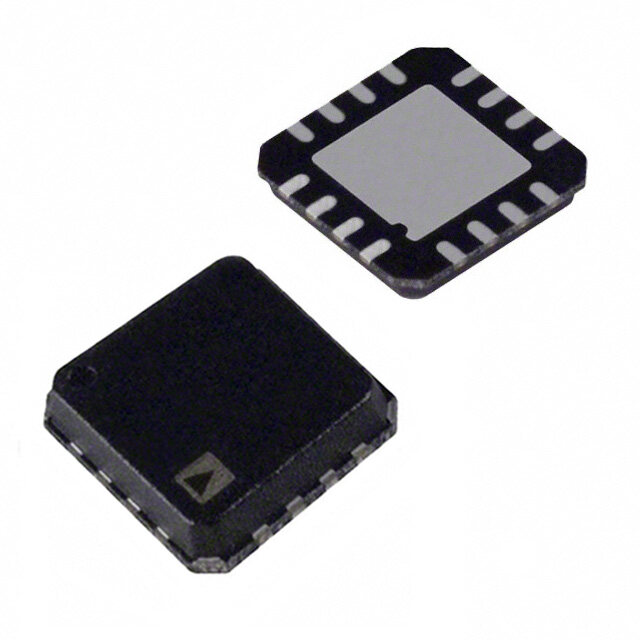
| 产品图片 |
|
| rohs | 符合RoHS无铅 / 符合限制有害物质指令(RoHS)规范要求 |
| 产品系列 | 放大器 IC,运算放大器 - 运放,Texas Instruments LMH6550MM/NOPB- |
| 数据手册 | |
| 产品型号 | LMH6550MM/NOPB |
| 产品目录页面 | |
| 产品种类 | 运算放大器 - 运放 |
| 供应商器件封装 | 8-VSSOP |
| 共模抑制比—最小值 | 72 dB |
| 关闭 | Shutdown |
| 其它名称 | LMH6550MM/NOPBDKR |
| 制造商产品页 | http://www.ti.com/general/docs/suppproductinfo.tsp?distId=10&orderablePartNumber=LMH6550MM/NOPB |
| 包装 | Digi-Reel® |
| 压摆率 | 3000 V/µs |
| 双重电源电压 | +/- 3 V, +/- 5 V |
| 商标 | Texas Instruments |
| 增益带宽积 | - |
| 安装类型 | 表面贴装 |
| 安装风格 | SMD/SMT |
| 封装 | Reel |
| 封装/外壳 | 8-TSSOP,8-MSOP(0.118",3.00mm 宽) |
| 封装/箱体 | VSSOP-8 |
| 工作温度 | -40°C ~ 85°C |
| 工作电源电压 | 5 V, 9 V |
| 工厂包装数量 | 1000 |
| 放大器类型 | 电压反馈 |
| 最大工作温度 | + 85 C |
| 最小双重电源电压 | +/- 2.25 V |
| 最小工作温度 | - 40 C |
| 标准包装 | 1 |
| 电压-电源,单/双 (±) | 4.5 V ~ 12 V, ±2.25 V ~ 6 V |
| 电压-输入失调 | 1mV |
| 电流-电源 | 20mA |
| 电流-输入偏置 | 8µA |
| 电流-输出/通道 | 75mA |
| 电源电流 | 20 mA |
| 电路数 | 1 |
| 系列 | LMH6550 |
| 设计资源 | http://www.digikey.com/product-highlights/cn/zh/texas-instruments-webench-design-center/3176 |
| 转换速度 | 3000 V/us |
| 输入偏压电流—最大 | 16 uA |
| 输入补偿电压 | 6 mV |
| 输出电流 | 75 mA |
| 输出类型 | 差分 |
| 通道数量 | 1 Channel |
| 配用 | /product-detail/zh/LMH730154%2FNOPB/LMH730154%2FNOPB-ND/723557 |


- 商务部:美国ITC正式对集成电路等产品启动337调查
- 曝三星4nm工艺存在良率问题 高通将骁龙8 Gen1或转产台积电
- 太阳诱电将投资9.5亿元在常州建新厂生产MLCC 预计2023年完工
- 英特尔发布欧洲新工厂建设计划 深化IDM 2.0 战略
- 台积电先进制程称霸业界 有大客户加持明年业绩稳了
- 达到5530亿美元!SIA预计今年全球半导体销售额将创下新高
- 英特尔拟将自动驾驶子公司Mobileye上市 估值或超500亿美元
- 三星加码芯片和SET,合并消费电子和移动部门,撤换高东真等 CEO
- 三星电子宣布重大人事变动 还合并消费电子和移动部门
- 海关总署:前11个月进口集成电路产品价值2.52万亿元 增长14.8%


PDF Datasheet 数据手册内容提取
Product Sample & Technical Tools & Support & Folder Buy Documents Software Community LMH6550 SNOSAK0I–DECEMBER2004–REVISEDJANUARY2015 LMH6550 Differential, High-Speed Operational Amplifier 1 Features 3 Description • 400MHz−3-dBBandwidth(V =0.5V ) The LMH6550 device is a high-performance voltage 1 OUT PP feedback differential amplifier. The LMH6550 has the • 90MHz0.1-dBBandwidth high speed and low distortion necessary for driving • 3000V/µsSlewRate high-performance ADCs as well as the current • 8nsSettlingTimeto0.1% handling capability to drive signals over balanced transmission lines like CAT 5 data cables. The • −92/−103dBHD2/HD3at5MHz LMH6550 can handle a wide range of video and data • 10nsShutdown/Enable formats. 2 Applications With external gain set resistors, the LMH6550 can be used at any desired gain. Gain flexibility coupled with • DifferentialADDriver high speed makes the LMH6550 suitable for use as • VideoOverTwisted-Pair an IF amplifier in high-performance communications equipment. • DifferentialLineDriver • SingleEndtoDifferentialConverter The LMH6550 is available in the space-saving SOIC andVSSOPpackages. • High-SpeedDifferentialSignaling • IF/RFAmplifier DeviceInformation(1) • SAWFilterBuffer/Driver PARTNUMBER PACKAGE BODYSIZE(NOM) SOIC(8) 4.90mm×3.91mm LMH6550 VSSOP(8) 3.00mm×3.00mm (1) For all available packages, see the orderable addendum at theendofthedatasheet. 4 Typical Application Schematic RF AV, RIN + V RS VI RG RO + - IN- VSa RT VCM VO ADC + IN+ - RG RO RM V- RF For R (cid:31)(cid:31) R : DesignTarget: M G V R A O # F 1) Set R 1 v V R T 1 (cid:16) 1 I G R R 2R (1(cid:14)A ) S IN R # G v IN 2(cid:14)A 2) Set R R ||R M T S v 1 An IMPORTANT NOTICE at the end of this data sheet addresses availability, warranty, changes, use in safety-critical applications, intellectualpropertymattersandotherimportantdisclaimers.PRODUCTIONDATA.
LMH6550 SNOSAK0I–DECEMBER2004–REVISEDJANUARY2015 www.ti.com Table of Contents 1 Features.................................................................. 1 8.4 DeviceFunctionalModes........................................13 2 Applications........................................................... 1 9 ApplicationandImplementation........................ 14 3 Description............................................................. 1 9.1 ApplicationInformation............................................14 4 TypicalApplicationSchematic............................. 1 9.2 TypicalApplications................................................14 5 RevisionHistory..................................................... 2 10 PowerSupplyRecommendations..................... 22 6 PinConfigurationandFunctions......................... 3 11 Layout................................................................... 22 11.1 LayoutGuidelines.................................................22 7 Specifications......................................................... 3 11.2 LayoutExample....................................................22 7.1 AbsoluteMaximumRatings......................................3 11.3 PowerDissipation.................................................24 7.2 ESDRatings..............................................................3 11.4 ESDProtection......................................................24 7.3 RecommendedOperatingConditions.......................4 12 DeviceandDocumentationSupport................. 25 7.4 ThermalInformation..................................................4 7.5 ElectricalCharacteristics:±5V.................................4 12.1 DeviceSupport......................................................25 7.6 ElectricalCharacteristics:5V...................................6 12.2 DocumentationSupport........................................25 7.7 TypicalCharacteristics..............................................8 12.3 Trademarks...........................................................25 12.4 ElectrostaticDischargeCaution............................25 8 DetailedDescription............................................ 12 12.5 Glossary................................................................25 8.1 Overview.................................................................12 13 Mechanical,Packaging,andOrderable 8.2 FunctionalBlockDiagram.......................................12 Information........................................................... 25 8.3 FeatureDescription.................................................12 5 Revision History NOTE:Pagenumbersforpreviousrevisionsmaydifferfrompagenumbersinthecurrentversion. ChangesfromRevisionH(March2013)toRevisionI Page • AddedESDRatingstable,FeatureDescriptionsection,DeviceFunctionalModes,ApplicationandImplementation section,PowerSupplyRecommendationssection,Layoutsection,DeviceandDocumentationSupportsection,and Mechanical,Packaging,andOrderableInformationsection.................................................................................................. 1 ChangesfromRevisionG(March2013)toRevisionH Page • ChangedlayoutofNationalDataSheettoTIformat........................................................................................................... 22 2 SubmitDocumentationFeedback Copyright©2004–2015,TexasInstrumentsIncorporated ProductFolderLinks:LMH6550
LMH6550 www.ti.com SNOSAK0I–DECEMBER2004–REVISEDJANUARY2015 6 Pin Configuration and Functions DPackage/DGKPackage 8Pins TopView 1 8 -IN +IN - + 2 7 VCM EN 3 6 V+ V- 4 5 +OUT -OUT PinFunctions PIN I/O DESCRIPTION NAME NO. EN 7 I Enable -IN 1 I NegativeInput +IN 8 I PositiveInput -OUT 5 O NegativeOutput +OUT 4 O PositiveOutput V- 6 P NegativeSupply V+ 3 P PositiveSupply VCM 2 I OutputCommon-ModeInput 7 Specifications 7.1 Absolute Maximum Ratings(1)(2)(3) MIN MAX UNIT SupplyVoltage 13.2 V Common-ModeInputVoltage ±V V S MaximumInputCurrent(pins1,2,7,8) 30 mA MaximumOutputCurrent(pins4,5) (4) MaximumJunctionTemperature 150 °C StorageTemperature,T −65 150 °C stg (1) StressesbeyondthoselistedunderAbsoluteMaximumRatingsmaycausepermanentdamagetothedevice.Thesearestressratings only,whichdonotimplyfunctionaloperationofthedeviceattheseoranyotherconditionsbeyondthoseindicatedunderRecommended OperatingConditions.Exposuretoabsolute-maximum-ratedconditionsforextendedperiodsmayaffectdevicereliability. (2) IfMilitary/Aerospacespecifieddevicesarerequired,pleasecontacttheTexasInstrumentsSalesOffice/Distributorsforavailabilityand specifications. (3) ForSolderingInformation,seeProductFolderatwww.ti.comandSNOA549. (4) Themaximumoutputcurrent(I )isdeterminedbydevicepowerdissipationlimitations. OUT 7.2 ESD Ratings VALUE UNIT Human-bodymodel(HBM),perANSI/ESDA/JEDECJS-001(2) ±2000 V Electrostaticdischarge(1) V (ESD) Machinemodel(MM) ±200 (1) Humanbodymodel:1.5kΩinserieswith100pF.Machinemodel:0Ωinserieswith200pF. (2) JEDECdocumentJEP155statesthat500-VHBMallowssafemanufacturingwithastandardESDcontrolprocess. Copyright©2004–2015,TexasInstrumentsIncorporated SubmitDocumentationFeedback 3 ProductFolderLinks:LMH6550
LMH6550 SNOSAK0I–DECEMBER2004–REVISEDJANUARY2015 www.ti.com 7.3 Recommended Operating Conditions MIN NOM MAX UNIT OperatingTemperature −40 85 °C TotalSupplyVoltage 4.5 12 V 7.4 Thermal Information LMH6550 THERMALMETRIC(1) D DGK UNIT 8PINS 8PINS R Junction-to-ambientthermalresistance (2) 150 235 °C/W θJA (1) Formoreinformationabouttraditionalandnewthermalmetrics,seetheICPackageThermalMetricsapplicationreport,SPRA953. (2) ThemaximumpowerdissipationisafunctionofT ,θ andT .Themaximumallowablepowerdissipationatanyambient J(MAX) JA A temperatureisP =(T —T )/θ .Allnumbersapplyforpackagesoldereddirectlyintoa2layerPCboardwithzeroairflow. D J(MAX) A JA 7.5 Electrical Characteristics: ±5 V(1) Single-endedindifferentialout,T =25°C,V =±5V,V =0V,R =R =365Ω,R =500Ω;unlessspecified. A S CM F G L PARAMETER TESTCONDITIONS MIN (2) TYP (3) MAX (2) UNIT ACPERFORMANCE(DIFFERENTIAL) SSBW SmallSignal−3dBBandwidth V =0.5V 400 MHz OUT PP LSBW LargeSignal−3dBBandwidth V =2V 380 MHz OUT PP LargeSignal−3dBBandwidth V =4V 320 MHz OUT PP 0.1dBBandwidth V =0.5V 90 MHz OUT PP SlewRate 4-VStep (4) 2000 3000 V/μs Rise/FallTime 2-VStep 1 ns SettlingTime 2-VStep,0.1% 8 ns V PINACPERFORMANCE(COMMON-MODEFEEDBACKAMPLIFIER) CM Common-ModeSmallSignal V BypassCapacitorRemoved 210 MHz CM Bandwidth SlewRate V BypassCapacitorRemoved 200 V/µs CM DISTORTIONANDNOISERESPONSE HD2 2ndHarmonicDistortion V =2V ,f=5MHz,R =800Ω −92 O PP L V =2V ,f=20MHz,R =800Ω −78 dBc O PP L V =2V ,f=70MHz,R =800Ω −59 O PP L HD3 3rdHarmonicDistortion V =2V ,f=5MHz,R =800Ω −103 O PP L V =2V ,f=20MHz,R =800Ω −88 dBc O PP L V =2V ,f=70MHz,R =800Ω −50 O PP L e InputReferredVoltageNoise f≥1MHz 6.0 nV/√Hz n i InputReferredNoiseCurrent f≥1MHz 1.5 pA/√Hz n INPUTCHARACTERISTICS(DIFFERENTIAL) V InputOffsetVoltage DifferentialMode,V = 1 ±4 mV OSD ID 0,V =0 CM Atextreme ±6 temperatures InputOffsetVoltageAverage (5) 1.6 µV/°C TemperatureDrift I InputBiasCurrent (6) 0 -8 −16 µA BI (1) ElectricalTablevaluesapplyonlyforfactorytestingconditionsatthetemperatureindicated.Factorytestingconditionsresultinvery limitedself-heatingofthedevicesuchthatT =T . J A (2) Limitsare100%productiontestedat25°C.Limitsovertheoperatingtemperaturerangeareguaranteedthroughcorrelationusing StatisticalQualityControl(SQC)methods. (3) Typicalnumbersarethemostlikelyparametricnorm. (4) SlewRateistheaverageoftherisingandfallingedges. (5) Driftdeterminedbydividingthechangeinparameterattemperatureextremesbythetotaltemperaturechange. (6) Negativeinputcurrentimpliescurrentflowingoutofthedevice. 4 SubmitDocumentationFeedback Copyright©2004–2015,TexasInstrumentsIncorporated ProductFolderLinks:LMH6550
LMH6550 www.ti.com SNOSAK0I–DECEMBER2004–REVISEDJANUARY2015 Electrical Characteristics: ±5 V(1) (continued) Single-endedindifferentialout,T =25°C,V =±5V,V =0V,R =R =365Ω,R =500Ω;unlessspecified. A S CM F G L PARAMETER TESTCONDITIONS MIN (2) TYP (3) MAX (2) UNIT InputBiasCurrentAverage (5) 9.6 nA/°C TemperatureDrift InputBiasDifference DifferenceinBiasCurrentsBetweenthe 0.3 µA TwoInputs CMRR Common-ModeRejectionRatio DC,V =0V,V =0V 72 82 dBc CM ID R InputResistance Differential 5 MΩ IN C InputCapacitance Differential 1 pF IN CMVR InputCommon-ModeVoltageRange CMRR>53dB +3.1 +3.2 V −4.6 −4.7 V PININPUTCHARACTERISTICS(COMMON-MODEFEEDBACKAMPLIFIER) CM V InputOffsetVoltage CommonMode,V =0 1 ±5 mV OSC ID Atextreme ±8 temperatures InputOffsetVoltageAverage (5) 25 µV/°C TemperatureDrift InputBiasCurrent (6) −2 μA V CMRR V =0V,1-VSteponV Pin,Measure 70 75 dB CM ID CM V OD InputResistance 25 kΩ Common-ModeGain ΔV /ΔV 0.995 0.997 1.005 V/V O,CM CM OUTPUTPERFORMANCE OutputVoltageSwing PeaktoPeak, 7.38 7.8 V Differential Atextreme 7.18 temperatures OutputCommon-ModeVoltage V =0V, ±3.69 ±3.8 V ID Range I LinearOutputCurrent V =0V ±63 ±75 mA OUT OUT I ShortCircuitCurrent OutputShortedtoGround ±200 mA SC V =3VSingle-Ended (7) IN OutputBalanceError ΔV CommonMode/ΔV −68 dB OUT OUT Differential,V =1V Differential,f= OUT PP 10MHz MISCELLANEOUSPERFORMANCE EnableVoltageThreshold Pin7 2.0 V DisableVoltageThreshold Pin7 1.5 V EnablePinCurrent V =0V (6) -250 µA EN V =4V (6) 55 EN Enable/DisableTime 10 ns A OpenLoopGain Differential 70 dB VOL PSRR PowerSupplyRejectionRatio DC,ΔV =±1V 74 90 dB S SupplyCurrent R =∞ 18 20 24 mA L Atextreme 27 temperatures DisabledSupplyCurrent 1 1.2 mA (7) Themaximumoutputcurrent(I )isdeterminedbydevicepowerdissipationlimitations. OUT Copyright©2004–2015,TexasInstrumentsIncorporated SubmitDocumentationFeedback 5 ProductFolderLinks:LMH6550
LMH6550 SNOSAK0I–DECEMBER2004–REVISEDJANUARY2015 www.ti.com 7.6 Electrical Characteristics: 5 V(1) Single-endedindifferentialout,T =25°C,A =+1,V =5V,V =2.5V,R =R =365Ω,R =500Ω;unlessspecified. A V S CM F G L PARAMETER TESTCONDITIONS MIN (2) TYP (3) MAX (2) UNIT SSBW SmallSignal−3dBBandwidth R =500Ω,V =0.5V 350 MHz L OUT PP LSBW LargeSignal−3dBBandwidth R =500Ω,V =2V 330 MHz L OUT PP 0.1dBBandwidth 60 MHz SlewRate 2-VStep (4) 1500 V/μs Rise/FallTime,10%to90% 1-VStep 1 ns SettlingTime 1-VStep,0.05% 12 ns V PINACPERFORMANCE(COMMON-MODEFEEDBACKAMPLIFIER) CM Common-ModeSmallSignal 185 MHz Bandwidth SlewRate 180 V/μs DISTORTIONANDNOISERESPONSE HD2 2ndHarmonicDistortion V =2V ,f=5MHz,R =800Ω −89 O PP L dBc V =2V ,f=20MHz,R =800Ω −88 O PP L HD3 3rdHarmonicDistortion V =2V ,f=5MHz,R =800Ω −85 O PP L dBc V =2V ,f=20MHz,R =800Ω −70 O PP L e InputReferredNoiseVoltage f≥1MHz 6.0 nV/√Hz n i InputReferredNoiseCurrent f≥1MHz 1.5 pA/√Hz n INPUTCHARACTERISTICS(DIFFERENTIAL) V InputOffsetVoltage DifferentialMode,V = 1 ±4 mV OSD ID 0,V =0 CM Atextreme ±6 temperatures InputOffsetVoltageAverage (5) 1.6 µV/°C TemperatureDrift I InputBiasCurrent (6) 0 −8 −16 μA BIAS InputBiasCurrentAverage (5) 9.5 nA/°C TemperatureDrift InputBiasCurrentDifference DifferenceinBiasCurrentsBetweenthe 0.3 µA TwoInputs CMRR Common-ModeRejectionRatio DC,V =0V 70 80 dBc ID InputResistance Differential 5 MΩ InputCapacitance Differential 1 pF V InputCommon-ModeRange CMRR>53dB +3.1 +3.2 ICM +0.4 +0.3 V PININPUTCHARACTERISTICS(COMMON-MODEFEEDBACKAMPLIFIER) CM InputOffsetVoltage Common-Mode,V =0 1 ±5 mV ID Atextreme ±8 temperatures InputOffsetVoltageAverage 18.6 µV/°C TemperatureDrift InputBiasCurrent 3 μA V CMRR V =0, 70 75 dB CM ID 1-VSteponV Pin,MeasureV CM OD InputResistance V PintoGround 25 kΩ CM (1) ElectricalTablevaluesapplyonlyforfactorytestingconditionsatthetemperatureindicated.Factorytestingconditionsresultinvery limitedself-heatingofthedevicesuchthatT =T . J A (2) Limitsare100%productiontestedat25°C.Limitsovertheoperatingtemperaturerangeareguaranteedthroughcorrelationusing StatisticalQualityControl(SQC)methods. (3) Typicalnumbersarethemostlikelyparametricnorm. (4) SlewRateistheaverageoftherisingandfallingedges. (5) Driftdeterminedbydividingthechangeinparameterattemperatureextremesbythetotaltemperaturechange. (6) Negativeinputcurrentimpliescurrentflowingoutofthedevice. 6 SubmitDocumentationFeedback Copyright©2004–2015,TexasInstrumentsIncorporated ProductFolderLinks:LMH6550
LMH6550 www.ti.com SNOSAK0I–DECEMBER2004–REVISEDJANUARY2015 Electrical Characteristics: 5 V(1) (continued) Single-endedindifferentialout,T =25°C,A =+1,V =5V,V =2.5V,R =R =365Ω,R =500Ω;unlessspecified. A V S CM F G L PARAMETER TESTCONDITIONS MIN (2) TYP (3) MAX (2) UNIT Common-ModeGain ΔV /ΔV 0.991 V/V O,CM CM OUTPUTPERFORMANCE V OutputVoltageSwing PeaktoPeak,Differential, 2.4 2.8 V OUT V =±2.5V,V =0V S CM I LinearOutputCurrent V =0-VDifferential ±54 ±70 mA OUT OUT I OutputShortCircuitCurrent OutputShortedtoGround 250 mA SC V =3VSingle-Ended (7) IN CMVR Common-ModeVoltageRange V =0,V Pin=1.2Vand3.8V 3.72 3.8 ID CM V 1.23 1.2 OutputBalanceError ΔV CommonMode/ΔV −65 dB OUT OUT DIfferential,V =1V Differential,f= OUT PP 10MHz MISCELLANEOUSPERFORMANCE EnableVoltageThreshold Pin7 2.0 V DisableVoltageThreshold Pin7 1.5 V EnablePinCurrent V =0V (6) -250 µA EN V =4V (6) 55 EN Enable/DisableTime 10 ns OpenLoopGain DC,Differential 70 dB PSRR PowerSupplyRejectionRatio DC,ΔV =±0.5V 72 77 dB S I SupplyCurrent R =∞ 16.5 19 23.5 mA S L Atextreme 26.5 temperatures I DisabledSupplyCurrent 1 1.2 mA SD (7) Themaximumoutputcurrent(I )isdeterminedbydevicepowerdissipationlimitations. OUT Copyright©2004–2015,TexasInstrumentsIncorporated SubmitDocumentationFeedback 7 ProductFolderLinks:LMH6550
LMH6550 SNOSAK0I–DECEMBER2004–REVISEDJANUARY2015 www.ti.com 7.7 Typical Characteristics (T =25°C,V =±5V,R =500Ω,R =R =365Ω;unlessspecified). A S L F G 1 1 0 0 -1 VS = 5V -1 VS = 5V -2 -2 VS = ±5V VS = ±5V )B -3 )B -3 d d ( N -4 ( N -4 IA IA G -5 G -5 -6 -6 -7 VOD = 0.5VPP -7 VOD = 1VPP AV = 1 AV = 1 -8 -8 DIFFERENTIAL INPUT SINGLE ENDED INPUT -9 -9 1 10 100 1000 1 10 100 1000 FREQUENCY (MHz) FREQUENCY (MHz) Figure1.FrequencyResponsevsSupplyVoltage Figure2.FrequencyResponse 1 1 0 0 GAIN = 2 --21 VOD = 4.0VPP )Bd( N --21 )Bd( N --43 VOD = 0.5VPP IAG DE --43 GAIN = 4 IAG -5 VOD = 2.0VPP ZILAM -5 GAIN = 6 -6 R -6 O -7 Vs = ±5V N -7 -8 AV = 1 -8 VOUT = 0.5 VPP SINGLE ENDED INPUT SINGLE ENDED INPUT -9 -9 1 10 100 1000 1 10 100 1000 FREQUENCY (MHz) FREQUENCY (MHz) Figure4.FrequencyResponsevsGain Figure3.FrequencyResponsevsV OUT 2 70 CL = 5.7 pF, ROUT = 40: VS = ±5V 1 60 0 -1 CL = 10 pF, ROUT = 30: :) 50 )Bd( NIAG ---432 CCLL == 2427 ppFF,, RROOUUTT == 2123:: ( R DETSEO 3400 G -5 VOD = 210 mVPP GUS 20 -6 AV = 1 LOAD = 1 k: || CAP LOAD -7 LSOEARDIE =S (WCILT |H| 12 kR:O) UINT S 10 VS = ±5V -8 0 1 10 100 1000 1 10 100 FREQUENCY (MHz) CAPACITIVE LOAD (pF) Figure5.FrequencyResponsevsCapacitiveLoad Figure6.SuggestedR vsCapLoad OUT 8 SubmitDocumentationFeedback Copyright©2004–2015,TexasInstrumentsIncorporated ProductFolderLinks:LMH6550
LMH6550 www.ti.com SNOSAK0I–DECEMBER2004–REVISEDJANUARY2015 Typical Characteristics (continued) (T =25°C,V =±5V,R =500Ω,R =R =365Ω;unlessspecified). A S L F G 1.5 2.5 2 1 1.5 1 0.5 )V )V 0.5 ( T 0 ( T 0 U U O O V V -0.5 -0.5 -1 RL = 500: VS = ±5 -1.5 RF = 360: -1 RL = 500: SINGLE ENDED RF = 360: -2 INPUT -1.5 -2.5 0 10 20 30 40 50 60 70 80 90 100 0 10 20 30 40 50 60 70 80 90 100 TIME (ns) TIME (ns) Figure7.2V PulseResponseSingle-EndedInput Figure8.LargeSignalPulseResponse PP 40 -30 30 -40 )V 20 HD3 m ( V ETUO 100 )cBd( NO --5600 DOM N --2100 ITROT -70 OM -30 SID -80 VS = 5V MO -40 RL = 500: HD2 RL = 800: C RF = 360: -90 VOD = 2 VPP -50 VOD = 4 VPP VOCM = 2.5V -60 -100 0 10 20 30 40 50 60 70 80 90 100 0 10 20 30 40 50 60 70 TIME (ns) FREQUENCY (MHz) Figure9.OutputCommon-ModePulseResponse Figure10.DistortionvsFrequencySingle-EndedInput -40 4 3.9 -50 HD3 3.8 )cB -60 )V 3.7 d( N -70 ( TU 3.6 O O ITROT -80 V MUM 33..45 SID -90 HD2 VS = ±5V IXA 3.3 VS = ±5V RL = 800: M AV = 2 3.2 -100 VOD = 2 VPP RF = 730: VOCM = 0V 3.1 VIN = 3.88V SINGLE ENDED -110 3 0 10 20 30 40 50 60 70 0 -10 -20 -30 -40 -50-60 -70 -80 -90-100 FREQUENCY (MHz) OUTPUT CURRENT (mA) Figure11.DistortionvsFrequencySingle-EndedInput Figure12.MaximumV vsI OUT OUT Copyright©2004–2015,TexasInstrumentsIncorporated SubmitDocumentationFeedback 9 ProductFolderLinks:LMH6550
LMH6550 SNOSAK0I–DECEMBER2004–REVISEDJANUARY2015 www.ti.com Typical Characteristics (continued) (T =25°C,V =±5V,R =500Ω,R =R =365Ω;unlessspecified). A S L F G -3 100 VS = ±5V VS = ±5V -3.1 AV = 2 VIN = 0V -3.2 RF = 730: 10 AV = 1 )V -3.3 VIN = 3.88V SINGLE ENDED ( TU -3.4 V MUMO --33..65 :)( |Z| 1 IN IM -3.7 0.1 -3.8 -3.9 -4 0.01 0 10 20 30 40 50 60 70 80 90 100 0.01 0.1 1 10 100 1000 OUTPUT CURRENT (mA) FREQUENCY (MHz) Figure13.MinimumV vsI Figure14.Closed-LoopOutputImpedance OUT OUT 100 100 VS = 5V 90 VIN = 0V PSRR - 10 AV = 1 )LAITN 8700 E PSRR + RE 60 :)( |Z| 1 FFID cB 4500 d ( R 30 VS = ±5V 0.1 RSP 20 RL = 500: AV = 1 10 VIN = 0V 0.01 0 0.01 0.1 1 10 100 1000 0.01 0.1 1 10 100 1000 FREQUENCY (MHz) FREQUENCY (MHz) Figure15.Closed-LoopOutputImpedance Figure16.PSRR 100 85 90 80 PSRR - )LA 80 75 ITNEREF 6700 PSRR + )Bd( R 6750 FID 50 RM 60 cB 40 C d( R 30 VS = 5V 55 RS 20 RL = 500: 50 P 10 AV = 1 45 VIN = 2.5V 0 40 0.01 0.1 1 10 100 1000 0.1 1 10 100 1000 FREQUENCY (MHz) FREQUENCY (MHz) Figure17.PSRR Figure18.CMRR 10 SubmitDocumentationFeedback Copyright©2004–2015,TexasInstrumentsIncorporated ProductFolderLinks:LMH6550
LMH6550 www.ti.com SNOSAK0I–DECEMBER2004–REVISEDJANUARY2015 Typical Characteristics (continued) (T =25°C,V =±5V,R =500Ω,R =R =365Ω;unlessspecified). A S L F G -25 -40 )cB ---433005 RRAVLF === 5310600:: VS = 5V --5405 VARSVL === 2±205 V0V/:V f = 40 MHz d( RORRE E ----65540505 VS = ±5V MD 3 (dBc) ---665505 f = 20 MHz CN -65 I -70 A -70 f = 5 MHz L AB -75 -75 -80 -80 -85 -85 -90 0 1 2 3 4 5 6 7 1 10 100 1000 FREQUENCY (MHz) DIFFERENTIAL VOUT (VPP) Figure19.BalanceError Figure20.Third-OrderIntermodulationProductsvsV OUT Copyright©2004–2015,TexasInstrumentsIncorporated SubmitDocumentationFeedback 11 ProductFolderLinks:LMH6550
LMH6550 SNOSAK0I–DECEMBER2004–REVISEDJANUARY2015 www.ti.com 8 Detailed Description 8.1 Overview The LMH6550 is a fully differential amplifier designed to provide low distortion amplification to wide bandwidth differential signals. The LMH6550, though fully integrated for ultimate balance and distortion performance, functionally provides three channels. Two of these channels are the V+ and V− signal path channels, which function similarly to inverting mode operational amplifiers and are the primary signal paths. The third channel is the common-mode feedback circuit. This is the circuit that sets the output common mode as well as driving the V+ and V− outputs to be equal magnitude and opposite phase, even when only one of the two input channels is driven.Thecommon-modefeedbackcircuitallowssingle-endedtodifferentialoperation. 8.2 Functional Block Diagram V+ +OUT -IN ± 2.5 k(cid:13) High-Aol + Differential I/O Amplifier ± 2.5 k(cid:13) +IN + -OUT V+ 50 k(cid:13) ± Vcm Error Amplifier + Vcm EN Buffer 50 k(cid:13) V± 8.3 Feature Description The LMH6550 combines a core differential I/O, high-gain block with an output common-mode sense that is compared to a reference voltage and then fed back into the main amplifier block to control the average output to that reference. The differential I/O block is a classic, high open-loop gain stage. The high-speed differential outputs include an internal averaging resistor network to sense the output common-mode voltage. This voltage is compared by a separate Vcm error amplifier to the voltage on the Vocm pin. If floated, this reference is at half the total supply voltage across the device using two 50-kΩ resistors. This Vcm error amplifier transmits a correction signal into the main amplifier to force the output average voltage to meet the target voltage on the Vocmpin. 12 SubmitDocumentationFeedback Copyright©2004–2015,TexasInstrumentsIncorporated ProductFolderLinks:LMH6550
LMH6550 www.ti.com SNOSAK0I–DECEMBER2004–REVISEDJANUARY2015 8.4 Device Functional Modes This wideband FDA requires external resistors for correct signal-path operation. When configured for the desired input impedance and gain setting with these external resistors, the amplifier can be either on with the PD pin asserted to a voltage greater than Vs– + 1.7 V, or turned off by asserting PD low. Disabling the amplifier shuts off the quiescent current and stops correct amplifier operation. The signal path is still present for the source signal through the external resistors. The Vocm control pin sets the output average voltage. Left open, Vocm defaults to an internal midsupply value. Driving this high-impedance input with a voltage reference within its valid rangesetsatargetfortheinternalVcmerroramplifier. Copyright©2004–2015,TexasInstrumentsIncorporated SubmitDocumentationFeedback 13 ProductFolderLinks:LMH6550
LMH6550 SNOSAK0I–DECEMBER2004–REVISEDJANUARY2015 www.ti.com 9 Application and Implementation NOTE Information in the following applications sections is not part of the TI component specification, and TI does not warrant its accuracy or completeness. TI’s customers are responsible for determining suitability of components for their purposes. Customers should validateandtesttheirdesignimplementationtoconfirmsystemfunctionality. 9.1 Application Information The LMH6550 is a fully differential amplifier designed to provide low distortion amplification to wide bandwidth differential signals. The LMH6550, though fully integrated for ultimate balance and distortion performance, functionally provides three channels. Two of these channels are the V+ and V− signal path channels, which function similarly to inverting mode operational amplifiers and are the primary signal paths. The third channel is the common-mode feedback circuit. This is the circuit that sets the output common mode as well as driving the V+ and V− outputs to be equal magnitude and opposite phase, even when only one of the two input channels is driven.Thecommon-modefeedbackcircuitallowssingle-endedtodifferentialoperation. The LMH6550 is a voltage feedback amplifier with gain set by external resistors. Output common-mode voltage issetbytheV pin.Thispinshouldbedrivenbyalowimpedancereferenceandshouldbebypassedtoground CM with a 0.1-µF ceramic capacitor. Any signal coupling into the V will be passed along to the output and will CM reducethedynamicrangeoftheamplifier. The LMH6550 is equipped with a ENABLE pin to reduce power consumption when not in use. The ENABLE pin floats to logic high. If this pin is not used it can be left floating. The amplifier output stage goes into a high impedance state when the amplifier is disabled. The feedback and gain set resistors will then set the impedance ofthecircuit.Forthisreasoninputtooutputisolationwillbepoorinthedisabledstate. 9.2 Typical Applications 9.2.1 TypicalFullyDifferentialApplication The LMH6550 performs best when used with split supplies and in a fully differential configuration. See Figure 21 andFigure22forrecommendcircuits. RF1 RO RG1 + VI a VCM CL RL VO - RG2 RO RF2 ENABLE Figure21. TypicalFullyDifferentialApplicationSchematic 9.2.1.1 DesignRequirements Applicationsusingfullydifferentialamplifiershaveseveralrequirements.Themainrequirementsarehighlinearity and good signal amplitude. Linearity is accomplished by using well matched feedback and gain set resistors as well as an appropriate supply voltage. The signal amplitude can be tailored by using an appropriate gain. In this design the gain is set for a gain of 2 (R =500/ R =250) and the distortion criteria is better than -90 dBc at a F G frequency of 5 Mhz. The supply voltages are set to +5 V and -5 V and the output common mode is 0 V. The LMH6550canbeplacedintoshutdowntoreducepowerdissipationto10mW. 14 SubmitDocumentationFeedback Copyright©2004–2015,TexasInstrumentsIncorporated ProductFolderLinks:LMH6550
LMH6550 www.ti.com SNOSAK0I–DECEMBER2004–REVISEDJANUARY2015 Typical Applications (continued) 9.2.1.2 DetailedDesignProcedure The power supplies for this design are symmetrical ±5-V supplies (not shown for simplicity). The ADC input common mode is 1 V which is within the optimum operating range for the LMH6550 when used on ±5-V split supplies. The gain of this circuit is equal to RF/RG and due to the split supplies can be set to gains of 15 V/V or less.HighergainswillresultinvaluesofRFthataretoolargeforhighspeedoperation. 9.2.1.2.1 FullyDifferentialOperation The circuit shown in is a typical fully differential application as might be used to drive an ADC. In this circuit closed loop gain, (A ) = V / V = R /R . For all the applications in this data sheet V is presumed to be the V OUT IN F G IN voltage presented to the circuit by the signal source. For differential signals this will be the difference of the signals on each input (which will be double the magnitude of each individual signal), while in single-ended inputs itwilljustbethedriveninputsignal. The resistors R help keep the amplifier stable when presented with a load C as is typical in an analog to digital O L converter (ADC). When fed with a differential signal, the LMH6550 provides excellent distortion, balance and common-mode rejection provided the resistors R , R and R are well matched and strict symmetry is observed F G O in board layout. With a DC CMRR of over 80 dB, the DC and low frequency CMRR of most circuits will be dominated by the external resistors and board trace resistance. At higher frequencies board layout symmetry becomes a factor as well. Precision resistors of at least 0.1% accuracy are recommended and careful board layoutwillalsoberequired. 500 50: 100: TWISTED PAIR 250 + a 2 VPP VCM - 250 2 VPP 50: 500 GAIN = 2 ENABLE Figure22. FullyDifferentialCableDriver With up to 15 V differential output voltage swing and 80 mA of linear drive current the LMH6550 makes an PP excellent cable driver as shown in Figure 22. The LMH6550 is also suitable for driving differential cables from a single-endedsource. The LMH6550 requires supply bypassing capacitors as shown in Figure 23 and Figure 24. The 0.01 µF and 0.1 µF capacitors should be leadless SMT ceramic capacitors and should be no more than 3 mm from the supply pins. The SMT capacitors should be connected directly to a ground plane. Thin traces or small vias will reduce the effectiveness of bypass capacitors. Also shown in both figures is a capacitor from the V pin to ground. The CM V pin is a high impedance input to a buffer which sets the output common-mode voltage. Any noise on this CM input is transferred directly to the output. Output common-mode noise will result in loss of dynamic range, degradedCMRR,degradedBalanceandhigherdistortion.TheV pinshouldbebypassedevenifthepininnot CM used. There is an internal resistive divider on chip to set the output common-mode voltage to the mid point of the supply pins. The impedance looking into this pin is approximately 25 kΩ. If a different output common-mode voltageisdesireddrivethispinwithaclean,accuratevoltagereference. Copyright©2004–2015,TexasInstrumentsIncorporated SubmitDocumentationFeedback 15 ProductFolderLinks:LMH6550
LMH6550 SNOSAK0I–DECEMBER2004–REVISEDJANUARY2015 www.ti.com Typical Applications (continued) V+ V+ 0.01 PF 0.01 PF 10 PF 0.01 PF 10 PF + + VCM 0.1 PF - VCM 0.1 PF - 0.1 PF 10 PF 0.01 PF - V Figure23.SplitSupplyBypassingCapacitors Figure24.SingleSupplyBypassingCapacitors 9.2.1.2.2 CapacitiveDrive As noted in Driving Analog-to-Digital Converters, capacitive loads should be isolated from the amplifier output withsmallvaluedresistors.Thisisparticularlythecasewhentheloadhasaresistivecomponentthatis500 Ωor higher. A typical ADC has capacitive components of around 10 pF and the resistive component could be 1000 Ω or higher. If driving a transmission line, such as 50-Ω coaxial or 100-Ω twisted pair, using matching resistors will be sufficient to isolate any subsequent capacitance. For other applications see Figure 6 and Figure 25 in Typical Characteristics. 9.2.1.2.3 ApplicationCurves Many application circuits have capacitive loading. As shown in Figure 25, amplifier bandwidth is reduced with increasingcapacitiveload,soparasiticcapacitanceshouldbestrictlylimited. To ensure stability, resistance should be added between the capacitive load and the amplifier output pins. The value of the resistor is dependent on the amount of capacitive load as shown in Figure 26. This resistive value is a suggestion. System testing will be required to determine the optimal value. Using a smaller resistor will retain more system bandwidth at the expense of overshoot and ringing, while larger values of resistance will reduce overshootbutwillalsoreducesystembandwidth. 70 0.8 60 0.6 0.4 :) 50 ( O 0.2 R DE 40 )V( T 0 T U SE 30 VO G -0.2 G U 20 S -0.4 VS = 5V 10 LOAD = 1 k: || CAP LOAD -0.6 RL = 500: VS = 5V RF = 360: 0 -0.8 1 10 100 0 10 20 30 40 50 60 70 80 90 100 CAPACITIVE LOAD (pF) TIME (ns) Figure25.SuggestedR vsCapLoad Figure26.1V PulseResponseSingle-EndedInput OUT PP 16 SubmitDocumentationFeedback Copyright©2004–2015,TexasInstrumentsIncorporated ProductFolderLinks:LMH6550
LMH6550 www.ti.com SNOSAK0I–DECEMBER2004–REVISEDJANUARY2015 Typical Applications (continued) 9.2.2 DrivingAnalog-to-DigitalConverters Analog-to-digital converters (ADC) present challenging load conditions. They typically have high-impedance inputs with large and often variable capacitive components. As well, there are usually current spikes associated with switched capacitor or sample and hold circuits. Figure 27 shows a typical circuit for driving an ADC. The two 56-Ω resistors serve to isolate the capacitive loading of the ADC from the amplifier and ensure stability. In addition, the resistors form part of a low pass filter which helps to provide anti alias and noise reduction functions. The two 39-pF capacitors help to smooth the current spikes associated with the internal switching circuits of the ADC and also are a key component in the low pass filtering of the ADC input. In the circuit of Figure 27 the cutoff frequency of the filter is 1/ (2*π*56 Ω *(39 pF + 14 pF)) = 53 MHz (which is slightly less than the sampling frequency). Note that the ADC input capacitance must be factored into the frequency response of the input filter, and that being a differential input the effective input capacitance is double. Also as shown in Figure 27 the input capacitance to many ADCs is variable based on the clock cycle. See the data sheet for your particularADCfordetails. The amplifier and ADC should be located as closely together as possible. Both devices require that the filter components be in close proximity to them. The amplifier needs to have minimal parasitic loading on the output traces and the ADC is sensitive to high frequency noise that may couple in on its input lines. Some high performance ADCs have an input stage that has a bandwidth of several times its sample rate. The sampling process results in all input signals presented to the input stage mixing down into the Nyquist range (DC to Fs/2). See AN-236 for more details on the subsampling process and the requirements this imposes on the filtering necessaryinyoursystem. RF1 56 ADC12LO66 RG1 39 pF + a VI VCM - 7 - 8 pF 39 pF RG2 56 VREF RF2 ENABLE 1V LOW IMPEDANCE VOLTAGE REFERENCE Figure27. DrivinganADC Copyright©2004–2015,TexasInstrumentsIncorporated SubmitDocumentationFeedback 17 ProductFolderLinks:LMH6550
LMH6550 SNOSAK0I–DECEMBER2004–REVISEDJANUARY2015 www.ti.com Typical Applications (continued) 9.2.3 Single-EndedInputtoDifferentialOutput The LMH6550 provides excellent performance as an active balun transformer. Figure 28 shows a typical applicationwhereanLMH6550isusedtoproduceadifferentialsignalfromasingle-endedsource. In single-ended input operation the output common-mode voltage is set by the V pin as in fully differential CM mode. Also, in this mode the common-mode feedback circuit must recreate the signal that is not present on the unused differential input pin. Figure 19 is the measurement of the effectiveness of this process. The common- mode feedback circuit is responsible for ensuring balanced output with a single-ended input. Balance error is defined as the amount of input signal that couples into the output common mode. It is measured as a the undesired output common-mode swing divided by the signal on the input. Balance error can be caused by either a channel to channel gain error, or phase error. Either condition will produce a common-mode shift. Figure 19 measures the balance error with a single-ended input as that is the most demanding mode of operation for the amplifier. Supply and V pin bypassing are also critical in this mode of operation. See the above section on for bypassing CM recommendationsandalsoseeFigure23andFigure24forrecommendedsupplybypassingconfigurations. RF AV, RIN + V RS VI RG VI1 VO1 RO + - IN- VSa RT VCM VO ADC + IN+ - RG VI2 VO2 RO RM + V- - RF Conditions: Definitions: R R R ||R (cid:21) G S T IN 1 R (cid:14)R R R ||R G F M T S (cid:21) RG(cid:14)RM 2 R (cid:14)R (cid:14)R G M F V 2(1(cid:16)(cid:21) ) R A O 1 # F for R (cid:31)(cid:31) R v V (cid:21) (cid:14)(cid:21) R M G I 1 2 G (cid:21) R (1(cid:14) 2) 2R (cid:14)R (1(cid:16)(cid:21) ) G (cid:21) 2R (1(cid:14)A ) R G M 2 1 # G v for R (cid:31)(cid:31) R IN 1(cid:14)(cid:21) 1(cid:14)(cid:21) 2(cid:14)A M G 2 2 v V (cid:14)V V V O1 O2 (by design) OCM CM 2 V (cid:14)V V V I1 I2 V .(cid:21) # OCM for R (cid:31)(cid:31) R ICM 2 OCM 2 1(cid:14)A M G v Figure28. Single-EndedInputtoDifferentialOutputSchematic 18 SubmitDocumentationFeedback Copyright©2004–2015,TexasInstrumentsIncorporated ProductFolderLinks:LMH6550
LMH6550 www.ti.com SNOSAK0I–DECEMBER2004–REVISEDJANUARY2015 Typical Applications (continued) 9.2.4 SingleSupplyOperation The input stage of the LMH6550 has a built in offset of 0.7 V towards the lower supply to accommodate single supply operation with single-ended inputs. As shown in Figure 28, the input common-mode voltage is less than the output common voltage. It is set by current flowing through the feedback network from the device output. The input common-mode range of 0.4 V to 3.2 V places constraints on gain settings. Possible solutions to this limitation include AC coupling the input signal, using split power supplies and limiting stage gain. AC coupling withsinglesupplyisshowninFigure29. In Figure 28 closed loop gain = V / V ≊ R / R , where V =V / 2, as long as R << R . Note that in single- O I F G I S M G ended to differential operation V is measured single-ended while V is measured differentially. This means that I O gain is really 1/2 or 6 dB less when measured on either of the output pins separately. Additionally, note that the inputsignalatR (labeledasV)is1/2ofV whenR ischosentomatchR toR . T I S T S IN V =Inputcommon-modevoltage=(V +V )/2. ICM I1 I2 RF RO VO1 RS RG VI1 + VI a RT VCM CL RL VO - RG VI2 RM VO2 RO RF ENABLE VO1 + VO2 VICM = VOCM *V = CM 2 V1 + V2 I I *BY DESIGN VICM = 2 Figure29. AC-CoupledforSingleSupplyOperation Copyright©2004–2015,TexasInstrumentsIncorporated SubmitDocumentationFeedback 19 ProductFolderLinks:LMH6550
LMH6550 SNOSAK0I–DECEMBER2004–REVISEDJANUARY2015 www.ti.com Typical Applications (continued) 9.2.5 UsingTransformers Transformers are useful for impedance transformation as well as for single to differential, and differential to single-ended conversion. A transformer can be used to step up the output voltage of the amplifier to drive very high impedance loads as shown in Figure 30. Figure 32 shows the opposite case where the output voltage is steppeddowntodrivealow-impedanceload. Transformers have limitations that must be considered before choosing to use one. Compared to a differential amplifier, the most serious limitations of a transformer are the inability to pass DC and balance error (which causesdistortionandgainerrors).FormostapplicationstheLMH6550willhaveadequateoutputswinganddrive current and a transformer will not be desirable. Transformers are used primarily to interface differential circuits to 50-Ω single-endedtestequipmenttosimplifydiagnostictesting. 300: TWISTED PAIR 500 37.5: 1:2 (TURNS) 250 + a 4 VPP VCM - VCM 250 8 VPP 37.5: RL = 300: 500 AV = 2 ENABLE Figure30. TransformerOutHigh-ImpedanceLoad V * A * N IN V V = L § 2 R * N2 © ¨ OUT + 1¨ ¨ ¨ © RL § WHERE V = DIFFERENTIAL INPUT VOLTAGE IN § SECONDARY © N = TRANSFORMER TURNS RATIO = ¨ ¨ ¨ PRIMARY ¨ © § A = CLOSED LOOP AMPLIFIER GAIN V R = SERIES OUTPUT MATCHING RESISTOR OUT R = LOAD RESISTOR L V = VOLTAGE ACROSS LOAD RESISTOR L Figure31. CalculatingTransformerCircuitNetGain 20 SubmitDocumentationFeedback Copyright©2004–2015,TexasInstrumentsIncorporated ProductFolderLinks:LMH6550
LMH6550 www.ti.com SNOSAK0I–DECEMBER2004–REVISEDJANUARY2015 Typical Applications (continued) 100: TWISTED PAIR 375 200: 2:1 (TURNS) 375 + a 4 VPP VCM - VCM 375 1 VPP 200: RL = 100: 375 AV = 1 ENABLE Figure32. TransformerOutLow-ImpedanceLoad 50: COAX 375 100: 2:1 (TURNS) 375 + a 4 VPP VCM - C1 375 1 VPP 100: 375 ENABLE GAIN = 1 C1 IS NOT REQUIRED IF VCM = GROUND Figure33. Driving50-ΩTestEquipment Copyright©2004–2015,TexasInstrumentsIncorporated SubmitDocumentationFeedback 21 ProductFolderLinks:LMH6550
LMH6550 SNOSAK0I–DECEMBER2004–REVISEDJANUARY2015 www.ti.com 10 Power Supply Recommendations The LMH6550 can be used with any combination of positive and negative power supplies as long as the combined supply voltage is between 4.5 V and 12 V. The LMH6550 will provide best performance when the output voltage is set at the mid supply voltage, and when the total supply voltage is between 9 V and 12 V. When selecting a supply voltage that is less than 9 V it is important to consider both the input common-mode voltagerangeaswellastheoutputvoltagerange. Power supply bypassing as shown in Figure 23 and Figure 24 is important and power supply regulation should bewithin5%orbetterwhenusingasupplyvoltageneartheedgesoftheoperatingrange. 11 Layout 11.1 Layout Guidelines The LMH6550 is a very high performance amplifier. To get maximum benefit from the differential circuit architecture, board layout and component selection is very critical. The circuit board should have low a inductance ground plane and well bypassed broad supply lines. External components should be leadless surface mount types. The feedback network and output matching resistors should be composed of short traces and precision resistors (0.1%). The output matching resistors should be placed within 3-4 mm of the amplifier as should the supply bypass capacitors. The LMH730154 evaluation board is an example of good layout techniques. The LMH6550 is sensitive to parasitic capacitances on the amplifier inputs and to a lesser extent on the outputs as well. Ground and power plane metal should be removed from beneath the amplifier and from beneath R and F R . G With any differential signal path, symmetry is very important. Even small amounts of asymmetry will contribute to distortionandbalanceerrors. TI offers evaluation boards to aid in device testing and characterization and as a guide for proper layout. Generally, a good high frequency layout will keep power supply and ground traces away from the inverting input and output pins. Parasitic capacitances on these nodes to ground will cause frequency response peaking and possible circuit oscillations (see OA-15 Frequent Faux Pas in Applying Wideband Current Feedback Amplifiers, SNOA367,formoreinformation). 11.2 Layout Example Figure34. EVMLayout(Top) 22 SubmitDocumentationFeedback Copyright©2004–2015,TexasInstrumentsIncorporated ProductFolderLinks:LMH6550
LMH6550 www.ti.com SNOSAK0I–DECEMBER2004–REVISEDJANUARY2015 Layout Example (continued) Figure35. EVMLayout(Bottom) Copyright©2004–2015,TexasInstrumentsIncorporated SubmitDocumentationFeedback 23 ProductFolderLinks:LMH6550
LMH6550 SNOSAK0I–DECEMBER2004–REVISEDJANUARY2015 www.ti.com 11.3 Power Dissipation The LMH6550 is optimized for maximum speed and performance in the small form factor of the standard SOIC package, and is essentially a dual channel amplifier. To ensure maximum output drive and highest performance, thermal shutdown is not provided. Therefore, it is of utmost importance to make sure that the T of 150°C is JMAX neverexceededduetotheoverallpowerdissipation. FollowthesestepstodeterminetheMaximumpowerdissipationfortheLMH6550: 1. Calculate the quiescent (no-load) power: P = I * (V ), where V = V+ - V−. (Be sure to include any AMP CC S S currentthroughthefeedbacknetworkifV isnotmidrail.) OCM 2. Calculate the RMS power dissipated in each of the output stages: P (rms) = rms ((V - V+ ) * I+ ) + rms D S OUT OUT ((V − V− ) * I− ), where V and I are the voltage and the current measured at the output pins of S OUT OUT OUT OUT thedifferentialamplifierasiftheyweresingle-endedamplifiersandV isthetotalsupplyvoltage. S 3. CalculatethetotalRMSpower:P =P +P . T AMP D The maximum power that the LMH6550 package can dissipate at a given temperature can be derived with the followingequation: P =(150°–T )/θ MAX AMB JA where • T =Ambienttemperature(°C) AMB • θ =Thermalresistance,fromjunctiontoambient,foragivenpackage(°C/W) JA • FortheSOICpackageθ is150°C/W JA • FortheVSSOPpackageθ is235°C/W (1) JA NOTE If V is not 0V then there will be quiescent current flowing in the feedback network. This CM current should be included in the thermal calculations and added into the quiescent power dissipationoftheamplifier. 11.4 ESD Protection The LMH6550 is protected against electrostatic discharge (ESD) on all pins. The LMH6550 will survive 2000 V Human Body model and 200 V Machine model events. Under normal operation the ESD diodes have no effect on circuit performance. There are occasions, however, when the ESD diodes will be evident. If the LMH6550 is driven by a large signal while the device is powered down the ESD diodes will conduct. The current that flows throughtheESDdiodeswilleitherexitthechipthroughthesupplypinsorwillflowthroughthedevice,henceitis possible to power up a chip with a large signal applied to the input pins. Using the shutdown mode is one way to conservepowerandstillpreventunexpectedoperation. 24 SubmitDocumentationFeedback Copyright©2004–2015,TexasInstrumentsIncorporated ProductFolderLinks:LMH6550
LMH6550 www.ti.com SNOSAK0I–DECEMBER2004–REVISEDJANUARY2015 12 Device and Documentation Support 12.1 Device Support 12.1.1 Third-PartyProductsDisclaimer TI'S PUBLICATION OF INFORMATION REGARDING THIRD-PARTY PRODUCTS OR SERVICES DOES NOT CONSTITUTE AN ENDORSEMENT REGARDING THE SUITABILITY OF SUCH PRODUCTS OR SERVICES OR A WARRANTY, REPRESENTATION OR ENDORSEMENT OF SUCH PRODUCTS OR SERVICES, EITHER ALONEORINCOMBINATIONWITHANYTIPRODUCTORSERVICE. 12.2 Documentation Support 12.2.1 RelatedDocumentation OA-15FrequentFauxPasinApplyingWidebandCurrentFeedbackAmplifiers,SNOA367 12.3 Trademarks Alltrademarksarethepropertyoftheirrespectiveowners. 12.4 Electrostatic Discharge Caution Thesedeviceshavelimitedbuilt-inESDprotection.Theleadsshouldbeshortedtogetherorthedeviceplacedinconductivefoam duringstorageorhandlingtopreventelectrostaticdamagetotheMOSgates. 12.5 Glossary SLYZ022—TIGlossary. Thisglossarylistsandexplainsterms,acronyms,anddefinitions. 13 Mechanical, Packaging, and Orderable Information The following pages include mechanical, packaging, and orderable information. This information is the most current data available for the designated devices. This data is subject to change without notice and revision of thisdocument.Forbrowser-basedversionsofthisdatasheet,refertotheleft-handnavigation. Copyright©2004–2015,TexasInstrumentsIncorporated SubmitDocumentationFeedback 25 ProductFolderLinks:LMH6550
PACKAGE OPTION ADDENDUM www.ti.com 6-Feb-2020 PACKAGING INFORMATION Orderable Device Status Package Type Package Pins Package Eco Plan Lead/Ball Finish MSL Peak Temp Op Temp (°C) Device Marking Samples (1) Drawing Qty (2) (6) (3) (4/5) LMH6550MA NRND SOIC D 8 95 TBD Call TI Call TI -40 to 85 LMH65 50MA LMH6550MA/NOPB ACTIVE SOIC D 8 95 Green (RoHS SN Level-1-260C-UNLIM -40 to 85 LMH65 & no Sb/Br) 50MA LMH6550MAX/NOPB ACTIVE SOIC D 8 2500 Green (RoHS SN Level-1-260C-UNLIM -40 to 85 LMH65 & no Sb/Br) 50MA LMH6550MM/NOPB ACTIVE VSSOP DGK 8 1000 Green (RoHS SN Level-1-260C-UNLIM -40 to 85 AL1A & no Sb/Br) LMH6550MMX/NOPB ACTIVE VSSOP DGK 8 3500 Green (RoHS SN Level-1-260C-UNLIM -40 to 85 AL1A & no Sb/Br) (1) The marketing status values are defined as follows: ACTIVE: Product device recommended for new designs. LIFEBUY: TI has announced that the device will be discontinued, and a lifetime-buy period is in effect. NRND: Not recommended for new designs. Device is in production to support existing customers, but TI does not recommend using this part in a new design. PREVIEW: Device has been announced but is not in production. Samples may or may not be available. OBSOLETE: TI has discontinued the production of the device. (2) RoHS: TI defines "RoHS" to mean semiconductor products that are compliant with the current EU RoHS requirements for all 10 RoHS substances, including the requirement that RoHS substance do not exceed 0.1% by weight in homogeneous materials. Where designed to be soldered at high temperatures, "RoHS" products are suitable for use in specified lead-free processes. TI may reference these types of products as "Pb-Free". RoHS Exempt: TI defines "RoHS Exempt" to mean products that contain lead but are compliant with EU RoHS pursuant to a specific EU RoHS exemption. Green: TI defines "Green" to mean the content of Chlorine (Cl) and Bromine (Br) based flame retardants meet JS709B low halogen requirements of <=1000ppm threshold. Antimony trioxide based flame retardants must also meet the <=1000ppm threshold requirement. (3) MSL, Peak Temp. - The Moisture Sensitivity Level rating according to the JEDEC industry standard classifications, and peak solder temperature. (4) There may be additional marking, which relates to the logo, the lot trace code information, or the environmental category on the device. (5) Multiple Device Markings will be inside parentheses. Only one Device Marking contained in parentheses and separated by a "~" will appear on a device. If a line is indented then it is a continuation of the previous line and the two combined represent the entire Device Marking for that device. (6) Lead/Ball Finish - Orderable Devices may have multiple material finish options. Finish options are separated by a vertical ruled line. Lead/Ball Finish values may wrap to two lines if the finish value exceeds the maximum column width. Addendum-Page 1
PACKAGE OPTION ADDENDUM www.ti.com 6-Feb-2020 Important Information and Disclaimer:The information provided on this page represents TI's knowledge and belief as of the date that it is provided. TI bases its knowledge and belief on information provided by third parties, and makes no representation or warranty as to the accuracy of such information. Efforts are underway to better integrate information from third parties. TI has taken and continues to take reasonable steps to provide representative and accurate information but may not have conducted destructive testing or chemical analysis on incoming materials and chemicals. TI and TI suppliers consider certain information to be proprietary, and thus CAS numbers and other limited information may not be available for release. In no event shall TI's liability arising out of such information exceed the total purchase price of the TI part(s) at issue in this document sold by TI to Customer on an annual basis. Addendum-Page 2
PACKAGE MATERIALS INFORMATION www.ti.com 8-Nov-2014 TAPE AND REEL INFORMATION *Alldimensionsarenominal Device Package Package Pins SPQ Reel Reel A0 B0 K0 P1 W Pin1 Type Drawing Diameter Width (mm) (mm) (mm) (mm) (mm) Quadrant (mm) W1(mm) LMH6550MAX/NOPB SOIC D 8 2500 330.0 12.4 6.5 5.4 2.0 8.0 12.0 Q1 LMH6550MM/NOPB VSSOP DGK 8 1000 178.0 12.4 5.3 3.4 1.4 8.0 12.0 Q1 LMH6550MMX/NOPB VSSOP DGK 8 3500 330.0 12.4 5.3 3.4 1.4 8.0 12.0 Q1 PackMaterials-Page1
PACKAGE MATERIALS INFORMATION www.ti.com 8-Nov-2014 *Alldimensionsarenominal Device PackageType PackageDrawing Pins SPQ Length(mm) Width(mm) Height(mm) LMH6550MAX/NOPB SOIC D 8 2500 367.0 367.0 35.0 LMH6550MM/NOPB VSSOP DGK 8 1000 210.0 185.0 35.0 LMH6550MMX/NOPB VSSOP DGK 8 3500 367.0 367.0 35.0 PackMaterials-Page2
PACKAGE OUTLINE D0008A SOIC - 1.75 mm max height SCALE 2.800 SMALL OUTLINE INTEGRATED CIRCUIT C SEATING PLANE .228-.244 TYP [5.80-6.19] .004 [0.1] C A PIN 1 ID AREA 6X .050 [1.27] 8 1 2X .189-.197 [4.81-5.00] .150 NOTE 3 [3.81] 4X (0 -15 ) 4 5 8X .012-.020 B .150-.157 [0.31-0.51] .069 MAX [3.81-3.98] .010 [0.25] C A B [1.75] NOTE 4 .005-.010 TYP [0.13-0.25] 4X (0 -15 ) SEE DETAIL A .010 [0.25] .004-.010 0 - 8 [0.11-0.25] .016-.050 [0.41-1.27] DETAIL A (.041) TYPICAL [1.04] 4214825/C 02/2019 NOTES: 1. Linear dimensions are in inches [millimeters]. Dimensions in parenthesis are for reference only. Controlling dimensions are in inches. Dimensioning and tolerancing per ASME Y14.5M. 2. This drawing is subject to change without notice. 3. This dimension does not include mold flash, protrusions, or gate burrs. Mold flash, protrusions, or gate burrs shall not exceed .006 [0.15] per side. 4. This dimension does not include interlead flash. 5. Reference JEDEC registration MS-012, variation AA. www.ti.com
EXAMPLE BOARD LAYOUT D0008A SOIC - 1.75 mm max height SMALL OUTLINE INTEGRATED CIRCUIT 8X (.061 ) [1.55] SYMM SEE DETAILS 1 8 8X (.024) [0.6] SYMM (R.002 ) TYP [0.05] 5 4 6X (.050 ) [1.27] (.213) [5.4] LAND PATTERN EXAMPLE EXPOSED METAL SHOWN SCALE:8X SOLDER MASK SOLDER MASK METAL OPENING OPENING METAL UNDER SOLDER MASK EXPOSED METAL EXPOSED METAL .0028 MAX .0028 MIN [0.07] [0.07] ALL AROUND ALL AROUND NON SOLDER MASK SOLDER MASK DEFINED DEFINED SOLDER MASK DETAILS 4214825/C 02/2019 NOTES: (continued) 6. Publication IPC-7351 may have alternate designs. 7. Solder mask tolerances between and around signal pads can vary based on board fabrication site. www.ti.com
EXAMPLE STENCIL DESIGN D0008A SOIC - 1.75 mm max height SMALL OUTLINE INTEGRATED CIRCUIT 8X (.061 ) [1.55] SYMM 1 8 8X (.024) [0.6] SYMM (R.002 ) TYP [0.05] 5 4 6X (.050 ) [1.27] (.213) [5.4] SOLDER PASTE EXAMPLE BASED ON .005 INCH [0.125 MM] THICK STENCIL SCALE:8X 4214825/C 02/2019 NOTES: (continued) 8. Laser cutting apertures with trapezoidal walls and rounded corners may offer better paste release. IPC-7525 may have alternate design recommendations. 9. Board assembly site may have different recommendations for stencil design. www.ti.com
None
None
IMPORTANTNOTICEANDDISCLAIMER TI PROVIDES TECHNICAL AND RELIABILITY DATA (INCLUDING DATASHEETS), DESIGN RESOURCES (INCLUDING REFERENCE DESIGNS), APPLICATION OR OTHER DESIGN ADVICE, WEB TOOLS, SAFETY INFORMATION, AND OTHER RESOURCES “AS IS” AND WITH ALL FAULTS, AND DISCLAIMS ALL WARRANTIES, EXPRESS AND IMPLIED, INCLUDING WITHOUT LIMITATION ANY IMPLIED WARRANTIES OF MERCHANTABILITY, FITNESS FOR A PARTICULAR PURPOSE OR NON-INFRINGEMENT OF THIRD PARTY INTELLECTUAL PROPERTY RIGHTS. These resources are intended for skilled developers designing with TI products. You are solely responsible for (1) selecting the appropriate TI products for your application, (2) designing, validating and testing your application, and (3) ensuring your application meets applicable standards, and any other safety, security, or other requirements. These resources are subject to change without notice. TI grants you permission to use these resources only for development of an application that uses the TI products described in the resource. Other reproduction and display of these resources is prohibited. No license is granted to any other TI intellectual property right or to any third party intellectual property right. TI disclaims responsibility for, and you will fully indemnify TI and its representatives against, any claims, damages, costs, losses, and liabilities arising out of your use of these resources. TI’s products are provided subject to TI’s Terms of Sale (www.ti.com/legal/termsofsale.html) or other applicable terms available either on ti.com or provided in conjunction with such TI products. TI’s provision of these resources does not expand or otherwise alter TI’s applicable warranties or warranty disclaimers for TI products. Mailing Address: Texas Instruments, Post Office Box 655303, Dallas, Texas 75265 Copyright © 2020, Texas Instruments Incorporated