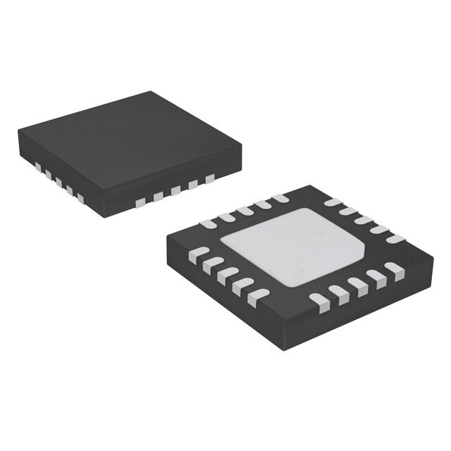
- 型号: LMH0346SQE/NOPB
- 制造商: Texas Instruments
- 库位|库存: xxxx|xxxx
- 要求:
| 数量阶梯 | 香港交货 | 国内含税 |
| +xxxx | $xxxx | ¥xxxx |
查看当月历史价格
查看今年历史价格
LMH0346SQE/NOPB产品简介:
ICGOO电子元器件商城为您提供LMH0346SQE/NOPB由Texas Instruments设计生产,在icgoo商城现货销售,并且可以通过原厂、代理商等渠道进行代购。 LMH0346SQE/NOPB价格参考¥138.01-¥213.15。Texas InstrumentsLMH0346SQE/NOPB封装/规格:线性 - 视频处理, Video IC 24-WQFN (4x5) Package。您可以下载LMH0346SQE/NOPB参考资料、Datasheet数据手册功能说明书,资料中有LMH0346SQE/NOPB 详细功能的应用电路图电压和使用方法及教程。
| 参数 | 数值 |
| 产品目录 | 集成电路 (IC)半导体 |
| 描述 | IC RECLOCKER HD/SD SDI 24LLP视频 IC 3Gbps HD/SD SDI Reclocker |
| 产品分类 | |
| 品牌 | Texas Instruments |
| 产品手册 | |
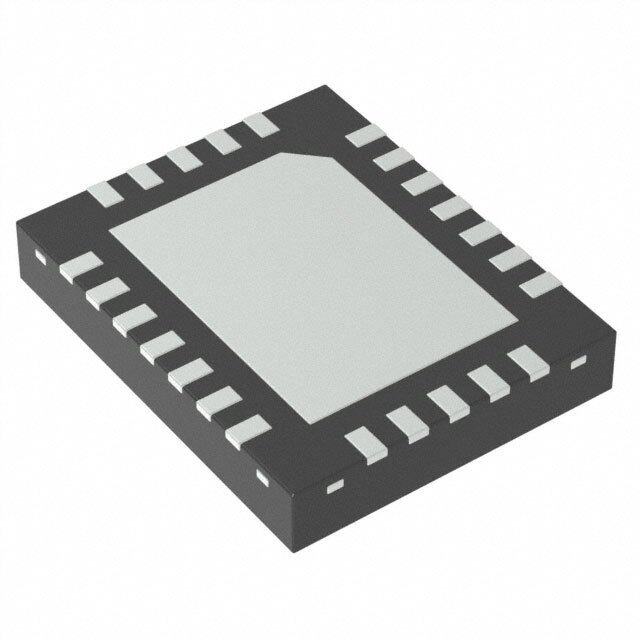
| 产品图片 |
|
| rohs | 符合RoHS无铅 / 符合限制有害物质指令(RoHS)规范要求 |
| 产品系列 | 多媒体 IC,视频 IC,Texas Instruments LMH0346SQE/NOPB- |
| 数据手册 | |
| 产品型号 | LMH0346SQE/NOPB |
| 产品目录页面 | |
| 产品种类 | 视频 IC |
| 供应商器件封装 | 24-WQFN (4x5) |
| 其它名称 | LMH0346SQE/NOPBDKR |
| 包装 | Digi-Reel® |
| 商标 | Texas Instruments |
| 安装类型 | 表面贴装 |
| 安装风格 | SMD/SMT |
| 封装 | Reel |
| 封装/外壳 | 24-WFQFN 裸露焊盘 |
| 封装/箱体 | WQFN-24 |
| 工作电源电压 | 3.3 V |
| 工厂包装数量 | 250 |
| 应用 | SDTV/HDTV |
| 最大功率耗散 | 370 mW |
| 最大工作温度 | + 85 C |
| 最小工作温度 | - 40 C |
| 标准包装 | 1 |
| 电源电流 | 111 mA |
| 类型 | 时钟恢复器 |
| 系列 | LMH0346 |
| 配用 | /product-detail/zh/SD3GDAEVK/SD3GDAEVK-ND/1678555/product-detail/zh/SD346EVK/SD346EVK-ND/1678554 |





- 商务部:美国ITC正式对集成电路等产品启动337调查
- 曝三星4nm工艺存在良率问题 高通将骁龙8 Gen1或转产台积电
- 太阳诱电将投资9.5亿元在常州建新厂生产MLCC 预计2023年完工
- 英特尔发布欧洲新工厂建设计划 深化IDM 2.0 战略
- 台积电先进制程称霸业界 有大客户加持明年业绩稳了
- 达到5530亿美元!SIA预计今年全球半导体销售额将创下新高
- 英特尔拟将自动驾驶子公司Mobileye上市 估值或超500亿美元
- 三星加码芯片和SET,合并消费电子和移动部门,撤换高东真等 CEO
- 三星电子宣布重大人事变动 还合并消费电子和移动部门
- 海关总署:前11个月进口集成电路产品价值2.52万亿元 增长14.8%



PDF Datasheet 数据手册内容提取
LMH0346 www.ti.com SNLS248J–APRIL2007–REVISEDAPRIL2013 3 Gbps HD/SD SDI Reclocker with Dual Differential Outputs CheckforSamples:LMH0346 FEATURES DESCRIPTION 1 • SupportsSMPTE424M,SMPTE292M,and The LMH0346 3 Gbps HD/SD SDI Reclocker retimes 2 serial digital video data conforming to the SMPTE SMPTE259M(C)SerialDigitalVideo 424M, SMPTE 292M, and SMPTE 259M (C) Standards standards. The LMH0346 operates at serial data • Supports270Mbps,1.483Gbps,1.485Gbps, rates of 270 Mbps, 1.483 Gbps, 1.485 Gbps, 2.967 2.967Gbps,and2.97GbpsSerialDataRate Gbps, and 2.97 Gbps. The LMH0346 supports DVB- Operation ASIoperationat270Mbps. • SupportsDVB-ASIat270Mbps The LMH0346 automatically detects the incoming • Single3.3VSupplyOperation data rate and adjusts itself to retime the incoming data to suppress accumulated jitter. The LMH0346 • 370mWTypicalPowerConsumption recovers the serial data-rate clock and optionally • TwoDifferential,ReclockedOutputs provides it as an output. The LMH0346 has two • ChoiceofSecondReclockedOutputorLow- differential serial data outputs; the second output may Jitter,Differential,Data-RateClockOutput be selected as a low-jitter, data-rate clock output. Controls and indicators are: serial clock or second • Single27MHzExternalCrystalorReference serial data output select, manual rate select input, ClockInput SD/HD rate indicator output, lock detect output, • ManualorAutomaticRateSelectInput auto/manual data bypass and output mute. The serial • SD/HDOperatingRateIndicatorOutput data inputs, outputs, and serial clock outputs are differential LVPECL compatible. The CML serial data • LockDetectIndicatorOutput and serial clock outputs are suitable for driving 100Ω • OutputMuteFunctionforDataandClock differentially terminated networks. The control logic • Auto/ManualReclockerBypass inputsandoutputsareLVCMOScompatible. • DifferentialLVPECLCompatibleSerialData The LMH0346 is powered from a single 3.3V supply. InputsandOutputs Powerdissipationistypically370mW. • LVCMOSControlInputsandIndicatorOutputs The device is available in two space-saving • 20-PinHTSSOPor24-PinWQFNPackage packages: a 6.5 X 4.4 mm 20-pin HTSSOP and an • IndustrialTemperatureRange:-40°Cto+85°C even more space–efficient 5 X 4 mm 24-pin WQFN package. • FootprintCompatibleWiththeLMH0046and LMH0026(HTSSOPPackage) APPLICATIONS • SDTV/HDTVand3GbpsSerialDigitalVideo Interfacesfor: – DigitalVideoRoutersandSwitchers – DigitalVideoProcessingandEditing Equipment – DVB-ASIEquipment – VideoStandardsandFormatConverters 1 Pleasebeawarethatanimportantnoticeconcerningavailability,standardwarranty,anduseincriticalapplicationsof TexasInstrumentssemiconductorproductsanddisclaimerstheretoappearsattheendofthisdatasheet. Alltrademarksarethepropertyoftheirrespectiveowners. 2 PRODUCTIONDATAinformationiscurrentasofpublicationdate. Copyright©2007–2013,TexasInstrumentsIncorporated Products conform to specifications per the terms of the Texas Instruments standard warranty. Production processing does not necessarilyincludetestingofallparameters.
LMH0346 SNLS248J–APRIL2007–REVISEDAPRIL2013 www.ti.com Typical Application CABLE DRIVER LMH0302 CABLE 3 Gbps/HD/SD EQUALIZER RECLOCKER LMH0344 LMH0346 CABLE DRIVER LMH0302 CABLE 3 Gbps/HD/SD EQUALIZER RECLOCKER LMH0344 LMH0346 3 Gbps/HD/SD SERIAL CROSSPOINT CABLE DRIVER DATA CABLE SWITCH 3 Gbps/HD/SD LMH0302 EQUALIZER RECLOCKER LMH0344 LMH0346 CABLE DRIVER LMH0302 CABLE 3 Gbps/HD/SD EQUALIZER RECLOCKER LMH0344 LMH0346 Block Diagram SCO_EN SD/HD BYPASS/AUTO BYPASS CONTROL LOGIC LOCK DETECT RATE0 RATE1 VCCO BYPASS 50 50 XTAL IN/EXT CLK XTAL OUT SCO/SDO2 VCO / PLL LOOP FILTER 1 SCO/SDO2 LOOP FILTER 2 VCCO O/P MUTE 50 50 SDO SDI RETIMER / FIFO SDI SDO 2 SubmitDocumentationFeedback Copyright©2007–2013,TexasInstrumentsIncorporated ProductFolderLinks:LMH0346
LMH0346 www.ti.com SNLS248J–APRIL2007–REVISEDAPRIL2013 Connection Diagram 1 20 LF1 SCO_EN 2 19 LF2 SD/HD 3 18 RATE0 VCCO 4 17 RATE1 SDO 5 16 6 SDI LMH0346MH SDO 15 SDI VCCO 7 14 VCC SCO/SDO2 8 13 BP/AUTO-BP SCO/SDO2 9 12 OP MUTE LOCK DET 10 11 XTAL IN/EXT CLK XTAL OUT Theexposeddieattachpadisthenegativeelectricalterminalforthisdevice.Itmustbeconnectedtothenegative powersupplyvoltage. Figure1. 20-PinHTSSOP SeePackageNumberPWP N E D LF1 VEE RSVD SCO_ HSD/ 24 23 22 21 20 LF2 1 19 VCCO RATE0 2 18 SDO RATE1 3 17 SDO LMH0346SQ SDI 4 (top view) 16 VCCO SDI 5 15 SCO/SDO2 VCC 6 14 SCO/SDO2 BP/AUTO-BP 7 13 LOCK DET 8 9 10 11 12 E K E E T T L E E U U C V V O M T L OP N/EX XTA L I A T X Theexposeddieattachpadistheprimarynegativeelectricalterminalforthisdevice.Itmustbeconnectedtothe negativepowersupplyvoltage. Figure2. 24-PinWQFN SeePackageNumberNHZ Copyright©2007–2013,TexasInstrumentsIncorporated SubmitDocumentationFeedback 3 ProductFolderLinks:LMH0346
LMH0346 SNLS248J–APRIL2007–REVISEDAPRIL2013 www.ti.com PINDESCRIPTIONS HTSSOP WQFN Name Description Pin Pin 1 24 LF1 LoopFilter. 2 1 LF2 LoopFilter. 3 2 RATE0 DataRateselectinput.Thispinhasaninternalpulldown. 4 3 RATE1 DataRateselectinput.Thispinhasaninternalpulldown. 5 4 SDI DataInputTrue. 6 5 SDI DataInputComplement. 7 6 V Positivepowersupply. CC Bypass/AutoBypassmodeselect.Bypassesreclockingwhenhigh.This 8 7 BYPASS/AUTOBYPASS pinhasaninternalpulldown. DataandClockOutputMuteInput.Mutestheoutputwhenlow.Thispin 9 8 OUTPUTMUTE hasaninternalpullup. 10 9 XTALIN/EXTCLK CrystalorExternalOscillatorInput. 11 12 XTALOUT CrystalOscillatorOutput. 12 13 LOCKDETECT PLLLockDetectOutput(activehigh). 13 14 SCO/SDO2 SerialClockorSerialDataOutput2Complement. 14 15 SCO/SDO2 SerialClockorSerialDataOutput2True. 15 16 V Positivepowersupply(OutputDriver). CCO 16 17 SDO DataOutputComplement. 17 18 SDO DataOutputTrue. 18 19 V Positivepowersupply(OutputDriver). CCO 19 20 SD/HD DataRateRangeOutput.OutputishighforSDandlowforHDor3G. SerialClockorSerialData2Outputselect.Setssecondoutputtooutput 20 21 SCO_EN theclockwhenhighandthedatawhenlow.Thispinhasaninternal pulldown. — 10,11,23 V Negativepowersupply. EE — 22 RSVD Reservedforfutureuse.Donotconnect. DAP DAP V ConnectexposedDAPtonegativepowersupply(ground). EE Thesedeviceshavelimitedbuilt-inESDprotection.Theleadsshouldbeshortedtogetherorthedeviceplacedinconductivefoam duringstorageorhandlingtopreventelectrostaticdamagetotheMOSgates. 4 SubmitDocumentationFeedback Copyright©2007–2013,TexasInstrumentsIncorporated ProductFolderLinks:LMH0346
LMH0346 www.ti.com SNLS248J–APRIL2007–REVISEDAPRIL2013 ABSOLUTE MAXIMUM RATINGS(1) SupplyVoltage(V –V ) 4.0V CC EE LogicInputVoltage(Vi) V −0.15VtoV +0.15V EE CC LogicInputCurrent(singleinput) Vi=V −0.15V −5mA EE Vi=V +0.15V +5mA CC LogicOutputVoltage(Vo) V −0.15VtoV +0.15V EE CC LogicOutputSource/SinkCurrent ±8mA SerialDataOutputSinkCurrent(I ) 24mA SDO PackageThermalResistance θ 20-pinHTSSOP 26.6°C/W JA θ 24-pinWQFN 33.0°C/W JA θ 20-pinHTSSOP 2.4°C/W JC θ 24-pinWQFN 3.2°C/W JC StorageTemperatureRange −65°Cto+150°C JunctionTemperature +125°C LeadTemperature(Soldering4Sec) +260°C(Pb-free) ESDRating HBM 8kV MM 400V CDM 2kV (1) “AbsoluteMaximumRatings”arethoseparametervaluesbeyondwhichthelifeandoperationofthedevicecannotbeensured.The statinghereinofthesemaximumsshallnotbeconstruedtoimplythatthedevicecanorshouldbeoperatedatorbeyondthesevalues. DCELECTRICALCHARACTERISTICSandACELECTRICALCHARACTERISTICSspecifyacceptabledeviceoperatingconditions. RECOMMENDED OPERATING CONDITIONS SupplyVoltage(V –V ) 3.3V±5% CC EE LogicInputVoltage V toV EE CC DifferentialSerialInputVoltage 800mV±10% SerialDataorClockOutputSinkCurrent(I ) 16mAmax. SO OperatingFreeAirTemperature(T ) −40°Cto+85°C A Copyright©2007–2013,TexasInstrumentsIncorporated SubmitDocumentationFeedback 5 ProductFolderLinks:LMH0346
LMH0346 SNLS248J–APRIL2007–REVISEDAPRIL2013 www.ti.com DC ELECTRICAL CHARACTERISTICS OverSupplyVoltageandOperatingTemperatureranges,unlessotherwisespecified.(1)(2) Symbol Parameter Conditions Reference Min Typ Max Units V InputVoltageHighLevel Logicinputs 2 V V IH CC V InputVoltageLowLevel V 0.8 V IL EE I InputCurrentHighLevel V =V 47 65 µA IH IH CC I InputCurrentLowLevel V =V −18 −25 µA IL IL EE V OutputVoltageHighLevel I =−2mA Logicoutputs 2 V OH OH V OutputVoltageLowLevel I =+2mA V +0.6 V OL OL EE V SerialInputVoltage, See(3) SDI SDID 200 1600 mV Differential P-P V InputCommonMode V =200mV(3) CMI SDID V +0.95 V −0.2 V Voltage EE CC V SerialDataOutput 100Ωdifferentialload SDO,SDO2 SDOD 620 750 880 mV Voltage,Differential P-P V SerialClockOutput 100Ωdifferentialload, SCO SCOD Voltage,Differential 2970MHz(3) 400 525 650 mVP-P 100Ωdifferentialload, 750 mV 1485or270MHzMbps P-P V OutputCommonMode 100Ωdifferentialload SDO,SCO V − CMO CC V Voltage V SDOD I SupplyCurrent 2970Mbps 111 126 mA CC (1) Currentflowintodevicepinsisdefinedaspositive.Currentflowoutofdevicepinsisdefinedasnegative.Allvoltagesarereferencedto V (equaltozerovolts). EE (2) Typicalvaluesarestatedfor:V =+3.3V,T =+25°C. CC A (3) Thisparameterisensuredbycharacterizationovervoltageandtemperaturelimits. 6 SubmitDocumentationFeedback Copyright©2007–2013,TexasInstrumentsIncorporated ProductFolderLinks:LMH0346
LMH0346 www.ti.com SNLS248J–APRIL2007–REVISEDAPRIL2013 AC ELECTRICAL CHARACTERISTICS OverSupplyVoltageandOperatingTemperatureranges,unlessotherwisespecified.(1) Symbol Parameter Conditions Reference Min Typ Max Units BR SerialDataRate SMPTE259M,C SDI,SDO 270 Mbps SD BR SerialDataRate SMPTE292M 1483, SD Mbps 1485 BR SerialDataRate SMPTE424M 2967, SD Mbps 2970 TOL SerialInputJitter 270Mbps(2)(3)(4) SDI JIT >6 UI Tolerance P-P TOL SerialInputJitter 270Mbps(2)(3)(5) JIT >0.6 UI Tolerance P-P TOL SerialInputJitter 1483or1485Mbps(2)(3)(4) JIT >6 UI Tolerance P-P TOL SerialInputJitter 1483or1485Mbps(2)(3)(5) JIT >0.6 UI Tolerance P-P TOL SerialInputJitter 2967or2970Mbps(2)(3)(4) JIT >6 UI Tolerance P-P TOL SerialInputJitter 2967or2970Mbps(2)(3)(5) JIT >0.6 UI Tolerance P-P t SerialDataOutputJitter 270Mbps(3)(6) SDO 0.01 0.03 UI JIT P-P t SerialDataOutputJitter 1483or1485Mbps(3)(7) 0.03 0.04 UI JIT P-P t SerialDataOutputJitter 2967or2970Mbps(3)(8) 0.06 0.08 UI JIT P-P BW LoopBandwidth 270Mbps, LOOP 275 kHz <0.1dBPeaking 1485Mbps, 1.5 MHz <0.1dBPeaking 2970Mbps, 2.75 MHz <0.1dBPeaking F SerialClockOutput 270Mbpsdatarate SCO CO 270 MHz Frequency F SerialClockOutput 1483Mbpsdatarate CO 1483 MHz Frequency F SerialClockOutput 1485Mbpsdatarate CO 1485 MHz Frequency F SerialClockOutput 2967Mbpsdatarate CO 2967 MHz Frequency F SerialClockOutput 2970Mbpsdatarate CO 2970 MHz Frequency t SerialClockOutputJitter 2 3 ps JIT RMS SerialClockOutput See(3) SDO,SCO Alignmentwithrespectto 40 60 % DataInterval SerialClockOutputDuty See(3) SCO 45 55 % Cycle T AcquisitionTime See(9) 15 ms ACQ t,t Inputrise/falltime 10%–90% Logicinputs 1.5 ns r f (1) Typicalvaluesarestatedfor:V =+3.3V,T =+25°C. CC A (2) Peak-to-peakamplitudewithsinusoidalmodulationperSMPTERP184-1996paragraph4.1.Thetestdatasignalshallbecolorbars. (3) Thisparameterisensuredbycharacterizationovervoltageandtemperaturelimits. (4) Referto“A1”inFigure1ofSMPTERP184-1996. (5) Referto“A2”inFigure1ofSMPTERP184-1996. (6) PRBS210−1,inputjitter=31ps P-P (7) PRBS210−1,inputjitter=24ps P-P (8) PRBS210−1,inputjitter=22ps P-P (9) MeasuredfromfirstSDItransitionuntilLockDetect(LD)outputgoeshigh(true). Copyright©2007–2013,TexasInstrumentsIncorporated SubmitDocumentationFeedback 7 ProductFolderLinks:LMH0346
LMH0346 SNLS248J–APRIL2007–REVISEDAPRIL2013 www.ti.com AC ELECTRICAL CHARACTERISTICS (continued) OverSupplyVoltageandOperatingTemperatureranges,unlessotherwisespecified.(1) Symbol Parameter Conditions Reference Min Typ Max Units t,t Inputrise/falltime 20%–80%,270Mbps(10) SDI 1500 ps r f t,t Inputrise/falltime 20%–80%,1483or1485 r f Mbps(10) 270 ps t,t Inputrise/falltime 20%–80%,2967or2970 r f Mbps(10) 135 ps t,t Outputrise/falltime 10%–90% Logicoutputs 1.5 ns r f t,t Outputrise/falltime 20%–80%(3)(11) SDO,SCO 90 130 ps r f F ReferenceClock REF 27 MHz Frequency F ReferenceClock TOL ±50 ppm FrequencyTolerance (10) Thisspecificationisensuredbydesign. (11) R =100Ωdifferential. L 8 SubmitDocumentationFeedback Copyright©2007–2013,TexasInstrumentsIncorporated ProductFolderLinks:LMH0346
LMH0346 www.ti.com SNLS248J–APRIL2007–REVISEDAPRIL2013 DEVICE DESCRIPTION The LMH0346 3 Gbps HD/SD SDI Reclocker is used in many types of digital video signal processing equipment. SupportedserialdigitalvideostandardsareSMPTE259M(C),SMPTE292M,andSMPTE424M.Corresponding serial data rates are 270 Mbps, 1.483 Gbps, 1.485 Gbps, 2.967 Gbps, and 2.97 Gbps. DVB-ASI data at 270 Mbps may also be retimed. The LMH0346 retimes the serial data stream to suppress accumulated jitter. It provides two low-jitter, differential, serial data outputs. The second output may be selected to output either serial data or a low-jitter serial data-rate clock. Controls and indicators are: serial clock or second serial data output select, manual rate select input, SD/HD rate output, lock detect output, auto/manual data bypass and output mute. Serial data inputs are CML and LVPECL compatible. Serial data and clock outputs are differential CML and produce LVPECL compatible levels. The output buffer design can drive AC or DC-coupled, terminated 100Ω differential loads. The differential output level is 750 mV into 100Ω AC or DC-coupled differential loads. Logic P-P inputsandoutputsareLVCMOScompatible. The device package is a 20-pin HTSSOP or a 24-pin WQFN. Both package options have an exposed die attach pad. The exposed die attach pad is electrically connected to device ground (V ) and is the negative electrical EE terminalforthedevice.Thisterminalmustbeconnectedtothenegativepowersupplyorcircuitground. Serial Data Inputs, Serial Data and Clock Outputs SERIALDATAINPUTANDOUTPUTS The differential serial data input, SDI, accepts serial digital video data at the rates specified in Table 1. The serial data input is differential LVPECL compatible. The input is intended to be DC interfaced to devices such as the LMH0344 adaptive cable equalizer. The input is not internally terminated or biased. The input may be AC- coupledifasuitableinputbiasvoltageisprovided.Figure3showstheequivalentinputcircuitforSDIandSDI. The LMH0346 has two, retimed, differential, serial data outputs, SDO and SCO/SDO2. These outputs provide low jitter, differential, retimed data to devices such as the LMH0302 cable driver. Output SCO/SDO2 is multiplexed and can provide either a second serial data output or a serial clock output. Figure 4 shows the equivalentoutputcircuitforSDO,SDO,SCO/SDO2,andSCO/SDO2. The SCO_EN input controls the operating mode for the SCO/SDO2 output. When the SCO_EN input is high the SCO/SDO2 output provides a serial clock. When SCO_EN is low, the SCO/SDO2 output provides retimed serial data. Both differential serial data outputs, SDO and SCO/SDO2, are muted when the OUTPUT MUTE input is a logic low level. SCO/SDO2 also mutes when the Bypass mode is activated and this output is operating as the serial clock output (SCO_EN input is high). When muted, SDO and SDO (or SDO2 and SDO2) will assume opposite differential output levels. The CML serial data outputs are differential LVPECL compatible. These outputs have internal 50Ω pull-ups and are suitable for driving AC or DC-coupled, 100Ω center-tapped, AC grounded or 100Ω un-center-tapped,differentiallyterminatednetworks. Copyright©2007–2013,TexasInstrumentsIncorporated SubmitDocumentationFeedback 9 ProductFolderLinks:LMH0346
LMH0346 SNLS248J–APRIL2007–REVISEDAPRIL2013 www.ti.com VCC 20 k: 1 pF 80 k: VCC 2 k: 2 k: VCC SDI SDI Figure3. EquivalentSDIInputCircuit(SDI,SDI) VCC VCC VCC 50: 50: SDO, SCO/SDO2 SDO, SCO/SDO2 Figure4. EquivalentSDOOutputCircuit(SDO,SDO,SCO/SDO2,SCO/SDO2) OPERATINGSERIALDATARATES This device operates at serial data rates of 270 Mbps, 1483 Mbps, 1485 Mbps, 2967 Mbps, and 2970 Mbps. The device does not lock to harmonics of these rates. The device does not lock and automatically enters the reclockerbypassmodeforthefollowingdatarates:143Mbps,177Mbps,360Mbps,and540Mbps. SERIALDATACLOCK/SERIALDATA2OUTPUT The Serial Data Clock/Serial Data 2 Output is controlled by the SCO_EN input and provides either a second retimed serial data output or a low jitter differential clock output appropriate to the serial data rate being processed. When operating as a serial clock output, the rising edge of the clock will be positioned within the correspondingserialdatabitintervalwithin10%ofthecenterofthedatainterval. 10 SubmitDocumentationFeedback Copyright©2007–2013,TexasInstrumentsIncorporated ProductFolderLinks:LMH0346
LMH0346 www.ti.com SNLS248J–APRIL2007–REVISEDAPRIL2013 Differential output SCO/SDO2 functions as the second serial data output when the SCO_EN input is a logic-low level. This output functions as the serial clock output when the SCO_EN input is a logic-high level. The SCO_EN input has an internal pull-down device and the default state of SCO_EN is low (serial data output 2 enabled). SCO/SDO2 is muted when the OUTPUT MUTE input is a logic low level. When the Bypass mode is activated and this output is functioning as a serial clock output (SCO_EN is high), the output will also be muted. If an unsupporteddatarateisusedwhileinAutoBypassmodewiththisoutputfunctioningasaserialclockoutput,the outputisinvalid. Control Inputs and Indicator Outputs SERIALDATARATESELECTOR The Serial Data Rate Selector (RATE [1:0]) permits the user to fix the operating serial data rate. The pins have internal pull-downs which maintain a logic-low input condition unless externally driven to a logic-high condition. This input also serves to place the device in a test mode. The codes shown in Table 1 select the desired operatingserialdatarate.TheLMH0346thenenterseithertheAuto-RateDetectmodeorasingleoperatingrate. Selecting the 270 Mbps rate mode may also be used when reclocking DVB-ASI data. DVB-ASI data is MPEG2 coded data that is transmitted in 8B10B coding. The device will reclock this data without harmonic locking. Auto- RateDetectmodemaybeusedforanysupporteddatarate,includingDVB-ASI. Table1.DataRateSelectInputCodes Rate[1:0]Code DataRateorMode Comments 00 Auto-RateDetectmode 01 270Mbps MaybeusedtosupportDVB-ASIoperation 10 1483/1485Mbps,2967/2970Mbps LOCKDETECT The Lock Detect (LD) output, when high, indicates that data is being received and the PLL is locked. LD may be connected to the OUTPUT MUTE input to mute the data and clock outputs when no data signal is being received.NotethatwhentheBypass/AutoBypassinputissethigh,LockDetectwillremainlow.SeeTable2. OUTPUTMUTE The OUTPUT MUTE input, when low, mutes the serial data and clock outputs. It may be connected to Lock Detect or externally driven to mute or un-mute the outputs. If OUTPUT MUTE is connected to LD, then the data and clock outputs are muted when the PLL is not locked. This function overrides the Bypass function: see Table2.OUTPUTMUTEhasaninternalpull-updevicetoenabletheoutputbydefault. BYPASS/AUTOBYPASS The Bypass/Auto Bypass input, when high, forces the device to output the data without reclocking it. When this input is low, the device automatically bypasses the reclocking function when the device is in an unlocked condition or the detected data rate is a rate which the device does not support. Note that when the Bypass/Auto Bypassinputissethigh,LockDetectwillremainlow.SeeTable2.BYPASS/AUTOBYPASShasaninternalpull- downdevice. Table2.ControlFunctionality LOCKDETECT OUTPUTMUTE BYPASS/AUTOBYPASS DEVICESTATUS 0 1 X PLLunlocked,reclockerbypassed 1 1 0 PLLlockedtosupporteddatarate,reclockernotbypassed X 0 X Outputsmuted 0 LOCKDETECT X Outputsmuted 1 LOCKDETECT 0 PLLlockedtosupporteddatarate,reclockernotbypassed Copyright©2007–2013,TexasInstrumentsIncorporated SubmitDocumentationFeedback 11 ProductFolderLinks:LMH0346
LMH0346 SNLS248J–APRIL2007–REVISEDAPRIL2013 www.ti.com SD/HD The SD/HD output indicates whether the LMH0346 is processing SD or HD / 3 Gbps data rates. It may be used to control another device such as the LMH0302 cable driver. When this output is high it indicates that the data rate is 270 Mbps. When low, the indicated data rate is 1483, 1485, 2967, or 2970 Mbps. The SD/HD output is a registered function and is only valid when the PLL is locked and the Lock Detect output is high. When the PLL is not locked (the Lock Detect output is low), the SD/HD output defaults to HD (low). The SD/HD output is undefined for a short time after lock detect assertion or deassertion due to a data rate change on SDI. See Figure5foratimingdiagramshowingtherelationshipbetweenSDI,LockDetect,andSD/HD. SDI NO DATA 270 MBPS DATA NO DATA 1485 MBPS DATA NO DATA TACQ T2 TACQ T2 Lock Detect T1 T1 T1 SD/HD SDI NO DATA 270 MBPS DATA 1485 MBPS DATA 2970 MBPS DATA 270 MBPS DATA TACQ TACQ TACQ TACQ T2 T2 T2 Lock Detect T1 T1 T1 T1 T1 SD/HD TACQ = Acquisition Time, defined in the AC Electrical Characteristics Table T1 = Time from Lock Detect assertion or deassertion until SD/HD output is valid, typically 37 ns (one 27 MHz clock period) T2 = Time from SDI input change until Lock Detect de-assertion, 1 ms maximum. SD/HD output is not valid during this time. Figure5. SDI,LockDetect,andSD/HDTiming SCO_EN Input SCO_EN enables the SCO/SDO2 differential output to function either as a serial clock or second serial data output. SCO/SDO2 functions as a serial clock when SCO_EN is high. This pin has an internal pull-down device.Thedefaultstate(low)enablestheSCO/SDO2outputasasecondserialdataoutput. 12 SubmitDocumentationFeedback Copyright©2007–2013,TexasInstrumentsIncorporated ProductFolderLinks:LMH0346
LMH0346 www.ti.com SNLS248J–APRIL2007–REVISEDAPRIL2013 CRYSTALOREXTERNALCLOCKREFERENCE The LMH0346 uses a 27 MHz crystal or external clock signal as a timing reference input. A 27 MHz parallel resonant crystal and load network may be connected to the XTAL IN/EXT CLK and XTAL OUT pins. Alternatively, a 27 MHz LVCMOS compatible clock signal may be input to XTAL IN/EXT CLK. Parameters for a suitablecrystalaregiveninTable3. Table3.CrystalParameters Parameter Value Frequency 27MHz FrequencyStability ±50ppm@recommendeddrivelevel OperatingMode Fundamentalmode,ParallelResonant LoadCapacitance 18–20pF ShuntCapacitance 7pF SeriesResistance 40Ωmax. RecommendedDriveLevel 100µW MaximumDriveLevel 500µW OperatingTemperatureRange −10°Cto+60°C Copyright©2007–2013,TexasInstrumentsIncorporated SubmitDocumentationFeedback 13 ProductFolderLinks:LMH0346
LMH0346 SNLS248J–APRIL2007–REVISEDAPRIL2013 www.ti.com APPLICATION INFORMATION Figure 6 shows an application circuit for the LMH0346 along with the LMH0344 3 Gbps HD/SD SDI Adaptive CableEqualizerandLMH03023GbpsHD/SDSDICableDriver. VCC VCC RATE0 56 nF RATE1 SCO_EN 1 20 LF1 SCO_EN 2 19 LMH0344 Adaptive 3 LF2 SD/HD 18 A Cable Equalizer RATE0 VCCO Coaxial Cable 75: 1.0 PF 4 RATE1 SDO 17 B 5 16 SDI SDO 6 SDI LMH0346 SDO 15 C 100: 7 SDI VCCO 14 1.0 PF VCC SCO/SDO2 Additional 6.8 nH SDI SDO 8 BP/AUTO-BP SCO/SDO2 13 Outputs 9 12 OP MUTE LOCK DET 10 11 75: 37.4: EC+ EC- XTAL IN/EXT CLK XTAL OUT A A DAP 27 MHz 1.0 PF BP/AUTO-BP 39 pF 39 pF LOCK DET OP MUTE +3.3V A 75: 75: 5.6 nH LMH0302 Cable Driver SD/HD 75: 4.7 PF Coaxial Cable B SDI SDO 100: SDO 75: 4.7 PF Coaxial Cable 75: C SDI RREF 75: +3.3V 5.6 nH 750: Figure6. ApplicationCircuit The LMH0346 inputs are LVPECL compatible. The LMH0346 has a wide input common mode range and in most cases the input should be DC coupled. For DC coupling, the inputs must be kept within the common mode range specified in DC ELECTRICAL CHARACTERISTICS. Figure 6 shows an example of a DC coupled interface between the LMH0344 cable equalizer and the LMH0346. The LMH0344 output common mode voltage and voltage swing are within the range of the input common mode voltage and voltage swing of the LMH0346. All that is required is a 100Ω differential termination as shown. The resistor should be placed as close to the LMH0346 input as possible. If desired, this network may be terminated with two 50Ω resisters and a center tap capacitortogroundinplaceofthesingle100Ω resistor. 14 SubmitDocumentationFeedback Copyright©2007–2013,TexasInstrumentsIncorporated ProductFolderLinks:LMH0346
LMH0346 www.ti.com SNLS248J–APRIL2007–REVISEDAPRIL2013 The LMH0346 outputs are LVPECL compatible. SDO is the primary data output and SCO/SDO2 is a second outputthatmaybesetastheserialclockoraseconddataoutput.Bothoutputsarealwaysactive.TheLMH0346 output should be DC coupled to the input of the receiving device as long as the common mode ranges of both devices are compatible. Figure 6 shows an example of a DC coupled interface between the LMH0346 and LMH0302 cable driver. All that is required is a 100Ω differential termination as shown. The resistor should be placed as close to the LMH0302 input as possible. If desired, this network may be terminated with two 50Ω resistersandacentertapcapacitortogroundinplaceofthesingle100Ω resistor. The external loop filter capacitor (between LF1 and LF2) should be 56 nF. This is the only supported value; the loopfiltercapacitorshouldnotbechanged. RATE0 and RATE1 have internal pulldowns to select Auto-Rate Detect mode by default. These pins may also be usedtosetthedevicetoSDmodeorHD/3Gmode. BYPASS/AUTO BYPASS has an internal pulldown to enable Auto Bypass mode by default. This pin may be pulledhightoforcetheLMH0346tobypassalldata. OUTPUT MUTE has an internal pullup to enable the outputs by default. This pin may be pulled low to mute the outputs. TheXTALIN/EXTCLKandXTALOUTpinsareshownwitha27MHzcrystalandtheproperloading.Thecrystal should match the parameters described in Table 3. Alternately, a 27MHz LVCMOS compatible clock signal may beinputtoXTALIN/EXTCLK. The active high LOCK DETECT output provides an indication that proper data is being received and the PLL is locked. TheSD/HDoutputmaybeusedtodrivetheSD/HDpinofanSDIcabledriver(suchastheLMH0302)inorderto properly set the cable driver’s edge rate for SMPTE compliance. It defaults to HD/3G (low) when the LMH0346 is notlocked. SCO_EN has an internal pulldown to set the second output (SCO/SDO2) to output data. This pin may be pulled hightosetthesecondoutputasaserialclock. The ground connection for the LMH0346 is through the large exposed DAP. The DAP must be connected to ground for proper operation of the LMH0346. This is the only ground connection for the LMH0346MH. It is the primarygroundconnection,requiredforgoodsignalintegrity,fortheLMH0346SQ. Copyright©2007–2013,TexasInstrumentsIncorporated SubmitDocumentationFeedback 15 ProductFolderLinks:LMH0346
LMH0346 SNLS248J–APRIL2007–REVISEDAPRIL2013 www.ti.com REVISION HISTORY ChangesfromRevisionI(April2013)toRevisionJ Page • ChangedlayoutofNationalDataSheettoTIformat.......................................................................................................... 15 16 SubmitDocumentationFeedback Copyright©2007–2013,TexasInstrumentsIncorporated ProductFolderLinks:LMH0346
PACKAGE OPTION ADDENDUM www.ti.com 6-Feb-2020 PACKAGING INFORMATION Orderable Device Status Package Type Package Pins Package Eco Plan Lead/Ball Finish MSL Peak Temp Op Temp (°C) Device Marking Samples (1) Drawing Qty (2) (6) (3) (4/5) LMH0346MH/NOPB ACTIVE HTSSOP PWP 20 73 Green (RoHS SN Level-3-260C-168 HR -40 to 85 L0346 & no Sb/Br) LMH0346MHX/NOPB ACTIVE HTSSOP PWP 20 2500 Green (RoHS SN Level-3-260C-168 HR -40 to 85 L0346 & no Sb/Br) LMH0346SQ/NOPB ACTIVE WQFN NHZ 24 1000 Green (RoHS SN Level-3-260C-168 HR -40 to 85 L0346SQ & no Sb/Br) LMH0346SQE/NOPB ACTIVE WQFN NHZ 24 250 Green (RoHS SN Level-3-260C-168 HR -40 to 85 L0346SQ & no Sb/Br) (1) The marketing status values are defined as follows: ACTIVE: Product device recommended for new designs. LIFEBUY: TI has announced that the device will be discontinued, and a lifetime-buy period is in effect. NRND: Not recommended for new designs. Device is in production to support existing customers, but TI does not recommend using this part in a new design. PREVIEW: Device has been announced but is not in production. Samples may or may not be available. OBSOLETE: TI has discontinued the production of the device. (2) RoHS: TI defines "RoHS" to mean semiconductor products that are compliant with the current EU RoHS requirements for all 10 RoHS substances, including the requirement that RoHS substance do not exceed 0.1% by weight in homogeneous materials. Where designed to be soldered at high temperatures, "RoHS" products are suitable for use in specified lead-free processes. TI may reference these types of products as "Pb-Free". RoHS Exempt: TI defines "RoHS Exempt" to mean products that contain lead but are compliant with EU RoHS pursuant to a specific EU RoHS exemption. Green: TI defines "Green" to mean the content of Chlorine (Cl) and Bromine (Br) based flame retardants meet JS709B low halogen requirements of <=1000ppm threshold. Antimony trioxide based flame retardants must also meet the <=1000ppm threshold requirement. (3) MSL, Peak Temp. - The Moisture Sensitivity Level rating according to the JEDEC industry standard classifications, and peak solder temperature. (4) There may be additional marking, which relates to the logo, the lot trace code information, or the environmental category on the device. (5) Multiple Device Markings will be inside parentheses. Only one Device Marking contained in parentheses and separated by a "~" will appear on a device. If a line is indented then it is a continuation of the previous line and the two combined represent the entire Device Marking for that device. (6) Lead/Ball Finish - Orderable Devices may have multiple material finish options. Finish options are separated by a vertical ruled line. Lead/Ball Finish values may wrap to two lines if the finish value exceeds the maximum column width. Important Information and Disclaimer:The information provided on this page represents TI's knowledge and belief as of the date that it is provided. TI bases its knowledge and belief on information provided by third parties, and makes no representation or warranty as to the accuracy of such information. Efforts are underway to better integrate information from third parties. TI has taken and Addendum-Page 1
PACKAGE OPTION ADDENDUM www.ti.com 6-Feb-2020 continues to take reasonable steps to provide representative and accurate information but may not have conducted destructive testing or chemical analysis on incoming materials and chemicals. TI and TI suppliers consider certain information to be proprietary, and thus CAS numbers and other limited information may not be available for release. In no event shall TI's liability arising out of such information exceed the total purchase price of the TI part(s) at issue in this document sold by TI to Customer on an annual basis. Addendum-Page 2
PACKAGE MATERIALS INFORMATION www.ti.com 20-Sep-2016 TAPE AND REEL INFORMATION *Alldimensionsarenominal Device Package Package Pins SPQ Reel Reel A0 B0 K0 P1 W Pin1 Type Drawing Diameter Width (mm) (mm) (mm) (mm) (mm) Quadrant (mm) W1(mm) LMH0346MHX/NOPB HTSSOP PWP 20 2500 330.0 16.4 6.95 7.1 1.6 8.0 16.0 Q1 LMH0346SQ/NOPB WQFN NHZ 24 1000 178.0 12.4 4.3 5.3 1.3 8.0 12.0 Q1 LMH0346SQE/NOPB WQFN NHZ 24 250 178.0 12.4 4.3 5.3 1.3 8.0 12.0 Q1 PackMaterials-Page1
PACKAGE MATERIALS INFORMATION www.ti.com 20-Sep-2016 *Alldimensionsarenominal Device PackageType PackageDrawing Pins SPQ Length(mm) Width(mm) Height(mm) LMH0346MHX/NOPB HTSSOP PWP 20 2500 367.0 367.0 38.0 LMH0346SQ/NOPB WQFN NHZ 24 1000 210.0 185.0 35.0 LMH0346SQE/NOPB WQFN NHZ 24 250 210.0 185.0 35.0 PackMaterials-Page2
MECHANICAL DATA PWP0020A MXA20A (Rev C) www.ti.com
MECHANICAL DATA NHZ0024B SQA24B (Rev A) www.ti.com
IMPORTANTNOTICEANDDISCLAIMER TI PROVIDES TECHNICAL AND RELIABILITY DATA (INCLUDING DATASHEETS), DESIGN RESOURCES (INCLUDING REFERENCE DESIGNS), APPLICATION OR OTHER DESIGN ADVICE, WEB TOOLS, SAFETY INFORMATION, AND OTHER RESOURCES “AS IS” AND WITH ALL FAULTS, AND DISCLAIMS ALL WARRANTIES, EXPRESS AND IMPLIED, INCLUDING WITHOUT LIMITATION ANY IMPLIED WARRANTIES OF MERCHANTABILITY, FITNESS FOR A PARTICULAR PURPOSE OR NON-INFRINGEMENT OF THIRD PARTY INTELLECTUAL PROPERTY RIGHTS. These resources are intended for skilled developers designing with TI products. You are solely responsible for (1) selecting the appropriate TI products for your application, (2) designing, validating and testing your application, and (3) ensuring your application meets applicable standards, and any other safety, security, or other requirements. These resources are subject to change without notice. TI grants you permission to use these resources only for development of an application that uses the TI products described in the resource. Other reproduction and display of these resources is prohibited. No license is granted to any other TI intellectual property right or to any third party intellectual property right. TI disclaims responsibility for, and you will fully indemnify TI and its representatives against, any claims, damages, costs, losses, and liabilities arising out of your use of these resources. TI’s products are provided subject to TI’s Terms of Sale (www.ti.com/legal/termsofsale.html) or other applicable terms available either on ti.com or provided in conjunction with such TI products. TI’s provision of these resources does not expand or otherwise alter TI’s applicable warranties or warranty disclaimers for TI products. Mailing Address: Texas Instruments, Post Office Box 655303, Dallas, Texas 75265 Copyright © 2020, Texas Instruments Incorporated

 Datasheet下载


