ICGOO在线商城 > 集成电路(IC) > 线性 - 放大器 - 仪表,运算放大器,缓冲器放大器 > LM8261M5
 Datasheet下载
- 型号: LM8261M5
- 制造商: Texas Instruments
- 库位|库存: xxxx|xxxx
- 要求:
| 数量阶梯 | 香港交货 | 国内含税 |
| +xxxx | $xxxx | ¥xxxx |
查看当月历史价格
查看今年历史价格
LM8261M5产品简介:
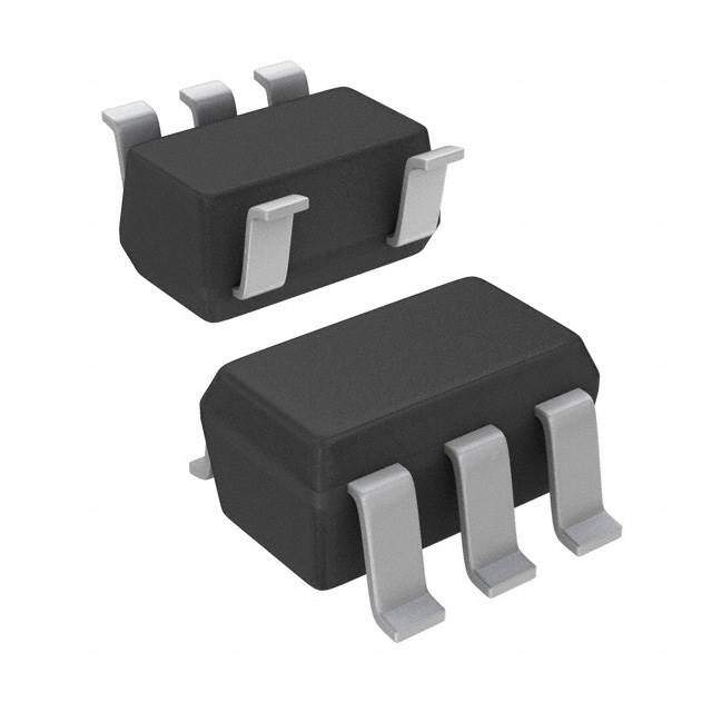
ICGOO电子元器件商城为您提供LM8261M5由Texas Instruments设计生产,在icgoo商城现货销售,并且可以通过原厂、代理商等渠道进行代购。 LM8261M5价格参考¥5.15-¥6.43。Texas InstrumentsLM8261M5封装/规格:线性 - 放大器 - 仪表,运算放大器,缓冲器放大器, 通用 放大器 1 电路 满摆幅 SOT-23-5。您可以下载LM8261M5参考资料、Datasheet数据手册功能说明书,资料中有LM8261M5 详细功能的应用电路图电压和使用方法及教程。
| 参数 | 数值 |
| -3db带宽 | - |
| 产品目录 | 集成电路 (IC) |
| 描述 | IC OPAMP GP 24MHZ RRO SOT23-5 |
| 产品分类 | Linear - Amplifiers - Instrumentation, OP Amps, Buffer Amps |
| 品牌 | Texas Instruments |
| 数据手册 | |
| 产品图片 |
|
| 产品型号 | LM8261M5 |
| rohs | 含铅 / 不符合限制有害物质指令(RoHS)规范要求 |
| 产品系列 | - |
| 产品培训模块 | http://www.digikey.cn/PTM/IndividualPTM.page?site=cn&lang=zhs&ptm=26100 |
| 供应商器件封装 | SOT-23-5 |
| 其它名称 | LM8261M5DKR |
| 制造商产品页 | http://www.ti.com/general/docs/suppproductinfo.tsp?distId=10&orderablePartNumber=LM8261M5 |
| 包装 | Digi-Reel® |
| 压摆率 | 15 V/µs |
| 增益带宽积 | 24MHz |
| 安装类型 | 表面贴装 |
| 封装/外壳 | SC-74A,SOT-753 |
| 工作温度 | -40°C ~ 85°C |
| 放大器类型 | 通用 |
| 标准包装 | 1 |
| 电压-电源,单/双 (±) | 2.5 V ~ 30 V, ±1.25 V ~ 15 V |
| 电压-输入失调 | 700µV |
| 电流-电源 | 1.3mA |
| 电流-输入偏置 | 1.05µA |
| 电流-输出/通道 | 100mA |
| 电路数 | 1 |
| 设计资源 | http://www.digikey.com/product-highlights/cn/zh/texas-instruments-webench-design-center/3176 |
| 输出类型 | 满摆幅 |


- 商务部:美国ITC正式对集成电路等产品启动337调查
- 曝三星4nm工艺存在良率问题 高通将骁龙8 Gen1或转产台积电
- 太阳诱电将投资9.5亿元在常州建新厂生产MLCC 预计2023年完工
- 英特尔发布欧洲新工厂建设计划 深化IDM 2.0 战略
- 台积电先进制程称霸业界 有大客户加持明年业绩稳了
- 达到5530亿美元!SIA预计今年全球半导体销售额将创下新高
- 英特尔拟将自动驾驶子公司Mobileye上市 估值或超500亿美元
- 三星加码芯片和SET,合并消费电子和移动部门,撤换高东真等 CEO
- 三星电子宣布重大人事变动 还合并消费电子和移动部门
- 海关总署:前11个月进口集成电路产品价值2.52万亿元 增长14.8%


PDF Datasheet 数据手册内容提取
Product Sample & Technical Tools & Support & Folder Buy Documents Software Community LM8261 SNOS469J–APRIL2000–REVISEDJANUARY2015 LM8261 Single RRIO High Output Current & Unlimited Cap Load Op Amp 1 Features 3 Description • (V = 5 V, T = 25°C, Typical Values Unless The LM8261 is a Rail-to-Rail input and output Op 1 S A Amp which can operate with a wide supply voltage Specified) range. This device has high output current drive, • GBWP21MHz greater than Rail-to-Rail input common mode voltage • WideSupplyVoltageRange2.5Vto30V range, unlimited capacitive load drive capability, and • SlewRate12V/µs provides tested and guaranteed high speed and slew rate while requiring only 0.97 mA supply current. It is • SupplyCurrent0.97mA specifically designed to handle the requirements of • CapLoadLimitUnlimited flat panel TFT panel V driver applications as well COM • OutputShortCircuitCurrent53mA/−75mA as being suitable for other low power, and medium speed applications which require ease of use and • ±5%SettlingTime400ns(500pF,100mV PP enhancedperformanceoverexistingdevices. Step) • InputCommonModeVoltage0.3VBeyondRails Greater than Rail-to-Rail input common mode voltage range with 50 dB of Common Mode Rejection allows • InputVoltageNoise15nV/√Hz high side and low side sensing, among many • InputCurrentNoise1pA/√Hz applications, without concern over exceeding the • THD+N <0.05% range and with no compromise in accuracy. Exceptionally wide operating supply voltage range of 2 Applications 2.5 V to 30 V alleviates any concerns over functionality under extreme conditions and offers • TFT-LCDFlatPanelVCOMDriver flexibility for use in multitude of applications. In • A/DConverterBuffer addition, most device parameters are insensitive to power supply variations; this design enhancement is • HighSide/lowSideSensing yet another step in simplifying its usage. The output • HeadphoneAmplifier stage has low distortion (0.05% THD+N) and can supply a respectable amount of current (15 mA) with minimalheadroomfromeitherrail(300mV). The LM8261 is offered in the space-saving SOT-23-5 package. DeviceInformation(1) PARTNUMBER PACKAGE BODYSIZE(NOM) LM8261 SOT-23(5) 2.9mm×1.6mm (1) For all available packages, see the orderable addendum at theendofthedatasheet. OutputResponsewithHeavyCapacitiveLoad 1 An IMPORTANT NOTICE at the end of this data sheet addresses availability, warranty, changes, use in safety-critical applications, intellectualpropertymattersandotherimportantdisclaimers.PRODUCTIONDATA.
LM8261 SNOS469J–APRIL2000–REVISEDJANUARY2015 www.ti.com Table of Contents 1 Features.................................................................. 1 7.2 DrivingCapacitiveLoads........................................20 2 Applications........................................................... 1 7.3 EstimatingtheOutputVoltageSwing.....................22 3 Description............................................................. 1 7.4 TFTApplications.....................................................23 7.5 OutputShortCircuitCurrentandDissipation 4 RevisionHistory..................................................... 2 Issues....................................................................... 23 5 PinConfigurationandFunctions......................... 3 7.6 OtherApplicationHints...........................................24 6 Specifications......................................................... 4 8 PowerSupplyRecommendations...................... 25 6.1 AbsoluteMaximumRatings......................................4 9 Layout................................................................... 25 6.2 ESDRatings..............................................................4 9.1 LayoutGuidelines...................................................25 6.3 RecommendedOperatingConditions.......................4 9.2 LayoutExample......................................................26 6.4 ThermalInformation..................................................4 10 DeviceandDocumentationSupport................. 27 6.5 ElectricalCharacteristics2.7V.................................5 10.1 DocumentationSupport........................................27 6.6 ElectricalCharacteristics5V....................................7 10.2 Trademarks...........................................................27 6.7 ElectricalCharacteristics±15V................................9 10.3 ElectrostaticDischargeCaution............................27 6.8 TypicalCharacteristics............................................11 10.4 Glossary................................................................27 7 ApplicationandImplementation........................ 19 11 Mechanical,Packaging,andOrderable 7.1 BlockDiagramandOperationalDescription...........19 Information........................................................... 27 4 Revision History ChangesfromRevisionI(March2013)toRevisionJ Page • Added,updated,orrevisedthefollowingsections:PinConfigurationandFunctions,Specifications,Detailed Description,ApplicationandImplementation,PowerSupplyRecommendations,Layout,Deviceand DocumentationSupport,andMechanical,Packaging,andOrderableInformationsection ................................................. 1 • Changedfrom-1.0Vto-0.8VinSpecifications ................................................................................................................... 4 ChangesfromRevisionH(March2013)toRevisionI Page • ChangedlayoutofNationalDataSheettoTIformat............................................................................................................. 1 2 SubmitDocumentationFeedback Copyright©2000–2015,TexasInstrumentsIncorporated ProductFolderLinks:LM8261
LM8261 www.ti.com SNOS469J–APRIL2000–REVISEDJANUARY2015 5 Pin Configuration and Functions 5-PinSOT-23 PackageDBV (TopView) PinFunctions PIN I/O DESCRIPTION NUMBER NAME 1 Output O Output 2 V- I NegativeSupply 3 IN+ I Non-invertinginput 4 IN- I InvertingInput 5 V+ I PositiveSupply Copyright©2000–2015,TexasInstrumentsIncorporated SubmitDocumentationFeedback 3 ProductFolderLinks:LM8261
LM8261 SNOS469J–APRIL2000–REVISEDJANUARY2015 www.ti.com 6 Specifications 6.1 Absolute Maximum Ratings(1) MIN MAX UNIT V Differential ±10 V IN OutputShortCircuitDuration See(2)(3) SupplyVoltage(V+-V−) 32 V V++0.8V, VoltageatInput/Outputpins V−−0.8V V StorageTemperatureRange −65 +150 °C JunctionTemperature(4) 150 °C InfraredorConvection(20sec.) 235 °C SolderingInformation: WaveSoldering(10sec.) 260 °C (1) AbsoluteMaximumRatingsindicatelimitsbeyondwhichdamagetothedevicemayoccur.OperatingRatingindicateconditionsfor whichthedeviceisintendedtobefunctional,butspecificperformanceisnotguaranteed.Forguaranteedspecificationsandthetest conditions,seeElectricalCharacteristics2.7V. (2) Appliestobothsingle-supplyandsplit-supplyoperation.Continuousshortcircuitoperationatelevatedambienttemperaturecanresultin exceedingthemaximumallowedjunctiontemperatureof150°C. (3) AllowableOutputShortCircuitdurationisinfiniteforV ≤6Vatroomtemperatureandbelow.ForV >6V,allowableshortcircuit S S durationis1.5ms. (4) ThemaximumpowerdissipationisafunctionofT ,R ,andT .Themaximumallowablepowerdissipationatanyambient J(max) θJA A temperatureisP =(T -T )/R .AllnumbersapplyforpackagessoldereddirectlyontoaPCboard. D J(MAX) A θJA 6.2 ESD Ratings VALUE UNIT Human-bodymodel(HBM),perANSI/ESDA/JEDECJS-001(1)(2) ±2000 V Electrostaticdischarge V (ESD) Machinemodel(MM)(3) ±200 (1) JEDECdocumentJEP155statesthat500-VHBMallowssafemanufacturingwithastandardESDcontrolprocess.Manufacturingwith lessthan2000-VHBMispossiblewiththenecessaryprecautions.Pinslistedas±200Vmayactuallyhavehigherperformance. (2) HumanBodyModelis1.5kΩinserieswith100pF. (3) MachineModel,0Ωisserieswith200pF. 6.3 Recommended Operating Conditions MIN MAX UNIT SupplyVoltage(V+-V−) 2.5 30 V TemperatureRange(1) −40 +85 °C (1) ThemaximumpowerdissipationisafunctionofT ,R ,andT .Themaximumallowablepowerdissipationatanyambient J(max) θJA A temperatureisP =(T -T )/R .AllnumbersapplyforpackagessoldereddirectlyontoaPCboard. D J(MAX) A θJA 6.4 Thermal Information DBV THERMALMETRIC(1)(2) UNIT (5PINS) R Junction-to-ambientthermalresistance 325 °C/W θJA (1) Formoreinformationabouttraditionalandnewthermalmetrics,seetheICPackageThermalMetricsapplicationreport,SPRA953. (2) ThemaximumpowerdissipationisafunctionofT ,R ,andT .Themaximumallowablepowerdissipationatanyambient J(max) θJA A temperatureisP =(T -T )/R .AllnumbersapplyforpackagessoldereddirectlyontoaPCboard. D J(MAX) A θJA 4 SubmitDocumentationFeedback Copyright©2000–2015,TexasInstrumentsIncorporated ProductFolderLinks:LM8261
LM8261 www.ti.com SNOS469J–APRIL2000–REVISEDJANUARY2015 6.5 Electrical Characteristics 2.7 V Unlessotherwisespecified,alllimitsguaranteedforT =25°C,V+=2.7V,V−=0V,V =0.5V,V =V+/2,andR >1MΩ A CM O L toV−.(1) PARAMETER TESTCONDITIONS MIN TYP(2) MAX(3) UNIT +/−0.7 +/−5 V InputOffsetVoltage V =0.5V&V =2.2V mV OS CM CM −65°C≤T ≤+150°C +/−7 J TCV InputOffsetAverageDrift V =0.5V&V =2.2V(4) +/−2 µV/C OS CM CM −1.20 −2.00 V =0.5V(5) CM −65°C≤T ≤+150°C −2.70 J I InputBiasCurrent µA B +0.49 +1.00 V =2.2V(5) CM −65°C≤T ≤+150°C +1.60 J 20 250 I InputOffsetCurrent V =0.5V&V =2.2V nA OS CM CM −65°C≤T ≤+150°C 400 J V steppedfrom 100 76 CM 0Vto1.0V −65°C≤T ≤+150°C 60 J CommonModeRejection CMRR V steppedfrom1.7Vto2.7V 100 dB Ratio CM V steppedfrom 70 58 CM 0Vto2.7V −65°C≤T ≤+150°C 50 J +PSRR PositivePowerSupply V+=2.7Vto5V 104 78 dB RejectionRatio −65°C≤T ≤+150°C 74 J −0.3 −0.1 V InputCommon-Mode −65°C≤TJ≤+150°C 0.0 CMVR CMRR>50dB VoltageRange 3.0 2.8 V −65°C≤T ≤+150°C 2.7 J V =0.5to2.2V, 78 70 ROL=10KtoV− −65°C≤TJ≤+150°C 67 dB A LargeSignalVoltageGain VOL V =0.5to2.2V, 73 67 ROL=2KtoV− −65°C≤TJ≤+150°C 63 dB 2.59 2.49 R =10KtoV− L −65°C≤T ≤+150°C 2.46 J OutputSwingHigh V 2.53 2.45 V R =2KtoV− O L −65°C≤T ≤+150°C 2.41 J 90 100 OutputSwingLow R =10KtoV− mV L −65°C≤T ≤+150°C 120 J SourcingtoV− 48 30 VID=200mV(6)(7) −65°C≤TJ≤+150°C 20 mA I OutputShortCircuitCurrent SC SinkingtoV+ 65 50 VID=−200mV(6)(7) −65°C≤TJ≤+150°C 30 mA (1) ElectricalTablevaluesapplyonlyforfactorytestingconditionsatthetemperatureindicated.Factorytestingconditionsresultinvery limitedself-heatingofthedevicesuchthatTJ=TA.Noguaranteeofparametricperformanceisindicatedintheelectricaltablesunder conditionsofinternalselfheatingwhereTJ>TA. (2) TypicalValuesrepresentthemostlikelyparametricnorm. (3) Alllimitsareguaranteedbytestingorstatisticalanalysis. (4) OffsetvoltageaveragedriftdeterminedbydividingthechangeinVOSattemperatureextremesintothetotaltemperaturechange. (5) Positivecurrentcorrespondstocurrentflowingintothedevice. (6) ProductionShortCircuittestisamomentarytest.SeeNote7. (7) AllowableOutputShortCircuitdurationisinfiniteforVS≤6Vatroomtemperatureandbelow.ForVS>6V,allowableshortcircuit durationis1.5ms. Copyright©2000–2015,TexasInstrumentsIncorporated SubmitDocumentationFeedback 5 ProductFolderLinks:LM8261
LM8261 SNOS469J–APRIL2000–REVISEDJANUARY2015 www.ti.com Electrical Characteristics 2.7 V (continued) Unlessotherwisespecified,alllimitsguaranteedforT =25°C,V+=2.7V,V−=0V,V =0.5V,V =V+/2,andR >1MΩ A CM O L toV−.(1) PARAMETER TESTCONDITIONS MIN TYP(2) MAX(3) UNIT Noload, 0.95 1.20 I SupplyCurrent mA S VCM=0.5V −65°C≤TJ≤+150°C 1.50 SR SlewRate(8) A =+1,V =2V 9 V/µs V I PP f UnityGain-Frequency V =10mV,R =2KΩtoV+/2 10 MHz u I L 21 15.5 GBWP GainBandwidthProduct f=50KHz MHz −65°C≤T ≤+150°C 14 J Phi PhaseMargin V =10mV 50 Deg m I Input-ReferredVoltage e f=2KHz,R =50Ω 15 nV/√Hz n Noise S Input-ReferredCurrent i f=2KHz 1 pA/√Hz n Noise f FullPowerBandwidth Z =(20pF||10KΩ)toV+/2 1 MHz MAX L (8) Slewrateisthesloweroftherisingandfallingslewrates.ConnectedasaVoltageFollower. 6 SubmitDocumentationFeedback Copyright©2000–2015,TexasInstrumentsIncorporated ProductFolderLinks:LM8261
LM8261 www.ti.com SNOS469J–APRIL2000–REVISEDJANUARY2015 6.6 Electrical Characteristics 5 V(1) Unlessotherwisespecified,alllimitedguaranteedforT =25°C,V+=5V,V−=0V,V =1V,V =V+/2,andR >1MΩto A CM O L V−. PARAMETER TESTCONDITIONS MIN TYP(2) MAX(3) UNIT +/−0.7 +/−5 V InputOffsetVoltage V =1V&V =4.5V mV OS CM CM −65°C≤T ≤+150°C +/−7 J TCV InputOffsetAverageDrift V =1V&V =4.5V(4) +/−2 µV/°C OS CM CM −1.18 −2.00 V =1V(5) CM −65°C≤T ≤+150°C −2.70 J I InputBiasCurrent µA B +0.49 +1.00 V =4.5V(5) CM −65°C≤T ≤+150°C +1.60 J 20 250 I InputOffsetCurrent V =1V&V =4.5V nA OS CM CM −65°C≤T ≤+150°C 400 J V steppedfrom 110 84 CM 0Vto3.3V −65°C≤T ≤+150°C 72 J V steppedfrom 100 CMRR CommonModeRejectionRatio CM dB 4Vto5V V steppedfrom 80 64 CM 0Vto5V −65°C≤T ≤+150°C 61 J PositivePowerSupplyRejection V+=2.7Vto5V, 104 78 +PSRR dB Ratio VCM=0.5V −65°C≤TJ≤+150°C 74 −0.3 −0.1 V InputCommon-ModeVoltage −65°C≤TJ≤+150°C 0.0 CMVR CMRR>50dB Range 5.3 5.1 V −65°C≤T ≤+150°C 5.0 J V =0.5to4.5V, 84 74 O RL=10KtoV− −65°C≤TJ≤+150°C 70 A LargeSignalVoltageGain dB VOL V =0.5to4.5V, 80 70 O RL=2KtoV− −65°C≤TJ≤+150°C 66 4.87 4.75 R =10KtoV− L −65°C≤T ≤+150°C 4.72 J OutputSwingHigh V 4.81 4.70 V R =2KtoV− O L −65°C≤T ≤+150°C 4.66 J 86 125 OutputSwingLow R =10KtoV− mV L −65°C≤T ≤+150°C 135 J SourcingtoV− 53 35 VID=200mV(6)(7) −65°C≤TJ≤+150°C 20 I OutputShortCircuitCurrent mA SC SinkingtoV+ 75 60 VID=−200mV(6)(7) −65°C≤TJ≤+150°C 50 (1) ElectricalTablevaluesapplyonlyforfactorytestingconditionsatthetemperatureindicated.Factorytestingconditionsresultinvery limitedself-heatingofthedevicesuchthatTJ=TA.Noguaranteeofparametricperformanceisindicatedintheelectricaltablesunder conditionsofinternalselfheatingwhereTJ>TA. (2) TypicalValuesrepresentthemostlikelyparametricnorm. (3) Alllimitsareguaranteedbytestingorstatisticalanalysis. (4) OffsetvoltageaveragedriftdeterminedbydividingthechangeinVOSattemperatureextremesintothetotaltemperaturechange. (5) Positivecurrentcorrespondstocurrentflowingintothedevice. (6) ProductionShortCircuittestisamomentarytest.SeeNote7. (7) AllowableOutputShortCircuitdurationisinfiniteforVS≤6Vatroomtemperatureandbelow.ForVS>6V,allowableshortcircuit durationis1.5ms. Copyright©2000–2015,TexasInstrumentsIncorporated SubmitDocumentationFeedback 7 ProductFolderLinks:LM8261
LM8261 SNOS469J–APRIL2000–REVISEDJANUARY2015 www.ti.com Electrical Characteristics 5 V(1) (continued) Unlessotherwisespecified,alllimitedguaranteedforT =25°C,V+=5V,V−=0V,V =1V,V =V+/2,andR >1MΩto A CM O L V−. PARAMETER TESTCONDITIONS MIN TYP(2) MAX(3) UNIT 0.97 1.25 I SupplyCurrent Noload,V =1V mA S CM −65°C≤T ≤+150°C 1.75 J 12 10 SR SlewRate(8) A =+1,V =5V V/µs V I PP −65°C≤T ≤+150°C 7 J V =10mV, 10.5 fu UnityGainFrequency RI =2KΩtoV+/2 MHz L 21 16 GBWP Gain-BandwidthProduct f=50KHz MHz −65°C≤T ≤+150°C 15 J Phi PhaseMargin V =10mV 53 Deg m I e Input-ReferredVoltageNoise f=2KHz,R =50Ω 15 nV/√hZ n S i Input-ReferredCurrentNoise f=2KHz 1 pA/√hZ n f FullPowerBandwidth Z =(20pF||10kΩ)toV+/2 900 KHz MAX L t SettlingTime(±5%) 100mV Step,500pFload 400 ns S PP TotalHarmonicDistortion+ R =1KΩtoV+/2 0.05% THD+N L Noise f=10KHztoA =+2,4V swing V PP (8) Slewrateisthesloweroftherisingandfallingslewrates.ConnectedasaVoltageFollower. 8 SubmitDocumentationFeedback Copyright©2000–2015,TexasInstrumentsIncorporated ProductFolderLinks:LM8261
LM8261 www.ti.com SNOS469J–APRIL2000–REVISEDJANUARY2015 6.7 Electrical Characteristics ±15 V(1) Unlessotherwisespecified,alllimitedguaranteedforT =25°C,V+=15V,V−=−15V,V =0V,V =0V,andR >1MΩ A CM O L to0V. PARAMETER TESTCONDITIONS MIN TYP(2) MAX(3) UNIT V =−14.5V&V = +/−0.7 +/−7 V InputOffsetVoltage CM CM mV OS 14.5V −65°C≤T ≤+150°C +/−9 J TCV InputOffsetAverageDrift V =−14.5V&V =14.5V(4) +/−2 µV/°C OS CM CM −1.05 −2.00 V =−14.5V(5) CM −65°C≤T ≤+150°C −2.80 J I InputBiasCurrent µA B +0.49 +1.00 V =14.5V(5) CM −65°C≤T ≤+150°C +1.50 J V =−14.5V&V = 30 275 I InputOffsetCurrent CM CM nA OS 14.5V −65°C≤T ≤+150°C 550 J V steppedfrom−15V 100 84 CM to13V −65°C≤T ≤+150°C 80 J CMRR CommonModeRejectionRatio V steppedfrom14Vto15V 100 dB CM V steppedfrom−15V 88 74 CM to15V −65°C≤T ≤+150°C 72 J +PSRR PositivePowerSupplyRejection V+=12Vto15V 100 70 dB Ratio −65°C≤T ≤+150°C 66 J −PSRR NegativePowerSupplyRejection V−=−12Vto−15V 100 70 dB Ratio −65°C≤T ≤+150°C 66 J −15.3 −15.1 V InputCommon-ModeVoltage −65°C≤TJ≤+150°C −15.0 CMVR CMRR>50dB Range 15.3 15.1 V −65°C≤T ≤+150°C 15.0 J V =0Vto±13V, 85 78 O RL=10KΩ −65°C≤TJ≤+150°C 74 A LargeSignalVoltageGain dB VOL V =0Vto±13V, 79 72 O RL=2KΩ −65°C≤TJ≤+150°C 66 14.83 14.65 R =10KΩ L −65°C≤T ≤+150°C 14.61 J OutputSwingHigh V 14.73 14.60 R =2KΩ L −65°C≤T ≤+150°C 14.55 J V O −14.91 −14.75 R =10KΩ L −65°C≤T ≤+150°C −14.65 J OutputSwingLow V −14.83 −14.65 R =2KΩ L −65°C≤T ≤+150°C −14.60 J Sourcingtoground 60 40 VID=200mV(6)(7) −65°C≤TJ≤+150°C 25 I OutputShortCircuitCurrent mA SC Sinkingtoground 100 70 VID=200mV(6)(7) −65°C≤TJ≤+150°C 60 (1) ElectricalTablevaluesapplyonlyforfactorytestingconditionsatthetemperatureindicated.Factorytestingconditionsresultinvery limitedself-heatingofthedevicesuchthatT =T .Noguaranteeofparametricperformanceisindicatedintheelectricaltablesunder J A conditionsofinternalselfheatingwhereT >T . J A (2) TypicalValuesrepresentthemostlikelyparametricnorm. (3) Alllimitsareguaranteedbytestingorstatisticalanalysis. (4) OffsetvoltageaveragedriftdeterminedbydividingthechangeinV attemperatureextremesintothetotaltemperaturechange. OS (5) Positivecurrentcorrespondstocurrentflowingintothedevice. (6) ProductionShortCircuittestisamomentarytest.SeeNote7. (7) AllowableOutputShortCircuitdurationisinfiniteforV ≤6Vatroomtemperatureandbelow.ForV >6V,allowableshortcircuit S S durationis1.5ms. Copyright©2000–2015,TexasInstrumentsIncorporated SubmitDocumentationFeedback 9 ProductFolderLinks:LM8261
LM8261 SNOS469J–APRIL2000–REVISEDJANUARY2015 www.ti.com Electrical Characteristics ±15 V(1) (continued) Unlessotherwisespecified,alllimitedguaranteedforT =25°C,V+=15V,V−=−15V,V =0V,V =0V,andR >1MΩ A CM O L to0V. PARAMETER TESTCONDITIONS MIN TYP(2) MAX(3) UNIT 1.30 1.50 I SupplyCurrent Noload,V =0V mA S CM −65°C≤T ≤+150°C 1.90 J 15 10 SR SlewRate(8) A =+1,V =24V V/µs V I PP −65°C≤T ≤+150°C 8 J f UnityGainFrequency V =10mV,R =2KΩ 14 MHz u I L 24 18 GBWP Gain-BandwidthProduct f=50KHz MHz −65°C≤T ≤+150°C 16 J Phi PhaseMargin V =10mV 58 Deg m I e Input-ReferredVoltageNoise f=2KHz,R =50Ω 15 nV/√hZ n S i Input-ReferredCurrentNoise f=2KHz 1 pA/√hZ n f FullPowerBandwidth Z =20pF||10KΩ 160 KHz MAX L PositiveStep,5V 320 PP t SettlingTime(±1%,A =+1) ns s V NegativeStep,5V 600 PP R =1KΩ,f=10KHz, THD+N TotalHarmonicDistortion+Noise L 0.01% A =+2,28V swing V PP (8) Slewrateisthesloweroftherisingandfallingslewrates.ConnectedasaVoltageFollower. 10 SubmitDocumentationFeedback Copyright©2000–2015,TexasInstrumentsIncorporated ProductFolderLinks:LM8261
LM8261 www.ti.com SNOS469J–APRIL2000–REVISEDJANUARY2015 6.8 Typical Characteristics T =25°C,UnlessOtherwiseNoted A Figure1.V vs.V for3RepresentativeUnits Figure2.V vs.V for3RepresentativeUnits OS CM OS CM Figure3.V vs.V for3RepresentativeUnits Figure4.V vs.V for3RepresentativeUnits OS CM OS S Figure5.V vs.V for3RepresentativeUnits Figure6.V vs.V for3RepresentativeUnits OS S OS S Copyright©2000–2015,TexasInstrumentsIncorporated SubmitDocumentationFeedback 11 ProductFolderLinks:LM8261
LM8261 SNOS469J–APRIL2000–REVISEDJANUARY2015 www.ti.com Typical Characteristics (continued) T =25°C,UnlessOtherwiseNoted A Figure7.I vs.V Figure8.I vs.V B CM B S Figure9.I vs.V Figure10.I vs.V S CM S CM Figure11.I vs.V Figure12.I vs.V (PNPside) S CM S S 12 SubmitDocumentationFeedback Copyright©2000–2015,TexasInstrumentsIncorporated ProductFolderLinks:LM8261
LM8261 www.ti.com SNOS469J–APRIL2000–REVISEDJANUARY2015 Typical Characteristics (continued) T =25°C,UnlessOtherwiseNoted A Figure13.ISvs.VS(NPNside) Figure14.Gain/Phasevs.Frequency Figure15.UnityGainFrequencyvs.V Figure16.PhaseMarginvs.V S S Figure17.UnityGainFreq.andPhaseMarginvs.VS Figure18.UnityGainFrequencyvs.Load Copyright©2000–2015,TexasInstrumentsIncorporated SubmitDocumentationFeedback 13 ProductFolderLinks:LM8261
LM8261 SNOS469J–APRIL2000–REVISEDJANUARY2015 www.ti.com Typical Characteristics (continued) T =25°C,UnlessOtherwiseNoted A Figure19.PhaseMarginvs.Load Figure20.UnityGainFreq.andPhaseMarginvs.CL Figure21.CMRRvs.Frequency Figure22.+PSRRvs.Frequency Figure23.−PSRRvs.Frequency Figure24.OutputVoltagevs.OutputSourcingCurrent 14 SubmitDocumentationFeedback Copyright©2000–2015,TexasInstrumentsIncorporated ProductFolderLinks:LM8261
LM8261 www.ti.com SNOS469J–APRIL2000–REVISEDJANUARY2015 Typical Characteristics (continued) T =25°C,UnlessOtherwiseNoted A Figure25.OutputVoltagevs.OutputSourcingCurrent Figure26.OutputVoltagevs.OutputSinkingCurrent Figure27.MaxOutputSwingvs.Load Figure28.MaxOutputSwingvs.Frequency Figure29.%Overshootvs.CapLoad Figure30.±5%SettlingTimevs.CapLoad Copyright©2000–2015,TexasInstrumentsIncorporated SubmitDocumentationFeedback 15 ProductFolderLinks:LM8261
LM8261 SNOS469J–APRIL2000–REVISEDJANUARY2015 www.ti.com Typical Characteristics (continued) T =25°C,UnlessOtherwiseNoted A Figure31.+SRvs.CapLoad Figure32.−SRvs.CapLoad Figure33.+SRvs.CapLoad Figure34.−SRvs.CapLoad Figure35.SettlingTimevs.ErrorVoltage Figure36.SettlingTimevs.ErrorVoltage 16 SubmitDocumentationFeedback Copyright©2000–2015,TexasInstrumentsIncorporated ProductFolderLinks:LM8261
LM8261 www.ti.com SNOS469J–APRIL2000–REVISEDJANUARY2015 Typical Characteristics (continued) T =25°C,UnlessOtherwiseNoted A Figure37.InputNoiseVoltage/Currentvs.Frequency Figure38.InputNoiseVoltageforVariousV CM Figure39.InputNoiseCurrentforVariousVCM Figure40.InputNoiseVoltagevs.VCM Figure41.InputNoiseCurrentvs.V Figure42.THD+Nvs.Frequency CM Copyright©2000–2015,TexasInstrumentsIncorporated SubmitDocumentationFeedback 17 ProductFolderLinks:LM8261
LM8261 SNOS469J–APRIL2000–REVISEDJANUARY2015 www.ti.com Typical Characteristics (continued) T =25°C,UnlessOtherwiseNoted A Figure43.THD+Nvs.Frequency Figure44.THD+Nvs.Frequency Figure45.THD+Nvs.Amplitude Figure46.THD+Nvs.Amplitude Figure47.SmallSignalStepResponse Figure48.LargeSignalStepResponse 18 SubmitDocumentationFeedback Copyright©2000–2015,TexasInstrumentsIncorporated ProductFolderLinks:LM8261
LM8261 www.ti.com SNOS469J–APRIL2000–REVISEDJANUARY2015 7 Application and Implementation 7.1 Block Diagram and Operational Description 7.1.1 A)InputStage Figure49. SimplifiedSchematicDiagram As seen in Figure 49, the input stage consists of two distinct differential pairs (Q1-Q2 and Q3-Q4) in order to accommodate the full Rail-to-Rail input common mode voltage range. The voltage drop across R5, R6, R7, and R8 is kept to less than 200 mV in order to allow the input to exceed the supply rails. Q13 acts as a switch to steer current away from Q3-Q4 and into Q1-Q2, as the input increases beyond 1.4 V of V+. This in turn shifts the signal path from the bottom stage differential pair to the top one and causes a subsequent increase in the supply current. In transitioning from one stage to another, certain input stage parameters (V , I , I , e , and i ) are determined OS b OS n n based on which differential pair is "on" at the time. Input Bias current, I , will change in value and polarity as the B input crosses the transition region. In addition, parameters such as PSRR and CMRR which involve the input offsetvoltagewillalsobeeffectedbychangesinV acrossthedifferentialpairtransitionregion. CM The input stage is protected with the combination of R9-R10 and D1, D2, D3, and D4 against differential input over-voltages. This fault condition could otherwise harm the differential pairs or cause offset voltage shift in case of prolonged over voltage. As shown in Figure 50, if this voltage reaches approximately ±1.4 V at 25°C, the diodes turn on and current flow is limited by the internal series resistors (R9 and R10). The Absolute Maximum Rating of ±10 V differential on V still needs to be observed. With temperature variation, the point were the IN diodesturnonwillchangeattherateof5mV/°C. Copyright©2000–2015,TexasInstrumentsIncorporated SubmitDocumentationFeedback 19 ProductFolderLinks:LM8261
LM8261 SNOS469J–APRIL2000–REVISEDJANUARY2015 www.ti.com Block Diagram and Operational Description (continued) Figure50. InputStageCurrentvs.DifferentialInputVoltage 7.1.2 B)OutputStage The output stage Figure 49 is comprised of complementary NPN and PNP common-emitter stages to permit voltage swing to within a V of either supply rail. Q9 supplies the sourcing and Q10 supplies the sinking CE(SAT) current load. Output current limiting is achieved by limiting the V of Q9 and Q10; using this approach to current CE limiting,alleviatesthedrawbacktotheconventionalschemewhichrequiresoneV reductioninoutputswing. BE The frequency compensation circuit includes Miller capacitors from collector to base of each output transistor (see Figure 49, C and C ). At light capacitive loads, the high frequency gain of the output transistors is comp9 comp10 high, and the Miller effect increases the effective value of the capacitors thereby stabilizing the Op Amp. Large capacitive loads greatly decrease the high frequency gain of the output transistors thus lowering the effective internal Miller capacitance - the internal pole frequency increases at the same time a low frequency pole is created at the Op Amp output due to the large load capacitor. In this fashion, the internal dominant pole compensation,whichworksbyreducingtheloopgaintolessthan0dBwhenthephaseshiftaroundthefeedback loop is more than 180°C, varies with the amount of capacitive load and becomes less dominant when the load capacitor has increased enough. Hence the Op Amp is very stable even at high values of load capacitance resultingintheuncharacteristicfeatureofstabilityunderallcapacitiveloads. 7.2 Driving Capacitive Loads The LM8261 is specifically designed to drive unlimited capacitive loads without oscillations (See Figure 30). In addition, the output current handling capability of the device allows for good slewing characteristics even with large capacitive loads (see Slew Rate vs. Cap Load plots, Figure 31 through Figure 34). The combination of these features is ideal for applications such as TFT flat panel buffers, A/D converter input amplifiers, and so forth. However, as in most Op Amps, addition of a series isolation resistor between the Op Amp and the capacitive loadimprovesthesettlingandovershootperformance. Output current drive is an important parameter when driving capacitive loads. This parameter will determine how fasttheoutputvoltagecanchange.ReferringtotheSlewRatevs.CapLoadPlots(Figure31 throughFigure34), two distinct regions can be identified. Below about 10,000pF, the output Slew Rate is solely determined by the Op Amp's compensation capacitor value and available current into that capacitor. Beyond 10nF, the Slew Rate is determined by the Op Amp's available output current. Note that because of the lower output sourcing current compared to the sinking one, the Slew Rate limit under heavy capacitive loading is determined by the positive transitions. An estimate of positive and negative slew rates for loads larger than 100nF can be made by dividing theshortcircuitcurrentvaluebythecapacitor. 20 SubmitDocumentationFeedback Copyright©2000–2015,TexasInstrumentsIncorporated ProductFolderLinks:LM8261
LM8261 www.ti.com SNOS469J–APRIL2000–REVISEDJANUARY2015 Driving Capacitive Loads (continued) For the LM8261, the available output current increases with the input overdrive. As seen in Figure 51 and Figure 52, both sourcing and sinking short circuit current increase as input overdrive increases. In a closed loop amplifier configuration, during transient conditions while the fed back output has not quite caught up with the input, there will be an overdrive imposed on the input allowing more output current than would normally be available under steady state condition. Because of this feature, the Op Amp's output stage quiescent current can be kept to a minimum, thereby reducing power consumption, while enabling the device to deliver large output currentwhentheneedarises(suchasduringtransients). Figure51. OutputShortCircuitSourcingCurrentvs.InputOverdrive Figure52. OutputShortCircuitSinkingCurrentvs.InputOverdrive Copyright©2000–2015,TexasInstrumentsIncorporated SubmitDocumentationFeedback 21 ProductFolderLinks:LM8261
LM8261 SNOS469J–APRIL2000–REVISEDJANUARY2015 www.ti.com Driving Capacitive Loads (continued) Figure 53 shows the output voltage, output current, and the resulting input overdrive with the device set for A = V +1 and the input tied to a 1V step function driving a 47nF capacitor. During the output transition, the input PP overdrive reaches 1 V peak and is more than enough to cause the output current to increase to its maximum value (see Figure 51 and Figure 52). Because the larger output sinking current is compared to the sourcing one, theoutputnegativetransitionisfasterthanthepositiveone. Figure53. BufferAmplifierScopePhoto 7.3 Estimating the Output Voltage Swing It is important to keep in mind that the steady state output current will be less than the current available when there is an input overdrive present. For steady state conditions, Figure 24 through Figure 26 in Typical Characteristics can be used to predict the output swing. Figure 54 and Figure 55 show this performance along with several load lines corresponding to loads tied between the output and ground. In each cases, the intersection of the device plot at the appropriate temperature with the load line would be the typical output swing possible for that load. For example, a 1-KΩ load can accommodate an output swing to within 250 mV of V− and to330mVofV+(V =±15V)correspondingtoatypical29.3V unclippedswing. S PP Figure54. OutputSourcingCharacteristicswithLoadLines Figure55. OutputSinkingCharacteristicswithLoadLines 22 SubmitDocumentationFeedback Copyright©2000–2015,TexasInstrumentsIncorporated ProductFolderLinks:LM8261
LM8261 www.ti.com SNOS469J–APRIL2000–REVISEDJANUARY2015 7.4 TFT Applications Figure 56 below, shows a typical application where the LM8261 is used as a buffer amplifier for the V signal COM employedinaTFTLCDflatpanel: Figure56. V DriverApplicationSchematic COM Figure 57 shows the time domain response of the amplifier when used as a V buffer/driver with V at COM REF ground. In this application, the Op Amp loop will try and maintain its output voltage based on the voltage on its non-inverting input (V ) despite the current injected into the TFT simulated load. As long as this load current is REF within the range tolerable by the LM8261 (45 mA sourcing and 65 mA sinking for ±5 V supplies), the output will settletoitsfinalvaluewithinlessthan2 µs. Figure57. V DriverPerformanceScopePhoto COM 7.5 Output Short Circuit Current and Dissipation Issues The LM8261 output stage is designed for maximum output current capability. Even though momentary output shorts to ground and either supply can be tolerated at all operating voltages, longer lasting short conditions can cause the junction temperature to rise beyond the absolute maximum rating of the device, especially at higher supplyvoltageconditions.Belowsupplyvoltageof6V,outputshortcircuitconditioncanbetoleratedindefinitely. With the Op Amp tied to a load, the device power dissipation consists of the quiescent power due to the supply current flow into the device, in addition to power dissipation due to the load current. The load portion of the power itself could include an average value (due to a DC load current) and an AC component. DC load current would flow if there is an output voltage offset, or the output AC average current is non-zero, or if the Op Amp operates in a single supply application where the output is maintained somewhere in the range of linear operation.Therefore: P =P +P +P (1) TOTAL Q DC AC OpAmpQuiescentPowerDissipation: P =I ·V (2) Q S S DCLoadPower: P =I ·(V -V ) (3) DC O R O ACLoadPower: P =(outlinedintablebelow) AC Copyright©2000–2015,TexasInstrumentsIncorporated SubmitDocumentationFeedback 23 ProductFolderLinks:LM8261
LM8261 SNOS469J–APRIL2000–REVISEDJANUARY2015 www.ti.com Output Short Circuit Current and Dissipation Issues (continued) where • I isSupplyCurrent S • V isTotalSupplyVoltage(V+-V−) S • I isAverageLoadCurrent O • V isAverageOutputVoltage O • V isV+forsourcingandV−forsinkingcurrent (4) R Table 1 shows the maximum AC component of the load power dissipated by the Op Amp for standard Sinusoidal,Triangular,andSquareWaveforms: Table1.NormalizedACPowerDissipatedintheOutputStageforStandardWaveforms P (W.Ω/V2) AC Sinusoidal Triangular Square 50.7x10⁻³ 46.9x10⁻³ 62.5x10⁻³ The table entries are normalized to V 2/ R . To calculate the AC load current component of power dissipation, S L simply multiply the table entry corresponding to the output waveform by the factor V 2/ R . For example, with ±15 S L Vsupplies,a600-Ωload,andtriangularwaveformpowerdissipationintheoutputstageiscalculatedas: P =(46.9x10−3)·[302/600]=70.4mW (5) AC 7.6 Other Application Hints The use of supply decoupling is mandatory in most applications. As with most relatively high speed/high output current Op Amps, best results are achieved when each supply line is decoupled with two capacitors; a small value ceramic capacitor (∼0.01 µF) placed very close to the supply lead in addition to a large value Tantalum or Aluminum (> 4.7 µF). The large capacitor can be shared by more than one device if necessary. The small ceramic capacitor maintains low supply impedance at high frequencies while the large capacitor will act as the charge "bucket" for fast load current spikes at the Op Amp output. The combination of these capacitors will providesupplydecouplingandwillhelpkeeptheOpAmposcillationfreeunderanyload. 7.6.1 LM8261Advantages ComparedtootherRail-to-RailInput/Outputdevices,theLM8261offersseveraladvantagessuchas: • Improvedcrossoverdistortion. • Nearlyconstantsupplycurrentthroughouttheoutputvoltageswingrangeandclosetoeitherrail. • Consistentstabilityperformanceforallinput/outputvoltageandcurrentconditions. • Nearly constant Unity gain frequency (f ) and Phase Margin (Phi ) for all operating supplies and load u m conditions. • Nooutputphasereversalunderinputoverloadcondition. 24 SubmitDocumentationFeedback Copyright©2000–2015,TexasInstrumentsIncorporated ProductFolderLinks:LM8261
LM8261 www.ti.com SNOS469J–APRIL2000–REVISEDJANUARY2015 8 Power Supply Recommendations The LM8261 can operate off a single supply or with dual supplies. The input CM capability of the parts (CMVR) extends covers the entire supply voltage range for maximum flexibility. Supplies should be decoupled with low inductance, often ceramic, capacitors to ground less than 0.5 inches from the device pins. The use of ground plane is recommended, and as in most high speed devices, it is advisable to remove ground plane close to devicesensitivepinssuchastheinputs. 9 Layout 9.1 Layout Guidelines Generally, a good high frequency layout will keep power supply and ground traces away from the inverting input and output pins. Parasitic capacitances on these nodes to ground will cause frequency response peaking and possible circuit oscillations. Texas Instruments suggests the following evaluation boards as a guide for high frequency layout and as an aid in device testing and characterization. See Table 2 for details. The LM8261 evaluation board(s) is a good example of high frequency layout techniques as a reference. General high-speed, signal-pathlayoutsuggestionsinclude: • Continuous ground planes are preferred for signal routing with matched impedance traces for longer runs. However, open up both ground and power planes around the capacitive sensitive input and output device pins as shown in Figure 58. After the signal is sent into a resistor, parasitic capacitance becomes more of a bandlimitingissueandlessofastabilityissue. • Use good, high-frequency decoupling capacitors (0.1 μF) on the ground plane at the device power pins as shown in Figure 58. Higher value capacitors (2.2 μF) are required, but may be placed further from the device power pins and shared among devices. For best high-frequency decoupling, consider X2Y supply-decoupling capacitorsthatofferamuchhigherself-resonancefrequencyoverstandardcapacitors. • When using differential signal routing over any appreciable distance, use microstrip layout techniques with matchedimpedancetraces. • The input summing junction is very sensitive to parasitic capacitance. Connect any Rf, and Rg elements into the summing junction with minimal trace length to the device pin side of the resistor, as shown in Figure 59. Theothersideoftheseelementscanhavemoretracelengthifneededtothesourceortoground. Copyright©2000–2015,TexasInstrumentsIncorporated SubmitDocumentationFeedback 25 ProductFolderLinks:LM8261
LM8261 SNOS469J–APRIL2000–REVISEDJANUARY2015 www.ti.com 9.2 Layout Example Figure58. LM8261EvaluationBoardLayer1 Figure59. LM8261EvaluationBoardLayer2 Table2.EvaluationBoardComparison DEVICE PACKAGE EVALUATIONBOARDPARTNUMBER LM8261M5 SOT-23 LMH730216 26 SubmitDocumentationFeedback Copyright©2000–2015,TexasInstrumentsIncorporated ProductFolderLinks:LM8261
LM8261 www.ti.com SNOS469J–APRIL2000–REVISEDJANUARY2015 10 Device and Documentation Support 10.1 Documentation Support 10.1.1 RelatedDocumentation Forrelateddocumentation,seeICPackageThermalMetrics ApplicationReport,SPRA953 10.2 Trademarks Alltrademarksarethepropertyoftheirrespectiveowners. 10.3 Electrostatic Discharge Caution Thesedeviceshavelimitedbuilt-inESDprotection.Theleadsshouldbeshortedtogetherorthedeviceplacedinconductivefoam duringstorageorhandlingtopreventelectrostaticdamagetotheMOSgates. 10.4 Glossary SLYZ022—TIGlossary. Thisglossarylistsandexplainsterms,acronyms,anddefinitions. 11 Mechanical, Packaging, and Orderable Information The following pages include mechanical, packaging, and orderable information. This information is the most current data available for the designated devices. This data is subject to change without notice and revision of thisdocument.Forbrowser-basedversionsofthisdatasheet,refertotheleft-handnavigation. Copyright©2000–2015,TexasInstrumentsIncorporated SubmitDocumentationFeedback 27 ProductFolderLinks:LM8261
PACKAGE OPTION ADDENDUM www.ti.com 6-Feb-2020 PACKAGING INFORMATION Orderable Device Status Package Type Package Pins Package Eco Plan Lead/Ball Finish MSL Peak Temp Op Temp (°C) Device Marking Samples (1) Drawing Qty (2) (6) (3) (4/5) LM8261M5 NRND SOT-23 DBV 5 1000 TBD Call TI Call TI -40 to 85 A45A LM8261M5/NOPB ACTIVE SOT-23 DBV 5 1000 Green (RoHS SN Level-1-260C-UNLIM -40 to 85 A45A & no Sb/Br) LM8261M5X NRND SOT-23 DBV 5 3000 TBD Call TI Call TI -40 to 85 A45A LM8261M5X/NOPB ACTIVE SOT-23 DBV 5 3000 Green (RoHS SN Level-1-260C-UNLIM -40 to 85 A45A & no Sb/Br) (1) The marketing status values are defined as follows: ACTIVE: Product device recommended for new designs. LIFEBUY: TI has announced that the device will be discontinued, and a lifetime-buy period is in effect. NRND: Not recommended for new designs. Device is in production to support existing customers, but TI does not recommend using this part in a new design. PREVIEW: Device has been announced but is not in production. Samples may or may not be available. OBSOLETE: TI has discontinued the production of the device. (2) RoHS: TI defines "RoHS" to mean semiconductor products that are compliant with the current EU RoHS requirements for all 10 RoHS substances, including the requirement that RoHS substance do not exceed 0.1% by weight in homogeneous materials. Where designed to be soldered at high temperatures, "RoHS" products are suitable for use in specified lead-free processes. TI may reference these types of products as "Pb-Free". RoHS Exempt: TI defines "RoHS Exempt" to mean products that contain lead but are compliant with EU RoHS pursuant to a specific EU RoHS exemption. Green: TI defines "Green" to mean the content of Chlorine (Cl) and Bromine (Br) based flame retardants meet JS709B low halogen requirements of <=1000ppm threshold. Antimony trioxide based flame retardants must also meet the <=1000ppm threshold requirement. (3) MSL, Peak Temp. - The Moisture Sensitivity Level rating according to the JEDEC industry standard classifications, and peak solder temperature. (4) There may be additional marking, which relates to the logo, the lot trace code information, or the environmental category on the device. (5) Multiple Device Markings will be inside parentheses. Only one Device Marking contained in parentheses and separated by a "~" will appear on a device. If a line is indented then it is a continuation of the previous line and the two combined represent the entire Device Marking for that device. (6) Lead/Ball Finish - Orderable Devices may have multiple material finish options. Finish options are separated by a vertical ruled line. Lead/Ball Finish values may wrap to two lines if the finish value exceeds the maximum column width. Important Information and Disclaimer:The information provided on this page represents TI's knowledge and belief as of the date that it is provided. TI bases its knowledge and belief on information provided by third parties, and makes no representation or warranty as to the accuracy of such information. Efforts are underway to better integrate information from third parties. TI has taken and continues to take reasonable steps to provide representative and accurate information but may not have conducted destructive testing or chemical analysis on incoming materials and chemicals. TI and TI suppliers consider certain information to be proprietary, and thus CAS numbers and other limited information may not be available for release. Addendum-Page 1
PACKAGE OPTION ADDENDUM www.ti.com 6-Feb-2020 In no event shall TI's liability arising out of such information exceed the total purchase price of the TI part(s) at issue in this document sold by TI to Customer on an annual basis. Addendum-Page 2
PACKAGE MATERIALS INFORMATION www.ti.com 29-Sep-2019 TAPE AND REEL INFORMATION *Alldimensionsarenominal Device Package Package Pins SPQ Reel Reel A0 B0 K0 P1 W Pin1 Type Drawing Diameter Width (mm) (mm) (mm) (mm) (mm) Quadrant (mm) W1(mm) LM8261M5 SOT-23 DBV 5 1000 178.0 8.4 3.2 3.2 1.4 4.0 8.0 Q3 LM8261M5/NOPB SOT-23 DBV 5 1000 178.0 8.4 3.2 3.2 1.4 4.0 8.0 Q3 LM8261M5X SOT-23 DBV 5 3000 178.0 8.4 3.2 3.2 1.4 4.0 8.0 Q3 LM8261M5X/NOPB SOT-23 DBV 5 3000 178.0 8.4 3.2 3.2 1.4 4.0 8.0 Q3 PackMaterials-Page1
PACKAGE MATERIALS INFORMATION www.ti.com 29-Sep-2019 *Alldimensionsarenominal Device PackageType PackageDrawing Pins SPQ Length(mm) Width(mm) Height(mm) LM8261M5 SOT-23 DBV 5 1000 210.0 185.0 35.0 LM8261M5/NOPB SOT-23 DBV 5 1000 210.0 185.0 35.0 LM8261M5X SOT-23 DBV 5 3000 210.0 185.0 35.0 LM8261M5X/NOPB SOT-23 DBV 5 3000 210.0 185.0 35.0 PackMaterials-Page2
PACKAGE OUTLINE DBV0005A SOT-23 - 1.45 mm max height SCALE 4.000 SMALL OUTLINE TRANSISTOR C 3.0 2.6 0.1 C 1.75 1.45 1.45 B A 0.90 PIN 1 INDEX AREA 1 5 2X 0.95 3.05 2.75 1.9 1.9 2 4 3 0.5 5X 0.3 0.15 0.2 C A B (1.1) TYP 0.00 0.25 GAGE PLANE 0.22 TYP 0.08 8 TYP 0.6 0 0.3 TYP SEATING PLANE 4214839/E 09/2019 NOTES: 1. All linear dimensions are in millimeters. Any dimensions in parenthesis are for reference only. Dimensioning and tolerancing per ASME Y14.5M. 2. This drawing is subject to change without notice. 3. Refernce JEDEC MO-178. 4. Body dimensions do not include mold flash, protrusions, or gate burrs. Mold flash, protrusions, or gate burrs shall not exceed 0.15 mm per side. www.ti.com
EXAMPLE BOARD LAYOUT DBV0005A SOT-23 - 1.45 mm max height SMALL OUTLINE TRANSISTOR PKG 5X (1.1) 1 5 5X (0.6) SYMM (1.9) 2 2X (0.95) 3 4 (R0.05) TYP (2.6) LAND PATTERN EXAMPLE EXPOSED METAL SHOWN SCALE:15X SOLDER MASK SOLDER MASK METAL UNDER METAL OPENING OPENING SOLDER MASK EXPOSED METAL EXPOSED METAL 0.07 MAX 0.07 MIN ARROUND ARROUND NON SOLDER MASK SOLDER MASK DEFINED DEFINED (PREFERRED) SOLDER MASK DETAILS 4214839/E 09/2019 NOTES: (continued) 5. Publication IPC-7351 may have alternate designs. 6. Solder mask tolerances between and around signal pads can vary based on board fabrication site. www.ti.com
EXAMPLE STENCIL DESIGN DBV0005A SOT-23 - 1.45 mm max height SMALL OUTLINE TRANSISTOR PKG 5X (1.1) 1 5 5X (0.6) SYMM 2 (1.9) 2X(0.95) 3 4 (R0.05) TYP (2.6) SOLDER PASTE EXAMPLE BASED ON 0.125 mm THICK STENCIL SCALE:15X 4214839/E 09/2019 NOTES: (continued) 7. Laser cutting apertures with trapezoidal walls and rounded corners may offer better paste release. IPC-7525 may have alternate design recommendations. 8. Board assembly site may have different recommendations for stencil design. www.ti.com
IMPORTANTNOTICEANDDISCLAIMER TI PROVIDES TECHNICAL AND RELIABILITY DATA (INCLUDING DATASHEETS), DESIGN RESOURCES (INCLUDING REFERENCE DESIGNS), APPLICATION OR OTHER DESIGN ADVICE, WEB TOOLS, SAFETY INFORMATION, AND OTHER RESOURCES “AS IS” AND WITH ALL FAULTS, AND DISCLAIMS ALL WARRANTIES, EXPRESS AND IMPLIED, INCLUDING WITHOUT LIMITATION ANY IMPLIED WARRANTIES OF MERCHANTABILITY, FITNESS FOR A PARTICULAR PURPOSE OR NON-INFRINGEMENT OF THIRD PARTY INTELLECTUAL PROPERTY RIGHTS. These resources are intended for skilled developers designing with TI products. You are solely responsible for (1) selecting the appropriate TI products for your application, (2) designing, validating and testing your application, and (3) ensuring your application meets applicable standards, and any other safety, security, or other requirements. These resources are subject to change without notice. TI grants you permission to use these resources only for development of an application that uses the TI products described in the resource. Other reproduction and display of these resources is prohibited. No license is granted to any other TI intellectual property right or to any third party intellectual property right. TI disclaims responsibility for, and you will fully indemnify TI and its representatives against, any claims, damages, costs, losses, and liabilities arising out of your use of these resources. TI’s products are provided subject to TI’s Terms of Sale (www.ti.com/legal/termsofsale.html) or other applicable terms available either on ti.com or provided in conjunction with such TI products. TI’s provision of these resources does not expand or otherwise alter TI’s applicable warranties or warranty disclaimers for TI products. Mailing Address: Texas Instruments, Post Office Box 655303, Dallas, Texas 75265 Copyright © 2020, Texas Instruments Incorporated