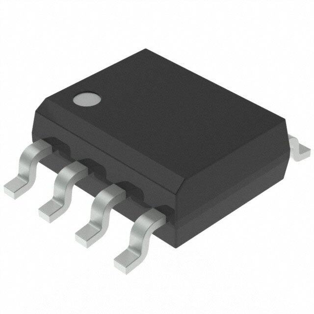
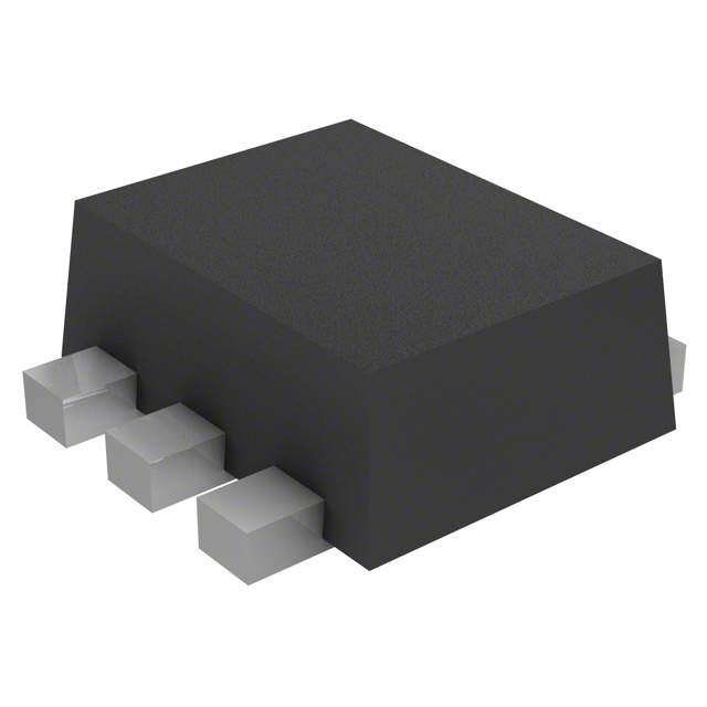
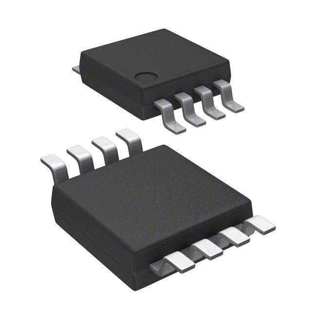
ICGOO在线商城 > 传感器,变送器 > 温度传感器 - 模拟和数字输出 > LM74CITP-3/NOPB
- 型号: LM74CITP-3/NOPB
- 制造商: Texas Instruments
- 库位|库存: xxxx|xxxx
- 要求:
| 数量阶梯 | 香港交货 | 国内含税 |
| +xxxx | $xxxx | ¥xxxx |
查看当月历史价格
查看今年历史价格
LM74CITP-3/NOPB产品简介:
ICGOO电子元器件商城为您提供LM74CITP-3/NOPB由Texas Instruments设计生产,在icgoo商城现货销售,并且可以通过原厂、代理商等渠道进行代购。 LM74CITP-3/NOPB价格参考¥8.40-¥18.99。Texas InstrumentsLM74CITP-3/NOPB封装/规格:温度传感器 - 模拟和数字输出, 温度传感器 数字,本地 -40°C ~ 125°C 12 b 5-DSBGA。您可以下载LM74CITP-3/NOPB参考资料、Datasheet数据手册功能说明书,资料中有LM74CITP-3/NOPB 详细功能的应用电路图电压和使用方法及教程。
| 参数 | 数值 |
| 产品目录 | |
| 描述 | IC TEMP SENSOR DGTL 5DSBGA板上安装温度传感器 SPI/ 12-Bit Plus Sign Temperature Sensor 5-DSBGA -40 to 125 |
| 产品分类 | 温度传感器,变送器温度传感器 |
| 品牌 | Texas Instruments |
| 产品手册 | |
| 产品图片 |
|
| rohs | 符合RoHS无铅 / 符合限制有害物质指令(RoHS)规范要求 |
| 产品系列 | 板上安装温度传感器,Texas Instruments LM74CITP-3/NOPB- |
| 数据手册 | |
| 产品型号 | LM74CITP-3/NOPB |
| 产品种类 | 板上安装温度传感器 |
| 供应商器件封装 | 5-DSBGA |
| 关闭 | Shutdown |
| 其它名称 | LM74CITP-3 |
| 准确性 | +/- 1.25 C, +/- 2.1 C, +/- 3 C |
| 包装 | 带卷 (TR) |
| 商标 | Texas Instruments |
| 安装风格 | SMD/SMT |
| 封装 | Reel |
| 封装/外壳 | 5-UFBGA,DSBGA |
| 封装/箱体 | DSBGA-5 |
| 工厂包装数量 | 250 |
| 感应温度 | -40°C ~ 125°C |
| 数字输出-位数 | 12 bit |
| 数字输出-总线接口 | 3-Wire, Microwire, SPI |
| 最大工作温度 | + 125 C |
| 最小工作温度 | - 40 C |
| 标准包装 | 250 |
| 电压-电源 | 2.65 V ~ 3.6 V |
| 电源电压-最大 | 5.5 V |
| 电源电压-最小 | 2.65 V |
| 电源电流 | 265 uA |
| 精度 | ±5°C(最大) |
| 系列 | LM74 |
| 设备功能 | Temperature Sensor |
| 输出类型 | Digital |
| 配置 | Local |


- 商务部:美国ITC正式对集成电路等产品启动337调查
- 曝三星4nm工艺存在良率问题 高通将骁龙8 Gen1或转产台积电
- 太阳诱电将投资9.5亿元在常州建新厂生产MLCC 预计2023年完工
- 英特尔发布欧洲新工厂建设计划 深化IDM 2.0 战略
- 台积电先进制程称霸业界 有大客户加持明年业绩稳了
- 达到5530亿美元!SIA预计今年全球半导体销售额将创下新高
- 英特尔拟将自动驾驶子公司Mobileye上市 估值或超500亿美元
- 三星加码芯片和SET,合并消费电子和移动部门,撤换高东真等 CEO
- 三星电子宣布重大人事变动 还合并消费电子和移动部门
- 海关总署:前11个月进口集成电路产品价值2.52万亿元 增长14.8%


PDF Datasheet 数据手册内容提取
LM74 www.ti.com SNIS107K–MAY2000–REVISEDMARCH2013 LM74 SPI/Microwire12-Bit Plus Sign Temperature Sensor CheckforSamples:LM74 FEATURES DESCRIPTION 1 • 0.0625°CTemperatureResolution The LM74 is a temperature sensor, Delta-Sigma 2 analog-to-digital converter with an SPI and • ShutdownModeConservesPowerBetween MICROWIRE compatible interface. The host can TemperatureReading query the LM74 at any time to read temperature. A • SPIandMICROWIREBusInterface shutdown mode decreases power consumption to • 5-BumpDSBGAPackageSavesSpace less than 10 μA. This mode is useful in systems wherelowaveragepowerconsumptioniscritical. APPLICATIONS The LM74 has 12-bit plus sign temperature resolution (0.0625°C per LSB) while operating over a • SystemThermalManagement temperaturerangeof−55°Cto+150°C. • PersonalComputers The LM74's 3.0V to 5.5V supply voltage range, low • DiskDrives supply current and simple SPI interface make it ideal • OfficeElectronics for a wide range of applications. These include • ElectronicTestEquipment thermal management and protection applications in hard disk drives, printers, electronic test equipment, KEY SPECIFICATIONS and office electronics. The LM74 is available in the SOIC package as well as the 5-Bump DSBGA • SupplyVoltage3.0Vor2.65Vto5.5V package. • SupplyCurrent BlockDiagram – Operating – 265μA(typ) – 520μA(max) – Shutdown – 3μA(typ) • TemperatureAccuracy – −10°Cto65°C,±1.25°C(max) – −25°Cto110°C,±2.1°C(max) – −55°Cto125°C,±3°C(max) Figure1. 1 Pleasebeawarethatanimportantnoticeconcerningavailability,standardwarranty,anduseincriticalapplicationsof TexasInstrumentssemiconductorproductsanddisclaimerstheretoappearsattheendofthisdatasheet. Alltrademarksarethepropertyoftheirrespectiveowners. 2 PRODUCTIONDATAinformationiscurrentasofpublicationdate. Copyright©2000–2013,TexasInstrumentsIncorporated Products conform to specifications per the terms of the Texas Instruments standard warranty. Production processing does not necessarilyincludetestingofallparameters.
LM74 SNIS107K–MAY2000–REVISEDMARCH2013 www.ti.com Connection Diagram GND (A3) (B3)CS SC (A2) SI/O (A1) (B1) V+ Figure2. SOIC– TopView Figure3.5-BumpDSBGA–TopView SeePackageNumberD SeePackageNumberYTA0005 PINDESCRIPTIONS SOIC DSBGA Label Function TypicalConnection Pin# Pin# SlaveInput/Output-Serialbusbi-directionaldataline. SI/O 1 1 FromandtoController Schmitttriggerinput. SlaveClock-SerialbusclockSchmitttriggerinput SC 2 5 FromController line. NC 3 NoConnection NoConnection GND 4 4 PowerSupplyGround Ground NC 5 NoConnection NoConnection NC 6 NoConnection NoConnection CS 7 3 ChipSelectinput. FromController DCVoltagefrom3.0Vto5.5VfortheLM74CIM V+ 8 2 PositiveSupplyVoltageInput and2.65Vto5.5VfortheLM74CIBPand LM74CITP.Bypasswitha0.1μFceramic capacitor. Typical Application +3.3 V L0(GPI/O) CS V+ 0.1 µF SI SI/O SK SC GND COP8SA Micro- Controller Figure4. COPMicrocontrollerInterface Thesedeviceshavelimitedbuilt-inESDprotection.Theleadsshouldbeshortedtogetherorthedeviceplacedinconductivefoam duringstorageorhandlingtopreventelectrostaticdamagetotheMOSgates. 2 SubmitDocumentationFeedback Copyright©2000–2013,TexasInstrumentsIncorporated ProductFolderLinks:LM74
LM74 www.ti.com SNIS107K–MAY2000–REVISEDMARCH2013 Absolute Maximum Ratings(1) SupplyVoltage −0.3Vto6.0V VoltageatanyPin −0.3VtoV++0.3V InputCurrentatanyPin(2) 5mA PackageInputCurrent(2) 20mA StorageTemperature −65°Cto+150°C ESDSusceptibility(3) HumanBodyModel LM74CIBPandLM74CITP,pinA2(SC) 1900V LM74CIM,LM74CIBP,andLM74CITPallotherpins 2000V MachineModel 200V SolderingprocessmustcomplywithReflowTemperatureProfilespecifications.Seewww.ti.com/packaging.(4) (1) AbsoluteMaximumRatingsindicatelimitsbeyondwhichdamagetothedevicemayoccur.DCandACelectricalspecificationsdonot applywhenoperatingthedevicebeyonditsratedoperatingconditions. (2) Whentheinputvoltage(V)atanypinexceedsthepowersupplies(V <GNDorV >+V )thecurrentatthatpinshouldbelimitedto5 I I I S mA.The20mAmaximumpackageinputcurrentratinglimitsthenumberofpinsthatcansafelyexceedthepowersupplieswithaninput currentof5mAtofour. (3) Humanbodymodel,100pFdischargedthrougha1.5kΩresistor.Machinemodel,200pFdischargeddirectlyintoeachpin. (4) Reflowtemperatureprofilesaredifferentforlead-freeandnon-lead-freepackages. Operating Ratings SpecifiedTemperatureRange T toT MIN MAX See(1) LM74CIBPandLM74CITP −40°Cto+125°C LM74CIM −55°Cto+150°C SupplyVoltageRange(+V ) S LM74CIBPandLM74CITP +2.65Vto+5.5V LM74CIM +3.0Vto+5.5V (1) ThelifeexpectancyoftheLM74willbereducedwhenoperatingatelevatedtemperatures.LM74θ (thermalresistance,junction-to- JA ambient)whenattachedtoaprintedcircuitboardwith2oz.foilissummarizedas:DeviceNumberLM74CIMThermalResistance(θ ) JA 160°C/W.DeviceNumberLM74CIBPThermalResistance(θ )250°C/W.DeviceNumberLM74CITPThermalResistance(θ ) JA JA 250°C/W. Copyright©2000–2013,TexasInstrumentsIncorporated SubmitDocumentationFeedback 3 ProductFolderLinks:LM74
LM74 SNIS107K–MAY2000–REVISEDMARCH2013 www.ti.com Temperature-to-Digital Converter Characteristics Unlessotherwisenoted,thesespecificationsapplyforV+=2.65Vto3.6VfortheLM74CIBP-3,LM74CITP-3,V+=3.0Vto 3.6VfortheLM74CIM-3andV+=4.5Vto5.5VfortheLM74-5(1).BoldfacelimitsapplyforT =T =T toT ;allother A J MIN MAX limitsT =T=+25°C,unlessotherwisenoted. A J Typical(2) LM74-5 LM74-3 Units Parameter Conditions Limits(3) Limits(3) (Limit) TemperatureError(1) T =−10°Cto+65°C ±1.25 ±1.25 °C(max) A T =−25°Cto+110°C ±2.1 +2.65/−2.15 °C(max) A T =−40°Cto+85°C +2.65/−1.65 ±2.15 °C(max) A T =−40°Cto+110°C +2.65/ +2.65/−2.15 °C(max) A −2.0 T =−55°Cto+125°C ±3.0 ±3.5 °C(max) A T =−55°Cto+150°C ±5.0 ±5.0 °C(max) A Resolution 13 Bits Temperature SOIC See(4) 280 425 425 ms(max) ConversionTime DSBGA See(4) 611 925 925 ms(max) QuiescentCurrent SOIC SerialBusInactive 310 520 520 μA(max) DSBGA 265 470 470 μA(max) SOIC SerialBusActive 310 μA DSBGA 310 μA SOIC ShutdownMode, 7 μA V+=3.3V DSBGA 3 μA SOIC ShutdownMode, 8 μA V+=5V DSBGA 4 μA (1) AllSOP(LM74CIM)partswillfunctionovertheV+supplyvoltagerangeof3Vto5.5V.AllDSBGA(LM74SIBPandLM75CITP)partswill functionovertheV+supplyvoltagerangeof2.65Vto5.5V.TheSOP(LM74CIM)partsaretestedandspecifiedforratedtemperature errorattheirnominalsupplyvoltagefortemperaturerangesof−10°Cto+65°C,−55°Cto+125°Cand−55°Cto+150°C.FortheSOP (LM74CIM)parts,thetemperatureerrorspecificationsfortemperaturerangesof−40°Cto+85°C,−25°Cto+110°C,and−40°Cto +110°Cincludeerrorinducedbypowersupplyvariationof±5%fromthenominalvalue.FortheLM74CIM(SOP)parts,thetemperature errorwillincreaseby±0.3°Cforapowersupplyvoltage(V+)variationof±10%fromthenominalvalue.FortheLM74CIBP-3and LM74CITP-3(DSBGA)partsallaccuraciesareensuredoverthesupplyrangeof2.65Vto3.6V,exceptforthetemperaturerangesof- 55°Cto125°Cand−55°Cto+150°Cwheretheaccuracyappliesforthenominalsupplyvoltageof3.3V.FortheLM74CIBP-5and LM74CITP-5(DSBGA)partsallaccuraciesareguranteedoverthesupplyrangeof4.75Vto5.25V,exceptforthetemperaturerangesof -55°Cto125°Cand−55°Cto+150°Cwheretheaccuracyappliesforthenominalsupplyvoltageof5.0V.FortheLM74CIBPand LM74CITPover-55°Cto125°Cand−55°Cto+150°C,apowersupplyvariationof±10%willdegradetheaccuracyby±0.3°C. (2) TypicalsareatT =25°Candrepresentmostlikelyparametricnorm. A (3) LimitsarespecifiedtoAOQL(AverageOutgoingQualityLevel). (4) Thisspecificationisprovidedonlytoindicatehowoftentemperaturedataisupdated.TheLM74canbereadatanytimewithoutregard toconversionstate(andwillyieldlastconversionresult).Aconversioninprogresswillnotbeinterrupted.Theoutputshiftregisterwillbe updatedatthecompletionofthereadandanewconversionrestarted. 4 SubmitDocumentationFeedback Copyright©2000–2013,TexasInstrumentsIncorporated ProductFolderLinks:LM74
LM74 www.ti.com SNIS107K–MAY2000–REVISEDMARCH2013 Logic Electrical Characteristics DIGITALDCCHARACTERISTICS Unlessotherwisenoted,thesespecificationsapplyforV+=2.65Vto3.6VfortheLM74CIBP-3,LM74CITP-3,V+=3.0Vto 3.6VfortheLM74CIM-3andV+=4.5Vto5.5VfortheLM74-5(1).BoldfacelimitsapplyforT =T =T toT ;allother A J MIN MAX limitsT =T=+25°C,unlessotherwisenoted. A J Typical(2) Limits(3) Units Symbol Parameter Conditions (Limit) V Logical“1”InputVoltage V+×0.7 V(min) IN(1) V++0.3 V(max) V Logical“0”InputVoltage −0.3 V(min) IN(0) V+×0.3 V(max) InputHysteresisVoltage V+=3.0Vto3.6V 0.8 0.35 V(min) V+=4.5Vto5.5V 0.8 0.33 V(min) I Logical“1”InputCurrent V =V+ 0.005 3.0 μA(max) IN(1) IN I Logical“0”InputCurrent V =0V −0.005 −3.0 μA(min) IN(0) IN C AllDigitalInputs 20 pF IN V HighLevelOutputVoltage I =−400μA 2.4 V(min) OH OH V LowLevelOutputVoltage I =+2mA 0.4 V(max) OL OL I TRI-STATEOutputLeakageCurrent V =GND −1 μA(min) O_TRI-STATE O V =V+ +1 μA O (max) (1) AllSOP(LM74CIM)partswillfunctionovertheV+supplyvoltagerangeof3Vto5.5V.AllDSBGA(LM74SIBPandLM75CITP)partswill functionovertheV+supplyvoltagerangeof2.65Vto5.5V.TheSOP(LM74CIM)partsaretestedandspecifiedforratedtemperature errorattheirnominalsupplyvoltagefortemperaturerangesof−10°Cto+65°C,−55°Cto+125°Cand−55°Cto+150°C.FortheSOP (LM74CIM)parts,thetemperatureerrorspecificationsfortemperaturerangesof−40°Cto+85°C,−25°Cto+110°C,and−40°Cto +110°Cincludeerrorinducedbypowersupplyvariationof±5%fromthenominalvalue.FortheLM74CIM(SOP)parts,thetemperature errorwillincreaseby±0.3°Cforapowersupplyvoltage(V+)variationof±10%fromthenominalvalue.FortheLM74CIBP-3and LM74CITP-3(DSBGA)partsallaccuraciesareensuredoverthesupplyrangeof2.65Vto3.6V,exceptforthetemperaturerangesof- 55°Cto125°Cand−55°Cto+150°Cwheretheaccuracyappliesforthenominalsupplyvoltageof3.3V.FortheLM74CIBP-5and LM74CITP-5(DSBGA)partsallaccuraciesareguranteedoverthesupplyrangeof4.75Vto5.25V,exceptforthetemperaturerangesof -55°Cto125°Cand−55°Cto+150°Cwheretheaccuracyappliesforthenominalsupplyvoltageof5.0V.FortheLM74CIBPand LM74CITPover-55°Cto125°Cand−55°Cto+150°C,apowersupplyvariationof±10%willdegradetheaccuracyby±0.3°C. (2) TypicalsareatT =25°Candrepresentmostlikelyparametricnorm. A (3) LimitsarespecifiedtoAOQL(AverageOutgoingQualityLevel). Copyright©2000–2013,TexasInstrumentsIncorporated SubmitDocumentationFeedback 5 ProductFolderLinks:LM74
LM74 SNIS107K–MAY2000–REVISEDMARCH2013 www.ti.com SERIALBUSDIGITALSWITCHINGCHARACTERISTICS Unlessotherwisenoted,thesespecificationsapplyforV+=2.65Vto3.6VfortheLM74CIBP-3,LM74CITP-3,V+=3.0Vto 3.6VfortheLM74CIM-3andV+=4.5Vto5.5VfortheLM74-5(1);C (loadcapacitance)onoutputlines=100pFunless L otherwisespecified.BoldfacelimitsapplyforT =T =T toT ;allotherlimitsT =T =+25°C,unlessotherwise A J MIN MAX A J noted. Typical(2) Limits(3) Units Symbol Parameter Conditions (Limit) t SC(Clock)Period 0.16 μs(min) 1 DC (max) t CSLowtoSC(Clock)HighSet-UpTime 100 ns(min) 2 t CSLowtoDataOut(SO)Delay 70 ns(max) 3 t SC(Clock)LowtoDataOut(SO)Delay 100 ns(max) 4 t CSHightoDataOut(SO)TRI-STATE 200 ns(max) 5 t SC(Clock)HightoDataIn(SI)HoldTime 50 ns(min) 6 t DataIn(SI)Set-UpTimetoSC(Clock)High 30 ns(min) 7 (1) AllSOP(LM74CIM)partswillfunctionovertheV+supplyvoltagerangeof3Vto5.5V.AllDSBGA(LM74SIBPandLM75CITP)partswill functionovertheV+supplyvoltagerangeof2.65Vto5.5V.TheSOP(LM74CIM)partsaretestedandspecifiedforratedtemperature errorattheirnominalsupplyvoltagefortemperaturerangesof−10°Cto+65°C,−55°Cto+125°Cand−55°Cto+150°C.FortheSOP (LM74CIM)parts,thetemperatureerrorspecificationsfortemperaturerangesof−40°Cto+85°C,−25°Cto+110°C,and−40°Cto +110°Cincludeerrorinducedbypowersupplyvariationof±5%fromthenominalvalue.FortheLM74CIM(SOP)parts,thetemperature errorwillincreaseby±0.3°Cforapowersupplyvoltage(V+)variationof±10%fromthenominalvalue.FortheLM74CIBP-3and LM74CITP-3(DSBGA)partsallaccuraciesareensuredoverthesupplyrangeof2.65Vto3.6V,exceptforthetemperaturerangesof- 55°Cto125°Cand−55°Cto+150°Cwheretheaccuracyappliesforthenominalsupplyvoltageof3.3V.FortheLM74CIBP-5and LM74CITP-5(DSBGA)partsallaccuraciesareguranteedoverthesupplyrangeof4.75Vto5.25V,exceptforthetemperaturerangesof -55°Cto125°Cand−55°Cto+150°Cwheretheaccuracyappliesforthenominalsupplyvoltageof5.0V.FortheLM74CIBPand LM74CITPover-55°Cto125°Cand−55°Cto+150°C,apowersupplyvariationof±10%willdegradetheaccuracyby±0.3°C. (2) TypicalsareatT =25°Candrepresentmostlikelyparametricnorm. A (3) LimitsarespecifiedtoAOQL(AverageOutgoingQualityLevel). Figure5. DataOutputTimingDiagram 6 SubmitDocumentationFeedback Copyright©2000–2013,TexasInstrumentsIncorporated ProductFolderLinks:LM74
LM74 www.ti.com SNIS107K–MAY2000–REVISEDMARCH2013 Figure6. TRI-STATEDataOutputTimingDiagram Figure7. DataInputTimingDiagram Copyright©2000–2013,TexasInstrumentsIncorporated SubmitDocumentationFeedback 7 ProductFolderLinks:LM74
LM74 SNIS107K–MAY2000–REVISEDMARCH2013 www.ti.com Electrical Characteristics 0,1001,0110,0000 Output Code +25°C +0.0625°C 0,0001,1001,0000 0,0000,0000,0001 Temperature 00,0000,0000,0000 0°C -55°C +150°C 1,1111,1111,1111 1,1110,0111,0000 -0.0625°C -25°C 1,1100,1001,0000 Figure8. Temperature-to-DigitalTransferFunction(Non-linearscaleforclarity) TRI-STATE Test Circuit Figure9. 8 SubmitDocumentationFeedback Copyright©2000–2013,TexasInstrumentsIncorporated ProductFolderLinks:LM74
LM74 www.ti.com SNIS107K–MAY2000–REVISEDMARCH2013 Typical Performance Characteristics AveragePower-OnResetVoltagevsTemperature StaticSupplyCurrentvsTemperature(SOIC) Figure10. Figure11. StaticSupplyCurrentvsTemperature(DSBGA) TemperatureError(SOIC) Figure12. Figure13. Copyright©2000–2013,TexasInstrumentsIncorporated SubmitDocumentationFeedback 9 ProductFolderLinks:LM74
LM74 SNIS107K–MAY2000–REVISEDMARCH2013 www.ti.com FUNCTIONAL DESCRIPTION The LM74 temperature sensor incorporates a band-gap type temperature sensor and 12-bit plus sign ΔΣ ADC (Delta-Sigma Analog-to-Digital Converter). Compatibility of the LM74's three wire serial interface with SPI and MICROWIRE allows simple communications with common microcontrollers and processors. Shutdown mode can be used to optimize current drain for different applications. A Manufacture's/Device ID register identifies the LM74asTexasInstrumentsproduct. Power Up and Power Down When the supply voltage is less than about 1.6V (typical), the LM74 is considered powered down. The LM74 always powers up in a known state. When the supply voltage rises above 1.6V (typical), an internal Power-On Reset (POR) occurs and the temperature register will then contain a value of 1111 1111 0000 00XX, where XX indicates undefined values. See Temperature Register (after power-up, before first complete temperature conversion)diagramforcontentsafterPORbutbeforecompletionofthefirsttemperatureconversion. The LM74 power-up default condition is continuous conversion mode. After completion of the first full temperature conversion, the register will contain temperature measurement data in bits D15 (the temperature data MSB) through D3 (the temperature data LSB). Bit D2 will be fixed high; bits D1 and D0 are undefined. See Section 1.5.3 for a diagram of the Temperature Regisiter contents after the first complete temperature conversion. Note that bit D2 represents a complete conversion flag. During POR it is low and, after the first temperature conversion is complete, it goes high. This bit can be polled to indicate when the POR data in the TemperatureRegisterhasbeenreplacedwithvalidtemperaturedata. After the first conversion, and any subsequent conversions, the value in the temperature register does not change until the completion of the next conversion, at which time the temperature register is updated with the latesttemperaturevalue. Serial Bus Interface The LM74 operates as a slave and is compatible with SPI or MICROWIRE bus specifications. Data is clocked out on the falling edge of the serial clock (SC), while data is clocked in on the rising edge of SC. A complete transmit/receivecommunicationwillconsistof32serialclocks.Thefirst16clockscomprisethetransmitphaseof communication,whilethesecond16clocksarethereceivephase. When CS is high SI/O will be in TRI-STATE. Communication should be initiated by taking chip select (CS) low. This should not be done when SC is changing from a low to high state. Once CS is low the serial I/O pin (SI/O) will transmit the first bit of data. The master can then read this bit with the rising edge of SC. The remainder of the data will be clocked out by the falling edge of SC. Once the 14 bits of data (one sign bit, twelve temperature bits and 1 high bit) are transmitted the SI/O line will go into TRI-STATE. CS can be taken high at any time during the transmit phase. If CS is brought low in the middle of a conversion the LM74 will complete the conversion and theoutputshiftregisterwillbeupdatedafterCSisbroughtbackhigh. The receive phase of a communication starts after 16 SC periods. CS can remain low for 32 SC cycles. The LM74 will read the data available on the SI/O line on the rising edge of the serial clock. Input data is to an 8-bit shift register. The part will detect the last eight bits shifted into the register. The receive phase can last up to 16 SC periods. All ones must be shifted in order to place the part into shutdown. A zero in any location will take the LM74outofshutdown.ThefollowingcodesshouldonlybetransmittedtotheLM74: • 00hex • 01hex • 03hex • 07hex • 0Fhex • 1Fhex • 3Fhex • 7Fhex • FFhex any others may place the part into a Test Mode. Test Modes are used by Texas Instruments to thoroughly test the function of the LM74 during production testing. Only eight bits have been defined above since only the last eighttransmittedaredetectedbytheLM74,beforeCSistakenHIGH. 10 SubmitDocumentationFeedback Copyright©2000–2013,TexasInstrumentsIncorporated ProductFolderLinks:LM74
LM74 www.ti.com SNIS107K–MAY2000–REVISEDMARCH2013 ThefollowingcommunicationcanbeusedtodeterminetheManufacturer's/DeviceIDandthenimmediatelyplace thepartintocontinuousconversionmode.WithCScontinuouslylow: • Read16bitsoftemperaturedata • Write16bitsofdatacommandingshutdown • Read16bitsofManufacture's/DeviceIDdata • Write8to16bitsofdatacommandingConversionMode • TakeCSHIGH. Note that one complete temperature conversion period will have to pass before the LM74 Temperature register will contain the new temperature data. Until then, it will contain a "stale" temperature (the data that was in the registerbeforegoingintoshutdownmode). Temperature Data Format Temperature data is represented by a 13-bit, two's complement word with an LSB (Least Significant Bit) equal to 0.0625°C: Temperature DigitalOutput Binary Hex +150°C 0100101100000111 4B07h +125°C 0011111010000111 3E87h +25°C 0000110010000111 0C87h +0.0625°C 0000000000001111 000Fh 0°C 0000000000000111 0007h −0.0625°C 1111111111111111 FFFFh −25°C 1111001110000111 F387h −55°C 1110010010000111 E487h Note:ThelasttwobitsareTRI-STATEanddepictedasoneinthetable. The first data byte is the most significant byte with most significant bit first, permitting only as much data as necessary to be read to determine temperature condition. For instance, if the first four bits of the temperature data indicate an overtemperature condition, the host processor could immediately take action to remedy the excessivetemperatures. Shutdown Mode/Manufacturer's ID Shutdown mode is enabled by writing XX FF to the LM74 as shown in Figure 16c. The serial bus is still active when the LM74 is in shutdown. Current draw drops to less than 10 μA between serial communications. When in shutdown mode the LM74 always will output 1000 0000 0000 00XX. This is the manufacturer's/Device ID information. The first 5-bits of the field (1000 0XXX) are reserved for manufacturer's ID. As mentioned in Section 1.2, writing a zero to the LM74 configuration register will take it out of shutdown mode and place it in conversion mode. In other words, any valid code listed in Section 1.2 other than XX FF will put it in conversion mode. After leaving shutdown, but before the first temperature conversion is complete, the temperature register will contain the last measured temperature which resided in the temperature register before entering shutdown mode. After thecompletionofthefirstconversion,thetemperatureregisterwillbeupdatedwiththenewtemperaturedata. Internal Register Structure The LM74 has three registers, the temperature register, the configuration register and the manufacturer's/device identification register. The temperature and manufacturer's/device identification registers are read only. The configurationregisteriswriteonly. ConfigurationRegister (Selectsshutdownorcontinuousconversionmodes): Copyright©2000–2013,TexasInstrumentsIncorporated SubmitDocumentationFeedback 11 ProductFolderLinks:LM74
LM74 SNIS107K–MAY2000–REVISEDMARCH2013 www.ti.com Table1.(WriteOnly): D15 D14 D13 D12 D11 D10 D9 D8 D7 D6 D5 D4 D3 D2 D1 D0 X X X X X X X X Shutdown D0–D15settoXXFFhexenablesshutdownmode. D0–D15setto0000hexsetsContinuousconversionmode. Note: setting D0-D15 to any other values may place the LM74 into a manufacturer's test mode, upon which the LM74 will stop responding as described. These test modes are to be used for Texas Instruments production testingonly.SeeSerialBusInterfaceforacompletediscussion. TemperatureRegister(afterpower-up,beforefirstcompletetemperatureconversion) Table2.(ReadOnly): D15 D14 D13 D12 D11 D10 D9 D8 D7 D6 D5 D4 D3 D2 D1 D0 1 1 1 1 1 1 1 1 0 0 0 0 0 0 X X D0–D1:Undefined.TRI-STATEwillbeoutputonSI/0. D2–D15:Power-onReset(POR)values. TemperatureRegister(aftercompletionoffirsttemperatureconversion) Table3.(ReadOnly): D15 D14 D13 D12 D11 D10 D9 D8 D7 D6 D5 D4 D3 D2 D1 D0 MSB Bit11 Bit10 Bit9 Bit8 Bit7 Bit6 Bit5 Bit4 Bit3 Bit2 Bit1 LSB 1 X X D0–D1:Undefined.TRI-STATEwillbeoutputonSI/0. D2:High. D3–D15:TemperatureData.OneLSB=0.0625°C.Two'scomplementformat. Manufacturer'sDeviceIDRegister Table4.(ReadOnly): D15 D14 D13 D12 D11 D10 D9 D8 D7 D6 D5 D4 D3 D2 D1 D0 1 0 0 0 0 0 0 0 0 0 0 0 0 0 X X D0–D1:Undefined.TRI-STATEwillbeoutputonSI/0. D2–D15:Manufacturer's/DeviceIDData.ThisregisterisaccessedwhenevertheLM74isinshutdownmode. 12 SubmitDocumentationFeedback Copyright©2000–2013,TexasInstrumentsIncorporated ProductFolderLinks:LM74
LM74 www.ti.com SNIS107K–MAY2000–REVISEDMARCH2013 Serial Bus Timing Diagrams Figure14. a)ReadingContinuousConversion-SingleEight-BitFrame Figure15. b)ReadingContinuousConversion-TwoEight-BitFrames Figure16. c)WritingShutdownControl ApplicationHints To get the expected results when measuring temperature with an integrated circuit temperature sensor like the LM74, it is important to understand that the sensor measures its own die temperature. For the LM74, the best thermal path between the die and the outside world is through the LM74's pins. In the SOIC package all the pins ontheLM74willhaveanequaleffectonthedietemperature.Becausethepinsrepresentagoodthermalpathto the LM74 die, the LM74 will provide an accurate measurement of the temperature of the printed circuit board on which it is mounted. There is a less efficient thermal path between the plastic package and the LM74 die. If the ambient air temperature is significantly different from the printed circuit board temperature, it will have a small effectonthemeasuredtemperature. In probe-type applications, the LM74 can be mounted inside a sealed-end metal tube, and can then be dipped into a bath or screwed into a threaded hole in a tank. As with any IC, the LM74 and accompanying wiring and circuits must be kept insulated and dry, to avoid leakage and corrosion. This is especially true if the circuit may operate at cold temperatures where condensation can occur. Printed-circuit coatings and varnishes such as Humiseal and epoxy paints or dips are often used to insure that moisture cannot corrode the LM74 or its connections. DSBGALightSensitivity The LM74 in the DSBGA package should not be exposed to ultraviolet light. The DSBGA package does not completely encapsulate the LM74 die in epoxy. Exposing the LM74 DSBGA package to bright sunlight will not immediatly cause a change in the output reading. Our experiments show that directly exposing the circuit side (bump side) of the die to high intensity (≥ 1mW/cm2) ultraviolet light, centered at a wavelength of 254nm, for greater than 20 minutes will deprogram the EEPROM cells in the LM74. Since the EEPROM is used for storing calibration coefficients, the LM74 will function but the temperature accuracy will no longer be as specified. Light can penetrate through the side of the package as well, so exposure to ultra violet radiation is not recommended evenaftermounting. Copyright©2000–2013,TexasInstrumentsIncorporated SubmitDocumentationFeedback 13 ProductFolderLinks:LM74
LM74 SNIS107K–MAY2000–REVISEDMARCH2013 www.ti.com Typical Applications Figure17. TemperaturemonitorusingIntel196processor Figure18. LM74digitalinputcontrolusingmicrocontroller'sgeneralpurposeI/O. 14 SubmitDocumentationFeedback Copyright©2000–2013,TexasInstrumentsIncorporated ProductFolderLinks:LM74
LM74 www.ti.com SNIS107K–MAY2000–REVISEDMARCH2013 REVISION HISTORY ChangesfromRevisionJ(March2013)toRevisionK Page • ChangedlayoutofNationalDataSheettoTIformat.......................................................................................................... 14 Copyright©2000–2013,TexasInstrumentsIncorporated SubmitDocumentationFeedback 15 ProductFolderLinks:LM74
PACKAGE OPTION ADDENDUM www.ti.com 23-Sep-2017 PACKAGING INFORMATION Orderable Device Status Package Type Package Pins Package Eco Plan Lead/Ball Finish MSL Peak Temp Op Temp (°C) Device Marking Samples (1) Drawing Qty (2) (6) (3) (4/5) LM74CIM-3 NRND SOIC D 8 95 TBD Call TI Call TI -55 to 150 LM74 CIM3 LM74CIM-3/NOPB ACTIVE SOIC D 8 95 Green (RoHS CU SN Level-1-260C-UNLIM -55 to 150 LM74 & no Sb/Br) CIM3 LM74CIM-5 NRND SOIC D 8 95 TBD Call TI Call TI -55 to 150 LM74 CIM5 LM74CIM-5/NOPB ACTIVE SOIC D 8 95 Green (RoHS CU SN Level-1-260C-UNLIM -55 to 150 LM74 & no Sb/Br) CIM5 LM74CIMX-3 NRND SOIC D 8 2500 TBD Call TI Call TI -55 to 150 LM74 CIM3 LM74CIMX-3/NOPB ACTIVE SOIC D 8 2500 Green (RoHS CU SN Level-1-260C-UNLIM -55 to 150 LM74 & no Sb/Br) CIM3 LM74CIMX-5/NOPB ACTIVE SOIC D 8 2500 Green (RoHS CU SN Level-1-260C-UNLIM -55 to 150 LM74 & no Sb/Br) CIM5 LM74CITP-3/NOPB ACTIVE DSBGA YTA 5 250 Green (RoHS SNAGCU Level-1-260C-UNLIM -40 to 125 10 & no Sb/Br) LM74CITPX-3/NOPB ACTIVE DSBGA YTA 5 3000 Green (RoHS SNAGCU Level-1-260C-UNLIM -40 to 125 10 & no Sb/Br) (1) The marketing status values are defined as follows: ACTIVE: Product device recommended for new designs. LIFEBUY: TI has announced that the device will be discontinued, and a lifetime-buy period is in effect. NRND: Not recommended for new designs. Device is in production to support existing customers, but TI does not recommend using this part in a new design. PREVIEW: Device has been announced but is not in production. Samples may or may not be available. OBSOLETE: TI has discontinued the production of the device. (2) RoHS: TI defines "RoHS" to mean semiconductor products that are compliant with the current EU RoHS requirements for all 10 RoHS substances, including the requirement that RoHS substance do not exceed 0.1% by weight in homogeneous materials. Where designed to be soldered at high temperatures, "RoHS" products are suitable for use in specified lead-free processes. TI may reference these types of products as "Pb-Free". RoHS Exempt: TI defines "RoHS Exempt" to mean products that contain lead but are compliant with EU RoHS pursuant to a specific EU RoHS exemption. Green: TI defines "Green" to mean the content of Chlorine (Cl) and Bromine (Br) based flame retardants meet JS709B low halogen requirements of <=1000ppm threshold. Antimony trioxide based flame retardants must also meet the <=1000ppm threshold requirement. (3) MSL, Peak Temp. - The Moisture Sensitivity Level rating according to the JEDEC industry standard classifications, and peak solder temperature. Addendum-Page 1
PACKAGE OPTION ADDENDUM www.ti.com 23-Sep-2017 (4) There may be additional marking, which relates to the logo, the lot trace code information, or the environmental category on the device. (5) Multiple Device Markings will be inside parentheses. Only one Device Marking contained in parentheses and separated by a "~" will appear on a device. If a line is indented then it is a continuation of the previous line and the two combined represent the entire Device Marking for that device. (6) Lead/Ball Finish - Orderable Devices may have multiple material finish options. Finish options are separated by a vertical ruled line. Lead/Ball Finish values may wrap to two lines if the finish value exceeds the maximum column width. Important Information and Disclaimer:The information provided on this page represents TI's knowledge and belief as of the date that it is provided. TI bases its knowledge and belief on information provided by third parties, and makes no representation or warranty as to the accuracy of such information. Efforts are underway to better integrate information from third parties. TI has taken and continues to take reasonable steps to provide representative and accurate information but may not have conducted destructive testing or chemical analysis on incoming materials and chemicals. TI and TI suppliers consider certain information to be proprietary, and thus CAS numbers and other limited information may not be available for release. In no event shall TI's liability arising out of such information exceed the total purchase price of the TI part(s) at issue in this document sold by TI to Customer on an annual basis. Addendum-Page 2
PACKAGE MATERIALS INFORMATION www.ti.com 24-Aug-2017 TAPE AND REEL INFORMATION *Alldimensionsarenominal Device Package Package Pins SPQ Reel Reel A0 B0 K0 P1 W Pin1 Type Drawing Diameter Width (mm) (mm) (mm) (mm) (mm) Quadrant (mm) W1(mm) LM74CIMX-3 SOIC D 8 2500 330.0 12.4 6.5 5.4 2.0 8.0 12.0 Q1 LM74CIMX-3/NOPB SOIC D 8 2500 330.0 12.4 6.5 5.4 2.0 8.0 12.0 Q1 LM74CIMX-5/NOPB SOIC D 8 2500 330.0 12.4 6.5 5.4 2.0 8.0 12.0 Q1 LM74CITP-3/NOPB DSBGA YTA 5 250 178.0 8.4 1.7 1.7 0.76 4.0 8.0 Q1 LM74CITPX-3/NOPB DSBGA YTA 5 3000 178.0 8.4 1.7 1.7 0.76 4.0 8.0 Q1 PackMaterials-Page1
PACKAGE MATERIALS INFORMATION www.ti.com 24-Aug-2017 *Alldimensionsarenominal Device PackageType PackageDrawing Pins SPQ Length(mm) Width(mm) Height(mm) LM74CIMX-3 SOIC D 8 2500 367.0 367.0 35.0 LM74CIMX-3/NOPB SOIC D 8 2500 367.0 367.0 35.0 LM74CIMX-5/NOPB SOIC D 8 2500 367.0 367.0 35.0 LM74CITP-3/NOPB DSBGA YTA 5 250 210.0 185.0 35.0 LM74CITPX-3/NOPB DSBGA YTA 5 3000 210.0 185.0 35.0 PackMaterials-Page2
PACKAGE OUTLINE D0008A SOIC - 1.75 mm max height SCALE 2.800 SMALL OUTLINE INTEGRATED CIRCUIT C SEATING PLANE .228-.244 TYP [5.80-6.19] .004 [0.1] C A PIN 1 ID AREA 6X .050 [1.27] 8 1 2X .189-.197 [4.81-5.00] .150 NOTE 3 [3.81] 4X (0 -15 ) 4 5 8X .012-.020 B .150-.157 [0.31-0.51] .069 MAX [3.81-3.98] .010 [0.25] C A B [1.75] NOTE 4 .005-.010 TYP [0.13-0.25] 4X (0 -15 ) SEE DETAIL A .010 [0.25] .004-.010 0 - 8 [0.11-0.25] .016-.050 [0.41-1.27] DETAIL A (.041) TYPICAL [1.04] 4214825/C 02/2019 NOTES: 1. Linear dimensions are in inches [millimeters]. Dimensions in parenthesis are for reference only. Controlling dimensions are in inches. Dimensioning and tolerancing per ASME Y14.5M. 2. This drawing is subject to change without notice. 3. This dimension does not include mold flash, protrusions, or gate burrs. Mold flash, protrusions, or gate burrs shall not exceed .006 [0.15] per side. 4. This dimension does not include interlead flash. 5. Reference JEDEC registration MS-012, variation AA. www.ti.com
EXAMPLE BOARD LAYOUT D0008A SOIC - 1.75 mm max height SMALL OUTLINE INTEGRATED CIRCUIT 8X (.061 ) [1.55] SYMM SEE DETAILS 1 8 8X (.024) [0.6] SYMM (R.002 ) TYP [0.05] 5 4 6X (.050 ) [1.27] (.213) [5.4] LAND PATTERN EXAMPLE EXPOSED METAL SHOWN SCALE:8X SOLDER MASK SOLDER MASK METAL OPENING OPENING METAL UNDER SOLDER MASK EXPOSED METAL EXPOSED METAL .0028 MAX .0028 MIN [0.07] [0.07] ALL AROUND ALL AROUND NON SOLDER MASK SOLDER MASK DEFINED DEFINED SOLDER MASK DETAILS 4214825/C 02/2019 NOTES: (continued) 6. Publication IPC-7351 may have alternate designs. 7. Solder mask tolerances between and around signal pads can vary based on board fabrication site. www.ti.com
EXAMPLE STENCIL DESIGN D0008A SOIC - 1.75 mm max height SMALL OUTLINE INTEGRATED CIRCUIT 8X (.061 ) [1.55] SYMM 1 8 8X (.024) [0.6] SYMM (R.002 ) TYP [0.05] 5 4 6X (.050 ) [1.27] (.213) [5.4] SOLDER PASTE EXAMPLE BASED ON .005 INCH [0.125 MM] THICK STENCIL SCALE:8X 4214825/C 02/2019 NOTES: (continued) 8. Laser cutting apertures with trapezoidal walls and rounded corners may offer better paste release. IPC-7525 may have alternate design recommendations. 9. Board assembly site may have different recommendations for stencil design. www.ti.com
MECHANICAL DATA YTA0005xxx 0.500±0.075 D E TPD05XXX (Rev A) D: Max = 1.667 mm, Min =1 .606 mm E: Max = 1.616 mm, Min =1 .555 mm 4215103/A 12/12 NOTES: A. All linear dimensions are in millimeters. Dimensioning and tolerancing per ASME Y14.5M-1994. B. This drawing is subject to change without notice. www.ti.com
IMPORTANTNOTICEANDDISCLAIMER TIPROVIDESTECHNICALANDRELIABILITYDATA(INCLUDINGDATASHEETS),DESIGNRESOURCES(INCLUDINGREFERENCE DESIGNS),APPLICATIONOROTHERDESIGNADVICE,WEBTOOLS,SAFETYINFORMATION,ANDOTHERRESOURCES“ASIS” ANDWITHALLFAULTS,ANDDISCLAIMSALLWARRANTIES,EXPRESSANDIMPLIED,INCLUDINGWITHOUTLIMITATIONANY IMPLIEDWARRANTIESOFMERCHANTABILITY,FITNESSFORAPARTICULARPURPOSEORNON-INFRINGEMENTOFTHIRD PARTYINTELLECTUALPROPERTYRIGHTS. TheseresourcesareintendedforskilleddevelopersdesigningwithTIproducts.Youaresolelyresponsiblefor(1)selectingtheappropriate TIproductsforyourapplication,(2)designing,validatingandtestingyourapplication,and(3)ensuringyourapplicationmeetsapplicable standards,andanyothersafety,security,orotherrequirements.Theseresourcesaresubjecttochangewithoutnotice.TIgrantsyou permissiontousetheseresourcesonlyfordevelopmentofanapplicationthatusestheTIproductsdescribedintheresource.Other reproductionanddisplayoftheseresourcesisprohibited.NolicenseisgrantedtoanyotherTIintellectualpropertyrightortoanythird partyintellectualpropertyright.TIdisclaimsresponsibilityfor,andyouwillfullyindemnifyTIanditsrepresentativesagainst,anyclaims, damages,costs,losses,andliabilitiesarisingoutofyouruseoftheseresources. TI’sproductsareprovidedsubjecttoTI’sTermsofSale(www.ti.com/legal/termsofsale.html)orotherapplicabletermsavailableeitheron ti.comorprovidedinconjunctionwithsuchTIproducts.TI’sprovisionoftheseresourcesdoesnotexpandorotherwisealterTI’sapplicable warrantiesorwarrantydisclaimersforTIproducts. MailingAddress:TexasInstruments,PostOfficeBox655303,Dallas,Texas75265 Copyright©2019,TexasInstrumentsIncorporated

 Datasheet下载


