ICGOO在线商城 > 传感器,变送器 > 温度传感器 - 模拟和数字输出 > LM56BIMM/NOPB

 Datasheet下载
- 型号: LM56BIMM/NOPB
- 制造商: Texas Instruments
- 库位|库存: xxxx|xxxx
- 要求:
| 数量阶梯 | 香港交货 | 国内含税 |
| +xxxx | $xxxx | ¥xxxx |
查看当月历史价格
查看今年历史价格
LM56BIMM/NOPB产品简介:
ICGOO电子元器件商城为您提供LM56BIMM/NOPB由Texas Instruments设计生产,在icgoo商城现货销售,并且可以通过原厂、代理商等渠道进行代购。 LM56BIMM/NOPB价格参考¥8.45-¥19.11。Texas InstrumentsLM56BIMM/NOPB封装/规格:温度传感器 - 模拟和数字输出, 温度传感器 模拟,本地 -40°C ~ 125°C 6.2mV/°C 8-VSSOP。您可以下载LM56BIMM/NOPB参考资料、Datasheet数据手册功能说明书,资料中有LM56BIMM/NOPB 详细功能的应用电路图电压和使用方法及教程。
| 参数 | 数值 |
| 产品目录 | |
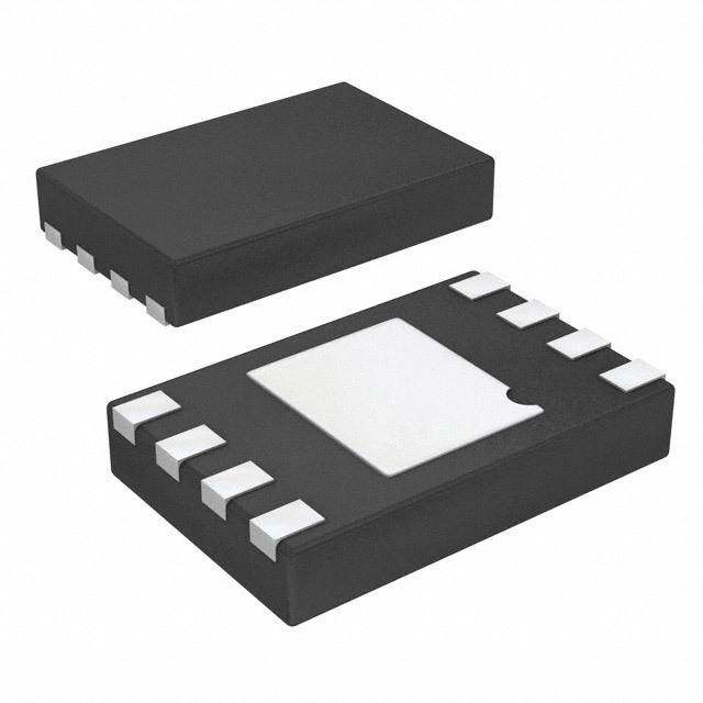
| 描述 | IC THERMOSTAT DUAL LO PWR 8VSSOP恒温器 Dual Output Lo Pwr Thermostat |
| 产品分类 | 温度传感器,变送器温度传感器 |
| 品牌 | Texas Instruments |
| 产品手册 | |
| 产品图片 |
|
| rohs | 符合RoHS无铅 / 符合限制有害物质指令(RoHS)规范要求 |
| 产品系列 | 恒温器,Texas Instruments LM56BIMM/NOPBPowerWise® |
| 数据手册 | |
| 产品型号 | LM56BIMM/NOPB |
| 产品 | Digital Thermostats |
| 产品目录页面 | |
| 产品种类 | 恒温器 |
| 供应商器件封装 | 8-VSSOP |
| 其它名称 | LM56BIMM/NOPBDKR |
| 准确性 | 2 C |
| 制造商产品页 | http://www.ti.com/general/docs/suppproductinfo.tsp?distId=10&orderablePartNumber=LM56BIMM/NOPB |
| 包装 | Digi-Reel® |
| 商标 | Texas Instruments |
| 封装 | Reel |
| 封装/外壳 | 8-TSSOP,8-MSOP(0.118",3.00mm 宽) |
| 工厂包装数量 | 1000 |
| 感应温度 | -40°C ~ 125°C |
| 标准包装 | 1 |
| 温度范围 | - 40 C to + 125 C |
| 电压-电源 | 2.7 V ~ 10 V |
| 电压额定值 | 10 V |
| 电流额定值 | 230 uA |
| 精度 | ±2°C |
| 系列 | LM56 |
| 输出类型 | 数字,开路集电极 |


- 商务部:美国ITC正式对集成电路等产品启动337调查
- 曝三星4nm工艺存在良率问题 高通将骁龙8 Gen1或转产台积电
- 太阳诱电将投资9.5亿元在常州建新厂生产MLCC 预计2023年完工
- 英特尔发布欧洲新工厂建设计划 深化IDM 2.0 战略
- 台积电先进制程称霸业界 有大客户加持明年业绩稳了
- 达到5530亿美元!SIA预计今年全球半导体销售额将创下新高
- 英特尔拟将自动驾驶子公司Mobileye上市 估值或超500亿美元
- 三星加码芯片和SET,合并消费电子和移动部门,撤换高东真等 CEO
- 三星电子宣布重大人事变动 还合并消费电子和移动部门
- 海关总署:前11个月进口集成电路产品价值2.52万亿元 增长14.8%


PDF Datasheet 数据手册内容提取
LM56 www.ti.com SNIS120G–APRIL2000–REVISEDFEBRUARY2013 LM56 Dual Output Low Power Thermostat CheckforSamples:LM56 FEATURES DESCRIPTION 1 • DigitalOutputsSupportTTLLogicLevels The LM56 is a precision low power thermostat. Two 2 stable temperature trip points (V and V ) are • InternalTemperatureSensor T1 T2 generated by dividing down the LM56 1.250V • 2InternalComparatorswithHysteresis bandgap voltage reference using 3 external resistors. • InternalVoltageReference The LM56 has two digital outputs. OUT1 goes LOW when the temperature exceeds T1 and goes HIGH • Availablein8-pinSOICandVSSOPPackages when the the temperature goes below (T1–T ). HYST Similarly, OUT2 goes LOW when the temperature APPLICATIONS exceeds T2 and goes HIGH when the temperature • MicroprocessorThermalManagement goes below (T2–THYST). THYST is an internally set 5°C typicalhysteresis. • Appliances • PortableBatteryPowered3.0Vor5VSystems The LM56 is available in an 8-lead VSSOP surface mountpackageandan8-leadSOIC. • FanControl • IndustrialProcessControl • HVACSystems • RemoteTemperatureSensing • ElectronicSystemProtection Table1.KeySpecifications VALUE UNIT PowerSupplyVoltage 2.7V–10 V PowerSupplyCurrent 230 μA(max) V 1.250 V±1%(max) REF HysteresisTemperature 5 °C (+6.20mV/°CxT)+ InternalTemperatureSensorOutputVoltage mV 395mV Table2.TemperatureTripPointAccuracy LM56BIM LM56CIM +25°C ±2°C(max) ±3°C(max) +25°Cto+85°C ±2°C(max) ±3°C(max) −40°Cto+125°C ±3°C(max) ±4°C(max) 1 Pleasebeawarethatanimportantnoticeconcerningavailability,standardwarranty,anduseincriticalapplicationsof TexasInstrumentssemiconductorproductsanddisclaimerstheretoappearsattheendofthisdatasheet. Alltrademarksarethepropertyoftheirrespectiveowners. 2 PRODUCTIONDATAinformationiscurrentasofpublicationdate. Copyright©2000–2013,TexasInstrumentsIncorporated Products conform to specifications per the terms of the Texas Instruments standard warranty. Production processing does not necessarilyincludetestingofallparameters.
LM56 SNIS120G–APRIL2000–REVISEDFEBRUARY2013 www.ti.com Simplified Block Diagram and Connection Diagram BlockDiagram Typical Application V =1.250Vx(R1)/(R1+R2+R3) T1 V =1.250Vx(R1+R2)/(R1+R2+R3) T2 where: (R1+R2+R3)=27kΩand V =[6.20mV/°CxT]+395mVtherefore: T1orT2 R1=V /(1.25V)x27kΩ T1 R2=(V /(1.25V)x27kΩ)−R1 T2 R3=27kΩ−R1−R2 Figure1. MicroprocessorThermalManagement Thesedeviceshavelimitedbuilt-inESDprotection.Theleadsshouldbeshortedtogetherorthedeviceplacedinconductivefoam duringstorageorhandlingtopreventelectrostaticdamagetotheMOSgates. 2 SubmitDocumentationFeedback Copyright©2000–2013,TexasInstrumentsIncorporated ProductFolderLinks:LM56
LM56 www.ti.com SNIS120G–APRIL2000–REVISEDFEBRUARY2013 Absolute Maximum Ratings(1) InputVoltage 12V InputCurrentatanypin(2) 5mA PackageInputCurrent(2) 20mA PackageDissipationatT =25°C(3) 900mW A HumanBodyModel-Pin3Only 800V Allotherpins 1000V ESDSusceptibility(4) MachineModel 125V StorageTemperature −65°Cto+150°C (1) AbsoluteMaximumRatingsindicatelimitsbeyondwhichdamagetothedevicemayoccur.OperatingRatingsindicateconditionsfor whichthedeviceisfunctional,butdonotguaranteespecificperformancelimits.Forguaranteedspecificationsandtestconditions,see theLM56ElectricalCharacteristics.Theguaranteedspecificationsapplyonlyforthetestconditionslisted.Someperformance characteristicsmaydegradewhenthedeviceisnotoperatedunderthelistedtestconditions. (2) Whentheinputvoltage(V)atanypinexceedsthepowersupply(V <GNDorV >V+),thecurrentatthatpinshouldbelimitedto5mA. I I I The20mAmaximumpackageinputcurrentratinglimitsthenumberofpinsthatcansafelyexceedthepowersupplieswithaninput currentof5mAtofour. (3) ThemaximumpowerdissipationmustbederatedatelevatedtemperaturesandisdictatedbyT (maximumjunctiontemperature), Jmax θ (junctiontoambientthermalresistance)andT (ambienttemperature).Themaximumallowablepowerdissipationatany JA A temperatureisP =(T –T )/θ orthenumbergivenintheAbsoluteMaximumRatings,whicheverislower.Forthisdevice,T = D Jmax A JA Jmax 125°C.Forthisdevicethetypicalthermalresistance(θ )ofthedifferentpackagetypeswhenboardmountedfollow: JA (4) Thehumanbodymodelisa100pFcapacitordischargethrougha1.5kΩresistorintoeachpin.Themachinemodelisa200pF capacitordischargeddirectlyintoeachpin. Operating Ratings(1)(2)(3) OperatingTemperatureRange T ≤T ≤T MIN A MAX LM56BIM,LM56CIM −40°C≤T ≤+125°C A PositiveSupplyVoltage(V+) +2.7Vto+10V MaximumV andV +10V OUT1 OUT2 (1) AbsoluteMaximumRatingsindicatelimitsbeyondwhichdamagetothedevicemayoccur.OperatingRatingsindicateconditionsfor whichthedeviceisfunctional,butdonotguaranteespecificperformancelimits.Forguaranteedspecificationsandtestconditions,see theLM56ElectricalCharacteristics.Theguaranteedspecificationsapplyonlyforthetestconditionslisted.Someperformance characteristicsmaydegradewhenthedeviceisnotoperatedunderthelistedtestconditions. (2) SolderingprocessmustcomplywithReflowTemperatureProfilespecifications.Refertohttp://www.ti.com/packaging. (3) Reflowtemperatureprofilesaredifferentforlead-freeandnon-lead-freepackages. PackageType θ JA D0008A 110°C/W DGK0008A 250°C/W Copyright©2000–2013,TexasInstrumentsIncorporated SubmitDocumentationFeedback 3 ProductFolderLinks:LM56
LM56 SNIS120G–APRIL2000–REVISEDFEBRUARY2013 www.ti.com LM56 Electrical Characteristics ThefollowingspecificationsapplyforV+=2.7V ,andV loadcurrent=50μAunlessotherwisespecified.Boldfacelimits DC REF applyforT =T =T toT ;allotherlimitsT =T =25°Cunlessotherwisespecified. A J MIN MAX A J Symbol Parameter Conditions Typical(1) LLMim56itBs(I2M) LLMim56itCs(I2M) Units(Limits) TemperatureSensor TripPointAccuracy(IncludesV , ±2 ±3 °C(max) REF ComparatorOffset,andTemperature +25°C≤T ≤+85°C ±2 ±3 °C(max) Sensitivityerrors) A −40°C≤T ≤+125°C ±3 ±4 °C(max) A TripPointHysteresis T =−40°C 4 3 3 °C(min) A 6 6 °C(max) T =+25°C 5 3.5 3.5 °C(min) A 6.5 6.5 °C(max) T =+85°C 6 4.5 4.5 °C(min) A 7.5 7.5 °C(max) T =+125°C 6 4 4 °C(min) A 8 8 °C(max) InternalTemperatureSensitivity +6.20 mV/°C TemperatureSensitivityError ±2 ±3 °C(max) ±3 ±4 °C(max) OutputImpedance −1μA≤I ≤+40μA 1500 1500 Ω(max) L LineRegulation +3.0V≤V+≤+10V, –0.72/+0.3 –0.72/+0.3 mV/V(max) +25°C≤T ≤+85°C 6 6 A +3.0V≤V+≤+10V, –1.14/+0.6 –1.14/+0.6 mV/V(max) −40°C≤T <25°C 1 1 A +2.7V≤V+≤+3.3V ±2.3 ±2.3 mV(max) V andV AnalogInputs T1 T2 I AnalogInputBiasCurrent 150 300 300 nA(max) BIAS V AnalogInputVoltageRange V+−1 V IN GND V V ComparatorOffset 2 8 8 mV(max) OS V Output REF V V Nominal 1.250V V REF REF V Error ±1 ±1 %(max) REF ±12.5 ±12.5 mV(max) ΔV /ΔV+ LineRegulation +3.0V≤V+≤+10V 0.13 0.25 0.25 mV/V(max) REF +2.7V≤V+≤+3.3V 0.15 1.1 1.1 mV(max) ΔV /ΔI LoadRegulationSourcing +30μA≤I ≤+50μA 0.15 0.15 mV/μA(max) REF L L (1) TypicalsareatT =T =25°Candrepresentmostlikelyparametricnorm. J A (2) LimitsareguaranteedtoTI'sAOQL(AverageOutgoingQualityLevel). Symbol Parameter Conditions Typical(1) Limits(2) Units(Limits) V+PowerSupply I SupplyCurrent V+=+10V 230 μA(max) S V+=+2.7V 230 μA(max) DigitalOutputs I Logical“1”OutputLeakageCurrent V+=+5.0V 1 μA(max) OUT(“1”) V Logical“0”OutputVoltage I =+50μA 0.4 V(max) OUT(“0”) OUT (1) TypicalsareatT =T =25°Candrepresentmostlikelyparametricnorm. J A (2) LimitsareguaranteedtoTI'sAOQL(AverageOutgoingQualityLevel). 4 SubmitDocumentationFeedback Copyright©2000–2013,TexasInstrumentsIncorporated ProductFolderLinks:LM56
LM56 www.ti.com SNIS120G–APRIL2000–REVISEDFEBRUARY2013 Typical Performance Characteristics QuiescentCurrent V OutputVoltage REF vs vs Temperature LoadCurrent Figure2. Figure3. OUT1andOUT2VoltageLevels TripPointHysteresis vs vs LoadCurrent Temperature Figure4. Figure5. TemperatureSensorOutputVoltage TemperatureSensorOutputAccuracy vs vs Temperature Temperature Figure6. Figure7. Copyright©2000–2013,TexasInstrumentsIncorporated SubmitDocumentationFeedback 5 ProductFolderLinks:LM56
LM56 SNIS120G–APRIL2000–REVISEDFEBRUARY2013 www.ti.com Typical Performance Characteristics (continued) TripPointAccuracy ComparatorBiasCurrent vs vs Temperature Temperature Figure8. Figure9. OUT1andOUT2LeakageCurrent V OutputLineRegulation TEMP vs vs Temperature Temperature Figure10. Figure11. V Start-UpResponse V Start-UpResponse REF TEMP Figure12. Figure13. 6 SubmitDocumentationFeedback Copyright©2000–2013,TexasInstrumentsIncorporated ProductFolderLinks:LM56
LM56 www.ti.com SNIS120G–APRIL2000–REVISEDFEBRUARY2013 FUNCTIONAL DESCRIPTION PinFunctions V+ Thisisthepositivesupplyvoltagepin.Thispinshouldbebypassedwitha0.1µFcapacitortoground. GND Thisisthegroundpin. V Thisisthe1.250Vbandgapvoltagereferenceoutputpin.Inordertomaintaintrippointaccuracythispin REF shouldsourcea50µAload. V Thisisthetemperaturesensoroutputpin. TEMP OUT1 Thisisanopencollectordigitaloutput.OUT1isactiveLOW.ItgoesLOWwhenthetemperatureisgreater thanT andgoesHIGHwhenthetemperaturedropsbelowT –5°C.Thisoutputisnotintendedtodirectly 1 1 driveafanmotor. OUT2 Thisisanopencollectordigitaloutput.OUT2isactiveLOW.ItgoesLOWwhenthetemperatureisgreater thantheT setpointandgoesHIGHwhenthetemperatureislessthanT –5°C.Thisoutputisnotintendedto 2 2 directlydriveafanmotor. V ThisistheinputpinforthetemperaturetrippointvoltageforOUT1. T1 V ThisistheinputpinforthelowtemperaturetrippointvoltageforOUT2. T2 Copyright©2000–2013,TexasInstrumentsIncorporated SubmitDocumentationFeedback 7 ProductFolderLinks:LM56
LM56 SNIS120G–APRIL2000–REVISEDFEBRUARY2013 www.ti.com V =1.250Vx(R1)/(R1+R2+R3) T1 V =1.250Vx(R1+R2)/(R1+R2+R3) T2 where: (R1+R2+R3)=27kΩand V =[6.20mV/°CxT]+395mVtherefore: T1orT2 R1=V /(1.25V)x27kΩ T1 R2=(V /(1.25V)x27k)Ω–R1 T2 R3=27kΩ−R1−R2 Application Hints LM56TRIPPOINTACCURACYSPECIFICATION For simplicity the following is an analysis of the trip point accuracy using the single output configuration shown in Figure14withasetpointof82°C. TripPointErrorVoltage=V , TPE ComparatorOffsetErrorforV T1E TemperatureSensorError=V TSE ReferenceOutputError=V RE Figure14. SingleOutputConfiguration 8 SubmitDocumentationFeedback Copyright©2000–2013,TexasInstrumentsIncorporated ProductFolderLinks:LM56
LM56 www.ti.com SNIS120G–APRIL2000–REVISEDFEBRUARY2013 1.V =±V −V +V TPE T1E TSE RE Where: 2.V =±8mV(max) T1E 3.V =(6.20mV/°C)x(±3°C)= ±18.6mV TSE 4.V =1.250Vx(±0.01)R2/(R1+R2) RE UsingEquationsfromFigure1. V =1.25VxR2/(R1+R2)=6.20mV/°C)(82°C)+395mV T1 SolvingforR2/(R1+R2)=0.7227 then, 5.V =1.250Vx(±0.01)R2/(R1+R2)=(0.0125)x(0.7227)= ±9.03mV RE Theindividualerrorsdonotaddalgebraicallybecause,theoddsofalltheerrorsbeingattheirextremesarerare. This is proven by the fact the specification for the trip point accuracy stated in the LM56 Electrical Characteristics for the temperature range of −40°C to +125°C, for example, is specified at ±3°C for the LM56BIM. Note this trip point error specification does not include any error introduced by the tolerance of the actual resistors used, nor anyerrorintroducedbypowersupplyvariation. Iftheresistorshavea±0.5%tolerance,anadditionalerrorof ±0.4°Cwillbeintroduced.Thiserrorwillincreaseto ±0.8°Cwhenbothexternalresistorshavea ±1%tolerance. BIASCURRENTEFFECTONTRIPPOINTACCURACY Bias current for the comparator inputs is 300 nA (max) each, over the specified temperature range and will not introduce considerable error if the sum of the resistor values are kept to about 27 kΩ as shown in the typical application of Figure 1. This bias current of one comparator input will not flow if the temperature is well below the trip point level. As the temperature approaches trip point level the bias current will start to flow into the resistor network. When the temperature sensor output is equal to the trip point level the bias current will be 150 nA (max). Once the temperature is well above the trip point level the bias current will be 300 nA (max). Therefore, the first trip point will be affected by 150 nA of bias current. The leakage current is very small when the comparatorinputtransistorofthedifferentpairisoff(seeFigure15). Theeffectofthebiascurrentonthefirsttrippointcanbedefinedbythefollowingequations: (1) whereI =300nA(themaximumspecifiederror). B Theeffectofthebiascurrentonthesecondtrippointcanbedefinedbythefollowingequations: (2) whereI =300nA(themaximumspecifiederror). B Thecloserthetwotrippointsaretoeachotherthemoresignificanttheerroris.WorstcasewouldbewhenV = T1 V =V /2. T2 REF Copyright©2000–2013,TexasInstrumentsIncorporated SubmitDocumentationFeedback 9 ProductFolderLinks:LM56
LM56 SNIS120G–APRIL2000–REVISEDFEBRUARY2013 www.ti.com Figure15. SimplifiedSchematic MOUNTINGCONSIDERATIONS The majority of the temperature that the LM56 is measuring is the temperature of its leads. Therefore, when the LM56 is placed on a printed circuit board, it is not sensing the temperature of the ambient air. It is actually sensing the temperature difference of the air and the lands and printed circuit board that the leads are attached to. The most accurate temperature sensing is obtained when the ambient temperature is equivalent to the LM56'sleadtemperature. As with any IC, the LM56 and accompanying wiring and circuits must be kept insulated and dry, to avoid leakage and corrosion. This is especially true if the circuit operates at cold temperatures where condensation can occur. Printed-circuitcoatingsareoftenusedtoensurethatmoisturecannotcorrodetheLM56oritsconnections. 10 SubmitDocumentationFeedback Copyright©2000–2013,TexasInstrumentsIncorporated ProductFolderLinks:LM56
LM56 www.ti.com SNIS120G–APRIL2000–REVISEDFEBRUARY2013 V ANDV CAPACITIVELOADING REF TEMP Figure16. LoadingofV andV REF TEMP TheLM56V andV outputshandlecapacitiveloadingwell.Withoutanyspecialprecautions,theseoutputs REF TEMP candriveanycapacitiveloadasshowninFigure16. NOISYENVIRONMENTS Over the specified temperature range the LM56 V output has a maximum output impedance of 1500Ω. In an TEMP extremely noisy environment it may be necessary to add some filtering to minimize noise pickup. It is recommended that 0.1 μF be added from V+ to GND to bypass the power supply voltage, as shown in Figure 16. In a noisy environment it may be necessary to add a capacitor from the V output to ground. A 1 μF output TEMP capacitor with the 1500Ω output impedance will form a 106 Hz lowpass filter. Since the thermal time constant of the V output is much slower than the 9.4 ms time constant formed by the RC, the overall response time of TEMP the V output will not be significantly affected. For much larger capacitors this additional time lag will increase TEMP theoverallresponsetimeoftheLM56. APPLICATIONSCIRCUITS Figure17. ReducingErrorsCausedbyBiasCurrent Copyright©2000–2013,TexasInstrumentsIncorporated SubmitDocumentationFeedback 11 ProductFolderLinks:LM56
LM56 SNIS120G–APRIL2000–REVISEDFEBRUARY2013 www.ti.com The circuit shown in Figure 17 will reduce the effective bias current error for V as discussed in Section 3.0 to T2 be equivalent to the error term of V . For this circuit the effect of the bias current on the first trip point can be T1 definedbythefollowingequations: (3) whereI =300nA(themaximumspecifiederror). B Similarly,biascurrentaffectonV canbedefinedby: T2 (4) whereI =300nA(themaximumspecifiederror). B The current shown in Figure 18 is a simple overtemperature detector for power devices. In this example, an audio power amplifier IC is bolted to a heat sink and an LM56 Celsius temperature sensor is mounted on a PC board that is bolted to the heat sink near the power amplifier. To ensure that the sensing element is at the same temperatureastheheatsink,thesensor'sleadsaremountedtopadsthathavefeedthroughstothebacksideof the PC board. Since the LM56 is sensing the temperature of the actual PC board the back side of the PC board also has large ground plane to help conduct the heat to the device. The comparator's output goes low if the heat sink temperature rises above a threshold set by R1, R2, and the voltage reference. This fault detection output from the comparator now can be used to turn on a cooling fan. The circuit as shown in design to turn the fan on when heat sink temperature exceeds about 80°C, and to turn the fan off when the heat sink temperature falls belowapproximately75°C. Figure18. AudioPowerAmplifierOvertemperatureDetector 12 SubmitDocumentationFeedback Copyright©2000–2013,TexasInstrumentsIncorporated ProductFolderLinks:LM56
LM56 www.ti.com SNIS120G–APRIL2000–REVISEDFEBRUARY2013 Figure19. SimpleThermostat Copyright©2000–2013,TexasInstrumentsIncorporated SubmitDocumentationFeedback 13 ProductFolderLinks:LM56
LM56 SNIS120G–APRIL2000–REVISEDFEBRUARY2013 www.ti.com REVISION HISTORY ChangesfromRevisionF(February2013)toRevisionG Page • ChangedlayoutofNationalDataSheettoTIformat.......................................................................................................... 13 14 SubmitDocumentationFeedback Copyright©2000–2013,TexasInstrumentsIncorporated ProductFolderLinks:LM56
PACKAGE OPTION ADDENDUM www.ti.com 20-Oct-2018 PACKAGING INFORMATION Orderable Device Status Package Type Package Pins Package Eco Plan Lead/Ball Finish MSL Peak Temp Op Temp (°C) Device Marking Samples (1) Drawing Qty (2) (6) (3) (4/5) LM56BIM NRND SOIC D 8 95 TBD Call TI Call TI -40 to 125 LM56 BIM LM56BIM/NOPB ACTIVE SOIC D 8 95 Green (RoHS CU SN Level-1-260C-UNLIM -40 to 125 LM56 & no Sb/Br) BIM LM56BIMM/NOPB ACTIVE VSSOP DGK 8 1000 Green (RoHS CU SN Level-1-260C-UNLIM -40 to 125 T02B & no Sb/Br) LM56BIMMX/NOPB ACTIVE VSSOP DGK 8 3500 Green (RoHS CU SN Level-1-260C-UNLIM -40 to 125 T02B & no Sb/Br) LM56BIMX/NOPB ACTIVE SOIC D 8 2500 Green (RoHS CU SN Level-1-260C-UNLIM -40 to 125 LM56 & no Sb/Br) BIM LM56CIM NRND SOIC D 8 95 TBD Call TI Call TI -40 to 125 LM56 CIM LM56CIM/NOPB ACTIVE SOIC D 8 95 Green (RoHS CU SN Level-1-260C-UNLIM -40 to 125 LM56 & no Sb/Br) CIM LM56CIMM/NOPB ACTIVE VSSOP DGK 8 1000 Green (RoHS CU SN Level-1-260C-UNLIM -40 to 125 T02C & no Sb/Br) LM56CIMMX/NOPB ACTIVE VSSOP DGK 8 3500 Green (RoHS CU SN Level-1-260C-UNLIM -40 to 125 T02C & no Sb/Br) LM56CIMX NRND SOIC D 8 2500 TBD Call TI Call TI -40 to 125 LM56 CIM LM56CIMX/NOPB ACTIVE SOIC D 8 2500 Green (RoHS CU SN Level-1-260C-UNLIM -40 to 125 LM56 & no Sb/Br) CIM (1) The marketing status values are defined as follows: ACTIVE: Product device recommended for new designs. LIFEBUY: TI has announced that the device will be discontinued, and a lifetime-buy period is in effect. NRND: Not recommended for new designs. Device is in production to support existing customers, but TI does not recommend using this part in a new design. PREVIEW: Device has been announced but is not in production. Samples may or may not be available. OBSOLETE: TI has discontinued the production of the device. (2) RoHS: TI defines "RoHS" to mean semiconductor products that are compliant with the current EU RoHS requirements for all 10 RoHS substances, including the requirement that RoHS substance do not exceed 0.1% by weight in homogeneous materials. Where designed to be soldered at high temperatures, "RoHS" products are suitable for use in specified lead-free processes. TI may reference these types of products as "Pb-Free". RoHS Exempt: TI defines "RoHS Exempt" to mean products that contain lead but are compliant with EU RoHS pursuant to a specific EU RoHS exemption. Green: TI defines "Green" to mean the content of Chlorine (Cl) and Bromine (Br) based flame retardants meet JS709B low halogen requirements of <=1000ppm threshold. Antimony trioxide based flame retardants must also meet the <=1000ppm threshold requirement. Addendum-Page 1
PACKAGE OPTION ADDENDUM www.ti.com 20-Oct-2018 (3) MSL, Peak Temp. - The Moisture Sensitivity Level rating according to the JEDEC industry standard classifications, and peak solder temperature. (4) There may be additional marking, which relates to the logo, the lot trace code information, or the environmental category on the device. (5) Multiple Device Markings will be inside parentheses. Only one Device Marking contained in parentheses and separated by a "~" will appear on a device. If a line is indented then it is a continuation of the previous line and the two combined represent the entire Device Marking for that device. (6) Lead/Ball Finish - Orderable Devices may have multiple material finish options. Finish options are separated by a vertical ruled line. Lead/Ball Finish values may wrap to two lines if the finish value exceeds the maximum column width. Important Information and Disclaimer:The information provided on this page represents TI's knowledge and belief as of the date that it is provided. TI bases its knowledge and belief on information provided by third parties, and makes no representation or warranty as to the accuracy of such information. Efforts are underway to better integrate information from third parties. TI has taken and continues to take reasonable steps to provide representative and accurate information but may not have conducted destructive testing or chemical analysis on incoming materials and chemicals. TI and TI suppliers consider certain information to be proprietary, and thus CAS numbers and other limited information may not be available for release. In no event shall TI's liability arising out of such information exceed the total purchase price of the TI part(s) at issue in this document sold by TI to Customer on an annual basis. Addendum-Page 2
PACKAGE MATERIALS INFORMATION www.ti.com 18-Dec-2018 TAPE AND REEL INFORMATION *Alldimensionsarenominal Device Package Package Pins SPQ Reel Reel A0 B0 K0 P1 W Pin1 Type Drawing Diameter Width (mm) (mm) (mm) (mm) (mm) Quadrant (mm) W1(mm) LM56BIMM/NOPB VSSOP DGK 8 1000 178.0 12.4 5.3 3.4 1.4 8.0 12.0 Q1 LM56BIMMX/NOPB VSSOP DGK 8 3500 330.0 12.4 5.3 3.4 1.4 8.0 12.0 Q1 LM56BIMX/NOPB SOIC D 8 2500 330.0 12.4 6.5 5.4 2.0 8.0 12.0 Q1 LM56CIMM/NOPB VSSOP DGK 8 1000 178.0 12.4 5.3 3.4 1.4 8.0 12.0 Q1 LM56CIMMX/NOPB VSSOP DGK 8 3500 330.0 12.4 5.3 3.4 1.4 8.0 12.0 Q1 LM56CIMX SOIC D 8 2500 330.0 12.4 6.5 5.4 2.0 8.0 12.0 Q1 LM56CIMX/NOPB SOIC D 8 2500 330.0 12.4 6.5 5.4 2.0 8.0 12.0 Q1 PackMaterials-Page1
PACKAGE MATERIALS INFORMATION www.ti.com 18-Dec-2018 *Alldimensionsarenominal Device PackageType PackageDrawing Pins SPQ Length(mm) Width(mm) Height(mm) LM56BIMM/NOPB VSSOP DGK 8 1000 210.0 185.0 35.0 LM56BIMMX/NOPB VSSOP DGK 8 3500 367.0 367.0 35.0 LM56BIMX/NOPB SOIC D 8 2500 367.0 367.0 35.0 LM56CIMM/NOPB VSSOP DGK 8 1000 210.0 185.0 35.0 LM56CIMMX/NOPB VSSOP DGK 8 3500 367.0 367.0 35.0 LM56CIMX SOIC D 8 2500 367.0 367.0 35.0 LM56CIMX/NOPB SOIC D 8 2500 367.0 367.0 35.0 PackMaterials-Page2
None
None
PACKAGE OUTLINE D0008A SOIC - 1.75 mm max height SCALE 2.800 SMALL OUTLINE INTEGRATED CIRCUIT C SEATING PLANE .228-.244 TYP [5.80-6.19] .004 [0.1] C A PIN 1 ID AREA 6X .050 [1.27] 8 1 2X .189-.197 [4.81-5.00] .150 NOTE 3 [3.81] 4X (0 -15 ) 4 5 8X .012-.020 B .150-.157 [0.31-0.51] .069 MAX [3.81-3.98] .010 [0.25] C A B [1.75] NOTE 4 .005-.010 TYP [0.13-0.25] 4X (0 -15 ) SEE DETAIL A .010 [0.25] .004-.010 0 - 8 [0.11-0.25] .016-.050 [0.41-1.27] DETAIL A (.041) TYPICAL [1.04] 4214825/C 02/2019 NOTES: 1. Linear dimensions are in inches [millimeters]. Dimensions in parenthesis are for reference only. Controlling dimensions are in inches. Dimensioning and tolerancing per ASME Y14.5M. 2. This drawing is subject to change without notice. 3. This dimension does not include mold flash, protrusions, or gate burrs. Mold flash, protrusions, or gate burrs shall not exceed .006 [0.15] per side. 4. This dimension does not include interlead flash. 5. Reference JEDEC registration MS-012, variation AA. www.ti.com
EXAMPLE BOARD LAYOUT D0008A SOIC - 1.75 mm max height SMALL OUTLINE INTEGRATED CIRCUIT 8X (.061 ) [1.55] SYMM SEE DETAILS 1 8 8X (.024) [0.6] SYMM (R.002 ) TYP [0.05] 5 4 6X (.050 ) [1.27] (.213) [5.4] LAND PATTERN EXAMPLE EXPOSED METAL SHOWN SCALE:8X SOLDER MASK SOLDER MASK METAL OPENING OPENING METAL UNDER SOLDER MASK EXPOSED METAL EXPOSED METAL .0028 MAX .0028 MIN [0.07] [0.07] ALL AROUND ALL AROUND NON SOLDER MASK SOLDER MASK DEFINED DEFINED SOLDER MASK DETAILS 4214825/C 02/2019 NOTES: (continued) 6. Publication IPC-7351 may have alternate designs. 7. Solder mask tolerances between and around signal pads can vary based on board fabrication site. www.ti.com
EXAMPLE STENCIL DESIGN D0008A SOIC - 1.75 mm max height SMALL OUTLINE INTEGRATED CIRCUIT 8X (.061 ) [1.55] SYMM 1 8 8X (.024) [0.6] SYMM (R.002 ) TYP [0.05] 5 4 6X (.050 ) [1.27] (.213) [5.4] SOLDER PASTE EXAMPLE BASED ON .005 INCH [0.125 MM] THICK STENCIL SCALE:8X 4214825/C 02/2019 NOTES: (continued) 8. Laser cutting apertures with trapezoidal walls and rounded corners may offer better paste release. IPC-7525 may have alternate design recommendations. 9. Board assembly site may have different recommendations for stencil design. www.ti.com
IMPORTANTNOTICEANDDISCLAIMER TIPROVIDESTECHNICALANDRELIABILITYDATA(INCLUDINGDATASHEETS),DESIGNRESOURCES(INCLUDINGREFERENCE DESIGNS),APPLICATIONOROTHERDESIGNADVICE,WEBTOOLS,SAFETYINFORMATION,ANDOTHERRESOURCES“ASIS” ANDWITHALLFAULTS,ANDDISCLAIMSALLWARRANTIES,EXPRESSANDIMPLIED,INCLUDINGWITHOUTLIMITATIONANY IMPLIEDWARRANTIESOFMERCHANTABILITY,FITNESSFORAPARTICULARPURPOSEORNON-INFRINGEMENTOFTHIRD PARTYINTELLECTUALPROPERTYRIGHTS. TheseresourcesareintendedforskilleddevelopersdesigningwithTIproducts.Youaresolelyresponsiblefor(1)selectingtheappropriate TIproductsforyourapplication,(2)designing,validatingandtestingyourapplication,and(3)ensuringyourapplicationmeetsapplicable standards,andanyothersafety,security,orotherrequirements.Theseresourcesaresubjecttochangewithoutnotice.TIgrantsyou permissiontousetheseresourcesonlyfordevelopmentofanapplicationthatusestheTIproductsdescribedintheresource.Other reproductionanddisplayoftheseresourcesisprohibited.NolicenseisgrantedtoanyotherTIintellectualpropertyrightortoanythird partyintellectualpropertyright.TIdisclaimsresponsibilityfor,andyouwillfullyindemnifyTIanditsrepresentativesagainst,anyclaims, damages,costs,losses,andliabilitiesarisingoutofyouruseoftheseresources. TI’sproductsareprovidedsubjecttoTI’sTermsofSale(www.ti.com/legal/termsofsale.html)orotherapplicabletermsavailableeitheron ti.comorprovidedinconjunctionwithsuchTIproducts.TI’sprovisionoftheseresourcesdoesnotexpandorotherwisealterTI’sapplicable warrantiesorwarrantydisclaimersforTIproducts. MailingAddress:TexasInstruments,PostOfficeBox655303,Dallas,Texas75265 Copyright©2019,TexasInstrumentsIncorporated