ICGOO在线商城 > LM5039EVAL/NOPB
- 型号: LM5039EVAL/NOPB
- 制造商: Texas Instruments
- 库位|库存: xxxx|xxxx
- 要求:
| 数量阶梯 | 香港交货 | 国内含税 |
| +xxxx | $xxxx | ¥xxxx |
查看当月历史价格
查看今年历史价格
LM5039EVAL/NOPB产品简介:
ICGOO电子元器件商城为您提供LM5039EVAL/NOPB由Texas Instruments设计生产,在icgoo商城现货销售,并且可以通过原厂、代理商等渠道进行代购。 提供LM5039EVAL/NOPB价格参考¥1327.35-¥1327.35以及Texas InstrumentsLM5039EVAL/NOPB封装/规格参数等产品信息。 你可以下载LM5039EVAL/NOPB参考资料、Datasheet数据手册功能说明书, 资料中有LM5039EVAL/NOPB详细功能的应用电路图电压和使用方法及教程。
| 参数 | 数值 |
| 产品目录 | 编程器,开发系统半导体 |
| 描述 | BOARD EVAL FOR LM5039电源管理IC开发工具 LM5039 Eval Brd |
| 产品分类 | |
| 品牌 | Texas Instruments |
| 产品手册 | |
| 产品图片 | |
| rohs | 符合RoHS无铅 / 符合限制有害物质指令(RoHS)规范要求 |
| 产品系列 | 电源管理IC开发工具,Texas Instruments LM5039EVAL/NOPB- |
| 数据手册 | 点击此处下载产品Datasheethttp://www.ti.com/lit/pdf/snva423 |
| 产品型号 | LM5039EVAL/NOPB |
| 主要用途 | DC/DC,步降 |
| 产品 | Evaluation Boards |
| 产品种类 | 电源管理IC开发工具 |
| 使用的IC/零件 | LM5039 |
| 功率-输出 | - |
| 商标 | Texas Instruments |
| 尺寸 | 2.28 in x 1.45 in x 0.5 in |
| 工具用于评估 | LM5039 |
| 工厂包装数量 | 1 |
| 所含物品 | 板 |
| 描述/功能 | Evaluation Board |
| 板类型 | 完全填充 |
| 标准包装 | 1 |
| 用于 | LM5039 |
| 电压-输入 | 36 V ~ 75 V |
| 电压-输出 | 3.3V |
| 电流-输出 | 30A |
| 相关产品 | /product-detail/zh/LM5039SQX%2FNOPB/LM5039SQX%2FNOPB-ND/3640696/product-detail/zh/LM5039SQ%2FNOPB/LM5039SQ%2FNOPB-ND/3640695/product-detail/zh/LM5039MHX%2FNOPB/LM5039MHX%2FNOPB-ND/2350187/product-detail/zh/LM5039MH%2FNOPB/LM5039MH%2FNOPB-ND/2346522 |
| 稳压器拓扑 | 降压 |
| 类型 | Voltage Mode PWM controllers |
| 输入电压 | 36 V to 75 V |
| 输出和类型 | 1,隔离 |
| 输出电压 | 3.3 V |
| 输出电流 | 30 A |
| 频率-开关 | 400kHz |



- 商务部:美国ITC正式对集成电路等产品启动337调查
- 曝三星4nm工艺存在良率问题 高通将骁龙8 Gen1或转产台积电
- 太阳诱电将投资9.5亿元在常州建新厂生产MLCC 预计2023年完工
- 英特尔发布欧洲新工厂建设计划 深化IDM 2.0 战略
- 台积电先进制程称霸业界 有大客户加持明年业绩稳了
- 达到5530亿美元!SIA预计今年全球半导体销售额将创下新高
- 英特尔拟将自动驾驶子公司Mobileye上市 估值或超500亿美元
- 三星加码芯片和SET,合并消费电子和移动部门,撤换高东真等 CEO
- 三星电子宣布重大人事变动 还合并消费电子和移动部门
- 海关总署:前11个月进口集成电路产品价值2.52万亿元 增长14.8%


PDF Datasheet 数据手册内容提取
LM5039 Application Note 2025 LM5039 Evaluation Board Literature Number: SNVA423C
L LM5039 Evaluation Board National Semiconductor M Application Note 2025 5 Ajay Hari 0 February 17, 2010 3 9 E v a Introduction Theory of Operation l u a The LM5039 evaluation board is designed to provide the de- Power converters based on the half-bridge topology offer t sign engineer with a fully functional power converter based high-efficiency and good power handling capability up to i o on the half-bridge topology to evaluate the LM5039 controller. 500W. A simplified half bridge circuit is illustrated below. The n The evaluation board is provided in an industry standard capacitors C1 and C2, which form one-half of the bridge, are quarter brick footprint. The performance of the evaluation arranged in series such that the mid-point is at half the input B board is as follows: voltage. The other half of the bridge is formed by the switches o • Input Operating Range: 36V to 75V Q1 and Q2. Switches Q1 and Q2 are turned on alternatively a r • Output Voltage: 3.3V with a pulse-width determined by the input and output volt- d ages and the transformer turns ratio. Each switch, when • Measured Efficiency: 89% @ 30A, 92% @ 15A turned on, applies one-half the input voltage to the primary of • Frequency of Operation: 400 kHz the transformer. The resulting secondary voltage is then rec- • Board Size: 2.28 x 1.45x 0.5 inches tified and filtered with an LC filter to provide a smoothened • Load Regulation: 0.2% output voltage. In half-bridge topology, the primary switches • Line Regulation 0.1% are turned on alternatively energizing the windings in such a • Line UVLO (31V/30V on/off) way that the flux swings back and forth in the first and the third • Constant Current Limit quadrants of the B-H curve. The use of two quadrants allows better utilization of the core resulting in a smaller core volume The printed circuit board consists of 6 layers, 2 ounce copper compared to the single-ended topologies such as a forward outer layers, and 3 ounce copper inner layers on FR4 mate- converter. rial, with a total thickness of 0.062 inches. The unit is designed for continuous operation at rated load at <40°C and a mini- mum airflow of 200 CFM. 30112701 Simplified Half-Bridge Circuit A N - 2 0 2 5 © 2010 National Semiconductor Corporation 301127 www.national.com
5 2 0 The secondary side employs synchronous rectification plication with the evaluation board inrush current. If large 2 scheme, which is controlled by the LM5039, during the soft- enough, this droop will cause a chattering condition upon - N start, the sync FET body diodes act as the secondary recti- power up. This chattering condition is an interaction with the A fiers. Once, the soft-start is finished, the synchronous evaluation board under voltage lockout, the cabling rectifiers are engaged with a non-overlap time programmed impedance and the inrush current. by the DLY resistor. Feedback from the output is processed LOADING by an amplifier and reference, generating an error voltage, which is coupled back to the primary side control through an An appropriate electronic load, with specified operation down opto-coupler. The LM5039 controller pulse width modulates to 3.0V minimum, is desirable. The resistance of a maximum the error signal with a ramp signal derived from the line volt- load is 0.11Ω. The high output current requires thick cables! age (feed-forward) to reduce the response time. A standard If resistor banks are used there are certain precautions to be “type III” network is used for the compensator. taken. The wattage and current ratings must be adequate for a 30A, 100W supply. Monitor both current and voltage at all Powering and Loading times. Ensure that there is sufficient cooling provided for the load. Considerations AIR FLOW When applying power to the LM5039 evaluation board, cer- Full power loading should never be attempted without pro- tain precautions need to be followed. A misconnection can viding the specified 200 CFM of air flow over the evaluation damage the assembly. board. A stand-alone fan should be provided. PROPER CONNECTIONS POWERING UP When operated at low input voltages the evaluation board can Using the ON/OFF pin provided will allow powering up the draw up to 3.5A of current at full load. The maximum rated source supply with the current level set low. It is suggested output current is 30A. Be sure to choose the correct connector that the load be kept low during the first power up. Set the and wire size when attaching the source supply and the load. current limit of the source supply to provide about 1.5 times Monitor the current into and out of the evaluation board. Mon- the wattage of the load. As you remove the connection from itor the voltage directly at the output terminals of the evalua- the ON/OFF pin to ground, immediately check for 3.3 volts at tion board. The voltage drop across the load connecting wires the output. will give inaccurate measurements. This is especially true for accurate efficiency measurements. A most common occurrence, that will prove unnerving, is when the current limit set on the source supply is insufficient SOURCE POWER for the load. The result is similar to having the high source The evaluation board can be viewed as a constant power impedance referred to earlier. The interaction of the source load. At low input line voltage (36V) the input current can supply folding back and the evaluation board going into un- reach 3.5A, while at high input line voltage (72V) the input dervoltage shutdown will start an oscillation, or chatter, that current will be approximately 1.5A. Therefore, to fully test the may have undesirable consequences. LM5039 evaluation board a DC power supply capable of at A quick efficiency check is the best way to confirm that ev- least 85V and 4A is required. The power supply must have erything is operating properly. If something is amiss you can adjustments for both voltage and current. be reasonably sure that it will affect the efficiency adversely. The power supply and cabling must present low impedance Few parameters can be incorrect in a switching power supply to the evaluation board. Insufficient cabling or a high without creating losses and potentially damaging heat. impedance power supply will droop during power supply ap- 30112702 FIGURE 1. www.national.com 2
A OVER CURRENT PROTECTION mode control, which inherently results in an on-time between N - The evaluation board is not configured with over current pro- both the phases of the half-bridge topology. Any such imbal- 20 tection and will be in continuous current limit condition. There- ance, for an extended period, will cause the voltage at the 2 5 fore, 200 CFM of airflow is a must during the over current center-point of the capacitor divider to drift either towards the condition. input voltage or the ground. However, in an average current limit scheme, the PWM cycle is terminated through the PWM If the customer desires to configure the evaluation board with comparator, by pulling down the PWM control input. Because the hiccup mode enabled, a 4700pF capacitor needs to be of its averaging nature, the PWM control input voltage is slow connected from RES pin to AGND. In the event of an output moving and is essentially held at a constant dc voltage. This overload (approximately 35A) the unit will discharge the soft results in the on-time between the both the phases to be equal start capacitor, which disables the power stage. After a delay and thus balances the center-point of the capacitor divider. the softstart is released. The shutdown, delay and slow Figure 2 shows the current limit waveforms in a soft-short recharge time of the soft start capacitor reduces the average condition and Figure 3 shows the current limit waveforms in power consumption of the unit in an overload condition. a hard-short condition. Average Current Limit It can be observed from the Figures 2 and 3 that the center- point of the half-bridge capacitor divider is balanced in both The major drawback of the half-bridge topology is that during soft-short and hard-short conditions. The response of aver- current limit condition, the center-point of the capacitor divider age current limit circuit is same whether the short is soft or tends to runaway either towards the input voltage rail or to- hard. During an overload event, the average current limit wards the ground. This phenomenon saturates the trans- scheme converts the power supply from a constant voltage former and requires the capacitors in the divider to be rated source to a constant current source. This scheme is often to at least the input voltage. In an overload condition, the known as “brickwall current limiting.” A V vs I curve, OUT OUT PWM cycle is terminated by the current sense comparator shown in Figure 4, illustrates the brickwall current limiting. instead of the PWM comparator. This is similar to peak current 30112703 Trace 1 (C1) Output Voltage Trace 2(C2): Voltage on the ACL Capacitor Trace 3 (C3): Output current Trace 4 (C4): Voltage at the center-point of the half-bridge capacitor divider FIGURE 2. 3 www.national.com
5 2 0 2 - N A 30112704 Trace 1 (C1) Output Voltage Trace 2(C2): Voltage on the ACL Capacitor Trace 3 (C4): Voltage at the center-point of the half-bridge capacitor divider FIGURE 3. The LM5039 evaluation board is configured to be in constant current limiting. To configure the board for hiccup mode restart, remove the zero ohm resistor from the RES pin to the AGND and install a 4700pF capacitor from the RES pin to the AGND. The RES capacitor should be selected such that the time taken for the RES capacitor to reach 2.5V is greater than the time taken for the average current mode control circuit to be in control. This will ensure that center-point of the half- bridge capacitor is balanced. Figure 5 illustrates a balanced half-bridge capacitor divider at the inception of a hiccup mode restart. While Figure 6 shows the same over multiple hiccup mode restarts. The RES capacitor should be selected such that the time taken for the RES capacitor to reach 2.5V and hence start the hiccup mode is greater than the time taken for the ACL pin to get into control. 30112705 FIGURE 4. www.national.com 4
A N - 2 0 2 5 30112706 Trace 1 (C1): Output voltage Trace 2(C2): Voltage on the ACL capacitor Trace 3(C3): Voltage on the RES capacitor Trace 4(C4): Voltage at the center-point of the half-bridge capacitor divider FIGURE 5. 30112707 Trace 1 (C1): Output voltage Trace 2(C2): Voltage on the ACL capacitor Trace 3(C3): Voltage on the RES capacitor Trace 4(C4): Voltage at the center-point of the half-bridge capacitor divider FIGURE 6. 5 www.national.com
5 2 0 Other Performance Characteristics 2 - N When applying power to the LM5039 evaluation board a cer- A tain sequence of events occurs. Soft-start capacitor values and other components allow for a minimal output voltage for a short time until the feedback loop can stabilize without over- shoot. Figure 7 shows the output voltage during a typical start- up with a 48V input and a load of 30A. There is no overshoot during start-up. Figure 8 shows the transient response for a load of change from 5A to 25A. The upper trace shows minimal output volt- age droop and overshoot during the sudden change in output current shown by the lower trace. 30112710 Conditions: Input Voltage =36V Output Current=5A Trace 1: Q1 Drain Voltage Volts/div=10V Horizontal Resolution= 1 us/div FIGURE 9. 30112708 Conditions: Input Voltage=48V Output Current=5A Trace 1: Output Voltage Volts/div=500mV Horizontal Resolution =2.0 ms/div FIGURE 7. 30112721 Conditions: Input Voltage =72V Output Current=5A Trace 1: Q1 Drain Voltage Volts/div=10V Horizontal Resolution= 1 us/div FIGURE 10. Figure 11 shows typical output ripple seen directly across the output capacitor, for an input voltage of 48V and a load of 30A. This waveform is typical of most loads and input voltages. 30112709 Conditions: Input Voltage=48V Output Current=15A to 22.5A Upper Trace: Output Voltage Volts/div=50mV Lower Trace: Output Current = 15A to 22.5A to 15A Horizontal Resolution =0.5 ms/div FIGURE 8. Figures 9 and 10 show the drain voltage of Q1 with a 25A load. Figure 9 represents an input voltage represents an input voltage of 36V and Figure 10 represents an input voltage of 30112724 72V. Conditions: Input Voltage =48V Output Current=5A Trace 1: Output Voltage Volts/div=20mV Horizontal Resolution= 1 us/div FIGURE 11. www.national.com 6
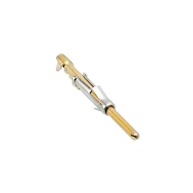
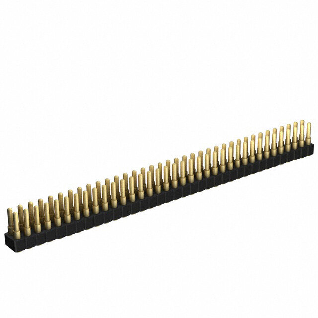
A N - 2 0 2 5 30112711 2. 1 E R U G FI 7 www.national.com
5 2 0 Bill of Materials 2 - N # Designator Qty Part # Description A 1 U1 1 NSC LM5039MH LM5039 Controller 2 U2 1 NSC LM5110-1M LM5110-1M Dual Driver 3 U3 1 NSC LM8261M5 LM8261M5 Op Amp 4 U5 1 NSC LM4041AIM3-.12 LM4041AIM3-1.2 Ref Amp 5 U4 1 NEC PS2811-1M Opto-Coupler PS2811-1M 6 C21 1 TDK C1608COG1H470J Cer Cap 47pF 50V COG 7 C26 1 TDK C1608COG1H151J Cer Cap 150pF 50V COG 8 C34 1 TDK C1608COG1H471J Cer Cap 470pF 50V COG 9 C19, C37 2 TDK C1608X7R1H102K Cer Cap 1000pF 50V X7R 10 C27 2 TDK C1608COG1H222J Cer Cap 2200pF 50V COG 11 C28 1 TDK C1608COG1H682J Cer Cap 6800pF 50V COG 12 C20, C23, C29, 1 TDK C1608X7R1E473K Cer Cap 0.047uF 25V COG C30 13 C2, C33, C31, 3 TDK C1608X7R1H104K Cer Cap 0.1uF 50V X7R C35 14 C25 2 TDK C1608X7R1C105K Cer Cap 1.0uF 16V X7R 15 C36 3 TDK C1608X7R1C474K Cer Cap 0.47uF 50V X7R 16 C32 1 Vishay CRCW06030000Z0TA Res 0 Ohm 0.1W,5% 17 C39 2 TDK C2012x714224K Cer Cap 0.22uF 25V COG 18 C15, C16 2 KEMT C0805C471M5RAC Cer Cap 470pF 50V COG 19 C17, C24 2 TDK C2012X7R2A104K Cer Cap 0.1uF 100V X7R 20 C7 1 TDK C2012X7R1H334K Cer Cap 0.33uF 50V X7R 21 C1, C22 2 TDK C2012X7R1C225K Cer Cap 2.2uF 16V X7R 22 C18 1 TDK C3216X7R1C475K Cer Cap 4.7uF 16V X7R 23 C11–C14 4 TDK C3216X5R0J226M Cer Cap 22uF 6.3V X5R 24 C38 1 TDK C4532X7R3D222K Cer Cap 2200pF 2000V X7R 25 C3–C6 4 TDK C4532X7R1H685M Cer Cap 6.8uF 50V X7R 26 C8–C10 3 Sanyo 6TPE220MI POSCAP 220uF 6.3V 27 R12 1 Vishay CRCW06035R60FKTA Res 5.6 Ohm 0.1W 1% 28 R17, R35 2 Vishay CRCW060310R0F Res 10 Ohm 0.1W 1% 29 R25, R27, R28 3 Vishay CRCW06031000F Res 100 Ohm 0.1W 1% 30 R21 1 Vishay CRCW06035490F Res 549 Ohm 0.1W 1% 31 R13–14, R18–19 4 Vishay CRCW06031001F Res 1K Ohm 0.1W 1% 32 R24 1 NU NU 33 R31 1 Vishay CRCW06032001F Res 2.0K Ohm 0.1W 1% 34 R20 1 Vishay CRCW06034121F Res 4.12K Ohm 0.1W 1% 35 R32 1 Vishay CRCW06035111F Res 5.11K Ohm 0.1W 1% 36 R22 1 Vishay CRCW06038061F Res 8.06K Ohm 0.1W 1% 37 R7, R30 2 Vishay CRCW06031002F Res 10K Ohm 0.1W 1% 38 R26 1 Vishay CRCW06031022F Res 10.2K Ohm 0.1W 1% 39 R33 1 Vishay CRCW06032492F Res 24.9K Ohm 0.1W 1% 40 R29 1 Vishay CRCW06031502F Res 15K Ohm 0.1W 1% 41 R34 1 Vishay CRCW06032002F Res 20K Ohm 0.1W 1% 42 R23 1 Vishay CRCW06032552F Res 25.5K Ohm 0.1W 1% 43 R3, R4 2 Vishay CRCW06031003F Res 100K Ohm 0.1W 1% 44 R1, R11, R15 3 Vishay CRCW080510R0F Res 10 OHM 1/10W 1% 45 R5 1 Vishay CRCW080549R9F Res 49.9 OHM 1/10W 1% 46 R2 1 Vishay CRCW08052001F Res 2K OHM 1/10W 1% 47 R6 1 Vishay CRCW08051002F Res 10K OHM 1/10W 1% www.national.com 8
A N 48 R16 1 Vishay CRCW08056492F Res 64.9K OHM 1/10W 1% - 2 49 R10 2 Vishay CRCW08051003F Res 100K OHM 1/10W 1% 0 2 50 R8, R9 2 Vishay CRCW201010R0F Res 10 OHM 1% 5 51 D1 1 BAV70-TP Schottky, Diode, 75V 150mA 52 D2, D4 2 Central CMDD4448 Diode, 75V 250mA 53 D3 1 BAT54A Schottky Diode, 30V 200mA 54 BR1 1 BAT54BRW Diodes, Rectifier, Bridge, 30V 55 Z1 1 Central CMPZ4694 Zener 8.2V 5% 56 Z2 1 Central CMPZ4698 Zener 11V 5% 57 Q1, Q2 2 Vishay Si7456DP N-FET 100V 25m ohm 58 Q4–7 4 Vishay Si7336ADP N-FET 30V 3m ohm 59 Q3, Q8 2 ZETEX FCX690B NPN, ZETEX 45V 2A 60 L1 1 TDK RLF7030T-2R2M5R4 Inductor 2.2uH 5.4A 61 L2 1 Coilcraft SER2010-122MX Inductor 1.2uH 37A 62 T1 1 Coilcraft DA2025-AL Transformer 8:5:2:2 63 T2 1 Pulse Engr P8208 Current XFR 100:1, 10A 64 T3, T4 2 Coilcraft DA2319-ALB Gate XFR 1:1 65 J1–3, J5–7 6 Mill-Max 3104-2-00-80-00-00-08-0. Test Pin, Brick 66 J4, J8 2 Mill-Max 3231-2-00-01-00-00-08-0 Test Pin, Brick 9 www.national.com
5 2 0 2 PCB Layouts - N A 30112713 Top Silk 30112714 Bottom Silk www.national.com 10
A N - 2 0 2 5 30112715 Top Side 30112716 Layer 2 11 www.national.com
5 2 0 2 - N A 30112717 Layer 3 30112718 Layer 4 www.national.com 12
A N - 2 0 2 5 30112719 Layer 5 30112720 Bottom 13 www.national.com
d r a Notes o B n o ti For more National Semiconductor product information and proven design tools, visit the following Web sites at: a www.national.com u al Products Design Support v Amplifiers www.national.com/amplifiers WEBENCH® Tools www.national.com/webench E Audio www.national.com/audio App Notes www.national.com/appnotes 9 3 Clock and Timing www.national.com/timing Reference Designs www.national.com/refdesigns 0 5 Data Converters www.national.com/adc Samples www.national.com/samples M Interface www.national.com/interface Eval Boards www.national.com/evalboards L LVDS www.national.com/lvds Packaging www.national.com/packaging Power Management www.national.com/power Green Compliance www.national.com/quality/green Switching Regulators www.national.com/switchers Distributors www.national.com/contacts LDOs www.national.com/ldo Quality and Reliability www.national.com/quality LED Lighting www.national.com/led Feedback/Support www.national.com/feedback Voltage References www.national.com/vref Design Made Easy www.national.com/easy PowerWise® Solutions www.national.com/powerwise Applications & Markets www.national.com/solutions Serial Digital Interface (SDI) www.national.com/sdi Mil/Aero www.national.com/milaero Temperature Sensors www.national.com/tempsensors SolarMagic™ www.national.com/solarmagic PLL/VCO www.national.com/wireless PowerWise® Design www.national.com/training University THE CONTENTS OF THIS DOCUMENT ARE PROVIDED IN CONNECTION WITH NATIONAL SEMICONDUCTOR CORPORATION (“NATIONAL”) PRODUCTS. NATIONAL MAKES NO REPRESENTATIONS OR WARRANTIES WITH RESPECT TO THE ACCURACY OR COMPLETENESS OF THE CONTENTS OF THIS PUBLICATION AND RESERVES THE RIGHT TO MAKE CHANGES TO SPECIFICATIONS AND PRODUCT DESCRIPTIONS AT ANY TIME WITHOUT NOTICE. NO LICENSE, WHETHER EXPRESS, IMPLIED, ARISING BY ESTOPPEL OR OTHERWISE, TO ANY INTELLECTUAL PROPERTY RIGHTS IS GRANTED BY THIS DOCUMENT. TESTING AND OTHER QUALITY CONTROLS ARE USED TO THE EXTENT NATIONAL DEEMS NECESSARY TO SUPPORT NATIONAL’S PRODUCT WARRANTY. EXCEPT WHERE MANDATED BY GOVERNMENT REQUIREMENTS, TESTING OF ALL PARAMETERS OF EACH PRODUCT IS NOT NECESSARILY PERFORMED. NATIONAL ASSUMES NO LIABILITY FOR APPLICATIONS ASSISTANCE OR BUYER PRODUCT DESIGN. BUYERS ARE RESPONSIBLE FOR THEIR PRODUCTS AND APPLICATIONS USING NATIONAL COMPONENTS. PRIOR TO USING OR DISTRIBUTING ANY PRODUCTS THAT INCLUDE NATIONAL COMPONENTS, BUYERS SHOULD PROVIDE ADEQUATE DESIGN, TESTING AND OPERATING SAFEGUARDS. EXCEPT AS PROVIDED IN NATIONAL’S TERMS AND CONDITIONS OF SALE FOR SUCH PRODUCTS, NATIONAL ASSUMES NO LIABILITY WHATSOEVER, AND NATIONAL DISCLAIMS ANY EXPRESS OR IMPLIED WARRANTY RELATING TO THE SALE AND/OR USE OF NATIONAL PRODUCTS INCLUDING LIABILITY OR WARRANTIES RELATING TO FITNESS FOR A PARTICULAR PURPOSE, MERCHANTABILITY, OR INFRINGEMENT OF ANY PATENT, COPYRIGHT OR OTHER INTELLECTUAL PROPERTY RIGHT. LIFE SUPPORT POLICY NATIONAL’S PRODUCTS ARE NOT AUTHORIZED FOR USE AS CRITICAL COMPONENTS IN LIFE SUPPORT DEVICES OR SYSTEMS WITHOUT THE EXPRESS PRIOR WRITTEN APPROVAL OF THE CHIEF EXECUTIVE OFFICER AND GENERAL COUNSEL OF NATIONAL SEMICONDUCTOR CORPORATION. As used herein: Life support devices or systems are devices which (a) are intended for surgical implant into the body, or (b) support or sustain life and whose failure to perform when properly used in accordance with instructions for use provided in the labeling can be reasonably expected to result in a significant injury to the user. A critical component is any component in a life support device or system whose failure to perform can be reasonably expected to cause the failure of the life support device or system or to affect its safety or effectiveness. National Semiconductor and the National Semiconductor logo are registered trademarks of National Semiconductor Corporation. All other brand or product names may be trademarks or registered trademarks of their respective holders. Copyright© 2010 National Semiconductor Corporation 5 For the most current product information visit us at www.national.com 2 0 National Semiconductor National Semiconductor Europe National Semiconductor Asia National Semiconductor Japan 2 Americas Technical Technical Support Center Pacific Technical Support Center Technical Support Center - Support Center Email: europe.support@nsc.com Email: ap.support@nsc.com Email: jpn.feedback@nsc.com N Email: support@nsc.com A Tel: 1-800-272-9959 www.national.com
IMPORTANTNOTICE TexasInstrumentsIncorporatedanditssubsidiaries(TI)reservetherighttomakecorrections,modifications,enhancements,improvements, andotherchangestoitsproductsandservicesatanytimeandtodiscontinueanyproductorservicewithoutnotice.Customersshould obtainthelatestrelevantinformationbeforeplacingordersandshouldverifythatsuchinformationiscurrentandcomplete.Allproductsare soldsubjecttoTI’stermsandconditionsofsalesuppliedatthetimeoforderacknowledgment. TIwarrantsperformanceofitshardwareproductstothespecificationsapplicableatthetimeofsaleinaccordancewithTI’sstandard warranty.TestingandotherqualitycontroltechniquesareusedtotheextentTIdeemsnecessarytosupportthiswarranty.Exceptwhere mandatedbygovernmentrequirements,testingofallparametersofeachproductisnotnecessarilyperformed. TIassumesnoliabilityforapplicationsassistanceorcustomerproductdesign.Customersareresponsiblefortheirproductsand applicationsusingTIcomponents.Tominimizetherisksassociatedwithcustomerproductsandapplications,customersshouldprovide adequatedesignandoperatingsafeguards. TIdoesnotwarrantorrepresentthatanylicense,eitherexpressorimplied,isgrantedunderanyTIpatentright,copyright,maskworkright, orotherTIintellectualpropertyrightrelatingtoanycombination,machine,orprocessinwhichTIproductsorservicesareused.Information publishedbyTIregardingthird-partyproductsorservicesdoesnotconstitutealicensefromTItousesuchproductsorservicesora warrantyorendorsementthereof.Useofsuchinformationmayrequirealicensefromathirdpartyunderthepatentsorotherintellectual propertyofthethirdparty,oralicensefromTIunderthepatentsorotherintellectualpropertyofTI. ReproductionofTIinformationinTIdatabooksordatasheetsispermissibleonlyifreproductioniswithoutalterationandisaccompanied byallassociatedwarranties,conditions,limitations,andnotices.Reproductionofthisinformationwithalterationisanunfairanddeceptive businesspractice.TIisnotresponsibleorliableforsuchaltereddocumentation.Informationofthirdpartiesmaybesubjecttoadditional restrictions. ResaleofTIproductsorserviceswithstatementsdifferentfromorbeyondtheparametersstatedbyTIforthatproductorservicevoidsall expressandanyimpliedwarrantiesfortheassociatedTIproductorserviceandisanunfairanddeceptivebusinesspractice.TIisnot responsibleorliableforanysuchstatements. TIproductsarenotauthorizedforuseinsafety-criticalapplications(suchaslifesupport)whereafailureoftheTIproductwouldreasonably beexpectedtocauseseverepersonalinjuryordeath,unlessofficersofthepartieshaveexecutedanagreementspecificallygoverning suchuse.Buyersrepresentthattheyhaveallnecessaryexpertiseinthesafetyandregulatoryramificationsoftheirapplications,and acknowledgeandagreethattheyaresolelyresponsibleforalllegal,regulatoryandsafety-relatedrequirementsconcerningtheirproducts andanyuseofTIproductsinsuchsafety-criticalapplications,notwithstandinganyapplications-relatedinformationorsupportthatmaybe providedbyTI.Further,BuyersmustfullyindemnifyTIanditsrepresentativesagainstanydamagesarisingoutoftheuseofTIproductsin suchsafety-criticalapplications. TIproductsareneitherdesignednorintendedforuseinmilitary/aerospaceapplicationsorenvironmentsunlesstheTIproductsare specificallydesignatedbyTIasmilitary-gradeor"enhancedplastic."OnlyproductsdesignatedbyTIasmilitary-grademeetmilitary specifications.BuyersacknowledgeandagreethatanysuchuseofTIproductswhichTIhasnotdesignatedasmilitary-gradeissolelyat theBuyer'srisk,andthattheyaresolelyresponsibleforcompliancewithalllegalandregulatoryrequirementsinconnectionwithsuchuse. TIproductsareneitherdesignednorintendedforuseinautomotiveapplicationsorenvironmentsunlessthespecificTIproductsare designatedbyTIascompliantwithISO/TS16949requirements.Buyersacknowledgeandagreethat,iftheyuseanynon-designated productsinautomotiveapplications,TIwillnotberesponsibleforanyfailuretomeetsuchrequirements. FollowingareURLswhereyoucanobtaininformationonotherTexasInstrumentsproductsandapplicationsolutions: Products Applications Audio www.ti.com/audio CommunicationsandTelecom www.ti.com/communications Amplifiers amplifier.ti.com ComputersandPeripherals www.ti.com/computers DataConverters dataconverter.ti.com ConsumerElectronics www.ti.com/consumer-apps DLP®Products www.dlp.com EnergyandLighting www.ti.com/energy DSP dsp.ti.com Industrial www.ti.com/industrial ClocksandTimers www.ti.com/clocks Medical www.ti.com/medical Interface interface.ti.com Security www.ti.com/security Logic logic.ti.com Space,AvionicsandDefense www.ti.com/space-avionics-defense PowerMgmt power.ti.com TransportationandAutomotive www.ti.com/automotive Microcontrollers microcontroller.ti.com VideoandImaging www.ti.com/video RFID www.ti-rfid.com OMAPMobileProcessors www.ti.com/omap WirelessConnectivity www.ti.com/wirelessconnectivity TIE2ECommunityHomePage e2e.ti.com MailingAddress:TexasInstruments,PostOfficeBox655303,Dallas,Texas75265 Copyright©2011,TexasInstrumentsIncorporated

 Datasheet下载


.jpg)