ICGOO在线商城 > 集成电路(IC) > PMIC - 稳压器 - DC DC 开关稳压器 > LM5008SD

 Datasheet下载
- 型号: LM5008SD
- 制造商: Texas Instruments
- 库位|库存: xxxx|xxxx
- 要求:
| 数量阶梯 | 香港交货 | 国内含税 |
| +xxxx | $xxxx | ¥xxxx |
查看当月历史价格
查看今年历史价格
LM5008SD产品简介:
ICGOO电子元器件商城为您提供LM5008SD由Texas Instruments设计生产,在icgoo商城现货销售,并且可以通过原厂、代理商等渠道进行代购。 LM5008SD价格参考。Texas InstrumentsLM5008SD封装/规格:PMIC - 稳压器 - DC DC 开关稳压器, 可调式 降压 开关稳压器 IC 正 2.5V 1 输出 350mA 8-WDFN 裸露焊盘。您可以下载LM5008SD参考资料、Datasheet数据手册功能说明书,资料中有LM5008SD 详细功能的应用电路图电压和使用方法及教程。
| 参数 | 数值 |
| 产品目录 | 集成电路 (IC) |
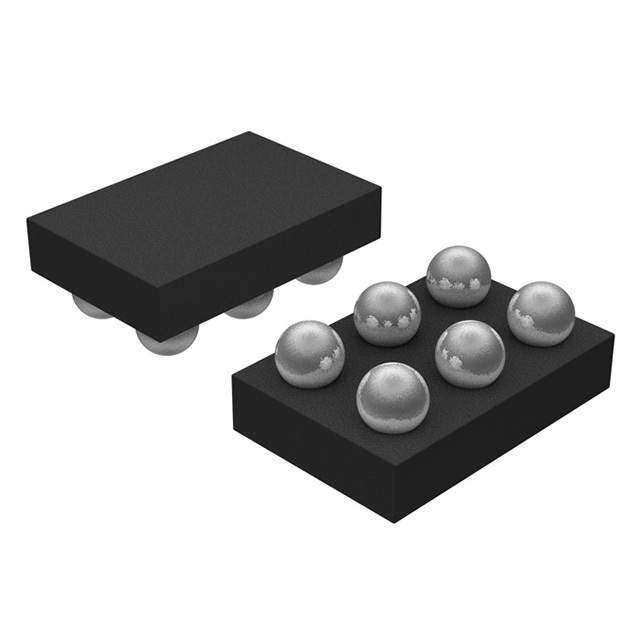
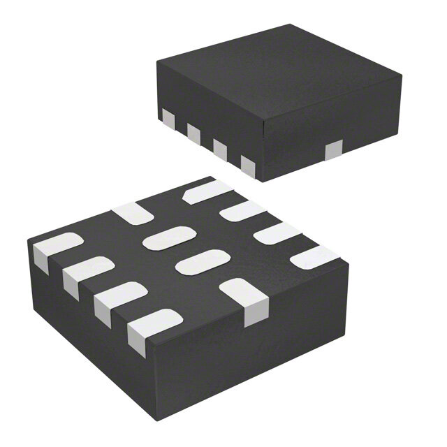
| 描述 | IC REG BUCK ADJ 0.35A DL 8LLP |
| 产品分类 | |
| 品牌 | Texas Instruments |
| 数据手册 | |
| 产品图片 |
|
| 产品型号 | LM5008SD |
| PWM类型 | 混合物 |
| rohs | 含铅 / 不符合限制有害物质指令(RoHS)规范要求 |
| RoHS指令信息 | |
| 产品系列 | - |
| 供应商器件封装 | 8-LLP-EP(4x4) |
| 其它名称 | 296-35464-2 |
| 包装 | 带卷 (TR) |
| 同步整流器 | 无 |
| 安装类型 | 表面贴装 |
| 封装/外壳 | 8-WDFN 裸露焊盘 |
| 工作温度 | -40°C ~ 125°C |
| 标准包装 | 1,000 |
| 电压-输入 | 9.5 V ~ 95 V |
| 电压-输出 | 2.5 V ~ 75 V |
| 电流-输出 | 350mA |
| 类型 | 降压(降压) |
| 设计资源 | http://www.digikey.com/product-highlights/cn/zh/texas-instruments-webench-design-center/3176 |
| 输出数 | 1 |
| 输出类型 | 可调式 |
| 配用 | /product-detail/zh/LM5008EVAL/LM5008EVAL-ND/695388/product-detail/zh/LM5008EVAL%2FNOPB/LM5008EVAL%2FNOPB-ND/3179108 |
| 频率-开关 | 50kHz ~ 600kHz |


- 商务部:美国ITC正式对集成电路等产品启动337调查
- 曝三星4nm工艺存在良率问题 高通将骁龙8 Gen1或转产台积电
- 太阳诱电将投资9.5亿元在常州建新厂生产MLCC 预计2023年完工
- 英特尔发布欧洲新工厂建设计划 深化IDM 2.0 战略
- 台积电先进制程称霸业界 有大客户加持明年业绩稳了
- 达到5530亿美元!SIA预计今年全球半导体销售额将创下新高
- 英特尔拟将自动驾驶子公司Mobileye上市 估值或超500亿美元
- 三星加码芯片和SET,合并消费电子和移动部门,撤换高东真等 CEO
- 三星电子宣布重大人事变动 还合并消费电子和移动部门
- 海关总署:前11个月进口集成电路产品价值2.52万亿元 增长14.8%


PDF Datasheet 数据手册内容提取
Product Order Technical Tools & Support & Folder Now Documents Software Community LM5008 SNVS280I–APRIL2004–REVISEDOCTOBER2018 LM5008 95-V, 350-mA, Constant On-Time DC/DC Buck Switching Regulator 1 Features 3 Description • OperatingInputVoltageRange:6Vto95V The LM5008 350-mA step-down switching converter 1 features all of the functions needed to implement a • Integrated100-V,N-ChannelBuckSwitch low-cost and efficient buck regulator. This high- • InternalVCCRegulator voltage converter has an integrated 100-V N-channel • NoLoopCompensationRequired buck switch and operates over an input voltage range of 9 V to 95 V. The device is easy to implement and • Ultra-FastTransientResponse is provided in the 8-pin VSSOP and the thermally • On-TimeVariesInverselyWithLineVoltage enhanced 8-pin WSON packages. The converter • OperatingFrequencyRemainsConstantWith usesahystereticcontrolschemewithaPWMon-time VaryingLineVoltageandLoadCurrent inversely proportional to V . This feature allows the IN operatingfrequencytoremainrelativelyconstant.The • AdjustableOutputVoltage hysteretic control requires no loop compensation. An • HighlyEfficientOperation intelligent current limit is implemented with forced off- • PrecisionInternalReference time, which is inversely proportional to V . This OUT • LowBiasCurrent scheme ensures short-circuit protection while providing minimum foldback. Other protection • IntelligentCurrentLimitProtection features include: thermal shutdown, V undervoltage CC • ThermalShutdown lockout, gate drive undervoltage lockout, and • 8-PinVSSOPandWSONPackages maximumdutycyclelimiter. • CreateaCustomDesignUsingtheLM5008With DeviceInformation(1) theWEBENCH®PowerDesigner PARTNUMBER PACKAGE BODYSIZE(NOM) 2 Applications VSSOP(8) 3.00mm×3.00mm LM5008 WSON(8) 4.00mm×4.00mm • Non-IsolatedTelecommunicationBuckRegulators (1) For all available packages, see the orderable addendum at • SecondaryHigh-VoltagePostRegulators theendofthedatasheet. • 48-VAutomotiveSystems TypicalApplicationCircuitandBlockDiagram 7V SERIES LM5008 9.5 -95V REGULATOR Input 8 VCC 7 VIN SD C1 C5 UVLO STHHUETRDMOAWLN C3 RON ONTSITMAERRT 6 SD / RCoOnMPLETE BST 2 SHUTDOWN RON OCVOEMRP-VAORALTTAOGRE 300 SnTsA MRITN OFF UVLO SD VIN + TIMER DRIVER C4 2.875V - COMPLETE LEVEL 2.5V SHIFT SW 1 L1 5 + SSETQ VOUT1 - FB CROEMGPUALRAATITOONR RCLRQ R1 RCL 3 RCL FRBCLCUORFRFECTNIOMTMELPSRIMLTEIATTRET +-0.50A CSSUBWERUINRTCSCEKEHNT D1 R3VOUT2 4 RTN R2 C2 Copyright © 2016,Texas Instruments Incorporated 1 An IMPORTANT NOTICE at the end of this data sheet addresses availability, warranty, changes, use in safety-critical applications, intellectualpropertymattersandotherimportantdisclaimers.PRODUCTIONDATA.
LM5008 SNVS280I–APRIL2004–REVISEDOCTOBER2018 www.ti.com Table of Contents 1 Features.................................................................. 1 7.4 DeviceFunctionalModes.......................................11 2 Applications........................................................... 1 8 ApplicationandImplementation........................ 12 3 Description............................................................. 1 8.1 ApplicationInformation............................................12 4 RevisionHistory..................................................... 2 8.2 TypicalApplication..................................................12 5 PinConfigurationandFunctions......................... 3 9 PowerSupplyRecommendations...................... 16 6 Specifications......................................................... 4 10 Layout................................................................... 17 6.1 AbsoluteMaximumRatings......................................4 10.1 LayoutGuidelines.................................................17 6.2 ESDRatings ............................................................4 10.2 LayoutExamples...................................................17 6.3 RecommendedOperatingConditions.......................4 11 DeviceandDocumentationSupport................. 18 6.4 ThermalInformation..................................................4 11.1 DeviceSupport ....................................................18 6.5 ElectricalCharacteristics...........................................5 11.2 DocumentationSupport........................................18 6.6 SwitchingCharacteristics..........................................5 11.3 ReceivingNotificationofDocumentationUpdates19 6.7 TypicalCharacteristics..............................................6 11.4 CommunityResources..........................................19 7 DetailedDescription.............................................. 7 11.5 Trademarks...........................................................19 7.1 Overview...................................................................7 11.6 ElectrostaticDischargeCaution............................19 7.2 FunctionalBlockDiagram.........................................7 11.7 Glossary................................................................19 7.3 FeatureDescription...................................................8 12 Mechanical,Packaging,andOrderable Information........................................................... 19 4 Revision History NOTE:Pagenumbersforpreviousrevisionsmaydifferfrompagenumbersinthecurrentversion. ChangesfromRevisionH(December2016)toRevisionI Page • AddedlinksforWEBENCH ................................................................................................................................................... 1 • ChangedVSSOP-8bodysizeto3mm×3mminDeviceInformation.................................................................................. 1 • ChangedLayoutGuidelines ................................................................................................................................................ 17 ChangesfromRevisionG(March2013)toRevisionH Page • AddedESDRatingstable,FeatureDescriptionsection,DeviceFunctionalModes,ApplicationandImplementation section,PowerSupplyRecommendationssection,Layoutsection,DeviceandDocumentationSupportsection,and Mechanical,Packaging,andOrderableInformationsection.................................................................................................. 1 • DeletedLeadtemperature,soldering(260°Cmaximum)....................................................................................................... 4 • ChangedR valuesFrom:200°C/WTo:139.7°C/W(VSSOP)andFrom:40°C/WTo:42°C/W(WSON).......................... 4 θJA ChangesfromRevisionF(March2013)toRevisionG Page • ChangedlayoutofNationalSemiconductorDataSheettoTIformat.................................................................................... 1 2 SubmitDocumentationFeedback Copyright©2004–2018,TexasInstrumentsIncorporated ProductFolderLinks:LM5008
LM5008 www.ti.com SNVS280I–APRIL2004–REVISEDOCTOBER2018 5 Pin Configuration and Functions DGKPackage 8-PinVSSOP NGUPackage TopView 8-PinWSON TopView SW 1 8 VIN SW 1 8 VIN BST 2 7 VCC BST 2 7 VCC RCL 3 6 RT/SD EP RCL 3 6 RT/SD RTN 4 5 FB RTN 4 5 FB Not to scale Not to scale PinFunctions PIN TYPE DESCRIPTION NO. NAME Switchingnode:powerswitchingnode.Connecttotheoutputinductor,re-circulatingdiode,andbootstrap 1 SW P capacitor. Boostpin(bootstrapcapacitorinput):anexternalcapacitorisrequiredbetweentheBSTandtheSWpins.A 2 BST I 0.01-µFceramiccapacitorisrecommended.AninternaldiodechargesthecapacitorfromV . CC CurrentlimitOFFtimesetpin:aresistorbetweenthispinandRTNsetstheoff-timewhencurrentlimitis 3 R I detected.Theoff-timeispresetto35µsifFB=0V. CL Toff=10–5/(0.285+(FB/6.35×10−6×R )) CL 4 RTN G Groundpin:groundfortheentirecircuit. Feedbackinputfromregulatedoutput:thispinisconnectedtotheinvertinginputoftheinternalregulation 5 FB I comparator.Theregulationthresholdis2.5V. On-timesetpin:aresistorbetweenthispinandV setstheswitchon-timeasafunctionofV .The IN IN minimumrecommendedon-timeis400nsatthemaximuminputvoltage.Thispincanbeusedforremote 6 R /SD I ON shutdown. Ton=1.25×10⁻¹⁰R /V ON IN Outputfromtheinternalhighvoltageseriespassregulator.Regulatedat7V.Ifanauxiliaryvoltageis availabletoraisethevoltageonthispin,abovetheregulationsetpoint(7V),theinternalseriespass 7 V P regulatorwillshutdown,reducingtheICpowerdissipation.Donotexceed14V.Thisvoltageprovidesgate CC drivepowerfortheinternalbuckswitch.AninternaldiodeisprovidedbetweenthispinandtheBSTpin.A local0.1-µFdecouplingcapacitorisrecommended.Seriespassregulatoriscurrentlimitedto10mA. 8 V P Inputvoltage:recommendedoperatingrangeis9.5Vto95V. IN Exposedpad:theexposedpadhasnoelectricalcontact.Connecttosystemgroundplaneforreduced — EP G thermalresistance(WSONpackageonly). Copyright©2004–2018,TexasInstrumentsIncorporated SubmitDocumentationFeedback 3 ProductFolderLinks:LM5008
LM5008 SNVS280I–APRIL2004–REVISEDOCTOBER2018 www.ti.com 6 Specifications 6.1 Absolute Maximum Ratings overoperatingfree-airtemperaturerange(unlessotherwisenoted)(1) MIN MAX UNIT V toGND –0.3 100 V IN BSTtoGND –0.3 114 V SWtoGND(steady-state) –1 V BSTtoV 100 V CC BSTtoSW 14 V V toGND 14 V CC AllotherinputstoGND –0.3 7 V Storagetemperature,T –55 150 °C stg (1) StressesbeyondthoselistedunderAbsoluteMaximumRatingsmaycausepermanentdamagetothedevice.Thesearestressratings only,whichdonotimplyfunctionaloperationofthedeviceattheseoranyotherconditionsbeyondthoseindicatedunderRecommended OperatingConditions.Exposuretoabsolute-maximum-ratedconditionsforextendedperiodsmayaffectdevicereliability. 6.2 ESD Ratings VALUE UNIT Human-bodymodel(HBM),perANSI/ESDA/JEDECJS-001(1)(2) ±2000 V Electrostaticdischarge V (ESD) Charged-devicemodel(CDM),perJEDECspecificationJESD22-C101(3) ±750 (1) JEDECdocumentJEP155statesthat500-VHBMallowssafemanufacturingwithastandardESDcontrolprocess. (2) Thehumanbodymodelisa100-pFcapacitordischargedthrougha1.5-kΩresistorintoeachpin. (3) JEDECdocumentJEP157statesthat250-VCDMallowssafemanufacturingwithastandardESDcontrolprocess. 6.3 Recommended Operating Conditions overoperatingfree-airtemperaturerange(unlessotherwisenoted) MIN MAX UNIT V 9.5 95 V IN Operatingjunctiontemperature,T –40 125 °C J 6.4 Thermal Information LM5008 THERMALMETRIC(1) DGK(VSSOP) NGU(WSON) UNIT 8PINS 8PINS R Junction-to-ambientthermalresistance 139.7 42 °C/W θJA R Junction-to-case(top)thermalresistance 51.2 27.6 °C/W θJC(top) R Junction-to-boardthermalresistance 70.5 18.5 °C/W θJB ψ Junction-to-topcharacterizationparameter 3.4 0.3 °C/W JT ψ Junction-to-boardcharacterizationparameter 69.5 18.5 °C/W JB R Junction-to-case(bottom)thermalresistance — 4.3 °C/W θJC(bot) (1) Formoreinformationabouttraditionalandnewthermalmetrics,seetheSemiconductorandICPackageThermalMetricsapplication report. 4 SubmitDocumentationFeedback Copyright©2004–2018,TexasInstrumentsIncorporated ProductFolderLinks:LM5008
LM5008 www.ti.com SNVS280I–APRIL2004–REVISEDOCTOBER2018 6.5 Electrical Characteristics SpecificationsareforT =25°CandV =48V(unlessotherwisestated)(1). J IN PARAMETER TESTCONDITIONS MIN TYP MAX UNIT VCCSUPPLY TJ=25°C 7 VCCReg VCCregulatoroutput V TJ=–40°Cto125°C 6.6 7.4 VCCcurrentlimit(2) 9.5 mA VCCundervoltagelockoutvoltage VCCincreasing 6.3 V VCCundervoltagehysteresis 200 mV VCCUVLOdelay(filter) 100-mVoverdrive 10 µs TJ=25°C 485 IINoperatingcurrent Non-switching,FB=3V µA TJ=–40°Cto125°C 675 TJ=25°C 76 IINshutdowncurrent RON/SD=0V µA TJ=–40°Cto125°C 150 CURRENTLIMIT TJ=25°C 0.51 Currentlimitthreshold A TJ=–40°Cto125°C 0.41 0.61 Currentlimitresponsetime Iswitchoverdrive=0.1A,timetoswitchoff 400 ns OFFtimegenerator(test1) FB=0V,RCL=100K 35 µs OFFtimegenerator(test2) FB=2.3V,RCL=100K 2.56 µs ON-TIMEGENERATOR TJ=25°C 2.77 TON–1 VIN=10V,RON=200K µs TJ=–40°Cto125°C 2.15 3.5 TJ=25°C 300 TON–2 VIN=95V,RON=200K ns TJ=–40°Cto125°C 200 420 TJ=25°C 0.7 Remoteshutdownthreshold Rising V TJ=–40°Cto125°C 0.4 1.05 Remoteshutdownhysteresis 35 mV MINIMUMOFF-TIME Minimumoff-timer FB=0V 300 ns REGULATIONANDOVCOMPARATORS Internalreference,trippointfor TJ=25°C 2.5 FBreferencethreshold V switchON TJ=–40°Cto125°C 2.445 2.55 FBovervoltagethreshold TrippointforswitchOFF 2.875 V FBbiascurrent 100 nA THERMALSHUTDOWN Tsd Thermalshutdowntemperature 165 °C Thermalshutdownhysteresis 25 °C (1) AllelectricalcharacteristicshavingroomtemperaturelimitsaretestedduringproductionwithT =T =25°C.Allhotandcoldlimitsare A J specifiedbycorrelatingtheelectricalcharacteristicstoprocessandtemperaturevariationsandapplyingstatisticalprocesscontrol. (2) TheV outputisintendedasaselfbiasfortheinternalgatedrivepowerandcontrolcircuits.Devicethermallimitationslimitexternal CC loading. 6.6 Switching Characteristics overoperatingfree-airtemperaturerange(unlessotherwisenoted) PARAMETER TESTCONDITIONS MIN TYP MAX UNIT BuckswitchRDS(on) ITEST=200mA(1) TJ=25°C 1.15 Ω TJ=–40°Cto125°C 2.47 TJ=25°C 4.5 GatedriveUVLO VBST–VSWrising V TJ=–40°Cto125°C 3.4 5.5 GatedriveUVLOhysteresis 430 mV (1) Fordevicesprocuredinthe8-pinWSONpackagetheR limitsarespecifiedbydesigncharacterizationdataonly. DS(on) Copyright©2004–2018,TexasInstrumentsIncorporated SubmitDocumentationFeedback 5 ProductFolderLinks:LM5008
LM5008 SNVS280I–APRIL2004–REVISEDOCTOBER2018 www.ti.com 6.7 Typical Characteristics 2.0 8 7 )Am 1.8 6 RON = 500k ( T N 5 E 1.6 R s) RUC TU 1.4 T (PON 34 300k P N I C 2 100k C 1.2 I 1 1.0 0 0 20 40 60 80 100 8 9 10 11 12 13 14 EXTERNALLY APPLIED VCC (V) VIN (V) Figure1.ICCCurrentvsAppliedVCCVoltage Figure2.On-TimevsInputVoltageandRON 700 35 48V 60V 80V )zH 600 )sP 30 k( Y 500 Max VIN ( EM 25 CN = 30V IT EUQ 400 95V FFO 20 E T RF MN 300 IMIL T 15 300k RCL = 500k UM 200 NER 10 IXA RU 100k M 100 C 5 50k 0 0 0 2.5 5.0 10 15 20 0 0.5 1.0 1.5 2.0 2.5 VOUT (V) VFB (V) Figure3.MaximumFrequencyvsVOUTandVIN Figure4.CurrentLimitOff-TimevsVFBandRCL 100 10.2 VIN = 15V VOUT1 90 VIN = 48V 10.0 )%( Y 80 VIN = 95V V) 9.8 VOUT2 CN 70 (T 9.6 EIC VOU IFF 60 9.4 E 50 9.2 VIN = 48V 40 9.0 100 200 300 0 100 200 300 LOAD CURRENT (mA) LOAD CURRENT (mA) Figure5.EfficiencyvsLoadCurrentvsVIN Figure6.OutputVoltagevsLoadCurrent (CircuitofFigure10) (CircuitofFigure10) 6 SubmitDocumentationFeedback Copyright©2004–2018,TexasInstrumentsIncorporated ProductFolderLinks:LM5008
LM5008 www.ti.com SNVS280I–APRIL2004–REVISEDOCTOBER2018 7 Detailed Description 7.1 Overview The LM5008 regulator is an easy-to-use buck DC-DC converter that operates from 9.5-V to 95-V supply voltage. The device is intended for step-down conversions from 12-V, 24-V, and 48-V unregulated, semi-regulated and fully-regulated supply rails. With integrated buck power MOSFET, the LM5008 delivers up to 350-mA DC load currentwithexceptionalefficiencyandlowinputquiescentcurrentinaverysmallsolutionsize. Designed for simple implementation, a nearly fixed-frequency, constant on-time (COT) operation with discontinuous conduction mode (DCM) at light loads is ideal for low-noise, high current, fast transient load requirements.Controlloopcompensationisnotrequiredreducingdesigntimeandexternalcomponentcount. The LM5008 incorporates other features for comprehensive system requirements, including VCC undervoltage lockout (UVLO), gate drive undervoltage lockout, maximum duty cycle limiter, intelligent current limit off timer, a precharge switch, and thermal shutdown with automatic recovery. These features enable a flexible and easy-to- use platform for a wide range of applications. The pin arrangement is designed for simple and optimized PCB layout,requiringonlyafewexternalcomponents. 7.2 Functional Block Diagram 7V SERIES LM5008 9.5 -95V REGULATOR Input 8 VCC 7 VIN SD C1 C5 THERMAL C3 UVLO SHUTDOWN ONTIMER RON START COMPLETE 6 Ron BST 2 SD / RON OVER-VOLTAGE START SD VIN SHUTDOWN COMPARATOR 300 ns MIN OFF UVLO + TIMER DRIVER C4 2.875V - COMPLETE LEVEL 2.5V SHIFT SW 1 L1 5 + S SETQ VOUT1 - FB REGULATION R CLRQ COMPARATOR R1 3 FB COMPLETE R3 RCL RCL RCLCUORFRFETNIMTELSRIMTIATRT +-0.50A CSSUBWERUINRTCSCEKEHNT D1 VOUT2 4 RTN R2 C2 Copyright © 2016,Texas Instruments Incorporated Copyright©2004–2018,TexasInstrumentsIncorporated SubmitDocumentationFeedback 7 ProductFolderLinks:LM5008
LM5008 SNVS280I–APRIL2004–REVISEDOCTOBER2018 www.ti.com 7.3 Feature Description 7.3.1 HystereticControlCircuitOverview The LM5008 is a buck DC-DC regulator that uses a control scheme in which the on-time varies inversely with line voltage (V ). Control is based on a comparator and the on-time one-shot, with the output voltage feedback IN (FB)comparedtoaninternalreference(2.5V).IftheFBlevelisbelowthereferencethebuckswitchisturnedon for a fixed time determined by the line voltage and a programming resistor (R ). Following the ON period, the ON switch remains off for at least the minimum off-timer period of 300 ns. If FB is still below the reference at that time,theswitchturnsonagainforanotheron-timeperiod.Thiswillcontinueuntilregulationisachieved. The LM5008 operates in discontinuous conduction mode at light load currents, and continuous conduction mode at heavy load current. In discontinuous conduction mode, current through the output inductor starts at zero and ramps up to a peak during the on-time, then ramps back to zero before the end of the off-time. The next on-time period starts when the voltage at FB falls below the internal reference; until then, the inductor current remains zero. In this mode the operating frequency is lower than in continuous conduction mode, and varies with load current. Therefore at light loads the conversion efficiency is maintained, because the switching losses reduce with the reduction in load and frequency. The discontinuous operating frequency can be calculated with Equation1. V 2 x L x 1.28 x 10²⁰ OUT F = R x (R )2 L ON where • R =theloadresistance (1) L In continuous conduction mode, current flows continuously through the inductor and never ramps down to zero. In this mode the operating frequency is greater than the discontinuous mode frequency and remains relatively constant with load and line variations. The approximate continuous mode operating frequency can be calculated withEquation2. V OUT F = 1.25 x 10⁻¹⁰ x R ON (2) The output voltage (V ) can be programmed by two external resistors as shown in Functional Block Diagram. OUT TheregulationpointcanbecalculatedwithEquation3. V =2.5×(R1+R2)/R2 (3) OUT All hysteretic regulators regulate the output voltage based on ripple voltage at the feedback input, requiring a minimum amount of ESR for the output capacitor C2. A minimum of 25 mV to 50 mV of ripple voltage at the feedback pin (FB) is required for the LM5008. In cases where the capacitor ESR is too small, additional series resistancemayberequired(R3inFunctionalBlockDiagram). For applications where lower output voltage ripple is required the output can be taken directly from a low-ESR outputcapacitor,asshowninFigure7.However,R3slightlydegradestheloadregulation. L1 SW LM5008 R1 R3 FB VOUT2 R2 C2 Copyright © 2016,Texas Instruments Incorporated Figure7. Low-RippleOutputConfiguration 8 SubmitDocumentationFeedback Copyright©2004–2018,TexasInstrumentsIncorporated ProductFolderLinks:LM5008
LM5008 www.ti.com SNVS280I–APRIL2004–REVISEDOCTOBER2018 Feature Description (continued) 7.3.2 HighVoltageStart-UpRegulator The LM5008 contains an internal high voltage start-up regulator. The input pin (V ) can be connected directly to IN the line voltages up to 95 Volts, with transient capability to 100 V. The regulator is internally current limited to 9.5 mA at V . Upon power up, the regulator sources current into the external capacitor at V (C3). When the CC CC voltageontheV pinreachestheundervoltagelockoutthresholdof6.3V,thebuckswitchisenabled. CC In applications involving a high value for V , where power dissipation in the V regulator is a concern, an IN CC auxiliary voltage can be diode connected to the V pin. Setting the auxiliary voltage to 8 V to 14 V shuts off the CC internal regulator, reducing internal power dissipation. See Figure 8. The current required into the V pin is CC showninFigure1. VCC C3 BST C4 LM5008 L1 D2 SW D1 R1 R3 FB VOUT2 R2 C2 Copyright © 2016,Texas Instruments Incorporated Figure8. Self-BiasedConfiguration 7.3.3 RegulationComparator ThefeedbackvoltageatFBiscomparedtoaninternal2.5-Vreference.Innormaloperation(theoutputvoltageis regulated), an on-time period is initiated when the voltage at FB falls below 2.5 V. The buck switch stays on for the on-time, causing the FB voltage to rise above 2.5 V. After the on-time period, the buck switch stays off until the FB voltage again falls below 2.5 V. During start-up, the FB voltage is below 2.5 V at the end of each on-time, resultingintheminimumoff-timeof300ns.BiascurrentattheFBpinisnominally100nA. 7.3.4 OvervoltageComparator The feedback voltage at FB is compared to an internal 2.875-V reference. If the voltage at FB rises above 2.875 V, the on-time pulse is immediately terminated. This condition can occur if the input voltage, or the output load, changesuddenly.ThebuckswitchwillnotturnonagainuntilthevoltageatFBfallsbelow2.5V. 7.3.5 On-TimeGeneratorandShutdown The on-time for the LM5008 is determined by the R resistor, and is inversely proportional to the input voltage ON (V ), resulting in a nearly constant frequency as V is varied over its range. Equation 4 shows the on-time IN IN equationfortheLM5008. T =1.25×10⁻¹⁰×R /V (4) ON ON IN See Figure 2. R should be selected for a minimum on-time (at maximum V ) greater than 400 ns for proper ON IN current limit operation. This requirement limits the maximum frequency for each application, depending on V IN andV .SeeFigure3. OUT Copyright©2004–2018,TexasInstrumentsIncorporated SubmitDocumentationFeedback 9 ProductFolderLinks:LM5008
LM5008 SNVS280I–APRIL2004–REVISEDOCTOBER2018 www.ti.com Feature Description (continued) The LM5008 can be remotely disabled by taking the R /SD pin to ground. See Figure 9. The voltage at the ON R /SDpinisbetween1.5and3volts,dependingonV andthevalueoftheR resistor. ON IN ON Input Voltage VIN LM5008 RON RON/SD STOP RUN Copyright © 2016,Texas Instruments Incorporated Figure9. ShutdownImplementation 7.3.6 CurrentLimit The LM5008 contains an intelligent current limit off-timer. If the current in the buck switch exceeds 0.5 A the present cycle is immediately terminated, and a non-resetable off-timer is initiated. The length of off-time is controlledbyanexternalresistor(R )andtheFBvoltage(seeFigure4).WhenFB=0V,amaximumoff-timeis CL required, and the time is preset to 35 µs. This condition occurs when the output is shorted, and during the initial part of start-up. This amount of time ensures safe short-circuit operation up to the maximum input voltage of 95 V. In cases of overload where the FB voltage is above zero volts (not a short circuit), the current limit off-time will be less than 35 µs. Reducing the off-time during less severe overloads reduces the amount of foldback, recovery time,andthestart-uptime.Theoff-timeiscalculatedfromEquation5. -5 10 T = OFF V FB 0.285 + -6 (6.35 x 10 x R ) CL (5) The current limit sensing circuit is blanked for the first 50-70 ns of each on-time so it is not falsely tripped by the current surge which occurs at turnon. The current surge is required by the re-circulating diode (D1) for its turnoff recovery. 7.3.7 N-ChannelBuckSwitchandDriver The LM5008 integrates an N-Channel Buck switch and associated floating high voltage gate driver. The gate driver circuit works in conjunction with an external bootstrap capacitor and an internal high voltage diode. A 0.01- µF ceramic capacitor (C4) connected between the BST pin and SW pin provides the voltage to the driver during theon-time. During each off-time, the SW pin is at approximately 0 V, and the bootstrap capacitor charges from V through CC the internal diode. The minimum off-timer, set to 300 ns, ensures a minimum time each cycle to recharge the bootstrapcapacitor. An external re-circulating diode (D1) carries the inductor current after the internal Buck switch turns off. This diodemustbeoftheultra-fastorSchottkytypetominimizeturnonlossesandcurrentovershoot. 7.3.8 ThermalProtection The LM5008 must be operated so the junction temperature does not exceed 125°C during normal operation. An internal thermal shutdown circuit is provided to protect the LM5008 in the event of a higher than normal junction temperature. When activated, typically at 165°C, the controller is forced into a low power reset state, disabling the buck switch and the V regulator. This feature prevents catastrophic failures from accidental device CC overheating. When the junction temperature reduces below 140°C (typical hysteresis = 25°C), the V regulator CC isenabled,andnormaloperationisresumed. 10 SubmitDocumentationFeedback Copyright©2004–2018,TexasInstrumentsIncorporated ProductFolderLinks:LM5008
LM5008 www.ti.com SNVS280I–APRIL2004–REVISEDOCTOBER2018 7.4 Device Functional Modes 7.4.1 ShutdownMode The RON/SD pin provides ON and OFF control for the LM5008. When V is below approximately 0.7 V, the SD device is in shutdown mode. Both the internal LDO and the switching regulator are off. The quiescent current in shutdown mode drops to 76 µA (typical) at V = 48 V. The LM5008 also employs VCC bias rail undervoltage IN protection.IftheV biassupplyvoltageisbelowitsUVthreshold,theregulatorremainsoff. CC 7.4.2 ActiveMode LM5008 is in active mode when the internal bias rail, VCC, is above its UV threshold. Depending on the load current,thedeviceoperatesineitherDCMorCCMmode. Whenevertheloadcurrentisreducedtoalevellessthanhalfthepeak-to-peakinductorripplecurrent,thedevice entersdiscontinuousconductionmode(DCM).CalculatethecriticalconductionboundaryusingEquation6. ’I V (cid:152)(cid:11)1(cid:16)D(cid:12) I L OUT BOUNDARY 2 2(cid:152)L (cid:152)F F SW (6) Whentheinductorcurrentreacheszero,theSWnodebecomeshighimpedance.ResonantringingoccursatSW as a result of the LC tank circuit formed by the buck inductor and the parasitic capacitance at the SW node. At light loads, several pulses may be skipped in between switching cycles, effectively reducing the switching frequencyandfurtherimprovinglight-loadefficiency. Copyright©2004–2018,TexasInstrumentsIncorporated SubmitDocumentationFeedback 11 ProductFolderLinks:LM5008
LM5008 SNVS280I–APRIL2004–REVISEDOCTOBER2018 www.ti.com 8 Application and Implementation NOTE Information in the following applications sections is not part of the TI component specification, and TI does not warrant its accuracy or completeness. TI’s customers are responsible for determining suitability of components for their purposes. Customers should validateandtesttheirdesignimplementationtoconfirmsystemfunctionality. 8.1 Application Information The final circuit is shown in Figure 10. The circuit was tested, and the resulting performance is shown in Figure12throughFigure6. 8.1.1 MinimumLoadCurrent Aminimumloadcurrentof1mAisrequiredtomaintainproperoperation.Iftheloadcurrentfallsbelowthatlevel, the bootstrap capacitor may discharge during the long off-time, and the circuit will either shutdown or cycle on and off at a low frequency. If the load current is expected to drop below 1 mA in the application, the feedback resistorsshouldbechosenlowenoughinvaluesotheyprovidetheminimumrequiredcurrentatnominalV . OUT 8.2 Typical Application 12 - 95V Input VIN VCC 8 7 C3 C1 C5 0.1µF 1.0µF 0.1µF BST RON 357k 2 C4 RON/ SD LM5008 0.01µF L1 220µH 10.0V 6 SW VOUT1 1 SHUTDOWN RCL D1 R1 R3 3.01k 2.0 3 VOUT2 RCL FB C2 R2 267k RTN 15µF 5 1.0k 4 GND Copyright © 2016,Texas Instruments Incorporated Figure10. LM5008ExampleCircuit 8.2.1 DesignRequirements A guide for determining the component values will be illustrated with a design example. Table 1 lists the bill of materialsforthisapplication.ThefollowingstepswillconfiguretheLM5008for: • Inputvoltagerange(V ):12Vto95V IN • Outputvoltage(V ):10V OUT1 • Loadcurrent(forcontinuousconductionmode):100mAto300mA • MaximumrippleatV :100mVp-patmaximuminputvoltage OUT2 12 SubmitDocumentationFeedback Copyright©2004–2018,TexasInstrumentsIncorporated ProductFolderLinks:LM5008
LM5008 www.ti.com SNVS280I–APRIL2004–REVISEDOCTOBER2018 Typical Application (continued) Table1.BillofMaterials(CircuitofFigure10) ITEM DESCRIPTION PARTNUMBER VALUE C1 CeramicCapacitor TDKC4532X7R2A105M 1µF,100V C2 CeramicCapacitor TDKC4532X7R1E156M 15µF,25V C3 CeramicCapacitor KemetC1206C104K5RAC 0.1µF,50V C4 CeramicCapacitor KemetC1206C103K5RAC 0.01µF,50V C5 CeramicCapacitor TDKC3216X7R2A104M 0.1µF,100V D1 Ultra-FastPowerDiode ONSemiMURA110T3 100V,1A L1 PowerInductor CoilcraftDO3316-224or 220µH TDKSLF10145T-221MR65 R1 Resistor VishayCRCW12063011F 3.01kΩ R2 Resistor VishayCRCW12061001F 1kΩ R3 Resistor VishayCRCW12062R00F 2Ω R Resistor VishayCRCW12063573F 357kΩ ON R Resistor VishayCRCW12062673F 267kΩ CL U1 SwitchingRegulator TexasInstrumentsLM5008 8.2.2 DetailedDesignProcedure 8.2.2.1 CustomDesignWithWEBENCH® Tools ClickheretocreateacustomdesignusingtheLM5008devicewiththeWEBENCH® PowerDesigner. 1. Startbyenteringtheinputvoltage(V ),outputvoltage(V ),andoutputcurrent(I )requirements. IN OUT OUT 2. Optimizethedesignforkeyparameterssuchasefficiency,footprint,andcostusingtheoptimizerdial. 3. ComparethegenerateddesignwithotherpossiblesolutionsfromTexasInstruments. The WEBENCH Power Designer provides a customized schematic along with a list of materials with real-time pricingandcomponentavailability. Inmostcases,theseactionsareavailable: • Runelectricalsimulationstoseeimportantwaveformsandcircuitperformance • Runthermalsimulationstounderstandboardthermalperformance • ExportcustomizedschematicandlayoutintopopularCADformats • PrintPDFreportsforthedesign,andsharethedesignwithcolleagues GetmoreinformationaboutWEBENCHtoolsatwww.ti.com/WEBENCH. R1andR2:FromFunctionalBlockDiagram,V =V × (R1+R2)/R2,andbecauseV =2.5V,theratioof OUT1 FB FB R1 to R2 calculates as 3:1. Standard values of 3.01 kΩ (R1) and 1.00 kΩ (R2) are chosen. Other values could be used as long as the 3:1 ratio is maintained. The selected values, however, provide a small amount of output loading(2.5mA)intheeventthemainloadisdisconnected.Thisallowsthecircuittomaintainregulationuntilthe mainloadisreconnected. F and R : The recommended operating frequency range for the LM5008 is 50 kHz to 600 kHz. Unless the s ON application requires a specific frequency, the choice of frequency is generally a compromise because it affects the size of L1 and C2, and the switching losses. The maximum allowed frequency, based on a minimum on-time of400ns,iscalculatedfromEquation7: F =V /(V ×400ns) (7) MAX OUT INMAX For this exercise, F = 263 kHz. From Equation 2, R calculates to 304 kΩ. A standard value 357-kΩ resistor MAX ON isusedtoallowfortolerancesinEquation2,resultinginafrequencyof224kHz. L1: The main parameter affected by the inductor is the output current ripple amplitude. The choice of inductor value therefore depends on both the minimum and maximum load currents, keeping in mind that the maximum ripplecurrentoccursatmaximumV . IN a. Minimum load current: To maintain continuous conduction at minimum Io (100 mA), the ripple amplitude Copyright©2004–2018,TexasInstrumentsIncorporated SubmitDocumentationFeedback 13 ProductFolderLinks:LM5008
LM5008 SNVS280I–APRIL2004–REVISEDOCTOBER2018 www.ti.com (I ) must be less than 200 mAp-p so the lower peak of the waveform does not reach zero. L1 is calculated OR usingEquation8. V x (V - V ) OUT1 IN OUT1 L1 = I x F x V OR s IN (8) At V = 95 V, L1 (minimum) calculates to 200 µH. The next larger standard value (220 µH) is chosen and IN withthisvalueI calculatesto181mAp-patV =95V,and34mAp-patV =12V. OR IN IN b. Maximum load current: At a load current of 300 mA, the peak of the ripple waveform must not reach the minimumvalueoftheLM5008’scurrentlimitthreshold(410mA).Thereforetherippleamplitudemustbeless than 220 mAp-p, which is already satisfied in Equation 8. With L1 = 220 µH, at maximum V and I , the IN O peak of the ripple will be 391 mA. While L1 must carry this peak current without saturating or exceeding its temperature rating, it also must be capable of carrying the maximum value of the LM5008’s current limit threshold(610mA)withoutsaturating,becausethecurrentlimitisreachedduringstart-up. The DC resistance of the inductor should be as low as possible. For example, if the inductor’s DCR is 1 Ω, the power dissipated at maximum load current is 0.09 W. While small, it is not insignificant compared to the loadpowerof3W. C3: The capacitor on the V output provides not only noise filtering and stability, but its primary purpose is to CC prevent false triggering of the V UVLO at the buck switch ON/OFF transitions. For this reason, C3 should be CC nosmallerthan0.1 µF. C2, and R3: When selecting the output filter capacitor C2, the items to consider are ripple voltage due to its ESR,ripplevoltageduetoitscapacitance,andthenatureoftheload. a. ESR and R3: A low ESR for C2 is generally desirable so as to minimize power losses and heating within the capacitor. However, a hysteretic regulator requires a minimum amount of ripple voltage at the feedback input for proper loop operation. For the LM5008 the minimum ripple required at pin 5 is 25 mVp-p, requiring a minimum ripple at V of 100 mV. Because the minimum ripple current (at minimum V ) is 34 mAp-p, the OUT1 IN minimum ESR required at V is 100 mV / 34 mA = 2.94 Ω. Because quality capacitors for SMPS OUT1 applications have an ESR considerably less than this, R3 is inserted as shown in Functional Block Diagram. R3’s value, along with C2’s ESR, must result in at least 25 mVp-p ripple at pin 5. Generally, R3 will be 0.5 to 3Ω. b. Nature of the Load: The load can be connected to V or V . V provides good regulation, but with OUT1 OUT2 OUT1 a ripple voltage which ranges from 100 mV (at V = 12 V) to 500 mV (at V = 95 V). Alternatively, V IN IN OUT2 provideslowripple,butlowerregulationduetoR3. For a maximum allowed ripple voltage of 100 mVp-p at V (at V = 95 V), assume an ESR of 0.4 Ω for OUT2 IN C2. At maximum V , the ripple current is 181 mAp-p, creating a ripple voltage of 72 mVp-p. This leaves 28 IN mVp-p of ripple due to the capacitance. The average current into C2 due to the ripple current is calculated usingthewaveforminFigure11. 391 mA tne 300 mA rruC 209 mA 1 L 0 mA 1/Freq. Ts/2 = Ts Figure11. InductorCurrentWaveform Starting when the current reaches Io (300 mA in Figure 11) half way through the on-time, the current continues to increase to the peak (391 mA), and then decreases to 300 mA half way through the off-time. The average value of this portion of the waveform is 45.5 mA, and will cause half of the voltage ripple, or 14 mV.Theintervalisonehalfofthefrequencycycletime,or2.23 µs.Usingthecapacitor’sbasicequation(see Equation9),theminimumvalueforC2is7.2 µF. 14 SubmitDocumentationFeedback Copyright©2004–2018,TexasInstrumentsIncorporated ProductFolderLinks:LM5008
LM5008 www.ti.com SNVS280I–APRIL2004–REVISEDOCTOBER2018 The ripple due to C2’s capacitance is 90° out of phase from the ESR ripple, and the two numbers do not add directly.However,thiscalculationprovidesapracticalminimumvalueforC2basedonitsESRandthetarget spec. To allow for the capacitor’s tolerance, temperature effects, and voltage effects, a 15-µF, X7R capacitor isused. c. In summary: The above calculations provide a minimum value for C2 and a calculation for R3. The ESR is just as important as the capacitance. The calculated values are guidelines, and should be treated as starting points.Foreachapplication,experimentationisneededtodeterminetheoptimumvaluesforR3andC2. C=I×Δt/ΔV (9) R :Whenacurrentlimitconditionisdetected,theminimumoff-timesetbythisresistormustbegreaterthanthe CL maximum normal off-time which occurs at maximum V . Using Equation 4, the minimum on-time is 0.47 µs, IN yielding a maximum off-time of 3.99 µs. This is increased by 117 ns (to 4.11 µs) due to a ±25% tolerance of the on-time.Thisvalueisthenincreasedtoallowfor: Theresponsetimeofthecurrentlimitdetectionloop(400ns). Theoff-timedeterminedbyEquation5hasa ±25%tolerance. t =(4.11µs+0.40µs)×1.25=5.64µs (10) OFFCL(MIN) UsingEquation5,R calculatesto264kΩ(atV =2.5V).Thecloseststandardvalueis267kΩ. CL FB D1: The important parameters are reverse recovery time and forward voltage. The reverse recovery time determines how long the reverse current surge lasts each time the buck switch is turned on. The forward voltage drop is significant in the event the output is short-circuited as it is only this diode’s voltage which forces the inductor current to reduce during the forced off-time. For this reason, a higher voltage is better, although that affects efficiency. A good choice is an ultra-fast power diode, such as the MURA110T3 from ON Semiconductor. Itsreverserecoverytimeis30ns,anditsforwardvoltagedropisapproximately0.72Vat300mAat25°C.Other types of diodes may have a lower forward voltage drop, but may have longer recovery times, or greater reverse leakage. D1’s reverse voltage rating must be at least as great as the maximum V , and its current rating be IN greaterthanthemaximumcurrentlimitthreshold(610mA). C1: This capacitor’s purpose is to supply most of the switch current during the on-time, and limit the voltage ripple at V , on the assumption that the voltage source feeding V has an output impedance greater than zero. IN IN Atmaximumloadcurrentwhenthebuckswitchturnson,thecurrentintopin8willsuddenlyincreasetothelower peak of the output current waveform, ramp up to the peak value, then drop to zero at turnoff. The average input current during this on-time is the load current (300 mA). For a worst case calculation, C1 must supply this average load current during the maximum on-time. To keep the input voltage ripple to less than 2 V (for this exercise),C1iscalculatedwithEquation11. C1 = I x tON = 0.3A x 3.72 Ps = 0.56 PF ’V 2.0V (11) Quality ceramic capacitors in this value have a low ESR which adds only a few millivolts to the ripple. It is the capacitance which is dominant in this case. To allow for the capacitor’s tolerance, temperature effects, and voltageeffects,a1.0-µF,100-V,X7Rcapacitorwillbeused. C4: The recommended value is 0.01 µF for C4, as this is appropriate in the majority of applications. A high- quality ceramic capacitor, with low ESR is recommended as C4 supplies the surge current to charge the buck switch gate at turnon. A low ESR also ensures a quick recharge during each off-time. At minimum V , when the IN on-time is at maximum, it is possible during start-up that C4 will not fully recharge during each 300-ns off-time. The circuit will not be able to complete the start-up, and achieve output regulation. This can occur when the frequency is intended to be low (for example, R = 500 K). In this case C4 should be increased so it can ON maintainsufficientvoltageacrossthebuckswitchdriverduringeachon-time. C5: This capacitor helps avoid supply voltage transients and ringing due to long lead inductance at V . A low- IN ESR,0.1-µFceramicchipcapacitorisrecommended,placedclosetotheLM5008. Copyright©2004–2018,TexasInstrumentsIncorporated SubmitDocumentationFeedback 15 ProductFolderLinks:LM5008
LM5008 SNVS280I–APRIL2004–REVISEDOCTOBER2018 www.ti.com 8.2.3 ApplicationCurves 100 100 VIN = 15V 90 90 VIN = 48V )% 80 )% 80 ( YCNEICIFFE 6700 ( YCNEICIFFE 6700 VIN = 95V IOUT = 300 mA 50 50 40 40 0 20 40 60 80 100 100 200 300 VIN (V) LOAD CURRENT (mA) Figure12.EfficiencyvsVIN Figure13.EfficiencyvsLoadCurrentvsVIN 9 Power Supply Recommendations The LM5008 converter is designed to operate from a wide input voltage range from 9.5 V to 95 V. The characteristics of the input supply must be compatible with the Absolute Maximum Ratings and Recommended Operating Conditions. In addition, the input supply must be capable of delivering the required input current to the fully-loadedregulator.EstimatetheaverageinputcurrentwithEquation12. V (cid:152)I I OUT OUT IN V (cid:152)K IN where • ηistheefficiency (12) If the converter is connected to an input supply through long wires or PCB traces with large impedance, sachieving stable performance requires special care. The parasitic inductance and resistance of the input cables may have an adverse affect on converter operation. The parasitic inductance in combination with the low-ESR ceramic input capacitors form an underdamped resonant circuit. This circuit can cause overvoltage transients at VIN each time the input supply is cycled ON and OFF. The parasitic resistance causes the input voltage to dip during a load transient. If the regulator is operating close to the minimum input voltage, this dip can cause false UVLO fault triggering and a system reset. The best way to solve such issues is to reduce the distance from the input supply to the regulator and use an aluminum or tantalum input capacitor in parallel with the ceramics. The moderate ESR of the electrolytic capacitors helps to damp the input resonant circuit and reduce any voltage overshoots. A capacitance in the range of 10 µF to 47 µF is usually sufficient to provide input damping and helps toholdtheinputvoltagesteadyduringlargeloadtransients. An EMI input filter is often used in front of the regulator that, unless carefully designed, can lead to instability as well as some of the effects mentioned above. The user's guide Simple Success with Conducted EMI for DC-DC Converters (SNVA489)provideshelpfulsuggestionswhendesigninganinputfilterforanyswitchingregulator. 16 SubmitDocumentationFeedback Copyright©2004–2018,TexasInstrumentsIncorporated ProductFolderLinks:LM5008
LM5008 www.ti.com SNVS280I–APRIL2004–REVISEDOCTOBER2018 10 Layout 10.1 Layout Guidelines The LM5008 regulation and overvoltage comparators are very fast, and as such responds to short-duration noise pulses.Layoutconsiderationsarethereforecriticalforoptimumperformance: 1. Minimize the area of the high di/dt switching current loop consisting of the VIN pin, input ceramic capacitor, SW node and freewheeling power diode. Keep the input capacitor as close as possible to the VIN pin and routeashort,directconnectiontotheRTNpinusingpolygoncopperpours. 2. MinimizeSWcopperareatoreduceradiatednoiserelatedtohighdv/dt. 3. Locate all components as physically close as possible to their respective pins, thereby minimizing noise pickupintheprinted-circuittracks. 4. Locate the FB trace away from noise sources and inductors. Place the resistor close to the FB pin to minimizethelengthoftheFBtrace. If the internal dissipation of the LM5008 converter produces excessive junction temperatures during normal operation,optimaluseofthePCBgroundplanecanhelpconsiderablytodissipateheat.Theexposedpadonthe bottom of the WSON-8 package can be soldered to a ground plane on the PCB, and that plane should extend out from beneath the IC to help dissipate the heat. Additionally, the use of wide PCB traces for power connection can also help conduct heat away from the IC. Judicious positioning of the LM5008 converter within the end product, along with use of any available air flow (forced or natural convection), can help reduce the operating junctiontemperature. 10.2 Layout Examples V OUT C GND OUT A C L 1 A D1 CIN R SW V SW VIN IN T S B C BST VCC CVCC LM5008 RCL RT/SD RT Via L to VIN C R RTN FB R FB2 R C FB1 B Via to Ground Plane Figure14. LM5008EvaluationBoardTopLayer Copyright©2004–2018,TexasInstrumentsIncorporated SubmitDocumentationFeedback 17 ProductFolderLinks:LM5008
LM5008 SNVS280I–APRIL2004–REVISEDOCTOBER2018 www.ti.com 11 Device and Documentation Support 11.1 Device Support 11.1.1 Third-PartyProductsDisclaimer TI'S PUBLICATION OF INFORMATION REGARDING THIRD-PARTY PRODUCTS OR SERVICES DOES NOT CONSTITUTE AN ENDORSEMENT REGARDING THE SUITABILITY OF SUCH PRODUCTS OR SERVICES OR A WARRANTY, REPRESENTATION OR ENDORSEMENT OF SUCH PRODUCTS OR SERVICES, EITHER ALONEORINCOMBINATIONWITHANYTIPRODUCTORSERVICE. 11.1.2 CustomDesignWithWEBENCH® Tools ClickheretocreateacustomdesignusingtheLM5008devicewiththeWEBENCH® PowerDesigner. 1. Startbyenteringtheinputvoltage(V ),outputvoltage(V ),andoutputcurrent(I )requirements. IN OUT OUT 2. Optimizethedesignforkeyparameterssuchasefficiency,footprint,andcostusingtheoptimizerdial. 3. ComparethegenerateddesignwithotherpossiblesolutionsfromTexasInstruments. The WEBENCH Power Designer provides a customized schematic along with a list of materials with real-time pricingandcomponentavailability. Inmostcases,theseactionsareavailable: • Runelectricalsimulationstoseeimportantwaveformsandcircuitperformance • Runthermalsimulationstounderstandboardthermalperformance • ExportcustomizedschematicandlayoutintopopularCADformats • PrintPDFreportsforthedesign,andsharethedesignwithcolleagues GetmoreinformationaboutWEBENCHtoolsatwww.ti.com/WEBENCH. 11.1.3 DevelopmentSupport Fordevelopmentsupportseethefollowing: • ForTI'sreferencedesignlibrary,visitTIDesigns • ForTI'sWEBENCHDesignEnvironments,visitWEBENCH®DesignCenter 11.2 Documentation Support 11.2.1 RelatedDocumentation Forrelateddocumentationseethefollowing: • LM5008Quick-startCalculator • AN-1330LM5008EvaluationBoard(SNVA380) • AN-1925LM5008AEvaluationBoard (SNVA380) • BuckRegulatorTopologiesforWideInput/OutputVoltageDifferentials (SNVA594) 11.2.1.1 PCBLayoutResources • AN-1149LayoutGuidelinesforSwitchingPowerSupplies (SNVA021) • AN-1229SimpleSwitcherPCBLayoutGuidelines(SNVA054) • ConstructingYourPowerSupply– LayoutConsiderations (SLUP230) • LowRadiatedEMILayoutMadeSIMPLEwithLM4360xandLM4600x (SNVA721) • AN-2162SimpleSuccessWithConductedEMIFromDC-DCConverters (SNVA489) • ReduceBuck-ConverterEMIandVoltageStressbyMinimizingInductiveParasitics (SLYT682) • WhitePapers: – ValuingWideV ,LowEMISynchronousBuckCircuitsforCost-driven,DemandingApplications IN – AnOverviewofConductedEMISpecificationsforPowerSupplies – AnOverviewofRadiatedEMISpecificationsforPowerSupplies 18 SubmitDocumentationFeedback Copyright©2004–2018,TexasInstrumentsIncorporated ProductFolderLinks:LM5008
LM5008 www.ti.com SNVS280I–APRIL2004–REVISEDOCTOBER2018 Documentation Support (continued) 11.2.1.2 ThermalDesignResources • AN-2020ThermalDesignByInsight,NotHindsight (SNVA419) • AN-1520AGuidetoBoardLayoutforBestThermalResistanceforExposedPadPackages (SNVA183) • SemiconductorandICPackageThermalMetrics(SPRA953) • ThermalDesignMadeSimplewithLM43603andLM43602 (SNVA719) • PowerPAD™ThermallyEnhancedPackage(SLMA002) • PowerPADMadeEasy(SLMA004) • UsingNewThermalMetrics(SBVA025) • PowerHouseBlogs: – High-DensityPCBLayoutofDC/DCConverters 11.3 Receiving Notification of Documentation Updates To receive notification of documentation updates, navigate to the device product folder on ti.com. In the upper right corner, click on Alert me to register and receive a weekly digest of any product information that has changed.Forchangedetails,reviewtherevisionhistoryincludedinanyreviseddocument. 11.4 Community Resources The following links connect to TI community resources. Linked contents are provided "AS IS" by the respective contributors. They do not constitute TI specifications and do not necessarily reflect TI's views; see TI's Terms of Use. TIE2E™OnlineCommunity TI'sEngineer-to-Engineer(E2E)Community.Createdtofostercollaboration amongengineers.Ate2e.ti.com,youcanaskquestions,shareknowledge,exploreideasandhelp solveproblemswithfellowengineers. DesignSupport TI'sDesignSupport QuicklyfindhelpfulE2Eforumsalongwithdesignsupporttoolsand contactinformationfortechnicalsupport. 11.5 Trademarks PowerPAD,E2EaretrademarksofTexasInstruments. WEBENCHisaregisteredtrademarkofTexasInstruments. Allothertrademarksarethepropertyoftheirrespectiveowners. 11.6 Electrostatic Discharge Caution Thesedeviceshavelimitedbuilt-inESDprotection.Theleadsshouldbeshortedtogetherorthedeviceplacedinconductivefoam duringstorageorhandlingtopreventelectrostaticdamagetotheMOSgates. 11.7 Glossary SLYZ022—TIGlossary. Thisglossarylistsandexplainsterms,acronyms,anddefinitions. 12 Mechanical, Packaging, and Orderable Information The following pages include mechanical, packaging, and orderable information. This information is the most current data available for the designated devices. This data is subject to change without notice and revision of thisdocument.Forbrowser-basedversionsofthisdatasheet,refertotheleft-handnavigation. Copyright©2004–2018,TexasInstrumentsIncorporated SubmitDocumentationFeedback 19 ProductFolderLinks:LM5008
PACKAGE OPTION ADDENDUM www.ti.com 24-Feb-2020 PACKAGING INFORMATION Orderable Device Status Package Type Package Pins Package Eco Plan Lead/Ball Finish MSL Peak Temp Op Temp (°C) Device Marking Samples (1) Drawing Qty (2) (6) (3) (4/5) LM5008MM NRND VSSOP DGK 8 1000 TBD Call TI Call TI -40 to 125 SAYB LM5008MM/NOPB ACTIVE VSSOP DGK 8 1000 Green (RoHS SN Level-1-260C-UNLIM -40 to 125 SAYB & no Sb/Br) LM5008MMX NRND VSSOP DGK 8 3500 TBD Call TI Call TI -40 to 125 SAYB LM5008MMX/NOPB ACTIVE VSSOP DGK 8 3500 Green (RoHS SN Level-1-260C-UNLIM -40 to 125 SAYB & no Sb/Br) LM5008SD NRND WSON NGU 8 1000 TBD Call TI Call TI L00040B LM5008SD/NOPB LIFEBUY WSON NGT 8 1000 Green (RoHS NIPDAU | SN Level-1-260C-UNLIM L00040B & no Sb/Br) LM5008SDC/NOPB ACTIVE WSON NGU 8 1000 Green (RoHS NIPDAU | SN Level-1-260C-UNLIM -40 to 125 L5008SD & no Sb/Br) LM5008SDCX/NOPB ACTIVE WSON NGU 8 4500 Green (RoHS NIPDAU | SN Level-1-260C-UNLIM -40 to 125 L5008SD & no Sb/Br) LM5008SDX/NOPB LIFEBUY WSON NGT 8 4500 Green (RoHS SN Level-1-260C-UNLIM L00040B & no Sb/Br) (1) The marketing status values are defined as follows: ACTIVE: Product device recommended for new designs. LIFEBUY: TI has announced that the device will be discontinued, and a lifetime-buy period is in effect. NRND: Not recommended for new designs. Device is in production to support existing customers, but TI does not recommend using this part in a new design. PREVIEW: Device has been announced but is not in production. Samples may or may not be available. OBSOLETE: TI has discontinued the production of the device. (2) RoHS: TI defines "RoHS" to mean semiconductor products that are compliant with the current EU RoHS requirements for all 10 RoHS substances, including the requirement that RoHS substance do not exceed 0.1% by weight in homogeneous materials. Where designed to be soldered at high temperatures, "RoHS" products are suitable for use in specified lead-free processes. TI may reference these types of products as "Pb-Free". RoHS Exempt: TI defines "RoHS Exempt" to mean products that contain lead but are compliant with EU RoHS pursuant to a specific EU RoHS exemption. Green: TI defines "Green" to mean the content of Chlorine (Cl) and Bromine (Br) based flame retardants meet JS709B low halogen requirements of <=1000ppm threshold. Antimony trioxide based flame retardants must also meet the <=1000ppm threshold requirement. (3) MSL, Peak Temp. - The Moisture Sensitivity Level rating according to the JEDEC industry standard classifications, and peak solder temperature. (4) There may be additional marking, which relates to the logo, the lot trace code information, or the environmental category on the device. Addendum-Page 1
PACKAGE OPTION ADDENDUM www.ti.com 24-Feb-2020 (5) Multiple Device Markings will be inside parentheses. Only one Device Marking contained in parentheses and separated by a "~" will appear on a device. If a line is indented then it is a continuation of the previous line and the two combined represent the entire Device Marking for that device. (6) Lead/Ball Finish - Orderable Devices may have multiple material finish options. Finish options are separated by a vertical ruled line. Lead/Ball Finish values may wrap to two lines if the finish value exceeds the maximum column width. Important Information and Disclaimer:The information provided on this page represents TI's knowledge and belief as of the date that it is provided. TI bases its knowledge and belief on information provided by third parties, and makes no representation or warranty as to the accuracy of such information. Efforts are underway to better integrate information from third parties. TI has taken and continues to take reasonable steps to provide representative and accurate information but may not have conducted destructive testing or chemical analysis on incoming materials and chemicals. TI and TI suppliers consider certain information to be proprietary, and thus CAS numbers and other limited information may not be available for release. In no event shall TI's liability arising out of such information exceed the total purchase price of the TI part(s) at issue in this document sold by TI to Customer on an annual basis. Addendum-Page 2
PACKAGE MATERIALS INFORMATION www.ti.com 29-Sep-2019 TAPE AND REEL INFORMATION *Alldimensionsarenominal Device Package Package Pins SPQ Reel Reel A0 B0 K0 P1 W Pin1 Type Drawing Diameter Width (mm) (mm) (mm) (mm) (mm) Quadrant (mm) W1(mm) LM5008MM VSSOP DGK 8 1000 178.0 12.4 5.3 3.4 1.4 8.0 12.0 Q1 LM5008MM/NOPB VSSOP DGK 8 1000 178.0 12.4 5.3 3.4 1.4 8.0 12.0 Q1 LM5008MMX VSSOP DGK 8 3500 330.0 12.4 5.3 3.4 1.4 8.0 12.0 Q1 LM5008MMX/NOPB VSSOP DGK 8 3500 330.0 12.4 5.3 3.4 1.4 8.0 12.0 Q1 LM5008SD WSON NGU 8 1000 178.0 12.4 4.3 4.3 1.3 8.0 12.0 Q1 LM5008SD/NOPB WSON NGT 8 1000 180.0 12.4 4.3 4.3 1.1 8.0 12.0 Q1 LM5008SDC/NOPB WSON NGU 8 1000 180.0 12.4 4.3 4.3 1.1 8.0 12.0 Q1 LM5008SDCX/NOPB WSON NGU 8 4500 330.0 12.4 4.3 4.3 1.1 8.0 12.0 Q1 LM5008SDX/NOPB WSON NGT 8 4500 330.0 12.4 4.3 4.3 1.3 8.0 12.0 Q1 PackMaterials-Page1
PACKAGE MATERIALS INFORMATION www.ti.com 29-Sep-2019 *Alldimensionsarenominal Device PackageType PackageDrawing Pins SPQ Length(mm) Width(mm) Height(mm) LM5008MM VSSOP DGK 8 1000 210.0 185.0 35.0 LM5008MM/NOPB VSSOP DGK 8 1000 210.0 185.0 35.0 LM5008MMX VSSOP DGK 8 3500 367.0 367.0 35.0 LM5008MMX/NOPB VSSOP DGK 8 3500 367.0 367.0 35.0 LM5008SD WSON NGU 8 1000 210.0 185.0 35.0 LM5008SD/NOPB WSON NGT 8 1000 203.0 203.0 35.0 LM5008SDC/NOPB WSON NGU 8 1000 203.0 203.0 35.0 LM5008SDCX/NOPB WSON NGU 8 4500 346.0 346.0 35.0 LM5008SDX/NOPB WSON NGT 8 4500 367.0 367.0 35.0 PackMaterials-Page2
MECHANICAL DATA NGT0008A SDC08A (Rev A) www.ti.com
MECHANICAL DATA NGU0008B SDC08B (Rev A) www.ti.com
None
None
IMPORTANTNOTICEANDDISCLAIMER TI PROVIDES TECHNICAL AND RELIABILITY DATA (INCLUDING DATASHEETS), DESIGN RESOURCES (INCLUDING REFERENCE DESIGNS), APPLICATION OR OTHER DESIGN ADVICE, WEB TOOLS, SAFETY INFORMATION, AND OTHER RESOURCES “AS IS” AND WITH ALL FAULTS, AND DISCLAIMS ALL WARRANTIES, EXPRESS AND IMPLIED, INCLUDING WITHOUT LIMITATION ANY IMPLIED WARRANTIES OF MERCHANTABILITY, FITNESS FOR A PARTICULAR PURPOSE OR NON-INFRINGEMENT OF THIRD PARTY INTELLECTUAL PROPERTY RIGHTS. These resources are intended for skilled developers designing with TI products. You are solely responsible for (1) selecting the appropriate TI products for your application, (2) designing, validating and testing your application, and (3) ensuring your application meets applicable standards, and any other safety, security, or other requirements. These resources are subject to change without notice. TI grants you permission to use these resources only for development of an application that uses the TI products described in the resource. Other reproduction and display of these resources is prohibited. No license is granted to any other TI intellectual property right or to any third party intellectual property right. TI disclaims responsibility for, and you will fully indemnify TI and its representatives against, any claims, damages, costs, losses, and liabilities arising out of your use of these resources. TI’s products are provided subject to TI’s Terms of Sale (www.ti.com/legal/termsofsale.html) or other applicable terms available either on ti.com or provided in conjunction with such TI products. TI’s provision of these resources does not expand or otherwise alter TI’s applicable warranties or warranty disclaimers for TI products. Mailing Address: Texas Instruments, Post Office Box 655303, Dallas, Texas 75265 Copyright © 2020, Texas Instruments Incorporated