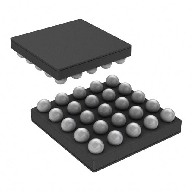
ICGOO在线商城 > 集成电路(IC) > 线性 - 音頻放大器 > LM48520TL/NOPB
- 型号: LM48520TL/NOPB
- 制造商: Texas Instruments
- 库位|库存: xxxx|xxxx
- 要求:
| 数量阶梯 | 香港交货 | 国内含税 |
| +xxxx | $xxxx | ¥xxxx |
查看当月历史价格
查看今年历史价格
LM48520TL/NOPB产品简介:
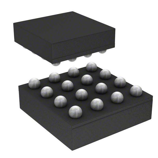
ICGOO电子元器件商城为您提供LM48520TL/NOPB由Texas Instruments设计生产,在icgoo商城现货销售,并且可以通过原厂、代理商等渠道进行代购。 LM48520TL/NOPB价格参考¥12.54-¥16.98。Texas InstrumentsLM48520TL/NOPB封装/规格:线性 - 音頻放大器, Amplifier IC 2-Channel (Stereo) Class D 25-DSBGA (2.46x2.46)。您可以下载LM48520TL/NOPB参考资料、Datasheet数据手册功能说明书,资料中有LM48520TL/NOPB 详细功能的应用电路图电压和使用方法及教程。
| 参数 | 数值 |
| 产品目录 | 集成电路 (IC)半导体 |
| 描述 | IC AMP AUDIO PWR 1.3W D 25DSBGA音频放大器 Boosted Stereo Class D Audio Pwr Amp w/ Output Speaker Protection & Spread Spectrum 25-DSBGA -40 to 85 |
| DevelopmentKit | LM48520TLBD |
| 产品分类 | |
| 品牌 | Texas Instruments |
| 产品手册 | |
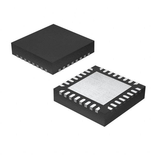
| 产品图片 |
|
| rohs | 符合RoHS无铅 / 符合限制有害物质指令(RoHS)规范要求 |
| 产品系列 | 音频 IC,音频放大器,Texas Instruments LM48520TL/NOPBBoomer® |
| 数据手册 | |
| 产品型号 | LM48520TL/NOPB |
| THD+噪声 | 0.04 % |
| 不同负载时的最大输出功率x通道数 | 1.3W x 2 @ 8 欧姆 |
| 产品 | Class-D |
| 产品目录页面 | |
| 产品种类 | 音频放大器 |
| 供应商器件封装 | 25-DSBGA (2.46x2.46) |
| 其它名称 | *LM48520TL/NOPB |
| 包装 | 剪切带 (CT) |
| 双重电源电压 | 3 V, 5 V |
| 商标 | Texas Instruments |
| 安装类型 | 表面贴装 |
| 安装风格 | SMD/SMT |
| 封装 | Reel |
| 封装/外壳 | 25-WFBGA, DSBGA |
| 封装/箱体 | DSBGA-25 |
| 工作温度 | -40°C ~ 85°C (TA) |
| 工作电源电压 | 2.7 V to 5 V |
| 工厂包装数量 | 250 |
| 最小工作温度 | - 40 C |
| 标准包装 | 1 |
| 特性 | 消除爆音,差分输入,短路保护,关机 |
| 电压-电源 | 2.4 V ~ 5.5 V |
| 电源电压-最大 | 5 V |
| 电源电压-最小 | 2.7 V |
| 电源电流 | 14.8 mA |
| 电源类型 | Triple |
| 类型 | D 类 |
| 系列 | LM48520 |
| 输入信号类型 | Differential |
| 输出功率 | 1.3 W |
| 输出类型 | 2 通道(立体声) |
| 音频负载电阻 | 8 Ohms |



- 商务部:美国ITC正式对集成电路等产品启动337调查
- 曝三星4nm工艺存在良率问题 高通将骁龙8 Gen1或转产台积电
- 太阳诱电将投资9.5亿元在常州建新厂生产MLCC 预计2023年完工
- 英特尔发布欧洲新工厂建设计划 深化IDM 2.0 战略
- 台积电先进制程称霸业界 有大客户加持明年业绩稳了
- 达到5530亿美元!SIA预计今年全球半导体销售额将创下新高
- 英特尔拟将自动驾驶子公司Mobileye上市 估值或超500亿美元
- 三星加码芯片和SET,合并消费电子和移动部门,撤换高东真等 CEO
- 三星电子宣布重大人事变动 还合并消费电子和移动部门
- 海关总署:前11个月进口集成电路产品价值2.52万亿元 增长14.8%


PDF Datasheet 数据手册内容提取
LM48520, LM48520TLBD www.ti.com SNAS367C–FEBRUARY2008–REVISEDAPRIL2013 LM48520 Boosted Stereo Class D Audio Power Amplifier with Output Speaker Protection and Spread Spectrum CheckforSamples:LM48520,LM48520TLBD FEATURES DESCRIPTION 1 • ClickandPopSuppression The LM48520 integrates a boost converter with a 2 high efficiency Class D stereo audio power amplifier • Low0.04μAShutdownCurrent to provide up to 1W/ch continuous power into an 8Ω • 78%Efficiency speaker when operating from 2.7V to 5.0V power • FilterlessClassD supply with boost voltage (PV1) of 5.0V. The LM48520 utilizes a proprietary spread spectrum pulse • 2.7V-5.0VOperation width modulation technique that lowers RF • 4AdjustableGainSettings interference and EMI levels. The Class D amplifier is • AdjustableOutputSwingLimiterwithSoft a low noise, filterless PWM architecture that Clipping eliminates the output filter, reducing external component count, board area, power consumption, • SpeakerProtection systemcost,andsimplifyingdesign. • ShortCircuitProtectiononAudioAmps The LM48520 is designed for use in mobile phones • IndependentBoostandAmplifierShutdown and other portable communication devices. The high Pins (78%) efficiency extends battery life when compared to Boosted Class AB amplifiers. The LM48520 APPLICATIONS features a low-power consumption shutdown mode. Shutdown may be enabled by driving the Shutdown • MobilePhones pin to a logic low (GND). Also, external leakage is • PDAs minimized via control of the ground reference via the • Portablemedia SW-OUTpin. • Cameras The LM48520 has 4 gain options which are pin • Handheldgames selectable via Gain0 and Gain1 pins. Output short circuit prevents the device from damage during fault KEY SPECIFICATIONS conditions. Superior click and pop suppression eliminates audible transients during power-up and • QuiescentPowerSupplyCurrent:11.5mA(typ) shutdown. • OutputPower(R =8Ω,THD+N ≤ 1%, L V =3.3V,PV1=5.0V):1.1W(typ) DD • ShutdownCurrent:0.04μA(typ) 1 Pleasebeawarethatanimportantnoticeconcerningavailability,standardwarranty,anduseincriticalapplicationsof TexasInstrumentssemiconductorproductsanddisclaimerstheretoappearsattheendofthisdatasheet. Alltrademarksarethepropertyoftheirrespectiveowners. 2 PRODUCTIONDATAinformationiscurrentasofpublicationdate. Copyright©2008–2013,TexasInstrumentsIncorporated Products conform to specifications per the terms of the Texas Instruments standard warranty. Production processing does not necessarilyincludetestingofallparameters.
LM48520, LM48520TLBD SNAS367C–FEBRUARY2008–REVISEDAPRIL2013 www.ti.com Typical Application L1 D1 V1 = VFB ( 1+ R1/R2) 6.8 PH Cs1 2.2 PF Cf1 R1 330 pF 40.2k Co 2.7V to 5.0V VDD SW 100 PF SW-GND BstFB R2 SS 16.2k 0.1 PF Cs FB-GND Boost SD Boost SD PV1 C4.s72 PF Amp SD Amp SD V1 Gain0 Gain0 Gain1 Gain1 GND Vlimit Vlimit 1 PF PGND INPUT R INR- Ci OUTR+ OUTR- 1 PF INR+ Ci 1 PF INPUT L INL- Ci OUTL+ 1 PF OUTL- INL+ Ci Figure1. TypicalLM48520AudioAmplifierApplicationCircuit Connection Diagram TopView 1 2 3 4 5 A VDD BstFB Soft SW_ SW Start GND B INR+ INR- FB_GND INL- INL+ C V1 BstSD GND Gain0 PV1 D AmpSD OUTR+ NC OUTL+ GAIN1 E VLimit OUTR- PGND OUTL- NC Figure2. DSBGAPackage SeePackageNumberYZR0025AAA 2 SubmitDocumentationFeedback Copyright©2008–2013,TexasInstrumentsIncorporated ProductFolderLinks:LM48520 LM48520TLBD
LM48520, LM48520TLBD www.ti.com SNAS367C–FEBRUARY2008–REVISEDAPRIL2013 PinDescriptions PinDesignator PinName PinFunction A1 VDD PowerSupply RegulatorFeedbackInput.ConnectBstFBtoanexternalresistivevoltagedividerto A2 BstFB settheboostoutputvoltage. A3 SoftStart Softstartcapacitor A4 SW_GND Boosterground A5 SW DrainoftheInternalFETswitch B1 INR+ Non-invertingrightchannelinput B2 INR- Invertingrightchannelinput B3 FB_GND GroundreturnforR1,R2resistordivider B4 INL- Invertingleftchannelinput B5 INL+ Non-invertingleftchannelinput C1 V1 Amplifiersupplyvoltage.ConnecttoPV1. C2 BstSD Regulatoractivelowshutdown C3 GND Ground C4 Gain0 Gainsettinginput0 C5 PV1 AmplifierH-bridgepowersupply.ConnecttoV1. D1 AmpSD Amplifieractivelowshutdown D2 OUTR+ Non-invertingrightchanneloutput D3 NC Noconnect D4 OUTL+ Non-invertingleftchanneloutput D5 Gain1 Gainsettinginput1 E1 VLimit Settocontroloutputclippinglevel E2 OUTR- Invertingrightchanneloutput E3 PGND Powerground E4 OUTL- Invertingleftchanneloutput E5 NC Noconnect Thesedeviceshavelimitedbuilt-inESDprotection.Theleadsshouldbeshortedtogetherorthedeviceplacedinconductivefoam duringstorageorhandlingtopreventelectrostaticdamagetotheMOSgates. Absolute Maximum Ratings (1)(2) SupplyVoltage(V ,V ) 6V DD 1 StorageTemperature −65°Cto+150°C InputVoltage −0.3VtoV +0.3V DD PowerDissipation (3) Internallylimited ESDSusceptibility (4) 2000V ESDSusceptibility (5) 200V JunctionTemperature 150°C ThermalResistanceθ (YZR0025AAA) 40.5°C/W JA (1) AbsoluteMaximumRatingsindicatelimitsbeyondwhichdamagetothedevicemayoccur.OperatingRatingsindicateconditionsfor whichthedeviceisfunctional,butdonotensurespecificperformancelimits.ElectricalCharacteristicsstateDCandACelectrical specificationsunderparticulartestconditionswhichensurespecificperformancelimits.Thisassumesthatthedeviceiswithinthe OperatingRatings.Specificationsarenotensuredforparameterswherenolimitisgiven,however,thetypicalvalueisagoodindication ofdeviceperformance. (2) IfMilitary/Aerospacespecifieddevicesarerequired,pleasecontacttheTexasInstrumentsSalesOffice/Distributorsforavailabilityand specifications. (3) ThemaximumpowerdissipationmustbederatedatelevatedtemperaturesandisdictatedbyT ,θ ,andtheambienttemperature, JMAX JA T .ThemaximumallowablepowerdissipationisP =(T −T )/θ orthegiveninAbsoluteMaximumRatings,whicheveris A DMAX JMAX A JA lower. (4) Humanbodymodel,100pFdischargedthrougha1.5kΩresistor. (5) MachineModel,220pF–240pFdischargedthroughallpins. Copyright©2008–2013,TexasInstrumentsIncorporated SubmitDocumentationFeedback 3 ProductFolderLinks:LM48520 LM48520TLBD
LM48520, LM48520TLBD SNAS367C–FEBRUARY2008–REVISEDAPRIL2013 www.ti.com Operating Ratings TemperatureRange T ≤T ≤T −40°C≤T ≤+85°C MIN A MAX A SupplyVoltage(V ) 2.7V≤V ≤5.0V DD DD AmplifierVoltage(V1) NotunderBoostedCondition 2.4V≤V ≤5.5V 1 AmplifierVoltage(PV1) UnderBoostedCondition 3.0V≤PV ≤5.0V 1 Electrical Characteristics V = 3.3V (1)(2) DD ThefollowingspecificationsapplyforV =3.3V,A =6dB,R =15µH+8Ω+15µH,f =1kHz,unlessotherwisespecified. DD V L IN LimitsapplyforT =25°C,R =40.2kΩ,R =16.2kΩ,V =PV =5V,V =GND.Allelectricalspecificationsareforamplifier A 1 2 1 1 limit andbooster. LM48520 Units Parameter TestConditions Typ Limit (Limits) (3) (4) (5) V =0,R =∞ IN LOAD V =2.7V 14.8 DD I QuiescentPowerSupplyCurrent DD V =3.3V 11.5 15.5 mA(max) DD V =5.0V 8.0 DD I ShutdownCurrent V =GND 0.04 1.0 μA(max) SD SHUTDOWN V ShutdownVoltageInputHigh ForSDBoost,SDAmp 1.4 V SDIH V ShutdownVoltageInputLow ForSDBoost,SDAmp 0.4 V SDIL T Wake-upTime Amplifier+BoosterWakeup 3 ms WU V OutputOffsetVoltage 5 mV OS G0,G1=GND 6 dB R =∞ L G0=V ,G1=GND DD 12 dB R =∞ L A Gain V G0=GND,G1=V DD 18 dB R =∞ L G0,G1=V DD 24 dB R =∞ L R =15μH+8Ω+15μH L THD+N=1%(max), 1.1 0.87 W(min) f=1kHz,22kHz,BW V =3.3V DD P OutputPower O R =15μH+8Ω+15μH L THD+N=10%(max), 1.3 W f=1kHz,22kHz,BW V =3.3V DD P =500mW,f=1kHz, O THD+N TotalHarmonicDistortion+Noise R =15μH+8Ω+15μH, 0.04 % L V =3.3V DD V =3.6V,f=20Hz–20kHz ε OutputNoise DD 32 µV OS InputstoACGND,Aweighted RMS (1) AllvoltagesaremeasuredwithrespecttotheGNDpin,unlessotherwisespecified. (2) AbsoluteMaximumRatingsindicatelimitsbeyondwhichdamagetothedevicemayoccur.OperatingRatingsindicateconditionsfor whichthedeviceisfunctional,butdonotensurespecificperformancelimits.ElectricalCharacteristicsstateDCandACelectrical specificationsunderparticulartestconditionswhichensurespecificperformancelimits.Thisassumesthatthedeviceiswithinthe OperatingRatings.Specificationsarenotensuredforparameterswherenolimitisgiven,however,thetypicalvalueisagoodindication ofdeviceperformance. (3) Typicalsaremeasuredat25°Candrepresenttheparametricnorm. (4) LimitsarespecifiedtoAOQL(AverageOutgoingQualityLevel). (5) Datasheetmin/maxspecificationlimitsareensuredbydesign,test,orstatisticalanalysis. 4 SubmitDocumentationFeedback Copyright©2008–2013,TexasInstrumentsIncorporated ProductFolderLinks:LM48520 LM48520TLBD
LM48520, LM48520TLBD www.ti.com SNAS367C–FEBRUARY2008–REVISEDAPRIL2013 Electrical Characteristics V = 3.3V (1)(2) (continued) DD ThefollowingspecificationsapplyforV =3.3V,A =6dB,R =15µH+8Ω+15µH,f =1kHz,unlessotherwisespecified. DD V L IN LimitsapplyforT =25°C,R =40.2kΩ,R =16.2kΩ,V =PV =5V,V =GND.Allelectricalspecificationsareforamplifier A 1 2 1 1 limit andbooster. LM48520 Units Parameter TestConditions Typ Limit (Limits) (3) (4) (5) V =200mV Sine, RIPPLE P-P 82 dB f =217Hz RIPPLE= PSRR PowerSupplyRejectionRatio V =200mV Sine, RIPPLE P-P 79 dB f =1kHz RIPPLE= CMRR CommonModeRejectionRatio V =1V ,f =217Hz 67 dB RIPPLE P-P RIPPLE P =1W,f=1kHz, O R =15μH+8Ω+15μH η Efficiency L 78 % V =3.3V DD V =4.2V DD V FeedbackPinReferenceVoltage See (6) 1.24 V FB OutputVoltageinclippedstatewith V =2V,R =8Ω,V =2V 1.9 Vpk(min) V limit L IN P 2.5 outclipped softclipactivated V =8/3(PV1–2V ) 3.2 Vpk(max) outclipped limit (6) FeedbackpinreferencevoltageismeasuredwiththeAudioAmplifierdisconnectedfromtheBoostconverter(theBoostconverteris unloaded). Copyright©2008–2013,TexasInstrumentsIncorporated SubmitDocumentationFeedback 5 ProductFolderLinks:LM48520 LM48520TLBD
LM48520, LM48520TLBD SNAS367C–FEBRUARY2008–REVISEDAPRIL2013 www.ti.com Typical Performance Characteristics THD+NvsFrequency THD+NvsFrequency V =2.7V,P =800mW,R =8Ω V =3.3V,P =900mW,R =8Ω DD OUT L DD OUT L 100 100 10 10 %) 1 %) 1 N ( N ( + + D D H 0.1 H 0.1 T T 0.01 0.01 0.001 0.001 20 100 1k 10k20k 20 100 1k 10k20k FREQUENCY (Hz) FREQUENCY (Hz) Figure3. Figure4. THD+NvsFrequency THD+NvsOutputPower V =5.0V,P =1W,R =8Ω V =2.7V,R =8Ω DD OUT L DD L 100 100 10 10 %) 1 %) 1 N ( N ( + + D D H 0.1 H 0.1 T T 0.01 0.01 0.001 0.001 20 100 1k 10k20k 10m 100m 1 2 FREQUENCY (Hz) OUTPUT POWER (W) Figure5. Figure6. THD+NvsOutputPower THD+NvsOutputPower V =3.3V,R =8Ω V =5.0V,R =8Ω DD L DD L 100 100 10 10 %) 1 %) 1 N ( N ( + + D D H 0.1 H 0.1 T T 0.01 0.01 0.001 0.001 10m 100m 1 2 10m 100m 1 2 OUTPUT POWER (W) OUTPUT POWER (W) Figure7. Figure8. 6 SubmitDocumentationFeedback Copyright©2008–2013,TexasInstrumentsIncorporated ProductFolderLinks:LM48520 LM48520TLBD
LM48520, LM48520TLBD www.ti.com SNAS367C–FEBRUARY2008–REVISEDAPRIL2013 Typical Performance Characteristics (continued) PowerDissipationvsOutputPower PowerDissipationvsOutputPower V =2.7V,R =8Ω,f=1kHz V =3.3V,R =8Ω,f=1kHz DD L DD L 800 750 700 W) 600 mW) 600 N (m ON ( 500 TIO 450 ATI A P 400 P SI SI S DIS 300 R DI 300 R E E W 200 W O O 150 P P 100 POUT = POUTL + POUTR POUT = POUTL + POUTR 0 0 0 500 1000 1500 2000 2500 3000 0 500 1000 1500 2000 2500 OUTPUT POWER (mW) OUTPUT POWER (mW) Figure9. Figure10. PowerDissipationvsOutputPower EfficiencyvsOutputPower V =5.0V,R =8Ω,f=1kHz V =2.7V,R =8Ω,f=1kHz DD L DD L 800 100 90 700 W) 80 N (m 600 %) 70 R DISSIPATIO 345000000 EFFICIENCY ( 34560000 E W 200 O 20 P 100 10 POUT = POUTL + POUTR 0 00 500 1000 1500 2000 2500 0 500 1000 1500 2000 2500 30003500 OUTPUT POWER (mW) OUTPUT POWER (mW) Figure11. Figure12. EfficiencyvsOutputPower EfficiencyvsOutputPower V =3.3V,R =8Ω,f=1kHz V =5.0V,R =8Ω,f=1kHz DD L DD L 100 100 90 90 80 80 70 70 %) %) Y ( 60 Y ( 60 C C N 50 N 50 E E CI CI FI 40 FI 40 F F E 30 E 30 20 20 10 10 0 0 0 500 1000 1500 2000 2500 3000 0 500 1000 1500 2000 2500 OUTPUT POWER (mW) OUTPUT POWER (mW) Figure13. Figure14. Copyright©2008–2013,TexasInstrumentsIncorporated SubmitDocumentationFeedback 7 ProductFolderLinks:LM48520 LM48520TLBD
LM48520, LM48520TLBD SNAS367C–FEBRUARY2008–REVISEDAPRIL2013 www.ti.com Typical Performance Characteristics (continued) CMRRvsFrequency PSRRvsFrequency V =3.3V,V =1V ,R =8Ω V =3.3V,V =200mV ,R =8Ω DD RIPPLE P-P L DD RIPPLE P-P L 0 0 -10 -10 -20 -20 -30 -30 B) B) -40 MRR (d --5400 SRR (d -50 C P -60 -60 -70 -70 -80 -80 -90 -90 -100 10 100 1000 10000 100000 10 100 1000 10000 100000 FREQUENCY (Hz) FREQUENCY (Hz) Figure15. Figure16. SupplyCurrentvsSupplyVoltage OutputPowervsSupplyVoltage NoLoad R =8Ω,f=1kHz L 4 16 14 THD+N = 10% A) 12 W) 3 ENT (m 10 WER ( R O 2 UR 8 T P THD+N = 1% C U PLY 6 UTP P O 1 U 4 S 2 0 0 2 2.5 3 3.5 4 4.5 5 5.5 2 2.5 3 3.5 4 4.5 5 5.5 SUPPLY VOLTAGE (V) SUPPLY VOLTAGE (V) Figure17. Figure18. BoostOutputVoltagevsLoadCurrent BoostOutputVoltagevsLoadCurrent V =2.7V V =3.3V DD DD 5.4 5.4 V) 5.2 V) E ( E ( 5.2 AG 5 AG T T L L O O 5 V 4.8 V T T U U TP 4.6 TP U U 4.8 O O ST 4.4 ST O O O O 4.6 B 4.2 B 4 4.4 0 200 400 600 800 10001200 1400 0 200 400 600 800 10001200 1400 LOAD CURRENT (mA) LOAD CURRENT (mA) Figure19. Figure20. 8 SubmitDocumentationFeedback Copyright©2008–2013,TexasInstrumentsIncorporated ProductFolderLinks:LM48520 LM48520TLBD
LM48520, LM48520TLBD www.ti.com SNAS367C–FEBRUARY2008–REVISEDAPRIL2013 Typical Performance Characteristics (continued) BoostOutputVoltagevsLoadCurrent V =5.0V DD 5.4 V) E ( G 5.3 A T L O V T U 5.2 P T U O T OS 5.1 O B 5 0 200 400 600 800 10001200 1400 LOAD CURRENT (mA) Figure21. Copyright©2008–2013,TexasInstrumentsIncorporated SubmitDocumentationFeedback 9 ProductFolderLinks:LM48520 LM48520TLBD
LM48520, LM48520TLBD SNAS367C–FEBRUARY2008–REVISEDAPRIL2013 www.ti.com APPLICATION INFORMATION General Amplifier Function The LM48520 features a Class D audio power amplifier that utilizes a filterless modulation scheme, reducing external component count, conserving board space and reducing system cost. The outputs of the device transition from PV1 to GND with a 300kHz switching frequency. With no signal applied, the outputs (V and LS+ V ) switch with a 50% duty cycle, in phase, causing the two outputs to cancel. This cancellation results in no LS- netvoltageacrossthespeaker,thusthereisnocurrenttotheloadintheidlestate. Withtheinputsignalapplied,thedutycycle(pulsewidth)oftheLM48520outputschanges.Forincreasingoutput voltage, the duty cycle of V increases, while the duty cycle of V decreases. For decreasing output voltages, LS+ LS- theconverseoccurs.Thedifferencebetweenthetwopulsewidthsyieldsthedifferentialoutputvoltage. Differential Amplifier Explanation The amplifier portion of the LM48520 is a fully differential amplifier that features differential input and output stages. A differential amplifier amplifies the difference between the two input signals. Traditional audio power amplifiers have typically offered only single-ended inputs resulting in a 6dB reduction in signal to noise ratio relative to differential inputs. The amplifier also offers the possibility of DC input coupling which eliminates the two external AC coupling, DC blocking capacitors. The amplifier can be used, however, as a single ended input amplifier while still retaining it's fully differential benefits. In fact, completely unrelated signals may be placed on the input pins. The amplifier portion of the LM48520 simply amplifies the difference between the signals. A major benefit of a differential amplifier is the improved common mode rejection ratio (CMRR) over single input amplifiers. The common-mode rejection characteristic of the differential amplifier reduces sensitivity to ground offsetrelatednoiseinjection,especiallyimportantinhighnoiseapplications. Amplifier Dissipation and Efficiency The major benefit of a Class D amplifier is increased efficiency versus a Class AB. The efficiency of the LM48520 is attributed to the region of operation of the transistors in the output stage. The Class D output stage acts as current steering switches, consuming negligible amounts of power compared to their Class AB counterparts. Most of the power loss associated with the output stage is due to the IR loss of the MOSFET on- resistance,alongwithswitchinglossesduetogatecharge. Regulator Power Dissipation At higher duty cycles, the increased ON-time of the switch FET means the maximum output current will be determined by power dissipation within the LM48520 FET switch. The switch power dissipation from ON-time conductioniscalculatedby: P =DCx(I )2xR (W) (1) D(SWITCH) INDUCTOR(AVE) DS(ON) where: WhereDCisthedutycycle Shutdown Function The LM48520 features independent amplifier and regulator shutdown controls, allowing each portion of the device to be disabled or enabled independently. AmpSD controls the Class D amplifiers, while BstSD controls the regulator. Driving either inputs low disables the corresponding portion of the device, and reducing supply current. When the regulator is disabled, both FB_GND switches open, further reducing shutdown current by eliminating the current path to GND through the regulator feedback network. With the regulator disabled, there is still a current path from V , through the inductor and diode, to the amplifier power supply. This allows the amplifier to DD operateevenwhentheregulatorisdisabled.ThevoltageatPV1andV1willbe: V —[V +(I xDCR)] (2) DD D L where: V istheforwardvoltageoftheSchottkydiode D I isthecurrentthroughtheinductor L 10 SubmitDocumentationFeedback Copyright©2008–2013,TexasInstrumentsIncorporated ProductFolderLinks:LM48520 LM48520TLBD
LM48520, LM48520TLBD www.ti.com SNAS367C–FEBRUARY2008–REVISEDAPRIL2013 DCRistheDCresistanceoftheinductor Additionally,whentheregulatorisdisabled,anexternalvoltagebetween2.4Vand5.5Vcanbeapplieddirectlyto PV1andV1topowertheamplifier. It is best to switch between ground and V for minimum current consumption while in shutdown. The LM48520 DD may be disabled with shutdown voltages in between GND and V , the idle current will be greater than the DD typical 0.1µA value. Increased THD+N may also be observed when a voltage of less than V is applied to DD AmpSD. Proper Selection of External Components Proper selection of external components in applications using integrated power amplifiers, and switching DC-DC converters, is critical for optimizing device and system performance. Consideration to component values must be usedtomaximizeoverallsystemquality. The best capacitors for use with the switching converter portion of the LM48520 are multi-layer ceramic capacitors. They have the lowest ESR (equivalent series resistance) and highest resonance frequency, which makesthemoptimumforhighfrequencyswitchingconverters. When selecting a ceramic capacitor, only X5R and X7R dielectric types should be used. Other types such as Z5U and Y5F have such severe loss of capacitance due to effects of temperature variation and applied voltage, they may provide as little as 20% of rated capacitance in many typical applications. Always consult capacitor manufacturer’s data curves before selecting a capacitor. High-quality ceramic capacitors can be obtained from Taiyo-Yuden,AVX,andMurata. Power Supply Bypassing for Amplifier As with any amplifier, proper supply bypassing is critical for low noise performance and high power supply rejection.ThecapacitorlocationonbothPV1,V1andV pinsshouldbeasclosetothedeviceaspossible. DD Selecting Input Capacitor for Audio Amplifier Input capacitors, C , in conjunction with the input impedance of the LM48520 forms a high pass filter that IN removes the DC bias from an incoming signal. The AC-coupling capacitor allows the amplifier to bias the signal toanoptimalDClevel.Assumingzerosourceimpedance,the-3dBpointofthehighpassfilterisgivenby: f =1/2πR C (3) (–3dB) IN IN Choose C such that f is well below that lowest frequency of interest. Setting f too high affects the low- IN -3dB -3dB frequency responses of the amplifier. Use capacitors with low voltage coefficient dielectrics, such as tantalum or aluminum electrolytic. Capacitors with high-voltage coefficients, such as ceramics, may result in increased distortion at low frequencies. Other factors to consider when designing the input filter include the constraints of the overall system. Although high fidelity audio requires a flat frequency response between 20Hz and 20kHz, portable devices such as cell phones may only concentrate on the frequency range of the frequency range of the spoken human voice (typically 300Hz to 4kHz). In addition, the physical size of the speakers used in such portabledeviceslimitsthelowfrequencyresponse;inthiscase,frequenciesbelow150Hzmaybefilteredout. Selecting Output Capacitor (C ) for Boost Converter O A single 100µF low ESR tantalum capacitor provides sufficient output capacitance for most applications. Higher capacitor values improve line regulation and transient response. Typical electrolytic capacitors are not suitable for switching converters that operate above 500kHz because of significant ringing and temperature rise due to self-heating from ripple current. An output capacitor with excessive ESR reduces phase margin and causes instability. Selecting Input Capacitor (Cs1) for Boost Converter An input capacitor is required to serve as an energy reservoir for the current which must flow into the coil each time the switch turns ON. This capacitor must have extremely low ESR, so ceramic is the best choice. We recommend a nominal value of 2.2µF, but larger values can be used. Since this capacitor reduces the amount of voltage ripple seen at the input pin, it also reduces the amount of EMI passed back along that line to other circuitry. Copyright©2008–2013,TexasInstrumentsIncorporated SubmitDocumentationFeedback 11 ProductFolderLinks:LM48520 LM48520TLBD
LM48520, LM48520TLBD SNAS367C–FEBRUARY2008–REVISEDAPRIL2013 www.ti.com Selecting Soft-Start (C ) Capacitor SS The soft-start function charges the boost converter reference voltage slowly. This allows the output of the boost converter to ramp up slowly thus limiting the transient current at startup. Selecting a soft-start capacitor (C ) SS value presents a trade off between the wake-up time and the startup transient current. Using a larger capacitor value will increase wake-up time and decrease startup transient current while the apposite effect happens with a smaller capacitor value. A general guideline is to use a capacitor value 1000 times smaller than the output capacitanceoftheboostconverter(C ).A0.1uFsoft-startcapacitorisrecommendedforatypicalapplication. O Setting the Output Voltage (V ) of boost Converter 1 The output voltage is set using the external resistors R1 and R2 (see Figure 1). A value of approximately 13.3kΩ isrecommendedforR2toestablishadividercurrentofapproximately92µA.R1iscalculatedusingtheformula: R1=R2X(V /1.23−1) (4) 1 Feed-Forward Compensation for Boost Converter Although the LM48520's internal Boost converter is internally compensated, the external feed-forward capacitor C is required for stability (see Figure 1). Adding this capacitor puts a zero in the loop response of the converter. f The recommended frequency for the zero fz should be approximately 6kHz. C1 can be calculated using the f formula: C =1/(2XR1Xfz) (5) f Selecting Diodes for Boost The external diode used in Figure 1 should be a Schottky diode. A 20V diode such as the MBRS320T3 is recommended. TheMBRS320T3seriesofdiodesaredesignedtohandleamaximumaveragecurrentof3A. Duty Cycle The maximum duty cycle of the boost converter determines the maximum boost ratio of output-to-input voltage that the converter can attain in continuous mode of operation. The duty cycle for a given boost application is definedas: DutyCycle=V +V -V /V +V -V (6) OUT DIODE IN OUT DIODE SW Thisappliesforcontinuousmodeoperation. Selecting Inductor Value Inductor value involves trade-offs in performance. Larger inductors reduce inductor ripple current, which typically means less output voltage ripple (for a given size of output capacitor). Larger inductors also mean more load powercanbedeliveredbecausetheenergystoredduringeachswitchingcycleis: E=L/2X(I )2 (7) P Where “lp” is the peak inductor current. The LM48520 will limit its switch current based on peak current. With I P fixed, increasing L will increase the maximum amount of power available to the load. Conversely, using too little inductancemaylimittheamountofloadcurrentwhichcanbedrawnfromtheoutput.Bestperformanceisusually obtained when the converter is operated in “continuous” mode at the load current range of interest, typically giving better load regulation and less output ripple. Continuous operation is defined as not allowing the inductor current to drop to zero during the cycle. Boost converters shift over to discontinuous operation if the load is reducedfarenough,butalargerinductorstayscontinuousoverawiderloadcurrentrange. During the TBDµs ON-time, the inductor current ramps up TBDA and ramps down an equal amount during the OFF-time. This is defined as the inductor “ripple current”. It can also be seen that if the load current drops to about TBDmA, the inductor current will begin touching the zero axis which means it will be in discontinuous mode. A similar analysis can be performed on any boost converter, to make sure the ripple current is reasonable andcontinuousoperationwillbemaintainedatthetypicalloadcurrentvalues. 12 SubmitDocumentationFeedback Copyright©2008–2013,TexasInstrumentsIncorporated ProductFolderLinks:LM48520 LM48520TLBD
LM48520, LM48520TLBD www.ti.com SNAS367C–FEBRUARY2008–REVISEDAPRIL2013 Maximum Switch Current The maximum FET switch current available before the current limiter cuts in is dependent on duty cycle of the application. This is illustrated in a graph in the Typical Performance Characteristics section which shows typical valuesofswitchcurrentasafunctionofeffective(actual)dutycycle. Calculating Output Current of Boost Converter (I ) AMP Theloadcurrentisrelatedtotheaverageinductorcurrentbytherelation: I =I (AVG)x(1-DC) (8) LOAD IND where: "DC"isthedutycycleoftheapplication Theswitchcurrentcanbefoundby: I =I (AVG)+1/2(I ) (9) SW IND RIPPLE Inductorripplecurrentisdependentoninductance,dutycycle,inputvoltageandfrequency: I =DCx(V -V )/(fxL) (10) RIPPLE IN SW combining all terms, we can develop an expression which allows the maximum available load current to be calculated: I (max)=(1–DC)x(I (max)–DC(V -V ))/fL (11) LOAD SW IN SW The equation shown to calculate maximum load current takes into account the losses in the inductor or turn-OFF switchinglossesoftheFETanddiode. Design Parameters V and I SW SW The value of the FET "ON" voltage (referred to as V in Equation 4 thru Equation 9) is dependent on load SW current. A good approximation can be obtained by multiplying the "ON Resistance" of the FET times the average inductorcurrent. FET on resistance increases at V values below 5V, since the internal N-FET has less gate voltage in this input IN voltage range (see Typical Performance Characteristics curves). Above V = 5V, the FET gate voltage is IN internallyclampedto5V. The maximum peak switch current the device can deliver is dependent on duty cycle. For higher duty cycles, see TypicalPerformanceCharacteristicscurves. Inductor Suppliers The recommended inductor for the LM48520 is the NR8040T6R8N from Taiyo Yuden. When selecting an inductor, make certain that the continuous current rating is high enough to avoid saturation at peak currents, where: I =(PV1/V )xI (12) IND DD LOAD(BOOST) A suitable core type must be used to minimize core (switching) losses, and wire power losses must be consideredwhenselectingthecurrentrating. PCB Layout Guidelines High frequency boost converters require very careful layout of components in order to get stable operation and lownoise. All components must be as close as possible to the LM48520 device. It is recommended that a four layer PCB beusedsothatinternalgroundplanesareavailable. Someadditionalguidelinestobeobserved(alldesignatorsarereferencingFigure1): 1. Keep the path between L1, D1, and Co extremely short. Parasitic trace inductance in series with D1 and Co willincreasenoiseandringing. 2. The feedback components R1, R2 and Cf1 must be kept close to the FB pin to prevent noise injection on the FBpintrace. 3. Since the external components of the boost converter are switching, L1 and D1 should be kept away from Copyright©2008–2013,TexasInstrumentsIncorporated SubmitDocumentationFeedback 13 ProductFolderLinks:LM48520 LM48520TLBD
LM48520, LM48520TLBD SNAS367C–FEBRUARY2008–REVISEDAPRIL2013 www.ti.com theinputtracestopreventthenoisefrominjectingintotheinput. 4. The power supply bypass capacitors, Cs1 and Cs2 should be placed as close to the LM48520 device as possible. GROUNDINGGUIDELINES There are three grounds on the LM48520, GND, SW_GND, and PGND. When laying out the PCB, it is critical to connect the grounds as close to the device as possible. The simplest way to do that is to place vias close to the GND, SW_GND, and PGND bumps and connect the GND, SW_GND, and PGND vias using a single ground planeinaninnerlayerofthePCB. Output Speaker Protection Function The LM48520’s output voltage limiter can be used to set a minimum and maximum output voltage swing magnitude. The voltage applied to the VLimit pin controls the limit on the output voltage level. The output level is determinedbythefollowingequation: Voutclipped=8/3*(PV1—2*Vlimit) (13) where: Voutclipped=thedesiredoutputlevelmeasuredinVpk PV1=Boostoutputvoltage VlimitisthevoltageappliedthetheVlimitpinontheLM48520 or Voutclipped=1/2*(PV1—3/8*Voutclipped) (14) Todisablethelimiter,setVlimit=0V. Figure 22 provides an example of how the output voltage limiter functions with V = 3.3V, A = 6dB, PV1 = 5V, DD V Vlimit=2V,R =8Ω,V =2V . L IN P 4 No Clipping 3 2 With Soft Clipping V) 1 T ( U 0 P T U O -1 -2 -3 -4 200 Ps Figure22. SoftClippingvsNoClipping Revision History Rev Date Description 1.0 02/27/08 Initialrelease. 1.01 03/07/08 AddedtheSoftclippingvsNoclippingcurve. 1.02 03/12/08 Textedits. C 04/05/13 ChangedlayoutofNationalDataSheettoTIformat. 14 SubmitDocumentationFeedback Copyright©2008–2013,TexasInstrumentsIncorporated ProductFolderLinks:LM48520 LM48520TLBD
PACKAGE OPTION ADDENDUM www.ti.com 24-Sep-2015 PACKAGING INFORMATION Orderable Device Status Package Type Package Pins Package Eco Plan Lead/Ball Finish MSL Peak Temp Op Temp (°C) Device Marking Samples (1) Drawing Qty (2) (6) (3) (4/5) LM48520TL/NOPB ACTIVE DSBGA YZR 25 250 Green (RoHS SNAGCU Level-1-260C-UNLIM -40 to 85 GI5 & no Sb/Br) (1) The marketing status values are defined as follows: ACTIVE: Product device recommended for new designs. LIFEBUY: TI has announced that the device will be discontinued, and a lifetime-buy period is in effect. NRND: Not recommended for new designs. Device is in production to support existing customers, but TI does not recommend using this part in a new design. PREVIEW: Device has been announced but is not in production. Samples may or may not be available. OBSOLETE: TI has discontinued the production of the device. (2) Eco Plan - The planned eco-friendly classification: Pb-Free (RoHS), Pb-Free (RoHS Exempt), or Green (RoHS & no Sb/Br) - please check http://www.ti.com/productcontent for the latest availability information and additional product content details. TBD: The Pb-Free/Green conversion plan has not been defined. Pb-Free (RoHS): TI's terms "Lead-Free" or "Pb-Free" mean semiconductor products that are compatible with the current RoHS requirements for all 6 substances, including the requirement that lead not exceed 0.1% by weight in homogeneous materials. Where designed to be soldered at high temperatures, TI Pb-Free products are suitable for use in specified lead-free processes. Pb-Free (RoHS Exempt): This component has a RoHS exemption for either 1) lead-based flip-chip solder bumps used between the die and package, or 2) lead-based die adhesive used between the die and leadframe. The component is otherwise considered Pb-Free (RoHS compatible) as defined above. Green (RoHS & no Sb/Br): TI defines "Green" to mean Pb-Free (RoHS compatible), and free of Bromine (Br) and Antimony (Sb) based flame retardants (Br or Sb do not exceed 0.1% by weight in homogeneous material) (3) MSL, Peak Temp. - The Moisture Sensitivity Level rating according to the JEDEC industry standard classifications, and peak solder temperature. (4) There may be additional marking, which relates to the logo, the lot trace code information, or the environmental category on the device. (5) Multiple Device Markings will be inside parentheses. Only one Device Marking contained in parentheses and separated by a "~" will appear on a device. If a line is indented then it is a continuation of the previous line and the two combined represent the entire Device Marking for that device. (6) Lead/Ball Finish - Orderable Devices may have multiple material finish options. Finish options are separated by a vertical ruled line. Lead/Ball Finish values may wrap to two lines if the finish value exceeds the maximum column width. Important Information and Disclaimer:The information provided on this page represents TI's knowledge and belief as of the date that it is provided. TI bases its knowledge and belief on information provided by third parties, and makes no representation or warranty as to the accuracy of such information. Efforts are underway to better integrate information from third parties. TI has taken and continues to take reasonable steps to provide representative and accurate information but may not have conducted destructive testing or chemical analysis on incoming materials and chemicals. TI and TI suppliers consider certain information to be proprietary, and thus CAS numbers and other limited information may not be available for release. In no event shall TI's liability arising out of such information exceed the total purchase price of the TI part(s) at issue in this document sold by TI to Customer on an annual basis. Addendum-Page 1
PACKAGE OPTION ADDENDUM www.ti.com 24-Sep-2015 Addendum-Page 2
PACKAGE MATERIALS INFORMATION www.ti.com 2-Sep-2015 TAPE AND REEL INFORMATION *Alldimensionsarenominal Device Package Package Pins SPQ Reel Reel A0 B0 K0 P1 W Pin1 Type Drawing Diameter Width (mm) (mm) (mm) (mm) (mm) Quadrant (mm) W1(mm) LM48520TL/NOPB DSBGA YZR 25 250 178.0 8.4 2.69 2.69 0.76 4.0 8.0 Q1 PackMaterials-Page1
PACKAGE MATERIALS INFORMATION www.ti.com 2-Sep-2015 *Alldimensionsarenominal Device PackageType PackageDrawing Pins SPQ Length(mm) Width(mm) Height(mm) LM48520TL/NOPB DSBGA YZR 25 250 210.0 185.0 35.0 PackMaterials-Page2
MECHANICAL DATA YZR0025xxx 0.600±0.075 D E TLA25XXX (Rev D) D: Max = 2.511 mm, Min =2 .451 mm E: Max = 2.511 mm, Min =2 .451 mm 4215055/A 12/12 NOTES: A.Alllineardimensionsareinmillimeters.DimensioningandtolerancingperASMEY14.5M-1994. B.Thisdrawingissubjecttochangewithoutnotice. www.ti.com
IMPORTANTNOTICE TexasInstrumentsIncorporated(TI)reservestherighttomakecorrections,enhancements,improvementsandotherchangestoits semiconductorproductsandservicesperJESD46,latestissue,andtodiscontinueanyproductorserviceperJESD48,latestissue.Buyers shouldobtainthelatestrelevantinformationbeforeplacingordersandshouldverifythatsuchinformationiscurrentandcomplete. TI’spublishedtermsofsaleforsemiconductorproducts(http://www.ti.com/sc/docs/stdterms.htm)applytothesaleofpackagedintegrated circuitproductsthatTIhasqualifiedandreleasedtomarket.AdditionaltermsmayapplytotheuseorsaleofothertypesofTIproductsand services. ReproductionofsignificantportionsofTIinformationinTIdatasheetsispermissibleonlyifreproductioniswithoutalterationandis accompaniedbyallassociatedwarranties,conditions,limitations,andnotices.TIisnotresponsibleorliableforsuchreproduced documentation.Informationofthirdpartiesmaybesubjecttoadditionalrestrictions.ResaleofTIproductsorserviceswithstatements differentfromorbeyondtheparametersstatedbyTIforthatproductorservicevoidsallexpressandanyimpliedwarrantiesforthe associatedTIproductorserviceandisanunfairanddeceptivebusinesspractice.TIisnotresponsibleorliableforanysuchstatements. BuyersandotherswhoaredevelopingsystemsthatincorporateTIproducts(collectively,“Designers”)understandandagreethatDesigners remainresponsibleforusingtheirindependentanalysis,evaluationandjudgmentindesigningtheirapplicationsandthatDesignershave fullandexclusiveresponsibilitytoassurethesafetyofDesigners'applicationsandcomplianceoftheirapplications(andofallTIproducts usedinorforDesigners’applications)withallapplicableregulations,lawsandotherapplicablerequirements.Designerrepresentsthat,with respecttotheirapplications,Designerhasallthenecessaryexpertisetocreateandimplementsafeguardsthat(1)anticipatedangerous consequencesoffailures,(2)monitorfailuresandtheirconsequences,and(3)lessenthelikelihoodoffailuresthatmightcauseharmand takeappropriateactions.DesigneragreesthatpriortousingordistributinganyapplicationsthatincludeTIproducts,Designerwill thoroughlytestsuchapplicationsandthefunctionalityofsuchTIproductsasusedinsuchapplications. TI’sprovisionoftechnical,applicationorotherdesignadvice,qualitycharacterization,reliabilitydataorotherservicesorinformation, including,butnotlimitedto,referencedesignsandmaterialsrelatingtoevaluationmodules,(collectively,“TIResources”)areintendedto assistdesignerswhoaredevelopingapplicationsthatincorporateTIproducts;bydownloading,accessingorusingTIResourcesinany way,Designer(individuallyor,ifDesignerisactingonbehalfofacompany,Designer’scompany)agreestouseanyparticularTIResource solelyforthispurposeandsubjecttothetermsofthisNotice. TI’sprovisionofTIResourcesdoesnotexpandorotherwisealterTI’sapplicablepublishedwarrantiesorwarrantydisclaimersforTI products,andnoadditionalobligationsorliabilitiesarisefromTIprovidingsuchTIResources.TIreservestherighttomakecorrections, enhancements,improvementsandotherchangestoitsTIResources.TIhasnotconductedanytestingotherthanthatspecifically describedinthepublisheddocumentationforaparticularTIResource. Designerisauthorizedtouse,copyandmodifyanyindividualTIResourceonlyinconnectionwiththedevelopmentofapplicationsthat includetheTIproduct(s)identifiedinsuchTIResource.NOOTHERLICENSE,EXPRESSORIMPLIED,BYESTOPPELOROTHERWISE TOANYOTHERTIINTELLECTUALPROPERTYRIGHT,ANDNOLICENSETOANYTECHNOLOGYORINTELLECTUALPROPERTY RIGHTOFTIORANYTHIRDPARTYISGRANTEDHEREIN,includingbutnotlimitedtoanypatentright,copyright,maskworkright,or otherintellectualpropertyrightrelatingtoanycombination,machine,orprocessinwhichTIproductsorservicesareused.Information regardingorreferencingthird-partyproductsorservicesdoesnotconstitutealicensetousesuchproductsorservices,orawarrantyor endorsementthereof.UseofTIResourcesmayrequirealicensefromathirdpartyunderthepatentsorotherintellectualpropertyofthe thirdparty,oralicensefromTIunderthepatentsorotherintellectualpropertyofTI. TIRESOURCESAREPROVIDED“ASIS”ANDWITHALLFAULTS.TIDISCLAIMSALLOTHERWARRANTIESOR REPRESENTATIONS,EXPRESSORIMPLIED,REGARDINGRESOURCESORUSETHEREOF,INCLUDINGBUTNOTLIMITEDTO ACCURACYORCOMPLETENESS,TITLE,ANYEPIDEMICFAILUREWARRANTYANDANYIMPLIEDWARRANTIESOF MERCHANTABILITY,FITNESSFORAPARTICULARPURPOSE,ANDNON-INFRINGEMENTOFANYTHIRDPARTYINTELLECTUAL PROPERTYRIGHTS.TISHALLNOTBELIABLEFORANDSHALLNOTDEFENDORINDEMNIFYDESIGNERAGAINSTANYCLAIM, INCLUDINGBUTNOTLIMITEDTOANYINFRINGEMENTCLAIMTHATRELATESTOORISBASEDONANYCOMBINATIONOF PRODUCTSEVENIFDESCRIBEDINTIRESOURCESOROTHERWISE.INNOEVENTSHALLTIBELIABLEFORANYACTUAL, DIRECT,SPECIAL,COLLATERAL,INDIRECT,PUNITIVE,INCIDENTAL,CONSEQUENTIALOREXEMPLARYDAMAGESIN CONNECTIONWITHORARISINGOUTOFTIRESOURCESORUSETHEREOF,ANDREGARDLESSOFWHETHERTIHASBEEN ADVISEDOFTHEPOSSIBILITYOFSUCHDAMAGES. UnlessTIhasexplicitlydesignatedanindividualproductasmeetingtherequirementsofaparticularindustrystandard(e.g.,ISO/TS16949 andISO26262),TIisnotresponsibleforanyfailuretomeetsuchindustrystandardrequirements. WhereTIspecificallypromotesproductsasfacilitatingfunctionalsafetyorascompliantwithindustryfunctionalsafetystandards,such productsareintendedtohelpenablecustomerstodesignandcreatetheirownapplicationsthatmeetapplicablefunctionalsafetystandards andrequirements.Usingproductsinanapplicationdoesnotbyitselfestablishanysafetyfeaturesintheapplication.Designersmust ensurecompliancewithsafety-relatedrequirementsandstandardsapplicabletotheirapplications.DesignermaynotuseanyTIproductsin life-criticalmedicalequipmentunlessauthorizedofficersofthepartieshaveexecutedaspecialcontractspecificallygoverningsuchuse. Life-criticalmedicalequipmentismedicalequipmentwherefailureofsuchequipmentwouldcauseseriousbodilyinjuryordeath(e.g.,life support,pacemakers,defibrillators,heartpumps,neurostimulators,andimplantables).Suchequipmentincludes,withoutlimitation,all medicaldevicesidentifiedbytheU.S.FoodandDrugAdministrationasClassIIIdevicesandequivalentclassificationsoutsidetheU.S. TImayexpresslydesignatecertainproductsascompletingaparticularqualification(e.g.,Q100,MilitaryGrade,orEnhancedProduct). Designersagreethatithasthenecessaryexpertisetoselecttheproductwiththeappropriatequalificationdesignationfortheirapplications andthatproperproductselectionisatDesigners’ownrisk.Designersaresolelyresponsibleforcompliancewithalllegalandregulatory requirementsinconnectionwithsuchselection. DesignerwillfullyindemnifyTIanditsrepresentativesagainstanydamages,costs,losses,and/orliabilitiesarisingoutofDesigner’snon- compliancewiththetermsandprovisionsofthisNotice. MailingAddress:TexasInstruments,PostOfficeBox655303,Dallas,Texas75265 Copyright©2017,TexasInstrumentsIncorporated

 Datasheet下载
