ICGOO在线商城 > 开发板,套件,编程器 > 评估板 - 音频放大器 > LM4673TMBD
 Datasheet下载
- 型号: LM4673TMBD
- 制造商: Texas Instruments
- 库位|库存: xxxx|xxxx
- 要求:
| 数量阶梯 | 香港交货 | 国内含税 |
| +xxxx | $xxxx | ¥xxxx |
查看当月历史价格
查看今年历史价格
LM4673TMBD产品简介:
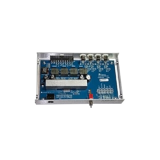
ICGOO电子元器件商城为您提供LM4673TMBD由Texas Instruments设计生产,在icgoo商城现货销售,并且可以通过原厂、代理商等渠道进行代购。 LM4673TMBD价格参考¥1178.54-¥1178.54。Texas InstrumentsLM4673TMBD封装/规格:评估板 - 音频放大器, LM4673 Boomer® 1-Channel (Mono) Output Class D Audio Amplifier Evaluation Board。您可以下载LM4673TMBD参考资料、Datasheet数据手册功能说明书,资料中有LM4673TMBD 详细功能的应用电路图电压和使用方法及教程。
| 参数 | 数值 |
| 产品目录 | 编程器,开发系统嵌入式解决方案 |
| 描述 | BOARD EVALUATION LM4673TM音频 IC 开发工具 LM4673TM EVAL BOARD |
| 产品分类 | |
| 品牌 | Texas Instruments |
| 产品手册 | http://www.ti.com/litv/SNAS317C |
| 产品图片 |
|
| rohs | 否含铅 / 不符合限制有害物质指令(RoHS)规范要求 |
| 产品系列 | 模拟与数字IC开发工具,音频 IC 开发工具,Texas Instruments LM4673TMBDBoomer® |
| 数据手册 | |
| 产品型号 | LM4673TMBD |
| 不同负载时的最大输出功率x通道数 | 2.65W x 1 @ 4 欧姆 |
| 产品 | Evaluation Boards |
| 产品种类 | 音频 IC 开发工具 |
| 使用的IC/零件 | LM4673 |
| 制造商产品页 | http://www.ti.com/general/docs/suppproductinfo.tsp?distId=10&orderablePartNumber=LM4673TMBD |
| 商标 | Texas Instruments |
| 工作温度 | -40°C ~ 85°C |
| 工作电源电压 | 5 V |
| 工具用于评估 | LM4673 |
| 工厂包装数量 | 1 |
| 所含物品 | 板 |
| 放大器类型 | D 类 |
| 板类型 | 完全填充 |
| 标准包装 | 1 |
| 电压-电源 | 2.4 V ~ 5.5 V |
| 相关产品 | /product-detail/zh/LM4673TMX%2FNOPB/LM4673TMX%2FNOPB-ND/1871627/product-detail/zh/LM4673TM%2FNOPB/LM4673TM%2FNOPBDKR-ND/1207568/product-detail/zh/LM4673TM%2FNOPB/LM4673TM%2FNOPBCT-ND/1207556/product-detail/zh/LM4673TM%2FNOPB/LM4673TM%2FNOPBTR-ND/1207544 |
| 类型 | Audio Amplifiers |
| 输出类型 | 1-通道(单声道) |


- 商务部:美国ITC正式对集成电路等产品启动337调查
- 曝三星4nm工艺存在良率问题 高通将骁龙8 Gen1或转产台积电
- 太阳诱电将投资9.5亿元在常州建新厂生产MLCC 预计2023年完工
- 英特尔发布欧洲新工厂建设计划 深化IDM 2.0 战略
- 台积电先进制程称霸业界 有大客户加持明年业绩稳了
- 达到5530亿美元!SIA预计今年全球半导体销售额将创下新高
- 英特尔拟将自动驾驶子公司Mobileye上市 估值或超500亿美元
- 三星加码芯片和SET,合并消费电子和移动部门,撤换高东真等 CEO
- 三星电子宣布重大人事变动 还合并消费电子和移动部门
- 海关总署:前11个月进口集成电路产品价值2.52万亿元 增长14.8%


PDF Datasheet 数据手册内容提取
LM4673, LM4673SDBD, LM4673TMBD www.ti.com SNAS317D–DECEMBER2005–REVISEDMAY2013 LM4673 Filterless, 2.65W, Mono, Class D Audio Power Amplifier CheckforSamples:LM4673,LM4673SDBD,LM4673TMBD FEATURES DESCRIPTION 1 • MonoClassDOperation The LM4673 is a single supply, high efficiency, 2 2.65W, mono, Class D audio amplifier. A low noise, • NoOutputFilterRequiredforInductiveLoads filterlessPWMarchitectureeliminatestheoutputfilter, • ExternallyConfigurableGain reducing external component count, board area • VeryFastTurnOnTime:17μs(typ) consumption,systemcost,andsimplifyingdesign. • MinimumExternalComponents The LM4673 is designed to meet the demands of • "ClickandPop"SuppressionCircuitry mobile phones and other portable communication devices. Operating on a single 5V supply, it is • Micro-PowerShutdownMode capable of driving a 4Ω speaker load at a continuous • AvailableinSpace-Saving0.4mmPitch average output of 2.1W with less than 1% THD+N. Its DSBGAandWSONPackages flexible power supply requirements allow operation from2.4Vto5.5V. APPLICATIONS The LM4673 has high efficiency with speaker loads • MobilePhones compared to a typical Class AB amplifier. With a 3.6V supply driving an 8Ω speaker, the IC's efficiency for a • PDAs 100mW power level is 80%, reaching 88% at 400mW • PortableElectronicDevices outputpower. KEY SPECIFICATIONS The LM4673 features a low-power consumption shutdown mode. Shutdown may be enabled by • Efficiencyat3.6V,400mWinto8Ω Speaker drivingtheShutdownpintoalogiclow(GND). 88%(typ) The gain of the LM4673 is externally configurable • Efficiencyat3.6V,100mWinto8Ω Speaker which allows independent gain control from multiple 80%(typ) sources by summing the signals. Output short circuit • Efficiencyat5V,1Winto8Ω Speaker86%(typ) and thermal overload protection prevent the device fromdamageduringfaultconditions. • QuiescentCurrent,3.6VSupply2.1mA(typ) • TotalShutdownPowerSupplyCurrent 0.01µA(typ) • SingleSupplyRange2.4Vto5.5V • PSRR,f=217Hz78dB 1 Pleasebeawarethatanimportantnoticeconcerningavailability,standardwarranty,anduseincriticalapplicationsof TexasInstrumentssemiconductorproductsanddisclaimerstheretoappearsattheendofthisdatasheet. Alltrademarksarethepropertyoftheirrespectiveowners. 2 PRODUCTIONDATAinformationiscurrentasofpublicationdate. Copyright©2005–2013,TexasInstrumentsIncorporated Products conform to specifications per the terms of the Texas Instruments standard warranty. Production processing does not necessarilyincludetestingofallparameters.
LM4673, LM4673SDBD, LM4673TMBD SNAS317D–DECEMBER2005–REVISEDMAY2013 www.ti.com Typical Application Figure1. TypicalAudioAmplifierApplicationCircuit Connection Diagram GND IN+ A Vo1 VDD B PGND IN- C Vo2 1 2 3 SHUTDOWN PVDD Figure2. 9-BumpDSBGA-TopView Figure3. 8-PinWSON-TopView SeeYFQ0009Package SeeNGQ0008A Thesedeviceshavelimitedbuilt-inESDprotection.Theleadsshouldbeshortedtogetherorthedeviceplacedinconductivefoam duringstorageorhandlingtopreventelectrostaticdamagetotheMOSgates. 2 SubmitDocumentationFeedback Copyright©2005–2013,TexasInstrumentsIncorporated ProductFolderLinks:LM4673 LM4673SDBD LM4673TMBD
LM4673, LM4673SDBD, LM4673TMBD www.ti.com SNAS317D–DECEMBER2005–REVISEDMAY2013 Absolute Maximum Ratings(1)(2)(3) SupplyVoltage(1) 6.0V StorageTemperature −65°Cto+150°C VoltageatAnyInputPin V +0.3V≥V≥GND-0.3V DD PowerDissipation(4) InternallyLimited ESDSusceptibility,allotherpins(5) 2.0kV ESDSusceptibility(6) 200V JunctionTemperature(T ) 150°C JMAX ThermalResistance θ (DSBGA) 99.1°C/W JA θ (WSON) 73°C/W JA SolderingInformation See(SNVA009)"microSMDWafersLevelChipScale Package." (1) Allvoltagesaremeasuredwithrespecttothegroundpin,unlessotherwisespecified. (2) AbsoluteMaximumRatingsindicatelimitsbeyondwhichdamagetothedevicemayoccur.OperatingRatingsindicateconditionsfor whichthedeviceisfunctional,butdonotguaranteespecificperformancelimits.ElectricalCharacteristicsstateDCandACelectrical specificationsunderparticulartestconditionswhichguaranteespecificperformancelimits.Thisassumesthatthedeviceiswithinthe OperatingRatings.Specificationsarenotguaranteedforparameterswherenolimitisgiven,however,thetypicalvalueisagood indicationofdeviceperformance. (3) IfMilitary/Aerospacespecifieddevicesarerequired,pleasecontacttheTISalesOffice/Distributorsforavailabilityandspecifications. (4) ThemaximumpowerdissipationmustbederatedatelevatedtemperaturesandisdictatedbyT ,θ ,andtheambienttemperature JMAX JA T .ThemaximumallowablepowerdissipationisP =(T –T )/θ orthenumbergiveninAbsoluteMaximumRatings,whichever A DMAX JMAX A JA islower.FortheLM4673,T =150°C.Thetypicalθ is99.1°C/WfortheDSBGApackage. JMAX JA (5) Humanbodymodel,100pFdischargedthrougha1.5kΩresistor. (6) MachineModel,220pF–240pFdischargedthroughallpins. Operating Ratings(1)(2) TemperatureRangeT ≤T ≤T −40°C≤T ≤85°C MIN A MAX A SupplyVoltage 2.4V≤V ≤5.5V DD (1) Allvoltagesaremeasuredwithrespecttothegroundpin,unlessotherwisespecified. (2) AbsoluteMaximumRatingsindicatelimitsbeyondwhichdamagetothedevicemayoccur.OperatingRatingsindicateconditionsfor whichthedeviceisfunctional,butdonotguaranteespecificperformancelimits.ElectricalCharacteristicsstateDCandACelectrical specificationsunderparticulartestconditionswhichguaranteespecificperformancelimits.Thisassumesthatthedeviceiswithinthe OperatingRatings.Specificationsarenotguaranteedforparameterswherenolimitisgiven,however,thetypicalvalueisagood indicationofdeviceperformance. Copyright©2005–2013,TexasInstrumentsIncorporated SubmitDocumentationFeedback 3 ProductFolderLinks:LM4673 LM4673SDBD LM4673TMBD
LM4673, LM4673SDBD, LM4673TMBD SNAS317D–DECEMBER2005–REVISEDMAY2013 www.ti.com Electrical Characteristics(1)(2) ThefollowingspecificationsapplyforA =2V/V(R =150kΩ),R =15µH+8Ω+15µHunlessotherwisespecified.Limits V I L applyforT =25°C. A LM4673 Units Symbol Parameter Conditions Typical(3) Limit(4)(5) (Limits) V =0V,A =2V/V, |V | DifferentialOutputOffsetVoltage I V 5 mV(max) OS V =2.4Vto5.0V DD |I | LogicHighInputCurrent V =5.0V,V =5.5V 17 100 μA(max) IH DD I |I | LogicLowInputCurrent V =5.0V,V =–0.3V 0.9 5 μA(max) IL DD I V =0V,NoLoad,V =5.0V 2.6 3.75 mA(max) IN DD V =0V,NoLoad,V =3.6V 2.1 2.9 mA IN DD V =0V,NoLoad,V =2.4V 1.7 2.3 mA(max) IN DD I QuiescentPowerSupplyCurrent DD V =0V,R =8Ω,V =5.0V 2.6 IN L DD V =0V,R =8Ω,V =3.6V 2.1 IN L DD V =0V,R =8Ω,V =2.4V 1.7 IN L DD I ShutdownCurrent(6) VSHUTDOWN=0V 0.01 1 μA(max) SD V =2.4Vto5.0V DD V Shutdownvoltageinputhigh 1.4 V(min) SDIH V Shutdownvoltageinputlow 0.4 V(max) SDIL R OutputImpedance V =0.4V 100 kΩ OSD SHUTDOWN 270kΩ/R V/V(min) A Gain 300kΩ/R I V I 330kΩ/R V/V(max) I ResistancefromShutdownPinto R 300 kΩ SD GND R =15μH+4Ω+15μH L THD=10%(max) f=1kHz,22kHzBW V =5V 2.65 W DD V =3.6V 1.3 W DD V =2.5V 550 mW DD P OutputPower O R =15μH+4Ω+15μH L THD=1%(max) f=1kHz,22kHzBW V =5V 2.15 W DD V =3.6V 1.06 W DD V =2.5V 450 mW DD (1) Allvoltagesaremeasuredwithrespecttothegroundpin,unlessotherwisespecified. (2) AbsoluteMaximumRatingsindicatelimitsbeyondwhichdamagetothedevicemayoccur.OperatingRatingsindicateconditionsfor whichthedeviceisfunctional,butdonotguaranteespecificperformancelimits.ElectricalCharacteristicsstateDCandACelectrical specificationsunderparticulartestconditionswhichguaranteespecificperformancelimits.Thisassumesthatthedeviceiswithinthe OperatingRatings.Specificationsarenotguaranteedforparameterswherenolimitisgiven,however,thetypicalvalueisagood indicationofdeviceperformance. (3) Typicalspecificationsarespecifiedat25°Candrepresenttheparametricnorm. (4) TestedlimitsareguaranteedtoTI'sAOQL(AverageOutgoingQualityLevel). (5) Datasheetmin/maxspecificationlimitsareguaranteedbydesign,test,orstatisticalanalysis. (6) Shutdowncurrentismeasuredinanormalroomenvironment.ExposuretodirectsunlightwillincreaseI byamaximumof2µA.The SD ShutdownpinshouldbedrivenascloseaspossibletoGNDforminimalshutdowncurrentandtoV forthebestTHDperformancein DD PLAYmode.SeetheApplicationInformationsectionunderSHUTDOWNFUNCTIONformoreinformation. 4 SubmitDocumentationFeedback Copyright©2005–2013,TexasInstrumentsIncorporated ProductFolderLinks:LM4673 LM4673SDBD LM4673TMBD
LM4673, LM4673SDBD, LM4673TMBD www.ti.com SNAS317D–DECEMBER2005–REVISEDMAY2013 Electrical Characteristics(1)(2) (continued) ThefollowingspecificationsapplyforA =2V/V(R =150kΩ),R =15µH+8Ω+15µHunlessotherwisespecified.Limits V I L applyforT =25°C. A LM4673 Units Symbol Parameter Conditions Typical(3) Limit(4)(5) (Limits) R =15μH+8Ω+15μH L THD=10%(max) f=1kHz,22kHzBW V =5V 1.7 W DD V =3.6V 870 mW DD V =2.5V 350 mW DD P OutputPower O R =15μH+8Ω+15μH L THD=1%(max) f=1kHz,22kHzBW V =5V 1.24 W DD V =3.6V 650 600 mW DD V =2.5V 300 mW DD V =5V,P =0.1W,f=1kHz 0.03 % DD O THD+N TotalHarmonicDistortion+Noise V =3.6V,P =0.1W,f=1kHz 0.02 % DD O V =2.5V,P =0.1W,f=1kHz 0.02 % DD O V =200mV Sine, Ripple PP f =217Hz,V =3.6,5V 78 dB Ripple DD PowerSupplyRejectionRatio InputstoACGND,CI=2μF PSRR (InputReferred) V =200mV Sine, Ripple PP f =1kHz,V =3.6,5V 72 dB Ripple DD InputstoACGND,C =2μF I SNR SignaltoNoiseRatio V =5V,P =1W 97 dB DD O RMS V =3.6V,f=20Hz–20kHz DD InputstoACGND,C =2μF 30 μV I RMS ε OutputNoise NoWeighting OUT (InputReferred) V =3.6V,InputstoACGND DD 23 μV C =2μF,AWeighted RMS I CommonModeRejectionRatio V =3.6V,V =1V Sine CMRR DD Ripple PP 70 dB (InputReferred) f =217Hz Ripple T Wake-upTime V =3.6V 17 μs WU DD T ShutdownTime 140 μs SD V =3.6V,P =400mW DD OUT 88 % R =8Ω L η Efficiency V =5V,P =1W DD OUT 86 % R =8Ω L External Components Description (Figure1) Components FunctionalDescription 1. C Supplybypasscapacitorwhichprovidespowersupplyfiltering.RefertothePowerSupplyBypassingsectionfor S informationconcerningproperplacementandselectionofthesupplybypasscapacitor. 2. C InputACcouplingcapacitorwhichblockstheDCvoltageattheamplifier'sinputterminals. I Copyright©2005–2013,TexasInstrumentsIncorporated SubmitDocumentationFeedback 5 ProductFolderLinks:LM4673 LM4673SDBD LM4673TMBD
LM4673, LM4673SDBD, LM4673TMBD SNAS317D–DECEMBER2005–REVISEDMAY2013 www.ti.com Typical Performance Characteristics TheperformancegraphsweretakenusingtheAudioPrecisionAUX-0025SwitchingAmplifiermeasurementFilterinseries withtheLCfilteronthedemoboard. THD+NvsOutputPower THD+NvsOutputPower f=1kHz,R =8Ω f=1kHz,R =4Ω L L 100 100 VDD = 5V VDD = 5V 10 10 VDD = 3.6V VDD = 3.6V +N (%) 1 VDD = 2.5V +N (%) 1 VDD = 2.5V D D H H T T 0.1 0.1 0.01 0.01 0.001 0.01 0.1 1 10 0.001 0.01 0.1 1 10 OUTPUT POWER (W) OUTPUT POWER (W) Figure4. Figure5. THD+NvsFrequency THD+NvsFrequency V =2.5V,P =100mW,R =8Ω V =3.6V,P =150mW,R =8Ω DD OUT L DD OUT L 100 100 10 10 %) 1 %) 1 N ( N ( + + D D H 0.1 H 0.1 T T 0.01 0.01 0.001 0.001 10 100 1000 10000 100000 10 100 1000 10000 100000 FREQUENCY (Hz) FREQUENCY (Hz) Figure6. Figure7. 6 SubmitDocumentationFeedback Copyright©2005–2013,TexasInstrumentsIncorporated ProductFolderLinks:LM4673 LM4673SDBD LM4673TMBD
LM4673, LM4673SDBD, LM4673TMBD www.ti.com SNAS317D–DECEMBER2005–REVISEDMAY2013 Typical Performance Characteristics (continued) TheperformancegraphsweretakenusingtheAudioPrecisionAUX-0025SwitchingAmplifiermeasurementFilterinseries withtheLCfilteronthedemoboard. THD+NvsFrequency THD+NvsFrequency V =5V,P =200mW,R =8Ω V =2.5V,P =100mW,R =4Ω DD OUT L DD OUT L 100 100 10 10 %) 1 %) 1 N ( N ( + + D D H 0.1 H 0.1 T T 0.01 0.01 0.001 0.001 10 100 1000 10000 100000 10 100 1000 10000 100000 FREQUENCY (Hz) FREQUENCY (Hz) Figure8. Figure9. THD+NvsFrequency THD+NvsFrequency V =3.6V,P =100mW,R =4Ω V =5V,P =150mW,R =4Ω DD OUT L DD OUT L 100 100 10 10 %) 1 %) 1 N ( N ( + + D D H 0.1 H 0.1 T T 0.01 0.01 0.001 0.001 10 100 1000 10000 100000 10 100 1000 10000 100000 FREQUENCY (Hz) FREQUENCY (Hz) Figure10. Figure11. Copyright©2005–2013,TexasInstrumentsIncorporated SubmitDocumentationFeedback 7 ProductFolderLinks:LM4673 LM4673SDBD LM4673TMBD
LM4673, LM4673SDBD, LM4673TMBD SNAS317D–DECEMBER2005–REVISEDMAY2013 www.ti.com Typical Performance Characteristics (continued) TheperformancegraphsweretakenusingtheAudioPrecisionAUX-0025SwitchingAmplifiermeasurementFilterinseries withtheLCfilteronthedemoboard. Efficiencyvs.OutputPower Efficiencyvs.OutputPower R =4Ω,f=1kHz R =8Ω,f=1kHz L L 100 100 90 90 VDD = 5V 80 80 VDD = 5V Y (%) 7600 VDD = 3.6V Y (%) 6700 VDVDD D= =2 .35.V6V ENC 50 VDD = 2.5V ENC 50 FICI 40 FICI 40 F F E 30 E 30 20 20 10 10 0 0 0 500 1000 1500 2000 2500 0 250 500 750 1000 1250 1500 OUTPUT POWER (mW) OUTPUT POWER (mW) Figure12. Figure13. PowerDissipationvs.OutputPower PowerDissipationvs.OutputPower R =4Ω,f=1kHz R =8Ω,f=1kHz L L 600 200 180 ON (%) 450000 VDD = 3.6V N (mW) 114600 VDD = 5V SSIPATI 300 VDD = 2.5V SIPATIO 110200 VDD = 3.6V WER DI 200 ER DIS 6800 O VDD = 5V W P O 40 100 P 20 VDD = 2.5V 0 0 0 200 400 600 800 1000 1200 0 250 500 750 1000 1250 1500 OUTPUT POWER (mW) OUTPUT POWER (mW) Figure14. Figure15. 8 SubmitDocumentationFeedback Copyright©2005–2013,TexasInstrumentsIncorporated ProductFolderLinks:LM4673 LM4673SDBD LM4673TMBD
LM4673, LM4673SDBD, LM4673TMBD www.ti.com SNAS317D–DECEMBER2005–REVISEDMAY2013 Typical Performance Characteristics (continued) TheperformancegraphsweretakenusingtheAudioPrecisionAUX-0025SwitchingAmplifiermeasurementFilterinseries withtheLCfilteronthedemoboard. OutputPowervs.SupplyVoltage OutputPowervs.SupplyVoltage R =4Ω,f=1kHz R =8Ω,f=1kHz L L 4000 2000 3500 1750 W) 3000 W) 1500 m m R ( 2500 R ( 1250 WE THD+N = 10% WE THD+N = 10% O 2000 O 1000 P P T T U 1500 U 750 P P T THD+N = 1% T THD+N = 1% U U O 1000 O 500 500 250 0 0 2.5 3 3.5 4 4.5 5 5.5 2.5 3 3.5 4 4.5 5 5.5 SUPPLY VOLTAGE (V) SUPPLY VOLTAGE (V) Figure16. Figure17. PSRRvs.Frequency CMRRvs.Frequency V =3.6V,V =200mV ,R =8Ω V =3.6V,V =1V ,R =8Ω DD RIPPLE P-P L DD CM P-P L 0 0 -10 -10 -20 -20 -30 -30 B) B) d -40 d -40 R ( R( SR -50 MR -50 P C -60 -60 -70 -70 -80 -80 -90 -90 10 100 1000 10000 100000 10 100 1000 10000 100000 FREQUENCY (Hz) FREQUENCY (Hz) Figure18. Figure19. Copyright©2005–2013,TexasInstrumentsIncorporated SubmitDocumentationFeedback 9 ProductFolderLinks:LM4673 LM4673SDBD LM4673TMBD
LM4673, LM4673SDBD, LM4673TMBD SNAS317D–DECEMBER2005–REVISEDMAY2013 www.ti.com Typical Performance Characteristics (continued) TheperformancegraphsweretakenusingtheAudioPrecisionAUX-0025SwitchingAmplifiermeasurementFilterinseries withtheLCfilteronthedemoboard. SupplyCurrentvs.SupplyVoltage NoLoad 4 3.5 A) 3 m T ( N 2.5 E R R 2 U C Y 1.5 L P P U 1 S 0.5 0 2.5 3 3.5 4 4.5 5 5.5 SUPPLY VOLTAGE (V) Figure20. 10 SubmitDocumentationFeedback Copyright©2005–2013,TexasInstrumentsIncorporated ProductFolderLinks:LM4673 LM4673SDBD LM4673TMBD
LM4673, LM4673SDBD, LM4673TMBD www.ti.com SNAS317D–DECEMBER2005–REVISEDMAY2013 APPLICATION INFORMATION GENERAL AMPLIFIER FUNCTION TheLM4673featuresafilterlessmodulationscheme.Thedifferentialoutputsofthedeviceswitchat300kHzfrom V to GND. When there is no input signal applied, the two outputs (V 1 and V 2) switch with a 50% duty cycle, DD O O with both outputs in phase. Because the outputs of the LM4673 are differential, the two signals cancel each other. This results in no net voltage across the speaker, thus there is no load current during an idle state, conservingpower. With an input signal applied, the duty cycle (pulse width) of the LM4673 outputs changes. For increasing output voltages,thedutycycleofV 1increases,whilethedutycycleofV 2decreases.Fordecreasingoutputvoltages, O O the converse occurs, the duty cycle of V 2 increases while the duty cycle of V 1 decreases. The difference O O betweenthetwopulsewidthsyieldsthedifferentialoutputvoltage. POWER DISSIPATION AND EFFICIENCY Ingeneralterms,efficiencyisconsideredtobetheratioofusefulworkoutputdividedbythetotalenergyrequired toproduceitwiththedifferencebeingthepowerdissipated,typically,intheIC.Thekeyhereis“useful” work.For audio systems, the energy delivered in the audible bands is considered useful including the distortion products of the input signal. Sub-sonic (DC) and super-sonic components (>22kHz) are not useful. The difference between the power flowing from the power supply and the audio band power being transduced is dissipated in the LM4673 and in the transducer load. The amount of power dissipation in the LM4673 is very low. This is because the ON resistance of the switches used to form the output waveforms is typically less than 0.25Ω. This leaves only the transducer load as a potential "sink" for the small excess of input power over audio band output power. The LM4673 dissipates only a fraction of the excess power requiring no additional PCB area or copper plane to actasaheatsink. DIFFERENTIAL AMPLIFIER EXPLANATION As logic supply voltages continue to shrink, designers are increasingly turning to differential analog signal handling to preserve signal to noise ratios with restricted voltage swing. The LM4673 is a fully differential amplifierthatfeaturesdifferentialinputandoutputstages.Adifferentialamplifieramplifiesthedifferencebetween the two input signals. Traditional audio power amplifiers have typically offered only single-ended inputs resulting in a 6dB reduction in signal to noise ratio relative to differential inputs. The LM4673 also offers the possibility of DC input coupling which eliminates the two external AC coupling, DC blocking capacitors. The LM4673 can be used, however, as a single ended input amplifier while still retaining it's fully differential benefits. In fact, completely unrelated signals may be placed on the input pins. The LM4673 simply amplifies the difference between the signals. A major benefit of a differential amplifier is the improved common mode rejection ratio (CMRR) over single input amplifiers. The common-mode rejection characteristic of the differential amplifier reducessensitivitytogroundoffsetrelatednoiseinjection,especiallyimportantinhighnoiseapplications. PCB LAYOUT CONSIDERATIONS As output power increases, interconnect resistance (PCB traces and wires) between the amplifier, load and power supply create a voltage drop. The voltage loss on the traces between the LM4673 and the load results is lower output power and decreased efficiency. Higher trace resistance between the supply and the LM4673 has the same effect as a poorly regulated supply, increased ripple on the supply line also reducing the peak output power. The effects of residual trace resistance increases as output current increases due to higher output power, decreased load impedance or both. To maintain the highest output voltage swing and corresponding peak output power, the PCB traces that connect the output pins to the load and the supply pins to the power supply should beaswideaspossibletominimizetraceresistance. TheuseofpowerandgroundplaneswillgivethebestTHD+Nperformance.Whilereducingtraceresistance,the useofpowerplanesalsocreatesparasitecapacitorsthathelptofilterthepowersupplyline. Copyright©2005–2013,TexasInstrumentsIncorporated SubmitDocumentationFeedback 11 ProductFolderLinks:LM4673 LM4673SDBD LM4673TMBD
LM4673, LM4673SDBD, LM4673TMBD SNAS317D–DECEMBER2005–REVISEDMAY2013 www.ti.com The inductive nature of the transducer load can also result in overshoot on one or both edges, clamped by the parasitic diodes to GND and V in each case. From an EMI standpoint, this is an aggressive waveform that can DD radiate or conduct to other components in the system and cause interference. It is essential to keep the power and output traces short and well shielded if possible. Use of ground planes, beads, and micro-strip layout techniquesareallusefulinpreventingunwantedinterference. As the distance from the LM4673 and the speaker increase, the amount of EMI radiation will increase since the output wires or traces acting as antenna become more efficient with length. What is acceptable EMI is highly application specific. Ferrite chip inductors placed close to the LM4673 may be needed to reduce EMI radiation. Thevalueoftheferritechipisveryapplicationspecific. POWER SUPPLY BYPASSING As with any power amplifier, proper supply bypassing is critical for low noise performance and high power supply rejection ratio (PSRR). The capacitor (C ) location should be as close as possible to the LM4673. Typical S applications employ a voltage regulator with a 10µF and a 0.1µF bypass capacitors that increase supply stability. These capacitors do not eliminate the need for bypassing on the supply pin of the LM4673. A 4.7µF tantalum capacitorisrecommended. SHUTDOWN FUNCTION In order to reduce power consumption while not in use, the LM4673 contains shutdown circuitry that reduces current draw to less than 0.01µA. The trigger point for shutdown is shown as a typical value in the Electrical Characteristics Tables and in the Shutdown Hysteresis Voltage graphs found in the Typical Performance Characteristics section. It is best to switch between ground and supply for minimum current usage while in the shutdown state. While the LM4673 may be disabled with shutdown voltages in between ground and supply, the idlecurrentwillbegreaterthanthetypical0.01µAvalue. TheLM4673hasaninternalresistorconnectedbetweenGNDandShutdownpins.Thepurposeofthisresistoris toeliminateanyunwantedstatechangeswhentheShutdownpinisfloating.TheLM4673willentertheshutdown state when the Shutdown pin is left floating or if not floating, when the shutdown voltage has crossed the threshold. To minimize the supply current while in the shutdown state, the Shutdown pin should be driven to GNDorleftfloating.IftheShutdownpinisnotdriventoGND,theamountofadditionalresistorcurrentduetothe internalshutdownresistorcanbefoundbyEquation1below. (V -GND)/300kΩ (1) SD Withonlya0.5Vdifference,anadditional1.7µAofcurrentwillbedrawnwhileintheshutdownstate. PROPER SELECTION OF EXTERNAL COMPONENTS The gain of the LM4673 is set by the external resistors, Ri in Typical Application, The Gain is given by Equation2below.BestTHD+Nperformanceisachievedwithagainof2V/V(6dB). A =2*150kΩ/R (V/V) (2) V i It is recommended that resistors with 1% tolerance or better be used to set the gain of the LM4673. The Ri resistors should be placed close to the input pins of the LM4673. Keeping the input traces close to each other and of the same length in a high noise environment will aid in noise rejection due to the good CMRR of the LM4673. Noise coupled onto input traces which are physically close to each other will be common mode and easilyrejectedbytheLM4673. Input capacitors may be needed for some applications or when the source is single-ended (see Figure 22, Figure 24). Input capacitors are needed to block any DC voltage at the source so that the DC voltage seen between the input terminals of the LM4673 is 0V. Input capacitors create a high-pass filter with the input resistors,R.The–3dBpointofthehigh-passfilterisfoundusingEquation3below. i f =1/(2πR C )(Hz) (3) C i i The input capacitors may also be used to remove low audio frequencies. Small speakers cannot reproduce low bass frequencies so filtering may be desired . When the LM4673 is using a single-ended source, power supply noise on the ground is seen as an input signal by the +IN input pin that is capacitor coupled to ground (See Figure 24 – Figure 26). Setting the high-pass filter point above the power supply noise frequencies, 217Hz in a GSM phone, for example, will filter out this noise so it is not amplified and heard on the output. Capacitors with a toleranceof10%orbetterarerecommendedforimpedancematching. 12 SubmitDocumentationFeedback Copyright©2005–2013,TexasInstrumentsIncorporated ProductFolderLinks:LM4673 LM4673SDBD LM4673TMBD
LM4673, LM4673SDBD, LM4673TMBD www.ti.com SNAS317D–DECEMBER2005–REVISEDMAY2013 DIFFERENTIAL CIRCUIT CONFIGURATIONS The LM4673 can be used in many different circuit configurations. The simplest and best performing is the DC coupled, differential input configuration shown in Figure 21. Equation 2 above is used to determine the value of theR resistorsforadesiredgain. i Input capacitors can be used in a differential configuration as shown in Figure 22. Equation 3 above is used to determine the value of the C capacitors for a desired frequency response due to the high-pass filter created by i C andR.Equation2aboveisusedtodeterminethevalueoftheR resistorsforadesiredgain. i i i The LM4673 can be used to amplify more than one audio source. Figure 23 shows a dual differential input configuration. The gain for each input can be independently set for maximum design flexibility using the R i resistors for each input and Equation 2. Input capacitors can be used with one or more sources as well to have differentfrequencyresponsesdependingonthesourceorifaDCvoltageneedstobeblockedfromasource. SINGLE-ENDED CIRCUIT CONFIGURATIONS The LM4673 can also be used with single-ended sources but input capacitors will be needed to block any DC at the input terminals. Figure 24 shows the typical single-ended application configuration. The equations for Gain, Equation2,andfrequencyresponse,Equation3,holdforthesingle-endedconfigurationasshowninFigure24. When using more than one single-ended source as shown in Figure 25, the impedance seen from each input terminal should be equal. To find the correct values for C and R connected to the +IN input pin the equivalent i3 i3 impedanceofallthesingle-endedsourcesarecalculated.Thesingle-endedsourcesareinparalleltoeachother. The equivalent capacitor and resistor, C and R , are found by calculating the parallel combination of all i3 i3 CvaluesandthenallR values.Equation4andEquation5belowareforanynumberofsingle-endedsources. i i C =C +C +C ...(F) (4) i3 i1 i2 in R =1/(1/R +1/R +1/R ...)(Ω) (5) i3 i1 i2 in The LM4673 may also use a combination of single-ended and differential sources. A typical application with one single-ended source and one differential source is shown in Figure 26. Using the principle of superposition, the externalcomponentvaluescanbedeterminedwiththeaboveequationscorrespondingtotheconfiguration. Figure21. DifferentialInputConfiguration Copyright©2005–2013,TexasInstrumentsIncorporated SubmitDocumentationFeedback 13 ProductFolderLinks:LM4673 LM4673SDBD LM4673TMBD
LM4673, LM4673SDBD, LM4673TMBD SNAS317D–DECEMBER2005–REVISEDMAY2013 www.ti.com Figure22. DifferentialInputConfigurationwithInputCapacitors Figure23. DualDifferentialInputConfiguration Figure24. Single-EndedInputConfiguration 14 SubmitDocumentationFeedback Copyright©2005–2013,TexasInstrumentsIncorporated ProductFolderLinks:LM4673 LM4673SDBD LM4673TMBD
LM4673, LM4673SDBD, LM4673TMBD www.ti.com SNAS317D–DECEMBER2005–REVISEDMAY2013 Figure25. DualSingle-EndedInputConfiguration Figure26. DualInputwithaSingle-EndedInputandaDifferentialInput Copyright©2005–2013,TexasInstrumentsIncorporated SubmitDocumentationFeedback 15 ProductFolderLinks:LM4673 LM4673SDBD LM4673TMBD
LM4673, LM4673SDBD, LM4673TMBD SNAS317D–DECEMBER2005–REVISEDMAY2013 www.ti.com REFERENCE DESIGN BOARD SCHEMATIC In addition to the minimal parts required for the application circuit, a measurement filter is provided on the evaluation circuit board so that conventional audio measurements can be conveniently made without additional equipment. This is a balanced input, grounded differential output low pass filter with a 3dB frequency of approximately35kHzandanonboardterminationresistorof300Ω (seeschematic).Notethatthecapacitiveload elements are returned to ground. This is not optimal for common mode rejection purposes, but due to the independent pulse format at each output there is a significant amount of high frequency common mode component on the outputs. The grounded capacitive filter elements attenuate this component at the board to reducethehighfrequencyCMRRrequirementplacedontheanalysisinstruments. Even with the grounded filter the audio signal is still differential, necessitating a differential input on any analysis instrument connected to it. Most lab instruments that feature BNC connectors on their inputs are NOT differential respondingbecausetheringoftheBNCisusuallygrounded. The commonly used Audio Precision analyzer is differential, but its ability to accurately reject high frequency signals is questionable necessitating the on board measurement filter. When in doubt or when the signal needs to be single-ended, use an audio signal transformer to convert the differential output to a single ended output. Depending on the audio transformer's characteristics, there may be some attenuation of the audio signal which needstobetakenintoaccountforcorrectmeasurementofperformance. Measurements made at the output of the measurement filter suffer attenuation relative to the primary, unfiltered outputs even at audio frequencies. This is due to the resistance of the inductors interacting with the termination resistor (300Ω) and is typically about -0.25dB (3%). In other words, the voltage levels (and corresponding power levels) indicated through the measurement filter are slightly lower than those that actually occur at the load placed on the unfiltered outputs. This small loss in the filter for measurement gives a lower output power reading thanwhatisreallyoccurringontheunfilteredoutputsanditsload. 16 SubmitDocumentationFeedback Copyright©2005–2013,TexasInstrumentsIncorporated ProductFolderLinks:LM4673 LM4673SDBD LM4673TMBD
LM4673, LM4673SDBD, LM4673TMBD www.ti.com SNAS317D–DECEMBER2005–REVISEDMAY2013 LM4673SD Demo Board Artwork TopSilkscreen TopLayer CompositeView InternalLayer1 InternalLayer2 BottomSilkscreen Copyright©2005–2013,TexasInstrumentsIncorporated SubmitDocumentationFeedback 17 ProductFolderLinks:LM4673 LM4673SDBD LM4673TMBD
LM4673, LM4673SDBD, LM4673TMBD SNAS317D–DECEMBER2005–REVISEDMAY2013 www.ti.com BottomLayer LM4673TM Demo Board Artwork TopSilkscreen TopLayer 18 SubmitDocumentationFeedback Copyright©2005–2013,TexasInstrumentsIncorporated ProductFolderLinks:LM4673 LM4673SDBD LM4673TMBD
LM4673, LM4673SDBD, LM4673TMBD www.ti.com SNAS317D–DECEMBER2005–REVISEDMAY2013 CompositeView InternalLayer1 InternalLayer2 BottomSilkscreen Copyright©2005–2013,TexasInstrumentsIncorporated SubmitDocumentationFeedback 19 ProductFolderLinks:LM4673 LM4673SDBD LM4673TMBD
LM4673, LM4673SDBD, LM4673TMBD SNAS317D–DECEMBER2005–REVISEDMAY2013 www.ti.com BottomLayer 20 SubmitDocumentationFeedback Copyright©2005–2013,TexasInstrumentsIncorporated ProductFolderLinks:LM4673 LM4673SDBD LM4673TMBD
LM4673, LM4673SDBD, LM4673TMBD www.ti.com SNAS317D–DECEMBER2005–REVISEDMAY2013 REVISION HISTORY Rev Date Description 1.0 12/16/05 InitialWEBreleased. 1.1 02/28/06 Takenout“FutureProduct”,thenre-WEBdthe datasheet. 1.2 04/06/06 AddedtheTMandSDdemoboards,then releasedtotheWEB(perRoyce). 1.3 11/01/07 DeletedasentenceundertheSHUTDOWN FUNCTIONsection. ChangesfromRevisionC(May2013)toRevisionD Page • ChangedlayoutofNationalDataSheettoTIformat.......................................................................................................... 19 Copyright©2005–2013,TexasInstrumentsIncorporated SubmitDocumentationFeedback 21 ProductFolderLinks:LM4673 LM4673SDBD LM4673TMBD
PACKAGE OPTION ADDENDUM www.ti.com 6-Feb-2020 PACKAGING INFORMATION Orderable Device Status Package Type Package Pins Package Eco Plan Lead/Ball Finish MSL Peak Temp Op Temp (°C) Device Marking Samples (1) Drawing Qty (2) (6) (3) (4/5) LM4673SD/NOPB ACTIVE WSON NGQ 8 1000 Green (RoHS SN Level-1-260C-UNLIM -40 to 85 L4673 & no Sb/Br) LM4673TM/NOPB ACTIVE DSBGA YFQ 9 250 Green (RoHS SNAGCU Level-1-260C-UNLIM -40 to 85 G & no Sb/Br) G4 LM4673TMX/NOPB ACTIVE DSBGA YFQ 9 3000 Green (RoHS SNAGCU Level-1-260C-UNLIM -40 to 85 G & no Sb/Br) G4 (1) The marketing status values are defined as follows: ACTIVE: Product device recommended for new designs. LIFEBUY: TI has announced that the device will be discontinued, and a lifetime-buy period is in effect. NRND: Not recommended for new designs. Device is in production to support existing customers, but TI does not recommend using this part in a new design. PREVIEW: Device has been announced but is not in production. Samples may or may not be available. OBSOLETE: TI has discontinued the production of the device. (2) RoHS: TI defines "RoHS" to mean semiconductor products that are compliant with the current EU RoHS requirements for all 10 RoHS substances, including the requirement that RoHS substance do not exceed 0.1% by weight in homogeneous materials. Where designed to be soldered at high temperatures, "RoHS" products are suitable for use in specified lead-free processes. TI may reference these types of products as "Pb-Free". RoHS Exempt: TI defines "RoHS Exempt" to mean products that contain lead but are compliant with EU RoHS pursuant to a specific EU RoHS exemption. Green: TI defines "Green" to mean the content of Chlorine (Cl) and Bromine (Br) based flame retardants meet JS709B low halogen requirements of <=1000ppm threshold. Antimony trioxide based flame retardants must also meet the <=1000ppm threshold requirement. (3) MSL, Peak Temp. - The Moisture Sensitivity Level rating according to the JEDEC industry standard classifications, and peak solder temperature. (4) There may be additional marking, which relates to the logo, the lot trace code information, or the environmental category on the device. (5) Multiple Device Markings will be inside parentheses. Only one Device Marking contained in parentheses and separated by a "~" will appear on a device. If a line is indented then it is a continuation of the previous line and the two combined represent the entire Device Marking for that device. (6) Lead/Ball Finish - Orderable Devices may have multiple material finish options. Finish options are separated by a vertical ruled line. Lead/Ball Finish values may wrap to two lines if the finish value exceeds the maximum column width. Important Information and Disclaimer:The information provided on this page represents TI's knowledge and belief as of the date that it is provided. TI bases its knowledge and belief on information provided by third parties, and makes no representation or warranty as to the accuracy of such information. Efforts are underway to better integrate information from third parties. TI has taken and continues to take reasonable steps to provide representative and accurate information but may not have conducted destructive testing or chemical analysis on incoming materials and chemicals. TI and TI suppliers consider certain information to be proprietary, and thus CAS numbers and other limited information may not be available for release. Addendum-Page 1
PACKAGE OPTION ADDENDUM www.ti.com 6-Feb-2020 In no event shall TI's liability arising out of such information exceed the total purchase price of the TI part(s) at issue in this document sold by TI to Customer on an annual basis. Addendum-Page 2
PACKAGE MATERIALS INFORMATION www.ti.com 12-Aug-2013 TAPE AND REEL INFORMATION *Alldimensionsarenominal Device Package Package Pins SPQ Reel Reel A0 B0 K0 P1 W Pin1 Type Drawing Diameter Width (mm) (mm) (mm) (mm) (mm) Quadrant (mm) W1(mm) LM4673SD/NOPB WSON NGQ 8 1000 178.0 12.4 3.3 3.3 1.0 8.0 12.0 Q1 LM4673TM/NOPB DSBGA YFQ 9 250 178.0 8.4 1.5 1.5 0.76 4.0 8.0 Q1 LM4673TMX/NOPB DSBGA YFQ 9 3000 178.0 8.4 1.5 1.5 0.76 4.0 8.0 Q1 PackMaterials-Page1
PACKAGE MATERIALS INFORMATION www.ti.com 12-Aug-2013 *Alldimensionsarenominal Device PackageType PackageDrawing Pins SPQ Length(mm) Width(mm) Height(mm) LM4673SD/NOPB WSON NGQ 8 1000 210.0 185.0 35.0 LM4673TM/NOPB DSBGA YFQ 9 250 210.0 185.0 35.0 LM4673TMX/NOPB DSBGA YFQ 9 3000 210.0 185.0 35.0 PackMaterials-Page2
MECHANICALDATA YFQ0009xxx D 0.600±0.075 E TMD09XXX(RevA) D: Max = 1.397 mm, Min =1 .336 mm E: Max = 1.397 mm, Min =1 .336 mm 4215077/A 12/12 NOTES: A.Alllineardimensionsareinmillimeters.DimensioningandtolerancingperASMEY14.5M-1994. B.Thisdrawingissubjecttochangewithoutnotice. www.ti.com
PACKAGE OUTLINE NGQ0008A WSON - 0.8 mm max height SCALE 4.000 PLASTIC SMALL OUTLINE - NO LEAD 3.1 A B 2.9 PIN 1 INDEX AREA 3.1 2.9 0.8 C 0.7 SEATING PLANE 0.08 C 1.6 0.1 (0.1) TYP SYMM 0.05 EXPOSED 0.00 THERMAL PAD 4 5 9 SYMM 2X 2 0.1 1.5 8 1 6X 0.5 0.3 8X 0.2 PIN 1 ID 8X 0.5 0.1 C A B 0.3 0.05 C 4214922/A 03/2018 NOTES: 1. All linear dimensions are in millimeters. Any dimensions in parenthesis are for reference only. Dimensioning and tolerancing per ASME Y14.5M. 2. This drawing is subject to change without notice. 3. The package thermal pad must be soldered to the printed circuit board for thermal and mechanical performance. www.ti.com
EXAMPLE BOARD LAYOUT NGQ0008A WSON - 0.8 mm max height PLASTIC SMALL OUTLINE - NO LEAD (1.6) 8X (0.6) SYMM 1 8 (0.75) 8X (0.25) 9 SYMM (2) 6X (0.5) 5 4 (R0.05) TYP ( 0.2) VIA TYP (2.8) LAND PATTERN EXAMPLE EXPOSED METAL SHOWN SCALE:20X 0.07 MAX 0.07 MIN ALL AROUND ALL AROUND EXPOSED METAL EXPOSED METAL SOLDER MASK METAL METAL UNDER SOLDER MASK OPENING SOLDER MASK OPENING NON SOLDER MASK SOLDER MASK DEFINED DEFINED (PREFERRED) SOLDER MASK DETAILS 4214922/A 03/2018 NOTES: (continued) 4. This package is designed to be soldered to a thermal pad on the board. For more information, see Texas Instruments literature number SLUA271 (www.ti.com/lit/slua271). 5. Vias are optional depending on application, refer to device data sheet. If any vias are implemented, refer to their locations shown on this view. It is recommended that vias under paste be filled, plugged or tented. www.ti.com
EXAMPLE STENCIL DESIGN NGQ0008A WSON - 0.8 mm max height PLASTIC SMALL OUTLINE - NO LEAD 8X (0.6) SYMM METAL TYP 9 1 8 8X (0.25) SYMM (1.79) 6X (0.5) 5 4 (R0.05) TYP (1.47) (2.8) SOLDER PASTE EXAMPLE BASED ON 0.1 mm THICK STENCIL EXPOSED PAD 9: 82% PRINTED SOLDER COVERAGE BY AREA UNDER PACKAGE SCALE:20X 4214922/A 03/2018 NOTES: (continued) 6. Laser cutting apertures with trapezoidal walls and rounded corners may offer better paste release. IPC-7525 may have alternate design recommendations. www.ti.com
IMPORTANTNOTICEANDDISCLAIMER TI PROVIDES TECHNICAL AND RELIABILITY DATA (INCLUDING DATASHEETS), DESIGN RESOURCES (INCLUDING REFERENCE DESIGNS), APPLICATION OR OTHER DESIGN ADVICE, WEB TOOLS, SAFETY INFORMATION, AND OTHER RESOURCES “AS IS” AND WITH ALL FAULTS, AND DISCLAIMS ALL WARRANTIES, EXPRESS AND IMPLIED, INCLUDING WITHOUT LIMITATION ANY IMPLIED WARRANTIES OF MERCHANTABILITY, FITNESS FOR A PARTICULAR PURPOSE OR NON-INFRINGEMENT OF THIRD PARTY INTELLECTUAL PROPERTY RIGHTS. These resources are intended for skilled developers designing with TI products. You are solely responsible for (1) selecting the appropriate TI products for your application, (2) designing, validating and testing your application, and (3) ensuring your application meets applicable standards, and any other safety, security, or other requirements. These resources are subject to change without notice. TI grants you permission to use these resources only for development of an application that uses the TI products described in the resource. Other reproduction and display of these resources is prohibited. No license is granted to any other TI intellectual property right or to any third party intellectual property right. TI disclaims responsibility for, and you will fully indemnify TI and its representatives against, any claims, damages, costs, losses, and liabilities arising out of your use of these resources. TI’s products are provided subject to TI’s Terms of Sale (www.ti.com/legal/termsofsale.html) or other applicable terms available either on ti.com or provided in conjunction with such TI products. TI’s provision of these resources does not expand or otherwise alter TI’s applicable warranties or warranty disclaimers for TI products. Mailing Address: Texas Instruments, Post Office Box 655303, Dallas, Texas 75265 Copyright © 2020, Texas Instruments Incorporated