ICGOO在线商城 > LM3S6965-IBZ50-A2

 Datasheet下载
- 型号: LM3S6965-IBZ50-A2
- 制造商: Texas Instruments
- 库位|库存: xxxx|xxxx
- 要求:
| 数量阶梯 | 香港交货 | 国内含税 |
| +xxxx | $xxxx | ¥xxxx |
查看当月历史价格
查看今年历史价格
LM3S6965-IBZ50-A2产品简介:
ICGOO电子元器件商城为您提供LM3S6965-IBZ50-A2由Texas Instruments设计生产,在icgoo商城现货销售,并且可以通过原厂、代理商等渠道进行代购。 提供LM3S6965-IBZ50-A2价格参考以及Texas InstrumentsLM3S6965-IBZ50-A2封装/规格参数等产品信息。 你可以下载LM3S6965-IBZ50-A2参考资料、Datasheet数据手册功能说明书, 资料中有LM3S6965-IBZ50-A2详细功能的应用电路图电压和使用方法及教程。
| 参数 | 数值 |
| 产品目录 | 集成电路 (IC) |
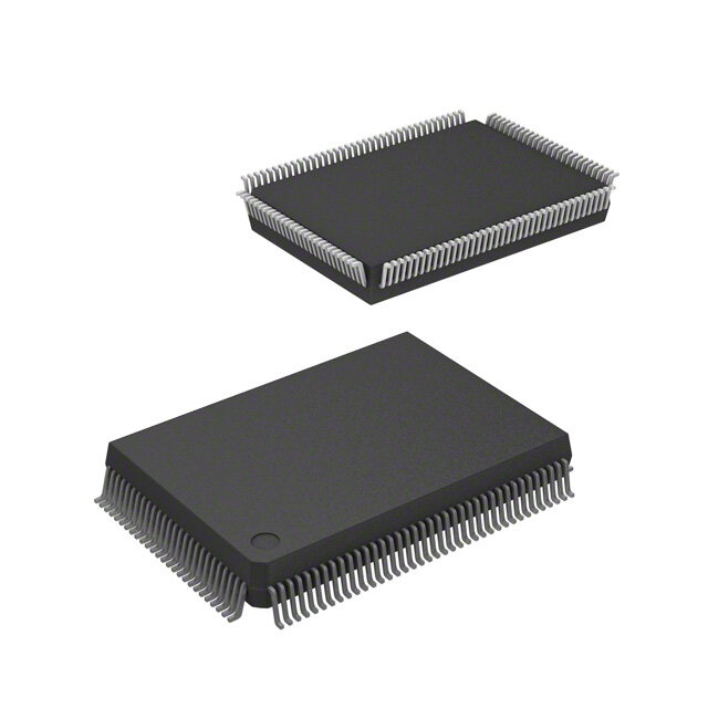
| 描述 | IC MCU 32BIT 256KB FLASH 108BGA |
| EEPROM容量 | - |
| 产品分类 | |
| I/O数 | 42 |
| 品牌 | Texas Instruments |
| 数据手册 | http://www.ti.com/lit/pdf/spms144ghttp://www.ti.com/lit/pdf/spmu055点击此处下载产品Datasheethttp://www.ti.com/lit/pdf/spmu023http://www.ti.com/lit/pdf/spmu058http://www.ti.com/lit/pdf/spmu029http://www.ti.com/lit/pdf/spmu007 |
| 产品图片 |
|
| 产品型号 | LM3S6965-IBZ50-A2 |
| RAM容量 | 64K x 8 |
| rohs | 无铅 / 符合限制有害物质指令(RoHS)规范要求 |
| 产品系列 | Stellaris® ARM® Cortex™-M3S 6000 |
| 产品培训模块 | http://www.digikey.cn/PTM/IndividualPTM.page?site=cn&lang=zhs&ptm=30354 |
| 供应商器件封装 | 108-BGA (10x10) |
| 其它名称 | 726-1166 |
| 制造商产品页 | http://www.ti.com/general/docs/suppproductinfo.tsp?distId=10&orderablePartNumber=LM3S6965-IBZ50-A2 |
| 包装 | 托盘 |
| 外设 | 欠压检测/复位,POR,PWM,WDT |
| 封装/外壳 | 108-LFBGA |
| 工作温度 | -40°C ~ 85°C |
| 振荡器类型 | 内部 |
| 数据转换器 | A/D 4x10b |
| 标准包装 | 184 |
| 核心处理器 | ARM® Cortex™-M3 |
| 核心尺寸 | 32-位 |
| 电压-电源(Vcc/Vdd) | 2.25 V ~ 2.75 V |
| 程序存储器类型 | 闪存 |
| 程序存储容量 | 256KB(256K x 8) |
| 连接性 | 以太网, I²C, IrDA, Microwire, QEI, SPI, SSI, UART/USART |
| 速度 | 50MHz |
| 配用 | /product-detail/zh/EKT-LM3S6965/726-1132-ND/1794062/product-detail/zh/EKK-LM3S6965/726-1054-ND/1626527/product-detail/zh/EKI-LM3S6965/726-1052-ND/1626525/product-detail/zh/EKC-LM3S6965/726-1050-ND/1626523 |


PDF Datasheet 数据手册内容提取
TEXAS INSTRUMENTS-PRODUCTION DATA ® Stellaris LM3S6965 Microcontroller DATA SHEET DS-LM3S6965-15852.2743 Copyright © 2007-2014 SPMS144I Texas Instruments Incorporated
Copyright Copyright©2007-2014TexasInstrumentsIncorporatedAllrightsreserved.StellarisandStellarisWare®areregisteredtrademarksofTexasInstruments Incorporated.ARMandThumbareregisteredtrademarksandCortexisatrademarkofARMLimited.Othernamesandbrandsmaybeclaimedasthe propertyofothers. PRODUCTIONDATAinformationiscurrentasofpublicationdate.ProductsconformtospecificationsperthetermsofTexasInstrumentsstandard warranty.Productionprocessingdoesnotnecessarilyincludetestingofallparameters. Pleasebeawarethatanimportantnoticeconcerningavailability,standardwarranty,anduseincriticalapplicationsofTexasInstrumentssemiconductor productsanddisclaimerstheretoappearsattheendofthisdatasheet. TexasInstrumentsIncorporated 108WildBasin,Suite350 Austin,TX78746 http://www.ti.com/stellaris http://www-k.ext.ti.com/sc/technical-support/product-information-centers.htm 2 July15,2014 TexasInstruments-ProductionData
Stellaris®LM3S6965Microcontroller Table of Contents Revision History .............................................................................................................................25 About This Document ....................................................................................................................32 Audience .............................................................................................................................................. 32 About This Manual ................................................................................................................................ 32 RelatedDocuments............................................................................................................................... 32 Documentation Conventions .................................................................................................................. 33 1 Architectural Overview ..........................................................................................35 1.1 Product Features .......................................................................................................... 35 1.2 Target Applications ........................................................................................................ 44 1.3 High-Level Block Diagram ............................................................................................. 44 1.4 Functional Overview ...................................................................................................... 46 1.4.1 ARMCortex™-M3......................................................................................................... 46 1.4.2 Motor Control Peripherals .............................................................................................. 47 1.4.3 Analog Peripherals ........................................................................................................ 48 1.4.4 Serial Communications Peripherals ................................................................................ 48 1.4.5 System Peripherals ....................................................................................................... 50 1.4.6 Memory Peripherals ...................................................................................................... 51 1.4.7 Additional Features ....................................................................................................... 51 1.4.8 Hardware Details .......................................................................................................... 52 2 The Cortex-M3 Processor ......................................................................................53 2.1 Block Diagram .............................................................................................................. 54 2.2 Overview ...................................................................................................................... 55 2.2.1 System-Level Interface .................................................................................................. 55 2.2.2 Integrated Configurable Debug ...................................................................................... 55 2.2.3 Trace Port Interface Unit (TPIU) ..................................................................................... 56 2.2.4 Cortex-M3 System Component Details ........................................................................... 56 2.3 Programming Model ...................................................................................................... 57 2.3.1 ProcessorModeandPrivilegeLevelsforSoftwareExecution...........................................57 2.3.2 Stacks .......................................................................................................................... 57 2.3.3 Register Map ................................................................................................................ 58 2.3.4 Register Descriptions .................................................................................................... 59 2.3.5 Exceptions and Interrupts .............................................................................................. 72 2.3.6 Data Types ................................................................................................................... 72 2.4 Memory Model .............................................................................................................. 72 2.4.1 MemoryRegions,TypesandAttributes........................................................................... 74 2.4.2 Memory System Ordering of Memory Accesses .............................................................. 74 2.4.3 Behavior of Memory Accesses ....................................................................................... 74 2.4.4 Software Ordering of Memory Accesses ......................................................................... 75 2.4.5 Bit-Banding ................................................................................................................... 76 2.4.6 Data Storage ................................................................................................................ 78 2.4.7 Synchronization Primitives ............................................................................................. 79 2.5 Exception Model ........................................................................................................... 80 2.5.1 Exception States ........................................................................................................... 81 2.5.2 ExceptionTypes............................................................................................................81 2.5.3 Exception Handlers ....................................................................................................... 84 July15,2014 3 TexasInstruments-ProductionData
TableofContents 2.5.4 VectorTable.................................................................................................................. 84 2.5.5 Exception Priorities ....................................................................................................... 85 2.5.6 InterruptPriorityGrouping.............................................................................................. 86 2.5.7 Exception Entry and Return ........................................................................................... 86 2.6 Fault Handling .............................................................................................................. 88 2.6.1 FaultTypes................................................................................................................... 89 2.6.2 FaultEscalationandHardFaults.................................................................................... 89 2.6.3 Fault Status Registers and Fault Address Registers ........................................................ 90 2.6.4 Lockup ......................................................................................................................... 90 2.7 Power Management ...................................................................................................... 90 2.7.1 Entering Sleep Modes ................................................................................................... 91 2.7.2 Wake Up from Sleep Mode ............................................................................................ 91 2.8 Instruction Set Summary ............................................................................................... 92 3 Cortex-M3 Peripherals ...........................................................................................95 3.1 Functional Description ................................................................................................... 95 3.1.1 System Timer (SysTick) ................................................................................................. 95 3.1.2 NestedVectoredInterruptController(NVIC)....................................................................96 3.1.3 System Control Block (SCB) .......................................................................................... 98 3.1.4 MemoryProtectionUnit(MPU)....................................................................................... 98 3.2 Register Map .............................................................................................................. 103 3.3 System Timer (SysTick) Register Descriptions .............................................................. 105 3.4 NVICRegisterDescriptions.......................................................................................... 109 3.5 SystemControlBlock(SCB)RegisterDescriptions........................................................ 122 3.6 Memory Protection Unit (MPU) Register Descriptions .................................................... 149 4 JTAG Interface ......................................................................................................159 4.1 Block Diagram ............................................................................................................ 160 4.2 Signal Description ....................................................................................................... 160 4.3 Functional Description ................................................................................................. 161 4.3.1 JTAGInterfacePins..................................................................................................... 161 4.3.2 JTAG TAP Controller ................................................................................................... 163 4.3.3 Shift Registers ............................................................................................................ 164 4.3.4 OperationalConsiderations.......................................................................................... 164 4.4 Initialization and Configuration ..................................................................................... 167 4.5 Register Descriptions .................................................................................................. 167 4.5.1 Instruction Register (IR) ............................................................................................... 167 4.5.2 Data Registers ............................................................................................................ 170 5 System Control .....................................................................................................172 5.1 Signal Description ....................................................................................................... 172 5.2 Functional Description ................................................................................................. 172 5.2.1 Device Identification .................................................................................................... 173 5.2.2 ResetControl.............................................................................................................. 173 5.2.3 Power Control ............................................................................................................. 177 5.2.4 Clock Control .............................................................................................................. 178 5.2.5 System Control ........................................................................................................... 183 5.3 Initialization and Configuration ..................................................................................... 184 5.4 Register Map .............................................................................................................. 185 5.5 Register Descriptions .................................................................................................. 186 4 July15,2014 TexasInstruments-ProductionData
Stellaris®LM3S6965Microcontroller 6 Hibernation Module ..............................................................................................239 6.1 Block Diagram ............................................................................................................ 240 6.2 Signal Description ....................................................................................................... 240 6.3 Functional Description ................................................................................................. 241 6.3.1 Register Access Timing ............................................................................................... 241 6.3.2 Clock Source .............................................................................................................. 242 6.3.3 Battery Management ................................................................................................... 243 6.3.4 Real-TimeClock.......................................................................................................... 243 6.3.5 Battery-Backed Memory .............................................................................................. 244 6.3.6 Power Control ............................................................................................................. 244 6.3.7 Initiating Hibernate ...................................................................................................... 244 6.3.8 Interrupts and Status ................................................................................................... 245 6.4 Initialization and Configuration ..................................................................................... 245 6.4.1 Initialization ................................................................................................................. 245 6.4.2 RTC Match Functionality (No Hibernation) .................................................................... 245 6.4.3 RTC Match/Wake-Up from Hibernation ......................................................................... 246 6.4.4 ExternalWake-UpfromHibernation.............................................................................. 246 6.4.5 RTC/ExternalWake-Up from Hibernation ...................................................................... 246 6.5 Register Map .............................................................................................................. 246 6.6 Register Descriptions .................................................................................................. 247 7 Internal Memory ...................................................................................................260 7.1 Block Diagram ............................................................................................................ 260 7.2 Functional Description ................................................................................................. 260 7.2.1 SRAMMemory............................................................................................................260 7.2.2 Flash Memory ............................................................................................................. 261 7.3 Flash Memory Initialization and Configuration ............................................................... 263 7.3.1 Flash Programming ..................................................................................................... 263 7.3.2 Nonvolatile Register Programming ............................................................................... 264 7.4 Register Map .............................................................................................................. 265 7.5 FlashRegisterDescriptions(FlashControlOffset)......................................................... 266 7.6 FlashRegisterDescriptions(SystemControlOffset)...................................................... 274 8 General-Purpose Input/Outputs (GPIOs) ...........................................................287 8.1 Signal Description ....................................................................................................... 287 8.2 Functional Description ................................................................................................. 292 8.2.1 Data Control ............................................................................................................... 293 8.2.2 Interrupt Control .......................................................................................................... 294 8.2.3 Mode Control .............................................................................................................. 295 8.2.4 Commit Control ........................................................................................................... 295 8.2.5 PadControl.................................................................................................................295 8.2.6 Identification ............................................................................................................... 296 8.3 Initialization and Configuration ..................................................................................... 296 8.4 Register Map .............................................................................................................. 297 8.5 Register Descriptions .................................................................................................. 299 9 General-PurposeTimers ......................................................................................334 9.1 Block Diagram ............................................................................................................ 335 9.2 Signal Description ....................................................................................................... 336 9.3 Functional Description ................................................................................................. 336 9.3.1 GPTM Reset Conditions .............................................................................................. 336 July15,2014 5 TexasInstruments-ProductionData
TableofContents 9.3.2 32-BitTimerOperatingModes...................................................................................... 337 9.3.3 16-BitTimerOperatingModes...................................................................................... 338 9.4 Initialization and Configuration ..................................................................................... 342 9.4.1 32-BitOne-Shot/PeriodicTimerMode........................................................................... 342 9.4.2 32-BitReal-TimeClock(RTC)Mode............................................................................. 343 9.4.3 16-BitOne-Shot/PeriodicTimerMode........................................................................... 343 9.4.4 16-Bit Input Edge Count Mode ..................................................................................... 344 9.4.5 16-Bit Input Edge Timing Mode .................................................................................... 344 9.4.6 16-Bit PWM Mode ....................................................................................................... 345 9.5 Register Map .............................................................................................................. 345 9.6 Register Descriptions .................................................................................................. 346 10 Watchdog Timer ...................................................................................................371 10.1 Block Diagram ............................................................................................................ 372 10.2 Functional Description ................................................................................................. 372 10.3 Initialization and Configuration ..................................................................................... 373 10.4 Register Map .............................................................................................................. 373 10.5 Register Descriptions .................................................................................................. 374 11 Analog-to-Digital Converter (ADC) .....................................................................395 11.1 Block Diagram ............................................................................................................ 395 11.2 Signal Description ....................................................................................................... 396 11.3 Functional Description ................................................................................................. 397 11.3.1 Sample Sequencers .................................................................................................... 397 11.3.2 ModuleControl............................................................................................................397 11.3.3 Hardware Sample Averaging Circuit ............................................................................. 398 11.3.4 Analog-to-Digital Converter .......................................................................................... 398 11.3.5 Differential Sampling ................................................................................................... 399 11.3.6 Test Modes ................................................................................................................. 401 11.3.7 Internal Temperature Sensor ........................................................................................ 401 11.4 Initialization and Configuration ..................................................................................... 402 11.4.1 Module Initialization ..................................................................................................... 402 11.4.2 Sample Sequencer Configuration ................................................................................. 402 11.5 Register Map .............................................................................................................. 403 11.6 Register Descriptions .................................................................................................. 404 12 Universal Asynchronous Receivers/Transmitters (UARTs) ............................. 432 12.1 Block Diagram ............................................................................................................ 433 12.2 Signal Description ....................................................................................................... 433 12.3 Functional Description ................................................................................................. 434 12.3.1 Transmit/Receive Logic ............................................................................................... 434 12.3.2 Baud-Rate Generation ................................................................................................. 435 12.3.3 Data Transmission ...................................................................................................... 435 12.3.4 SerialIR(SIR)............................................................................................................. 436 12.3.5 FIFO Operation ........................................................................................................... 437 12.3.6 Interrupts .................................................................................................................... 437 12.3.7 Loopback Operation .................................................................................................... 438 12.3.8 IrDA SIR block ............................................................................................................ 439 12.4 Initialization and Configuration ..................................................................................... 439 12.5 Register Map .............................................................................................................. 440 12.6 Register Descriptions .................................................................................................. 441 6 July15,2014 TexasInstruments-ProductionData
Stellaris®LM3S6965Microcontroller 13 Synchronous Serial Interface (SSI) ....................................................................475 13.1 Block Diagram ............................................................................................................ 475 13.2 Signal Description ....................................................................................................... 475 13.3 Functional Description ................................................................................................. 476 13.3.1 Bit Rate Generation ..................................................................................................... 476 13.3.2 FIFO Operation ........................................................................................................... 477 13.3.3 Interrupts .................................................................................................................... 477 13.3.4 Frame Formats ........................................................................................................... 477 13.4 Initialization and Configuration ..................................................................................... 485 13.5 Register Map .............................................................................................................. 486 13.6 Register Descriptions .................................................................................................. 487 14 Inter-Integrated Circuit (I2C) Interface ................................................................513 14.1 Block Diagram ............................................................................................................ 514 14.2 Signal Description ....................................................................................................... 514 14.3 Functional Description ................................................................................................. 515 14.3.1 I2CBusFunctionalOverview........................................................................................ 515 14.3.2 Available Speed Modes ............................................................................................... 517 14.3.3 Interrupts .................................................................................................................... 518 14.3.4 Loopback Operation .................................................................................................... 519 14.3.5 Command Sequence Flow Charts ................................................................................ 519 14.4 Initialization and Configuration ..................................................................................... 526 14.5 Register Map .............................................................................................................. 527 14.6 Register Descriptions (I2C Master) ............................................................................... 528 14.7 Register Descriptions (I2C Slave) ................................................................................. 541 15 Ethernet Controller .............................................................................................. 550 15.1 Block Diagram ............................................................................................................ 550 15.2 Signal Description ....................................................................................................... 551 15.3 Functional Description ................................................................................................. 553 15.3.1 MAC Operation ........................................................................................................... 553 15.3.2 Internal MII Operation .................................................................................................. 556 15.3.3 PHYOperation............................................................................................................ 556 15.3.4 Interrupts .................................................................................................................... 557 15.4 Initialization and Configuration ..................................................................................... 558 15.4.1 Hardware Configuration ............................................................................................... 558 15.4.2 Software Configuration ................................................................................................ 559 15.5 EthernetRegisterMap................................................................................................. 560 15.6 EthernetMACRegisterDescriptions............................................................................. 561 15.7 MIIManagementRegisterDescriptions.........................................................................579 16 Analog Comparators ............................................................................................598 16.1 Block Diagram ............................................................................................................ 599 16.2 Signal Description ....................................................................................................... 599 16.3 Functional Description ................................................................................................. 600 16.3.1 InternalReferenceProgramming.................................................................................. 600 16.4 Initialization and Configuration ..................................................................................... 601 16.5 Register Map .............................................................................................................. 602 16.6 Register Descriptions .................................................................................................. 602 July15,2014 7 TexasInstruments-ProductionData
TableofContents 17 Pulse Width Modulator (PWM) ............................................................................610 17.1 Block Diagram ............................................................................................................ 611 17.2 Signal Description ....................................................................................................... 612 17.3 Functional Description ................................................................................................. 613 17.3.1 PWMTimer................................................................................................................. 613 17.3.2 PWM Comparators ...................................................................................................... 613 17.3.3 PWM Signal Generator ................................................................................................ 614 17.3.4 Dead-Band Generator ................................................................................................. 615 17.3.5 Interrupt/ADC-Trigger Selector ..................................................................................... 615 17.3.6 SynchronizationMethods ............................................................................................ 616 17.3.7 Fault Conditions .......................................................................................................... 616 17.3.8 Output Control Block ................................................................................................... 616 17.4 Initialization and Configuration ..................................................................................... 616 17.5 Register Map .............................................................................................................. 617 17.6 Register Descriptions .................................................................................................. 619 18 Quadrature Encoder Interface (QEI) ...................................................................649 18.1 Block Diagram ............................................................................................................ 649 18.2 Signal Description ....................................................................................................... 650 18.3 Functional Description ................................................................................................. 651 18.4 Initialization and Configuration ..................................................................................... 653 18.5 Register Map .............................................................................................................. 653 18.6 Register Descriptions .................................................................................................. 654 19 Pin Diagram ..........................................................................................................667 20 Signal Tables ........................................................................................................669 20.1 100-PinLQFPPackagePinTables............................................................................... 669 20.1.1 Signals by Pin Number ................................................................................................ 669 20.1.2 SignalsbySignalName............................................................................................... 673 20.1.3 SignalsbyFunction,ExceptforGPIO........................................................................... 677 20.1.4 GPIO Pins and Alternate Functions .............................................................................. 681 20.2 108-BallBGAPackagePinTables................................................................................ 682 20.2.1 Signals by Pin Number ................................................................................................ 682 20.2.2 SignalsbySignalName............................................................................................... 687 20.2.3 SignalsbyFunction,ExceptforGPIO........................................................................... 691 20.2.4 GPIO Pins and Alternate Functions .............................................................................. 695 20.3 ConnectionsforUnusedSignals...................................................................................696 21 Operating Characteristics ...................................................................................699 22 Electrical Characteristics ....................................................................................700 22.1 DC Characteristics ...................................................................................................... 700 22.1.1 Maximum Ratings ....................................................................................................... 700 22.1.2 RecommendedDCOperatingConditions...................................................................... 700 22.1.3 On-ChipLowDrop-Out(LDO)RegulatorCharacteristics................................................ 701 22.1.4 GPIO Module Characteristics ....................................................................................... 701 22.1.5 Power Specifications ................................................................................................... 701 22.1.6 Flash Memory Characteristics ...................................................................................... 703 22.1.7 Hibernation ................................................................................................................. 703 22.1.8 Ethernet Controller ...................................................................................................... 703 22.2 ACCharacteristics.......................................................................................................703 8 July15,2014 TexasInstruments-ProductionData
Stellaris®LM3S6965Microcontroller 22.2.1 Load Conditions .......................................................................................................... 703 22.2.2 Clocks ........................................................................................................................ 704 22.2.3 JTAGandBoundaryScan............................................................................................ 705 22.2.4 Reset ......................................................................................................................... 707 22.2.5 SleepModes............................................................................................................... 709 22.2.6 Hibernation Module ..................................................................................................... 709 22.2.7 General-Purpose I/O (GPIO) ........................................................................................ 709 22.2.8 Analog-to-Digital Converter .......................................................................................... 710 22.2.9 SynchronousSerialInterface(SSI)............................................................................... 711 22.2.10Inter-Integrated Circuit (I2C) Interface ........................................................................... 713 22.2.11 Ethernet Controller ...................................................................................................... 714 22.2.12Analog Comparator ..................................................................................................... 716 A Serial Flash Loader ..............................................................................................718 A.1 Serial Flash Loader ..................................................................................................... 718 A.2 Interfaces ................................................................................................................... 718 A.2.1 UART ......................................................................................................................... 718 A.2.2 SSI ............................................................................................................................. 718 A.3 Packet Handling .......................................................................................................... 719 A.3.1 Packet Format ............................................................................................................ 719 A.3.2 Sending Packets ......................................................................................................... 719 A.3.3 ReceivingPackets....................................................................................................... 719 A.4 Commands ................................................................................................................. 720 A.4.1 COMMAND_PING(0X20)............................................................................................ 720 A.4.2 COMMAND_GET_STATUS (0x23) ............................................................................... 720 A.4.3 COMMAND_DOWNLOAD(0x21)................................................................................. 720 A.4.4 COMMAND_SEND_DATA (0x24) ................................................................................. 721 A.4.5 COMMAND_RUN (0x22) ............................................................................................. 721 A.4.6 COMMAND_RESET (0x25) ......................................................................................... 721 B Register Quick Reference ...................................................................................723 C Ordering and Contact Information .....................................................................747 C.1 OrderingInformation.................................................................................................... 747 C.2 PartMarkings.............................................................................................................. 747 C.3 Kits............................................................................................................................. 747 C.4 Support Information ..................................................................................................... 748 D Package Information ............................................................................................749 D.1 100-Pin LQFP Package ............................................................................................... 749 D.1.1 Package Dimensions ................................................................................................... 749 D.1.2 Tray Dimensions ......................................................................................................... 751 D.1.3 Tape and Reel Dimensions .......................................................................................... 751 D.2 108-Ball BGA Package ................................................................................................ 753 D.2.1 Package Dimensions ................................................................................................... 753 D.2.2 Tray Dimensions ......................................................................................................... 755 D.2.3 Tape and Reel Dimensions .......................................................................................... 756 July15,2014 9 TexasInstruments-ProductionData
TableofContents List of Figures Figure1-1. Stellaris LM3S6965 Microcontroller High-Level Block Diagram ............................... 45 Figure2-1. CPUBlockDiagram............................................................................................. 55 Figure2-2. TPIU Block Diagram ............................................................................................ 56 Figure2-3. Cortex-M3RegisterSet........................................................................................ 58 Figure2-4. Bit-Band Mapping ................................................................................................ 78 Figure2-5. DataStorage....................................................................................................... 79 Figure2-6. Vector Table ........................................................................................................ 85 Figure2-7. Exception Stack Frame ........................................................................................ 87 Figure3-1. SRDUseExample............................................................................................. 101 Figure4-1. JTAGModuleBlockDiagram.............................................................................. 160 Figure4-2. Test Access Port State Machine ......................................................................... 164 Figure4-3. IDCODERegisterFormat................................................................................... 170 Figure4-4. BYPASSRegisterFormat................................................................................... 170 Figure4-5. Boundary Scan Register Format......................................................................... 171 Figure5-1. Basic RST Configuration .................................................................................... 174 Figure5-2. ExternalCircuitrytoExtendPower-OnReset....................................................... 175 Figure5-3. Reset Circuit Controlled by Switch ...................................................................... 175 Figure5-4. Power Architecture ............................................................................................ 178 Figure5-5. Main Clock Tree ................................................................................................ 180 Figure6-1. Hibernation Module Block Diagram ..................................................................... 240 Figure6-2. Clock Source Using Crystal ................................................................................ 242 Figure6-3. ClockSourceUsingDedicatedOscillator.............................................................243 Figure7-1. FlashBlockDiagram.......................................................................................... 260 Figure8-1. GPIOPortBlockDiagram................................................................................... 293 Figure8-2. GPIODATA Write Example ................................................................................. 294 Figure8-3. GPIODATA Read Example ................................................................................. 294 Figure9-1. GPTM Module Block Diagram ............................................................................ 335 Figure9-2. 16-BitInputEdgeCountModeExample.............................................................. 340 Figure9-3. 16-Bit Input Edge Time Mode Example ............................................................... 341 Figure9-4. 16-BitPWMModeExample................................................................................ 342 Figure10-1. WDT Module Block Diagram .............................................................................. 372 Figure11-1. ADC Module Block Diagram ............................................................................... 396 Figure11-2. DifferentialSamplingRange,V =1.5V...................................................... 400 IN_ODD Figure11-3. DifferentialSamplingRange,V =0.75V.................................................... 400 IN_ODD Figure11-4. DifferentialSamplingRange,V =2.25V.................................................... 401 IN_ODD Figure11-5. Internal Temperature Sensor Characteristic ......................................................... 402 Figure12-1. UART Module Block Diagram ............................................................................. 433 Figure12-2. UART Character Frame ..................................................................................... 435 Figure12-3. IrDADataModulation......................................................................................... 437 Figure13-1. SSIModuleBlockDiagram................................................................................. 475 Figure13-2. TISynchronousSerialFrameFormat(SingleTransfer)........................................ 478 Figure13-3. TI Synchronous Serial Frame Format (Continuous Transfer) ................................ 479 Figure13-4. FreescaleSPIFormat(SingleTransfer)withSPO=0andSPH=0.......................... 479 Figure13-5. FreescaleSPIFormat(ContinuousTransfer)withSPO=0andSPH=0.................. 480 Figure13-6. FreescaleSPIFrameFormatwithSPO=0andSPH=1......................................... 481 Figure13-7. FreescaleSPIFrameFormat(SingleTransfer)withSPO=1andSPH=0............... 481 10 July15,2014 TexasInstruments-ProductionData
Stellaris®LM3S6965Microcontroller Figure13-8. FreescaleSPIFrameFormat(ContinuousTransfer)withSPO=1andSPH=0........ 482 Figure13-9. FreescaleSPIFrameFormatwithSPO=1andSPH=1......................................... 483 Figure13-10. MICROWIREFrameFormat(SingleFrame)........................................................ 483 Figure13-11. MICROWIRE Frame Format (Continuous Transfer) ............................................. 484 Figure13-12. MICROWIREFrameFormat,SSIFssInputSetupandHoldRequirements............ 485 Figure14-1. I2C Block Diagram ............................................................................................. 514 Figure14-2. I2C Bus Configuration ........................................................................................ 515 Figure14-3. STARTandSTOPConditions............................................................................. 515 Figure14-4. CompleteDataTransferwitha7-BitAddress.......................................................516 Figure14-5. R/SBitinFirstByte............................................................................................ 516 Figure14-6. DataValidityDuringBitTransferontheI2CBus................................................... 516 Figure14-7. Master Single SEND .......................................................................................... 520 Figure14-8. MasterSingleRECEIVE..................................................................................... 521 Figure14-9. Master Burst SEND ........................................................................................... 522 Figure14-10. Master Burst RECEIVE ...................................................................................... 523 Figure14-11. MasterBurstRECEIVEafterBurstSEND............................................................ 524 Figure14-12. MasterBurstSENDafterBurstRECEIVE............................................................ 525 Figure14-13. Slave Command Sequence ................................................................................ 526 Figure15-1. EthernetController............................................................................................. 551 Figure15-2. Ethernet Controller Block Diagram ...................................................................... 551 Figure15-3. Ethernet Frame ................................................................................................. 553 Figure15-4. InterfacetoanEthernetJack.............................................................................. 559 Figure16-1. Analog Comparator Module Block Diagram ......................................................... 599 Figure16-2. Structureof Comparator Unit .............................................................................. 600 Figure16-3. Comparator Internal Reference Structure ............................................................ 601 Figure17-1. PWM Unit Diagram ............................................................................................ 611 Figure17-2. PWMModule Block Diagram .............................................................................. 612 Figure17-3. PWMCount-DownMode.................................................................................... 614 Figure17-4. PWM Count-Up/Down Mode .............................................................................. 614 Figure17-5. PWM Generation Example In Count-Up/Down Mode ........................................... 615 Figure17-6. PWMDead-BandGenerator............................................................................... 615 Figure18-1. QEI Block Diagram ............................................................................................ 650 Figure18-2. QuadratureEncoderandVelocityPredividerOperation........................................ 652 Figure19-1. 100-Pin LQFP Package Pin Diagram .................................................................. 667 Figure19-2. 108-BallBGAPackagePinDiagram(TopView)................................................... 668 Figure22-1. Load Conditions ................................................................................................ 704 Figure22-2. JTAGTestClockInputTiming............................................................................. 706 Figure22-3. JTAG Test Access Port (TAP) Timing .................................................................. 706 Figure22-4. JTAGTRSTTiming ............................................................................................ 707 Figure22-5. External Reset Timing (RST) .............................................................................. 707 Figure22-6. Power-On Reset Timing ..................................................................................... 708 Figure22-7. Brown-Out Reset Timing .................................................................................... 708 Figure22-8. Software Reset Timing ....................................................................................... 708 Figure22-9. Watchdog Reset Timing ..................................................................................... 708 Figure22-10. HibernationModuleTiming................................................................................. 709 Figure22-11. ADCInputEquivalencyDiagram......................................................................... 711 Figure22-12. SSITimingforTIFrameFormat(FRF=01),SingleTransferTiming Measurement .................................................................................................... 712 July15,2014 11 TexasInstruments-ProductionData
TableofContents Figure22-13. SSITimingforMICROWIREFrameFormat(FRF=10),SingleTransfer................. 712 Figure22-14. SSITimingforSPIFrameFormat(FRF=00),withSPH=1..................................... 713 Figure22-15. I2C Timing ......................................................................................................... 714 Figure22-16. External XTLP Oscillator Characteristics ............................................................. 716 FigureD-1. Stellaris LM3S6965 100-Pin LQFP Package Dimensions ..................................... 749 FigureD-2. 100-PinLQFPTrayDimensions.......................................................................... 751 FigureD-3. 100-PinLQFPTapeandReelDimensions........................................................... 752 FigureD-4. Stellaris LM3S6965 108-Ball BGA Package Dimensions ...................................... 753 FigureD-5. 108-BallBGATrayDimensions...........................................................................755 FigureD-6. 108-BallBGATapeandReelDimensions............................................................ 756 12 July15,2014 TexasInstruments-ProductionData
Stellaris®LM3S6965Microcontroller List of Tables Table1. Revision History .................................................................................................. 25 Table2. Documentation Conventions ................................................................................ 33 Table2-1. SummaryofProcessorMode,PrivilegeLevel,andStackUse................................ 58 Table2-2. ProcessorRegisterMap....................................................................................... 59 Table2-3. PSR Register Combinations ................................................................................. 64 Table2-4. Memory Map ....................................................................................................... 72 Table2-5. MemoryAccessBehavior..................................................................................... 74 Table2-6. SRAM Memory Bit-Banding Regions .................................................................... 77 Table2-7. PeripheralMemory Bit-BandingRegions ............................................................... 77 Table2-8. Exception Types .................................................................................................. 82 Table2-9. Interrupts ............................................................................................................ 83 Table2-10. ExceptionReturnBehavior................................................................................... 88 Table2-11. Faults ................................................................................................................. 89 Table2-12. FaultStatusandFaultAddressRegisters.............................................................. 90 Table2-13. Cortex-M3 Instruction Summary ........................................................................... 92 Table3-1. CorePeripheralRegisterRegions......................................................................... 95 Table3-2. Memory Attributes Summary ................................................................................ 98 Table3-3. TEX, S, C, and B Bit Field Encoding ................................................................... 101 Table3-4. Cache Policy for Memory AttributeEncoding ....................................................... 102 Table3-5. AP Bit Field Encoding ........................................................................................ 102 Table3-6. MemoryRegionAttributesforStellarisMicrocontrollers........................................ 102 Table3-7. Peripherals Register Map ................................................................................... 103 Table3-8. Interrupt Priority Levels ...................................................................................... 128 Table3-9. Example SIZE Field Values ................................................................................ 156 Table4-1. JTAG_SWD_SWOSignals(100LQFP)................................................................ 160 Table4-2. JTAG_SWD_SWO Signals (108BGA) ................................................................. 161 Table4-3. JTAG Port Pins Reset State ............................................................................... 161 Table4-4. JTAGInstructionRegisterCommands................................................................. 168 Table5-1. System Control & Clocks Signals (100LQFP) ...................................................... 172 Table5-2. SystemControl&Clocks Signals(108BGA)........................................................ 172 Table5-3. ResetSources................................................................................................... 173 Table5-4. Clock Source Options ........................................................................................ 179 Table5-5. PossibleSystemClockFrequenciesUsingtheSYSDIVField............................... 181 Table5-6. ExamplesofPossibleSystemClockFrequenciesUsingtheSYSDIV2Field.......... 181 Table5-7. System Control Register Map ............................................................................. 185 Table5-8. RCC2FieldsthatOverrideRCCfields................................................................. 200 Table6-1. HibernateSignals(100LQFP)............................................................................. 240 Table6-2. Hibernate Signals (108BGA) .............................................................................. 241 Table6-3. HibernationModuleRegisterMap....................................................................... 247 Table7-1. Flash Protection Policy Combinations ................................................................. 261 Table7-2. User-Programmable Flash Memory Resident Registers ....................................... 265 Table7-3. FlashRegisterMap............................................................................................ 265 Table8-1. GPIOPinsWithNon-ZeroResetValues.............................................................. 288 Table8-2. GPIO Pins and Alternate Functions (100LQFP) ................................................... 288 Table8-3. GPIOPinsandAlternateFunctions(108BGA)..................................................... 289 Table8-4. GPIO Signals (100LQFP) ................................................................................... 290 July15,2014 13 TexasInstruments-ProductionData
TableofContents Table8-5. GPIOSignals(108BGA)..................................................................................... 291 Table8-6. GPIO Pad Configuration Examples ..................................................................... 296 Table8-7. GPIO Interrupt Configuration Example ................................................................ 296 Table8-8. GPIO Register Map ........................................................................................... 298 Table9-1. AvailableCCPPins............................................................................................ 335 Table9-2. General-PurposeTimersSignals(100LQFP)....................................................... 336 Table9-3. General-PurposeTimersSignals(108BGA)......................................................... 336 Table9-4. 16-Bit Timer With Prescaler Configurations ......................................................... 338 Table9-5. TimersRegisterMap.......................................................................................... 345 Table10-1. WatchdogTimerRegisterMap............................................................................ 373 Table11-1. ADC Signals (100LQFP) .................................................................................... 396 Table11-2. ADC Signals (108BGA) ...................................................................................... 396 Table11-3. Samples and FIFO Depth of Sequencers ............................................................ 397 Table11-4. Differential Sampling Pairs ................................................................................. 399 Table11-5. ADCRegisterMap............................................................................................. 403 Table12-1. UART Signals (100LQFP) .................................................................................. 433 Table12-2. UART Signals (108BGA) .................................................................................... 434 Table12-3. UARTRegisterMap........................................................................................... 440 Table13-1. SSI Signals (100LQFP) ...................................................................................... 476 Table13-2. SSISignals(108BGA)........................................................................................ 476 Table13-3. SSI Register Map .............................................................................................. 486 Table14-1. I2C Signals (100LQFP) ...................................................................................... 514 Table14-2. I2CSignals(108BGA)........................................................................................ 514 Table14-3. ExamplesofI2CMasterTimerPeriodversusSpeedMode................................... 517 Table14-4. Inter-IntegratedCircuit(I2C)InterfaceRegisterMap............................................. 527 Table14-5. WriteFieldDecodingforI2CMCS[3:0]Field(Sheet1of3).................................... 532 Table15-1. EthernetSignals(100LQFP)............................................................................... 552 Table15-2. Ethernet Signals (108BGA) ................................................................................ 552 Table15-3. TX & RX FIFO Organization ............................................................................... 555 Table15-4. Ethernet Register Map ....................................................................................... 560 Table16-1. AnalogComparatorsSignals(100LQFP)............................................................. 599 Table16-2. Analog Comparators Signals (108BGA) .............................................................. 599 Table16-3. InternalReferenceVoltageandACREFCTLFieldValues..................................... 601 Table16-4. Analog Comparators Register Map ..................................................................... 602 Table17-1. PWM Signals (100LQFP) ................................................................................... 612 Table17-2. PWMSignals(108BGA)..................................................................................... 612 Table17-3. PWMRegisterMap............................................................................................ 618 Table18-1. QEISignals(100LQFP)......................................................................................650 Table18-2. QEI Signals (108BGA) ....................................................................................... 650 Table18-3. QEI Register Map .............................................................................................. 654 Table20-1. SignalsbyPinNumber....................................................................................... 669 Table20-2. Signals by Signal Name ..................................................................................... 673 Table20-3. Signals by Function, Except for GPIO ................................................................. 677 Table20-4. GPIOPinsandAlternateFunctions..................................................................... 681 Table20-5. SignalsbyPinNumber....................................................................................... 682 Table20-6. Signals by Signal Name ..................................................................................... 687 Table20-7. Signals by Function, Except for GPIO ................................................................. 691 Table20-8. GPIOPinsandAlternateFunctions..................................................................... 695 14 July15,2014 TexasInstruments-ProductionData
Stellaris®LM3S6965Microcontroller Table20-9. ConnectionsforUnusedSignals(100-pinLQFP)................................................. 696 Table20-10. ConnectionsforUnusedSignals,108-pinBGA.................................................... 697 Table21-1. Temperature Characteristics ............................................................................... 699 Table21-2. Thermal Characteristics ..................................................................................... 699 Table21-3. ESD Absolute Maximum Ratings ........................................................................ 699 Table22-1. Maximum Ratings .............................................................................................. 700 Table22-2. Recommended DC Operating Conditions ............................................................ 700 Table22-3. LDO Regulator Characteristics ........................................................................... 701 Table22-4. GPIOModuleDCCharacteristics........................................................................ 701 Table22-5. Detailed Power Specifications ............................................................................ 702 Table22-6. Flash Memory Characteristics ............................................................................ 703 Table22-7. HibernationModule DC Characteristics............................................................... 703 Table22-8. EthernetControllerDCCharacteristics................................................................ 703 Table22-9. Phase Locked Loop (PLL) Characteristics ........................................................... 704 Table22-10. ActualPLLFrequency........................................................................................ 704 Table22-11. Clock Characteristics ......................................................................................... 704 Table22-12. Crystal Characteristics ....................................................................................... 705 Table22-13. SystemClockCharacteristicswithADCOperation............................................... 705 Table22-14. JTAG Characteristics ......................................................................................... 705 Table22-15. Reset Characteristics ......................................................................................... 707 Table22-16. SleepModesACCharacteristics......................................................................... 709 Table22-17. Hibernation Module AC Characteristics ............................................................... 709 Table22-18. GPIO Characteristics ......................................................................................... 710 Table22-19. ADCCharacteristics...........................................................................................710 Table22-20. ADC Module Internal Reference Characteristics .................................................. 711 Table22-21. SSI Characteristics ............................................................................................ 711 Table22-22. I2C Characteristics ............................................................................................. 713 Table22-23. 100BASE-TX Transmitter Characteristics ............................................................ 714 Table22-24. 100BASE-TXTransmitterCharacteristics(informative)......................................... 714 Table22-25. 100BASE-TXReceiverCharacteristics................................................................ 714 Table22-26. 10BASE-T Transmitter Characteristics ................................................................ 714 Table22-27. 10BASE-TTransmitterCharacteristics(informative)............................................. 715 Table22-28. 10BASE-TReceiverCharacteristics.................................................................... 715 Table22-29. Isolation Transformers ....................................................................................... 715 Table22-30. Ethernet Reference Crystal ................................................................................ 715 Table22-31. External XTLP Oscillator Characteristics ............................................................. 716 Table22-32. AnalogComparatorCharacteristics..................................................................... 716 Table22-33. Analog Comparator Voltage Reference Characteristics ........................................ 717 July15,2014 15 TexasInstruments-ProductionData
TableofContents List of Registers The Cortex-M3 Processor .............................................................................................................53 Register1: CortexGeneral-PurposeRegister0(R0)........................................................................... 60 Register2: CortexGeneral-PurposeRegister1(R1)........................................................................... 60 Register3: CortexGeneral-PurposeRegister2(R2)........................................................................... 60 Register4: CortexGeneral-PurposeRegister3(R3)........................................................................... 60 Register5: CortexGeneral-PurposeRegister4(R4)........................................................................... 60 Register6: CortexGeneral-PurposeRegister5(R5)........................................................................... 60 Register7: CortexGeneral-PurposeRegister6(R6)........................................................................... 60 Register8: CortexGeneral-PurposeRegister7(R7)........................................................................... 60 Register9: CortexGeneral-PurposeRegister8(R8)........................................................................... 60 Register10: CortexGeneral-PurposeRegister9(R9)........................................................................... 60 Register11: Cortex General-Purpose Register 10 (R10) ....................................................................... 60 Register12: CortexGeneral-PurposeRegister11(R11)........................................................................60 Register13: Cortex General-Purpose Register 12 (R12) ....................................................................... 60 Register14: Stack Pointer (SP) ........................................................................................................... 61 Register15: LinkRegister(LR)............................................................................................................62 Register16: Program Counter (PC) ..................................................................................................... 63 Register17: ProgramStatusRegister(PSR)........................................................................................ 64 Register18: PriorityMaskRegister(PRIMASK).................................................................................... 68 Register19: Fault Mask Register (FAULTMASK) .................................................................................. 69 Register20: BasePriorityMaskRegister(BASEPRI)............................................................................ 70 Register21: Control Register (CONTROL)........................................................................................... 71 Cortex-M3 Peripherals ...................................................................................................................95 Register1: SysTickControlandStatusRegister(STCTRL),offset0x010........................................... 106 Register2: SysTickReloadValueRegister(STRELOAD),offset0x014.............................................. 108 Register3: SysTickCurrentValueRegister(STCURRENT),offset0x018........................................... 109 Register4: Interrupt0-31SetEnable(EN0),offset0x100.................................................................. 110 Register5: Interrupt32-43SetEnable(EN1),offset0x104................................................................ 111 Register6: Interrupt0-31ClearEnable(DIS0),offset0x180.............................................................. 112 Register7: Interrupt32-43ClearEnable(DIS1),offset0x184............................................................ 113 Register8: Interrupt 0-31 Set Pending (PEND0), offset 0x200 ........................................................... 114 Register9: Interrupt 32-43 Set Pending (PEND1), offset 0x204 ......................................................... 115 Register10: Interrupt 0-31 Clear Pending (UNPEND0), offset 0x280 ................................................... 116 Register11: Interrupt32-43ClearPending(UNPEND1),offset0x284.................................................. 117 Register12: Interrupt0-31ActiveBit(ACTIVE0),offset0x300............................................................. 118 Register13: Interrupt32-43ActiveBit(ACTIVE1),offset0x304........................................................... 119 Register14: Interrupt0-3Priority(PRI0),offset0x400......................................................................... 120 Register15: Interrupt4-7Priority(PRI1),offset0x404......................................................................... 120 Register16: Interrupt8-11Priority(PRI2),offset0x408....................................................................... 120 Register17: Interrupt 12-15 Priority (PRI3), offset 0x40C .................................................................... 120 Register18: Interrupt16-19Priority(PRI4),offset0x410..................................................................... 120 Register19: Interrupt20-23Priority(PRI5),offset0x414..................................................................... 120 Register20: Interrupt24-27Priority(PRI6),offset0x418..................................................................... 120 Register21: Interrupt 28-31 Priority (PRI7), offset 0x41C .................................................................... 120 Register22: Interrupt32-35Priority(PRI8),offset0x420..................................................................... 120 16 July15,2014 TexasInstruments-ProductionData
Stellaris®LM3S6965Microcontroller Register23: Interrupt36-39Priority(PRI9),offset0x424..................................................................... 120 Register24: Interrupt40-43Priority(PRI10),offset0x428................................................................... 120 Register25: SoftwareTrigger Interrupt(SWTRIG),offset0xF00 .......................................................... 122 Register26: CPUIDBase(CPUID),offset0xD00............................................................................... 123 Register27: InterruptControlandState(INTCTRL),offset0xD04........................................................ 124 Register28: Vector Table Offset (VTABLE), offset 0xD08 .................................................................... 127 Register29: ApplicationInterruptandResetControl(APINT),offset0xD0C......................................... 128 Register30: SystemControl(SYSCTRL),offset0xD10....................................................................... 130 Register31: Configuration and Control (CFGCTRL), offset 0xD14 ....................................................... 132 Register32: SystemHandlerPriority1(SYSPRI1),offset0xD18......................................................... 134 Register33: System Handler Priority 2 (SYSPRI2), offset 0xD1C ........................................................ 135 Register34: SystemHandlerPriority3(SYSPRI3),offset0xD20......................................................... 136 Register35: SystemHandlerControlandState(SYSHNDCTRL),offset0xD24.................................... 137 Register36: Configurable Fault Status (FAULTSTAT), offset 0xD28 ..................................................... 141 Register37: HardFaultStatus(HFAULTSTAT),offset0xD2C.............................................................. 147 Register38: MemoryManagementFaultAddress(MMADDR),offset0xD34........................................ 148 Register39: Bus Fault Address (FAULTADDR), offset 0xD38 .............................................................. 149 Register40: MPU Type (MPUTYPE), offset 0xD90 ............................................................................. 150 Register41: MPUControl(MPUCTRL),offset0xD94.......................................................................... 151 Register42: MPU Region Number (MPUNUMBER), offset 0xD98 ....................................................... 153 Register43: MPU Region Base Address (MPUBASE), offset 0xD9C ................................................... 154 Register44: MPURegionBaseAddressAlias1(MPUBASE1),offset0xDA4....................................... 154 Register45: MPU Region Base Address Alias 2 (MPUBASE2),offset0xDAC ...................................... 154 Register46: MPURegionBaseAddressAlias3(MPUBASE3),offset0xDB4....................................... 154 Register47: MPURegionAttributeandSize(MPUATTR),offset0xDA0............................................... 156 Register48: MPURegionAttributeandSizeAlias1(MPUATTR1),offset0xDA8.................................. 156 Register49: MPURegionAttributeandSizeAlias2(MPUATTR2),offset0xDB0.................................. 156 Register50: MPURegionAttributeandSizeAlias3(MPUATTR3),offset0xDB8.................................. 156 System Control ............................................................................................................................172 Register1: Device Identification 0 (DID0), offset 0x000 ..................................................................... 187 Register2: Brown-Out Reset Control (PBORCTL), offset 0x030 ........................................................ 189 Register3: LDO Power Control (LDOPCTL), offset 0x034 ................................................................. 190 Register4: RawInterruptStatus(RIS),offset0x050..........................................................................191 Register5: Interrupt Mask Control (IMC), offset 0x054 ...................................................................... 192 Register6: Masked Interrupt Status and Clear (MISC), offset 0x058 .................................................. 193 Register7: Reset Cause (RESC), offset 0x05C ................................................................................ 194 Register8: Run-ModeClockConfiguration(RCC),offset0x060......................................................... 195 Register9: XTALtoPLLTranslation(PLLCFG),offset0x064............................................................. 199 Register10: Run-ModeClockConfiguration2(RCC2),offset0x070.................................................... 200 Register11: DeepSleepClockConfiguration(DSLPCLKCFG),offset0x144........................................ 202 Register12: Device Identification 1 (DID1), offset 0x004 ..................................................................... 203 Register13: DeviceCapabilities0(DC0),offset0x008........................................................................ 205 Register14: DeviceCapabilities1(DC1),offset0x010........................................................................ 206 Register15: DeviceCapabilities2(DC2),offset0x014........................................................................ 208 Register16: DeviceCapabilities3(DC3),offset0x018........................................................................ 210 Register17: Device Capabilities 4 (DC4), offset0x01C ....................................................................... 212 Register18: RunModeClockGatingControlRegister0(RCGC0),offset0x100................................... 214 Register19: SleepModeClockGatingControlRegister0(SCGC0),offset0x110................................. 216 July15,2014 17 TexasInstruments-ProductionData
TableofContents Register20: DeepSleepModeClockGatingControlRegister0(DCGC0),offset0x120....................... 218 Register21: RunModeClockGatingControlRegister1(RCGC1),offset0x104................................... 220 Register22: SleepModeClockGatingControlRegister1(SCGC1),offset0x114................................. 223 Register23: DeepSleepModeClockGatingControlRegister1(DCGC1),offset0x124....................... 226 Register24: RunModeClockGatingControlRegister2(RCGC2),offset0x108................................... 229 Register25: SleepModeClockGatingControlRegister2(SCGC2),offset0x118................................. 231 Register26: DeepSleepModeClockGatingControlRegister2(DCGC2),offset0x128....................... 233 Register27: SoftwareResetControl0(SRCR0),offset0x040............................................................. 235 Register28: SoftwareResetControl1(SRCR1),offset0x044............................................................. 236 Register29: SoftwareResetControl2(SRCR2),offset0x048............................................................. 238 Hibernation Module .....................................................................................................................239 Register1: Hibernation RTC Counter (HIBRTCC), offset 0x000 ......................................................... 248 Register2: HibernationRTCMatch0(HIBRTCM0),offset0x004....................................................... 249 Register3: HibernationRTCMatch1(HIBRTCM1),offset0x008....................................................... 250 Register4: Hibernation RTC Load (HIBRTCLD), offset 0x00C ........................................................... 251 Register5: HibernationControl(HIBCTL),offset0x010..................................................................... 252 Register6: HibernationInterruptMask(HIBIM),offset0x014............................................................. 254 Register7: HibernationRawInterruptStatus(HIBRIS),offset0x018.................................................. 255 Register8: HibernationMaskedInterruptStatus(HIBMIS),offset0x01C............................................ 256 Register9: Hibernation Interrupt Clear (HIBIC), offset 0x020 ............................................................. 257 Register10: HibernationRTCTrim(HIBRTCT),offset0x024............................................................... 258 Register11: HibernationData(HIBDATA),offset0x030-0x12C............................................................ 259 Internal Memory ...........................................................................................................................260 Register1: Flash Memory Address (FMA), offset 0x000 .................................................................... 267 Register2: Flash Memory Data (FMD), offset 0x004 ......................................................................... 268 Register3: Flash Memory Control (FMC), offset 0x008 ..................................................................... 269 Register4: FlashControllerRawInterruptStatus(FCRIS),offset0x00C............................................ 271 Register5: FlashControllerInterruptMask(FCIM),offset0x010........................................................ 272 Register6: Flash Controller Masked Interrupt Status and Clear (FCMISC),offset 0x014 ..................... 273 Register7: USec Reload (USECRL), offset 0x140 ............................................................................ 275 Register8: FlashMemoryProtectionReadEnable0(FMPRE0),offset0x130and0x200................... 276 Register9: FlashMemoryProtectionProgramEnable0(FMPPE0),offset0x134and0x400............... 277 Register10: UserDebug(USER_DBG),offset0x1D0......................................................................... 278 Register11: UserRegister0(USER_REG0),offset0x1E0.................................................................. 279 Register12: UserRegister1(USER_REG1),offset0x1E4.................................................................. 280 Register13: FlashMemoryProtectionReadEnable1(FMPRE1),offset0x204.................................... 281 Register14: FlashMemoryProtectionReadEnable2(FMPRE2),offset0x208.................................... 282 Register15: Flash Memory ProtectionRead Enable 3 (FMPRE3),offset 0x20C ................................... 283 Register16: FlashMemory ProtectionProgramEnable1 (FMPPE1),offset0x404 ............................... 284 Register17: FlashMemory ProtectionProgramEnable2 (FMPPE2),offset0x408 ............................... 285 Register18: FlashMemoryProtectionProgramEnable3(FMPPE3),offset0x40C............................... 286 General-Purpose Input/Outputs (GPIOs) ...................................................................................287 Register1: GPIO Data (GPIODATA), offset 0x000 ............................................................................ 300 Register2: GPIODirection(GPIODIR),offset0x400......................................................................... 301 Register3: GPIOInterruptSense(GPIOIS),offset0x404.................................................................. 302 Register4: GPIOInterruptBothEdges(GPIOIBE),offset0x408........................................................ 303 Register5: GPIOInterruptEvent(GPIOIEV),offset0x40C ................................................................ 304 Register6: GPIOInterruptMask(GPIOIM),offset0x410................................................................... 305 18 July15,2014 TexasInstruments-ProductionData
Stellaris®LM3S6965Microcontroller Register7: GPIORawInterruptStatus(GPIORIS),offset0x414........................................................ 306 Register8: GPIOMaskedInterruptStatus(GPIOMIS),offset0x418................................................... 307 Register9: GPIO Interrupt Clear (GPIOICR), offset 0x41C ................................................................ 308 Register10: GPIOAlternateFunctionSelect(GPIOAFSEL),offset0x420............................................ 309 Register11: GPIO2-mADriveSelect(GPIODR2R),offset0x500........................................................ 311 Register12: GPIO4-mADriveSelect(GPIODR4R),offset0x504........................................................ 312 Register13: GPIO8-mADriveSelect(GPIODR8R),offset0x508........................................................ 313 Register14: GPIOOpenDrainSelect(GPIOODR),offset0x50C......................................................... 314 Register15: GPIOPull-UpSelect(GPIOPUR),offset0x510................................................................ 315 Register16: GPIO Pull-Down Select (GPIOPDR), offset 0x514 ........................................................... 316 Register17: GPIO Slew Rate Control Select (GPIOSLR),offset 0x518 ................................................ 317 Register18: GPIODigitalEnable(GPIODEN),offset0x51C................................................................ 318 Register19: GPIOLock(GPIOLOCK),offset0x520............................................................................ 319 Register20: GPIOCommit(GPIOCR),offset0x524............................................................................ 320 Register21: GPIOPeripheralIdentification4(GPIOPeriphID4),offset0xFD0....................................... 322 Register22: GPIOPeripheralIdentification5(GPIOPeriphID5),offset0xFD4....................................... 323 Register23: GPIOPeripheralIdentification6(GPIOPeriphID6),offset0xFD8....................................... 324 Register24: GPIOPeripheral Identification7 (GPIOPeriphID7),offset0xFDC ...................................... 325 Register25: GPIOPeripheralIdentification0(GPIOPeriphID0),offset0xFE0....................................... 326 Register26: GPIOPeripheralIdentification1(GPIOPeriphID1),offset0xFE4....................................... 327 Register27: GPIOPeripheralIdentification2(GPIOPeriphID2),offset0xFE8....................................... 328 Register28: GPIO Peripheral Identification 3 (GPIOPeriphID3), offset 0xFEC ...................................... 329 Register29: GPIOPrimeCellIdentification0(GPIOPCellID0),offset0xFF0..........................................330 Register30: GPIOPrimeCellIdentification1(GPIOPCellID1),offset0xFF4..........................................331 Register31: GPIOPrimeCellIdentification2(GPIOPCellID2),offset0xFF8..........................................332 Register32: GPIOPrimeCellIdentification3(GPIOPCellID3),offset0xFFC......................................... 333 General-Purpose Timers .............................................................................................................334 Register1: GPTM Configuration (GPTMCFG), offset 0x000 .............................................................. 347 Register2: GPTM TimerA Mode (GPTMTAMR), offset 0x004 ............................................................ 348 Register3: GPTMTimerBMode(GPTMTBMR),offset0x008............................................................ 350 Register4: GPTMControl(GPTMCTL),offset0x00C........................................................................ 352 Register5: GPTMInterruptMask(GPTMIMR),offset0x018.............................................................. 355 Register6: GPTMRawInterruptStatus(GPTMRIS),offset0x01C..................................................... 357 Register7: GPTMMaskedInterruptStatus(GPTMMIS),offset0x020................................................ 358 Register8: GPTM Interrupt Clear (GPTMICR), offset 0x024 .............................................................. 359 Register9: GPTM TimerA Interval Load (GPTMTAILR), offset 0x028 ................................................. 361 Register10: GPTM TimerB Interval Load (GPTMTBILR), offset 0x02C ................................................ 362 Register11: GPTMTimerAMatch(GPTMTAMATCHR),offset0x030................................................... 363 Register12: GPTM TimerB Match (GPTMTBMATCHR), offset 0x034 .................................................. 364 Register13: GPTM TimerA Prescale (GPTMTAPR), offset 0x038 ........................................................ 365 Register14: GPTM TimerB Prescale (GPTMTBPR), offset 0x03C ....................................................... 366 Register15: GPTM TimerA Prescale Match (GPTMTAPMR), offset 0x040 ........................................... 367 Register16: GPTMTimerBPrescaleMatch(GPTMTBPMR),offset0x044........................................... 368 Register17: GPTM TimerA (GPTMTAR), offset 0x048 ........................................................................ 369 Register18: GPTM TimerB (GPTMTBR), offset 0x04C ....................................................................... 370 Watchdog Timer ...........................................................................................................................371 Register1: WatchdogLoad(WDTLOAD),offset0x000...................................................................... 375 Register2: Watchdog Value (WDTVALUE), offset 0x004 ................................................................... 376 July15,2014 19 TexasInstruments-ProductionData
TableofContents Register3: Watchdog Control (WDTCTL),offset0x008 ..................................................................... 377 Register4: Watchdog Interrupt Clear (WDTICR), offset 0x00C .......................................................... 378 Register5: WatchdogRawInterruptStatus(WDTRIS),offset0x010.................................................. 379 Register6: WatchdogMaskedInterruptStatus(WDTMIS),offset0x014............................................. 380 Register7: Watchdog Test (WDTTEST), offset 0x418 ....................................................................... 381 Register8: Watchdog Lock (WDTLOCK), offset 0xC00 ..................................................................... 382 Register9: WatchdogPeripheralIdentification4(WDTPeriphID4),offset0xFD0................................. 383 Register10: WatchdogPeripheralIdentification5(WDTPeriphID5),offset0xFD4................................. 384 Register11: WatchdogPeripheralIdentification6(WDTPeriphID6),offset0xFD8................................. 385 Register12: Watchdog Peripheral Identification 7 (WDTPeriphID7), offset 0xFDC ................................ 386 Register13: WatchdogPeripheralIdentification0(WDTPeriphID0),offset0xFE0................................. 387 Register14: WatchdogPeripheralIdentification1(WDTPeriphID1),offset0xFE4................................. 388 Register15: WatchdogPeripheralIdentification2(WDTPeriphID2),offset0xFE8................................. 389 Register16: WatchdogPeripheralIdentification3(WDTPeriphID3),offset0xFEC.................................390 Register17: WatchdogPrimeCellIdentification0(WDTPCellID0),offset0xFF0.................................... 391 Register18: WatchdogPrimeCellIdentification1(WDTPCellID1),offset0xFF4.................................... 392 Register19: WatchdogPrimeCellIdentification2(WDTPCellID2),offset0xFF8.................................... 393 Register20: WatchdogPrimeCellIdentification3 (WDTPCellID3),offset0xFFC.................................. 394 Analog-to-Digital Converter (ADC) .............................................................................................395 Register1: ADCActiveSampleSequencer(ADCACTSS),offset0x000............................................. 405 Register2: ADCRawInterruptStatus(ADCRIS),offset0x004...........................................................406 Register3: ADC Interrupt Mask (ADCIM), offset 0x008 ..................................................................... 407 Register4: ADCInterruptStatusandClear(ADCISC),offset0x00C.................................................. 408 Register5: ADC Overflow Status (ADCOSTAT), offset 0x010 ............................................................ 409 Register6: ADCEventMultiplexerSelect(ADCEMUX),offset0x014................................................. 410 Register7: ADCUnderflowStatus(ADCUSTAT),offset0x018........................................................... 414 Register8: ADCSampleSequencerPriority(ADCSSPRI),offset0x020............................................. 415 Register9: ADCProcessorSampleSequenceInitiate(ADCPSSI),offset0x028................................. 417 Register10: ADCSampleAveragingControl(ADCSAC),offset0x030................................................. 418 Register11: ADCSampleSequenceInputMultiplexerSelect0(ADCSSMUX0),offset0x040............... 419 Register12: ADCSampleSequenceControl0(ADCSSCTL0),offset0x044........................................ 421 Register13: ADCSampleSequenceResultFIFO0(ADCSSFIFO0),offset0x048................................ 424 Register14: ADCSampleSequenceResultFIFO1(ADCSSFIFO1),offset0x068................................ 424 Register15: ADCSampleSequenceResultFIFO2(ADCSSFIFO2),offset0x088................................ 424 Register16: ADCSampleSequenceResultFIFO3 (ADCSSFIFO3),offset0x0A8............................... 424 Register17: ADCSampleSequenceFIFO0Status(ADCSSFSTAT0),offset0x04C............................. 425 Register18: ADCSampleSequenceFIFO1Status(ADCSSFSTAT1),offset0x06C............................. 425 Register19: ADCSampleSequenceFIFO2Status(ADCSSFSTAT2),offset0x08C ............................ 425 Register20: ADCSampleSequenceFIFO3 Status(ADCSSFSTAT3),offset0x0AC............................ 425 Register21: ADCSampleSequenceInputMultiplexerSelect1(ADCSSMUX1),offset0x060............... 426 Register22: ADCSampleSequenceInputMultiplexerSelect2(ADCSSMUX2),offset0x080............... 426 Register23: ADCSampleSequenceControl1(ADCSSCTL1),offset0x064........................................ 427 Register24: ADCSampleSequenceControl2(ADCSSCTL2),offset0x084........................................ 427 Register25: ADCSampleSequenceInputMultiplexerSelect3(ADCSSMUX3),offset0x0A0............... 429 Register26: ADCSampleSequenceControl3(ADCSSCTL3),offset0x0A4........................................ 430 Register27: ADCTestModeLoopback(ADCTMLB),offset0x100....................................................... 431 Universal Asynchronous Receivers/Transmitters (UARTs) .....................................................432 Register1: UARTData(UARTDR),offset0x000............................................................................... 442 20 July15,2014 TexasInstruments-ProductionData
Stellaris®LM3S6965Microcontroller Register2: UARTReceiveStatus/ErrorClear(UARTRSR/UARTECR),offset0x004........................... 444 Register3: UARTFlag(UARTFR),offset0x018................................................................................ 446 Register4: UART IrDA Low-Power Register (UARTILPR), offset 0x020 ............................................. 448 Register5: UART Integer Baud-Rate Divisor (UARTIBRD),offset 0x024 ............................................ 449 Register6: UARTFractionalBaud-RateDivisor(UARTFBRD),offset0x028....................................... 450 Register7: UARTLineControl(UARTLCRH),offset0x02C............................................................... 451 Register8: UART Control (UARTCTL), offset 0x030 ......................................................................... 453 Register9: UART Interrupt FIFO Level Select (UARTIFLS), offset 0x034 ........................................... 455 Register10: UART Interrupt Mask (UARTIM), offset 0x038 ................................................................. 457 Register11: UARTRawInterruptStatus(UARTRIS),offset0x03C...................................................... 459 Register12: UART Masked InterruptStatus(UARTMIS),offset 0x040 ................................................. 460 Register13: UART Interrupt Clear (UARTICR), offset 0x044 ............................................................... 461 Register14: UART Peripheral Identification 4 (UARTPeriphID4), offset 0xFD0 ..................................... 463 Register15: UART Peripheral Identification 5 (UARTPeriphID5), offset 0xFD4 ..................................... 464 Register16: UART Peripheral Identification 6 (UARTPeriphID6), offset 0xFD8 ..................................... 465 Register17: UARTPeripheralIdentification7(UARTPeriphID7),offset0xFDC..................................... 466 Register18: UARTPeripheralIdentification0(UARTPeriphID0),offset0xFE0......................................467 Register19: UARTPeripheralIdentification1(UARTPeriphID1),offset0xFE4......................................468 Register20: UARTPeripheralIdentification2(UARTPeriphID2),offset0xFE8......................................469 Register21: UARTPeripheralIdentification3(UARTPeriphID3),offset0xFEC..................................... 470 Register22: UARTPrimeCellIdentification0 (UARTPCellID0),offset0xFF0........................................ 471 Register23: UARTPrimeCellIdentification1 (UARTPCellID1),offset0xFF4........................................ 472 Register24: UARTPrimeCellIdentification2 (UARTPCellID2),offset0xFF8........................................ 473 Register25: UARTPrimeCellIdentification3(UARTPCellID3),offset0xFFC........................................ 474 Synchronous Serial Interface (SSI) ............................................................................................475 Register1: SSIControl0(SSICR0),offset0x000.............................................................................. 488 Register2: SSIControl1(SSICR1),offset0x004.............................................................................. 490 Register3: SSIData(SSIDR),offset0x008...................................................................................... 492 Register4: SSI Status (SSISR), offset 0x00C ................................................................................... 493 Register5: SSI Clock Prescale (SSICPSR), offset 0x010 .................................................................. 495 Register6: SSIInterruptMask(SSIIM),offset0x014......................................................................... 496 Register7: SSIRawInterruptStatus(SSIRIS),offset0x018.............................................................. 498 Register8: SSIMaskedInterruptStatus(SSIMIS),offset0x01C........................................................ 499 Register9: SSIInterruptClear(SSIICR),offset0x020....................................................................... 500 Register10: SSIPeripheralIdentification4(SSIPeriphID4),offset0xFD0............................................. 501 Register11: SSIPeripheralIdentification5(SSIPeriphID5),offset0xFD4............................................. 502 Register12: SSIPeripheralIdentification6(SSIPeriphID6),offset0xFD8............................................. 503 Register13: SSIPeripheralIdentification7(SSIPeriphID7),offset0xFDC............................................ 504 Register14: SSIPeripheralIdentification0(SSIPeriphID0),offset0xFE0............................................. 505 Register15: SSIPeripheralIdentification1(SSIPeriphID1),offset0xFE4............................................. 506 Register16: SSIPeripheralIdentification2(SSIPeriphID2),offset0xFE8............................................. 507 Register17: SSI Peripheral Identification 3 (SSIPeriphID3),offset 0xFEC ............................................ 508 Register18: SSI PrimeCell Identification 0 (SSIPCellID0), offset 0xFF0 ............................................... 509 Register19: SSI PrimeCell Identification 1 (SSIPCellID1), offset 0xFF4 ............................................... 510 Register20: SSI PrimeCell Identification 2 (SSIPCellID2), offset 0xFF8 ............................................... 511 Register21: SSIPrimeCellIdentification3(SSIPCellID3),offset0xFFC............................................... 512 Inter-Integrated Circuit (I2C) Interface ........................................................................................513 Register1: I2CMasterSlaveAddress(I2CMSA),offset0x000........................................................... 529 July15,2014 21 TexasInstruments-ProductionData
TableofContents Register2: I2CMasterControl/Status(I2CMCS),offset0x004........................................................... 530 Register3: I2CMasterData(I2CMDR),offset0x008......................................................................... 534 Register4: I2CMasterTimerPeriod(I2CMTPR),offset0x00C........................................................... 535 Register5: I2C Master Interrupt Mask (I2CMIMR), offset 0x010 ......................................................... 536 Register6: I2CMasterRawInterruptStatus(I2CMRIS),offset0x014................................................. 537 Register7: I2C Master Masked Interrupt Status (I2CMMIS), offset 0x018 ........................................... 538 Register8: I2CMasterInterruptClear(I2CMICR),offset0x01C......................................................... 539 Register9: I2C Master Configuration(I2CMCR),offset0x020 ............................................................ 540 Register10: I2CSlaveOwnAddress(I2CSOAR),offset0x800............................................................ 542 Register11: I2CSlaveControl/Status(I2CSCSR),offset0x804........................................................... 543 Register12: I2C Slave Data (I2CSDR), offset 0x808 ........................................................................... 545 Register13: I2C Slave InterruptMask (I2CSIMR),offset0x80C ........................................................... 546 Register14: I2CSlaveRawInterruptStatus(I2CSRIS),offset0x810................................................... 547 Register15: I2CSlaveMaskedInterruptStatus(I2CSMIS),offset0x814.............................................. 548 Register16: I2CSlaveInterruptClear(I2CSICR),offset0x818............................................................ 549 Ethernet Controller ......................................................................................................................550 Register1: Ethernet MAC Raw Interrupt Status/Acknowledge (MACRIS/MACIACK),offset 0x000 ....... 562 Register2: EthernetMAC InterruptMask (MACIM),offset 0x004 ....................................................... 565 Register3: EthernetMACReceiveControl(MACRCTL),offset0x008................................................ 566 Register4: EthernetMACTransmitControl(MACTCTL),offset0x00C............................................... 567 Register5: EthernetMACData(MACDATA),offset0x010................................................................. 568 Register6: EthernetMACIndividualAddress0(MACIA0),offset0x014............................................. 570 Register7: EthernetMACIndividualAddress1(MACIA1),offset0x018............................................. 571 Register8: EthernetMACThreshold(MACTHR),offset0x01C.......................................................... 572 Register9: EthernetMACManagementControl(MACMCTL),offset0x020........................................ 574 Register10: EthernetMACManagementDivider(MACMDV),offset0x024.......................................... 575 Register11: EthernetMACManagementTransmitData(MACMTXD),offset0x02C............................. 576 Register12: EthernetMACManagementReceiveData(MACMRXD),offset0x030.............................. 577 Register13: EthernetMACNumber ofPackets(MACNP),offset0x034 ............................................... 578 Register14: EthernetMACTransmissionRequest(MACTR),offset0x038........................................... 579 Register15: EthernetPHYManagementRegister0–Control(MR0),address0x00............................. 580 Register16: Ethernet PHY Management Register 1 – Status (MR1), address 0x01 .............................. 582 Register17: EthernetPHYManagementRegister2–PHYIdentifier1(MR2),address0x02................. 584 Register18: EthernetPHYManagementRegister3–PHYIdentifier2(MR3),address0x03................. 585 Register19: EthernetPHYManagementRegister4–Auto-NegotiationAdvertisement(MR4),address 0x04 ............................................................................................................................. 586 Register20: EthernetPHYManagementRegister5–Auto-NegotiationLinkPartnerBasePageAbility (MR5), address 0x05 ..................................................................................................... 588 Register21: EthernetPHYManagementRegister6–Auto-NegotiationExpansion(MR6),address 0x06 ............................................................................................................................. 589 Register22: EthernetPHYManagementRegister16–Vendor-Specific(MR16),address0x10............. 590 Register23: EthernetPHYManagementRegister17–InterruptControl/Status(MR17),address 0x11.............................................................................................................................. 592 Register24: EthernetPHYManagementRegister18–Diagnostic(MR18),address0x12..................... 594 Register25: EthernetPHYManagementRegister19–TransceiverControl(MR19),address0x13....... 595 Register26: EthernetPHYManagementRegister23–LEDConfiguration(MR23),address0x17......... 596 Register27: EthernetPHYManagementRegister24–MDI/MDIXControl(MR24),address0x18.......... 597 22 July15,2014 TexasInstruments-ProductionData
Stellaris®LM3S6965Microcontroller Analog Comparators ...................................................................................................................598 Register1: AnalogComparatorMaskedInterruptStatus(ACMIS),offset0x000.................................. 603 Register2: AnalogComparatorRawInterruptStatus(ACRIS),offset0x004....................................... 604 Register3: Analog Comparator Interrupt Enable (ACINTEN), offset 0x008 ......................................... 605 Register4: AnalogComparatorReferenceVoltageControl(ACREFCTL),offset0x010....................... 606 Register5: AnalogComparatorStatus0(ACSTAT0),offset0x020..................................................... 607 Register6: AnalogComparatorStatus1(ACSTAT1),offset0x040..................................................... 607 Register7: Analog Comparator Control 0 (ACCTL0), offset 0x024 ..................................................... 608 Register8: Analog Comparator Control 1 (ACCTL1), offset 0x044 ..................................................... 608 Pulse Width Modulator (PWM) ....................................................................................................610 Register1: PWMMasterControl(PWMCTL),offset0x000 ................................................................ 620 Register2: PWMTimeBaseSync(PWMSYNC),offset0x004........................................................... 621 Register3: PWMOutputEnable(PWMENABLE),offset0x008.......................................................... 622 Register4: PWMOutputInversion(PWMINVERT),offset0x00C ....................................................... 623 Register5: PWMOutputFault(PWMFAULT),offset0x010................................................................ 624 Register6: PWMInterruptEnable(PWMINTEN),offset0x014...........................................................625 Register7: PWM Raw Interrupt Status (PWMRIS), offset 0x018 ........................................................ 626 Register8: PWMInterruptStatusandClear(PWMISC),offset0x01C................................................ 627 Register9: PWM Status (PWMSTATUS), offset 0x020 ...................................................................... 628 Register10: PWM0Control(PWM0CTL),offset0x040 ....................................................................... 629 Register11: PWM1Control(PWM1CTL),offset0x080 ....................................................................... 629 Register12: PWM2Control(PWM2CTL),offset0x0C0 ...................................................................... 629 Register13: PWM0InterruptandTriggerEnable(PWM0INTEN),offset0x044 .................................... 631 Register14: PWM1InterruptandTriggerEnable(PWM1INTEN),offset0x084 .................................... 631 Register15: PWM2InterruptandTriggerEnable(PWM2INTEN),offset0x0C4 ....................................631 Register16: PWM0RawInterruptStatus(PWM0RIS),offset0x048 .................................................... 634 Register17: PWM1RawInterruptStatus(PWM1RIS),offset0x088 .................................................... 634 Register18: PWM2RawInterruptStatus(PWM2RIS),offset0x0C8 ................................................... 634 Register19: PWM0InterruptStatusand Clear (PWM0ISC),offset0x04C ........................................... 635 Register20: PWM1InterruptStatusand Clear (PWM1ISC),offset0x08C ........................................... 635 Register21: PWM2InterruptStatusandClear(PWM2ISC),offset0x0CC ........................................... 635 Register22: PWM0 Load (PWM0LOAD),offset 0x050 ....................................................................... 636 Register23: PWM1 Load (PWM1LOAD),offset 0x090 ....................................................................... 636 Register24: PWM2Load(PWM2LOAD),offset0x0D0 ....................................................................... 636 Register25: PWM0Counter(PWM0COUNT),offset0x054 ................................................................ 637 Register26: PWM1Counter(PWM1COUNT),offset0x094 ................................................................ 637 Register27: PWM2 Counter (PWM2COUNT), offset 0x0D4 ............................................................... 637 Register28: PWM0 Compare A (PWM0CMPA), offset 0x058 ............................................................. 638 Register29: PWM1 Compare A (PWM1CMPA), offset 0x098 ............................................................. 638 Register30: PWM2CompareA(PWM2CMPA),offset0x0D8 ............................................................. 638 Register31: PWM0CompareB(PWM0CMPB),offset0x05C ............................................................. 639 Register32: PWM1CompareB(PWM1CMPB),offset0x09C ............................................................. 639 Register33: PWM2CompareB(PWM2CMPB),offset0x0DC ............................................................ 639 Register34: PWM0 Generator A Control (PWM0GENA),offset 0x060 ................................................ 640 Register35: PWM1GeneratorAControl(PWM1GENA),offset0x0A0 ................................................ 640 Register36: PWM2GeneratorAControl(PWM2GENA),offset0x0E0 ................................................ 640 Register37: PWM0 Generator B Control (PWM0GENB),offset 0x064 ................................................ 643 Register38: PWM1GeneratorBControl(PWM1GENB),offset0x0A4 ................................................ 643 July15,2014 23 TexasInstruments-ProductionData
TableofContents Register39: PWM2GeneratorBControl(PWM2GENB),offset0x0E4 ................................................ 643 Register40: PWM0Dead-BandControl(PWM0DBCTL),offset0x068 ................................................ 646 Register41: PWM1Dead-BandControl(PWM1DBCTL),offset0x0A8................................................. 646 Register42: PWM2Dead-BandControl(PWM2DBCTL),offset0x0E8 ................................................ 646 Register43: PWM0Dead-Band Rising-Edge Delay (PWM0DBRISE),offset0x06C ............................. 647 Register44: PWM1Dead-BandRising-EdgeDelay(PWM1DBRISE),offset0x0AC ............................. 647 Register45: PWM2Dead-BandRising-EdgeDelay(PWM2DBRISE),offset0x0EC ............................. 647 Register46: PWM0Dead-BandFalling-Edge-Delay(PWM0DBFALL),offset0x070 ............................. 648 Register47: PWM1Dead-BandFalling-Edge-Delay(PWM1DBFALL),offset0x0B0 ............................. 648 Register48: PWM2Dead-BandFalling-Edge-Delay(PWM2DBFALL),offset0x0F0 ............................. 648 Quadrature Encoder Interface (QEI) ..........................................................................................649 Register1: QEIControl (QEICTL),offset0x000 ................................................................................ 655 Register2: QEIStatus(QEISTAT),offset0x004................................................................................ 657 Register3: QEI Position (QEIPOS), offset 0x008 .............................................................................. 658 Register4: QEIMaximumPosition(QEIMAXPOS),offset0x00C....................................................... 659 Register5: QEI Timer Load (QEILOAD), offset 0x010 ....................................................................... 660 Register6: QEITimer(QEITIME),offset0x014................................................................................. 661 Register7: QEIVelocityCounter(QEICOUNT),offset0x018............................................................. 662 Register8: QEIVelocity(QEISPEED),offset0x01C.......................................................................... 663 Register9: QEI Interrupt Enable (QEIINTEN), offset 0x020 ............................................................... 664 Register10: QEIRawInterruptStatus(QEIRIS),offset0x024............................................................. 665 Register11: QEI Interrupt Status and Clear (QEIISC),offset 0x028 ..................................................... 666 24 July15,2014 TexasInstruments-ProductionData
Stellaris®LM3S6965Microcontroller Revision History TherevisionhistorytablenoteschangesmadebetweentheindicatedrevisionsoftheLM3S6965 datasheet. Table1.RevisionHistory Date Revision Description July2014 15852.2743 ■ InJTAGchapter,clarifiedJTAG-to-SWDSwitchingandSWD-to-JTAGSwitching. ■ InSystemControlchapter,clarifiedbehaviorofResetCause(RESC)registerexternalresetbit. ■ InInternalMemorychapter: – AddedsectionsonExecute-OnlyProtection,Read-OnlyProtection,andPermanentlyDisabling Debug. – NotedthattheBootConfiguration(BOOTCFG)registerrequiresaPORbeforecommitted changestotheFlash-residentregisterstakeeffect. ■ InUARTchapter: – Clarifiedthatthetransmitinterruptisbasedonatransitionthroughlevel. – CorrectedresetforUARTRawInterruptStatus(UARTRIS)register. ■ InElectricalCharacteristicschapter,updatedCrystalCharacteristicsandEthernetReferenceCrystal tables. ■ InOrderingandContactInformationappendix,movedorderablepartnumberstabletoaddendum. ■ Additionalminordatasheetclarificationsandcorrections. June2012 12746.2515 ■ Correctedmissinginterrupt9in"Interrupts"table. ■ Minordatasheetclarificationsandcorrections. July15,2014 25 TexasInstruments-ProductionData
RevisionHistory Table1.RevisionHistory(continued) Date Revision Description November2011 11108 ■ Addedmodule-specificpintablestoeachchapterinthenewSignalDescriptionsections. ■ InHibernationchapter: – Changedterminologyfromnon-volatilememorytobattery-backedmemory. – ClarifiedHibernationmoduleregisterresetconditions. ■ InTimerchapter,clarifiedthatin16-BitInputEdgeTimeMode,thetimeriscapableofcapturing threetypesofevents:risingedge,fallingedge,orboth. ■ InUARTchapter,clarifiedinterruptbehavior. ■ InSSIchapter,correctedSSIClkinthefigure"SynchronousSerialFrameFormat(SingleTransfer)". ■ InSignalTableschapter: – Correctedpinnumbersintable"ConnectionsforUnusedSignals"(otherpintableswerecorrect). – CorrectedbuffertypeforPWMnsignalsinpintables. ■ InElectricalCharacteristicschapter: – Addedparameter"InputvoltageforaGPIOconfiguredasananaloginput"tothe"Maximum Ratings"table. – CorrectedNomvaluesforparameters"TCKclockLowtime"and"TCKclockHightime"in"JTAG Characteristics"table. – Correctedmissingvaluesfor"Conversiontime"and"Conversionrate"parametersin"ADC Characteristics"table. ■ Additionalminordatasheetclarificationsandcorrections. January2011 9102 ■ InApplicationInterruptandResetControl(APINT)register,changedbitnamefromSYSRESETREQ toSYSRESREQ. ■ AddedDEBUG(DebugPriority)bitfieldtoSystemHandlerPriority3(SYSPRI3)register. ■ Added"ResetSources"tabletoSystemControlchapter. ■ Removedmentionoffalse-startbitdetectionintheUARTchapter.Thisfeatureisnotsupported. ■ Addednotethatspecificmoduleclocksmustbeenabledbeforethatmodule'sregisterscanbe programmed.Theremustbeadelayof3systemclocksafterthemoduleclockisenabledbefore anyofthatmodule'sregistersareaccessed. ■ ChangedI2CslaveregisterbaseaddressesandoffsetstoberelativetotheI2Cmodulebaseaddress of0x4002.0000and0x4002.1000,soregisterbasesandoffsetswerechangedforallI2Cslave registers.Notethatthehw_i2c.hfileintheStellarisWare®DriverLibraryusesabaseaddressof 0x4002.0800and0x4002.1800fortheI2Cslaveregisters.Beawarewhenusingregisterswith offsetsbetween0x800and0x818thatStellarisWareusestheoldslavebaseaddressforthese offsets. ■ AddedGNDPHYandVCCPHYtoConnectionsforUnusedSignalstables. ■ Correctednonlinearityandoffseterrorparameters(E ,E andE )inADCCharacteristicstable. L D O ■ Addedspecificationformaximuminputvoltageonanon-powerpinwhenthemicrocontrolleris unpowered(V parameterinMaximumRatingstable). NON ■ Additionalminordatasheetclarificationsandcorrections. 26 July15,2014 TexasInstruments-ProductionData
Stellaris®LM3S6965Microcontroller Table1.RevisionHistory(continued) Date Revision Description September2010 7787 ■ ReorganizedARMCortex-M3ProcessorCore,MemoryMapandInterruptschapters,creatingtwo newchapters,TheCortex-M3ProcessorandCortex-M3Peripherals.Muchadditionalcontentwas added,includingalltheCortex-M3registers. ■ ChangedregisternamestobeconsistentwithStellarisWarenames:theCortex-M3InterruptControl andStatus(ICSR)registertotheInterruptControlandState(INTCTRL)register,andthe Cortex-M3InterruptSetEnable(SETNA)registertotheInterrupt0-31SetEnable(EN0)register. ■ AddedclarificationofinstructionexecutionduringFlashoperations. ■ ModifiedFigure8-1onpage293toclarifyoperationoftheGPIOinputswhenusedasanalternate function. ■ AddedcautionnottoapplyaLowvaluetoPB7whendebugging;aLowvalueonthepincauses theJTAGcontrollertobereset,resultinginalossofJTAGcommunication. ■ InGeneral-PurposeTimerschapter,clarifiedoperationofthe32-bitRTCmode. ■ InElectricalCharacteristicschapter: – AddedI parameter(GPIOinputleakagecurrent)toTable22-4onpage701. LKG – Correctedvaluesfort parameter(SSIClkrise/falltime)inTable22-21onpage711. CLKRF – Added"EthernetControllerDCCharacteristics"table(seeTable22-8onpage703). ■ AddeddimensionsforTrayandTapeandReelshippingmediums. June2010 7393 ■ CorrectedbaseaddressforSRAMinarchitecturaloverviewchapter. ■ Clarifiedsystemclockoperation,addingcontentto“ClockControl”onpage178. ■ InSignalTableschapter,addedtable"ConnectionsforUnusedSignals." ■ In"ThermalCharacteristics"table,correctedthermalresistancevaluefrom34to32. ■ In"ResetCharacteristics"table,correctedvalueforsupplyvoltage(VDD)risetime. ■ Additionalminordatasheetclarificationsandcorrections. April2010 7007 ■ AddedcautionnotetotheI2CMasterTimerPeriod(I2CMTPR)registerdescriptionandchanged fieldwidthto7bits. ■ RemovederroneoustextaboutrestoringtheFlashProtectionregisters. ■ AddednoteaboutRSTsignalrouting. ■ ClarifiedthefunctionoftheTnSTALLbitintheGPTMCTLregister. ■ CorrectedXTALNPHYpindescription. ■ Additionalminordatasheetclarificationsandcorrections. July15,2014 27 TexasInstruments-ProductionData
RevisionHistory Table1.RevisionHistory(continued) Date Revision Description January2010 6712 ■ In"SystemControl"section,clarifiedDebugAccessPortoperationafterSleepmodes. ■ ClarifiedwordingonFlashmemoryaccesserrors. ■ AddedsectiononFlashinterrupts. ■ ChangedtheresetvalueoftheADCSampleSequenceResultFIFOn(ADCSSFIFOn)registers tobeindeterminate. ■ ClarifiedoperationofSSItransmitFIFO. ■ MadethesechangestotheOperatingCharacteristicschapter: – Addedstoragetemperatureratingsto"TemperatureCharacteristics"table – Added"ESDAbsoluteMaximumRatings"table ■ MadethesechangestotheElectricalCharacteristicschapter: – In"FlashMemoryCharacteristics"table,correctedMasserasetime – Addedsleepanddeep-sleepwake-uptimes("SleepModesACCharacteristics"table) – In"ResetCharacteristics"table,correctedunitsforsupplyvoltage(VDD)risetime October2009 6462 ■ DeletedMAXADCSPDbitfieldfromDCGC0registerasitisnotapplicableinDeep-Sleepmode. ■ RemovederroneousreferencetotheWRCbitintheHibernationchapter. ■ Deletedresetvaluefor16-bitmodefromGPTMTAILR,GPTMTAMATCHR,andGPTMTARregisters becausethemoduleresetsin32-bitmode. ■ ClarifiedPWMsourceforADCtriggering. ■ MadethesechangestotheElectricalCharacteristicschapter: – RemovedV andV parametersfromOperatingConditionstable. SIH SIL – AddedtableshowingactualPLLfrequencydependingoninputcrystal. – Changedthenameofthet parametertot . HIB_REG_WRITE HIB_REG_ACCESS – RevisedADCelectricalspecificationstoclarify,includingreorganizingandaddingnewdata. – ChangedSSIsetupandholdtimestobeexpressedinsystemclocks,notns. July2009 5920 Correctedorderingnumbers. 28 July15,2014 TexasInstruments-ProductionData
Stellaris®LM3S6965Microcontroller Table1.RevisionHistory(continued) Date Revision Description July2009 5902 ■ ClarifiedPower-onresetandRSTpinoperation;addednewdiagrams. ■ CorrectedtheresetvalueoftheHibernationData(HIBDATA)andHibernationControl(HIBCTL) registers. ■ ClarifiedexplanationofnonvolatileregisterprogramminginInternalMemorychapter. ■ AddedexplanationofresetvaluetoFMPRE0/1/2/3,FMPPE0/1/2/3,USER_DBG,andUSER_REG0/1 registers. ■ AddeddescriptionforEthernetPHYpower-savingmodes. ■ Correctedtheresetvaluesforbits6and7intheEthernetMR24register. ■ ChangedbuffertypeforWAKEpintoTTLandHIBpintoOD. ■ InADCcharacteristicstable,changedMaxvalueforGAINparameterfrom±1to±3andaddedE IR (Internalvoltagereferenceerror)parameter. ■ Additionalminordatasheetclarificationsandcorrections. April2009 5367 ■ AddedJTAG/SWDclarification(see“CommunicationwithJTAG/SWD”onpage166). ■ AddedclarificationthatthePLLoperatesat400MHz,butisdividedbytwopriortotheapplication oftheoutputdivisor. ■ Added"GPIOModuleDCCharacteristics"table(seeTable22-4onpage701). ■ Additionalminordatasheetclarificationsandcorrections. January2009 4660 ■ CorrectedbittypeforRELOADbitfieldinSysTickReloadValueregister;changedtoR/W. ■ ClarificationaddedastowhathappenswhentheSSIinslavemodeisrequiredtotransmitbutthere isnodataintheTXFIFO. ■ Added"HardwareConfiguration"sectiontoEthernetControllerchapter. ■ Additionalminordatasheetclarificationsandcorrections. November2008 4283 ■ RevisedHigh-LevelBlockDiagram. ■ Additionalminordatasheetclarificationsandcorrectionsweremade. October2008 4149 ■ CorrectedvaluesforDSOSCSRCbitfieldinDeepSleepClockConfiguration(DSLPCLKCFG) register. ■ TheFMAvaluefortheFMPRE3registerwasincorrectintheFlashResidentRegisterstableinthe InternalMemorychapter.Thecorrectvalueis0x0000.0006. ■ IntheEthernetchapter,majorimprovementsweremadeincludingarewriteoftheconceptual informationandtheadditionofnewfigurestoclarifyhowtousetheEthernetControllerinterface. ■ IncorrectComparatorOperatingModestableswereremovedfromtheAnalogComparatorschapter. August2008 3447 ■ AddednoteonclearinginterruptstoInterruptschapter. ■ AddedPowerArchitecturediagramtoSystemControlchapter. ■ Additionalminordatasheetclarificationsandcorrections. July15,2014 29 TexasInstruments-ProductionData
RevisionHistory Table1.RevisionHistory(continued) Date Revision Description July2008 3108 ■ CorrectedresistorvalueinERBIASsignaldescription. ■ Additionalminordatasheetclarificationsandcorrections. May2008 2972 ■ The108-BallBGApindiagramandpintableshadanerror.Thefollowingsignalswereerroneously indicatedasavailableandhavenowbeenchangedtoaNoConnect(NC): – BallC1:ChangedPE7toNC – BallC2:ChangedPE6toNC – BallD2:ChangedPE5toNC – BallD1:ChangedPE4toNC ■ AsnotedinthePCN,threeofthenineEthernetLEDconfigurationoptionsarenolongersupported: TXActivity(0x2),RXActivity(0x3),andCollision(0x4).ThesevaluesfortheLED0andLED1bit fieldsintheMR23registerarenowmarkedasreserved. ■ AsnotedinthePCN,theoptiontoprovideVDD25powerfromexternalsourceswasremoved.Use theLDOoutputasthesourceofVDD25input. ■ AsnotedinthePCN,pin41(ballK3ontheBGApackage)wasrenamedfromGNDPHYtoERBIAS. A12.4-kΩresistorshouldbeconnectedbetweenERBIASandgroundtoaccommodatefuturedevice revisions(see“FunctionalDescription”onpage553). ■ Additionalminordatasheetclarificationsandcorrections. April2008 2881 ■ TheΘ valuewaschangedfrom55.3to34inthe"ThermalCharacteristics"tableintheOperating JA Characteristicschapter. ■ Bit31oftheDC3registerwasincorrectlydescribedinpriorversionsofthedatasheet.Aresetof 1indicatesthatanevenCCPpinispresentandcanbeusedasa32-KHzinputclock. ■ ValuesforI wereaddedtothe"DetailedPowerSpecifications"tableinthe"Electrical DD_HIBERNATE Characteristics"chapter. ■ The"HibernationModuleDCElectricals"tablewasaddedtothe"ElectricalCharacteristics"chapter. ■ TheT parameterinthe"ResetCharacteristics"tableinthe"ElectricalCharacteristics"chapter VDDRISE waschangedfromamaxof100to250. ■ ThemaximumvalueonCoresupplyvoltage(V )inthe"MaximumRatings"tableinthe"Electrical DD25 Characteristics"chapterwaschangedfrom4to3. ■ Theoperationalfrequencyoftheinternal30-kHzoscillatorclocksourceis30kHz±50%(priordata sheetsincorrectlynoteditas30kHz±30%). ■ Avalueof0x3inbits5:4oftheMISCregister(OSCSRC)indicatesthe30-KHzinternaloscillatoris theinputsourcefortheoscillator.Priordatasheetsincorrectlynoted0x3asareservedvalue. ■ Theresetforbits6:4oftheRCC2register(OSCSRC2)is0x1(IOSC).Priordatasheetsincorrectly notedtheresetwas0x0(MOSC). ■ Twofiguresonclocksourcewereaddedtothe"HibernationModule": – ClockSourceUsingCrystal – ClockSourceUsingDedicatedOscillator ■ Thefollowingnotesonbatterymanagementwereaddedtothe"HibernationModule"chapter: – BatteryvoltageisnotmeasuredwhileinHibernatemode. 30 July15,2014 TexasInstruments-ProductionData
Stellaris®LM3S6965Microcontroller Table1.RevisionHistory(continued) Date Revision Description – Systemlevelfactorsmayaffecttheaccuracyofthelowbatterydetectcircuit.Thedesigner shouldconsiderbatterytype,dischargecharacteristics,andatestloadduringbatteryvoltage measurements. ■ Anoteonhigh-currentapplicationswasaddedtotheGPIOchapter: Forspecialhigh-currentapplications,theGPIOoutputbuffersmaybeusedwiththefollowing restrictions.WiththeGPIOpinsconfiguredas8-mAoutputdrivers,atotaloffourGPIOoutputsmay beusedtosinkcurrentloadsupto18mAeach.At18-mAsinkcurrentloading,theVOLvalueis specifiedas1.2V.Thehigh-currentGPIOpackagepinsmustbeselectedsuchthatthereareonly amaximumoftwopersideofthephysicalpackageorBGApingroupwiththetotalnumberof high-currentGPIOoutputsnotexceedingfourfortheentirepackage. ■ AnoteonSchmittinputswasaddedtotheGPIOchapter: PinsconfiguredasdigitalinputsareSchmitt-triggered. ■ TheBuffertypeontheWAKEpinchangedfromODto-intheSignalTables. ■ The"DifferentialSamplingRange"figuresintheADCchapterwereclarified. ■ Thelastrevisionofthedatasheet(revision2550)introducedtwoerrorsthathavenowbeencorrected: – TheLQFPpindiagramsandpintablesweremissingthecomparatorpositiveandnegativeinput pins. – ThebaseaddresswaslistedincorrectlyintheFMPRE0andFMPPE0registerbitdiagrams. ■ Additionalminordatasheetclarificationsandcorrections. March2008 2550 Startedtrackingrevisionhistory. July15,2014 31 TexasInstruments-ProductionData
AboutThisDocument About This Document ThisdatasheetprovidesreferenceinformationfortheLM3S6965microcontroller,describingthe functionalblocksofthesystem-on-chip(SoC)devicedesignedaroundtheARM®Cortex™-M3 core. Audience Thismanualisintendedforsystemsoftwaredevelopers,hardwaredesigners,andapplication developers. About This Manual Thisdocumentisorganizedintosectionsthatcorrespondtoeachmajorfeature. Related Documents ThefollowingrelateddocumentsareavailableontheStellaris®websiteatwww.ti.com/stellaris: ■ Stellaris®Errata ■ ARM®Cortex™-M3Errata ■ Cortex™-M3/M4InstructionSetTechnicalUser'sManual ■ Stellaris®GraphicsLibraryUser'sGuide ■ Stellaris®PeripheralDriverLibraryUser'sGuide Thefollowingrelateddocumentsarealsoreferenced: ■ ARM®DebugInterfaceV5ArchitectureSpecification ■ ARM®EmbeddedTraceMacrocellArchitectureSpecification ■ IEEEStandard1149.1-TestAccessPortandBoundary-ScanArchitecture Thisdocumentationlistwascurrentasofpublicationdate.Pleasecheckthewebsiteforadditional documentation,includingapplicationnotesandwhitepapers. 32 July15,2014 TexasInstruments-ProductionData
Stellaris®LM3S6965Microcontroller Documentation Conventions ThisdocumentusestheconventionsshowninTable2onpage33. Table2.DocumentationConventions Notation Meaning GeneralRegisterNotation REGISTER APBregistersareindicatedinuppercasebold.Forexample,PBORCTListhePower-Onand Brown-OutResetControlregister.Ifaregisternamecontainsalowercasen,itrepresentsmore thanoneregister.Forexample,SRCRnrepresentsany(orall)ofthethreeSoftwareResetControl registers:SRCR0,SRCR1,andSRCR2. bit Asinglebitinaregister. bitfield Twoormoreconsecutiveandrelatedbits. offset0xnnn Ahexadecimalincrementtoaregister'saddress,relativetothatmodule'sbaseaddressasspecified inTable2-4onpage72. RegisterN Registersarenumberedconsecutivelythroughoutthedocumenttoaidinreferencingthem.The registernumberhasnomeaningtosoftware. reserved Registerbitsmarkedreservedarereservedforfutureuse.Inmostcases,reservedbitsaresetto 0;however,usersoftwareshouldnotrelyonthevalueofareservedbit.Toprovidesoftware compatibilitywithfutureproducts,thevalueofareservedbitshouldbepreservedacrossa read-modify-writeoperation. yy:xx Therangeofregisterbitsinclusivefromxxtoyy.Forexample,31:15meansbits15through31in thatregister. RegisterBit/Field Thisvalueintheregisterbitdiagramindicateswhethersoftwarerunningonthecontrollercan Types changethevalueofthebitfield. RC Softwarecanreadthisfield.Thebitorfieldisclearedbyhardwareafterreadingthebit/field. RO Softwarecanreadthisfield.Alwayswritethechipresetvalue. R/W Softwarecanreadorwritethisfield. R/WC Softwarecanreadorwritethisfield.Writingtoitwithanyvalueclearstheregister. R/W1C Softwarecanreadorwritethisfield.Awriteofa0toaW1Cbitdoesnotaffectthebitvalueinthe register.Awriteofa1clearsthevalueofthebitintheregister;theremainingbitsremainunchanged. Thisregistertypeisprimarilyusedforclearinginterruptstatusbitswherethereadoperation providestheinterruptstatusandthewriteofthereadvalueclearsonlytheinterruptsbeingreported atthetimetheregisterwasread. R/W1S Softwarecanreadorwritea1tothisfield.Awriteofa0toaR/W1Sbitdoesnotaffectthebit valueintheregister. W1C Softwarecanwritethisfield.Awriteofa0toaW1Cbitdoesnotaffectthebitvalueintheregister. Awriteofa1clearsthevalueofthebitintheregister;theremainingbitsremainunchanged.A readoftheregisterreturnsnomeaningfuldata. Thisregisteristypicallyusedtoclearthecorrespondingbitinaninterruptregister. WO Onlyawritebysoftwareisvalid;areadoftheregisterreturnsnomeaningfuldata. RegisterBit/Field Thisvalueintheregisterbitdiagramshowsthebit/fieldvalueafteranyreset,unlessnoted. ResetValue 0 Bitclearedto0onchipreset. 1 Bitsetto1onchipreset. - Nondeterministic. Pin/SignalNotation [] Pinalternatefunction;apindefaultstothesignalwithoutthebrackets. pin Referstothephysicalconnectiononthepackage. signal Referstotheelectricalsignalencodingofapin. July15,2014 33 TexasInstruments-ProductionData
AboutThisDocument Table2.DocumentationConventions(continued) Notation Meaning assertasignal ChangethevalueofthesignalfromthelogicallyFalsestatetothelogicallyTruestate.Foractive Highsignals,theassertedsignalvalueis1(High);foractiveLowsignals,theassertedsignalvalue is0(Low).Theactivepolarity(HighorLow)isdefinedbythesignalname(seeSIGNALandSIGNAL below). deassertasignal ChangethevalueofthesignalfromthelogicallyTruestatetothelogicallyFalsestate. SIGNAL SignalnamesareinuppercaseandintheCourierfont.Anoverbaronasignalnameindicatesthat itisactiveLow.ToassertSIGNAListodriveitLow;todeassertSIGNAListodriveitHigh. SIGNAL SignalnamesareinuppercaseandintheCourierfont.AnactiveHighsignalhasnooverbar.To assertSIGNAListodriveitHigh;todeassertSIGNAListodriveitLow. Numbers X AnuppercaseXindicatesanyofseveralvaluesisallowed,whereXcanbeanylegalpattern.For example,abinaryvalueof0X00canbeeither0100or0000,ahexvalueof0xXis0x0or0x1,and soon. 0x Hexadecimalnumbershaveaprefixof0x.Forexample,0x00FFisthehexadecimalnumberFF. Allothernumberswithinregistertablesareassumedtobebinary.Withinconceptualinformation, binarynumbersareindicatedwithabsuffix,forexample,1011b,anddecimalnumbersarewritten withoutaprefixorsuffix. 34 July15,2014 TexasInstruments-ProductionData
Stellaris®LM3S6965Microcontroller 1 Architectural Overview TheStellaris®familyofmicrocontrollers—thefirstARM®Cortex™-M3basedcontrollers—brings high-performance32-bitcomputingtocost-sensitiveembeddedmicrocontrollerapplications.These pioneeringpartsdelivercustomers32-bitperformanceatacostequivalenttolegacy8-and16-bit devices,allinapackagewithasmallfootprint. TheStellarisfamilyoffersefficientperformanceandextensiveintegration,favorablypositioningthe deviceintocost-consciousapplicationsrequiringsignificantcontrol-processingandconnectivity capabilities.TheStellarisLM3S6000seriescombinesbotha10/100EthernetMediaAccessControl (MAC)andPhysical(PHY)layer,markingthefirsttimethatintegratedconnectivityisavailablewith anARMCortex-M3MCUandtheonlyintegrated10/100EthernetMACandPHYavailableinan ARMarchitectureMCU. TheLM3S6965microcontrolleristargetedforindustrialapplications,includingremotemonitoring, electronicpoint-of-salemachines,testandmeasurementequipment,networkappliancesand switches,factoryautomation,HVACandbuildingcontrol,gamingequipment,motioncontrol,medical instrumentation,andfireandsecurity. Forapplicationsrequiringextremeconservationofpower,theLM3S6965microcontrollerfeatures abattery-backedHibernationmoduletoefficientlypowerdowntheLM3S6965toalow-powerstate duringextendedperiodsofinactivity.Withapower-up/power-downsequencer,acontinuoustime counter(RTC),apairofmatchregisters,anAPBinterfacetothesystembus,anddedicated non-volatilememory,theHibernationmodulepositionstheLM3S6965microcontrollerperfectlyfor batteryapplications. Inaddition,theLM3S6965microcontrollerofferstheadvantagesofARM'swidelyavailable developmenttools,System-on-Chip(SoC)infrastructureIPapplications,andalargeusercommunity. Additionally,themicrocontrollerusesARM'sThumb®-compatibleThumb-2instructionsettoreduce memoryrequirementsand,thereby,cost.Finally,theLM3S6965microcontrolleriscode-compatible toallmembersoftheextensiveStellarisfamily;providingflexibilitytofitourcustomers'precise needs. TexasInstrumentsoffersacompletesolutiontogettomarketquickly,withevaluationand developmentboards,whitepapersandapplicationnotes,aneasy-to-useperipheraldriverlibrary, andastrongsupport,sales,anddistributornetwork.See“OrderingandContact Information”onpage747fororderinginformationforStellarisfamilydevices. 1.1 Product Features TheLM3S6965microcontrollerincludesthefollowingproductfeatures: ■ 32-BitRISCPerformance – 32-bitARM®Cortex™-M3v7Marchitectureoptimizedforsmall-footprintembedded applications – Systemtimer(SysTick),providingasimple,24-bitclear-on-write,decrementing,wrap-on-zero counterwithaflexiblecontrolmechanism – Thumb®-compatibleThumb-2-onlyinstructionsetprocessorcoreforhighcodedensity – 50-MHzoperation – Hardware-divisionandsingle-cycle-multiplication July15,2014 35 TexasInstruments-ProductionData
ArchitecturalOverview – IntegratedNestedVectoredInterruptController(NVIC)providingdeterministicinterrupt handling – 38interruptswitheightprioritylevels – Memoryprotectionunit(MPU),providingaprivilegedmodeforprotectedoperatingsystem functionality – Unaligneddataaccess,enablingdatatobeefficientlypackedintomemory – Atomicbitmanipulation(bit-banding),deliveringmaximummemoryutilizationandstreamlined peripheralcontrol ■ ARM®Cortex™-M3ProcessorCore – Compactcore. – Thumb-2instructionset,deliveringthehigh-performanceexpectedofanARMcoreinthe memorysizeusuallyassociatedwith8-and16-bitdevices;typicallyintherangeofafew kilobytesofmemoryformicrocontrollerclassapplications. – RapidapplicationexecutionthroughHarvardarchitecturecharacterizedbyseparatebuses forinstructionanddata. – Exceptionalinterrupthandling,byimplementingtheregistermanipulationsrequiredforhandling aninterruptinhardware. – Deterministic,fastinterruptprocessing:always12cycles,orjust6cycleswithtail-chaining – Memoryprotectionunit(MPU)toprovideaprivilegedmodeofoperationforcomplex applications. – MigrationfromtheARM7™processorfamilyforbetterperformanceandpowerefficiency. – Full-featureddebugsolution • SerialWireJTAGDebugPort(SWJ-DP) • FlashPatchandBreakpoint(FPB)unitforimplementingbreakpoints • DataWatchpointandTrigger(DWT)unitforimplementingwatchpoints,triggerresources, andsystemprofiling • InstrumentationTraceMacrocell(ITM)forsupportofprintfstyledebugging • TracePortInterfaceUnit(TPIU)forbridgingtoaTracePortAnalyzer – Optimizedforsingle-cycleflashusage – Threesleepmodeswithclockgatingforlowpower – Single-cyclemultiplyinstructionandhardwaredivide – Atomicoperations – ARMThumb2mixed16-/32-bitinstructionset 36 July15,2014 TexasInstruments-ProductionData
Stellaris®LM3S6965Microcontroller – 1.25DMIPS/MHz ■ JTAG – IEEE1149.1-1990compatibleTestAccessPort(TAP)controller – Four-bitInstructionRegister(IR)chainforstoringJTAGinstructions – IEEEstandardinstructions:BYPASS,IDCODE,SAMPLE/PRELOAD,EXTESTandINTEST – ARMadditionalinstructions:APACC,DPACCandABORT – IntegratedARMSerialWireDebug(SWD) ■ Hibernation – Systempowercontrolusingdiscreteexternalregulator – Dedicatedpinforwakingfromanexternalsignal – Low-batterydetection,signaling,andinterruptgeneration – 32-bitreal-timeclock(RTC) – Two32-bitRTCmatchregistersfortimedwake-upandinterruptgeneration – Clocksourcefroma32.768-kHzexternaloscillatorora4.194304-MHzcrystal – RTCpredividertrimformakingfineadjustmentstotheclockrate – 6432-bitwordsofnon-volatilememory – ProgrammableinterruptsforRTCmatch,externalwake,andlowbatteryevents ■ InternalMemory – 256KBsingle-cycleflash • User-managedflashblockprotectionona2-KBblockbasis • User-managedflashdataprogramming • User-definedandmanagedflash-protectionblock – 64KBsingle-cycleSRAM ■ GPIOs – 0-42GPIOs,dependingonconfiguration – 5-V-tolerantininputconfiguration – Fasttogglecapableofachangeeverytwoclockcycles – ProgrammablecontrolforGPIOinterrupts • Interruptgenerationmasking July15,2014 37 TexasInstruments-ProductionData
ArchitecturalOverview • Edge-triggeredonrising,falling,orboth • Level-sensitiveonHighorLowvalues – Bitmaskinginbothreadandwriteoperationsthroughaddresslines – CaninitiateanADCsamplesequence – PinsconfiguredasdigitalinputsareSchmitt-triggered. – ProgrammablecontrolforGPIOpadconfiguration • Weakpull-uporpull-downresistors • 2-mA,4-mA,and8-mApaddrivefordigitalcommunication;uptofourpadscanbe configuredwithan18-mApaddriveforhigh-currentapplications • Slewratecontrolforthe8-mAdrive • Opendrainenables • Digitalinputenables ■ General-PurposeTimers – FourGeneral-PurposeTimerModules(GPTM),eachofwhichprovidestwo16-bit timers/counters.EachGPTMcanbeconfiguredtooperateindependently: • Asasingle32-bittimer • Asone32-bitReal-TimeClock(RTC)toeventcapture • ForPulseWidthModulation(PWM) • Totriggeranalog-to-digitalconversions – 32-bitTimermodes • Programmableone-shottimer • Programmableperiodictimer • Real-TimeClockwhenusinganexternal32.768-KHzclockastheinput • User-enabledstallingwhenthecontrollerassertsCPUHaltflagduringdebug • ADCeventtrigger – 16-bitTimermodes • General-purposetimerfunctionwithan8-bitprescaler(forone-shotandperiodicmodes only) • Programmableone-shottimer • Programmableperiodictimer 38 July15,2014 TexasInstruments-ProductionData
Stellaris®LM3S6965Microcontroller • User-enabledstallingwhenthecontrollerassertsCPUHaltflagduringdebug • ADCeventtrigger – 16-bitInputCapturemodes • Inputedgecountcapture • Inputedgetimecapture – 16-bitPWMmode • SimplePWMmodewithsoftware-programmableoutputinversionofthePWMsignal ■ ARMFiRM-compliantWatchdogTimer – 32-bitdowncounterwithaprogrammableloadregister – Separatewatchdogclockwithanenable – Programmableinterruptgenerationlogicwithinterruptmasking – Lockregisterprotectionfromrunawaysoftware – Resetgenerationlogicwithanenable/disable – User-enabledstallingwhenthecontrollerassertstheCPUHaltflagduringdebug ■ ADC – Fouranaloginputchannels – Single-endedanddifferential-inputconfigurations – On-chipinternaltemperaturesensor – Samplerateofonemillionsamples/second – Flexible,configurableanalog-to-digitalconversion – Fourprogrammablesampleconversionsequencesfromonetoeightentrieslong,with correspondingconversionresultFIFOs – Flexibletriggercontrol • Controller(software) • Timers • AnalogComparators • PWM • GPIO – Hardwareaveragingofupto64samplesforimprovedaccuracy July15,2014 39 TexasInstruments-ProductionData
ArchitecturalOverview – Converterusesaninternal3-Vreference – Powerandgroundfortheanalogcircuitryisseparatefromthedigitalpowerandground ■ UART – Threefullyprogrammable16C550-typeUARTswithIrDAsupport – Separate16x8transmit(TX)andreceive(RX)FIFOstoreduceCPUinterruptserviceloading – Programmablebaud-rategeneratorallowingspeedsupto3.125Mbps – ProgrammableFIFOlength,including1-bytedeepoperationprovidingconventional double-bufferedinterface – FIFOtriggerlevelsof1/8,1/4,1/2,3/4,and7/8 – Standardasynchronouscommunicationbitsforstart,stop,andparity – Line-breakgenerationanddetection – Fullyprogrammableserialinterfacecharacteristics • 5,6,7,or8databits • Even,odd,stick,orno-paritybitgeneration/detection • 1or2stopbitgeneration – IrDAserial-IR(SIR)encoder/decoderproviding • ProgrammableuseofIrDASerialInfrared(SIR)orUARTinput/output • SupportofIrDASIRencoder/decoderfunctionsfordataratesupto115.2Kbpshalf-duplex • Supportofnormal3/16andlow-power(1.41-2.23μs)bitdurations • Programmableinternalclockgeneratorenablingdivisionofreferenceclockby1to256 forlow-powermodebitduration ■ SynchronousSerialInterface(SSI) – Masterorslaveoperation – Programmableclockbitrateandprescale – SeparatetransmitandreceiveFIFOs,16bitswide,8locationsdeep – ProgrammableinterfaceoperationforFreescaleSPI,MICROWIRE,orTexasInstruments synchronousserialinterfaces – Programmabledataframesizefrom4to16bits – Internalloopbacktestmodefordiagnostic/debugtesting ■ I2C 40 July15,2014 TexasInstruments-ProductionData
Stellaris®LM3S6965Microcontroller – TwoI2Cmodules,eachwiththefollowingfeatures: – DevicesontheI2Cbuscanbedesignatedaseitheramasteroraslave • Supportsbothsendingandreceivingdataaseitheramasteroraslave • Supportssimultaneousmasterandslaveoperation – FourI2Cmodes • Mastertransmit • Masterreceive • Slavetransmit • Slavereceive – Twotransmissionspeeds:Standard(100Kbps)andFast(400Kbps) – Masterandslaveinterruptgeneration • Mastergeneratesinterruptswhenatransmitorreceiveoperationcompletes(oraborts duetoanerror) • Slavegeneratesinterruptswhendatahasbeensentorrequestedbyamaster – Masterwitharbitrationandclocksynchronization,multimastersupport,and7-bitaddressing mode ■ 10/100EthernetController – ConformstotheIEEE802.3-2002specification • 10BASE-T/100BASE-TXIEEE-802.3compliant.Requiresonlyadual1:1isolation transformerinterfacetotheline • 10BASE-T/100BASE-TXENDEC,100BASE-TXscrambler/descrambler • Full-featuredauto-negotiation – Multipleoperationalmodes • Full-andhalf-duplex100Mbps • Full-andhalf-duplex10Mbps • Power-savingandpower-downmodes – Highlyconfigurable • ProgrammableMACaddress • LEDactivityselection • Promiscuousmodesupport July15,2014 41 TexasInstruments-ProductionData
ArchitecturalOverview • CRCerror-rejectioncontrol • User-configurableinterrupts – Physicalmediamanipulation • AutomaticMDI/MDI-Xcross-overcorrection • Register-programmabletransmitamplitude • Automaticpolaritycorrectionand10BASE-Tsignalreception ■ AnalogComparators – Twoindependentintegratedanalogcomparators – Configurableforoutputtodriveanoutputpin,generateaninterrupt,orinitiateanADCsample sequence – Compareexternalpininputtoexternalpininputortointernalprogrammablevoltagereference – Compareatestvoltageagainstanyoneofthesevoltages • Anindividualexternalreferencevoltage • Asharedsingleexternalreferencevoltage • Asharedinternalreferencevoltage ■ PWM – ThreePWMgeneratorblocks,eachwithone16-bitcounter,twoPWMcomparators,aPWM signalgenerator,adead-bandgenerator,andaninterrupt/ADC-triggerselector – Onefaultinputinhardwaretopromotelow-latencyshutdown – One16-bitcounter • RunsinDownorUp/Downmode • Outputfrequencycontrolledbya16-bitloadvalue • Loadvalueupdatescanbesynchronized • Producesoutputsignalsatzeroandloadvalue – TwoPWMcomparators • Comparatorvalueupdatescanbesynchronized • Producesoutputsignalsonmatch – PWMgenerator • OutputPWMsignalisconstructedbasedonactionstakenasaresultofthecounterand PWMcomparatoroutputsignals 42 July15,2014 TexasInstruments-ProductionData
Stellaris®LM3S6965Microcontroller • ProducestwoindependentPWMsignals – Dead-bandgenerator • ProducestwoPWMsignalswithprogrammabledead-banddelayssuitablefordrivinga half-Hbridge • Canbebypassed,leavinginputPWMsignalsunmodified – FlexibleoutputcontrolblockwithPWMoutputenableofeachPWMsignal • PWMoutputenableofeachPWMsignal • OptionaloutputinversionofeachPWMsignal(polaritycontrol) • OptionalfaulthandlingforeachPWMsignal • SynchronizationoftimersinthePWMgeneratorblocks • InterruptstatussummaryofthePWMgeneratorblocks – CaninitiateanADCsamplesequence ■ QEI – TwoQEImodules,eachwiththefollowingfeatures: – Positionintegratorthattrackstheencoderposition – Velocitycaptureusingbuilt-intimer – TheinputfrequencyoftheQEIinputsmaybeashighas1/4oftheprocessorfrequency(for example,12.5MHzfora50-MHzsystem) – Interruptgenerationon: • Indexpulse • Velocity-timerexpiration • Directionchange • Quadratureerrordetection ■ Power – On-chipLowDrop-Out(LDO)voltageregulator,withprogrammableoutputuser-adjustable from2.25Vto2.75V – Hibernationmodulehandlesthepower-up/down3.3Vsequencingandcontrolforthecore digitallogicandanalogcircuits – Low-poweroptionsoncontroller:SleepandDeep-sleepmodes – Low-poweroptionsforperipherals:softwarecontrolsshutdownofindividualperipherals – 3.3-Vsupplybrown-outdetectionandreportingviainterruptorreset July15,2014 43 TexasInstruments-ProductionData
ArchitecturalOverview ■ FlexibleResetSources – Power-onreset(POR) – Resetpinassertion – Brown-out(BOR)detectoralertstosystempowerdrops – Softwarereset – Watchdogtimerreset – Internallowdrop-out(LDO)regulatoroutputgoesunregulated ■ Industrialandextendedtemperature100-pinRoHS-compliantLQFPpackage ■ Industrial-range108-ballRoHS-compliantBGApackage 1.2 Target Applications ■ Remotemonitoring ■ Electronicpoint-of-sale(POS)machines ■ Testandmeasurementequipment ■ Networkappliancesandswitches ■ Factoryautomation ■ HVACandbuildingcontrol ■ Gamingequipment ■ Motioncontrol ■ Medicalinstrumentation ■ Fireandsecurity ■ Powerandenergy ■ Transportation 1.3 High-Level Block Diagram Figure1-1onpage45depictsthefeaturesontheStellarisLM3S6965microcontroller. 44 July15,2014 TexasInstruments-ProductionData
Stellaris®LM3S6965Microcontroller Figure1-1.StellarisLM3S6965MicrocontrollerHigh-LevelBlockDiagram JTAG/SWD ARM® Cortex™-M3 (50MHz) System Control and DCode bus Flash Clocks (256KB) (w/Precis.Osc.) NVIC MPU ICode bus SystemBus LM3S6965 SRAM BusMatrix (64KB) SYSTEMPERIPHERALS Watchdog Hibernation Timer Module (1) General- GPIOs Purpose (0-42) Timer(4) SERIALPERIPHERALS B) P A I2C s( UART (2) Bu (3) al er h Ethernet p SSI MAC/PHY eri (1) P d e c n a v d ANALOGPERIPHERALS A Analog 10-Bit ADC Comparator Channels (2) (4) MOTIONCONTROLPERIPHERALS PWM QEI (6) (2) July15,2014 45 TexasInstruments-ProductionData
ArchitecturalOverview 1.4 Functional Overview ThefollowingsectionsprovideanoverviewofthefeaturesoftheLM3S6965microcontroller.The pagenumberinparenthesisindicateswherethatfeatureisdiscussedindetail.Orderingandsupport informationcanbefoundin“OrderingandContactInformation”onpage747. 1.4.1 ARM Cortex™-M3 1.4.1.1 Processor Core (see page 53) AllmembersoftheStellarisproductfamily,includingtheLM3S6965microcontroller,aredesigned aroundanARMCortex™-M3processorcore.TheARMCortex-M3processorprovidesthecorefor ahigh-performance,low-costplatformthatmeetstheneedsofminimalmemoryimplementation, reducedpincount,andlow-powerconsumption,whiledeliveringoutstandingcomputational performanceandexceptionalsystemresponsetointerrupts. 1.4.1.2 Memory Map (see page 72) Amemorymapliststhelocationofinstructionsanddatainmemory.Thememorymapforthe LM3S6965controllercanbefoundinTable2-4onpage72.Registeraddressesaregivenasa hexadecimalincrement,relativetothemodule'sbaseaddressasshowninthememorymap. 1.4.1.3 System Timer (SysTick) (see page 95) Cortex-M3includesanintegratedsystemtimer,SysTick.SysTickprovidesasimple,24-bit clear-on-write,decrementing,wrap-on-zerocounterwithaflexiblecontrolmechanism.Thecounter canbeusedinseveraldifferentways,forexample: ■ AnRTOSticktimerwhichfiresataprogrammablerate(forexample,100Hz)andinvokesa SysTickroutine. ■ Ahigh-speedalarmtimerusingthesystemclock. ■ Avariableratealarmorsignaltimer—thedurationisrange-dependentonthereferenceclock usedandthedynamicrangeofthecounter. ■ Asimplecounter.Softwarecanusethistomeasuretimetocompletionandtimeused. ■ Aninternalclocksourcecontrolbasedonmissing/meetingdurations.TheCOUNTFLAGbit-field inthecontrolandstatusregistercanbeusedtodetermineifanactioncompletedwithinaset duration,aspartofadynamicclockmanagementcontrolloop. 1.4.1.4 Nested Vectored Interrupt Controller(NVIC) (see page 96) TheLM3S6965controllerincludestheARMNestedVectoredInterruptController(NVIC)onthe ARM®Cortex™-M3core.TheNVICandCortex-M3prioritizeandhandleallexceptions.Allexceptions arehandledinHandlerMode.Theprocessorstateisautomaticallystoredtothestackonan exception,andautomaticallyrestoredfromthestackattheendoftheInterruptServiceRoutine (ISR).Thevectorisfetchedinparalleltothestatesaving,whichenablesefficientinterruptentry. Theprocessorsupportstail-chaining,whichenablesback-to-backinterruptstobeperformedwithout theoverheadofstatesavingandrestoration.Softwarecanseteightprioritylevelson7exceptions (systemhandlers)and38interrupts. 46 July15,2014 TexasInstruments-ProductionData
Stellaris®LM3S6965Microcontroller 1.4.1.5 System Control Block (SCB) (see page 98) TheSCBprovidessystemimplementationinformationandsystemcontrol,includingconfiguration, control,andreportingofsystemexceptions. 1.4.1.6 Memory ProtectionUnit (MPU) (see page 98) TheMPUsupportsthestandardARMv7ProtectedMemorySystemArchitecture(PMSA)model. TheMPUprovidesfullsupportforprotectionregions,overlappingprotectionregions,access permissions,andexportingmemoryattributestothesystem. 1.4.2 Motor Control Peripherals Toenhancemotorcontrol,theLM3S6965controllerfeaturesPulseWidthModulation(PWM)outputs andtheQuadratureEncoderInterface(QEI). 1.4.2.1 PWM Pulsewidthmodulation(PWM)isapowerfultechniquefordigitallyencodinganalogsignallevels. High-resolutioncountersareusedtogenerateasquarewave,andthedutycycleofthesquare waveismodulatedtoencodeananalogsignal.Typicalapplicationsincludeswitchingpowersupplies andmotorcontrol. OntheLM3S6965,PWMmotioncontrolfunctionalitycanbeachievedthrough: ■ Dedicated,flexiblemotioncontrolhardwareusingthePWMpins ■ Themotioncontrolfeaturesofthegeneral-purposetimersusingtheCCPpins PWMPins (seepage610) TheLM3S6965PWMmoduleconsistsofthreePWMgeneratorblocksandacontrolblock.Each PWMgeneratorblockcontainsonetimer(16-bitdownorup/downcounter),twocomparators,a PWMsignalgenerator,adead-bandgenerator,andaninterrupt/ADC-triggerselector.Thecontrol blockdeterminesthepolarityofthePWMsignals,andwhichsignalsarepassedthroughtothepins. EachPWMgeneratorblockproducestwoPWMsignalsthatcaneitherbeindependentsignalsor asinglepairofcomplementarysignalswithdead-banddelaysinserted.TheoutputofthePWM generationblocksaremanagedbytheoutputcontrolblockbeforebeingpassedtothedevicepins. CCPPins (seepage341) TheGeneral-PurposeTimerModule'sCCP(CaptureComparePWM)pinsaresoftwareprogrammable tosupportasimplePWMmodewithasoftware-programmableoutputinversionofthePWMsignal. FaultPin (seepage616) TheLM3S6965PWMmoduleincludesonefault-conditionhandlinginputtoquicklyprovidelow-latency shutdownandpreventdamagetothemotorbeingcontrolled. 1.4.2.2 QEI (see page 649) Aquadratureencoder,alsoknownasa2-channelincrementalencoder,convertslineardisplacement intoapulsesignal.Bymonitoringboththenumberofpulsesandtherelativephaseofthetwosignals, youcantracktheposition,directionofrotation,andspeed.Inaddition,athirdchannel,orindex signal,canbeusedtoresetthepositioncounter. TheStellarisquadratureencoderwithindex(QEI)moduleinterpretsthecodeproducedbya quadratureencoderwheeltointegratepositionovertimeanddeterminedirectionofrotation.In July15,2014 47 TexasInstruments-ProductionData
ArchitecturalOverview addition,itcancapturearunningestimateofthevelocityoftheencoderwheel.TheLM3S6965 microcontrollerincludestwoQEImodules,whichenablescontroloftwomotorsatthesametime. 1.4.3 Analog Peripherals Tohandleanalogsignals,theLM3S6965microcontrolleroffersanAnalog-to-DigitalConverter (ADC). Forsupportofanalogsignals,theLM3S6965microcontrollerofferstwoanalogcomparators. 1.4.3.1 ADC (see page 395) Ananalog-to-digitalconverter(ADC)isaperipheralthatconvertsacontinuousanalogvoltagetoa discretedigitalnumber. TheLM3S6965ADCmodulefeatures10-bitconversionresolutionandsupportsfourinputchannels, plusaninternaltemperaturesensor.Fourbufferedsamplesequencesallowrapidsamplingofup toeightanaloginputsourceswithoutcontrollerintervention.Eachsamplesequenceprovidesflexible programmingwithfullyconfigurableinputsource,triggerevents,interruptgeneration,andsequence priority. 1.4.3.2 Analog Comparators (see page 598) Ananalogcomparatorisaperipheralthatcomparestwoanalogvoltages,andprovidesalogical outputthatsignalsthecomparisonresult. TheLM3S6965microcontrollerprovidestwoindependentintegratedanalogcomparatorsthatcan beconfiguredtodriveanoutputorgenerateaninterruptorADCevent. Acomparatorcancompareatestvoltageagainstanyoneofthesevoltages: ■ Anindividualexternalreferencevoltage ■ Asharedsingleexternalreferencevoltage ■ Asharedinternalreferencevoltage Thecomparatorcanprovideitsoutputtoadevicepin,actingasareplacementforananalog comparatorontheboard,oritcanbeusedtosignaltheapplicationviainterruptsortriggerstothe ADCtocauseittostartcapturingasamplesequence.TheinterruptgenerationandADCtriggering logicisseparate.Thismeans,forexample,thataninterruptcanbegeneratedonarisingedgeand theADCtriggeredonafallingedge. 1.4.4 Serial Communications Peripherals TheLM3S6965controllersupportsbothasynchronousandsynchronousserialcommunications with: ■ Threefullyprogrammable16C550-typeUARTs ■ OneSSImodule ■ TwoI2Cmodules ■ Ethernetcontroller 48 July15,2014 TexasInstruments-ProductionData
Stellaris®LM3S6965Microcontroller 1.4.4.1 UART (see page 432) AUniversalAsynchronousReceiver/Transmitter(UART)isanintegratedcircuitusedforRS-232C serialcommunications,containingatransmitter(parallel-to-serialconverter)andareceiver (serial-to-parallelconverter),eachclockedseparately. TheLM3S6965controllerincludesthreefullyprogrammable16C550-typeUARTsthatsupportdata transferspeedsupto3.125Mbps.(Althoughsimilarinfunctionalitytoa16C550UART,itisnot register-compatible.)Inaddition,eachUARTiscapableofsupportingIrDA. Separate16x8transmit(TX)andreceive(RX)FIFOsreduceCPUinterruptserviceloading.The UARTcangenerateindividuallymaskedinterruptsfromtheRX,TX,modemstatus,anderror conditions.Themoduleprovidesasinglecombinedinterruptwhenanyoftheinterruptsareasserted andareunmasked. 1.4.4.2 SSI (see page 475) SynchronousSerialInterface(SSI)isafour-wirebi-directionalfullandlow-speedcommunications interface. TheLM3S6965controllerincludesoneSSImodulethatprovidesthefunctionalityforsynchronous serialcommunicationswithperipheraldevices,andcanbeconfiguredtousetheFreescaleSPI, MICROWIRE,orTIsynchronousserialinterfaceframeformats.Thesizeofthedataframeisalso configurable,andcanbesetbetween4and16bits,inclusive. TheSSImoduleperformsserial-to-parallelconversionondatareceivedfromaperipheraldevice, andparallel-to-serialconversionondatatransmittedtoaperipheraldevice.TheTXandRXpaths arebufferedwithinternalFIFOs,allowinguptoeight16-bitvaluestobestoredindependently. TheSSImodulecanbeconfiguredaseitheramasterorslavedevice.Asaslavedevice,theSSI modulecanalsobeconfiguredtodisableitsoutput,whichallowsamasterdevicetobecoupled withmultipleslavedevices. TheSSImodulealsoincludesaprogrammablebitrateclockdividerandprescalertogeneratethe outputserialclockderivedfromtheSSImodule'sinputclock.Bitratesaregeneratedbasedonthe inputclockandthemaximumbitrateisdeterminedbytheconnectedperipheral. 1.4.4.3 I2C (see page 513) TheInter-IntegratedCircuit(I2C)busprovidesbi-directionaldatatransferthroughatwo-wiredesign (aserialdatalineSDAandaserialclocklineSCL). TheI2CbusinterfacestoexternalI2Cdevicessuchasserialmemory(RAMsandROMs),networking devices,LCDs,tonegenerators,andsoon.TheI2Cbusmayalsobeusedforsystemtestingand diagnosticpurposesinproductdevelopmentandmanufacture. TheLM3S6965controllerincludestwoI2Cmodulesthatprovidetheabilitytocommunicatetoother ICdevicesoveranI2Cbus.TheI2Cbussupportsdevicesthatcanbothtransmitandreceive(write andread)data. DevicesontheI2Cbuscanbedesignatedaseitheramasteroraslave.EachI2Cmodulesupports bothsendingandreceivingdataaseitheramasteroraslave,andalsosupportsthesimultaneous operationasbothamasterandaslave.ThefourI2Cmodesare:MasterTransmit,MasterReceive, SlaveTransmit,andSlaveReceive. AStellarisI2Cmodulecanoperateattwospeeds:Standard(100Kbps)andFast(400Kbps). July15,2014 49 TexasInstruments-ProductionData
ArchitecturalOverview BoththeI2Cmasterandslavecangenerateinterrupts.TheI2Cmastergeneratesinterruptswhen atransmitorreceiveoperationcompletes(orabortsduetoanerror).TheI2Cslavegenerates interruptswhendatahasbeensentorrequestedbyamaster. 1.4.4.4 Ethernet Controller (see page 550) Ethernetisaframe-basedcomputernetworkingtechnologyforlocalareanetworks(LANs).Ethernet hasbeenstandardizedasIEEE802.3.Itdefinesanumberofwiringandsignalingstandardsforthe physicallayer,twomeansofnetworkaccessattheMediaAccessControl(MAC)/DataLinkLayer, andacommonaddressingformat. TheStellaris®EthernetControllerconsistsofafullyintegratedmediaaccesscontroller(MAC)and networkphysical(PHY)interfacedevice.TheEthernetControllerconformstoIEEE802.3 specificationsandfullysupports10BASE-Tand100BASE-TXstandards.Inaddition,theEthernet ControllersupportsautomaticMDI/MDI-Xcross-overcorrection. 1.4.5 System Peripherals 1.4.5.1 ProgrammableGPIOs (see page 287) General-purposeinput/output(GPIO)pinsofferflexibilityforavarietyofconnections. TheStellarisGPIOmoduleiscomprisedofsevenphysicalGPIOblocks,eachcorrespondingtoan individualGPIOport.TheGPIOmoduleisFiRM-compliant(complianttotheARMFoundationIP forReal-TimeMicrocontrollersspecification)andsupports0-42programmableinput/outputpins. ThenumberofGPIOsavailabledependsontheperipheralsbeingused(see“Signal Tables”onpage669forthesignalsavailabletoeachGPIOpin). TheGPIOmodulefeaturesprogrammableinterruptgenerationaseitheredge-triggeredor level-sensitiveonallpins,programmablecontrolforGPIOpadconfiguration,andbitmaskingin bothreadandwriteoperationsthroughaddresslines.Pinsconfiguredasdigitalinputsare Schmitt-triggered. 1.4.5.2 Four ProgrammableTimers (see page 334) ProgrammabletimerscanbeusedtocountortimeexternaleventsthatdrivetheTimerinputpins. TheStellarisGeneral-PurposeTimerModule(GPTM)containsfourGPTMblocks.EachGPTM blockprovidestwo16-bittimers/countersthatcanbeconfiguredtooperateindependentlyastimers oreventcounters,orconfiguredtooperateasone32-bittimerorone32-bitReal-TimeClock(RTC). Timerscanalsobeusedtotriggeranalog-to-digital(ADC)conversions. Whenconfiguredin32-bitmode,atimercanrunasaReal-TimeClock(RTC),one-shottimeror periodictimer.Whenin16-bitmode,atimercanrunasaone-shottimerorperiodictimer,andcan extenditsprecisionbyusingan8-bitprescaler.A16-bittimercanalsobeconfiguredforevent captureorPulseWidthModulation(PWM)generation. 1.4.5.3 Watchdog Timer (see page 371) Awatchdogtimercangenerateaninterruptoraresetwhenatime-outvalueisreached.The watchdogtimerisusedtoregaincontrolwhenasystemhasfailedduetoasoftwareerrorortothe failureofanexternaldevicetorespondintheexpectedway. TheStellarisWatchdogTimermoduleconsistsofa32-bitdowncounter,aprogrammableload register,interruptgenerationlogic,andalockingregister. 50 July15,2014 TexasInstruments-ProductionData
Stellaris®LM3S6965Microcontroller TheWatchdogTimercanbeconfiguredtogenerateaninterrupttothecontrolleronitsfirsttime-out, andtogeneratearesetsignalonitssecondtime-out.OncetheWatchdogTimerhasbeenconfigured, thelockregistercanbewrittentopreventthetimerconfigurationfrombeinginadvertentlyaltered. 1.4.6 Memory Peripherals TheLM3S6965controlleroffersbothsingle-cycleSRAMandsingle-cycleFlashmemory. 1.4.6.1 SRAM (see page 260) TheLM3S6965staticrandomaccessmemory(SRAM)controllersupports64KBSRAM.Theinternal SRAMoftheStellarisdevicesstartsatbaseaddress0x2000.0000ofthedevicememorymap.To reducethenumberoftime-consumingread-modify-write(RMW)operations,ARMhasintroduced bit-bandingtechnologyinthenewCortex-M3processor.Withabit-band-enabledprocessor,certain regionsinthememorymap(SRAMandperipheralspace)canuseaddressaliasestoaccess individualbitsinasingle,atomicoperation. 1.4.6.2 Flash (see page 261) TheLM3S6965Flashcontrollersupports256KBofflashmemory.Theflashisorganizedasaset of1-KBblocksthatcanbeindividuallyerased.Erasingablockcausestheentirecontentsofthe blocktoberesettoall1s.Theseblocksarepairedintoasetof2-KBblocksthatcanbeindividually protected.Theblockscanbemarkedasread-onlyorexecute-only,providingdifferentlevelsofcode protection.Read-onlyblockscannotbeerasedorprogrammed,protectingthecontentsofthose blocksfrombeingmodified.Execute-onlyblockscannotbeerasedorprogrammed,andcanonly bereadbythecontrollerinstructionfetchmechanism,protectingthecontentsofthoseblocksfrom beingreadbyeitherthecontrollerorbyadebugger. 1.4.7 Additional Features 1.4.7.1 JTAG TAP Controller (see page 159) TheJointTestActionGroup(JTAG)portisanIEEEstandardthatdefinesaTestAccessPortand BoundaryScanArchitecturefordigitalintegratedcircuitsandprovidesastandardizedserialinterface forcontrollingtheassociatedtestlogic.TheTAP,InstructionRegister(IR),andDataRegisters(DR) canbeusedtotesttheinterconnectionsofassembledprintedcircuitboardsandobtainmanufacturing informationonthecomponents.TheJTAGPortalsoprovidesameansofaccessingandcontrolling design-for-testfeaturessuchasI/Opinobservationandcontrol,scantesting,anddebugging. TheJTAGportiscomposedofthestandardfivepins:TRST,TCK,TMS,TDI,andTDO.Datais transmittedseriallyintothecontrolleronTDIandoutofthecontrolleronTDO.Theinterpretationof thisdataisdependentonthecurrentstateoftheTAPcontroller.Fordetailedinformationonthe operationoftheJTAGportandTAPcontroller,pleaserefertotheIEEEStandard1149.1-Test AccessPortandBoundary-ScanArchitecture. TheStellarisJTAGcontrollerworkswiththeARMJTAGcontrollerbuiltintotheCortex-M3core. ThisisimplementedbymultiplexingtheTDOoutputsfrombothJTAGcontrollers.ARMJTAG instructionsselecttheARMTDOoutputwhileStellarisJTAGinstructionsselecttheStellarisTDO outputs.ThemultiplexeriscontrolledbytheStellarisJTAGcontroller,whichhascomprehensive programmingfortheARM,Stellaris,andunimplementedJTAGinstructions. 1.4.7.2 System Control and Clocks (see page 172) Systemcontroldeterminestheoveralloperationofthedevice.Itprovidesinformationaboutthe device,controlstheclockingofthedeviceandindividualperipherals,andhandlesresetdetection andreporting. July15,2014 51 TexasInstruments-ProductionData
ArchitecturalOverview 1.4.7.3 HibernationModule (see page 239) TheHibernationmoduleprovideslogictoswitchpowerofftothemainprocessorandperipherals, andtowakeonexternalortime-basedevents.TheHibernationmoduleincludespower-sequencing logic,areal-timeclockwithapairofmatchregisters,low-batterydetectioncircuitry,andinterrupt signallingtotheprocessor.Italsoincludes6432-bitwordsofnon-volatilememorythatcanbeused forsavingstateduringhibernation. 1.4.8 Hardware Details Detailsonthepinsandpackagecanbefoundinthefollowingsections: ■ “PinDiagram”onpage667 ■ “SignalTables”onpage669 ■ “OperatingCharacteristics”onpage699 ■ “ElectricalCharacteristics”onpage700 ■ “PackageInformation”onpage749 52 July15,2014 TexasInstruments-ProductionData
Stellaris®LM3S6965Microcontroller 2 The Cortex-M3 Processor TheARM®Cortex™-M3processorprovidesahigh-performance,low-costplatformthatmeetsthe systemrequirementsofminimalmemoryimplementation,reducedpincount,andlowpower consumption,whiledeliveringoutstandingcomputationalperformanceandexceptionalsystem responsetointerrupts.Featuresinclude: ■ Compactcore. ■ Thumb-2instructionset,deliveringthehigh-performanceexpectedofanARMcoreinthememory sizeusuallyassociatedwith8-and16-bitdevices;typicallyintherangeofafewkilobytesof memoryformicrocontrollerclassapplications. ■ RapidapplicationexecutionthroughHarvardarchitecturecharacterizedbyseparatebusesfor instructionanddata. ■ Exceptionalinterrupthandling,byimplementingtheregistermanipulationsrequiredforhandling aninterruptinhardware. ■ Deterministic,fastinterruptprocessing:always12cycles,orjust6cycleswithtail-chaining ■ Memoryprotectionunit(MPU)toprovideaprivilegedmodeofoperationforcomplexapplications. ■ MigrationfromtheARM7™processorfamilyforbetterperformanceandpowerefficiency. ■ Full-featureddebugsolution – SerialWireJTAGDebugPort(SWJ-DP) – FlashPatchandBreakpoint(FPB)unitforimplementingbreakpoints – DataWatchpointandTrigger(DWT)unitforimplementingwatchpoints,triggerresources, andsystemprofiling – InstrumentationTraceMacrocell(ITM)forsupportofprintfstyledebugging – TracePortInterfaceUnit(TPIU)forbridgingtoaTracePortAnalyzer ■ Optimizedforsingle-cycleflashusage ■ Threesleepmodeswithclockgatingforlowpower ■ Single-cyclemultiplyinstructionandhardwaredivide ■ Atomicoperations ■ ARMThumb2mixed16-/32-bitinstructionset ■ 1.25DMIPS/MHz TheStellaris®familyofmicrocontrollersbuildsonthiscoretobringhigh-performance32-bitcomputing tocost-sensitiveembeddedmicrocontrollerapplications,suchasfactoryautomationandcontrol, industrialcontrolpowerdevices,buildingandhomeautomation,andsteppermotorcontrol. July15,2014 53 TexasInstruments-ProductionData
TheCortex-M3Processor ThischapterprovidesinformationontheStellarisimplementationoftheCortex-M3processor, includingtheprogrammingmodel,thememorymodel,theexceptionmodel,faulthandling,and powermanagement. Fortechnicaldetailsontheinstructionset,seetheCortex™-M3/M4InstructionSetTechnicalUser's Manual. 2.1 Block Diagram TheCortex-M3processorisbuiltonahigh-performanceprocessorcore,witha3-stagepipeline Harvardarchitecture,makingitidealfordemandingembeddedapplications.Theprocessordelivers exceptionalpowerefficiencythroughanefficientinstructionsetandextensivelyoptimizeddesign, providinghigh-endprocessinghardwareincludingarangeofsingle-cycleandSIMDmultiplication andmultiply-with-accumulatecapabilities,saturatingarithmeticanddedicatedhardwaredivision. Tofacilitatethedesignofcost-sensitivedevices,theCortex-M3processorimplementstightlycoupled systemcomponentsthatreduceprocessorareawhilesignificantlyimprovinginterrupthandlingand systemdebugcapabilities.TheCortex-M3processorimplementsaversionoftheThumb®instruction setbasedonThumb-2technology,ensuringhighcodedensityandreducedprogrammemory requirements.TheCortex-M3instructionsetprovidestheexceptionalperformanceexpectedofa modern32-bitarchitecture,withthehighcodedensityof8-bitand16-bitmicrocontrollers. TheCortex-M3processorcloselyintegratesanestedinterruptcontroller(NVIC),todeliver industry-leadinginterruptperformance.TheStellarisNVICincludesanon-maskableinterrupt(NMI) andprovideseightinterruptprioritylevels.ThetightintegrationoftheprocessorcoreandNVIC providesfastexecutionofinterruptserviceroutines(ISRs),dramaticallyreducinginterruptlatency. Thehardwarestackingofregistersandtheabilitytosuspendload-multipleandstore-multiple operationsfurtherreduceinterruptlatency.Interrupthandlersdonotrequireanyassemblerstubs whichremovescodeoverheadfromtheISRs.Tail-chainingoptimizationalsosignificantlyreduces theoverheadwhenswitchingfromoneISRtoanother.Tooptimizelow-powerdesigns,theNVIC integrateswiththesleepmodes,includingDeep-sleepmode,whichenablestheentiredevicetobe rapidlypowereddown. 54 July15,2014 TexasInstruments-ProductionData
Stellaris®LM3S6965Microcontroller Figure2-1.CPUBlockDiagram Nested Interrupts Vectored ARM Serial Interrupt Sleep CM3Core Cortex-M3 Wire Controller Debug Output Instructions Data Trace Memory Trace Port Protection Port (SWO) Unit Interface Unit Data Instrumentation Flash Watchpoint TraceMacrocell Patchand andTrace Breakpoint ROM Table PrivatePeripheral Adv.Peripheral Bus Bus (internal) I-codebus Bus D-codebus Matrix SerialWireJTAG Debug Systembus DebugPort AccessPort 2.2 Overview 2.2.1 System-Level Interface TheCortex-M3processorprovidesmultipleinterfacesusingAMBA®technologytoprovide high-speed,low-latencymemoryaccesses.Thecoresupportsunaligneddataaccessesand implementsatomicbitmanipulationthatenablesfasterperipheralcontrols,systemspinlocks,and thread-safeBooleandatahandling. TheCortex-M3processorhasamemoryprotectionunit(MPU)thatprovidesfine-grainmemory control,enablingapplicationstoimplementsecurityprivilegelevelsandseparatecode,dataand stackonatask-by-taskbasis. 2.2.2 Integrated Configurable Debug TheCortex-M3processorimplementsacompletehardwaredebugsolution,providinghighsystem visibilityoftheprocessorandmemorythrougheitheratraditionalJTAGportora2-pinSerialWire Debug(SWD)portthatisidealformicrocontrollersandothersmallpackagedevices.TheStellaris implementationreplacestheARMSW-DPandJTAG-DPwiththeARMCoreSight™-compliant SerialWireJTAGDebugPort(SWJ-DP)interface.TheSWJ-DPinterfacecombinestheSWDand JTAGdebugportsintoonemodule.SeetheARM®DebugInterfaceV5ArchitectureSpecification fordetailsonSWJ-DP. Forsystemtrace,theprocessorintegratesanInstrumentationTraceMacrocell(ITM)alongsidedata watchpointsandaprofilingunit.Toenablesimpleandcost-effectiveprofilingofthesystemtrace events,aSerialWireViewer(SWV)canexportastreamofsoftware-generatedmessages,data trace,andprofilinginformationthroughasinglepin. July15,2014 55 TexasInstruments-ProductionData
TheCortex-M3Processor TheFlashPatchandBreakpointUnit(FPB)providesuptoeighthardwarebreakpointcomparators thatdebuggerscanuse.ThecomparatorsintheFPBalsoprovideremapfunctionsofuptoeight wordsintheprogramcodeintheCODEmemoryregion.Thisenablesapplicationsstoredina read-onlyareaofFlashmemorytobepatchedinanotherareaofon-chipSRAMorFlashmemory. Ifapatchisrequired,theapplicationprogramstheFPBtoremapanumberofaddresses.When thoseaddressesareaccessed,theaccessesareredirectedtoaremaptablespecifiedintheFPB configuration. FormoreinformationontheCortex-M3debugcapabilities,seetheARM®DebugInterfaceV5 ArchitectureSpecification. 2.2.3 Trace Port Interface Unit (TPIU) TheTPIUactsasabridgebetweentheCortex-M3tracedatafromtheITM,andanoff-chipTrace PortAnalyzer,asshowninFigure2-2onpage56. Figure2-2.TPIUBlockDiagram Debug SerialWire ATB ATB AsynchronousFIFO TraceOut TracePort Slave Interface (serializer) (SWO) Port APB APB Slave Interface Port 2.2.4 Cortex-M3 System Component Details TheCortex-M3includesthefollowingsystemcomponents: ■ SysTick A24-bitcount-downtimerthatcanbeusedasaReal-TimeOperatingSystem(RTOS)ticktimer orasasimplecounter(see“SystemTimer(SysTick)”onpage95). ■ NestedVectoredInterruptController(NVIC) Anembeddedinterruptcontrollerthatsupportslowlatencyinterruptprocessing(see“Nested VectoredInterruptController(NVIC)”onpage96). ■ SystemControlBlock(SCB) 56 July15,2014 TexasInstruments-ProductionData
Stellaris®LM3S6965Microcontroller Theprogrammingmodelinterfacetotheprocessor.TheSCBprovidessystemimplementation informationandsystemcontrol,includingconfiguration,control,andreportingofsystemexceptions (see“SystemControlBlock(SCB)”onpage98). ■ MemoryProtectionUnit(MPU) Improvessystemreliabilitybydefiningthememoryattributesfordifferentmemoryregions.The MPUprovidesuptoeightdifferentregionsandanoptionalpredefinedbackgroundregion(see “MemoryProtectionUnit(MPU)”onpage98). 2.3 Programming Model ThissectiondescribestheCortex-M3programmingmodel.Inadditiontotheindividualcoreregister descriptions,informationabouttheprocessormodesandprivilegelevelsforsoftwareexecutionand stacksisincluded. 2.3.1 Processor Mode and Privilege Levels for Software Execution TheCortex-M3hastwomodesofoperation: ■ Threadmode Usedtoexecuteapplicationsoftware.TheprocessorentersThreadmodewhenitcomesoutof reset. ■ Handlermode Usedtohandleexceptions.Whentheprocessorhasfinishedexceptionprocessing,itreturnsto Threadmode. Inaddition,theCortex-M3hastwoprivilegelevels: ■ Unprivileged Inthismode,softwarehasthefollowingrestrictions: – LimitedaccesstotheMSRandMRSinstructionsandnouseoftheCPSinstruction – Noaccesstothesystemtimer,NVIC,orsystemcontrolblock – Possiblyrestrictedaccesstomemoryorperipherals ■ Privileged Inthismode,softwarecanusealltheinstructionsandhasaccesstoallresources. InThreadmode,theCONTROLregister(seepage71)controlswhethersoftwareexecutionis privilegedorunprivileged.InHandlermode,softwareexecutionisalwaysprivileged. OnlyprivilegedsoftwarecanwritetotheCONTROLregistertochangetheprivilegelevelforsoftware executioninThreadmode.UnprivilegedsoftwarecanusetheSVCinstructiontomakeasupervisor calltotransfercontroltoprivilegedsoftware. 2.3.2 Stacks Theprocessorusesafulldescendingstack,meaningthatthestackpointerindicatesthelaststacked itemonthememory.Whentheprocessorpushesanewitemontothestack,itdecrementsthestack pointerandthenwritestheitemtothenewmemorylocation.Theprocessorimplementstwostacks: July15,2014 57 TexasInstruments-ProductionData
TheCortex-M3Processor themainstackandtheprocessstack,withapointerforeachheldinindependentregisters(seethe SPregisteronpage61). InThreadmode,theCONTROLregister(seepage71)controlswhethertheprocessorusesthe mainstackortheprocessstack.InHandlermode,theprocessoralwaysusesthemainstack.The optionsforprocessoroperationsareshowninTable2-1onpage58. Table2-1.SummaryofProcessorMode,PrivilegeLevel,andStackUse ProcessorMode Use PrivilegeLevel StackUsed Thread Applications Privilegedorunprivilegeda Mainstackorprocessstacka Handler Exceptionhandlers Alwaysprivileged Mainstack a.SeeCONTROL(page71). 2.3.3 Register Map Figure2-3onpage58showstheCortex-M3registerset.Table2-2onpage59liststheCore registers.Thecoreregistersarenotmemorymappedandareaccessedbyregistername,sothe baseaddressisn/a(notapplicable)andthereisnooffset. Figure2-3.Cortex-M3RegisterSet R0 R1 R2 R3 Lowregisters R4 R5 R6 General-purposeregisters R7 R8 R9 Highregisters R10 R11 R12 StackPointer SP(R13) PSP‡ MSP‡ ‡BankedversionofSP LinkRegister LR(R14) ProgramCounter PC(R15) PSR Programstatusregister PRIMASK FAULTMASK Exceptionmaskregisters Specialregisters BASEPRI CONTROL CONTROLregister 58 July15,2014 TexasInstruments-ProductionData
Stellaris®LM3S6965Microcontroller Table2-2.ProcessorRegisterMap See Offset Name Type Reset Description page - R0 R/W - CortexGeneral-PurposeRegister0 60 - R1 R/W - CortexGeneral-PurposeRegister1 60 - R2 R/W - CortexGeneral-PurposeRegister2 60 - R3 R/W - CortexGeneral-PurposeRegister3 60 - R4 R/W - CortexGeneral-PurposeRegister4 60 - R5 R/W - CortexGeneral-PurposeRegister5 60 - R6 R/W - CortexGeneral-PurposeRegister6 60 - R7 R/W - CortexGeneral-PurposeRegister7 60 - R8 R/W - CortexGeneral-PurposeRegister8 60 - R9 R/W - CortexGeneral-PurposeRegister9 60 - R10 R/W - CortexGeneral-PurposeRegister10 60 - R11 R/W - CortexGeneral-PurposeRegister11 60 - R12 R/W - CortexGeneral-PurposeRegister12 60 - SP R/W - StackPointer 61 - LR R/W 0xFFFF.FFFF LinkRegister 62 - PC R/W - ProgramCounter 63 - PSR R/W 0x0100.0000 ProgramStatusRegister 64 - PRIMASK R/W 0x0000.0000 PriorityMaskRegister 68 - FAULTMASK R/W 0x0000.0000 FaultMaskRegister 69 - BASEPRI R/W 0x0000.0000 BasePriorityMaskRegister 70 - CONTROL R/W 0x0000.0000 ControlRegister 71 2.3.4 Register Descriptions ThissectionlistsanddescribestheCortex-M3registers,intheordershowninFigure2-3onpage58. Thecoreregistersarenotmemorymappedandareaccessedbyregisternameratherthanoffset. Note: Theregistertypeshownintheregisterdescriptionsreferstotypeduringprogramexecution inThreadmodeandHandlermode.Debugaccesscandiffer. July15,2014 59 TexasInstruments-ProductionData
TheCortex-M3Processor Register 1: Cortex General-PurposeRegister 0 (R0) Register 2: Cortex General-PurposeRegister 1 (R1) Register 3: Cortex General-PurposeRegister 2 (R2) Register 4: Cortex General-PurposeRegister 3 (R3) Register 5: Cortex General-PurposeRegister 4 (R4) Register 6: Cortex General-PurposeRegister 5 (R5) Register 7: Cortex General-PurposeRegister 6 (R6) Register 8: Cortex General-PurposeRegister 7 (R7) Register 9: Cortex General-PurposeRegister 8 (R8) Register 10: Cortex General-PurposeRegister 9 (R9) Register 11: Cortex General-PurposeRegister 10 (R10) Register 12: Cortex General-PurposeRegister 11 (R11) Register 13: Cortex General-PurposeRegister 12 (R12) TheRnregistersare32-bitgeneral-purposeregistersfordataoperationsandcanbeaccessed fromeitherprivilegedorunprivilegedmode. CortexGeneral-PurposeRegister0(R0) TypeR/W,reset- 31 30 29 28 27 26 25 24 23 22 21 20 19 18 17 16 DATA Type R/W R/W R/W R/W R/W R/W R/W R/W R/W R/W R/W R/W R/W R/W R/W R/W Reset - - - - - - - - - - - - - - - - 15 14 13 12 11 10 9 8 7 6 5 4 3 2 1 0 DATA Type R/W R/W R/W R/W R/W R/W R/W R/W R/W R/W R/W R/W R/W R/W R/W R/W Reset - - - - - - - - - - - - - - - - Bit/Field Name Type Reset Description 31:0 DATA R/W - Registerdata. 60 July15,2014 TexasInstruments-ProductionData
Stellaris®LM3S6965Microcontroller Register 14: Stack Pointer (SP) TheStackPointer(SP)isregisterR13.InThreadmode,thefunctionofthisregisterchanges dependingontheASPbitintheControlRegister(CONTROL)register.WhentheASPbitisclear, thisregisteristheMainStackPointer(MSP).WhentheASPbitisset,thisregisteristheProcess StackPointer(PSP).Onreset,theASPbitisclear,andtheprocessorloadstheMSPwiththevalue fromaddress0x0000.0000.TheMSPcanonlybeaccessedinprivilegedmode;thePSPcanbe accessedineitherprivilegedorunprivilegedmode. StackPointer(SP) TypeR/W,reset- 31 30 29 28 27 26 25 24 23 22 21 20 19 18 17 16 SP Type R/W R/W R/W R/W R/W R/W R/W R/W R/W R/W R/W R/W R/W R/W R/W R/W Reset - - - - - - - - - - - - - - - - 15 14 13 12 11 10 9 8 7 6 5 4 3 2 1 0 SP Type R/W R/W R/W R/W R/W R/W R/W R/W R/W R/W R/W R/W R/W R/W R/W R/W Reset - - - - - - - - - - - - - - - - Bit/Field Name Type Reset Description 31:0 SP R/W - Thisfieldistheaddressofthestackpointer. July15,2014 61 TexasInstruments-ProductionData
TheCortex-M3Processor Register 15: Link Register (LR) TheLinkRegister(LR)isregisterR14,anditstoresthereturninformationforsubroutines,function calls,andexceptions.LRcanbeaccessedfromeitherprivilegedorunprivilegedmode. EXC_RETURNisloadedintoLRonexceptionentry.SeeTable2-10onpage88forthevaluesand description. LinkRegister(LR) TypeR/W,reset0xFFFF.FFFF 31 30 29 28 27 26 25 24 23 22 21 20 19 18 17 16 LINK Type R/W R/W R/W R/W R/W R/W R/W R/W R/W R/W R/W R/W R/W R/W R/W R/W Reset 1 1 1 1 1 1 1 1 1 1 1 1 1 1 1 1 15 14 13 12 11 10 9 8 7 6 5 4 3 2 1 0 LINK Type R/W R/W R/W R/W R/W R/W R/W R/W R/W R/W R/W R/W R/W R/W R/W R/W Reset 1 1 1 1 1 1 1 1 1 1 1 1 1 1 1 1 Bit/Field Name Type Reset Description 31:0 LINK R/W 0xFFFF.FFFF Thisfieldisthereturnaddress. 62 July15,2014 TexasInstruments-ProductionData
Stellaris®LM3S6965Microcontroller Register 16: Program Counter (PC) TheProgramCounter(PC)isregisterR15,anditcontainsthecurrentprogramaddress.Onreset, theprocessorloadsthePCwiththevalueoftheresetvector,whichisataddress0x0000.0004.Bit 0oftheresetvectorisloadedintotheTHUMBbitoftheEPSRatresetandmustbe1.ThePCregister canbeaccessedineitherprivilegedorunprivilegedmode. ProgramCounter(PC) TypeR/W,reset- 31 30 29 28 27 26 25 24 23 22 21 20 19 18 17 16 PC Type R/W R/W R/W R/W R/W R/W R/W R/W R/W R/W R/W R/W R/W R/W R/W R/W Reset - - - - - - - - - - - - - - - - 15 14 13 12 11 10 9 8 7 6 5 4 3 2 1 0 PC Type R/W R/W R/W R/W R/W R/W R/W R/W R/W R/W R/W R/W R/W R/W R/W R/W Reset - - - - - - - - - - - - - - - - Bit/Field Name Type Reset Description 31:0 PC R/W - Thisfieldisthecurrentprogramaddress. July15,2014 63 TexasInstruments-ProductionData
TheCortex-M3Processor Register 17: Program Status Register (PSR) Note: ThisregisterisalsoreferredtoasxPSR. TheProgramStatusRegister(PSR)hasthreefunctions,andtheregisterbitsareassignedtothe differentfunctions: ■ ApplicationProgramStatusRegister(APSR),bits31:27, ■ ExecutionProgramStatusRegister(EPSR),bits26:24,15:10 ■ InterruptProgramStatusRegister(IPSR),bits5:0 ThePSR,IPSR,andEPSRregisterscanonlybeaccessedinprivilegedmode;theAPSRregister canbeaccessedineitherprivilegedorunprivilegedmode. APSRcontainsthecurrentstateoftheconditionflagsfrompreviousinstructionexecutions. EPSRcontainstheThumbstatebitandtheexecutionstatebitsfortheIf-Then(IT)instructionor theInterruptible-ContinuableInstruction(ICI)fieldforaninterruptedloadmultipleorstoremultiple instruction.AttemptstoreadtheEPSRdirectlythroughapplicationsoftwareusingtheMSRinstruction alwaysreturnzero.AttemptstowritetheEPSRusingtheMSRinstructioninapplicationsoftware arealwaysignored.FaulthandlerscanexaminetheEPSRvalueinthestackedPSRtodetermine theoperationthatfaulted(see“ExceptionEntryandReturn”onpage86). IPSRcontainstheexceptiontypenumberofthecurrentInterruptServiceRoutine(ISR). Theseregisterscanbeaccessedindividuallyorasacombinationofanytwoorallthreeregisters, usingtheregisternameasanargumenttotheMSRorMRSinstructions.Forexample,allofthe registerscanbereadusingPSRwiththeMRSinstruction,orAPSRonlycanbewrittentousing APSRwiththeMSRinstruction.page64showsthepossibleregistercombinationsforthePSR.See theMRSandMSRinstructiondescriptionsintheCortex™-M3/M4InstructionSetTechnicalUser's Manualformoreinformationabouthowtoaccesstheprogramstatusregisters. Table2-3.PSRRegisterCombinations Register Type Combination PSR R/Wa,b APSR,EPSR,andIPSR IEPSR RO EPSRandIPSR IAPSR R/Wa APSRandIPSR EAPSR R/Wb APSRandEPSR a.TheprocessorignoreswritestotheIPSRbits. b.ReadsoftheEPSRbitsreturnzero,andtheprocessorignoreswritestothesebits. ProgramStatusRegister(PSR) TypeR/W,reset0x0100.0000 31 30 29 28 27 26 25 24 23 22 21 20 19 18 17 16 N Z C V Q ICI/IT THUMB reserved Type R/W R/W R/W R/W R/W RO RO RO RO RO RO RO RO RO RO RO Reset 0 0 0 0 0 0 0 1 0 0 0 0 0 0 0 0 15 14 13 12 11 10 9 8 7 6 5 4 3 2 1 0 ICI/IT reserved ISRNUM Type RO RO RO RO RO RO RO RO RO RO RO RO RO RO RO RO Reset 0 0 0 0 0 0 0 0 0 0 0 0 0 0 0 0 64 July15,2014 TexasInstruments-ProductionData
Stellaris®LM3S6965Microcontroller Bit/Field Name Type Reset Description 31 N R/W 0 APSRNegativeorLessFlag Value Description 1 Thepreviousoperationresultwasnegativeorlessthan. 0 Thepreviousoperationresultwaspositive,zero,greaterthan, orequal. ThevalueofthisbitisonlymeaningfulwhenaccessingPSRorAPSR. 30 Z R/W 0 APSRZeroFlag Value Description 1 Thepreviousoperationresultwaszero. 0 Thepreviousoperationresultwasnon-zero. ThevalueofthisbitisonlymeaningfulwhenaccessingPSRorAPSR. 29 C R/W 0 APSRCarryorBorrowFlag Value Description 1 Thepreviousaddoperationresultedinacarrybitortheprevious subtractoperationdidnotresultinaborrowbit. 0 Thepreviousaddoperationdidnotresultinacarrybitorthe previoussubtractoperationresultedinaborrowbit. ThevalueofthisbitisonlymeaningfulwhenaccessingPSRorAPSR. 28 V R/W 0 APSROverflowFlag Value Description 1 Thepreviousoperationresultedinanoverflow. 0 Thepreviousoperationdidnotresultinanoverflow. ThevalueofthisbitisonlymeaningfulwhenaccessingPSRorAPSR. 27 Q R/W 0 APSRDSPOverflowandSaturationFlag Value Description 1 DSPOverfloworsaturationhasoccurred. 0 DSPoverfloworsaturationhasnotoccurredsinceresetorsince thebitwaslastcleared. ThevalueofthisbitisonlymeaningfulwhenaccessingPSRorAPSR. ThisbitisclearedbysoftwareusinganMRSinstruction. July15,2014 65 TexasInstruments-ProductionData
TheCortex-M3Processor Bit/Field Name Type Reset Description 26:25 ICI/IT RO 0x0 EPSRICI/ITstatus Thesebits,alongwithbits15:10,containtheInterruptible-Continuable Instruction(ICI)fieldforaninterruptedloadmultipleorstoremultiple instructionortheexecutionstatebitsoftheITinstruction. WhenEPSRholdstheICIexecutionstate,bits26:25arezero. TheIf-ThenblockcontainsuptofourinstructionsfollowinganIT instruction.Eachinstructionintheblockisconditional.Theconditions fortheinstructionsareeitherallthesame,orsomecanbetheinverse ofothers.SeetheCortex™-M3/M4InstructionSetTechnicalUser's Manualformoreinformation. ThevalueofthisfieldisonlymeaningfulwhenaccessingPSRorEPSR. 24 THUMB RO 1 EPSRThumbState ThisbitindicatestheThumbstateandshouldalwaysbeset. ThefollowingcancleartheTHUMBbit: ■ TheBLX,BXandPOP{PC}instructions ■ RestorationfromthestackedxPSRvalueonanexceptionreturn ■ Bit0ofthevectorvalueonanexceptionentryorreset Attemptingtoexecuteinstructionswhenthisbitisclearresultsinafault orlockup.See“Lockup”onpage90formoreinformation. ThevalueofthisbitisonlymeaningfulwhenaccessingPSRorEPSR. 23:16 reserved RO 0x00 Softwareshouldnotrelyonthevalueofareservedbit.Toprovide compatibilitywithfutureproducts,thevalueofareservedbitshouldbe preservedacrossaread-modify-writeoperation. 15:10 ICI/IT RO 0x0 EPSRICI/ITstatus Thesebits,alongwithbits26:25,containtheInterruptible-Continuable Instruction(ICI)fieldforaninterruptedloadmultipleorstoremultiple instructionortheexecutionstatebitsoftheITinstruction. WhenaninterruptoccursduringtheexecutionofanLDM,STM,PUSH orPOPinstruction,theprocessorstopstheloadmultipleorstoremultiple instructionoperationtemporarilyandstoresthenextregisteroperand inthemultipleoperationtobits15:12.Afterservicingtheinterrupt,the processorreturnstotheregisterpointedtobybits15:12andresumes executionofthemultipleloadorstoreinstruction.WhenEPSRholds theICIexecutionstate,bits11:10arezero. TheIf-Thenblockcontainsuptofourinstructionsfollowinga16-bitIT instruction.Eachinstructionintheblockisconditional.Theconditions fortheinstructionsareeitherallthesame,orsomecanbetheinverse ofothers.SeetheCortex™-M3/M4InstructionSetTechnicalUser's Manualformoreinformation. ThevalueofthisfieldisonlymeaningfulwhenaccessingPSRorEPSR. 9:6 reserved RO 0x0 Softwareshouldnotrelyonthevalueofareservedbit.Toprovide compatibilitywithfutureproducts,thevalueofareservedbitshouldbe preservedacrossaread-modify-writeoperation. 66 July15,2014 TexasInstruments-ProductionData
Stellaris®LM3S6965Microcontroller Bit/Field Name Type Reset Description 5:0 ISRNUM RO 0x00 IPSRISRNumber ThisfieldcontainstheexceptiontypenumberofthecurrentInterrupt ServiceRoutine(ISR). Value Description 0x00 Threadmode 0x01 Reserved 0x02 NMI 0x03 Hardfault 0x04 Memorymanagementfault 0x05 Busfault 0x06 Usagefault 0x07-0x0A Reserved 0x0B SVCall 0x0C ReservedforDebug 0x0D Reserved 0x0E PendSV 0x0F SysTick 0x10 InterruptVector0 0x11 InterruptVector1 ... ... 0x3B InterruptVector43 0x3C-0x3F Reserved See“ExceptionTypes”onpage81formoreinformation. ThevalueofthisfieldisonlymeaningfulwhenaccessingPSRorIPSR. July15,2014 67 TexasInstruments-ProductionData
TheCortex-M3Processor Register 18: Priority Mask Register (PRIMASK) ThePRIMASKregisterpreventsactivationofallexceptionswithprogrammablepriority.Reset, non-maskableinterrupt(NMI),andhardfaultaretheonlyexceptionswithfixedpriority.Exceptions shouldbedisabledwhentheymightimpactthetimingofcriticaltasks.Thisregisterisonlyaccessible inprivilegedmode.TheMSRandMRSinstructionsareusedtoaccessthePRIMASKregister,and theCPSinstructionmaybeusedtochangethevalueofthePRIMASKregister.Seethe Cortex™-M3/M4InstructionSetTechnicalUser'sManualformoreinformationontheseinstructions. Formoreinformationonexceptionprioritylevels,see“ExceptionTypes”onpage81. PriorityMaskRegister(PRIMASK) TypeR/W,reset0x0000.0000 31 30 29 28 27 26 25 24 23 22 21 20 19 18 17 16 reserved Type RO RO RO RO RO RO RO RO RO RO RO RO RO RO RO RO Reset 0 0 0 0 0 0 0 0 0 0 0 0 0 0 0 0 15 14 13 12 11 10 9 8 7 6 5 4 3 2 1 0 reserved PRIMASK Type RO RO RO RO RO RO RO RO RO RO RO RO RO RO RO R/W Reset 0 0 0 0 0 0 0 0 0 0 0 0 0 0 0 0 Bit/Field Name Type Reset Description 31:1 reserved RO 0x0000.000 Softwareshouldnotrelyonthevalueofareservedbit.Toprovide compatibilitywithfutureproducts,thevalueofareservedbitshouldbe preservedacrossaread-modify-writeoperation. 0 PRIMASK R/W 0 PriorityMask Value Description 1 Preventstheactivationofallexceptionswithconfigurable priority. 0 Noeffect. 68 July15,2014 TexasInstruments-ProductionData
Stellaris®LM3S6965Microcontroller Register 19: Fault Mask Register (FAULTMASK) TheFAULTMASKregisterpreventsactivationofallexceptionsexceptfortheNon-MaskableInterrupt (NMI).Exceptionsshouldbedisabledwhentheymightimpactthetimingofcriticaltasks.Thisregister isonlyaccessibleinprivilegedmode.TheMSRandMRSinstructionsareusedtoaccessthe FAULTMASKregister,andtheCPSinstructionmaybeusedtochangethevalueoftheFAULTMASK register.SeetheCortex™-M3/M4InstructionSetTechnicalUser'sManualformoreinformationon theseinstructions.Formoreinformationonexceptionprioritylevels,see“Exception Types”onpage81. FaultMaskRegister(FAULTMASK) TypeR/W,reset0x0000.0000 31 30 29 28 27 26 25 24 23 22 21 20 19 18 17 16 reserved Type RO RO RO RO RO RO RO RO RO RO RO RO RO RO RO RO Reset 0 0 0 0 0 0 0 0 0 0 0 0 0 0 0 0 15 14 13 12 11 10 9 8 7 6 5 4 3 2 1 0 reserved FAULTMASK Type RO RO RO RO RO RO RO RO RO RO RO RO RO RO RO R/W Reset 0 0 0 0 0 0 0 0 0 0 0 0 0 0 0 0 Bit/Field Name Type Reset Description 31:1 reserved RO 0x0000.000 Softwareshouldnotrelyonthevalueofareservedbit.Toprovide compatibilitywithfutureproducts,thevalueofareservedbitshouldbe preservedacrossaread-modify-writeoperation. 0 FAULTMASK R/W 0 FaultMask Value Description 1 PreventstheactivationofallexceptionsexceptforNMI. 0 Noeffect. TheprocessorclearstheFAULTMASKbitonexitfromanyexception handlerexcepttheNMIhandler. July15,2014 69 TexasInstruments-ProductionData
TheCortex-M3Processor Register 20: Base Priority Mask Register (BASEPRI) TheBASEPRIregisterdefinestheminimumpriorityforexceptionprocessing.WhenBASEPRIis settoanonzerovalue,itpreventstheactivationofallexceptionswiththesameorlowerpriority levelastheBASEPRIvalue.Exceptionsshouldbedisabledwhentheymightimpactthetimingof criticaltasks.Thisregisterisonlyaccessibleinprivilegedmode.Formoreinformationonexception prioritylevels,see“ExceptionTypes”onpage81. BasePriorityMaskRegister(BASEPRI) TypeR/W,reset0x0000.0000 31 30 29 28 27 26 25 24 23 22 21 20 19 18 17 16 reserved Type RO RO RO RO RO RO RO RO RO RO RO RO RO RO RO RO Reset 0 0 0 0 0 0 0 0 0 0 0 0 0 0 0 0 15 14 13 12 11 10 9 8 7 6 5 4 3 2 1 0 reserved BASEPRI reserved Type RO RO RO RO RO RO RO RO R/W R/W R/W RO RO RO RO RO Reset 0 0 0 0 0 0 0 0 0 0 0 0 0 0 0 0 Bit/Field Name Type Reset Description 31:8 reserved RO 0x0000.00 Softwareshouldnotrelyonthevalueofareservedbit.Toprovide compatibilitywithfutureproducts,thevalueofareservedbitshouldbe preservedacrossaread-modify-writeoperation. 7:5 BASEPRI R/W 0x0 BasePriority Anyexceptionthathasaprogrammableprioritylevelwiththesameor lowerpriorityasthevalueofthisfieldismasked.ThePRIMASKregister canbeusedtomaskallexceptionswithprogrammableprioritylevels. Higherpriorityexceptionshavelowerprioritylevels. Value Description 0x0 Allexceptionsareunmasked. 0x1 Allexceptionswithprioritylevel1-7aremasked. 0x2 Allexceptionswithprioritylevel2-7aremasked. 0x3 Allexceptionswithprioritylevel3-7aremasked. 0x4 Allexceptionswithprioritylevel4-7aremasked. 0x5 Allexceptionswithprioritylevel5-7aremasked. 0x6 Allexceptionswithprioritylevel6-7aremasked. 0x7 Allexceptionswithprioritylevel7aremasked. 4:0 reserved RO 0x0 Softwareshouldnotrelyonthevalueofareservedbit.Toprovide compatibilitywithfutureproducts,thevalueofareservedbitshouldbe preservedacrossaread-modify-writeoperation. 70 July15,2014 TexasInstruments-ProductionData
Stellaris®LM3S6965Microcontroller Register 21: Control Register (CONTROL) TheCONTROLregistercontrolsthestackusedandtheprivilegelevelforsoftwareexecutionwhen theprocessorisinThreadmode.Thisregisterisonlyaccessibleinprivilegedmode. HandlermodealwaysusesMSP,sotheprocessorignoresexplicitwritestotheASPbitofthe CONTROLregisterwheninHandlermode.Theexceptionentryandreturnmechanismsautomatically updatetheCONTROLregisterbasedontheEXC_RETURNvalue(seeTable2-10onpage88). InanOSenvironment,threadsrunninginThreadmodeshouldusetheprocessstackandthekernel andexceptionhandlersshouldusethemainstack.Bydefault,ThreadmodeusesMSP.Toswitch thestackpointerusedinThreadmodetoPSP,eitherusetheMSRinstructiontosettheASPbit,as detailedintheCortex™-M3/M4InstructionSetTechnicalUser'sManual,orperformanexception returntoThreadmodewiththeappropriateEXC_RETURNvalue,asshowninTable2-10onpage88. Note: Whenchangingthestackpointer,softwaremustuseanISBinstructionimmediatelyafter theMSRinstruction,ensuringthatinstructionsaftertheISBexecuteusethenewstack pointer.SeetheCortex™-M3/M4InstructionSetTechnicalUser'sManual. ControlRegister(CONTROL) TypeR/W,reset0x0000.0000 31 30 29 28 27 26 25 24 23 22 21 20 19 18 17 16 reserved Type RO RO RO RO RO RO RO RO RO RO RO RO RO RO RO RO Reset 0 0 0 0 0 0 0 0 0 0 0 0 0 0 0 0 15 14 13 12 11 10 9 8 7 6 5 4 3 2 1 0 reserved ASP TMPL Type RO RO RO RO RO RO RO RO RO RO RO RO RO RO R/W R/W Reset 0 0 0 0 0 0 0 0 0 0 0 0 0 0 0 0 Bit/Field Name Type Reset Description 31:2 reserved RO 0x0000.000 Softwareshouldnotrelyonthevalueofareservedbit.Toprovide compatibilitywithfutureproducts,thevalueofareservedbitshouldbe preservedacrossaread-modify-writeoperation. 1 ASP R/W 0 ActiveStackPointer Value Description 1 PSPisthecurrentstackpointer. 0 MSPisthecurrentstackpointer InHandlermode,thisbitreadsaszeroandignoreswrites.The Cortex-M3updatesthisbitautomaticallyonexceptionreturn. 0 TMPL R/W 0 ThreadModePrivilegeLevel Value Description 1 UnprivilegedsoftwarecanbeexecutedinThreadmode. 0 OnlyprivilegedsoftwarecanbeexecutedinThreadmode. July15,2014 71 TexasInstruments-ProductionData
TheCortex-M3Processor 2.3.5 Exceptions and Interrupts TheCortex-M3processorsupportsinterruptsandsystemexceptions.TheprocessorandtheNested VectoredInterruptController(NVIC)prioritizeandhandleallexceptions.Anexceptionchangesthe normalflowofsoftwarecontrol.TheprocessorusesHandlermodetohandleallexceptionsexcept forreset.See“ExceptionEntryandReturn”onpage86formoreinformation. TheNVICregisterscontrolinterrupthandling.See“NestedVectoredInterruptController (NVIC)”onpage96formoreinformation. 2.3.6 Data Types TheCortex-M3supports32-bitwords,16-bithalfwords,and8-bitbytes.Theprocessoralsosupports 64-bitdatatransferinstructions.Allinstructionanddatamemoryaccessesarelittleendian.See “MemoryRegions,TypesandAttributes”onpage74formoreinformation. 2.4 Memory Model Thissectiondescribestheprocessormemorymap,thebehaviorofmemoryaccesses,andthe bit-bandingfeatures.Theprocessorhasafixedmemorymapthatprovidesupto4GBofaddressable memory. ThememorymapfortheLM3S6965controllerisprovidedinTable2-4onpage72.Inthismanual, registeraddressesaregivenasahexadecimalincrement,relativetothemodule’sbaseaddress asshowninthememorymap. TheregionsforSRAMandperipheralsincludebit-bandregions.Bit-bandingprovidesatomic operationstobitdata(see“Bit-Banding”onpage76). TheprocessorreservesregionsofthePrivateperipheralbus(PPB)addressrangeforcoreperipheral registers(see“Cortex-M3Peripherals”onpage95). Note: Withinthememorymap,allreservedspacereturnsabusfaultwhenreadorwritten. Table2-4.MemoryMap Start End Description Fordetails, seepage... Memory 0x0000.0000 0x0003.FFFF On-chipFlash 266 0x0004.0000 0x1FFF.FFFF Reserved - 0x2000.0000 0x2000.FFFF Bit-bandedon-chipSRAM 260 0x2001.0000 0x21FF.FFFF Reserved - 0x2200.0000 0x221F.FFFF Bit-bandaliasofbit-bandedon-chipSRAMstartingat 260 0x2000.0000 0x2220.0000 0x3FFF.FFFF Reserved - FiRMPeripherals 0x4000.0000 0x4000.0FFF Watchdogtimer0 374 0x4000.1000 0x4000.3FFF Reserved - 0x4000.4000 0x4000.4FFF GPIOPortA 299 0x4000.5000 0x4000.5FFF GPIOPortB 299 0x4000.6000 0x4000.6FFF GPIOPortC 299 0x4000.7000 0x4000.7FFF GPIOPortD 299 0x4000.8000 0x4000.8FFF SSI0 487 72 July15,2014 TexasInstruments-ProductionData
Stellaris®LM3S6965Microcontroller Table2-4.MemoryMap(continued) Start End Description Fordetails, seepage... 0x4000.9000 0x4000.BFFF Reserved - 0x4000.C000 0x4000.CFFF UART0 441 0x4000.D000 0x4000.DFFF UART1 441 0x4000.E000 0x4000.EFFF UART2 441 0x4000.F000 0x4001.FFFF Reserved - Peripherals 0x4002.0000 0x4002.0FFF I2C0 528 0x4002.1000 0x4002.1FFF I2C1 528 0x4002.2000 0x4002.3FFF Reserved - 0x4002.4000 0x4002.4FFF GPIOPortE 299 0x4002.5000 0x4002.5FFF GPIOPortF 299 0x4002.6000 0x4002.6FFF GPIOPortG 299 0x4002.7000 0x4002.7FFF Reserved - 0x4002.8000 0x4002.8FFF PWM 619 0x4002.9000 0x4002.BFFF Reserved - 0x4002.C000 0x4002.CFFF QEI0 654 0x4002.D000 0x4002.DFFF QEI1 654 0x4002.E000 0x4002.FFFF Reserved - 0x4003.0000 0x4003.0FFF Timer0 346 0x4003.1000 0x4003.1FFF Timer1 346 0x4003.2000 0x4003.2FFF Timer2 346 0x4003.3000 0x4003.3FFF Timer3 346 0x4003.4000 0x4003.7FFF Reserved - 0x4003.8000 0x4003.8FFF ADC0 404 0x4003.9000 0x4003.BFFF Reserved - 0x4003.C000 0x4003.CFFF AnalogComparators 598 0x4003.D000 0x400F.BFFF Reserved - 0x400F.C000 0x400F.CFFF HibernationModule 247 0x400F.D000 0x400F.DFFF Flashmemorycontrol 266 0x400F.E000 0x400F.EFFF Systemcontrol 186 0x400F.F000 0x41FF.FFFF Reserved - 0x4200.0000 0x43FF.FFFF Bit-bandedaliasof0x4000.0000through0x400F.FFFF - 0x4400.0000 0xDFFF.FFFF Reserved - PrivatePeripheralBus 0xE000.0000 0xE000.0FFF InstrumentationTraceMacrocell(ITM) 55 0xE000.1000 0xE000.1FFF DataWatchpointandTrace(DWT) 55 0xE000.2000 0xE000.2FFF FlashPatchandBreakpoint(FPB) 55 0xE000.3000 0xE000.DFFF Reserved - 0xE000.E000 0xE000.EFFF Cortex-M3Peripherals(SysTick,NVIC,MPUandSCB) 103 0xE000.F000 0xE003.FFFF Reserved - 0xE004.0000 0xE004.0FFF TracePortInterfaceUnit(TPIU) 56 July15,2014 73 TexasInstruments-ProductionData
TheCortex-M3Processor Table2-4.MemoryMap(continued) Start End Description Fordetails, seepage... 0xE004.1000 0xFFFF.FFFF Reserved - 2.4.1 Memory Regions, Types and Attributes ThememorymapandtheprogrammingoftheMPUsplitthememorymapintoregions.Eachregion hasadefinedmemorytype,andsomeregionshaveadditionalmemoryattributes.Thememory typeandattributesdeterminethebehaviorofaccessestotheregion. Thememorytypesare: ■ Normal:Theprocessorcanre-ordertransactionsforefficiencyandperformspeculativereads. ■ Device:TheprocessorpreservestransactionorderrelativetoothertransactionstoDeviceor StronglyOrderedmemory. ■ StronglyOrdered:Theprocessorpreservestransactionorderrelativetoallothertransactions. ThedifferentorderingrequirementsforDeviceandStronglyOrderedmemorymeanthatthememory systemcanbufferawritetoDevicememorybutmustnotbufferawritetoStronglyOrderedmemory. AnadditionalmemoryattributeisExecuteNever(XN),whichmeanstheprocessorprevents instructionaccesses.Afaultexceptionisgeneratedonlyonexecutionofaninstructionexecuted fromanXNregion. 2.4.2 Memory System Ordering of Memory Accesses Formostmemoryaccessescausedbyexplicitmemoryaccessinstructions,thememorysystem doesnotguaranteethattheorderinwhichtheaccessescompletematchestheprogramorderof theinstructions,providingtheorderdoesnotaffectthebehavioroftheinstructionsequence.Normally, ifcorrectprogramexecutiondependsontwomemoryaccessescompletinginprogramorder, softwaremustinsertamemorybarrierinstructionbetweenthememoryaccessinstructions(see “SoftwareOrderingofMemoryAccesses”onpage75). However,thememorysystemdoesguaranteeorderingofaccessestoDeviceandStronglyOrdered memory.FortwomemoryaccessinstructionsA1andA2,ifbothA1andA2areaccessestoeither DeviceorStronglyOrderedmemory,andifA1occursbeforeA2inprogramorder,A1isalways observedbeforeA2. 2.4.3 Behavior of Memory Accesses Table2-5onpage74showsthebehaviorofaccessestoeachregioninthememorymap.See “MemoryRegions,TypesandAttributes”onpage74formoreinformationonmemorytypesand theXNattribute.Stellarisdevicesmayhavereservedmemoryareaswithintheaddressranges shownbelow(refertoTable2-4onpage72formoreinformation). Table2-5.MemoryAccessBehavior AddressRange MemoryRegion MemoryType Execute Description Never (XN) 0x0000.0000-0x1FFF.FFFF Code Normal - Thisexecutableregionisforprogramcode. Datacanalsobestoredhere. 74 July15,2014 TexasInstruments-ProductionData
Stellaris®LM3S6965Microcontroller Table2-5.MemoryAccessBehavior(continued) AddressRange MemoryRegion MemoryType Execute Description Never (XN) 0x2000.0000-0x3FFF.FFFF SRAM Normal - Thisexecutableregionisfordata.Code canalsobestoredhere.Thisregion includesbitbandandbitbandaliasareas (seeTable2-6onpage77). 0x4000.0000-0x5FFF.FFFF Peripheral Device XN Thisregionincludesbitbandandbitband aliasareas(seeTable2-7onpage77). 0x6000.0000-0x9FFF.FFFF ExternalRAM Normal - Thisexecutableregionisfordata. 0xA000.0000-0xDFFF.FFFF Externaldevice Device XN Thisregionisforexternaldevicememory. 0xE000.0000-0xE00F.FFFF Privateperipheral Strongly XN ThisregionincludestheNVIC,system bus Ordered timer,andsystemcontrolblock. 0xE010.0000-0xFFFF.FFFF Reserved - - - TheCode,SRAM,andexternalRAMregionscanholdprograms.However,itisrecommendedthat programsalwaysusetheCoderegionbecausetheCortex-M3hasseparatebusesthatcanperform instructionfetchesanddataaccessessimultaneously. TheMPUcanoverridethedefaultmemoryaccessbehaviordescribedinthissection.Formore information,see“MemoryProtectionUnit(MPU)”onpage98. TheCortex-M3prefetchesinstructionsaheadofexecutionandspeculativelyprefetchesfrombranch targetaddresses. 2.4.4 Software Ordering of Memory Accesses Theorderofinstructionsintheprogramflowdoesnotalwaysguaranteetheorderofthe correspondingmemorytransactionsforthefollowingreasons: ■ Theprocessorcanreordersomememoryaccessestoimproveefficiency,providingthisdoes notaffectthebehavioroftheinstructionsequence. ■ Theprocessorhasmultiplebusinterfaces. ■ Memoryordevicesinthememorymaphavedifferentwaitstates. ■ Somememoryaccessesarebufferedorspeculative. “MemorySystemOrderingofMemoryAccesses”onpage74describesthecaseswherethememory systemguaranteestheorderofmemoryaccesses.Otherwise,iftheorderofmemoryaccessesis critical,softwaremustincludememorybarrierinstructionstoforcethatordering.TheCortex-M3 hasthefollowingmemorybarrierinstructions: ■ TheDataMemoryBarrier(DMB)instructionensuresthatoutstandingmemorytransactions completebeforesubsequentmemorytransactions. ■ TheDataSynchronizationBarrier(DSB)instructionensuresthatoutstandingmemorytransactions completebeforesubsequentinstructionsexecute. ■ TheInstructionSynchronizationBarrier(ISB)instructionensuresthattheeffectofallcompleted memorytransactionsisrecognizablebysubsequentinstructions. Memorybarrierinstructionscanbeusedinthefollowingsituations: July15,2014 75 TexasInstruments-ProductionData
TheCortex-M3Processor ■ MPUprogramming – IftheMPUsettingsarechangedandthechangemustbeeffectiveontheverynextinstruction, useaDSBinstructiontoensuretheeffectoftheMPUtakesplaceimmediatelyattheendof contextswitching. – UseanISBinstructiontoensurethenewMPUsettingtakeseffectimmediatelyafter programmingtheMPUregionorregions,iftheMPUconfigurationcodewasaccessedusing abranchorcall.IftheMPUconfigurationcodeisenteredusingexceptionmechanisms,then anISBinstructionisnotrequired. ■ Vectortable Iftheprogramchangesanentryinthevectortableandthenenablesthecorrespondingexception, useaDMBinstructionbetweentheoperations.TheDMBinstructionensuresthatiftheexception istakenimmediatelyafterbeingenabled,theprocessorusesthenewexceptionvector. ■ Self-modifyingcode Ifaprogramcontainsself-modifyingcode,useanISBinstructionimmediatelyafterthecode modificationintheprogram.TheISBinstructionensuressubsequentinstructionexecutionuses theupdatedprogram. ■ Memorymapswitching Ifthesystemcontainsamemorymapswitchingmechanism,useaDSBinstructionafterswitching thememorymapintheprogram.TheDSBinstructionensuressubsequentinstructionexecution usestheupdatedmemorymap. ■ Dynamicexceptionprioritychange Whenanexceptionpriorityhastochangewhentheexceptionispendingoractive,useDSB instructionsafterthechange.ThechangethentakeseffectoncompletionoftheDSBinstruction. MemoryaccessestoStronglyOrderedmemory,suchastheSystemControlBlock,donotrequire theuseofDMBinstructions. Formoreinformationonthememorybarrierinstructions,seetheCortex™-M3/M4InstructionSet TechnicalUser'sManual. 2.4.5 Bit-Banding Abit-bandregionmapseachwordinabit-bandaliasregiontoasinglebitinthebit-bandregion. Thebit-bandregionsoccupythelowest1MBoftheSRAMandperipheralmemoryregions.Accesses tothe32-MBSRAMaliasregionmaptothe1-MBSRAMbit-bandregion,asshowninTable 2-6onpage77.Accessestothe32-MBperipheralaliasregionmaptothe1-MBperipheralbit-band region,asshowninTable2-7onpage77.Forthespecificaddressrangeofthebit-bandregions, seeTable2-4onpage72. Note: AwordaccesstotheSRAMortheperipheralbit-bandaliasregionmapstoasinglebitin theSRAMorperipheralbit-bandregion. Awordaccesstoabitbandaddressresultsinawordaccesstotheunderlyingmemory, andsimilarlyforhalfwordandbyteaccesses.Thisallowsbitbandaccessestomatchthe accessrequirementsoftheunderlyingperipheral. 76 July15,2014 TexasInstruments-ProductionData
Stellaris®LM3S6965Microcontroller Table2-6.SRAMMemoryBit-BandingRegions AddressRange MemoryRegion InstructionandDataAccesses Start End 0x2000.0000 0x2000.FFFF SRAMbit-bandregion DirectaccessestothismemoryrangebehaveasSRAM memoryaccesses,butthisregionisalsobitaddressable throughbit-bandalias. 0x2200.0000 0x221F.FFFF SRAMbit-bandalias Dataaccessestothisregionareremappedtobitband region.Awriteoperationisperformedas read-modify-write.Instructionaccessesarenotremapped. Table2-7.PeripheralMemoryBit-BandingRegions AddressRange MemoryRegion InstructionandDataAccesses Start End 0x4000.0000 0x400F.FFFF Peripheralbit-band Directaccessestothismemoryrangebehaveas region peripheralmemoryaccesses,butthisregionisalsobit addressablethroughbit-bandalias. 0x4200.0000 0x43FF.FFFF Peripheralbit-bandalias Dataaccessestothisregionareremappedtobitband region.Awriteoperationisperformedas read-modify-write.Instructionaccessesarenotpermitted. Thefollowingformulashowshowthealiasregionmapsontothebit-bandregion: bit_word_offset = (byte_offset x 32) + (bit_number x 4) bit_word_addr = bit_band_base + bit_word_offset where: bit_word_offset Thepositionofthetargetbitinthebit-bandmemoryregion. bit_word_addr Theaddressofthewordinthealiasmemoryregionthatmapstothetargetedbit. bit_band_base Thestartingaddressofthealiasregion. byte_offset Thenumberofthebyteinthebit-bandregionthatcontainsthetargetedbit. bit_number Thebitposition,0-7,ofthetargetedbit. Figure2-4onpage78showsexamplesofbit-bandmappingbetweentheSRAMbit-bandalias regionandtheSRAMbit-bandregion: ■ Thealiaswordat0x23FF.FFE0mapstobit0ofthebit-bandbyteat0x200F.FFFF: 0x23FF.FFE0 = 0x2200.0000 + (0x000F.FFFF*32) + (0*4) ■ Thealiaswordat0x23FF.FFFCmapstobit7ofthebit-bandbyteat0x200F.FFFF: 0x23FF.FFFC = 0x2200.0000 + (0x000F.FFFF*32) + (7*4) July15,2014 77 TexasInstruments-ProductionData
TheCortex-M3Processor ■ Thealiaswordat0x2200.0000mapstobit0ofthebit-bandbyteat0x2000.0000: 0x2200.0000 = 0x2200.0000 + (0*32) + (0*4) ■ Thealiaswordat0x2200.001Cmapstobit7ofthebit-bandbyteat0x2000.0000: 0x2200.001C = 0x2200.0000+ (0*32) + (7*4) Figure2-4.Bit-BandMapping 32-MBAliasRegion 0x23FF.FFFC 0x23FF.FFF8 0x23FF.FFF4 0x23FF.FFF0 0x23FF.FFEC 0x23FF.FFE8 0x23FF.FFE4 0x23FF.FFE0 0x2200.001C 0x2200.0018 0x2200.0014 0x2200.0010 0x2200.000C 0x2200.0008 0x2200.0004 0x2200.0000 1-MBSRAMBit-BandRegion 7 6 5 4 3 2 1 0 7 6 5 4 3 2 1 0 7 6 5 4 3 2 1 0 7 6 5 4 3 2 1 0 0x200F.FFFF 0x200F.FFFE 0x200F.FFFD 0x200F.FFFC 7 6 5 4 3 2 1 0 7 6 5 4 3 2 1 0 7 6 5 4 3 2 1 0 7 6 5 4 3 2 1 0 0x2000.0003 0x2000.0002 0x2000.0001 0x2000.0000 2.4.5.1 Directly Accessing an Alias Region Writingtoawordinthealiasregionupdatesasinglebitinthebit-bandregion. Bit0ofthevaluewrittentoawordinthealiasregiondeterminesthevaluewrittentothetargeted bitinthebit-bandregion.Writingavaluewithbit0setwritesa1tothebit-bandbit,andwritinga valuewithbit0clearwritesa0tothebit-bandbit. Bits31:1ofthealiaswordhavenoeffectonthebit-bandbit.Writing0x01hasthesameeffectas writing0xFF.Writing0x00hasthesameeffectaswriting0x0E. Whenreadingawordinthealiasregion,0x0000.0000indicatesthatthetargetedbitinthebit-band regionisclearand0x0000.0001indicatesthatthetargetedbitinthebit-bandregionisset. 2.4.5.2 Directly Accessing a Bit-Band Region “BehaviorofMemoryAccesses”onpage74describesthebehaviorofdirectbyte,halfword,orword accessestothebit-bandregions. 2.4.6 Data Storage Theprocessorviewsmemoryasalinearcollectionofbytesnumberedinascendingorderfromzero. Forexample,bytes0-3holdthefirststoredword,andbytes4-7holdthesecondstoredword.Data isstoredinlittle-endianformat,withtheleast-significantbyte(lsbyte)ofawordstoredatthe 78 July15,2014 TexasInstruments-ProductionData
Stellaris®LM3S6965Microcontroller lowest-numberedbyte,andthemost-significantbyte(msbyte)storedatthehighest-numberedbyte. Figure2-5onpage79illustrateshowdataisstored. Figure2-5.DataStorage Memory Register 7 0 31 2423 1615 8 7 0 AddressA B0 lsbyte B3 B2 B1 B0 A+1 B1 A+2 B2 A+3 B3 msbyte 2.4.7 Synchronization Primitives TheCortex-M3instructionsetincludespairsofsynchronizationprimitiveswhichprovidea non-blockingmechanismthatathreadorprocesscanusetoobtainexclusiveaccesstoamemory location.Softwarecanusetheseprimitivestoperformaguaranteedread-modify-writememory updatesequenceorforasemaphoremechanism. Apairofsynchronizationprimitivesconsistsof: ■ ALoad-Exclusiveinstruction,whichisusedtoreadthevalueofamemorylocationandrequests exclusiveaccesstothatlocation. ■ AStore-Exclusiveinstruction,whichisusedtoattempttowritetothesamememorylocationand returnsastatusbittoaregister.Ifthisstatusbitisclear,itindicatesthatthethreadorprocess gainedexclusiveaccesstothememoryandthewritesucceeds;ifthisstatusbitisset,itindicates thatthethreadorprocessdidnotgainexclusiveaccesstothememoryandnowritewas performed. ThepairsofLoad-ExclusiveandStore-Exclusiveinstructionsare: ■ ThewordinstructionsLDREXandSTREX ■ ThehalfwordinstructionsLDREXHandSTREXH ■ ThebyteinstructionsLDREXBandSTREXB SoftwaremustuseaLoad-ExclusiveinstructionwiththecorrespondingStore-Exclusiveinstruction. Toperformanexclusiveread-modify-writeofamemorylocation,softwaremust: 1. UseaLoad-Exclusiveinstructiontoreadthevalueofthelocation. 2. Modifythevalue,asrequired. 3. UseaStore-Exclusiveinstructiontoattempttowritethenewvaluebacktothememorylocation. 4. Testthereturnedstatusbit. July15,2014 79 TexasInstruments-ProductionData
TheCortex-M3Processor Ifthestatusbitisclear,theread-modify-writecompletedsuccessfully.Ifthestatusbitisset,no writewasperformed,whichindicatesthatthevaluereturnedatstep1mightbeoutofdate.The softwaremustretrytheentireread-modify-writesequence. Softwarecanusethesynchronizationprimitivestoimplementasemaphoreasfollows: 1. UseaLoad-Exclusiveinstructiontoreadfromthesemaphoreaddresstocheckwhetherthe semaphoreisfree. 2. Ifthesemaphoreisfree,useaStore-Exclusivetowritetheclaimvaluetothesemaphore address. 3. Ifthereturnedstatusbitfromstep2indicatesthattheStore-Exclusivesucceeded,thenthe softwarehasclaimedthesemaphore.However,iftheStore-Exclusivefailed,anotherprocess mighthaveclaimedthesemaphoreafterthesoftwareperformedstep1. TheCortex-M3includesanexclusiveaccessmonitorthattagsthefactthattheprocessorhas executedaLoad-Exclusiveinstruction.Theprocessorremovesitsexclusiveaccesstagif: ■ ItexecutesaCLREXinstruction. ■ ItexecutesaStore-Exclusiveinstruction,regardlessofwhetherthewritesucceeds. ■ Anexceptionoccurs,whichmeanstheprocessorcanresolvesemaphoreconflictsbetween differentthreads. Formoreinformationaboutthesynchronizationprimitiveinstructions,seetheCortex™-M3/M4 InstructionSetTechnicalUser'sManual. 2.5 Exception Model TheARMCortex-M3processorandtheNestedVectoredInterruptController(NVIC)prioritizeand handleallexceptionsinHandlerMode.Theprocessorstateisautomaticallystoredtothestackon anexceptionandautomaticallyrestoredfromthestackattheendoftheInterruptServiceRoutine (ISR).Thevectorisfetchedinparalleltothestatesaving,enablingefficientinterruptentry.The processorsupportstail-chaining,whichenablesback-to-backinterruptstobeperformedwithoutthe overheadofstatesavingandrestoration. Table2-8onpage82listsallexceptiontypes.Softwarecanseteightprioritylevelsonsevenof theseexceptions(systemhandlers)aswellason38interrupts(listedinTable2-9onpage83). PrioritiesonthesystemhandlersaresetwiththeNVICSystemHandlerPriorityn(SYSPRIn) registers.InterruptsareenabledthroughtheNVIC InterruptSetEnablen(ENn)registerand prioritizedwiththeNVICInterruptPriorityn(PRIn)registers.Prioritiescanbegroupedbysplitting prioritylevelsintopreemptionprioritiesandsubpriorities.Alltheinterruptregistersaredescribedin “NestedVectoredInterruptController(NVIC)”onpage96. Internally,thehighestuser-programmablepriority(0)istreatedasfourthpriority,afteraReset, Non-MaskableInterrupt(NMI),andaHardFault,inthatorder.Notethat0isthedefaultpriorityfor alltheprogrammablepriorities. Important: Afterawritetoclearaninterruptsource,itmaytakeseveralprocessorcyclesforthe NVICtoseetheinterruptsourcede-assert.Thusiftheinterruptclearisdoneasthe lastactioninaninterrupthandler,itispossiblefortheinterrupthandlertocomplete whiletheNVICseestheinterruptasstillasserted,causingtheinterrupthandlertobe 80 July15,2014 TexasInstruments-ProductionData
Stellaris®LM3S6965Microcontroller re-enterederrantly.Thissituationcanbeavoidedbyeitherclearingtheinterruptsource atthebeginningoftheinterrupthandlerorbyperformingareadorwriteafterthewrite tocleartheinterruptsource(andflushthewritebuffer). See“NestedVectoredInterruptController(NVIC)”onpage96formoreinformationonexceptions andinterrupts. 2.5.1 Exception States Eachexceptionisinoneofthefollowingstates: ■ Inactive.Theexceptionisnotactiveandnotpending. ■ Pending.Theexceptioniswaitingtobeservicedbytheprocessor.Aninterruptrequestfroma peripheralorfromsoftwarecanchangethestateofthecorrespondinginterrupttopending. ■ Active.Anexceptionthatisbeingservicedbytheprocessorbuthasnotcompleted. Note: Anexceptionhandlercaninterrupttheexecutionofanotherexceptionhandler.Inthis case,bothexceptionsareintheactivestate. ■ ActiveandPending.Theexceptionisbeingservicedbytheprocessor,andthereisapending exceptionfromthesamesource. 2.5.2 Exception Types Theexceptiontypesare: ■ Reset.Resetisinvokedonpoweruporawarmreset.Theexceptionmodeltreatsresetasa specialformofexception.Whenresetisasserted,theoperationoftheprocessorstops,potentially atanypointinaninstruction.Whenresetisdeasserted,executionrestartsfromtheaddress providedbytheresetentryinthevectortable.Executionrestartsasprivilegedexecutionin Threadmode. ■ NMI.Anon-maskableInterrupt(NMI)canbesignaledusingtheNMIsignalortriggeredby softwareusingtheInterruptControlandState(INTCTRL)register.Thisexceptionhasthe highestpriorityotherthanreset.NMIispermanentlyenabledandhasafixedpriorityof-2.NMIs cannotbemaskedorpreventedfromactivationbyanyotherexceptionorpreemptedbyany exceptionotherthanreset. ■ HardFault.Ahardfaultisanexceptionthatoccursbecauseofanerrorduringexception processing,orbecauseanexceptioncannotbemanagedbyanyotherexceptionmechanism. Hardfaultshaveafixedpriorityof-1,meaningtheyhavehigherprioritythananyexceptionwith configurablepriority. ■ MemoryManagementFault.Amemorymanagementfaultisanexceptionthatoccursbecause ofamemoryprotectionrelatedfault,includingaccessviolationandnomatch.TheMPUorthe fixedmemoryprotectionconstraintsdeterminethisfault,forbothinstructionanddatamemory transactions.ThisfaultisusedtoabortinstructionaccessestoExecuteNever(XN)memory regions,eveniftheMPUisdisabled. ■ BusFault.Abusfaultisanexceptionthatoccursbecauseofamemory-relatedfaultforan instructionordatamemorytransactionsuchasaprefetchfaultoramemoryaccessfault.This faultcanbeenabledordisabled. July15,2014 81 TexasInstruments-ProductionData
TheCortex-M3Processor ■ UsageFault.Ausagefaultisanexceptionthatoccursbecauseofafaultrelatedtoinstruction execution,suchas: – Anundefinedinstruction – Anillegalunalignedaccess – Invalidstateoninstructionexecution – Anerroronexceptionreturn Anunalignedaddressonawordorhalfwordmemoryaccessordivisionbyzerocancausea usagefaultwhenthecoreisproperlyconfigured. ■ SVCall.Asupervisorcall(SVC)isanexceptionthatistriggeredbytheSVCinstruction.Inan OSenvironment,applicationscanuseSVCinstructionstoaccessOSkernelfunctionsanddevice drivers. ■ DebugMonitor.Thisexceptioniscausedbythedebugmonitor(whennothalting).Thisexception isonlyactivewhenenabled.Thisexceptiondoesnotactivateifitisalowerprioritythanthe currentactivation. ■ PendSV.PendSVisapendable,interrupt-drivenrequestforsystem-levelservice.InanOS environment,usePendSVforcontextswitchingwhennootherexceptionisactive.PendSVis triggeredusingtheInterruptControlandState(INTCTRL)register. ■ SysTick.ASysTickexceptionisanexceptionthatthesystemtimergenerateswhenitreaches zerowhenitisenabledtogenerateaninterrupt.SoftwarecanalsogenerateaSysTickexception usingtheInterruptControlandState(INTCTRL)register.InanOSenvironment,theprocessor canusethisexceptionassystemtick. ■ Interrupt(IRQ).Aninterrupt,orIRQ,isanexceptionsignaledbyaperipheralorgeneratedby asoftwarerequestandfedthroughtheNVIC(prioritized).Allinterruptsareasynchronousto instructionexecution.Inthesystem,peripheralsuseinterruptstocommunicatewiththeprocessor. Table2-9onpage83liststheinterruptsontheLM3S6965controller. Foranasynchronousexception,otherthanreset,theprocessorcanexecuteanotherinstruction betweenwhentheexceptionistriggeredandwhentheprocessorenterstheexceptionhandler. PrivilegedsoftwarecandisabletheexceptionsthatTable2-8onpage82showsashaving configurablepriority(seetheSYSHNDCTRLregisteronpage137andtheDIS0registeronpage112). Formoreinformationabouthardfaults,memorymanagementfaults,busfaults,andusagefaults, see“FaultHandling”onpage88. Table2-8.ExceptionTypes ExceptionType Vector Prioritya VectorAddressor Activation Number Offsetb - 0 - 0x0000.0000 Stacktopisloadedfromthefirst entryofthevectortableonreset. Reset 1 -3(highest) 0x0000.0004 Asynchronous Non-MaskableInterrupt 2 -2 0x0000.0008 Asynchronous (NMI) HardFault 3 -1 0x0000.000C - MemoryManagement 4 programmablec 0x0000.0010 Synchronous 82 July15,2014 TexasInstruments-ProductionData
Stellaris®LM3S6965Microcontroller Table2-8.ExceptionTypes(continued) ExceptionType Vector Prioritya VectorAddressor Activation Number Offsetb BusFault 5 programmablec 0x0000.0014 Synchronouswhenpreciseand asynchronouswhenimprecise UsageFault 6 programmablec 0x0000.0018 Synchronous - 7-10 - - Reserved SVCall 11 programmablec 0x0000.002C Synchronous DebugMonitor 12 programmablec 0x0000.0030 Synchronous - 13 - - Reserved PendSV 14 programmablec 0x0000.0038 Asynchronous SysTick 15 programmablec 0x0000.003C Asynchronous Interrupts 16andabove programmabled 0x0000.0040andabove Asynchronous a.0isthedefaultpriorityforalltheprogrammablepriorities. b.See“VectorTable”onpage84. c.SeeSYSPRI1onpage134. d.SeePRInregistersonpage120. Table2-9.Interrupts VectorNumber InterruptNumber(Bit VectorAddressor Description inInterruptRegisters) Offset 0-15 - 0x0000.0000- Processorexceptions 0x0000.003C 16 0 0x0000.0040 GPIOPortA 17 1 0x0000.0044 GPIOPortB 18 2 0x0000.0048 GPIOPortC 19 3 0x0000.004C GPIOPortD 20 4 0x0000.0050 GPIOPortE 21 5 0x0000.0054 UART0 22 6 0x0000.0058 UART1 23 7 0x0000.005C SSI0 24 8 0x0000.0060 I2C0 25 9 0x0000.0064 PWMFault 26 10 0x0000.0068 PWMGenerator0 27 11 0x0000.006C PWMGenerator1 28 12 0x0000.0070 PWMGenerator2 29 13 0x0000.0074 QEI0 30 14 0x0000.0078 ADC0Sequence0 31 15 0x0000.007C ADC0Sequence1 32 16 0x0000.0080 ADC0Sequence2 33 17 0x0000.0084 ADC0Sequence3 34 18 0x0000.0088 WatchdogTimer0 35 19 0x0000.008C Timer0A 36 20 0x0000.0090 Timer0B 37 21 0x0000.0094 Timer1A July15,2014 83 TexasInstruments-ProductionData
TheCortex-M3Processor Table2-9.Interrupts(continued) VectorNumber InterruptNumber(Bit VectorAddressor Description inInterruptRegisters) Offset 38 22 0x0000.0098 Timer1B 39 23 0x0000.009C Timer2A 40 24 0x0000.00A0 Timer2B 41 25 0x0000.00A4 AnalogComparator0 42 26 0x0000.00A8 AnalogComparator1 43 27 - Reserved 44 28 0x0000.00B0 SystemControl 45 29 0x0000.00B4 FlashMemoryControl 46 30 0x0000.00B8 GPIOPortF 47 31 0x0000.00BC GPIOPortG 48 32 - Reserved 49 33 0x0000.00C4 UART2 50 34 - Reserved 51 35 0x0000.00CC Timer3A 52 36 0x0000.00D0 Timer3B 53 37 0x0000.00D4 I2C1 54 38 0x0000.00D8 QEI1 55-57 39-41 - Reserved 58 42 0x0000.00E8 EthernetController 59 43 0x0000.00EC HibernationModule 2.5.3 Exception Handlers Theprocessorhandlesexceptionsusing: ■ InterruptServiceRoutines(ISRs).Interrupts(IRQx)aretheexceptionshandledbyISRs. ■ FaultHandlers.Hardfault,memorymanagementfault,usagefault,andbusfaultarefault exceptionshandledbythefaulthandlers. ■ SystemHandlers.NMI,PendSV,SVCall,SysTick,andthefaultexceptionsareallsystem exceptionsthatarehandledbysystemhandlers. 2.5.4 Vector Table Thevectortablecontainstheresetvalueofthestackpointerandthestartaddresses,alsocalled exceptionvectors,forallexceptionhandlers.Thevectortableisconstructedusingthevectoraddress oroffsetshowninTable2-8onpage82.Figure2-6onpage85showstheorderoftheexception vectorsinthevectortable.Theleast-significantbitofeachvectormustbe1,indicatingthatthe exceptionhandlerisThumbcode 84 July15,2014 TexasInstruments-ProductionData
Stellaris®LM3S6965Microcontroller Figure2-6.VectorTable Exceptionnumber IRQnumber Offset Vector 59 43 IRQ43 0x00EC . . . . . . . . . 0x004C 18 2 IRQ2 0x0048 17 1 IRQ1 0x0044 16 0 IRQ0 0x0040 15 -1 Systick 0x003C 14 -2 PendSV 0x0038 13 Reserved 12 ReservedforDebug 11 -5 SVCall 0x002C 10 9 Reserved 8 7 6 -10 Usagefault 0x0018 5 -11 Busfault 0x0014 4 -12 Memorymanagementfault 0x0010 3 -13 Hardfault 0x000C 2 -14 NMI 0x0008 1 Reset 0x0004 InitialSPvalue 0x0000 Onsystemreset,thevectortableisfixedataddress0x0000.0000.Privilegedsoftwarecanwriteto theVectorTableOffset(VTABLE)registertorelocatethevectortablestartaddresstoadifferent memorylocation,intherange0x0000.0100to0x3FFF.FF00(see“VectorTable”onpage84).Note thatwhenconfiguringtheVTABLEregister,theoffsetmustbealignedona256-byteboundary. 2.5.5 Exception Priorities AsTable2-8onpage82shows,allexceptionshaveanassociatedpriority,withalowerpriority valueindicatingahigherpriorityandconfigurableprioritiesforallexceptionsexceptReset,Hard fault,andNMI.Ifsoftwaredoesnotconfigureanypriorities,thenallexceptionswithaconfigurable priorityhaveapriorityof0.Forinformationaboutconfiguringexceptionpriorities,seepage134and page120. Note: ConfigurablepriorityvaluesfortheStellarisimplementationareintherange0-7.Thismeans thattheReset,Hardfault,andNMIexceptions,withfixednegativepriorityvalues,always havehigherprioritythananyotherexception. Forexample,assigningahigherpriorityvaluetoIRQ[0]andalowerpriorityvaluetoIRQ[1]means thatIRQ[1]hashigherprioritythanIRQ[0].IfbothIRQ[1]andIRQ[0]areasserted,IRQ[1]isprocessed beforeIRQ[0]. July15,2014 85 TexasInstruments-ProductionData
TheCortex-M3Processor Ifmultiplependingexceptionshavethesamepriority,thependingexceptionwiththelowestexception numbertakesprecedence.Forexample,ifbothIRQ[0]andIRQ[1]arependingandhavethesame priority,thenIRQ[0]isprocessedbeforeIRQ[1]. Whentheprocessorisexecutinganexceptionhandler,theexceptionhandlerispreemptedifa higherpriorityexceptionoccurs.Ifanexceptionoccurswiththesamepriorityastheexceptionbeing handled,thehandlerisnotpreempted,irrespectiveoftheexceptionnumber.However,thestatus ofthenewinterruptchangestopending. 2.5.6 Interrupt Priority Grouping Toincreaseprioritycontrolinsystemswithinterrupts,theNVICsupportsprioritygrouping.This groupingdivideseachinterruptpriorityregisterentryintotwofields: ■ Anupperfieldthatdefinesthegrouppriority ■ Alowerfieldthatdefinesasubprioritywithinthegroup Onlythegroupprioritydeterminespreemptionofinterruptexceptions.Whentheprocessoris executinganinterruptexceptionhandler,anotherinterruptwiththesamegrouppriorityasthe interruptbeinghandleddoesnotpreemptthehandler. Ifmultiplependinginterruptshavethesamegrouppriority,thesubpriorityfielddeterminestheorder inwhichtheyareprocessed.Ifmultiplependinginterruptshavethesamegrouppriorityand subpriority,theinterruptwiththelowestIRQnumberisprocessedfirst. Forinformationaboutsplittingtheinterruptpriorityfieldsintogrouppriorityandsubpriority,see page128. 2.5.7 Exception Entry and Return Descriptionsofexceptionhandlingusethefollowingterms: ■ Preemption.Whentheprocessorisexecutinganexceptionhandler,anexceptioncanpreempt theexceptionhandlerifitspriorityishigherthanthepriorityoftheexceptionbeinghandled.See “InterruptPriorityGrouping”onpage86formoreinformationaboutpreemptionbyaninterrupt. Whenoneexceptionpreemptsanother,theexceptionsarecallednestedexceptions.See “ExceptionEntry”onpage87moreinformation. ■ Return.Returnoccurswhentheexceptionhandleriscompleted,andthereisnopending exceptionwithsufficientprioritytobeservicedandthecompletedexceptionhandlerwasnot handlingalate-arrivingexception.Theprocessorpopsthestackandrestorestheprocessor statetothestateithadbeforetheinterruptoccurred.See“ExceptionReturn”onpage88for moreinformation. ■ Tail-Chaining.Thismechanismspeedsupexceptionservicing.Oncompletionofanexception handler,ifthereisapendingexceptionthatmeetstherequirementsforexceptionentry,the stackpopisskippedandcontroltransferstothenewexceptionhandler. ■ Late-Arriving.Thismechanismspeedsuppreemption.Ifahigherpriorityexceptionoccurs duringstatesavingforapreviousexception,theprocessorswitchestohandlethehigherpriority exceptionandinitiatesthevectorfetchforthatexception.Statesavingisnotaffectedbylate arrivalbecausethestatesavedisthesameforbothexceptions.Therefore,thestatesaving continuesuninterrupted.Theprocessorcanacceptalatearrivingexceptionuntilthefirstinstruction oftheexceptionhandleroftheoriginalexceptionenterstheexecutestageoftheprocessor.On 86 July15,2014 TexasInstruments-ProductionData
Stellaris®LM3S6965Microcontroller returnfromtheexceptionhandlerofthelate-arrivingexception,thenormaltail-chainingrules apply. 2.5.7.1 ExceptionEntry Exceptionentryoccurswhenthereisapendingexceptionwithsufficientpriorityandeitherthe processorisinThreadmodeorthenewexceptionisofhigherprioritythantheexceptionbeing handled,inwhichcasethenewexceptionpreemptstheoriginalexception. Whenoneexceptionpreemptsanother,theexceptionsarenested. Sufficientprioritymeanstheexceptionhasmoreprioritythananylimitssetbythemaskregisters (seePRIMASKonpage68,FAULTMASKonpage69,andBASEPRIonpage70).Anexception withlessprioritythanthisispendingbutisnothandledbytheprocessor. Whentheprocessortakesanexception,unlesstheexceptionisatail-chainedoralate-arriving exception,theprocessorpushesinformationontothecurrentstack.Thisoperationisreferredtoas stackingandthestructureofeightdatawordsisreferredtoasstackframe. Figure2-7.ExceptionStackFrame ... Pre-IRQtopofstack {aligner} xPSR PC LR R12 R3 R2 R1 R0 IRQtopofstack Immediatelyafterstacking,thestackpointerindicatesthelowestaddressinthestackframe.Unless stackalignmentisdisabled,thestackframeisalignedtoadouble-wordaddress.IftheSTKALIGN bitoftheConfigurationControl(CCR)registerisset,stackalignadjustmentisperformedduring stacking. Thestackframeincludesthereturnaddress,whichistheaddressofthenextinstructioninthe interruptedprogram.ThisvalueisrestoredtothePCatexceptionreturnsothattheinterrupted programresumes. Inparalleltothestackingoperation,theprocessorperformsavectorfetchthatreadstheexception handlerstartaddressfromthevectortable.Whenstackingiscomplete,theprocessorstartsexecuting theexceptionhandler.Atthesametime,theprocessorwritesanEXC_RETURNvaluetotheLR, indicatingwhichstackpointercorrespondstothestackframeandwhatoperationmodetheprocessor wasinbeforetheentryoccurred. Ifnohigher-priorityexceptionoccursduringexceptionentry,theprocessorstartsexecutingthe exceptionhandlerandautomaticallychangesthestatusofthecorrespondingpendinginterruptto active. Ifanotherhigher-priorityexceptionoccursduringexceptionentry,knownaslatearrival,theprocessor startsexecutingtheexceptionhandlerforthisexceptionanddoesnotchangethependingstatus oftheearlierexception. July15,2014 87 TexasInstruments-ProductionData
TheCortex-M3Processor 2.5.7.2 ExceptionReturn ExceptionreturnoccurswhentheprocessorisinHandlermodeandexecutesoneofthefollowing instructionstoloadtheEXC_RETURNvalueintothePC: ■ AnLDMorPOPinstructionthatloadsthePC ■ ABXinstructionusinganyregister ■ AnLDRinstructionwiththePCasthedestination EXC_RETURNisthevalueloadedintotheLRonexceptionentry.Theexceptionmechanismrelies onthisvaluetodetectwhentheprocessorhascompletedanexceptionhandler.Thelowestfour bitsofthisvalueprovideinformationonthereturnstackandprocessormode.Table2-10onpage88 showstheEXC_RETURNvalueswithadescriptionoftheexceptionreturnbehavior. EXC_RETURNbits31:4areallset.WhenthisvalueisloadedintothePC,itindicatestotheprocessor thattheexceptioniscomplete,andtheprocessorinitiatestheappropriateexceptionreturnsequence. Table2-10.ExceptionReturnBehavior EXC_RETURN[31:0] Description 0xFFFF.FFF0 Reserved 0xFFFF.FFF1 ReturntoHandlermode. ExceptionreturnusesstatefromMSP. ExecutionusesMSPafterreturn. 0xFFFF.FFF2-0xFFFF.FFF8 Reserved 0xFFFF.FFF9 ReturntoThreadmode. ExceptionreturnusesstatefromMSP. ExecutionusesMSPafterreturn. 0xFFFF.FFFA-0xFFFF.FFFC Reserved 0xFFFF.FFFD ReturntoThreadmode. ExceptionreturnusesstatefromPSP. ExecutionusesPSPafterreturn. 0xFFFF.FFFE-0xFFFF.FFFF Reserved 2.6 Fault Handling Faultsareasubsetoftheexceptions(see“ExceptionModel”onpage80).Thefollowingconditions generateafault: ■ Abuserroronaninstructionfetchorvectortableloadoradataaccess. ■ Aninternallydetectederrorsuchasanundefinedinstructionoranattempttochangestatewith aBXinstruction. ■ AttemptingtoexecuteaninstructionfromamemoryregionmarkedasNon-Executable(XN). ■ AnMPUfaultbecauseofaprivilegeviolationoranattempttoaccessanunmanagedregion. 88 July15,2014 TexasInstruments-ProductionData
Stellaris®LM3S6965Microcontroller 2.6.1 Fault Types Table2-11onpage89showsthetypesoffault,thehandlerusedforthefault,thecorresponding faultstatusregister,andtheregisterbitthatindicatesthefaulthasoccurred.Seepage141formore informationaboutthefaultstatusregisters. Table2-11.Faults Fault Handler FaultStatusRegister BitName Buserroronavectorread Hardfault HardFaultStatus(HFAULTSTAT) VECT Faultescalatedtoahardfault Hardfault HardFaultStatus(HFAULTSTAT) FORCED MPUordefaultmemorymismatchon Memorymanagement MemoryManagementFaultStatus IERRa instructionaccess fault (MFAULTSTAT) MPUordefaultmemorymismatchon Memorymanagement MemoryManagementFaultStatus DERR dataaccess fault (MFAULTSTAT) MPUordefaultmemorymismatchon Memorymanagement MemoryManagementFaultStatus MSTKE exceptionstacking fault (MFAULTSTAT) MPUordefaultmemorymismatchon Memorymanagement MemoryManagementFaultStatus MUSTKE exceptionunstacking fault (MFAULTSTAT) Buserrorduringexceptionstacking Busfault BusFaultStatus(BFAULTSTAT) BSTKE Buserrorduringexceptionunstacking Busfault BusFaultStatus(BFAULTSTAT) BUSTKE Buserrorduringinstructionprefetch Busfault BusFaultStatus(BFAULTSTAT) IBUS Precisedatabuserror Busfault BusFaultStatus(BFAULTSTAT) PRECISE Imprecisedatabuserror Busfault BusFaultStatus(BFAULTSTAT) IMPRE Attempttoaccessacoprocessor Usagefault UsageFaultStatus(UFAULTSTAT) NOCP Undefinedinstruction Usagefault UsageFaultStatus(UFAULTSTAT) UNDEF Attempttoenteraninvalidinstruction Usagefault UsageFaultStatus(UFAULTSTAT) INVSTAT setstateb InvalidEXC_RETURNvalue Usagefault UsageFaultStatus(UFAULTSTAT) INVPC Illegalunalignedloadorstore Usagefault UsageFaultStatus(UFAULTSTAT) UNALIGN Divideby0 Usagefault UsageFaultStatus(UFAULTSTAT) DIV0 a.OccursonanaccesstoanXNregioneveniftheMPUisdisabled. b.AttemptingtouseaninstructionsetotherthantheThumbinstructionset,orreturningtoanonload-store-multipleinstruction withICIcontinuation. 2.6.2 Fault Escalation and Hard Faults Allfaultexceptionsexceptforhardfaulthaveconfigurableexceptionpriority(seeSYSPRI1on page134).Softwarecandisableexecutionofthehandlersforthesefaults(seeSYSHNDCTRLon page137). Usually,theexceptionpriority,togetherwiththevaluesoftheexceptionmaskregisters,determines whethertheprocessorentersthefaulthandler,andwhetherafaulthandlercanpreemptanother faulthandlerasdescribedin“ExceptionModel”onpage80. Insomesituations,afaultwithconfigurablepriorityistreatedasahardfault.Thisprocessiscalled priorityescalation,andthefaultisdescribedasescalatedtohardfault.Escalationtohardfault occurswhen: ■ Afaulthandlercausesthesamekindoffaultastheoneitisservicing.Thisescalationtohard faultoccursbecauseafaulthandlercannotpreemptitselfbecauseitmusthavethesamepriority asthecurrentprioritylevel. July15,2014 89 TexasInstruments-ProductionData
TheCortex-M3Processor ■ Afaulthandlercausesafaultwiththesameorlowerpriorityasthefaultitisservicing.This situationhappensbecausethehandlerforthenewfaultcannotpreemptthecurrentlyexecuting faulthandler. ■ Anexceptionhandlercausesafaultforwhichthepriorityisthesameasorlowerthanthecurrently executingexception. ■ Afaultoccursandthehandlerforthatfaultisnotenabled. Ifabusfaultoccursduringastackpushwhenenteringabusfaulthandler,thebusfaultdoesnot escalatetoahardfault.Thusifacorruptedstackcausesafault,thefaulthandlerexecuteseven thoughthestackpushforthehandlerfailed.Thefaulthandleroperatesbutthestackcontentsare corrupted. Note: OnlyResetandNMIcanpreemptthefixedpriorityhardfault.Ahardfaultcanpreemptany exceptionotherthanReset,NMI,oranotherhardfault. 2.6.3 Fault Status Registers and Fault Address Registers Thefaultstatusregistersindicatethecauseofafault.Forbusfaultsandmemorymanagement faults,thefaultaddressregisterindicatestheaddressaccessedbytheoperationthatcausedthe fault,asshowninTable2-12onpage90. Table2-12.FaultStatusandFaultAddressRegisters Handler StatusRegisterName AddressRegisterName RegisterDescription Hardfault HardFaultStatus(HFAULTSTAT) - page147 Memorymanagement MemoryManagementFaultStatus MemoryManagementFault page141 fault (MFAULTSTAT) Address(MMADDR) page148 Busfault BusFaultStatus(BFAULTSTAT) BusFaultAddress page141 (FAULTADDR) page149 Usagefault UsageFaultStatus(UFAULTSTAT) - page141 2.6.4 Lockup TheprocessorentersalockupstateifahardfaultoccurswhenexecutingtheNMIorhardfault handlers.Whentheprocessorisinthelockupstate,itdoesnotexecuteanyinstructions.The processorremainsinlockupstateuntilitisreset,anNMIoccurs,oritishaltedbyadebugger. Note: IfthelockupstateoccursfromtheNMIhandler,asubsequentNMIdoesnotcausethe processortoleavethelockupstate. 2.7 Power Management TheCortex-M3processorsleepmodesreducepowerconsumption: ■ Sleepmodestopstheprocessorclock. ■ Deep-sleepmodestopsthesystemclockandswitchesoffthePLLandFlashmemory. TheSLEEPDEEPbitoftheSystemControl(SYSCTRL)registerselectswhichsleepmodeisused (seepage130).Formoreinformationaboutthebehaviorofthesleepmodes,see“System Control”onpage183. 90 July15,2014 TexasInstruments-ProductionData
Stellaris®LM3S6965Microcontroller Thissectiondescribesthemechanismsforenteringsleepmodeandtheconditionsforwakingup fromsleepmode,bothofwhichapplytoSleepmodeandDeep-sleepmode. 2.7.1 Entering Sleep Modes Thissectiondescribesthemechanismssoftwarecanusetoputtheprocessorintooneofthesleep modes. Thesystemcangeneratespuriouswake-upevents,forexampleadebugoperationwakesupthe processor.Therefore,softwaremustbeabletoputtheprocessorbackintosleepmodeaftersuch anevent.Aprogrammighthaveanidlelooptoputtheprocessorbacktosleepmode. 2.7.1.1 Wait for Interrupt Thewaitforinterruptinstruction,WFI,causesimmediateentrytosleepmodeunlessthewake-up conditionistrue(see“WakeUpfromWFIorSleep-on-Exit”onpage91).Whentheprocessor executesaWFIinstruction,itstopsexecutinginstructionsandenterssleepmode.Seethe Cortex™-M3/M4InstructionSetTechnicalUser'sManualformoreinformation. 2.7.1.2 Wait for Event Thewaitforeventinstruction,WFE,causesentrytosleepmodeconditionalonthevalueofaone-bit eventregister.WhentheprocessorexecutesaWFEinstruction,itcheckstheeventregister.Ifthe registeris0,theprocessorstopsexecutinginstructionsandenterssleepmode.Iftheregisteris1, theprocessorclearstheregisterandcontinuesexecutinginstructionswithoutenteringsleepmode. Iftheeventregisteris1,theprocessormustnotentersleepmodeonexecutionofaWFEinstruction. Typically,thissituationoccursifanSEVinstructionhasbeenexecuted.Softwarecannotaccess thisregisterdirectly. SeetheCortex™-M3/M4InstructionSetTechnicalUser'sManualformoreinformation. 2.7.1.3 Sleep-on-Exit IftheSLEEPEXITbitoftheSYSCTRLregisterisset,whentheprocessorcompletestheexecution ofallexceptionhandlers,itreturnstoThreadmodeandimmediatelyenterssleepmode.This mechanismcanbeusedinapplicationsthatonlyrequiretheprocessortorunwhenanexception occurs. 2.7.2 Wake Up from Sleep Mode Theconditionsfortheprocessortowakeupdependonthemechanismthatcauseittoentersleep mode. 2.7.2.1 Wake Up from WFI or Sleep-on-Exit Normally,theprocessorwakesuponlywhentheNVICdetectsanexceptionwithsufficientpriority tocauseexceptionentry.Someembeddedsystemsmighthavetoexecutesystemrestoretasks aftertheprocessorwakesupandbeforeexecutinganinterrupthandler.Entrytotheinterrupthandler canbedelayedbysettingthePRIMASKbitandclearingtheFAULTMASKbit.Ifaninterruptarrives thatisenabledandhasahigherprioritythancurrentexceptionpriority,theprocessorwakesupbut doesnotexecutetheinterrupthandleruntiltheprocessorclearsPRIMASK.Formoreinformation aboutPRIMASKandFAULTMASK,seepage68andpage69. 2.7.2.2 Wake Up from WFE Theprocessorwakesupifitdetectsanexceptionwithsufficientprioritytocauseexceptionentry. July15,2014 91 TexasInstruments-ProductionData
TheCortex-M3Processor Inaddition,iftheSEVONPENDbitintheSYSCTRLregisterisset,anynewpendinginterrupttriggers aneventandwakesuptheprocessor,eveniftheinterruptisdisabledorhasinsufficientpriorityto causeexceptionentry.FormoreinformationaboutSYSCTRL,seepage130. 2.8 Instruction Set Summary TheprocessorimplementsaversionoftheThumbinstructionset.Table2-13onpage92liststhe supportedinstructions. Note: InTable2-13onpage92: ■ Anglebrackets,<>,enclosealternativeformsoftheoperand ■ Braces,{},encloseoptionaloperands ■ TheOperandscolumnisnotexhaustive ■ Op2isaflexiblesecondoperandthatcanbeeitheraregisteroraconstant ■ Mostinstructionscanuseanoptionalconditioncodesuffix Formoreinformationontheinstructionsandoperands,seetheinstructiondescriptionsin theCortex™-M3/M4InstructionSetTechnicalUser'sManual. Table2-13.Cortex-M3InstructionSummary Mnemonic Operands BriefDescription Flags ADC, ADCS {Rd,} Rn, Op2 Addwithcarry N,Z,C,V ADD, ADDS {Rd,} Rn, Op2 Add N,Z,C,V ADD, ADDW {Rd,} Rn , #imm12 Add N,Z,C,V ADR Rd, label LoadPC-relativeaddress - AND, ANDS {Rd,} Rn, Op2 LogicalAND N,Z,C ASR, ASRS Rd, Rm, <Rs|#n> Arithmeticshiftright N,Z,C B label Branch - BFC Rd, #lsb, #width Bitfieldclear - BFI Rd, Rn, #lsb, #width Bitfieldinsert - BIC, BICS {Rd,} Rn, Op2 Bitclear N,Z,C BKPT #imm Breakpoint - BL label Branchwithlink - BLX Rm Branchindirectwithlink - BX Rm Branchindirect - CBNZ Rn, label Compareandbranchifnon-zero - CBZ Rn, label Compareandbranchifzero - CLREX - Clearexclusive - CLZ Rd, Rm Countleadingzeros - CMN Rn, Op2 Comparenegative N,Z,C,V CMP Rn, Op2 Compare N,Z,C,V CPSID i Changeprocessorstate,disable - interrupts CPSIE i Changeprocessorstate,enable - interrupts DMB - Datamemorybarrier - DSB - Datasynchronizationbarrier - 92 July15,2014 TexasInstruments-ProductionData
Stellaris®LM3S6965Microcontroller Table2-13.Cortex-M3InstructionSummary(continued) Mnemonic Operands BriefDescription Flags EOR, EORS {Rd,} Rn, Op2 ExclusiveOR N,Z,C ISB - Instructionsynchronizationbarrier - IT - If-Thenconditionblock - LDM Rn{!}, reglist Loadmultipleregisters,incrementafter - LDMDB, LDMEA Rn{!}, reglist Loadmultipleregisters,decrement - before LDMFD, LDMIA Rn{!}, reglist Loadmultipleregisters,incrementafter - LDR Rt, [Rn, #offset] Loadregisterwithword - LDRB, LDRBT Rt, [Rn, #offset] Loadregisterwithbyte - LDRD Rt, Rt2, [Rn, #offset] Loadregisterwithtwobytes - LDREX Rt, [Rn, #offset] Loadregisterexclusive - LDREXB Rt, [Rn] Loadregisterexclusivewithbyte - LDREXH Rt, [Rn] Loadregisterexclusivewithhalfword - LDRH, LDRHT Rt, [Rn, #offset] Loadregisterwithhalfword - LDRSB, LDRSBT Rt, [Rn, #offset] Loadregisterwithsignedbyte - LDRSH, LDRSHT Rt, [Rn, #offset] Loadregisterwithsignedhalfword - LDRT Rt, [Rn, #offset] Loadregisterwithword - LSL, LSLS Rd, Rm, <Rs|#n> Logicalshiftleft N,Z,C LSR, LSRS Rd, Rm, <Rs|#n> Logicalshiftright N,Z,C MLA Rd, Rn, Rm, Ra Multiplywithaccumulate,32-bitresult - MLS Rd, Rn, Rm, Ra Multiplyandsubtract,32-bitresult - MOV, MOVS Rd, Op2 Move N,Z,C MOV, MOVW Rd, #imm16 Move16-bitconstant N,Z,C MOVT Rd, #imm16 Movetop - MRS Rd, spec_reg Movefromspecialregistertogeneral - register MSR spec_reg, Rm Movefromgeneralregistertospecial N,Z,C,V register MUL, MULS {Rd,} Rn, Rm Multiply,32-bitresult N,Z MVN, MVNS Rd, Op2 MoveNOT N,Z,C NOP - Nooperation - ORN, ORNS {Rd,} Rn, Op2 LogicalORNOT N,Z,C ORR, ORRS {Rd,} Rn, Op2 LogicalOR N,Z,C POP reglist Popregistersfromstack - PUSH reglist Pushregistersontostack - RBIT Rd, Rn Reversebits - REV Rd, Rn Reversebyteorderinaword - REV16 Rd, Rn Reversebyteorderineachhalfword - REVSH Rd, Rn Reversebyteorderinbottomhalfword - andsignextend ROR, RORS Rd, Rm, <Rs|#n> Rotateright N,Z,C RRX, RRXS Rd, Rm Rotaterightwithextend N,Z,C July15,2014 93 TexasInstruments-ProductionData
TheCortex-M3Processor Table2-13.Cortex-M3InstructionSummary(continued) Mnemonic Operands BriefDescription Flags RSB, RSBS {Rd,} Rn, Op2 Reversesubtract N,Z,C,V SBC, SBCS {Rd,} Rn, Op2 Subtractwithcarry N,Z,C,V SBFX Rd, Rn, #lsb, #width Signedbitfieldextract - SDIV {Rd,} Rn, Rm Signeddivide - SEV - Sendevent - SMLAL RdLo, RdHi, Rn, Rm Signedmultiplywithaccumulate - (32x32+64),64-bitresult SMULL RdLo, RdHi, Rn, Rm Signedmultiply(32x32),64-bitresult - SSAT Rd, #n, Rm {,shift #s} Signedsaturate Q STM Rn{!}, reglist Storemultipleregisters,incrementafter - STMDB, STMEA Rn{!}, reglist Storemultipleregisters,decrement - before STMFD, STMIA Rn{!}, reglist Storemultipleregisters,incrementafter - STR Rt, [Rn {, #offset}] Storeregisterword - STRB, STRBT Rt, [Rn {, #offset}] Storeregisterbyte - STRD Rt, Rt2, [Rn {, #offset}] Storeregistertwowords - STREX Rt, Rt, [Rn {, #offset}] Storeregisterexclusive - STREXB Rd, Rt, [Rn] Storeregisterexclusivebyte - STREXH Rd, Rt, [Rn] Storeregisterexclusivehalfword - STRH, STRHT Rt, [Rn {, #offset}] Storeregisterhalfword - STRSB, STRSBT Rt, [Rn {, #offset}] Storeregistersignedbyte - STRSH, STRSHT Rt, [Rn {, #offset}] Storeregistersignedhalfword - STRT Rt, [Rn {, #offset}] Storeregisterword - SUB, SUBS {Rd,} Rn, Op2 Subtract N,Z,C,V SUB, SUBW {Rd,} Rn, #imm12 Subtract12-bitconstant N,Z,C,V SVC #imm Supervisorcall - SXTB {Rd,} Rm {,ROR #n} Signextendabyte - SXTH {Rd,} Rm {,ROR #n} Signextendahalfword - TBB [Rn, Rm] Tablebranchbyte - TBH [Rn, Rm, LSL #1] Tablebranchhalfword - TEQ Rn, Op2 Testequivalence N,Z,C TST Rn, Op2 Test N,Z,C UBFX Rd, Rn, #lsb, #width Unsignedbitfieldextract - UDIV {Rd,} Rn, Rm Unsigneddivide - UMLAL RdLo, RdHi, Rn, Rm Unsignedmultiplywithaccumulate - (32x32+32+32),64-bitresult UMULL RdLo, RdHi, Rn, Rm Unsignedmultiply(32x2),64-bitresult - USAT Rd, #n, Rm {,shift #s} UnsignedSaturate Q UXTB {Rd,} Rm, {,ROR #n} ZeroextendaByte - UXTH {Rd,} Rm, {,ROR #n} ZeroextendaHalfword - WFE - Waitforevent - WFI - Waitforinterrupt - 94 July15,2014 TexasInstruments-ProductionData
Stellaris®LM3S6965Microcontroller 3 Cortex-M3 Peripherals ThischapterprovidesinformationontheStellaris®implementationoftheCortex-M3processor peripherals,including: ■ SysTick (seepage95) Providesasimple,24-bitclear-on-write,decrementing,wrap-on-zerocounterwithaflexible controlmechanism. ■ NestedVectoredInterruptController(NVIC) (seepage96) – Facilitateslow-latencyexceptionandinterrupthandling – Controlspowermanagement – Implementssystemcontrolregisters ■ SystemControlBlock(SCB) (seepage98) Providessystemimplementationinformationandsystemcontrol,includingconfiguration,control, andreportingofsystemexceptions. ■ MemoryProtectionUnit(MPU) (seepage98) SupportsthestandardARMv7ProtectedMemorySystemArchitecture(PMSA)model.TheMPU providesfullsupportforprotectionregions,overlappingprotectionregions,accesspermissions, andexportingmemoryattributestothesystem. Table3-1onpage95showstheaddressmapofthePrivatePeripheralBus(PPB).Someperipheral registerregionsaresplitintotwoaddressregions,asindicatedbytwoaddresseslisted. Table3-1.CorePeripheralRegisterRegions Address CorePeripheral Description(seepage...) 0xE000.E010-0xE000.E01F SystemTimer 95 0xE000.E100-0xE000.E4EF NestedVectoredInterruptController 96 0xE000.EF00-0xE000.EF03 0xE000.ED00-0xE000.ED3F SystemControlBlock 98 0xE000.ED90-0xE000.EDB8 MemoryProtectionUnit 98 3.1 Functional Description ThischapterprovidesinformationontheStellarisimplementationoftheCortex-M3processor peripherals:SysTick,NVIC,SCBandMPU. 3.1.1 System Timer (SysTick) Cortex-M3includesanintegratedsystemtimer,SysTick,whichprovidesasimple,24-bit clear-on-write,decrementing,wrap-on-zerocounterwithaflexiblecontrolmechanism.Thecounter canbeusedinseveraldifferentways,forexampleas: ■ AnRTOSticktimerthatfiresataprogrammablerate(forexample,100Hz)andinvokesaSysTick routine. ■ Ahigh-speedalarmtimerusingthesystemclock. July15,2014 95 TexasInstruments-ProductionData
Cortex-M3Peripherals ■ Avariableratealarmorsignaltimer—thedurationisrange-dependentonthereferenceclock usedandthedynamicrangeofthecounter. ■ Asimplecounterusedtomeasuretimetocompletionandtimeused. ■ Aninternalclocksourcecontrolbasedonmissing/meetingdurations.TheCOUNTbitinthe STCTRLcontrolandstatusregistercanbeusedtodetermineifanactioncompletedwithina setduration,aspartofadynamicclockmanagementcontrolloop. Thetimerconsistsofthreeregisters: ■ SysTickControlandStatus(STCTRL):Acontrolandstatuscountertoconfigureitsclock, enablethecounter,enabletheSysTickinterrupt,anddeterminecounterstatus. ■ SysTickReloadValue(STRELOAD):Thereloadvalueforthecounter,usedtoprovidethe counter'swrapvalue. ■ SysTickCurrentValue(STCURRENT):Thecurrentvalueofthecounter. Whenenabled,thetimercountsdownoneachclockfromthereloadvaluetozero,reloads(wraps) tothevalueintheSTRELOADregisteronthenextclockedge,thendecrementsonsubsequent clocks.ClearingtheSTRELOADregisterdisablesthecounteronthenextwrap.Whenthecounter reacheszero,theCOUNTstatusbitisset.TheCOUNTbitclearsonreads. WritingtotheSTCURRENTregisterclearstheregisterandtheCOUNTstatusbit.Thewritedoes nottriggertheSysTickexceptionlogic.Onaread,thecurrentvalueisthevalueoftheregisterat thetimetheregisterisaccessed. TheSysTickcounterrunsonthesystemclock.Ifthisclocksignalisstoppedforlowpowermode, theSysTickcounterstops.EnsuresoftwareusesalignedwordaccessestoaccesstheSysTick registers. Note: Whentheprocessorishaltedfordebugging,thecounterdoesnotdecrement. 3.1.2 Nested Vectored Interrupt Controller (NVIC) ThissectiondescribestheNestedVectoredInterruptController(NVIC)andtheregistersituses. TheNVICsupports: ■ 38interrupts. ■ Aprogrammableprioritylevelof0-7foreachinterrupt.Ahigherlevelcorrespondstoalower priority,solevel0isthehighestinterruptpriority. ■ Low-latencyexceptionandinterrupthandling. ■ Levelandpulsedetectionofinterruptsignals. ■ Dynamicreprioritizationofinterrupts. ■ Groupingofpriorityvaluesintogrouppriorityandsubpriorityfields. ■ Interrupttail-chaining. ■ AnexternalNon-maskableinterrupt(NMI). 96 July15,2014 TexasInstruments-ProductionData
Stellaris®LM3S6965Microcontroller Theprocessorautomaticallystacksitsstateonexceptionentryandunstacksthisstateonexception exit,withnoinstructionoverhead,providinglowlatencyexceptionhandling. 3.1.2.1 Level-Sensitiveand Pulse Interrupts Theprocessorsupportsbothlevel-sensitiveandpulseinterrupts.Pulseinterruptsarealsodescribed asedge-triggeredinterrupts. Alevel-sensitiveinterruptisheldasserteduntiltheperipheraldeassertstheinterruptsignal.Typically thishappensbecausetheISRaccessestheperipheral,causingittocleartheinterruptrequest.A pulseinterruptisaninterruptsignalsampledsynchronouslyontherisingedgeoftheprocessor clock.ToensuretheNVICdetectstheinterrupt,theperipheralmustasserttheinterruptsignalfor atleastoneclockcycle,duringwhichtheNVICdetectsthepulseandlatchestheinterrupt. WhentheprocessorenterstheISR,itautomaticallyremovesthependingstatefromtheinterrupt (see“HardwareandSoftwareControlofInterrupts”onpage97formoreinformation).Fora level-sensitiveinterrupt,ifthesignalisnotdeassertedbeforetheprocessorreturnsfromtheISR, theinterruptbecomespendingagain,andtheprocessormustexecuteitsISRagain.Asaresult, theperipheralcanholdtheinterruptsignalasserteduntilitnolongerneedsservicing. 3.1.2.2 Hardware and Software Control of Interrupts TheCortex-M3latchesallinterrupts.Aperipheralinterruptbecomespendingforoneofthefollowing reasons: ■ TheNVICdetectsthattheinterruptsignalisHighandtheinterruptisnotactive. ■ TheNVICdetectsarisingedgeontheinterruptsignal. ■ Softwarewritestothecorrespondinginterruptset-pendingregisterbit,ortotheSoftwareTrigger Interrupt(SWTRIG)registertomakeaSoftware-GeneratedInterruptpending.SeetheINTbit inthePEND0registeronpage114orSWTRIGonpage122. Apendinginterruptremainspendinguntiloneofthefollowing: ■ TheprocessorenterstheISRfortheinterrupt,changingthestateoftheinterruptfrompending toactive.Then: – Foralevel-sensitiveinterrupt,whentheprocessorreturnsfromtheISR,theNVICsamples theinterruptsignal.Ifthesignalisasserted,thestateoftheinterruptchangestopending, whichmightcausetheprocessortoimmediatelyre-entertheISR.Otherwise,thestateofthe interruptchangestoinactive. – Forapulseinterrupt,theNVICcontinuestomonitortheinterruptsignal,andifthisispulsed thestateoftheinterruptchangestopendingandactive.Inthiscase,whentheprocessor returnsfromtheISRthestateoftheinterruptchangestopending,whichmightcausethe processortoimmediatelyre-entertheISR. IftheinterruptsignalisnotpulsedwhiletheprocessorisintheISR,whentheprocessor returnsfromtheISRthestateoftheinterruptchangestoinactive. ■ Softwarewritestothecorrespondinginterruptclear-pendingregisterbit – Foralevel-sensitiveinterrupt,iftheinterruptsignalisstillasserted,thestateoftheinterrupt doesnotchange.Otherwise,thestateoftheinterruptchangestoinactive. July15,2014 97 TexasInstruments-ProductionData
Cortex-M3Peripherals – Forapulseinterrupt,thestateoftheinterruptchangestoinactive,ifthestatewaspending ortoactive,ifthestatewasactiveandpending. 3.1.3 System Control Block (SCB) TheSystemControlBlock(SCB)providessystemimplementationinformationandsystemcontrol, includingconfiguration,control,andreportingofthesystemexceptions. 3.1.4 Memory Protection Unit (MPU) ThissectiondescribestheMemoryprotectionunit(MPU).TheMPUdividesthememorymapinto anumberofregionsanddefinesthelocation,size,accesspermissions,andmemoryattributesof eachregion.TheMPUsupportsindependentattributesettingsforeachregion,overlappingregions, andexportofmemoryattributestothesystem. Thememoryattributesaffectthebehaviorofmemoryaccessestotheregion.TheCortex-M3MPU defineseightseparatememoryregions,0-7,andabackgroundregion. Whenmemoryregionsoverlap,amemoryaccessisaffectedbytheattributesoftheregionwiththe highestnumber.Forexample,theattributesforregion7takeprecedenceovertheattributesofany regionthatoverlapsregion7. Thebackgroundregionhasthesamememoryaccessattributesasthedefaultmemorymap,butis accessiblefromprivilegedsoftwareonly. TheCortex-M3MPUmemorymapisunified,meaningthatinstructionaccessesanddataaccesses havethesameregionsettings. IfaprogramaccessesamemorylocationthatisprohibitedbytheMPU,theprocessorgenerates amemorymanagementfault,causingafaultexceptionandpossiblycausingterminationofthe processinanOSenvironment.InanOSenvironment,thekernelcanupdatetheMPUregionsetting dynamicallybasedontheprocesstobeexecuted.Typically,anembeddedOSusestheMPUfor memoryprotection. ConfigurationofMPUregionsisbasedonmemorytypes(see“MemoryRegions,Typesand Attributes”onpage74formoreinformation). Table3-2onpage98showsthepossibleMPUregionattributes.Seethesectioncalled“MPU ConfigurationforaStellarisMicrocontroller”onpage102forguidelinesforprogramminga microcontrollerimplementation. Table3-2.MemoryAttributesSummary MemoryType Description StronglyOrdered AllaccessestoStronglyOrderedmemoryoccurinprogramorder. Device Memory-mappedperipherals Normal Normalmemory Toavoidunexpectedbehavior,disabletheinterruptsbeforeupdatingtheattributesofaregionthat theinterrupthandlersmightaccess. EnsuresoftwareusesalignedaccessesofthecorrectsizetoaccessMPUregisters: ■ ExceptfortheMPURegionAttributeandSize(MPUATTR)register,allMPUregistersmust beaccessedwithalignedwordaccesses. ■ TheMPUATTRregistercanbeaccessedwithbyteoralignedhalfwordorwordaccesses. 98 July15,2014 TexasInstruments-ProductionData
Stellaris®LM3S6965Microcontroller TheprocessordoesnotsupportunalignedaccessestoMPUregisters. WhensettinguptheMPU,andiftheMPUhaspreviouslybeenprogrammed,disableunusedregions topreventanypreviousregionsettingsfromaffectingthenewMPUsetup. 3.1.4.1 Updatingan MPU Region ToupdatetheattributesforanMPUregion,theMPURegionNumber(MPUNUMBER),MPU RegionBaseAddress(MPUBASE)andMPUATTRregistersmustbeupdated.Eachregistercan beprogrammedseparatelyorwithamultiple-wordwritetoprogramalloftheseregisters.Youcan usetheMPUBASExandMPUATTRxaliasestoprogramuptofourregionssimultaneouslyusing anSTMinstruction. UpdatinganMPURegionUsingSeparateWords Thisexamplesimplecodeconfiguresoneregion: ; R1 = region number ; R2 = size/enable ; R3 = attributes ; R4 = address LDR R0,=MPUNUMBER ; 0xE000ED98, MPU region number register STR R1, [R0, #0x0] ; Region Number STR R4, [R0, #0x4] ; Region Base Address STRH R2, [R0, #0x8] ; Region Size and Enable STRH R3, [R0, #0xA] ; Region Attribute DisablearegionbeforewritingnewregionsettingstotheMPUifyouhavepreviouslyenabledthe regionbeingchanged.Forexample: ; R1 = region number ; R2 = size/enable ; R3 = attributes ; R4 = address LDR R0,=MPUNUMBER ; 0xE000ED98, MPU region number register STR R1, [R0, #0x0] ; Region Number BIC R2, R2, #1 ; Disable STRH R2, [R0, #0x8] ; Region Size and Enable STR R4, [R0, #0x4] ; Region Base Address STRH R3, [R0, #0xA] ; Region Attribute ORR R2, #1 ; Enable STRH R2, [R0, #0x8] ; Region Size and Enable Softwaremustusememorybarrierinstructions: ■ BeforeMPUsetup,iftheremightbeoutstandingmemorytransfers,suchasbufferedwrites,that mightbeaffectedbythechangeinMPUsettings. ■ AfterMPUsetup,ifitincludesmemorytransfersthatmustusethenewMPUsettings. However,memorybarrierinstructionsarenotrequirediftheMPUsetupprocessstartsbyentering anexceptionhandler,orisfollowedbyanexceptionreturn,becausetheexceptionentryand exceptionreturnmechanismcausememorybarrierbehavior. SoftwaredoesnotneedanymemorybarrierinstructionsduringMPUsetup,becauseitaccesses theMPUthroughthePrivatePeripheralBus(PPB),whichisaStronglyOrderedmemoryregion. July15,2014 99 TexasInstruments-ProductionData
Cortex-M3Peripherals Forexample,ifallofthememoryaccessbehaviorisintendedtotakeeffectimmediatelyafterthe programmingsequence,thenaDSBinstructionandanISBinstructionshouldbeused.ADSBis requiredafterchangingMPUsettings,suchasattheendofcontextswitch.AnISBisrequiredif thecodethatprogramstheMPUregionorregionsisenteredusingabranchorcall.Ifthe programmingsequenceisenteredusingareturnfromexception,orbytakinganexception,then anISBisnotrequired. UpdatinganMPURegionUsingMulti-WordWrites TheMPUcanbeprogrammeddirectlyusingmulti-wordwrites,dependinghowtheinformationis divided.Considerthefollowingreprogramming: ; R1 = region number ; R2 = address ; R3 = size, attributes in one LDR R0, =MPUNUMBER ; 0xE000ED98, MPU region number register STR R1, [R0, #0x0] ; Region Number STR R2, [R0, #0x4] ; Region Base Address STR R3, [R0, #0x8] ; Region Attribute, Size and Enable AnSTMinstructioncanbeusedtooptimizethis: ; R1 = region number ; R2 = address ; R3 = size, attributes in one LDR R0, =MPUNUMBER ; 0xE000ED98, MPU region number register STM R0, {R1-R3} ; Region number, address, attribute, size and enable Thisoperationcanbedoneintwowordsforpre-packedinformation,meaningthattheMPURegion BaseAddress(MPUBASE)register(seepage154)containstherequiredregionnumberandhas theVALIDbitset.Thismethodcanbeusedwhenthedataisstaticallypacked,forexampleina bootloader: ; R1 = address and region number in one ; R2 = size and attributes in one LDR R0, =MPUBASE ; 0xE000ED9C, MPU Region Base register STR R1, [R0, #0x0] ; Region base address and region number combined ; with VALID (bit 4) set STR R2, [R0, #0x4] ; Region Attribute, Size and Enable Subregions Regionsof256bytesormorearedividedintoeightequal-sizedsubregions.Setthecorresponding bitintheSRDfieldoftheMPURegionAttributeandSize(MPUATTR)register(seepage156)to disableasubregion.Theleast-significantbitoftheSRDfieldcontrolsthefirstsubregion,andthe most-significantbitcontrolsthelastsubregion.Disablingasubregionmeansanotherregion overlappingthedisabledrangematchesinstead.Ifnootherenabledregionoverlapsthedisabled subregion,theMPUissuesafault. Regionsof32,64,and128bytesdonotsupportsubregions.Withregionsofthesesizes,theSRD fieldmustbeconfiguredto0x00,otherwisetheMPUbehaviorisunpredictable. 100 July15,2014 TexasInstruments-ProductionData
Stellaris®LM3S6965Microcontroller ExampleofSRDUse Tworegionswiththesamebaseaddressoverlap.Regiononeis128KB,andregiontwois512KB. Toensuretheattributesfromregiononeapplytothefirst128KBregion,configuretheSRDfieldfor regiontwoto0x03todisablethefirsttwosubregions,asFigure3-1onpage101shows. Figure3-1.SRDUseExample Region2,with Offsetfrom subregions baseaddress 512KB 448KB 384KB 320KB 256KB Region1 192KB 128KB Disabledsubregion 64KB Disabledsubregion Baseaddressofbothregions 0 3.1.4.2 MPU Access PermissionAttributes Theaccesspermissionbits,TEX,S,C,B,AP,andXNoftheMPUATTRregister,controlaccessto thecorrespondingmemoryregion.Ifanaccessismadetoanareaofmemorywithouttherequired permissions,thentheMPUgeneratesapermissionfault. Table3-3onpage101showstheencodingsfortheTEX,C,B,andSaccesspermissionbits.All encodingsareshownforcompleteness,howeverthecurrentimplementationoftheCortex-M3does notsupporttheconceptofcacheabilityorshareability.Refertothesectioncalled“MPUConfiguration foraStellarisMicrocontroller”onpage102forinformationonprogrammingtheMPUforStellaris implementations. Table3-3.TEX,S,C,andBBitFieldEncoding TEX S C B MemoryType Shareability OtherAttributes 000b xa 0 0 StronglyOrdered Shareable - 000 xa 0 1 Device Shareable - 000 0 1 0 Normal Notshareable 000 1 1 0 Normal Shareable Outerandinner write-through.Nowrite 000 0 1 1 Normal Notshareable allocate. 000 1 1 1 Normal Shareable 001 0 0 0 Normal Notshareable Outerandinner 001 1 0 0 Normal Shareable noncacheable. 001 xa 0 1 Reservedencoding - - 001 xa 1 0 Reservedencoding - - 001 0 1 1 Normal Notshareable Outerandinner write-back.Writeand 001 1 1 1 Normal Shareable readallocate. 010 xa 0 0 Device Notshareable NonsharedDevice. 010 xa 0 1 Reservedencoding - - 010 xa 1 xa Reservedencoding - - July15,2014 101 TexasInstruments-ProductionData
Cortex-M3Peripherals Table3-3.TEX,S,C,andBBitFieldEncoding(continued) TEX S C B MemoryType Shareability OtherAttributes 1BB 0 A A Normal Notshareable Cachedmemory(BB= outerpolicy,AA=inner 1BB 1 A A Normal Shareable policy). SeeTable3-4forthe encodingoftheAAand BBbits. a.TheMPUignoresthevalueofthisbit. Table3-4onpage102showsthecachepolicyformemoryattributeencodingswithaTEXvaluein therangeof0x4-0x7. Table3-4.CachePolicyforMemoryAttributeEncoding Encoding,AAorBB CorrespondingCachePolicy 00 Non-cacheable 01 Writeback,writeandreadallocate 10 Writethrough,nowriteallocate 11 Writeback,nowriteallocate Table3-5onpage102showstheAPencodingsintheMPUATTRregisterthatdefinetheaccess permissionsforprivilegedandunprivilegedsoftware. Table3-5.APBitFieldEncoding APBitField Privileged Unprivileged Description Permissions Permissions 000 Noaccess Noaccess Allaccessesgenerateapermissionfault. 001 R/W Noaccess Accessfromprivilegedsoftwareonly. 010 R/W RO Writesbyunprivilegedsoftwaregeneratea permissionfault. 011 R/W R/W Fullaccess. 100 Unpredictable Unpredictable Reserved. 101 RO Noaccess Readsbyprivilegedsoftwareonly. 110 RO RO Read-only,byprivilegedorunprivilegedsoftware. 111 RO RO Read-only,byprivilegedorunprivilegedsoftware. MPUConfigurationforaStellarisMicrocontroller Stellarismicrocontrollershaveonlyasingleprocessorandnocaches.Asaresult,theMPUshould beprogrammedasshowninTable3-6onpage102. Table3-6.MemoryRegionAttributesforStellarisMicrocontrollers MemoryRegion TEX S C B MemoryTypeandAttributes Flashmemory 000b 0 1 0 Normalmemory,non-shareable,write-through InternalSRAM 000b 1 1 0 Normalmemory,shareable,write-through ExternalSRAM 000b 1 1 1 Normalmemory,shareable,write-back, write-allocate Peripherals 000b 1 0 1 Devicememory,shareable 102 July15,2014 TexasInstruments-ProductionData
Stellaris®LM3S6965Microcontroller IncurrentStellarismicrocontrollerimplementations,theshareabilityandcachepolicyattributesdo notaffectthesystembehavior.However,usingthesesettingsfortheMPUregionscanmakethe applicationcodemoreportable.Thevaluesgivenarefortypicalsituations. 3.1.4.3 MPU Mismatch WhenanaccessviolatestheMPUpermissions,theprocessorgeneratesamemorymanagement fault(see“ExceptionsandInterrupts”onpage72formoreinformation).TheMFAULTSTATregister indicatesthecauseofthefault.Seepage141formoreinformation. 3.2 Register Map Table3-7onpage103liststheCortex-M3PeripheralSysTick,NVIC,MPUandSCBregisters.The offsetlistedisahexadecimalincrementtotheregister'saddress,relativetotheCorePeripherals baseaddressof0xE000.E000. Note: Registerspacesthatarenotusedarereservedforfutureorinternaluse.Softwareshould notmodifyanyreservedmemoryaddress. Table3-7.PeripheralsRegisterMap See Offset Name Type Reset Description page SystemTimer(SysTick)Registers 0x010 STCTRL R/W 0x0000.0000 SysTickControlandStatusRegister 106 0x014 STRELOAD R/W 0x0000.0000 SysTickReloadValueRegister 108 0x018 STCURRENT R/WC 0x0000.0000 SysTickCurrentValueRegister 109 NestedVectoredInterruptController(NVIC)Registers 0x100 EN0 R/W 0x0000.0000 Interrupt0-31SetEnable 110 0x104 EN1 R/W 0x0000.0000 Interrupt32-43SetEnable 111 0x180 DIS0 R/W 0x0000.0000 Interrupt0-31ClearEnable 112 0x184 DIS1 R/W 0x0000.0000 Interrupt32-43ClearEnable 113 0x200 PEND0 R/W 0x0000.0000 Interrupt0-31SetPending 114 0x204 PEND1 R/W 0x0000.0000 Interrupt32-43SetPending 115 0x280 UNPEND0 R/W 0x0000.0000 Interrupt0-31ClearPending 116 0x284 UNPEND1 R/W 0x0000.0000 Interrupt32-43ClearPending 117 0x300 ACTIVE0 RO 0x0000.0000 Interrupt0-31ActiveBit 118 0x304 ACTIVE1 RO 0x0000.0000 Interrupt32-43ActiveBit 119 0x400 PRI0 R/W 0x0000.0000 Interrupt0-3Priority 120 0x404 PRI1 R/W 0x0000.0000 Interrupt4-7Priority 120 0x408 PRI2 R/W 0x0000.0000 Interrupt8-11Priority 120 0x40C PRI3 R/W 0x0000.0000 Interrupt12-15Priority 120 0x410 PRI4 R/W 0x0000.0000 Interrupt16-19Priority 120 July15,2014 103 TexasInstruments-ProductionData
Cortex-M3Peripherals Table3-7.PeripheralsRegisterMap(continued) See Offset Name Type Reset Description page 0x414 PRI5 R/W 0x0000.0000 Interrupt20-23Priority 120 0x418 PRI6 R/W 0x0000.0000 Interrupt24-27Priority 120 0x41C PRI7 R/W 0x0000.0000 Interrupt28-31Priority 120 0x420 PRI8 R/W 0x0000.0000 Interrupt32-35Priority 120 0x424 PRI9 R/W 0x0000.0000 Interrupt36-39Priority 120 0x428 PRI10 R/W 0x0000.0000 Interrupt40-43Priority 120 0xF00 SWTRIG WO 0x0000.0000 SoftwareTriggerInterrupt 122 SystemControlBlock(SCB)Registers 0xD00 CPUID RO 0x411F.C231 CPUIDBase 123 0xD04 INTCTRL R/W 0x0000.0000 InterruptControlandState 124 0xD08 VTABLE R/W 0x0000.0000 VectorTableOffset 127 0xD0C APINT R/W 0xFA05.0000 ApplicationInterruptandResetControl 128 0xD10 SYSCTRL R/W 0x0000.0000 SystemControl 130 0xD14 CFGCTRL R/W 0x0000.0000 ConfigurationandControl 132 0xD18 SYSPRI1 R/W 0x0000.0000 SystemHandlerPriority1 134 0xD1C SYSPRI2 R/W 0x0000.0000 SystemHandlerPriority2 135 0xD20 SYSPRI3 R/W 0x0000.0000 SystemHandlerPriority3 136 0xD24 SYSHNDCTRL R/W 0x0000.0000 SystemHandlerControlandState 137 0xD28 FAULTSTAT R/W1C 0x0000.0000 ConfigurableFaultStatus 141 0xD2C HFAULTSTAT R/W1C 0x0000.0000 HardFaultStatus 147 0xD34 MMADDR R/W - MemoryManagementFaultAddress 148 0xD38 FAULTADDR R/W - BusFaultAddress 149 MemoryProtectionUnit(MPU)Registers 0xD90 MPUTYPE RO 0x0000.0800 MPUType 150 0xD94 MPUCTRL R/W 0x0000.0000 MPUControl 151 0xD98 MPUNUMBER R/W 0x0000.0000 MPURegionNumber 153 0xD9C MPUBASE R/W 0x0000.0000 MPURegionBaseAddress 154 0xDA0 MPUATTR R/W 0x0000.0000 MPURegionAttributeandSize 156 0xDA4 MPUBASE1 R/W 0x0000.0000 MPURegionBaseAddressAlias1 154 0xDA8 MPUATTR1 R/W 0x0000.0000 MPURegionAttributeandSizeAlias1 156 0xDAC MPUBASE2 R/W 0x0000.0000 MPURegionBaseAddressAlias2 154 0xDB0 MPUATTR2 R/W 0x0000.0000 MPURegionAttributeandSizeAlias2 156 104 July15,2014 TexasInstruments-ProductionData
Stellaris®LM3S6965Microcontroller Table3-7.PeripheralsRegisterMap(continued) See Offset Name Type Reset Description page 0xDB4 MPUBASE3 R/W 0x0000.0000 MPURegionBaseAddressAlias3 154 0xDB8 MPUATTR3 R/W 0x0000.0000 MPURegionAttributeandSizeAlias3 156 3.3 System Timer (SysTick) Register Descriptions ThissectionlistsanddescribestheSystemTimerregisters,innumericalorderbyaddressoffset. July15,2014 105 TexasInstruments-ProductionData
Cortex-M3Peripherals Register 1: SysTick Control and Status Register (STCTRL), offset 0x010 Note: Thisregistercanonlybeaccessedfromprivilegedmode. TheSysTickSTCTRLregisterenablestheSysTickfeatures. SysTickControlandStatusRegister(STCTRL) Base0xE000.E000 Offset0x010 TypeR/W,reset0x0000.0000 31 30 29 28 27 26 25 24 23 22 21 20 19 18 17 16 reserved COUNT Type RO RO RO RO RO RO RO RO RO RO RO RO RO RO RO RO Reset 0 0 0 0 0 0 0 0 0 0 0 0 0 0 0 0 15 14 13 12 11 10 9 8 7 6 5 4 3 2 1 0 reserved CLK_SRC INTEN ENABLE Type RO RO RO RO RO RO RO RO RO RO RO RO RO R/W R/W R/W Reset 0 0 0 0 0 0 0 0 0 0 0 0 0 0 0 0 Bit/Field Name Type Reset Description 31:17 reserved RO 0x000 Softwareshouldnotrelyonthevalueofareservedbit.Toprovide compatibilitywithfutureproducts,thevalueofareservedbitshouldbe preservedacrossaread-modify-writeoperation. 16 COUNT RO 0 CountFlag Value Description 0 TheSysTicktimerhasnotcountedto0sincethelasttime thisbitwasread. 1 TheSysTicktimerhascountedto0sincethelasttime thisbitwasread. ThisbitisclearedbyareadoftheregisteroriftheSTCURRENTregister iswrittenwithanyvalue. IfreadbythedebuggerusingtheDAP,thisbitisclearedonlyifthe MasterTypebitintheAHB-APControlRegisterisclear.Otherwise, theCOUNTbitisnotchangedbythedebuggerread.SeetheARM® DebugInterfaceV5ArchitectureSpecificationformoreinformationon MasterType. 15:3 reserved RO 0x000 Softwareshouldnotrelyonthevalueofareservedbit.Toprovide compatibilitywithfutureproducts,thevalueofareservedbitshouldbe preservedacrossaread-modify-writeoperation. 2 CLK_SRC R/W 0 ClockSource Value Description 0 Externalreferenceclock.(NotimplementedformostStellaris microcontrollers.) 1 Systemclock Becauseanexternalreferenceclockisnotimplemented,thisbitmust besetinorderforSysTicktooperate. 106 July15,2014 TexasInstruments-ProductionData
Stellaris®LM3S6965Microcontroller Bit/Field Name Type Reset Description 1 INTEN R/W 0 InterruptEnable Value Description 0 Interruptgenerationisdisabled.Softwarecanusethe COUNTbittodetermineifthecounterhaseverreached0. 1 AninterruptisgeneratedtotheNVICwhenSysTickcounts to0. 0 ENABLE R/W 0 Enable Value Description 0 Thecounterisdisabled. 1 EnablesSysTicktooperateinamulti-shotway.Thatis,the counterloadstheRELOADvalueandbeginscountingdown. Onreaching0,theCOUNTbitissetandaninterruptis generatedifenabledbyINTEN.Thecounterthenloadsthe RELOADvalueagainandbeginscounting. July15,2014 107 TexasInstruments-ProductionData
Cortex-M3Peripherals Register 2: SysTick Reload Value Register (STRELOAD), offset 0x014 Note: Thisregistercanonlybeaccessedfromprivilegedmode. TheSTRELOADregisterspecifiesthestartvaluetoloadintotheSysTickCurrentValue (STCURRENT)registerwhenthecounterreaches0.Thestartvaluecanbebetween0x1and 0x00FF.FFFF.Astartvalueof0ispossiblebuthasnoeffectbecausetheSysTickinterruptandthe COUNTbitareactivatedwhencountingfrom1to0. SysTickcanbeconfiguredasamulti-shottimer,repeatedoverandover,firingeveryN+1clock pulses,whereNisanyvaluefrom1to0x00FF.FFFF.Forexample,ifatickinterruptisrequired every100clockpulses,99mustbewrittenintotheRELOADfield. SysTickReloadValueRegister(STRELOAD) Base0xE000.E000 Offset0x014 TypeR/W,reset0x0000.0000 31 30 29 28 27 26 25 24 23 22 21 20 19 18 17 16 reserved RELOAD Type RO RO RO RO RO RO RO RO R/W R/W R/W R/W R/W R/W R/W R/W Reset 0 0 0 0 0 0 0 0 0 0 0 0 0 0 0 0 15 14 13 12 11 10 9 8 7 6 5 4 3 2 1 0 RELOAD Type R/W R/W R/W R/W R/W R/W R/W R/W R/W R/W R/W R/W R/W R/W R/W R/W Reset 0 0 0 0 0 0 0 0 0 0 0 0 0 0 0 0 Bit/Field Name Type Reset Description 31:24 reserved RO 0x00 Softwareshouldnotrelyonthevalueofareservedbit.Toprovide compatibilitywithfutureproducts,thevalueofareservedbitshouldbe preservedacrossaread-modify-writeoperation. 23:0 RELOAD R/W 0x00.0000 ReloadValue ValuetoloadintotheSysTickCurrentValue(STCURRENT)register whenthecounterreaches0. 108 July15,2014 TexasInstruments-ProductionData
Stellaris®LM3S6965Microcontroller Register 3: SysTick Current Value Register (STCURRENT), offset 0x018 Note: Thisregistercanonlybeaccessedfromprivilegedmode. TheSTCURRENTregistercontainsthecurrentvalueoftheSysTickcounter. SysTickCurrentValueRegister(STCURRENT) Base0xE000.E000 Offset0x018 TypeR/WC,reset0x0000.0000 31 30 29 28 27 26 25 24 23 22 21 20 19 18 17 16 reserved CURRENT Type RO RO RO RO RO RO RO RO R/WC R/WC R/WC R/WC R/WC R/WC R/WC R/WC Reset 0 0 0 0 0 0 0 0 0 0 0 0 0 0 0 0 15 14 13 12 11 10 9 8 7 6 5 4 3 2 1 0 CURRENT Type R/WC R/WC R/WC R/WC R/WC R/WC R/WC R/WC R/WC R/WC R/WC R/WC R/WC R/WC R/WC R/WC Reset 0 0 0 0 0 0 0 0 0 0 0 0 0 0 0 0 Bit/Field Name Type Reset Description 31:24 reserved RO 0x00 Softwareshouldnotrelyonthevalueofareservedbit.Toprovide compatibilitywithfutureproducts,thevalueofareservedbitshouldbe preservedacrossaread-modify-writeoperation. 23:0 CURRENT R/WC 0x00.0000 CurrentValue Thisfieldcontainsthecurrentvalueatthetimetheregisterisaccessed. Noread-modify-writeprotectionisprovided,sochangewithcare. Thisregisteriswrite-clear.Writingtoitwithanyvalueclearstheregister. ClearingthisregisteralsoclearstheCOUNTbitoftheSTCTRLregister. 3.4 NVIC Register Descriptions ThissectionlistsanddescribestheNVICregisters,innumericalorderbyaddressoffset. TheNVICregisterscanonlybefullyaccessedfromprivilegedmode,butinterruptscanbepended whileinunprivilegedmodebyenablingtheConfigurationandControl(CFGCTRL)register.Any otherunprivilegedmodeaccesscausesabusfault. Ensuresoftwareusescorrectlyalignedregisteraccesses.Theprocessordoesnotsupportunaligned accessestoNVICregisters. Aninterruptcanenterthependingstateevenifitisdisabled. BeforeprogrammingtheVTABLEregistertorelocatethevectortable,ensurethevectortable entriesofthenewvectortablearesetupforfaulthandlers,NMI,andallenabledexceptionssuch asinterrupts.Formoreinformation,seepage127. July15,2014 109 TexasInstruments-ProductionData
Cortex-M3Peripherals Register 4: Interrupt 0-31 Set Enable (EN0), offset 0x100 Note: Thisregistercanonlybeaccessedfromprivilegedmode. TheEN0registerenablesinterruptsandshowswhichinterruptsareenabled.Bit0correspondsto Interrupt0;bit31correspondstoInterrupt31. SeeTable2-9onpage83forinterruptassignments. Ifapendinginterruptisenabled,theNVICactivatestheinterruptbasedonitspriority.Ifaninterrupt isnotenabled,assertingitsinterruptsignalchangestheinterruptstatetopending,buttheNVIC neveractivatestheinterrupt,regardlessofitspriority. Interrupt0-31SetEnable(EN0) Base0xE000.E000 Offset0x100 TypeR/W,reset0x0000.0000 31 30 29 28 27 26 25 24 23 22 21 20 19 18 17 16 INT Type R/W R/W R/W R/W R/W R/W R/W R/W R/W R/W R/W R/W R/W R/W R/W R/W Reset 0 0 0 0 0 0 0 0 0 0 0 0 0 0 0 0 15 14 13 12 11 10 9 8 7 6 5 4 3 2 1 0 INT Type R/W R/W R/W R/W R/W R/W R/W R/W R/W R/W R/W R/W R/W R/W R/W R/W Reset 0 0 0 0 0 0 0 0 0 0 0 0 0 0 0 0 Bit/Field Name Type Reset Description 31:0 INT R/W 0x0000.0000 InterruptEnable Value Description 0 Onaread,indicatestheinterruptisdisabled. Onawrite,noeffect. 1 Onaread,indicatestheinterruptisenabled. Onawrite,enablestheinterrupt. AbitcanonlybeclearedbysettingthecorrespondingINT[n]bitin theDISnregister. 110 July15,2014 TexasInstruments-ProductionData
Stellaris®LM3S6965Microcontroller Register 5: Interrupt 32-43 Set Enable (EN1), offset 0x104 Note: Thisregistercanonlybeaccessedfromprivilegedmode. TheEN1registerenablesinterruptsandshowswhichinterruptsareenabled.Bit0correspondsto Interrupt32;bit11correspondstoInterrupt43.SeeTable2-9onpage83forinterruptassignments. Ifapendinginterruptisenabled,theNVICactivatestheinterruptbasedonitspriority.Ifaninterrupt isnotenabled,assertingitsinterruptsignalchangestheinterruptstatetopending,buttheNVIC neveractivatestheinterrupt,regardlessofitspriority. Interrupt32-43SetEnable(EN1) Base0xE000.E000 Offset0x104 TypeR/W,reset0x0000.0000 31 30 29 28 27 26 25 24 23 22 21 20 19 18 17 16 reserved Type RO RO RO RO RO RO RO RO RO RO RO RO RO RO RO RO Reset 0 0 0 0 0 0 0 0 0 0 0 0 0 0 0 0 15 14 13 12 11 10 9 8 7 6 5 4 3 2 1 0 reserved INT Type RO RO RO RO R/W R/W R/W R/W R/W R/W R/W R/W R/W R/W R/W R/W Reset 0 0 0 0 0 0 0 0 0 0 0 0 0 0 0 0 Bit/Field Name Type Reset Description 31:12 reserved RO 0x0000.0 Softwareshouldnotrelyonthevalueofareservedbit.Toprovide compatibilitywithfutureproducts,thevalueofareservedbitshouldbe preservedacrossaread-modify-writeoperation. 11:0 INT R/W 0x000 InterruptEnable Value Description 0 Onaread,indicatestheinterruptisdisabled. Onawrite,noeffect. 1 Onaread,indicatestheinterruptisenabled. Onawrite,enablestheinterrupt. AbitcanonlybeclearedbysettingthecorrespondingINT[n]bitin theDIS1register. July15,2014 111 TexasInstruments-ProductionData
Cortex-M3Peripherals Register 6: Interrupt 0-31 Clear Enable (DIS0), offset 0x180 Note: Thisregistercanonlybeaccessedfromprivilegedmode. TheDIS0registerdisablesinterrupts.Bit0correspondstoInterrupt0;bit31correspondstoInterrupt 31. SeeTable2-9onpage83forinterruptassignments. Interrupt0-31ClearEnable(DIS0) Base0xE000.E000 Offset0x180 TypeR/W,reset0x0000.0000 31 30 29 28 27 26 25 24 23 22 21 20 19 18 17 16 INT Type R/W R/W R/W R/W R/W R/W R/W R/W R/W R/W R/W R/W R/W R/W R/W R/W Reset 0 0 0 0 0 0 0 0 0 0 0 0 0 0 0 0 15 14 13 12 11 10 9 8 7 6 5 4 3 2 1 0 INT Type R/W R/W R/W R/W R/W R/W R/W R/W R/W R/W R/W R/W R/W R/W R/W R/W Reset 0 0 0 0 0 0 0 0 0 0 0 0 0 0 0 0 Bit/Field Name Type Reset Description 31:0 INT R/W 0x0000.0000 InterruptDisable Value Description 0 Onaread,indicatestheinterruptisdisabled. Onawrite,noeffect. 1 Onaread,indicatestheinterruptisenabled. Onawrite,clearsthecorrespondingINT[n]bitintheEN0 register,disablinginterrupt[n]. 112 July15,2014 TexasInstruments-ProductionData
Stellaris®LM3S6965Microcontroller Register 7: Interrupt 32-43 Clear Enable (DIS1), offset 0x184 Note: Thisregistercanonlybeaccessedfromprivilegedmode. TheDIS1registerdisablesinterrupts.Bit0correspondstoInterrupt32;bit11correspondstoInterrupt 43.SeeTable2-9onpage83forinterruptassignments. Interrupt32-43ClearEnable(DIS1) Base0xE000.E000 Offset0x184 TypeR/W,reset0x0000.0000 31 30 29 28 27 26 25 24 23 22 21 20 19 18 17 16 reserved Type RO RO RO RO RO RO RO RO RO RO RO RO RO RO RO RO Reset 0 0 0 0 0 0 0 0 0 0 0 0 0 0 0 0 15 14 13 12 11 10 9 8 7 6 5 4 3 2 1 0 reserved INT Type RO RO RO RO R/W R/W R/W R/W R/W R/W R/W R/W R/W R/W R/W R/W Reset 0 0 0 0 0 0 0 0 0 0 0 0 0 0 0 0 Bit/Field Name Type Reset Description 31:12 reserved RO 0x0000.0 Softwareshouldnotrelyonthevalueofareservedbit.Toprovide compatibilitywithfutureproducts,thevalueofareservedbitshouldbe preservedacrossaread-modify-writeoperation. 11:0 INT R/W 0x000 InterruptDisable Value Description 0 Onaread,indicatestheinterruptisdisabled. Onawrite,noeffect. 1 Onaread,indicatestheinterruptisenabled. Onawrite,clearsthecorrespondingINT[n]bitintheEN1 register,disablinginterrupt[n]. July15,2014 113 TexasInstruments-ProductionData
Cortex-M3Peripherals Register 8: Interrupt 0-31 Set Pending (PEND0), offset 0x200 Note: Thisregistercanonlybeaccessedfromprivilegedmode. ThePEND0registerforcesinterruptsintothependingstateandshowswhichinterruptsarepending. Bit0correspondstoInterrupt0;bit31correspondstoInterrupt31. SeeTable2-9onpage83forinterruptassignments. Interrupt0-31SetPending(PEND0) Base0xE000.E000 Offset0x200 TypeR/W,reset0x0000.0000 31 30 29 28 27 26 25 24 23 22 21 20 19 18 17 16 INT Type R/W R/W R/W R/W R/W R/W R/W R/W R/W R/W R/W R/W R/W R/W R/W R/W Reset 0 0 0 0 0 0 0 0 0 0 0 0 0 0 0 0 15 14 13 12 11 10 9 8 7 6 5 4 3 2 1 0 INT Type R/W R/W R/W R/W R/W R/W R/W R/W R/W R/W R/W R/W R/W R/W R/W R/W Reset 0 0 0 0 0 0 0 0 0 0 0 0 0 0 0 0 Bit/Field Name Type Reset Description 31:0 INT R/W 0x0000.0000 InterruptSetPending Value Description 0 Onaread,indicatesthattheinterruptisnotpending. Onawrite,noeffect. 1 Onaread,indicatesthattheinterruptispending. Onawrite,thecorrespondinginterruptissettopending evenifitisdisabled. Ifthecorrespondinginterruptisalreadypending,settingabithasno effect. AbitcanonlybeclearedbysettingthecorrespondingINT[n]bitin theUNPEND0register. 114 July15,2014 TexasInstruments-ProductionData
Stellaris®LM3S6965Microcontroller Register 9: Interrupt 32-43 Set Pending (PEND1), offset 0x204 Note: Thisregistercanonlybeaccessedfromprivilegedmode. ThePEND1registerforcesinterruptsintothependingstateandshowswhichinterruptsarepending. Bit0correspondstoInterrupt32;bit11correspondstoInterrupt43.SeeTable2-9onpage83for interruptassignments. Interrupt32-43SetPending(PEND1) Base0xE000.E000 Offset0x204 TypeR/W,reset0x0000.0000 31 30 29 28 27 26 25 24 23 22 21 20 19 18 17 16 reserved Type RO RO RO RO RO RO RO RO RO RO RO RO RO RO RO RO Reset 0 0 0 0 0 0 0 0 0 0 0 0 0 0 0 0 15 14 13 12 11 10 9 8 7 6 5 4 3 2 1 0 reserved INT Type RO RO RO RO R/W R/W R/W R/W R/W R/W R/W R/W R/W R/W R/W R/W Reset 0 0 0 0 0 0 0 0 0 0 0 0 0 0 0 0 Bit/Field Name Type Reset Description 31:12 reserved RO 0x0000.0 Softwareshouldnotrelyonthevalueofareservedbit.Toprovide compatibilitywithfutureproducts,thevalueofareservedbitshouldbe preservedacrossaread-modify-writeoperation. 11:0 INT R/W 0x000 InterruptSetPending Value Description 0 Onaread,indicatesthattheinterruptisnotpending. Onawrite,noeffect. 1 Onaread,indicatesthattheinterruptispending. Onawrite,thecorrespondinginterruptissettopending evenifitisdisabled. Ifthecorrespondinginterruptisalreadypending,settingabithasno effect. AbitcanonlybeclearedbysettingthecorrespondingINT[n]bitin theUNPEND1register. July15,2014 115 TexasInstruments-ProductionData
Cortex-M3Peripherals Register 10: Interrupt 0-31 Clear Pending (UNPEND0), offset 0x280 Note: Thisregistercanonlybeaccessedfromprivilegedmode. TheUNPEND0registershowswhichinterruptsarependingandremovesthependingstatefrom interrupts.Bit0correspondstoInterrupt0;bit31correspondstoInterrupt31. SeeTable2-9onpage83forinterruptassignments. Interrupt0-31ClearPending(UNPEND0) Base0xE000.E000 Offset0x280 TypeR/W,reset0x0000.0000 31 30 29 28 27 26 25 24 23 22 21 20 19 18 17 16 INT Type R/W R/W R/W R/W R/W R/W R/W R/W R/W R/W R/W R/W R/W R/W R/W R/W Reset 0 0 0 0 0 0 0 0 0 0 0 0 0 0 0 0 15 14 13 12 11 10 9 8 7 6 5 4 3 2 1 0 INT Type R/W R/W R/W R/W R/W R/W R/W R/W R/W R/W R/W R/W R/W R/W R/W R/W Reset 0 0 0 0 0 0 0 0 0 0 0 0 0 0 0 0 Bit/Field Name Type Reset Description 31:0 INT R/W 0x0000.0000 InterruptClearPending Value Description 0 Onaread,indicatesthattheinterruptisnotpending. Onawrite,noeffect. 1 Onaread,indicatesthattheinterruptispending. Onawrite,clearsthecorrespondingINT[n]bitinthePEND0 register,sothatinterrupt[n]isnolongerpending. Settingabitdoesnotaffecttheactivestateofthecorresponding interrupt. 116 July15,2014 TexasInstruments-ProductionData
Stellaris®LM3S6965Microcontroller Register 11: Interrupt 32-43 Clear Pending (UNPEND1), offset 0x284 Note: Thisregistercanonlybeaccessedfromprivilegedmode. TheUNPEND1registershowswhichinterruptsarependingandremovesthependingstatefrom interrupts.Bit0correspondstoInterrupt32;bit11correspondstoInterrupt43.SeeTable 2-9onpage83forinterruptassignments. Interrupt32-43ClearPending(UNPEND1) Base0xE000.E000 Offset0x284 TypeR/W,reset0x0000.0000 31 30 29 28 27 26 25 24 23 22 21 20 19 18 17 16 reserved Type RO RO RO RO RO RO RO RO RO RO RO RO RO RO RO RO Reset 0 0 0 0 0 0 0 0 0 0 0 0 0 0 0 0 15 14 13 12 11 10 9 8 7 6 5 4 3 2 1 0 reserved INT Type RO RO RO RO R/W R/W R/W R/W R/W R/W R/W R/W R/W R/W R/W R/W Reset 0 0 0 0 0 0 0 0 0 0 0 0 0 0 0 0 Bit/Field Name Type Reset Description 31:12 reserved RO 0x0000.0 Softwareshouldnotrelyonthevalueofareservedbit.Toprovide compatibilitywithfutureproducts,thevalueofareservedbitshouldbe preservedacrossaread-modify-writeoperation. 11:0 INT R/W 0x000 InterruptClearPending Value Description 0 Onaread,indicatesthattheinterruptisnotpending. Onawrite,noeffect. 1 Onaread,indicatesthattheinterruptispending. Onawrite,clearsthecorrespondingINT[n]bitinthePEND1 register,sothatinterrupt[n]isnolongerpending. Settingabitdoesnotaffecttheactivestateofthecorresponding interrupt. July15,2014 117 TexasInstruments-ProductionData
Cortex-M3Peripherals Register 12: Interrupt 0-31 Active Bit (ACTIVE0), offset 0x300 Note: Thisregistercanonlybeaccessedfromprivilegedmode. TheACTIVE0registerindicateswhichinterruptsareactive.Bit0correspondstoInterrupt0;bit31 correspondstoInterrupt31. SeeTable2-9onpage83forinterruptassignments. Caution–Donotmanuallysetorclearthebitsinthisregister. Interrupt0-31ActiveBit(ACTIVE0) Base0xE000.E000 Offset0x300 TypeRO,reset0x0000.0000 31 30 29 28 27 26 25 24 23 22 21 20 19 18 17 16 INT Type RO RO RO RO RO RO RO RO RO RO RO RO RO RO RO RO Reset 0 0 0 0 0 0 0 0 0 0 0 0 0 0 0 0 15 14 13 12 11 10 9 8 7 6 5 4 3 2 1 0 INT Type RO RO RO RO RO RO RO RO RO RO RO RO RO RO RO RO Reset 0 0 0 0 0 0 0 0 0 0 0 0 0 0 0 0 Bit/Field Name Type Reset Description 31:0 INT RO 0x0000.0000 InterruptActive Value Description 0 Thecorrespondinginterruptisnotactive. 1 Thecorrespondinginterruptisactive,oractiveandpending. 118 July15,2014 TexasInstruments-ProductionData
Stellaris®LM3S6965Microcontroller Register 13: Interrupt 32-43 Active Bit (ACTIVE1), offset 0x304 Note: Thisregistercanonlybeaccessedfromprivilegedmode. TheACTIVE1registerindicateswhichinterruptsareactive.Bit0correspondstoInterrupt32;bit 11correspondstoInterrupt43.SeeTable2-9onpage83forinterruptassignments. Caution–Donotmanuallysetorclearthebitsinthisregister. Interrupt32-43ActiveBit(ACTIVE1) Base0xE000.E000 Offset0x304 TypeRO,reset0x0000.0000 31 30 29 28 27 26 25 24 23 22 21 20 19 18 17 16 reserved Type RO RO RO RO RO RO RO RO RO RO RO RO RO RO RO RO Reset 0 0 0 0 0 0 0 0 0 0 0 0 0 0 0 0 15 14 13 12 11 10 9 8 7 6 5 4 3 2 1 0 reserved INT Type RO RO RO RO RO RO RO RO RO RO RO RO RO RO RO RO Reset 0 0 0 0 0 0 0 0 0 0 0 0 0 0 0 0 Bit/Field Name Type Reset Description 31:12 reserved RO 0x0000.0 Softwareshouldnotrelyonthevalueofareservedbit.Toprovide compatibilitywithfutureproducts,thevalueofareservedbitshouldbe preservedacrossaread-modify-writeoperation. 11:0 INT RO 0x000 InterruptActive Value Description 0 Thecorrespondinginterruptisnotactive. 1 Thecorrespondinginterruptisactive,oractiveandpending. July15,2014 119 TexasInstruments-ProductionData
Cortex-M3Peripherals Register 14: Interrupt 0-3 Priority (PRI0), offset 0x400 Register 15: Interrupt 4-7 Priority (PRI1), offset 0x404 Register 16: Interrupt 8-11 Priority (PRI2), offset 0x408 Register 17: Interrupt 12-15 Priority (PRI3), offset 0x40C Register 18: Interrupt 16-19 Priority (PRI4), offset 0x410 Register 19: Interrupt 20-23 Priority (PRI5), offset 0x414 Register 20: Interrupt 24-27 Priority (PRI6), offset 0x418 Register 21: Interrupt 28-31 Priority (PRI7), offset 0x41C Register 22: Interrupt 32-35 Priority (PRI8), offset 0x420 Register 23: Interrupt 36-39 Priority (PRI9), offset 0x424 Register 24: Interrupt 40-43 Priority (PRI10), offset 0x428 Note: Thisregistercanonlybeaccessedfromprivilegedmode. ThePRInregistersprovide3-bitpriorityfieldsforeachinterrupt.Theseregistersarebyteaccessible. Eachregisterholdsfourpriorityfieldsthatareassignedtointerruptsasfollows: PRInRegisterBitField Interrupt Bits31:29 Interrupt[4n+3] Bits23:21 Interrupt[4n+2] Bits15:13 Interrupt[4n+1] Bits7:5 Interrupt[4n] SeeTable2-9onpage83forinterruptassignments. Eachprioritylevelcanbesplitintoseparategrouppriorityandsubpriorityfields.ThePRIGROUP fieldintheApplicationInterruptandResetControl(APINT)register(seepage128)indicatesthe positionofthebinarypointthatsplitsthepriorityandsubpriorityfields. Theseregisterscanonlybeaccessedfromprivilegedmode. Interrupt0-3Priority(PRI0) Base0xE000.E000 Offset0x400 TypeR/W,reset0x0000.0000 31 30 29 28 27 26 25 24 23 22 21 20 19 18 17 16 INTD reserved INTC reserved Type R/W R/W R/W RO RO RO RO RO R/W R/W R/W RO RO RO RO RO Reset 0 0 0 0 0 0 0 0 0 0 0 0 0 0 0 0 15 14 13 12 11 10 9 8 7 6 5 4 3 2 1 0 INTB reserved INTA reserved Type R/W R/W R/W RO RO RO RO RO R/W R/W R/W RO RO RO RO RO Reset 0 0 0 0 0 0 0 0 0 0 0 0 0 0 0 0 120 July15,2014 TexasInstruments-ProductionData
Stellaris®LM3S6965Microcontroller Bit/Field Name Type Reset Description 31:29 INTD R/W 0x0 InterruptPriorityforInterrupt[4n+3] Thisfieldholdsapriorityvalue,0-7,fortheinterruptwiththenumber [4n+3],wherenisthenumberoftheInterruptPriorityregister(n=0for PRI0,andsoon).Thelowerthevalue,thegreaterthepriorityofthe correspondinginterrupt. 28:24 reserved RO 0x0 Softwareshouldnotrelyonthevalueofareservedbit.Toprovide compatibilitywithfutureproducts,thevalueofareservedbitshouldbe preservedacrossaread-modify-writeoperation. 23:21 INTC R/W 0x0 InterruptPriorityforInterrupt[4n+2] Thisfieldholdsapriorityvalue,0-7,fortheinterruptwiththenumber [4n+2],wherenisthenumberoftheInterruptPriorityregister(n=0for PRI0,andsoon).Thelowerthevalue,thegreaterthepriorityofthe correspondinginterrupt. 20:16 reserved RO 0x0 Softwareshouldnotrelyonthevalueofareservedbit.Toprovide compatibilitywithfutureproducts,thevalueofareservedbitshouldbe preservedacrossaread-modify-writeoperation. 15:13 INTB R/W 0x0 InterruptPriorityforInterrupt[4n+1] Thisfieldholdsapriorityvalue,0-7,fortheinterruptwiththenumber [4n+1],wherenisthenumberoftheInterruptPriorityregister(n=0for PRI0,andsoon).Thelowerthevalue,thegreaterthepriorityofthe correspondinginterrupt. 12:8 reserved RO 0x0 Softwareshouldnotrelyonthevalueofareservedbit.Toprovide compatibilitywithfutureproducts,thevalueofareservedbitshouldbe preservedacrossaread-modify-writeoperation. 7:5 INTA R/W 0x0 InterruptPriorityforInterrupt[4n] Thisfieldholdsapriorityvalue,0-7,fortheinterruptwiththenumber [4n],wherenisthenumberoftheInterruptPriorityregister(n=0for PRI0,andsoon).Thelowerthevalue,thegreaterthepriorityofthe correspondinginterrupt. 4:0 reserved RO 0x0 Softwareshouldnotrelyonthevalueofareservedbit.Toprovide compatibilitywithfutureproducts,thevalueofareservedbitshouldbe preservedacrossaread-modify-writeoperation. July15,2014 121 TexasInstruments-ProductionData
Cortex-M3Peripherals Register 25: Software Trigger Interrupt (SWTRIG), offset 0xF00 Note: OnlyprivilegedsoftwarecanenableunprivilegedaccesstotheSWTRIGregister. WritinganinterruptnumbertotheSWTRIGregistergeneratesaSoftwareGeneratedInterrupt(SGI). SeeTable2-9onpage83forinterruptassignments. WhentheMAINPENDbitintheConfigurationandControl(CFGCTRL)register(seepage132)is set,unprivilegedsoftwarecanaccesstheSWTRIGregister. SoftwareTriggerInterrupt(SWTRIG) Base0xE000.E000 Offset0xF00 TypeWO,reset0x0000.0000 31 30 29 28 27 26 25 24 23 22 21 20 19 18 17 16 reserved Type RO RO RO RO RO RO RO RO RO RO RO RO RO RO RO RO Reset 0 0 0 0 0 0 0 0 0 0 0 0 0 0 0 0 15 14 13 12 11 10 9 8 7 6 5 4 3 2 1 0 reserved INTID Type RO RO RO RO RO RO RO RO RO RO WO WO WO WO WO WO Reset 0 0 0 0 0 0 0 0 0 0 0 0 0 0 0 0 Bit/Field Name Type Reset Description 31:6 reserved RO 0x0000.00 Softwareshouldnotrelyonthevalueofareservedbit.Toprovide compatibilitywithfutureproducts,thevalueofareservedbitshouldbe preservedacrossaread-modify-writeoperation. 5:0 INTID WO 0x00 InterruptID ThisfieldholdstheinterruptIDoftherequiredSGI.Forexample,avalue of0x3generatesaninterruptonIRQ3. 3.5 System Control Block (SCB) Register Descriptions ThissectionlistsanddescribestheSystemControlBlock(SCB)registers,innumericalorderby addressoffset.TheSCBregisterscanonlybeaccessedfromprivilegedmode. AllregistersmustbeaccessedwithalignedwordaccessesexceptfortheFAULTSTATand SYSPRI1-SYSPRI3registers,whichcanbeaccessedwithbyteoralignedhalfwordorwordaccesses. Theprocessordoesnotsupportunalignedaccessestosystemcontrolblockregisters. 122 July15,2014 TexasInstruments-ProductionData
Stellaris®LM3S6965Microcontroller Register 26: CPU ID Base (CPUID), offset 0xD00 Note: Thisregistercanonlybeaccessedfromprivilegedmode. TheCPUIDregistercontainstheARM®Cortex™-M3processorpartnumber,version,and implementationinformation. CPUIDBase(CPUID) Base0xE000.E000 Offset0xD00 TypeRO,reset0x411F.C231 31 30 29 28 27 26 25 24 23 22 21 20 19 18 17 16 IMP VAR CON Type RO RO RO RO RO RO RO RO RO RO RO RO RO RO RO RO Reset 0 1 0 0 0 0 0 1 0 0 0 1 1 1 1 1 15 14 13 12 11 10 9 8 7 6 5 4 3 2 1 0 PARTNO REV Type RO RO RO RO RO RO RO RO RO RO RO RO RO RO RO RO Reset 1 1 0 0 0 0 1 0 0 0 1 1 0 0 0 1 Bit/Field Name Type Reset Description 31:24 IMP RO 0x41 ImplementerCode Value Description 0x41 ARM 23:20 VAR RO 0x1 VariantNumber Value Description 0x1 Thernvalueinthernpnproductrevisionidentifier,forexample, the1inr1p1. 19:16 CON RO 0xF Constant Value Description 0xF Alwaysreadsas0xF. 15:4 PARTNO RO 0xC23 PartNumber Value Description 0xC23 Cortex-M3processor. 3:0 REV RO 0x1 RevisionNumber Value Description 0x1 Thepnvalueinthernpnproductrevisionidentifier,forexample, the1inr1p1. July15,2014 123 TexasInstruments-ProductionData
Cortex-M3Peripherals Register 27: Interrupt Control and State (INTCTRL), offset 0xD04 Note: Thisregistercanonlybeaccessedfromprivilegedmode. TheINCTRLregisterprovidesaset-pendingbitfortheNMIexception,andset-pendingand clear-pendingbitsforthePendSVandSysTickexceptions.Inaddition,bitsinthisregisterindicate theexceptionnumberoftheexceptionbeingprocessed,whethertherearepreemptedactive exceptions,theexceptionnumberofthehighestprioritypendingexception,andwhetheranyinterrupts arepending. WhenwritingtoINCTRL,theeffectisunpredictablewhenwritinga1toboththePENDSVand UNPENDSVbits,orwritinga1toboththePENDSTSETandPENDSTCLRbits. InterruptControlandState(INTCTRL) Base0xE000.E000 Offset0xD04 TypeR/W,reset0x0000.0000 31 30 29 28 27 26 25 24 23 22 21 20 19 18 17 16 NMISET reserved PENDSV UNPENDSVPENDSTSETPENDSTCLR reserved ISRPRE ISRPEND reserved VECPEND Type R/W RO RO R/W WO R/W WO RO RO RO RO RO RO RO RO RO Reset 0 0 0 0 0 0 0 0 0 0 0 0 0 0 0 0 15 14 13 12 11 10 9 8 7 6 5 4 3 2 1 0 VECPEND RETBASE reserved VECACT Type RO RO RO RO RO RO RO RO RO RO RO RO RO RO RO RO Reset 0 0 0 0 0 0 0 0 0 0 0 0 0 0 0 0 Bit/Field Name Type Reset Description 31 NMISET R/W 0 NMISetPending Value Description 0 Onaread,indicatesanNMIexceptionisnotpending. Onawrite,noeffect. 1 Onaread,indicatesanNMIexceptionispending. Onawrite,changestheNMIexceptionstatetopending. BecauseNMIisthehighest-priorityexception,normallytheprocessor enterstheNMIexceptionhandlerassoonasitregistersthesettingof thisbit,andclearsthisbitonenteringtheinterrupthandler.Areadof thisbitbytheNMIexceptionhandlerreturns1onlyiftheNMIsignalis reassertedwhiletheprocessorisexecutingthathandler. 30:29 reserved RO 0x0 Softwareshouldnotrelyonthevalueofareservedbit.Toprovide compatibilitywithfutureproducts,thevalueofareservedbitshouldbe preservedacrossaread-modify-writeoperation. 28 PENDSV R/W 0 PendSVSetPending Value Description 0 Onaread,indicatesaPendSVexceptionisnotpending. Onawrite,noeffect. 1 Onaread,indicatesaPendSVexceptionispending. Onawrite,changesthePendSVexceptionstatetopending. SettingthisbitistheonlywaytosetthePendSVexceptionstateto pending.Thisbitisclearedbywritinga1totheUNPENDSVbit. 124 July15,2014 TexasInstruments-ProductionData
Stellaris®LM3S6965Microcontroller Bit/Field Name Type Reset Description 27 UNPENDSV WO 0 PendSVClearPending Value Description 0 Onawrite,noeffect. 1 Onawrite,removesthependingstatefromthePendSV exception. Thisbitiswriteonly;onaregisterread,itsvalueisunknown. 26 PENDSTSET R/W 0 SysTickSetPending Value Description 0 Onaread,indicatesaSysTickexceptionisnotpending. Onawrite,noeffect. 1 Onaread,indicatesaSysTickexceptionispending. Onawrite,changestheSysTickexceptionstatetopending. Thisbitisclearedbywritinga1tothePENDSTCLRbit. 25 PENDSTCLR WO 0 SysTickClearPending Value Description 0 Onawrite,noeffect. 1 Onawrite,removesthependingstatefromtheSysTick exception. Thisbitiswriteonly;onaregisterread,itsvalueisunknown. 24 reserved RO 0 Softwareshouldnotrelyonthevalueofareservedbit.Toprovide compatibilitywithfutureproducts,thevalueofareservedbitshouldbe preservedacrossaread-modify-writeoperation. 23 ISRPRE RO 0 DebugInterruptHandling Value Description 0 Thereleasefromhaltdoesnottakeaninterrupt. 1 Thereleasefromhalttakesaninterrupt. ThisbitisonlymeaningfulinDebugmodeandreadsaszerowhenthe processorisnotinDebugmode. 22 ISRPEND RO 0 InterruptPending Value Description 0 Nointerruptispending. 1 Aninterruptispending. ThisbitprovidesstatusforallinterruptsexcludingNMIandFaults. 21:18 reserved RO 0x0 Softwareshouldnotrelyonthevalueofareservedbit.Toprovide compatibilitywithfutureproducts,thevalueofareservedbitshouldbe preservedacrossaread-modify-writeoperation. July15,2014 125 TexasInstruments-ProductionData
Cortex-M3Peripherals Bit/Field Name Type Reset Description 17:12 VECPEND RO 0x00 InterruptPendingVectorNumber Thisfieldcontainstheexceptionnumberofthehighestprioritypending enabledexception.Thevalueindicatedbythisfieldincludestheeffect oftheBASEPRIandFAULTMASKregisters,butnotanyeffectofthe PRIMASKregister. Value Description 0x00 Noexceptionsarepending 0x01 Reserved 0x02 NMI 0x03 Hardfault 0x04 Memorymanagementfault 0x05 Busfault 0x06 Usagefault 0x07-0x0A Reserved 0x0B SVCall 0x0C ReservedforDebug 0x0D Reserved 0x0E PendSV 0x0F SysTick 0x10 InterruptVector0 0x11 InterruptVector1 ... ... 0x3B InterruptVector43 0x3C-0x3F Reserved 11 RETBASE RO 0 ReturntoBase Value Description 0 Therearepreemptedactiveexceptionstoexecute. 1 Therearenoactiveexceptions,orthecurrentlyexecuting exceptionistheonlyactiveexception. ThisbitprovidesstatusforallinterruptsexcludingNMIandFaults.This bitonlyhasmeaningiftheprocessoriscurrentlyexecutinganISR(the InterruptProgramStatus(IPSR)registerisnon-zero). 10:6 reserved RO 0x0 Softwareshouldnotrelyonthevalueofareservedbit.Toprovide compatibilitywithfutureproducts,thevalueofareservedbitshouldbe preservedacrossaread-modify-writeoperation. 5:0 VECACT RO 0x00 InterruptPendingVectorNumber Thisfieldcontainstheactiveexceptionnumber.Theexceptionnumbers canbefoundinthedescriptionfortheVECPENDfield.Ifthisfieldisclear, theprocessorisinThreadmode.Thisfieldcontainsthesamevalueas theISRNUMfieldintheIPSRregister. Subtract16fromthisvaluetoobtaintheIRQnumberrequiredtoindex intotheInterruptSetEnable(ENn),InterruptClearEnable(DISn), InterruptSetPending(PENDn),InterruptClearPending(UNPENDn), andInterruptPriority(PRIn)registers(seepage64). 126 July15,2014 TexasInstruments-ProductionData
Stellaris®LM3S6965Microcontroller Register 28: Vector Table Offset (VTABLE), offset 0xD08 Note: Thisregistercanonlybeaccessedfromprivilegedmode. TheVTABLEregisterindicatestheoffsetofthevectortablebaseaddressfrommemoryaddress 0x0000.0000. VectorTableOffset(VTABLE) Base0xE000.E000 Offset0xD08 TypeR/W,reset0x0000.0000 31 30 29 28 27 26 25 24 23 22 21 20 19 18 17 16 reserved BASE OFFSET Type RO RO R/W R/W R/W R/W R/W R/W R/W R/W R/W R/W R/W R/W R/W R/W Reset 0 0 0 0 0 0 0 0 0 0 0 0 0 0 0 0 15 14 13 12 11 10 9 8 7 6 5 4 3 2 1 0 OFFSET reserved Type R/W R/W R/W R/W R/W R/W R/W R/W RO RO RO RO RO RO RO RO Reset 0 0 0 0 0 0 0 0 0 0 0 0 0 0 0 0 Bit/Field Name Type Reset Description 31:30 reserved RO 0x0 Softwareshouldnotrelyonthevalueofareservedbit.Toprovide compatibilitywithfutureproducts,thevalueofareservedbitshouldbe preservedacrossaread-modify-writeoperation. 29 BASE R/W 0 VectorTableBase Value Description 0 Thevectortableisinthecodememoryregion. 1 ThevectortableisintheSRAMmemoryregion. 28:8 OFFSET R/W 0x000.00 VectorTableOffset WhenconfiguringtheOFFSETfield,theoffsetmustbealignedtothe numberofexceptionentriesinthevectortable.Becausethereare43 interrupts,theoffsetmustbealignedona256-byteboundary. 7:0 reserved RO 0x00 Softwareshouldnotrelyonthevalueofareservedbit.Toprovide compatibilitywithfutureproducts,thevalueofareservedbitshouldbe preservedacrossaread-modify-writeoperation. July15,2014 127 TexasInstruments-ProductionData
Cortex-M3Peripherals Register 29: Application Interrupt and Reset Control (APINT), offset 0xD0C Note: Thisregistercanonlybeaccessedfromprivilegedmode. TheAPINTregisterprovidesprioritygroupingcontrolfortheexceptionmodel,endianstatusfor dataaccesses,andresetcontrolofthesystem.Towritetothisregister,0x05FAmustbewrittento theVECTKEYfield,otherwisethewriteisignored. ThePRIGROUPfieldindicatesthepositionofthebinarypointthatsplitstheINTxfieldsinthe InterruptPriority(PRIx)registersintoseparategrouppriorityandsubpriorityfields.Table 3-8onpage128showshowthePRIGROUPvaluecontrolsthissplit.ThebitnumbersintheGroup PriorityFieldandSubpriorityFieldcolumnsinthetablerefertothebitsintheINTAfield.Forthe INTBfield,thecorrespondingbitsare15:13;forINTC,23:21;andforINTD,31:29. Note: Determiningpreemptionofanexceptionusesonlythegrouppriorityfield. Table3-8.InterruptPriorityLevels PRIGROUPBitField BinaryPointa GroupPriorityField SubpriorityField Group Subpriorities Priorities 0x0-0x4 bxxx. [7:5] None 8 1 0x5 bxx.y [7:6] [5] 4 2 0x6 bx.yy [7] [6:5] 2 4 0x7 b.yyy None [7:5] 1 8 a.INTxfieldshowingthebinarypoint.Anxdenotesagrouppriorityfieldbit,andaydenotesasubpriorityfieldbit. ApplicationInterruptandResetControl(APINT) Base0xE000.E000 Offset0xD0C TypeR/W,reset0xFA05.0000 31 30 29 28 27 26 25 24 23 22 21 20 19 18 17 16 VECTKEY Type R/W R/W R/W R/W R/W R/W R/W R/W R/W R/W R/W R/W R/W R/W R/W R/W Reset 1 1 1 1 1 0 1 0 0 0 0 0 0 1 0 1 15 14 13 12 11 10 9 8 7 6 5 4 3 2 1 0 ENDIANESS reserved PRIGROUP reserved SYSRESREQVECTCLRACTVECTRESET Type RO RO RO RO RO R/W R/W R/W RO RO RO RO RO WO WO WO Reset 0 0 0 0 0 0 0 0 0 0 0 0 0 0 0 0 Bit/Field Name Type Reset Description 31:16 VECTKEY R/W 0xFA05 RegisterKey Thisfieldisusedtoguardagainstaccidentalwritestothisregister. 0x05FAmustbewrittentothisfieldinordertochangethebitsinthis register.Onaread,0xFA05isreturned. 15 ENDIANESS RO 0 DataEndianess TheStellarisimplementationusesonlylittle-endianmodesothisis clearedto0. 14:11 reserved RO 0x0 Softwareshouldnotrelyonthevalueofareservedbit.Toprovide compatibilitywithfutureproducts,thevalueofareservedbitshouldbe preservedacrossaread-modify-writeoperation. 128 July15,2014 TexasInstruments-ProductionData
Stellaris®LM3S6965Microcontroller Bit/Field Name Type Reset Description 10:8 PRIGROUP R/W 0x0 InterruptPriorityGrouping Thisfielddeterminesthesplitofgrouppriorityfromsubpriority(see Table3-8onpage128formoreinformation). 7:3 reserved RO 0x0 Softwareshouldnotrelyonthevalueofareservedbit.Toprovide compatibilitywithfutureproducts,thevalueofareservedbitshouldbe preservedacrossaread-modify-writeoperation. 2 SYSRESREQ WO 0 SystemResetRequest Value Description 0 Noeffect. 1 Resetsthecoreandallon-chipperipheralsexcepttheDebug interface. Thisbitisautomaticallyclearedduringtheresetofthecoreandreads as0. 1 VECTCLRACT WO 0 ClearActiveNMI/Fault ThisbitisreservedforDebuguseandreadsas0.Thisbitmustbe writtenasa0,otherwisebehaviorisunpredictable. 0 VECTRESET WO 0 SystemReset ThisbitisreservedforDebuguseandreadsas0.Thisbitmustbe writtenasa0,otherwisebehaviorisunpredictable. July15,2014 129 TexasInstruments-ProductionData
Cortex-M3Peripherals Register 30: System Control (SYSCTRL), offset 0xD10 Note: Thisregistercanonlybeaccessedfromprivilegedmode. TheSYSCTRLregistercontrolsfeaturesofentrytoandexitfromlow-powerstate. SystemControl(SYSCTRL) Base0xE000.E000 Offset0xD10 TypeR/W,reset0x0000.0000 31 30 29 28 27 26 25 24 23 22 21 20 19 18 17 16 reserved Type RO RO RO RO RO RO RO RO RO RO RO RO RO RO RO RO Reset 0 0 0 0 0 0 0 0 0 0 0 0 0 0 0 0 15 14 13 12 11 10 9 8 7 6 5 4 3 2 1 0 reserved SEVONPEND reserved SLEEPDEEP SLEEPEXIT reserved Type RO RO RO RO RO RO RO RO RO RO RO R/W RO R/W R/W RO Reset 0 0 0 0 0 0 0 0 0 0 0 0 0 0 0 0 Bit/Field Name Type Reset Description 31:5 reserved RO 0x0000.00 Softwareshouldnotrelyonthevalueofareservedbit.Toprovide compatibilitywithfutureproducts,thevalueofareservedbitshouldbe preservedacrossaread-modify-writeoperation. 4 SEVONPEND R/W 0 WakeUponPending Value Description 0 Onlyenabledinterruptsoreventscanwakeuptheprocessor; disabledinterruptsareexcluded. 1 Enabledeventsandallinterrupts,includingdisabledinterrupts, canwakeuptheprocessor. Whenaneventorinterruptentersthependingstate,theeventsignal wakesuptheprocessorfromWFE.Iftheprocessorisnotwaitingforan event,theeventisregisteredandaffectsthenextWFE. TheprocessoralsowakesuponexecutionofaSEVinstructionoran externalevent. 3 reserved RO 0 Softwareshouldnotrelyonthevalueofareservedbit.Toprovide compatibilitywithfutureproducts,thevalueofareservedbitshouldbe preservedacrossaread-modify-writeoperation. 2 SLEEPDEEP R/W 0 DeepSleepEnable Value Description 0 UseSleepmodeasthelowpowermode. 1 UseDeep-sleepmodeasthelowpowermode. 130 July15,2014 TexasInstruments-ProductionData
Stellaris®LM3S6965Microcontroller Bit/Field Name Type Reset Description 1 SLEEPEXIT R/W 0 SleeponISRExit Value Description 0 WhenreturningfromHandlermodetoThreadmode,donot sleepwhenreturningtoThreadmode. 1 WhenreturningfromHandlermodetoThreadmode,entersleep ordeepsleeponreturnfromanISR. Settingthisbitenablesaninterrupt-drivenapplicationtoavoidreturning toanemptymainapplication. 0 reserved RO 0 Softwareshouldnotrelyonthevalueofareservedbit.Toprovide compatibilitywithfutureproducts,thevalueofareservedbitshouldbe preservedacrossaread-modify-writeoperation. July15,2014 131 TexasInstruments-ProductionData
Cortex-M3Peripherals Register 31: Configuration and Control (CFGCTRL), offset 0xD14 Note: Thisregistercanonlybeaccessedfromprivilegedmode. TheCFGCTRLregistercontrolsentrytoThreadmodeandenables:thehandlersforNMI,hardfault andfaultsescalatedbytheFAULTMASKregistertoignorebusfaults;trappingofdividebyzero andunalignedaccesses;andaccesstotheSWTRIGregisterbyunprivilegedsoftware(seepage122). ConfigurationandControl(CFGCTRL) Base0xE000.E000 Offset0xD14 TypeR/W,reset0x0000.0000 31 30 29 28 27 26 25 24 23 22 21 20 19 18 17 16 reserved Type RO RO RO RO RO RO RO RO RO RO RO RO RO RO RO RO Reset 0 0 0 0 0 0 0 0 0 0 0 0 0 0 0 0 15 14 13 12 11 10 9 8 7 6 5 4 3 2 1 0 reserved STKALIGN BFHFNMIGN reserved DIV0 UNALIGNED reserved MAINPENDBASETHR Type RO RO RO RO RO RO R/W R/W RO RO RO R/W R/W RO R/W R/W Reset 0 0 0 0 0 0 0 0 0 0 0 0 0 0 0 0 Bit/Field Name Type Reset Description 31:10 reserved RO 0x0000.00 Softwareshouldnotrelyonthevalueofareservedbit.Toprovide compatibilitywithfutureproducts,thevalueofareservedbitshouldbe preservedacrossaread-modify-writeoperation. 9 STKALIGN R/W 0 StackAlignmentonExceptionEntry Value Description 0 Thestackis4-bytealigned. 1 Thestackis8-bytealigned. Onexceptionentry,theprocessorusesbit9ofthestackedPSRto indicatethestackalignment.Onreturnfromtheexception,itusesthis stackedbittorestorethecorrectstackalignment. 8 BFHFNMIGN R/W 0 IgnoreBusFaultinNMIandFault Thisbitenableshandlerswithpriority-1or-2toignoredatabusfaults causedbyloadandstoreinstructions.Thesettingofthisbitappliesto thehardfault,NMI,andFAULTMASKescalatedhandlers. Value Description 0 Databusfaultscausedbyloadandstoreinstructionscausea lock-up. 1 Handlersrunningatpriority-1and-2ignoredatabusfaults causedbyloadandstoreinstructions. Setthisbitonlywhenthehandleranditsdataareinabsolutelysafe memory.Thenormaluseofthisbitistoprobesystemdevicesand bridgestodetectcontrolpathproblemsandfixthem. 7:5 reserved RO 0x0 Softwareshouldnotrelyonthevalueofareservedbit.Toprovide compatibilitywithfutureproducts,thevalueofareservedbitshouldbe preservedacrossaread-modify-writeoperation. 132 July15,2014 TexasInstruments-ProductionData
Stellaris®LM3S6965Microcontroller Bit/Field Name Type Reset Description 4 DIV0 R/W 0 TraponDivideby0 Thisbitenablesfaultingorhaltingwhentheprocessorexecutesan SDIVorUDIVinstructionwithadivisorof0. Value Description 0 Donottrapondivideby0.Adividebyzeroreturnsaquotient of0. 1 Trapondivideby0. 3 UNALIGNED R/W 0 TraponUnalignedAccess Value Description 0 Donottraponunalignedhalfwordandwordaccesses. 1 Traponunalignedhalfwordandwordaccesses.Anunaligned accessgeneratesausagefault. UnalignedLDM,STM,LDRD,andSTRDinstructionsalwaysfault regardlessofwhetherUNALIGNEDisset. 2 reserved RO 0 Softwareshouldnotrelyonthevalueofareservedbit.Toprovide compatibilitywithfutureproducts,thevalueofareservedbitshouldbe preservedacrossaread-modify-writeoperation. 1 MAINPEND R/W 0 AllowMainInterruptTrigger Value Description 0 DisablesunprivilegedsoftwareaccesstotheSWTRIGregister. 1 EnablesunprivilegedsoftwareaccesstotheSWTRIGregister (seepage122). 0 BASETHR R/W 0 ThreadStateControl Value Description 0 TheprocessorcanenterThreadmodeonlywhennoexception isactive. 1 TheprocessorcanenterThreadmodefromanylevelunderthe controlofanEXC_RETURNvalue(see“Exception Return”onpage88formoreinformation). July15,2014 133 TexasInstruments-ProductionData
Cortex-M3Peripherals Register 32: System Handler Priority 1 (SYSPRI1), offset 0xD18 Note: Thisregistercanonlybeaccessedfromprivilegedmode. TheSYSPRI1registerconfigurestheprioritylevel,0to7oftheusagefault,busfault,andmemory managementfaultexceptionhandlers.Thisregisterisbyte-accessible. SystemHandlerPriority1(SYSPRI1) Base0xE000.E000 Offset0xD18 TypeR/W,reset0x0000.0000 31 30 29 28 27 26 25 24 23 22 21 20 19 18 17 16 reserved USAGE reserved Type RO RO RO RO RO RO RO RO R/W R/W R/W RO RO RO RO RO Reset 0 0 0 0 0 0 0 0 0 0 0 0 0 0 0 0 15 14 13 12 11 10 9 8 7 6 5 4 3 2 1 0 BUS reserved MEM reserved Type R/W R/W R/W RO RO RO RO RO R/W R/W R/W RO RO RO RO RO Reset 0 0 0 0 0 0 0 0 0 0 0 0 0 0 0 0 Bit/Field Name Type Reset Description 31:24 reserved RO 0x00 Softwareshouldnotrelyonthevalueofareservedbit.Toprovide compatibilitywithfutureproducts,thevalueofareservedbitshouldbe preservedacrossaread-modify-writeoperation. 23:21 USAGE R/W 0x0 UsageFaultPriority Thisfieldconfiguresthepriorityleveloftheusagefault.Configurable priorityvaluesareintherange0-7,withlowervalueshavinghigher priority. 20:16 reserved RO 0x0 Softwareshouldnotrelyonthevalueofareservedbit.Toprovide compatibilitywithfutureproducts,thevalueofareservedbitshouldbe preservedacrossaread-modify-writeoperation. 15:13 BUS R/W 0x0 BusFaultPriority Thisfieldconfigurestheprioritylevelofthebusfault.Configurablepriority valuesareintherange0-7,withlowervalueshavinghigherpriority. 12:8 reserved RO 0x0 Softwareshouldnotrelyonthevalueofareservedbit.Toprovide compatibilitywithfutureproducts,thevalueofareservedbitshouldbe preservedacrossaread-modify-writeoperation. 7:5 MEM R/W 0x0 MemoryManagementFaultPriority Thisfieldconfigurestheprioritylevelofthememorymanagementfault. Configurablepriorityvaluesareintherange0-7,withlowervalues havinghigherpriority. 4:0 reserved RO 0x0 Softwareshouldnotrelyonthevalueofareservedbit.Toprovide compatibilitywithfutureproducts,thevalueofareservedbitshouldbe preservedacrossaread-modify-writeoperation. 134 July15,2014 TexasInstruments-ProductionData
Stellaris®LM3S6965Microcontroller Register 33: System Handler Priority 2 (SYSPRI2), offset 0xD1C Note: Thisregistercanonlybeaccessedfromprivilegedmode. TheSYSPRI2registerconfigurestheprioritylevel,0to7oftheSVCallhandler.Thisregisteris byte-accessible. SystemHandlerPriority2(SYSPRI2) Base0xE000.E000 Offset0xD1C TypeR/W,reset0x0000.0000 31 30 29 28 27 26 25 24 23 22 21 20 19 18 17 16 SVC reserved Type R/W R/W R/W RO RO RO RO RO RO RO RO RO RO RO RO RO Reset 0 0 0 0 0 0 0 0 0 0 0 0 0 0 0 0 15 14 13 12 11 10 9 8 7 6 5 4 3 2 1 0 reserved Type RO RO RO RO RO RO RO RO RO RO RO RO RO RO RO RO Reset 0 0 0 0 0 0 0 0 0 0 0 0 0 0 0 0 Bit/Field Name Type Reset Description 31:29 SVC R/W 0x0 SVCallPriority ThisfieldconfigurestheprioritylevelofSVCall.Configurablepriority valuesareintherange0-7,withlowervalueshavinghigherpriority. 28:0 reserved RO 0x000.0000 Softwareshouldnotrelyonthevalueofareservedbit.Toprovide compatibilitywithfutureproducts,thevalueofareservedbitshouldbe preservedacrossaread-modify-writeoperation. July15,2014 135 TexasInstruments-ProductionData
Cortex-M3Peripherals Register 34: System Handler Priority 3 (SYSPRI3), offset 0xD20 Note: Thisregistercanonlybeaccessedfromprivilegedmode. TheSYSPRI3registerconfigurestheprioritylevel,0to7oftheSysTickexceptionandPendSV handlers.Thisregisterisbyte-accessible. SystemHandlerPriority3(SYSPRI3) Base0xE000.E000 Offset0xD20 TypeR/W,reset0x0000.0000 31 30 29 28 27 26 25 24 23 22 21 20 19 18 17 16 TICK reserved PENDSV reserved Type R/W R/W R/W RO RO RO RO RO R/W R/W R/W RO RO RO RO RO Reset 0 0 0 0 0 0 0 0 0 0 0 0 0 0 0 0 15 14 13 12 11 10 9 8 7 6 5 4 3 2 1 0 reserved DEBUG reserved Type RO RO RO RO RO RO RO RO R/W R/W R/W RO RO RO RO RO Reset 0 0 0 0 0 0 0 0 0 0 0 0 0 0 0 0 Bit/Field Name Type Reset Description 31:29 TICK R/W 0x0 SysTickExceptionPriority ThisfieldconfiguresthepriorityleveloftheSysTickexception. Configurablepriorityvaluesareintherange0-7,withlowervalues havinghigherpriority. 28:24 reserved RO 0x0 Softwareshouldnotrelyonthevalueofareservedbit.Toprovide compatibilitywithfutureproducts,thevalueofareservedbitshouldbe preservedacrossaread-modify-writeoperation. 23:21 PENDSV R/W 0x0 PendSVPriority ThisfieldconfigurestheprioritylevelofPendSV.Configurablepriority valuesareintherange0-7,withlowervalueshavinghigherpriority. 20:8 reserved RO 0x000 Softwareshouldnotrelyonthevalueofareservedbit.Toprovide compatibilitywithfutureproducts,thevalueofareservedbitshouldbe preservedacrossaread-modify-writeoperation. 7:5 DEBUG R/W 0x0 DebugPriority ThisfieldconfigurestheprioritylevelofDebug.Configurablepriority valuesareintherange0-7,withlowervalueshavinghigherpriority. 4:0 reserved RO 0x0.0000 Softwareshouldnotrelyonthevalueofareservedbit.Toprovide compatibilitywithfutureproducts,thevalueofareservedbitshouldbe preservedacrossaread-modify-writeoperation. 136 July15,2014 TexasInstruments-ProductionData
Stellaris®LM3S6965Microcontroller Register35:SystemHandlerControlandState(SYSHNDCTRL),offset0xD24 Note: Thisregistercanonlybeaccessedfromprivilegedmode. TheSYSHNDCTRLregisterenablesthesystemhandlers,andindicatesthependingstatusofthe usagefault,busfault,memorymanagementfault,andSVCexceptionsaswellastheactivestatus ofthesystemhandlers. Ifasystemhandlerisdisabledandthecorrespondingfaultoccurs,theprocessortreatsthefaultas ahardfault. Thisregistercanbemodifiedtochangethependingoractivestatusofsystemexceptions.AnOS kernelcanwritetotheactivebitstoperformacontextswitchthatchangesthecurrentexception type. Caution–Softwarethatchangesthevalueofanactivebitinthisregisterwithoutcorrectadjustment tothestackedcontentcancausetheprocessortogenerateafaultexception.Ensuresoftwarethatwrites tothisregisterretainsandsubsequentlyrestoresthecurrentactivestatus. Ifthevalueofabitinthisregistermustbemodifiedafterenablingthesystemhandlers,a read-modify-writeproceduremustbeusedtoensurethatonlytherequiredbitismodified. SystemHandlerControlandState(SYSHNDCTRL) Base0xE000.E000 Offset0xD24 TypeR/W,reset0x0000.0000 31 30 29 28 27 26 25 24 23 22 21 20 19 18 17 16 reserved USAGE BUS MEM Type RO RO RO RO RO RO RO RO RO RO RO RO RO R/W R/W R/W Reset 0 0 0 0 0 0 0 0 0 0 0 0 0 0 0 0 15 14 13 12 11 10 9 8 7 6 5 4 3 2 1 0 SVC BUSP MEMP USAGEP TICK PNDSV reserved MON SVCA reserved USGA reserved BUSA MEMA Type R/W R/W R/W R/W R/W R/W RO R/W R/W RO RO RO R/W RO R/W R/W Reset 0 0 0 0 0 0 0 0 0 0 0 0 0 0 0 0 Bit/Field Name Type Reset Description 31:19 reserved RO 0x000 Softwareshouldnotrelyonthevalueofareservedbit.Toprovide compatibilitywithfutureproducts,thevalueofareservedbitshouldbe preservedacrossaread-modify-writeoperation. 18 USAGE R/W 0 UsageFaultEnable Value Description 0 Disablestheusagefaultexception. 1 Enablestheusagefaultexception. 17 BUS R/W 0 BusFaultEnable Value Description 0 Disablesthebusfaultexception. 1 Enablesthebusfaultexception. July15,2014 137 TexasInstruments-ProductionData
Cortex-M3Peripherals Bit/Field Name Type Reset Description 16 MEM R/W 0 MemoryManagementFaultEnable Value Description 0 Disablesthememorymanagementfaultexception. 1 Enablesthememorymanagementfaultexception. 15 SVC R/W 0 SVCCallPending Value Description 0 AnSVCcallexceptionisnotpending. 1 AnSVCcallexceptionispending. ThisbitcanbemodifiedtochangethependingstatusoftheSVCcall exception. 14 BUSP R/W 0 BusFaultPending Value Description 0 Abusfaultexceptionisnotpending. 1 Abusfaultexceptionispending. Thisbitcanbemodifiedtochangethependingstatusofthebusfault exception. 13 MEMP R/W 0 MemoryManagementFaultPending Value Description 0 Amemorymanagementfaultexceptionisnotpending. 1 Amemorymanagementfaultexceptionispending. Thisbitcanbemodifiedtochangethependingstatusofthememory managementfaultexception. 12 USAGEP R/W 0 UsageFaultPending Value Description 0 Ausagefaultexceptionisnotpending. 1 Ausagefaultexceptionispending. Thisbitcanbemodifiedtochangethependingstatusoftheusagefault exception. 11 TICK R/W 0 SysTickExceptionActive Value Description 0 ASysTickexceptionisnotactive. 1 ASysTickexceptionisactive. ThisbitcanbemodifiedtochangetheactivestatusoftheSysTick exception,however,seetheCautionabovebeforesettingthisbit. 138 July15,2014 TexasInstruments-ProductionData
Stellaris®LM3S6965Microcontroller Bit/Field Name Type Reset Description 10 PNDSV R/W 0 PendSVExceptionActive Value Description 0 APendSVexceptionisnotactive. 1 APendSVexceptionisactive. ThisbitcanbemodifiedtochangetheactivestatusofthePendSV exception,however,seetheCautionabovebeforesettingthisbit. 9 reserved RO 0 Softwareshouldnotrelyonthevalueofareservedbit.Toprovide compatibilitywithfutureproducts,thevalueofareservedbitshouldbe preservedacrossaread-modify-writeoperation. 8 MON R/W 0 DebugMonitorActive Value Description 0 TheDebugmonitorisnotactive. 1 TheDebugmonitorisactive. 7 SVCA R/W 0 SVCCallActive Value Description 0 SVCcallisnotactive. 1 SVCcallisactive. ThisbitcanbemodifiedtochangetheactivestatusoftheSVCcall exception,however,seetheCautionabovebeforesettingthisbit. 6:4 reserved RO 0x0 Softwareshouldnotrelyonthevalueofareservedbit.Toprovide compatibilitywithfutureproducts,thevalueofareservedbitshouldbe preservedacrossaread-modify-writeoperation. 3 USGA R/W 0 UsageFaultActive Value Description 0 Usagefaultisnotactive. 1 Usagefaultisactive. Thisbitcanbemodifiedtochangetheactivestatusoftheusagefault exception,however,seetheCautionabovebeforesettingthisbit. 2 reserved RO 0 Softwareshouldnotrelyonthevalueofareservedbit.Toprovide compatibilitywithfutureproducts,thevalueofareservedbitshouldbe preservedacrossaread-modify-writeoperation. 1 BUSA R/W 0 BusFaultActive Value Description 0 Busfaultisnotactive. 1 Busfaultisactive. Thisbitcanbemodifiedtochangetheactivestatusofthebusfault exception,however,seetheCautionabovebeforesettingthisbit. July15,2014 139 TexasInstruments-ProductionData
Cortex-M3Peripherals Bit/Field Name Type Reset Description 0 MEMA R/W 0 MemoryManagementFaultActive Value Description 0 Memorymanagementfaultisnotactive. 1 Memorymanagementfaultisactive. Thisbitcanbemodifiedtochangetheactivestatusofthememory managementfaultexception,however,seetheCautionabovebefore settingthisbit. 140 July15,2014 TexasInstruments-ProductionData
Stellaris®LM3S6965Microcontroller Register 36: Configurable Fault Status (FAULTSTAT), offset 0xD28 Note: Thisregistercanonlybeaccessedfromprivilegedmode. TheFAULTSTATregisterindicatesthecauseofamemorymanagementfault,busfault,orusage fault.Eachofthesefunctionsisassignedtoasubregisterasfollows: ■ UsageFaultStatus(UFAULTSTAT),bits31:16 ■ BusFaultStatus(BFAULTSTAT),bits15:8 ■ MemoryManagementFaultStatus(MFAULTSTAT),bits7:0 FAULTSTATisbyteaccessible.FAULTSTAToritssubregisterscanbeaccessedasfollows: ■ ThecompleteFAULTSTATregister,withawordaccesstooffset0xD28 ■ TheMFAULTSTAT,withabyteaccesstooffset0xD28 ■ TheMFAULTSTATandBFAULTSTAT,withahalfwordaccesstooffset0xD28 ■ TheBFAULTSTAT,withabyteaccesstooffset0xD29 ■ TheUFAULTSTAT,withahalfwordaccesstooffset0xD2A Bitsareclearedbywritinga1tothem. Inafaulthandler,thetruefaultingaddresscanbedeterminedby: 1. ReadandsavetheMemoryManagementFaultAddress(MMADDR)orBusFaultAddress (FAULTADDR)value. 2. ReadtheMMARVbitinMFAULTSTAT,ortheBFARVbitinBFAULTSTATtodetermineifthe MMADDRorFAULTADDRcontentsarevalid. Softwaremustfollowthissequencebecauseanotherhigherpriorityexceptionmightchangethe MMADDRorFAULTADDRvalue.Forexample,ifahigherpriorityhandlerpreemptsthecurrent faulthandler,theotherfaultmightchangetheMMADDRorFAULTADDRvalue. ConfigurableFaultStatus(FAULTSTAT) Base0xE000.E000 Offset0xD28 TypeR/W1C,reset0x0000.0000 31 30 29 28 27 26 25 24 23 22 21 20 19 18 17 16 reserved DIV0 UNALIGN reserved NOCP INVPC INVSTAT UNDEF Type RO RO RO RO RO RO R/W1C R/W1C RO RO RO RO R/W1C R/W1C R/W1C R/W1C Reset 0 0 0 0 0 0 0 0 0 0 0 0 0 0 0 0 15 14 13 12 11 10 9 8 7 6 5 4 3 2 1 0 BFARV reserved BSTKE BUSTKE IMPRE PRECISE IBUS MMARV reserved MSTKE MUSTKE reserved DERR IERR Type R/W1C RO RO R/W1C R/W1C R/W1C R/W1C R/W1C R/W1C RO RO R/W1C R/W1C RO R/W1C R/W1C Reset 0 0 0 0 0 0 0 0 0 0 0 0 0 0 0 0 Bit/Field Name Type Reset Description 31:26 reserved RO 0x00 Softwareshouldnotrelyonthevalueofareservedbit.Toprovide compatibilitywithfutureproducts,thevalueofareservedbitshouldbe preservedacrossaread-modify-writeoperation. July15,2014 141 TexasInstruments-ProductionData
Cortex-M3Peripherals Bit/Field Name Type Reset Description 25 DIV0 R/W1C 0 Divide-by-ZeroUsageFault Value Description 0 Nodivide-by-zerofaulthasoccurred,ordivide-by-zerotrapping isnotenabled. 1 TheprocessorhasexecutedanSDIVorUDIVinstructionwith adivisorof0. Whenthisbitisset,thePCvaluestackedfortheexceptionreturnpoints totheinstructionthatperformedthedividebyzero. Trappingondivide-by-zeroisenabledbysettingtheDIV0bitinthe ConfigurationandControl(CFGCTRL)register(seepage132). Thisbitisclearedbywritinga1toit. 24 UNALIGN R/W1C 0 UnalignedAccessUsageFault Value Description 0 Nounalignedaccessfaulthasoccurred,orunalignedaccess trappingisnotenabled. 1 Theprocessorhasmadeanunalignedmemoryaccess. UnalignedLDM,STM,LDRD,andSTRDinstructionsalwaysfault regardlessoftheconfigurationofthisbit. TrappingonunalignedaccessisenabledbysettingtheUNALIGNEDbit intheCFGCTRLregister(seepage132). Thisbitisclearedbywritinga1toit. 23:20 reserved RO 0x00 Softwareshouldnotrelyonthevalueofareservedbit.Toprovide compatibilitywithfutureproducts,thevalueofareservedbitshouldbe preservedacrossaread-modify-writeoperation. 19 NOCP R/W1C 0 NoCoprocessorUsageFault Value Description 0 Ausagefaulthasnotbeencausedbyattemptingtoaccessa coprocessor. 1 Theprocessorhasattemptedtoaccessacoprocessor. Thisbitisclearedbywritinga1toit. 18 INVPC R/W1C 0 InvalidPCLoadUsageFault Value Description 0 Ausagefaulthasnotbeencausedbyattemptingtoloadan invalidPCvalue. 1 TheprocessorhasattemptedanillegalloadofEXC_RETURN tothePCasaresultofaninvalidcontextoraninvalid EXC_RETURNvalue. Whenthisbitisset,thePCvaluestackedfortheexceptionreturnpoints totheinstructionthattriedtoperformtheillegalloadofthePC. Thisbitisclearedbywritinga1toit. 142 July15,2014 TexasInstruments-ProductionData
Stellaris®LM3S6965Microcontroller Bit/Field Name Type Reset Description 17 INVSTAT R/W1C 0 InvalidStateUsageFault Value Description 0 Ausagefaulthasnotbeencausedbyaninvalidstate. 1 Theprocessorhasattemptedtoexecuteaninstructionthat makesillegaluseoftheEPSRregister. Whenthisbitisset,thePCvaluestackedfortheexceptionreturnpoints totheinstructionthatattemptedtheillegaluseoftheExecution ProgramStatusRegister(EPSR)register. ThisbitisnotsetifanundefinedinstructionusestheEPSRregister. Thisbitisclearedbywritinga1toit. 16 UNDEF R/W1C 0 UndefinedInstructionUsageFault Value Description 0 Ausagefaulthasnotbeencausedbyanundefinedinstruction. 1 Theprocessorhasattemptedtoexecuteanundefined instruction. Whenthisbitisset,thePCvaluestackedfortheexceptionreturnpoints totheundefinedinstruction. Anundefinedinstructionisaninstructionthattheprocessorcannot decode. Thisbitisclearedbywritinga1toit. 15 BFARV R/W1C 0 BusFaultAddressRegisterValid Value Description 0 ThevalueintheBusFaultAddress(FAULTADDR)register isnotavalidfaultaddress. 1 TheFAULTADDRregisterisholdingavalidfaultaddress. Thisbitissetafterabusfault,wheretheaddressisknown.Otherfaults canclearthisbit,suchasamemorymanagementfaultoccurringlater. Ifabusfaultoccursandisescalatedtoahardfaultbecauseofpriority, thehardfaulthandlermustclearthisbit.Thisactionpreventsproblems ifreturningtoastackedactivebusfaulthandlerwhoseFAULTADDR registervaluehasbeenoverwritten. Thisbitisclearedbywritinga1toit. 14:13 reserved RO 0 Softwareshouldnotrelyonthevalueofareservedbit.Toprovide compatibilitywithfutureproducts,thevalueofareservedbitshouldbe preservedacrossaread-modify-writeoperation. July15,2014 143 TexasInstruments-ProductionData
Cortex-M3Peripherals Bit/Field Name Type Reset Description 12 BSTKE R/W1C 0 StackBusFault Value Description 0 Nobusfaulthasoccurredonstackingforexceptionentry. 1 Stackingforanexceptionentryhascausedoneormorebus faults. Whenthisbitisset,theSPisstilladjustedbutthevaluesinthecontext areaonthestackmightbeincorrect.Afaultaddressisnotwrittento theFAULTADDRregister. Thisbitisclearedbywritinga1toit. 11 BUSTKE R/W1C 0 UnstackBusFault Value Description 0 Nobusfaulthasoccurredonunstackingforareturnfrom exception. 1 Unstackingforareturnfromexceptionhascausedoneormore busfaults. Thisfaultischainedtothehandler.Thus,whenthisbitisset,theoriginal returnstackisstillpresent.TheSPisnotadjustedfromthefailingreturn, anewsaveisnotperformed,andafaultaddressisnotwrittentothe FAULTADDRregister. Thisbitisclearedbywritinga1toit. 10 IMPRE R/W1C 0 ImpreciseDataBusError Value Description 0 Animprecisedatabuserrorhasnotoccurred. 1 Adatabuserrorhasoccurred,butthereturnaddressinthe stackframeisnotrelatedtotheinstructionthatcausedtheerror. Whenthisbitisset,afaultaddressisnotwrittentotheFAULTADDR register. Thisfaultisasynchronous.Therefore,ifthefaultisdetectedwhenthe priorityofthecurrentprocessishigherthanthebusfaultpriority,the busfaultbecomespendingandbecomesactiveonlywhentheprocessor returnsfromallhigher-priorityprocesses.Ifaprecisefaultoccursbefore theprocessorentersthehandlerfortheimprecisebusfault,thehandler detectsthatboththeIMPREbitissetandoneoftheprecisefaultstatus bitsisset. Thisbitisclearedbywritinga1toit. 9 PRECISE R/W1C 0 PreciseDataBusError Value Description 0 Aprecisedatabuserrorhasnotoccurred. 1 Adatabuserrorhasoccurred,andthePCvaluestackedfor theexceptionreturnpointstotheinstructionthatcausedthe fault. Whenthisbitisset,thefaultaddressiswrittentotheFAULTADDR register. Thisbitisclearedbywritinga1toit. 144 July15,2014 TexasInstruments-ProductionData
Stellaris®LM3S6965Microcontroller Bit/Field Name Type Reset Description 8 IBUS R/W1C 0 InstructionBusError Value Description 0 Aninstructionbuserrorhasnotoccurred. 1 Aninstructionbuserrorhasoccurred. Theprocessordetectstheinstructionbuserroronprefetchingan instruction,butsetsthisbitonlyifitattemptstoissuethefaulting instruction. Whenthisbitisset,afaultaddressisnotwrittentotheFAULTADDR register. Thisbitisclearedbywritinga1toit. 7 MMARV R/W1C 0 MemoryManagementFaultAddressRegisterValid Value Description 0 ThevalueintheMemoryManagementFaultAddress (MMADDR)registerisnotavalidfaultaddress. 1 TheMMADDRregisterisholdingavalidfaultaddress. Ifamemorymanagementfaultoccursandisescalatedtoahardfault becauseofpriority,thehardfaulthandlermustclearthisbit.Thisaction preventsproblemsifreturningtoastackedactivememorymanagement faulthandlerwhoseMMADDRregistervaluehasbeenoverwritten. Thisbitisclearedbywritinga1toit. 6:5 reserved RO 0 Softwareshouldnotrelyonthevalueofareservedbit.Toprovide compatibilitywithfutureproducts,thevalueofareservedbitshouldbe preservedacrossaread-modify-writeoperation. 4 MSTKE R/W1C 0 StackAccessViolation Value Description 0 Nomemorymanagementfaulthasoccurredonstackingfor exceptionentry. 1 Stackingforanexceptionentryhascausedoneormoreaccess violations. Whenthisbitisset,theSPisstilladjustedbutthevaluesinthecontext areaonthestackmightbeincorrect.Afaultaddressisnotwrittento theMMADDRregister. Thisbitisclearedbywritinga1toit. July15,2014 145 TexasInstruments-ProductionData
Cortex-M3Peripherals Bit/Field Name Type Reset Description 3 MUSTKE R/W1C 0 UnstackAccessViolation Value Description 0 Nomemorymanagementfaulthasoccurredonunstackingfor areturnfromexception. 1 Unstackingforareturnfromexceptionhascausedoneormore accessviolations. Thisfaultischainedtothehandler.Thus,whenthisbitisset,theoriginal returnstackisstillpresent.TheSPisnotadjustedfromthefailingreturn, anewsaveisnotperformed,andafaultaddressisnotwrittentothe MMADDRregister. Thisbitisclearedbywritinga1toit. 2 reserved RO 0 Softwareshouldnotrelyonthevalueofareservedbit.Toprovide compatibilitywithfutureproducts,thevalueofareservedbitshouldbe preservedacrossaread-modify-writeoperation. 1 DERR R/W1C 0 DataAccessViolation Value Description 0 Adataaccessviolationhasnotoccurred. 1 Theprocessorattemptedaloadorstoreatalocationthatdoes notpermittheoperation. Whenthisbitisset,thePCvaluestackedfortheexceptionreturnpoints tothefaultinginstructionandtheaddressoftheattemptedaccessis writtentotheMMADDRregister. Thisbitisclearedbywritinga1toit. 0 IERR R/W1C 0 InstructionAccessViolation Value Description 0 Aninstructionaccessviolationhasnotoccurred. 1 Theprocessorattemptedaninstructionfetchfromalocation thatdoesnotpermitexecution. ThisfaultoccursonanyaccesstoanXNregion,evenwhentheMPU isdisabledornotpresent. Whenthisbitisset,thePCvaluestackedfortheexceptionreturnpoints tothefaultinginstructionandtheaddressoftheattemptedaccessis notwrittentotheMMADDRregister. Thisbitisclearedbywritinga1toit. 146 July15,2014 TexasInstruments-ProductionData
Stellaris®LM3S6965Microcontroller Register 37: Hard Fault Status (HFAULTSTAT), offset 0xD2C Note: Thisregistercanonlybeaccessedfromprivilegedmode. TheHFAULTSTATregistergivesinformationabouteventsthatactivatethehardfaulthandler. Bitsareclearedbywritinga1tothem. HardFaultStatus(HFAULTSTAT) Base0xE000.E000 Offset0xD2C TypeR/W1C,reset0x0000.0000 31 30 29 28 27 26 25 24 23 22 21 20 19 18 17 16 DBG FORCED reserved Type R/W1C R/W1C RO RO RO RO RO RO RO RO RO RO RO RO RO RO Reset 0 0 0 0 0 0 0 0 0 0 0 0 0 0 0 0 15 14 13 12 11 10 9 8 7 6 5 4 3 2 1 0 reserved VECT reserved Type RO RO RO RO RO RO RO RO RO RO RO RO RO RO R/W1C RO Reset 0 0 0 0 0 0 0 0 0 0 0 0 0 0 0 0 Bit/Field Name Type Reset Description 31 DBG R/W1C 0 DebugEvent ThisbitisreservedforDebuguse.Thisbitmustbewrittenasa0, otherwisebehaviorisunpredictable. 30 FORCED R/W1C 0 ForcedHardFault Value Description 0 Noforcedhardfaulthasoccurred. 1 Aforcedhardfaulthasbeengeneratedbyescalationofafault withconfigurableprioritythatcannotbehandled,eitherbecause ofpriorityorbecauseitisdisabled. Whenthisbitisset,thehardfaulthandlermustreadtheotherfault statusregisterstofindthecauseofthefault. Thisbitisclearedbywritinga1toit. 29:2 reserved RO 0x00 Softwareshouldnotrelyonthevalueofareservedbit.Toprovide compatibilitywithfutureproducts,thevalueofareservedbitshouldbe preservedacrossaread-modify-writeoperation. 1 VECT R/W1C 0 VectorTableReadFault Value Description 0 Nobusfaulthasoccurredonavectortableread. 1 Abusfaultoccurredonavectortableread. Thiserrorisalwayshandledbythehardfaulthandler. Whenthisbitisset,thePCvaluestackedfortheexceptionreturnpoints totheinstructionthatwaspreemptedbytheexception. Thisbitisclearedbywritinga1toit. 0 reserved RO 0 Softwareshouldnotrelyonthevalueofareservedbit.Toprovide compatibilitywithfutureproducts,thevalueofareservedbitshouldbe preservedacrossaread-modify-writeoperation. July15,2014 147 TexasInstruments-ProductionData
Cortex-M3Peripherals Register 38: Memory Management Fault Address (MMADDR), offset 0xD34 Note: Thisregistercanonlybeaccessedfromprivilegedmode. TheMMADDRregistercontainstheaddressofthelocationthatgeneratedamemorymanagement fault.Whenanunalignedaccessfaults,theaddressintheMMADDRregisteristheactualaddress thatfaulted.Becauseasinglereadorwriteinstructioncanbesplitintomultiplealignedaccesses, thefaultaddresscanbeanyaddressintherangeoftherequestedaccesssize.BitsintheMemory ManagementFaultStatus(MFAULTSTAT)registerindicatethecauseofthefaultandwhether thevalueintheMMADDRregisterisvalid(seepage141). MemoryManagementFaultAddress(MMADDR) Base0xE000.E000 Offset0xD34 TypeR/W,reset- 31 30 29 28 27 26 25 24 23 22 21 20 19 18 17 16 ADDR Type R/W R/W R/W R/W R/W R/W R/W R/W R/W R/W R/W R/W R/W R/W R/W R/W Reset - - - - - - - - - - - - - - - - 15 14 13 12 11 10 9 8 7 6 5 4 3 2 1 0 ADDR Type R/W R/W R/W R/W R/W R/W R/W R/W R/W R/W R/W R/W R/W R/W R/W R/W Reset - - - - - - - - - - - - - - - - Bit/Field Name Type Reset Description 31:0 ADDR R/W - FaultAddress WhentheMMARVbitofMFAULTSTATisset,thisfieldholdstheaddress ofthelocationthatgeneratedthememorymanagementfault. 148 July15,2014 TexasInstruments-ProductionData
Stellaris®LM3S6965Microcontroller Register 39: Bus Fault Address (FAULTADDR), offset 0xD38 Note: Thisregistercanonlybeaccessedfromprivilegedmode. TheFAULTADDRregistercontainstheaddressofthelocationthatgeneratedabusfault.When anunalignedaccessfaults,theaddressintheFAULTADDRregisteristheonerequestedbythe instruction,evenifitisnottheaddressofthefault.BitsintheBusFaultStatus(BFAULTSTAT) registerindicatethecauseofthefaultandwhetherthevalueintheFAULTADDRregisterisvalid (seepage141). BusFaultAddress(FAULTADDR) Base0xE000.E000 Offset0xD38 TypeR/W,reset- 31 30 29 28 27 26 25 24 23 22 21 20 19 18 17 16 ADDR Type R/W R/W R/W R/W R/W R/W R/W R/W R/W R/W R/W R/W R/W R/W R/W R/W Reset - - - - - - - - - - - - - - - - 15 14 13 12 11 10 9 8 7 6 5 4 3 2 1 0 ADDR Type R/W R/W R/W R/W R/W R/W R/W R/W R/W R/W R/W R/W R/W R/W R/W R/W Reset - - - - - - - - - - - - - - - - Bit/Field Name Type Reset Description 31:0 ADDR R/W - FaultAddress WhentheFAULTADDRVbitofBFAULTSTATisset,thisfieldholdsthe addressofthelocationthatgeneratedthebusfault. 3.6 Memory Protection Unit (MPU) Register Descriptions ThissectionlistsanddescribestheMemoryProtectionUnit(MPU)registers,innumericalorderby addressoffset. TheMPUregisterscanonlybeaccessedfromprivilegedmode. July15,2014 149 TexasInstruments-ProductionData
Cortex-M3Peripherals Register 40: MPU Type (MPUTYPE), offset 0xD90 Note: Thisregistercanonlybeaccessedfromprivilegedmode. TheMPUTYPEregisterindicateswhethertheMPUispresent,andifso,howmanyregionsit supports. MPUType(MPUTYPE) Base0xE000.E000 Offset0xD90 TypeRO,reset0x0000.0800 31 30 29 28 27 26 25 24 23 22 21 20 19 18 17 16 reserved IREGION Type RO RO RO RO RO RO RO RO RO RO RO RO RO RO RO RO Reset 0 0 0 0 0 0 0 0 0 0 0 0 0 0 0 0 15 14 13 12 11 10 9 8 7 6 5 4 3 2 1 0 DREGION reserved SEPARATE Type RO RO RO RO RO RO RO RO RO RO RO RO RO RO RO RO Reset 0 0 0 0 1 0 0 0 0 0 0 0 0 0 0 0 Bit/Field Name Type Reset Description 31:24 reserved RO 0x00 Softwareshouldnotrelyonthevalueofareservedbit.Toprovide compatibilitywithfutureproducts,thevalueofareservedbitshouldbe preservedacrossaread-modify-writeoperation. 23:16 IREGION RO 0x00 NumberofIRegions ThisfieldindicatesthenumberofsupportedMPUinstructionregions. Thisfieldalwayscontains0x00.TheMPUmemorymapisunifiedand isdescribedbytheDREGIONfield. 15:8 DREGION RO 0x08 NumberofDRegions Value Description 0x08 IndicatesthereareeightsupportedMPUdataregions. 7:1 reserved RO 0x00 Softwareshouldnotrelyonthevalueofareservedbit.Toprovide compatibilitywithfutureproducts,thevalueofareservedbitshouldbe preservedacrossaread-modify-writeoperation. 0 SEPARATE RO 0 SeparateorUnifiedMPU Value Description 0 IndicatestheMPUisunified. 150 July15,2014 TexasInstruments-ProductionData
Stellaris®LM3S6965Microcontroller Register 41: MPU Control (MPUCTRL), offset 0xD94 Note: Thisregistercanonlybeaccessedfromprivilegedmode. TheMPUCTRLregisterenablestheMPU,enablesthedefaultmemorymapbackgroundregion, andenablesuseoftheMPUwheninthehardfault,Non-maskableInterrupt(NMI),andFaultMask Register(FAULTMASK)escalatedhandlers. WhentheENABLEandPRIVDEFENbitsarebothset: ■ Forprivilegedaccesses,thedefaultmemorymapisasdescribedin“MemoryModel”onpage72. Anyaccessbyprivilegedsoftwarethatdoesnotaddressanenabledmemoryregionbehaves asdefinedbythedefaultmemorymap. ■ Anyaccessbyunprivilegedsoftwarethatdoesnotaddressanenabledmemoryregioncauses amemorymanagementfault. ExecuteNever(XN)andStronglyOrderedrulesalwaysapplytotheSystemControlSpaceregardless ofthevalueoftheENABLEbit. WhentheENABLEbitisset,atleastoneregionofthememorymapmustbeenabledforthesystem tofunctionunlessthePRIVDEFENbitisset.IfthePRIVDEFENbitissetandnoregionsareenabled, thenonlyprivilegedsoftwarecanoperate. WhentheENABLEbitisclear,thesystemusesthedefaultmemorymap,whichhasthesame memoryattributesasiftheMPUisnotimplemented(seeTable2-5onpage74formoreinformation). Thedefaultmemorymapappliestoaccessesfrombothprivilegedandunprivilegedsoftware. WhentheMPUisenabled,accessestotheSystemControlSpaceandvectortablearealways permitted.OtherareasareaccessiblebasedonregionsandwhetherPRIVDEFENisset. UnlessHFNMIENAisset,theMPUisnotenabledwhentheprocessorisexecutingthehandlerfor anexceptionwithpriority–1or–2.Theseprioritiesareonlypossiblewhenhandlingahardfaultor NMIexceptionorwhenFAULTMASKisenabled.SettingtheHFNMIENAbitenablestheMPUwhen operatingwiththesetwopriorities. MPUControl(MPUCTRL) Base0xE000.E000 Offset0xD94 TypeR/W,reset0x0000.0000 31 30 29 28 27 26 25 24 23 22 21 20 19 18 17 16 reserved Type RO RO RO RO RO RO RO RO RO RO RO RO RO RO RO RO Reset 0 0 0 0 0 0 0 0 0 0 0 0 0 0 0 0 15 14 13 12 11 10 9 8 7 6 5 4 3 2 1 0 reserved PRIVDEFEN HFNMIENA ENABLE Type RO RO RO RO RO RO RO RO RO RO RO RO RO R/W R/W R/W Reset 0 0 0 0 0 0 0 0 0 0 0 0 0 0 0 0 Bit/Field Name Type Reset Description 31:3 reserved RO 0x0000.000 Softwareshouldnotrelyonthevalueofareservedbit.Toprovide compatibilitywithfutureproducts,thevalueofareservedbitshouldbe preservedacrossaread-modify-writeoperation. July15,2014 151 TexasInstruments-ProductionData
Cortex-M3Peripherals Bit/Field Name Type Reset Description 2 PRIVDEFEN R/W 0 MPUDefaultRegion Thisbitenablesprivilegedsoftwareaccesstothedefaultmemorymap. Value Description 0 IftheMPUisenabled,thisbitdisablesuseofthedefaultmemory map.Anymemoryaccesstoalocationnotcoveredbyany enabledregioncausesafault. 1 IftheMPUisenabled,thisbitenablesuseofthedefaultmemory mapasabackgroundregionforprivilegedsoftwareaccesses. Whenthisbitisset,thebackgroundregionactsasifitisregionnumber -1.Anyregionthatisdefinedandenabledhaspriorityoverthisdefault map. IftheMPUisdisabled,theprocessorignoresthisbit. 1 HFNMIENA R/W 0 MPUEnabledDuringFaults ThisbitcontrolstheoperationoftheMPUduringhardfault,NMI,and FAULTMASKhandlers. Value Description 0 TheMPUisdisabledduringhardfault,NMI,andFAULTMASK handlers,regardlessofthevalueoftheENABLEbit. 1 TheMPUisenabledduringhardfault,NMI,andFAULTMASK handlers. WhentheMPUisdisabledandthisbitisset,theresultingbehavioris unpredictable. 0 ENABLE R/W 0 MPUEnable Value Description 0 TheMPUisdisabled. 1 TheMPUisenabled. WhentheMPUisdisabledandtheHFNMIENAbitisset,theresulting behaviorisunpredictable. 152 July15,2014 TexasInstruments-ProductionData
Stellaris®LM3S6965Microcontroller Register 42: MPU Region Number (MPUNUMBER), offset 0xD98 Note: Thisregistercanonlybeaccessedfromprivilegedmode. TheMPUNUMBERregisterselectswhichmemoryregionisreferencedbytheMPURegionBase Address(MPUBASE)andMPURegionAttributeandSize(MPUATTR)registers.Normally,the requiredregionnumbershouldbewrittentothisregisterbeforeaccessingtheMPUBASEorthe MPUATTRregister.However,theregionnumbercanbechangedbywritingtotheMPUBASE registerwiththeVALIDbitset(seepage154).ThiswriteupdatesthevalueoftheREGIONfield. MPURegionNumber(MPUNUMBER) Base0xE000.E000 Offset0xD98 TypeR/W,reset0x0000.0000 31 30 29 28 27 26 25 24 23 22 21 20 19 18 17 16 reserved Type RO RO RO RO RO RO RO RO RO RO RO RO RO RO RO RO Reset 0 0 0 0 0 0 0 0 0 0 0 0 0 0 0 0 15 14 13 12 11 10 9 8 7 6 5 4 3 2 1 0 reserved NUMBER Type RO RO RO RO RO RO RO RO RO RO RO RO RO R/W R/W R/W Reset 0 0 0 0 0 0 0 0 0 0 0 0 0 0 0 0 Bit/Field Name Type Reset Description 31:3 reserved RO 0x0000.000 Softwareshouldnotrelyonthevalueofareservedbit.Toprovide compatibilitywithfutureproducts,thevalueofareservedbitshouldbe preservedacrossaread-modify-writeoperation. 2:0 NUMBER R/W 0x0 MPURegiontoAccess ThisfieldindicatestheMPUregionreferencedbytheMPUBASEand MPUATTRregisters.TheMPUsupportseightmemoryregions. July15,2014 153 TexasInstruments-ProductionData
Cortex-M3Peripherals Register 43: MPU Region Base Address (MPUBASE), offset 0xD9C Register 44: MPU Region Base Address Alias 1 (MPUBASE1), offset 0xDA4 Register 45: MPU Region Base Address Alias 2 (MPUBASE2), offset 0xDAC Register 46: MPU Region Base Address Alias 3 (MPUBASE3), offset 0xDB4 Note: Thisregistercanonlybeaccessedfromprivilegedmode. TheMPUBASEregisterdefinesthebaseaddressoftheMPUregionselectedbytheMPURegion Number(MPUNUMBER)registerandcanupdatethevalueoftheMPUNUMBERregister.To changethecurrentregionnumberandupdatetheMPUNUMBERregister,writetheMPUBASE registerwiththeVALIDbitset. TheADDRfieldisbits31:NoftheMPUBASEregister.Bits(N-1):5arereserved.Theregionsize, asspecifiedbytheSIZEfieldintheMPURegionAttributeandSize(MPUATTR)register,defines thevalueofNwhere: N = Log (Region size in bytes) 2 Iftheregionsizeisconfiguredto4GBintheMPUATTRregister,thereisnovalidADDRfield.In thiscase,theregionoccupiesthecompletememorymap,andthebaseaddressis0x0000.0000. Thebaseaddressisalignedtothesizeoftheregion.Forexample,a64-KBregionmustbealigned onamultipleof64KB,forexample,at0x0001.0000or0x0002.0000. MPURegionBaseAddress(MPUBASE) Base0xE000.E000 Offset0xD9C TypeR/W,reset0x0000.0000 31 30 29 28 27 26 25 24 23 22 21 20 19 18 17 16 ADDR Type R/W R/W R/W R/W R/W R/W R/W R/W R/W R/W R/W R/W R/W R/W R/W R/W Reset 0 0 0 0 0 0 0 0 0 0 0 0 0 0 0 0 15 14 13 12 11 10 9 8 7 6 5 4 3 2 1 0 ADDR VALID reserved REGION Type R/W R/W R/W R/W R/W R/W R/W R/W R/W R/W R/W WO RO R/W R/W R/W Reset 0 0 0 0 0 0 0 0 0 0 0 0 0 0 0 0 Bit/Field Name Type Reset Description 31:5 ADDR R/W 0x0000.000 BaseAddressMask Bits31:Ninthisfieldcontaintheregionbaseaddress.ThevalueofN dependsontheregionsize,asshownabove.Theremainingbits(N-1):5 arereserved. Softwareshouldnotrelyonthevalueofareservedbit.Toprovide compatibilitywithfutureproducts,thevalueofareservedbitshouldbe preservedacrossaread-modify-writeoperation. 154 July15,2014 TexasInstruments-ProductionData
Stellaris®LM3S6965Microcontroller Bit/Field Name Type Reset Description 4 VALID WO 0 RegionNumberValid Value Description 0 TheMPUNUMBERregisterisnotchangedandtheprocessor updatesthebaseaddressfortheregionspecifiedinthe MPUNUMBERregisterandignoresthevalueoftheREGION field. 1 TheMPUNUMBERregisterisupdatedwiththevalueofthe REGIONfieldandthebaseaddressisupdatedfortheregion specifiedintheREGIONfield. Thisbitisalwaysreadas0. 3 reserved RO 0 Softwareshouldnotrelyonthevalueofareservedbit.Toprovide compatibilitywithfutureproducts,thevalueofareservedbitshouldbe preservedacrossaread-modify-writeoperation. 2:0 REGION R/W 0x0 RegionNumber Onawrite,containsthevaluetobewrittentotheMPUNUMBERregister. Onaread,returnsthecurrentregionnumberintheMPUNUMBER register. July15,2014 155 TexasInstruments-ProductionData
Cortex-M3Peripherals Register 47: MPU Region Attribute and Size (MPUATTR), offset 0xDA0 Register48:MPURegionAttributeandSizeAlias1(MPUATTR1),offset0xDA8 Register49:MPURegionAttributeandSizeAlias2(MPUATTR2),offset0xDB0 Register50:MPURegionAttributeandSizeAlias3(MPUATTR3),offset0xDB8 Note: Thisregistercanonlybeaccessedfromprivilegedmode. TheMPUATTRregisterdefinestheregionsizeandmemoryattributesoftheMPUregionspecified bytheMPURegionNumber(MPUNUMBER)registerandenablesthatregionandanysubregions. TheMPUATTRregisterisaccessibleusingwordorhalfwordaccesseswiththemost-significant halfwordholdingtheregionattributesandtheleast-significanthalfwordholdstheregionsizeand theregionandsubregionenablebits. TheMPUaccesspermissionattributebits,XN,AP,TEX,S,C,andB,controlaccesstothe correspondingmemoryregion.Ifanaccessismadetoanareaofmemorywithouttherequired permissions,thentheMPUgeneratesapermissionfault. TheSIZEfielddefinesthesizeoftheMPUmemoryregionspecifiedbytheMPUNUMBERregister asfollows: (Regionsizeinbytes)=2(SIZE+1) Thesmallestpermittedregionsizeis32bytes,correspondingtoaSIZEvalueof4.Table 3-9onpage156givesexampleSIZEvalueswiththecorrespondingregionsizeandvalueofNin theMPURegionBaseAddress(MPUBASE)register. Table3-9.ExampleSIZEFieldValues SIZEEncoding RegionSize ValueofNa Note 00100b(0x4) 32B 5 Minimumpermittedsize 01001b(0x9) 1KB 10 - 10011b(0x13) 1MB 20 - 11101b(0x1D) 1GB 30 - 11111b(0x1F) 4GB NovalidADDRfieldinMPUBASE;the Maximumpossiblesize regionoccupiesthecomplete memorymap. a.ReferstotheNparameterintheMPUBASEregister(seepage154). MPURegionAttributeandSize(MPUATTR) Base0xE000.E000 Offset0xDA0 TypeR/W,reset0x0000.0000 31 30 29 28 27 26 25 24 23 22 21 20 19 18 17 16 reserved XN reserved AP reserved TEX S C B Type RO RO RO R/W RO R/W R/W R/W RO RO R/W R/W R/W R/W R/W R/W Reset 0 0 0 0 0 0 0 0 0 0 0 0 0 0 0 0 15 14 13 12 11 10 9 8 7 6 5 4 3 2 1 0 SRD reserved SIZE ENABLE Type R/W R/W R/W R/W R/W R/W R/W R/W RO RO R/W R/W R/W R/W R/W R/W Reset 0 0 0 0 0 0 0 0 0 0 0 0 0 0 0 0 156 July15,2014 TexasInstruments-ProductionData
Stellaris®LM3S6965Microcontroller Bit/Field Name Type Reset Description 31:29 reserved RO 0x00 Softwareshouldnotrelyonthevalueofareservedbit.Toprovide compatibilitywithfutureproducts,thevalueofareservedbitshouldbe preservedacrossaread-modify-writeoperation. 28 XN R/W 0 InstructionAccessDisable Value Description 0 Instructionfetchesareenabled. 1 Instructionfetchesaredisabled. 27 reserved RO 0 Softwareshouldnotrelyonthevalueofareservedbit.Toprovide compatibilitywithfutureproducts,thevalueofareservedbitshouldbe preservedacrossaread-modify-writeoperation. 26:24 AP R/W 0 AccessPrivilege Forinformationonusingthisbitfield,seeTable3-5onpage102. 23:22 reserved RO 0x0 Softwareshouldnotrelyonthevalueofareservedbit.Toprovide compatibilitywithfutureproducts,thevalueofareservedbitshouldbe preservedacrossaread-modify-writeoperation. 21:19 TEX R/W 0x0 TypeExtensionMask Forinformationonusingthisbitfield,seeTable3-3onpage101. 18 S R/W 0 Shareable Forinformationonusingthisbit,seeTable3-3onpage101. 17 C R/W 0 Cacheable Forinformationonusingthisbit,seeTable3-3onpage101. 16 B R/W 0 Bufferable Forinformationonusingthisbit,seeTable3-3onpage101. 15:8 SRD R/W 0x00 SubregionDisableBits Value Description 0 Thecorrespondingsubregionisenabled. 1 Thecorrespondingsubregionisdisabled. Regionsizesof128bytesandlessdonotsupportsubregions.When writingtheattributesforsucharegion,configuretheSRDfieldas0x00. Seethesectioncalled“Subregions”onpage100formoreinformation. 7:6 reserved RO 0x0 Softwareshouldnotrelyonthevalueofareservedbit.Toprovide compatibilitywithfutureproducts,thevalueofareservedbitshouldbe preservedacrossaread-modify-writeoperation. 5:1 SIZE R/W 0x0 RegionSizeMask TheSIZEfielddefinesthesizeoftheMPUmemoryregionspecifiedby theMPUNUMBERregister.RefertoTable3-9onpage156formore information. July15,2014 157 TexasInstruments-ProductionData
Cortex-M3Peripherals Bit/Field Name Type Reset Description 0 ENABLE R/W 0 RegionEnable Value Description 0 Theregionisdisabled. 1 Theregionisenabled. 158 July15,2014 TexasInstruments-ProductionData
Stellaris®LM3S6965Microcontroller 4 JTAG Interface TheJointTestActionGroup(JTAG)portisanIEEEstandardthatdefinesaTestAccessPortand BoundaryScanArchitecturefordigitalintegratedcircuitsandprovidesastandardizedserialinterface forcontrollingtheassociatedtestlogic.TheTAP,InstructionRegister(IR),andDataRegisters(DR) canbeusedtotesttheinterconnectionsofassembledprintedcircuitboardsandobtainmanufacturing informationonthecomponents.TheJTAGPortalsoprovidesameansofaccessingandcontrolling design-for-testfeaturessuchasI/Opinobservationandcontrol,scantesting,anddebugging. TheJTAGportiscomprisedoffivepins:TRST,TCK,TMS,TDI,andTDO.Dataistransmittedserially intothecontrolleronTDIandoutofthecontrolleronTDO.Theinterpretationofthisdataisdependent onthecurrentstateoftheTAPcontroller.FordetailedinformationontheoperationoftheJTAG portandTAPcontroller,pleaserefertotheIEEEStandard1149.1-TestAccessPortand Boundary-ScanArchitecture. TheStellaris®JTAGcontrollerworkswiththeARMJTAGcontrollerbuiltintotheCortex-M3core. ThisisimplementedbymultiplexingtheTDOoutputsfrombothJTAGcontrollers.ARMJTAG instructionsselecttheARMTDOoutputwhileStellarisJTAGinstructionsselecttheStellarisTDO outputs.ThemultiplexeriscontrolledbytheStellarisJTAGcontroller,whichhascomprehensive programmingfortheARM,Stellaris,andunimplementedJTAGinstructions. TheStellarisJTAGmodulehasthefollowingfeatures: ■ IEEE1149.1-1990compatibleTestAccessPort(TAP)controller ■ Four-bitInstructionRegister(IR)chainforstoringJTAGinstructions ■ IEEEstandardinstructions:BYPASS,IDCODE,SAMPLE/PRELOAD,EXTESTandINTEST ■ ARMadditionalinstructions:APACC,DPACCandABORT ■ IntegratedARMSerialWireDebug(SWD) SeetheARM®DebugInterfaceV5ArchitectureSpecificationformoreinformationontheARM JTAGcontroller. July15,2014 159 TexasInstruments-ProductionData
JTAGInterface 4.1 Block Diagram Figure4-1.JTAGModuleBlockDiagram TRST TAPController TCK TMS TDI InstructionRegister(IR) BYPASSDataRegister TDO BoundaryScanDataRegister IDCODEDataRegister ABORTDataRegister DPACCDataRegister APACCDataRegister Cortex-M3 Debug Port 4.2 Signal Description Table4-1onpage160andTable4-2onpage161listtheexternalsignalsoftheJTAG/SWDcontroller anddescribethefunctionofeach.TheJTAG/SWDcontrollersignalsarealternatefunctionsfor someGPIOsignals,howevernotethattheresetstateofthepinsisfortheJTAG/SWDfunction. TheJTAG/SWDcontrollersignalsareundercommitprotectionandrequireaspecialprocesstobe configuredasGPIOs,see“CommitControl”onpage295.Thecolumninthetablebelowtitled"Pin Assignment"liststheGPIOpinplacementfortheJTAG/SWDcontrollersignals.TheAFSELbitin theGPIOAlternateFunctionSelect(GPIOAFSEL)register(page309)issettochoosethe JTAG/SWDfunction.FormoreinformationonconfiguringGPIOs,see“General-PurposeInput/Outputs (GPIOs)”onpage287. Table4-1.JTAG_SWD_SWOSignals(100LQFP) PinName PinNumber PinType BufferTypea Description SWCLK 80 I TTL JTAG/SWDCLK. SWDIO 79 I/O TTL JTAGTMSandSWDIO. SWO 77 O TTL JTAGTDOandSWO. TCK 80 I TTL JTAG/SWDCLK. TDI 78 I TTL JTAGTDI. TDO 77 O TTL JTAGTDOandSWO. TMS 79 I/O TTL JTAGTMSandSWDIO. TRST 89 I TTL JTAGTRST. a.TheTTLdesignationindicatesthepinhasTTL-compatiblevoltagelevels. 160 July15,2014 TexasInstruments-ProductionData
Stellaris®LM3S6965Microcontroller Table4-2.JTAG_SWD_SWOSignals(108BGA) PinName PinNumber PinType BufferTypea Description SWCLK A9 I TTL JTAG/SWDCLK. SWDIO B9 I/O TTL JTAGTMSandSWDIO. SWO A10 O TTL JTAGTDOandSWO. TCK A9 I TTL JTAG/SWDCLK. TDI B8 I TTL JTAGTDI. TDO A10 O TTL JTAGTDOandSWO. TMS B9 I/O TTL JTAGTMSandSWDIO. TRST A8 I TTL JTAGTRST. a.TheTTLdesignationindicatesthepinhasTTL-compatiblevoltagelevels. 4.3 Functional Description Ahigh-levelconceptualdrawingoftheJTAGmoduleisshowninFigure4-1onpage160.TheJTAG moduleiscomposedoftheTestAccessPort(TAP)controllerandserialshiftchainswithparallel updateregisters.TheTAPcontrollerisasimplestatemachinecontrolledbytheTRST,TCKand TMSinputs.ThecurrentstateoftheTAPcontrollerdependsonthecurrentvalueofTRSTandthe sequenceofvaluescapturedonTMSattherisingedgeofTCK.TheTAPcontrollerdetermineswhen theserialshiftchainscapturenewdata,shiftdatafromTDItowardsTDO,andupdatetheparallel loadregisters.ThecurrentstateoftheTAPcontrolleralsodetermineswhethertheInstruction Register(IR)chainoroneoftheDataRegister(DR)chainsisbeingaccessed. TheserialshiftchainswithparallelloadregistersarecomprisedofasingleInstructionRegister(IR) chainandmultipleDataRegister(DR)chains.Thecurrentinstructionloadedintheparallelload registerdetermineswhichDRchainiscaptured,shifted,orupdatedduringthesequencingofthe TAPcontroller. Someinstructions,likeEXTESTandINTEST,operateondatacurrentlyinaDRchainanddonot capture,shift,orupdateanyofthechains.Instructionsthatarenotimplementeddecodetothe BYPASSinstructiontoensurethattheserialpathbetweenTDIandTDOisalwaysconnected(see Table4-4onpage168foralistofimplementedinstructions). See“JTAGandBoundaryScan”onpage705forJTAGtimingdiagrams. 4.3.1 JTAG Interface Pins TheJTAGinterfaceconsistsoffivestandardpins:TRST,TCK,TMS,TDI,andTDO.Thesepinsand theirassociatedresetstatearegiveninTable4-3onpage161.Detailedinformationoneachpin follows. Table4-3.JTAGPortPinsResetState PinName DataDirection InternalPull-Up InternalPull-Down DriveStrength DriveValue TRST Input Enabled Disabled N/A N/A TCK Input Enabled Disabled N/A N/A TMS Input Enabled Disabled N/A N/A TDI Input Enabled Disabled N/A N/A TDO Output Enabled Disabled 2-mAdriver High-Z July15,2014 161 TexasInstruments-ProductionData
JTAGInterface 4.3.1.1 Test Reset Input (TRST) TheTRSTpinisanasynchronousactiveLowinputsignalforinitializingandresettingtheJTAGTAP controllerandassociatedJTAGcircuitry.WhenTRSTisasserted,theTAPcontrollerresetstothe Test-Logic-ResetstateandremainstherewhileTRSTisasserted.WhentheTAPcontrollerenters theTest-Logic-Resetstate,theJTAGInstructionRegister(IR)resetstothedefaultinstruction, IDCODE. Bydefault,theinternalpull-upresistorontheTRSTpinisenabledafterreset.Changestothepull-up resistorsettingsonGPIOPortBshouldensurethattheinternalpull-upresistorremainsenabled onPB7/TRST;otherwiseJTAGcommunicationcouldbelost. 4.3.1.2 Test Clock Input (TCK) TheTCKpinistheclockfortheJTAGmodule.Thisclockisprovidedsothetestlogiccanoperate independentlyofanyothersystemclocks.Inaddition,itensuresthatmultipleJTAGTAPcontrollers thataredaisy-chainedtogethercansynchronouslycommunicateserialtestdatabetween components.Duringnormaloperation,TCKisdrivenbyafree-runningclockwithanominal50% dutycycle.Whennecessary,TCKcanbestoppedat0or1forextendedperiodsoftime.WhileTCK isstoppedat0or1,thestateoftheTAPcontrollerdoesnotchangeanddataintheJTAGInstruction andDataRegistersisnotlost. Bydefault,theinternalpull-upresistorontheTCKpinisenabledafterreset.Thisassuresthatno clockingoccursifthepinisnotdrivenfromanexternalsource.Theinternalpull-upandpull-down resistorscanbeturnedofftosaveinternalpoweraslongastheTCKpinisconstantlybeingdriven byanexternalsource. 4.3.1.3 Test Mode Select (TMS) TheTMSpinselectsthenextstateoftheJTAGTAPcontroller.TMSissampledontherisingedge ofTCK.DependingonthecurrentTAPstateandthesampledvalueofTMS,thenextstateisentered. BecausetheTMSpinissampledontherisingedgeofTCK,theIEEEStandard1149.1expectsthe valueonTMStochangeonthefallingedgeofTCK. HoldingTMShighforfiveconsecutiveTCKcyclesdrivestheTAPcontrollerstatemachinetothe Test-Logic-Resetstate.WhentheTAPcontrollerenterstheTest-Logic-Resetstate,theJTAG InstructionRegister(IR)resetstothedefaultinstruction,IDCODE.Therefore,thissequencecan beusedasaresetmechanism,similartoassertingTRST.TheJTAGTestAccessPortstatemachine canbeseeninitsentiretyinFigure4-2onpage164. Bydefault,theinternalpull-upresistorontheTMSpinisenabledafterreset.Changestothepull-up resistorsettingsonGPIOPortCshouldensurethattheinternalpull-upresistorremainsenabled onPC1/TMS;otherwiseJTAGcommunicationcouldbelost. 4.3.1.4 Test Data Input (TDI) TheTDIpinprovidesastreamofserialinformationtotheIRchainandtheDRchains.TDIis sampledontherisingedgeofTCKand,dependingonthecurrentTAPstateandthecurrent instruction,presentsthisdatatothepropershiftregisterchain.BecausetheTDIpinissampledon therisingedgeofTCK,theIEEEStandard1149.1expectsthevalueonTDItochangeonthefalling edgeofTCK. Bydefault,theinternalpull-upresistorontheTDIpinisenabledafterreset.Changestothepull-up resistorsettingsonGPIOPortCshouldensurethattheinternalpull-upresistorremainsenabled onPC2/TDI;otherwiseJTAGcommunicationcouldbelost. 162 July15,2014 TexasInstruments-ProductionData
Stellaris®LM3S6965Microcontroller 4.3.1.5 Test Data Output (TDO) TheTDOpinprovidesanoutputstreamofserialinformationfromtheIRchainortheDRchains. ThevalueofTDOdependsonthecurrentTAPstate,thecurrentinstruction,andthedatainthe chainbeingaccessed.InordertosavepowerwhentheJTAGportisnotbeingused,theTDOpin isplacedinaninactivedrivestatewhennotactivelyshiftingoutdata.BecauseTDOcanbeconnected totheTDIofanothercontrollerinadaisy-chainconfiguration,theIEEEStandard1149.1expects thevalueonTDOtochangeonthefallingedgeofTCK. Bydefault,theinternalpull-upresistorontheTDOpinisenabledafterreset.Thisassuresthatthe pinremainsataconstantlogiclevelwhentheJTAGportisnotbeingused.Theinternalpull-upand pull-downresistorscanbeturnedofftosaveinternalpowerifaHigh-Zoutputvalueisacceptable duringcertainTAPcontrollerstates. 4.3.2 JTAG TAP Controller TheJTAGTAPcontrollerstatemachineisshowninFigure4-2onpage164.TheTAPcontroller statemachineisresettotheTest-Logic-ResetstateontheassertionofaPower-On-Reset(POR) ortheassertionofTRST.AssertingthecorrectsequenceontheTMSpinallowstheJTAGmodule toshiftinnewinstructions,shiftindata,oridleduringextendedtestingsequences.Fordetailed informationonthefunctionoftheTAPcontrollerandtheoperationsthatoccurineachstate,please refertoIEEEStandard1149.1. July15,2014 163 TexasInstruments-ProductionData
JTAGInterface Figure4-2.TestAccessPortStateMachine TestLogicReset 1 0 RunTestIdle SelectDRScan SelectIRScan 1 1 1 0 0 0 CaptureDR CaptureIR 1 1 0 0 ShiftDR ShiftIR 0 0 1 1 Exit1DR Exit1IR 1 1 0 0 PauseDR PauseIR 0 0 1 1 Exit2DR Exit2IR 0 0 1 1 UpdateDR UpdateIR 1 0 1 0 4.3.3 Shift Registers TheShiftRegistersconsistofaserialshiftregisterchainandaparallelloadregister.Theserialshift registerchainsamplesspecificinformationduringtheTAPcontroller’sCAPTUREstatesandallows thisinformationtobeshiftedoutofTDOduringtheTAPcontroller’sSHIFTstates.Whilethesampled dataisbeingshiftedoutofthechainonTDO,newdataisbeingshiftedintotheserialshiftregister onTDI.ThisnewdataisstoredintheparallelloadregisterduringtheTAPcontroller’sUPDATE states.Eachoftheshiftregistersisdiscussedindetailin“RegisterDescriptions”onpage167. 4.3.4 Operational Considerations TherearecertainoperationalconsiderationswhenusingtheJTAGmodule.BecausetheJTAGpins canbeprogrammedtobeGPIOs,boardconfigurationandresetconditionsonthesepinsmustbe considered.Inaddition,becausetheJTAGmodulehasintegratedARMSerialWireDebug,the methodforswitchingbetweenthesetwooperationalmodesisdescribedbelow. 164 July15,2014 TexasInstruments-ProductionData
Stellaris®LM3S6965Microcontroller 4.3.4.1 GPIO Functionality WhenthecontrollerisresetwitheitheraPORorRST,theJTAG/SWDportpinsdefaulttotheir JTAG/SWDconfigurations.Thedefaultconfigurationincludesenablingdigitalfunctionality(setting GPIODENto1),enablingthepull-upresistors(settingGPIOPURto1),andenablingthealternate hardwarefunction(settingGPIOAFSELto1)forthePB7andPC[3:0]JTAG/SWDpins. ItispossibleforsoftwaretoconfigurethesepinsasGPIOsafterresetbywriting0stoPB7and PC[3:0]intheGPIOAFSELregister.IftheuserdoesnotrequiretheJTAG/SWDportfordebugging orboard-leveltesting,thisprovidesfivemoreGPIOsforuseinthedesign. Caution–Itispossibletocreateasoftwaresequencethatpreventsthedebuggerfromconnectingto theStellarismicrocontroller.IftheprogramcodeloadedintoflashimmediatelychangestheJTAGpins totheirGPIOfunctionality,thedebuggermaynothaveenoughtimetoconnectandhaltthecontroller beforetheJTAGpinfunctionalityswitches.Thismaylockthedebuggeroutofthepart.Thiscanbe avoidedwithasoftwareroutinethatrestoresJTAGfunctionalitybasedonanexternalorsoftware trigger. TheGPIOcommitcontrolregistersprovidealayerofprotectionagainstaccidentalprogrammingof criticalhardwareperipherals.ProtectioniscurrentlyprovidedforthefiveJTAG/SWDpins(PB7and PC[3:0]).WritestoprotectedbitsoftheGPIOAlternateFunctionSelect(GPIOAFSEL)register (seepage309)arenotcommittedtostorageunlesstheGPIOLock(GPIOLOCK)register(see page319)hasbeenunlockedandtheappropriatebitsoftheGPIOCommit(GPIOCR)register(see page320)havebeensetto1. Recoveringa"Locked"Device Note: Themasseraseoftheflashmemorycausedbythebelowsequenceerasestheentireflash memory,regardlessofthesettingsintheFlashMemoryProtectionProgramEnablen (FMPPEn)registers.Performingthesequencebelowdoesnotaffectthenonvolatileregisters discussedin“NonvolatileRegisterProgramming”onpage264. IfsoftwareconfiguresanyoftheJTAG/SWDpinsasGPIOandlosestheabilitytocommunicate withthedebugger,thereisadebugsequencethatcanbeusedtorecoverthedevice.Performing atotaloftenJTAG-to-SWDandSWD-to-JTAGswitchsequenceswhileholdingthedeviceinreset masserasestheflashmemory.Thesequencetorecoverthedeviceis: 1. AssertandholdtheRSTsignal. 2. Applypowertothedevice. 3. PerformtheJTAG-to-SWDswitchsequence. 4. PerformtheSWD-to-JTAGswitchsequence. 5. PerformtheJTAG-to-SWDswitchsequence. 6. PerformtheSWD-to-JTAGswitchsequence. 7. PerformtheJTAG-to-SWDswitchsequence. 8. PerformtheSWD-to-JTAGswitchsequence. 9. PerformtheJTAG-to-SWDswitchsequence. 10. PerformtheSWD-to-JTAGswitchsequence. July15,2014 165 TexasInstruments-ProductionData
JTAGInterface 11. PerformtheJTAG-to-SWDswitchsequence. 12. PerformtheSWD-to-JTAGswitchsequence. 13. ReleasetheRSTsignal. 14. Wait400ms. 15. Power-cyclethedevice. TheJTAG-to-SWDandSWD-to-JTAGswitchsequencesaredescribedin“ARMSerialWireDebug (SWD)”onpage166.Whenperformingswitchsequencesforthepurposeofrecoveringthedebug capabilitiesofthedevice,onlysteps1and2oftheswitchsequenceinthesectioncalled “JTAG-to-SWDSwitching”onpage166mustbeperformed. 4.3.4.2 Communicationwith JTAG/SWD Becausethedebugclockandthesystemclockcanberunningatdifferentfrequencies,caremust betakentomaintainreliablecommunicationwiththeJTAG/SWDinterface.IntheCapture-DRstate, theresultoftheprevioustransaction,ifany,isreturned,togetherwitha3-bitACKresponse.Software shouldchecktheACKresponsetoseeifthepreviousoperationhascompletedbeforeinitiatinga newtransaction.Alternatively,ifthesystemclockisatleast8timesfasterthanthedebugclock (TCKorSWCLK),thepreviousoperationhasenoughtimetocompleteandtheACKbitsdonothave tobechecked. 4.3.4.3 ARM Serial Wire Debug (SWD) InordertoseamlesslyintegratetheARMSerialWireDebug(SWD)functionality,aserial-wire debuggermustbeabletoconnecttotheCortex-M3corewithouthavingtoperform,orhaveany knowledgeof,JTAGcycles.ThisisaccomplishedwithaSWDpreamblethatisissuedbeforethe SWDsessionbegins. TheswitchingpreambleusedtoenabletheSWDinterfaceoftheSWJ-DPmodulestartswiththe TAPcontrollerintheTest-Logic-Resetstate.Fromhere,thepreamblesequencestheTAPcontroller throughthefollowingstates:RunTestIdle,SelectDR,SelectIR,TestLogicReset,TestLogic Reset,RunTestIdle,RunTestIdle,SelectDR,SelectIR,TestLogicReset,TestLogicReset,Run TestIdle,RunTestIdle,SelectDR,SelectIR,andTestLogicResetstates. SteppingthroughthissequencesoftheTAPstatemachineenablestheSWDinterfaceanddisables theJTAGinterface.FormoreinformationonthisoperationandtheSWDinterface,seetheARM® DebugInterfaceV5ArchitectureSpecification. BecausethissequenceisavalidseriesofJTAGoperationsthatcouldbeissued,theARMJTAG TAPcontrollerisnotfullycomplianttotheIEEEStandard1149.1.Thisistheonlyinstancewhere theARMJTAGTAPcontrollerdoesnotmeetfullcompliancewiththespecification.Duetothelow probabilityofthissequenceoccurringduringnormaloperationoftheTAPcontroller,itshouldnot affectnormalperformanceoftheJTAGinterface. JTAG-to-SWDSwitching ToswitchtheoperatingmodeoftheDebugAccessPort(DAP)fromJTAGtoSWDmode,the externaldebughardwaremustsendtheswitchingpreambletothemicrocontroller.The16-bit TMS/SWDIOcommandforswitchingtoSWDmodeisdefinedasb1110.0111.1001.1110,transmitted LSBfirst.Thiscommandcanalsoberepresentedas0xE79EwhentransmittedLSBfirst.The completeswitchsequenceshouldconsistofthefollowingtransactionsontheTCK/SWCLKand TMS/SWDIOsignals: 166 July15,2014 TexasInstruments-ProductionData
Stellaris®LM3S6965Microcontroller 1. Sendatleast50TCK/SWCLKcycleswithTMS/SWDIOHightoensurethatbothJTAGandSWD areintheirresetstates. 2. Sendthe16-bitJTAG-to-SWDswitchcommand,0xE79E,onTMS/SWDIO. 3. Sendatleast50TCK/SWCLKcycleswithTMS/SWDIOHightoensurethatifSWJ-DPwasalready inSWDmodebeforesendingtheswitchsequence,theSWDgoesintothelineresetstate. ToverifythattheDebugAccessPort(DAP)hasswitchedtotheSerialWireDebug(SWD)operating mode,performaSWDREADIDoperation.TheIDvaluecanbecomparedagainstthedevice's knownIDtoverifytheswitch. SWD-to-JTAGSwitching ToswitchtheoperatingmodeoftheDebugAccessPort(DAP)fromSWDtoJTAGmode,the externaldebughardwaremustsendaswitchcommandtothemicrocontroller.The16-bitTMS/SWDIO commandforswitchingtoJTAGmodeisdefinedasb1110.0111.0011.1100,transmittedLSBfirst. Thiscommandcanalsoberepresentedas0xE73CwhentransmittedLSBfirst.Thecompleteswitch sequenceshouldconsistofthefollowingtransactionsontheTCK/SWCLKandTMS/SWDIOsignals: 1. Sendatleast50TCK/SWCLKcycleswithTMS/SWDIOHightoensurethatbothJTAGandSWD areintheirresetstates. 2. Sendthe16-bitSWD-to-JTAGswitchcommand,0xE73C,onTMS/SWDIO. 3. Sendatleast50TCK/SWCLKcycleswithTMS/SWDIOHightoensurethatifSWJ-DPwasalready inJTAGmodebeforesendingtheswitchsequence,theJTAGgoesintotheTestLogicReset state. ToverifythattheDebugAccessPort(DAP)hasswitchedtotheJTAGoperatingmode,setthe JTAGInstructionRegister(IR)totheIDCODEinstructionandshiftouttheDataRegister(DR).The DRvaluecanbecomparedagainstthedevice'sknownIDCODEtoverifytheswitch. 4.4 Initialization and Configuration AfteraPower-On-Resetoranexternalreset(RST),theJTAGpinsareautomaticallyconfiguredfor JTAGcommunication.Nouser-definedinitializationorconfigurationisneeded.However,iftheuser applicationchangesthesepinstotheirGPIOfunction,theymustbeconfiguredbacktotheirJTAG functionalitybeforeJTAGcommunicationcanberestored.ThisisdonebyenablingthefiveJTAG pins(PB7andPC[3:0])fortheiralternatefunctionusingtheGPIOAFSELregister.Inadditionto enablingthealternatefunctions,anyotherchangestotheGPIOpadconfigurationsonthefiveJTAG pins(PB7andPC[3:0])shouldberevertedtotheirdefaultsettings. 4.5 Register Descriptions TherearenoAPB-accessibleregistersintheJTAGTAPControllerorShiftRegisterchains.The registerswithintheJTAGcontrollerareallaccessedseriallythroughtheTAPController.Theregisters canbebrokendownintotwomaincategories:InstructionRegistersandDataRegisters. 4.5.1 Instruction Register (IR) TheJTAGTAPInstructionRegister(IR)isafour-bitserialscanchainconnectedbetweentheJTAG TDIandTDOpinswithaparallelloadregister.WhentheTAPControllerisplacedinthecorrect states,bitscanbeshiftedintotheInstructionRegister.Oncethesebitshavebeenshiftedintothe chainandupdated,theyareinterpretedasthecurrentinstruction.ThedecodeoftheInstruction July15,2014 167 TexasInstruments-ProductionData
JTAGInterface RegisterbitsisshowninTable4-4onpage168.Adetailedexplanationofeachinstruction,along withitsassociatedDataRegister,follows. Table4-4.JTAGInstructionRegisterCommands IR[3:0] Instruction Description 0000 EXTEST DrivesthevaluespreloadedintotheBoundaryScanChainbythe SAMPLE/PRELOADinstructionontothepads. 0001 INTEST DrivesthevaluespreloadedintotheBoundaryScanChainbythe SAMPLE/PRELOADinstructionintothecontroller. 0010 SAMPLE/PRELOAD CapturesthecurrentI/Ovaluesandshiftsthesampledvaluesoutofthe BoundaryScanChainwhilenewpreloaddataisshiftedin. 1000 ABORT ShiftsdataintotheARMDebugPortAbortRegister. 1010 DPACC ShiftsdataintoandoutoftheARMDPAccessRegister. 1011 APACC ShiftsdataintoandoutoftheARMACAccessRegister. 1110 IDCODE LoadsmanufacturinginformationdefinedbytheIEEEStandard1149.1 intotheIDCODEchainandshiftsitout. 1111 BYPASS ConnectsTDItoTDOthroughasingleShiftRegisterchain. AllOthers Reserved DefaultstotheBYPASSinstructiontoensurethatTDIisalwaysconnected toTDO. 4.5.1.1 EXTESTInstruction TheEXTESTinstructionisnotassociatedwithitsownDataRegisterchain.TheEXTESTinstruction usesthedatathathasbeenpreloadedintotheBoundaryScanDataRegisterusingthe SAMPLE/PRELOADinstruction.WhentheEXTESTinstructionispresentintheInstructionRegister, thepreloadeddataintheBoundaryScanDataRegisterassociatedwiththeoutputsandoutput enablesareusedtodrivetheGPIOpadsratherthanthesignalscomingfromthecore.Thisallows teststobedevelopedthatdriveknownvaluesoutofthecontroller,whichcanbeusedtoverify connectivity.WhiletheEXTESTinstructionispresentintheInstructionRegister,theBoundaryScan DataRegistercanbeaccessedtosampleandshiftoutthecurrentdataandloadnewdataintothe BoundaryScanDataRegister. 4.5.1.2 INTESTInstruction TheINTESTinstructionisnotassociatedwithitsownDataRegisterchain.TheINTESTinstruction usesthedatathathasbeenpreloadedintotheBoundaryScanDataRegisterusingthe SAMPLE/PRELOADinstruction.WhentheINTESTinstructionispresentintheInstructionRegister, thepreloadeddataintheBoundaryScanDataRegisterassociatedwiththeinputsareusedtodrive thesignalsgoingintothecoreratherthanthesignalscomingfromtheGPIOpads.Thisallowstests tobedevelopedthatdriveknownvaluesintothecontroller,whichcanbeusedfortesting.Itis importanttonotethatalthoughtheRSTinputpinisontheBoundaryScanDataRegisterchain,it isonlyobservable.WhiletheINTEXTinstructionispresentintheInstructionRegister,theBoundary ScanDataRegistercanbeaccessedtosampleandshiftoutthecurrentdataandloadnewdata intotheBoundaryScanDataRegister. 4.5.1.3 SAMPLE/PRELOADInstruction TheSAMPLE/PRELOADinstructionconnectstheBoundaryScanDataRegisterchainbetween TDIandTDO.Thisinstructionsamplesthecurrentstateofthepadpinsforobservationandpreloads newtestdata.EachGPIOpadhasanassociatedinput,output,andoutputenablesignal.Whenthe TAPcontrollerenterstheCaptureDRstateduringthisinstruction,theinput,output,andoutput-enable signalstoeachoftheGPIOpadsarecaptured.ThesesamplesareseriallyshiftedoutofTDOwhile 168 July15,2014 TexasInstruments-ProductionData
Stellaris®LM3S6965Microcontroller theTAPcontrollerisintheShiftDRstateandcanbeusedforobservationorcomparisoninvarious tests. Whilethesesamplesoftheinputs,outputs,andoutputenablesarebeingshiftedoutoftheBoundary ScanDataRegister,newdataisbeingshiftedintotheBoundaryScanDataRegisterfromTDI. OncethenewdatahasbeenshiftedintotheBoundaryScanDataRegister,thedataissavedinthe parallelloadregisterswhentheTAPcontrollerenterstheUpdateDRstate.Thisupdateofthe parallelloadregisterpreloadsdataintotheBoundaryScanDataRegisterthatisassociatedwith eachinput,output,andoutputenable.ThispreloadeddatacanbeusedwiththeEXTESTand INTESTinstructionstodrivedataintooroutofthecontroller.Pleasesee“BoundaryScanData Register”onpage170formoreinformation. 4.5.1.4 ABORT Instruction TheABORTinstructionconnectstheassociatedABORTDataRegisterchainbetweenTDIand TDO.ThisinstructionprovidesreadandwriteaccesstotheABORTRegisteroftheARMDebug AccessPort(DAP).ShiftingtheproperdataintothisDataRegisterclearsvariouserrorbitsorinitiates aDAPabortofapreviousrequest.Pleaseseethe“ABORTDataRegister”onpage171formore information. 4.5.1.5 DPACC Instruction TheDPACCinstructionconnectstheassociatedDPACCDataRegisterchainbetweenTDIand TDO.ThisinstructionprovidesreadandwriteaccesstotheDPACCRegisteroftheARMDebug AccessPort(DAP).Shiftingtheproperdataintothisregisterandreadingthedataoutputfromthis registerallowsreadandwriteaccesstotheARMdebugandstatusregisters.Pleasesee“DPACC DataRegister”onpage171formoreinformation. 4.5.1.6 APACC Instruction TheAPACCinstructionconnectstheassociatedAPACCDataRegisterchainbetweenTDIand TDO.ThisinstructionprovidesreadandwriteaccesstotheAPACCRegisteroftheARMDebug AccessPort(DAP).Shiftingtheproperdataintothisregisterandreadingthedataoutputfromthis registerallowsreadandwriteaccesstointernalcomponentsandbusesthroughtheDebugPort. Pleasesee“APACCDataRegister”onpage171formoreinformation. 4.5.1.7 IDCODE Instruction TheIDCODEinstructionconnectstheassociatedIDCODEDataRegisterchainbetweenTDIand TDO.Thisinstructionprovidesinformationonthemanufacturer,partnumber,andversionofthe ARMcore.Thisinformationcanbeusedbytestingequipmentanddebuggerstoautomatically configuretheirinputandoutputdatastreams.IDCODEisthedefaultinstructionthatisloadedinto theJTAGInstructionRegisterwhenaPower-On-Reset(POR)isasserted,TRSTisasserted,orthe Test-Logic-Resetstateisentered.Pleasesee“IDCODEDataRegister”onpage170formore information. 4.5.1.8 BYPASS Instruction TheBYPASSinstructionconnectstheassociatedBYPASSDataRegisterchainbetweenTDIand TDO.ThisinstructionisusedtocreateaminimumlengthserialpathbetweentheTDIandTDOports. TheBYPASSDataRegisterisasingle-bitshiftregister.Thisinstructionimprovestestefficiencyby allowingcomponentsthatarenotneededforaspecifictesttobebypassedintheJTAGscanchain byloadingthemwiththeBYPASSinstruction.Pleasesee“BYPASSDataRegister”onpage170for moreinformation. July15,2014 169 TexasInstruments-ProductionData
JTAGInterface 4.5.2 Data Registers TheJTAGmodulecontainssixDataRegisters.Theseinclude:IDCODE,BYPASS,BoundaryScan, APACC,DPACC,andABORTserialDataRegisterchains.EachoftheseDataRegistersisdiscussed inthefollowingsections. 4.5.2.1 IDCODE Data Register Theformatforthe32-bitIDCODEDataRegisterdefinedbytheIEEEStandard1149.1isshownin Figure4-3onpage170.ThestandardrequiresthateveryJTAG-compliantdeviceimplementeither theIDCODEinstructionortheBYPASSinstructionasthedefaultinstruction.TheLSBoftheIDCODE DataRegisterisdefinedtobea1todistinguishitfromtheBYPASSinstruction,whichhasanLSB of0.Thisallowsautoconfigurationtesttoolstodeterminewhichinstructionisthedefaultinstruction. ThemajorusesoftheJTAGportareformanufacturertestingofcomponentassembly,andprogram developmentanddebug.Tofacilitatetheuseofauto-configurationdebugtools,theIDCODE instructionoutputsavalueof0x3BA0.0477.Thisallowsthedebuggerstoautomaticallyconfigure themselvestoworkcorrectlywiththeCortex-M3duringdebug. Figure4-3.IDCODERegisterFormat 31 28 27 12 11 1 0 TDI TDO Version PartNumber ManufacturerID 1 4.5.2.2 BYPASS Data Register Theformatforthe1-bitBYPASSDataRegisterdefinedbytheIEEEStandard1149.1isshownin Figure4-4onpage170.ThestandardrequiresthateveryJTAG-compliantdeviceimplementeither theBYPASSinstructionortheIDCODEinstructionasthedefaultinstruction.TheLSBoftheBYPASS DataRegisterisdefinedtobea0todistinguishitfromtheIDCODEinstruction,whichhasanLSB of1.Thisallowsautoconfigurationtesttoolstodeterminewhichinstructionisthedefaultinstruction. Figure4-4.BYPASSRegisterFormat 0 TDI 0 TDO 4.5.2.3 Boundary Scan Data Register TheformatoftheBoundaryScanDataRegisterisshowninFigure4-5onpage171.EachGPIO pin,startingwithaGPIOpinnexttotheJTAGportpins,isincludedintheBoundaryScanData Register.EachGPIOpinhasthreeassociateddigitalsignalsthatareincludedinthechain.These signalsareinput,output,andoutputenable,andarearrangedinthatorderascanbeseeninthe figure. WhentheBoundaryScanDataRegisterisaccessedwiththeSAMPLE/PRELOADinstruction,the input,output,andoutputenablefromeachdigitalpadaresampledandthenshiftedoutofthechain tobeverified.ThesamplingofthesevaluesoccursontherisingedgeofTCKintheCaptureDR stateoftheTAPcontroller.WhilethesampleddataisbeingshiftedoutoftheBoundaryScanchain intheShiftDRstateoftheTAPcontroller,newdatacanbepreloadedintothechainforusewith 170 July15,2014 TexasInstruments-ProductionData
Stellaris®LM3S6965Microcontroller theEXTESTandINTESTinstructions.Theseinstructionseitherforcedataoutofthecontroller,with theEXTESTinstruction,orintothecontroller,withtheINTESTinstruction. Figure4-5.BoundaryScanRegisterFormat ... ... TDI I O O I O O I I O O I O O TDO U U U U N T E N T E N N T E N T E GPIOPB6 GPIOm RST GPIOm+1 GPIOn 4.5.2.4 APACC Data Register Theformatforthe35-bitAPACCDataRegisterdefinedbyARMisdescribedintheARM®Debug InterfaceV5ArchitectureSpecification. 4.5.2.5 DPACC Data Register Theformatforthe35-bitDPACCDataRegisterdefinedbyARMisdescribedintheARM®Debug InterfaceV5ArchitectureSpecification. 4.5.2.6 ABORT Data Register Theformatforthe35-bitABORTDataRegisterdefinedbyARMisdescribedintheARM®Debug InterfaceV5ArchitectureSpecification. July15,2014 171 TexasInstruments-ProductionData
SystemControl 5 System Control Systemcontroldeterminestheoveralloperationofthedevice.Itprovidesinformationaboutthe device,controlstheclockingtothecoreandindividualperipherals,andhandlesresetdetectionand reporting. 5.1 Signal Description Table5-1onpage172andTable5-2onpage172listtheexternalsignalsoftheSystemControl moduleanddescribethefunctionofeach.TheNMIsignalisthealternatefunctionforandfunctions asaGPIOafterreset.undercommitprotectionandrequireaspecialprocesstobeconfiguredas anyalternatefunctionortosubsequentlyreturntotheGPIOfunction,see“Commit Control”onpage295.Thecolumninthetablebelowtitled"PinAssignment"liststheGPIOpin placementfortheNMIsignal.TheAFSELbitintheGPIOAlternateFunctionSelect(GPIOAFSEL) register(page309)shouldbesettochoosetheNMIfunction.Formoreinformationonconfiguring GPIOs,see“General-PurposeInput/Outputs(GPIOs)”onpage287.Theremainingsignals(withthe word"fixed"inthePinAssignmentcolumn)haveafixedpinassignmentandfunction. Table5-1.SystemControl&ClocksSignals(100LQFP) PinName PinNumber PinType BufferTypea Description CMOD0 65 I TTL CPUModebit0.Inputmustbesettologic0(grounded);other encodingsreserved. CMOD1 76 I TTL CPUModebit1.Inputmustbesettologic0(grounded);other encodingsreserved. OSC0 48 I Analog Mainoscillatorcrystalinputoranexternalclockreference input. OSC1 49 O Analog Mainoscillatorcrystaloutput.Leaveunconnectedwhenusing asingle-endedclocksource. RST 64 I TTL Systemresetinput. a.TheTTLdesignationindicatesthepinhasTTL-compatiblevoltagelevels. Table5-2.SystemControl&ClocksSignals(108BGA) PinName PinNumber PinType BufferTypea Description CMOD0 E11 I TTL CPUModebit0.Inputmustbesettologic0(grounded);other encodingsreserved. CMOD1 B10 I TTL CPUModebit1.Inputmustbesettologic0(grounded);other encodingsreserved. OSC0 L11 I Analog Mainoscillatorcrystalinputoranexternalclockreference input. OSC1 M11 O Analog Mainoscillatorcrystaloutput.Leaveunconnectedwhenusing asingle-endedclocksource. RST H11 I TTL Systemresetinput. a.TheTTLdesignationindicatesthepinhasTTL-compatiblevoltagelevels. 5.2 Functional Description TheSystemControlmoduleprovidesthefollowingcapabilities: ■ Deviceidentification(see“DeviceIdentification”onpage173) 172 July15,2014 TexasInstruments-ProductionData
Stellaris®LM3S6965Microcontroller ■ Localcontrol,suchasreset(see“ResetControl”onpage173),power(see“Power Control”onpage177)andclockcontrol(see“ClockControl”onpage178) ■ Systemcontrol(Run,Sleep,andDeep-Sleepmodes);see“SystemControl”onpage183 5.2.1 Device Identification Severalread-onlyregistersprovidesoftwarewithinformationonthemicrocontroller,suchasversion, partnumber,SRAMsize,flashsize,andotherfeatures.SeetheDID0,DID1,andDC0-DC4registers. 5.2.2 Reset Control Thissectiondiscussesaspectsofhardwarefunctionsduringresetaswellassystemsoftware requirementsfollowingtheresetsequence. 5.2.2.1 CMOD0 and CMOD1 Test-Mode Control Pins Twopins,CMOD0andCMOD1,aredefinedforinternalusefortestingthemicrocontrollerduring manufacture.Theyhavenoend-userfunctionandshouldnotbeused.TheCMODpinsshouldbe connectedtoground. 5.2.2.2 Reset Sources Thecontrollerhasfivesourcesofreset: 1. Externalresetinputpin(RST)assertion;see“ExternalRSTPin”onpage174. 2. Power-onreset(POR);see“Power-OnReset(POR)”onpage174. 3. Internalbrown-out(BOR)detector;see“Brown-OutReset(BOR)”onpage175. 4. Software-initiatedreset(withthesoftwareresetregisters);see“SoftwareReset”onpage176. 5. Awatchdogtimerresetconditionviolation;see“WatchdogTimerReset”onpage176. Table5-3providesasummaryofresultsofthevariousresetoperations. Table5-3.ResetSources ResetSource CoreReset? JTAGReset? On-ChipPeripheralsReset? Power-OnReset Yes Yes Yes RST Yes PinConfigOnly Yes Brown-OutReset Yes No Yes SoftwareSystemRequest Yes No Yes Reseta SoftwarePeripheralReset No No Yesb WatchdogReset Yes No Yes a.ByusingtheSYSRESREQbitintheARMCortex-M3ApplicationInterruptandResetControl(APINT)register b.Programmableonamodule-by-modulebasisusingtheSoftwareResetControlRegisters. Afterareset,theResetCause(RESC)registerissetwiththeresetcause.Thebitsinthisregister arestickyandmaintaintheirstateacrossmultipleresetsequences,exceptwhenaninternalPOR oranexternalresetisthecause,andthenalltheotherbitsintheRESCregisterareclearedexcept forthePORorEXTindicator. July15,2014 173 TexasInstruments-ProductionData
SystemControl 5.2.2.3 Power-OnReset (POR) Note: Thepower-onresetalsoresetstheJTAGcontroller.Anexternalresetdoesnot. TheinternalPower-OnReset(POR)circuitmonitorsthepowersupplyvoltage(V )andgenerates DD aresetsignaltoalloftheinternallogicincludingJTAGwhenthepowersupplyrampreachesa thresholdvalue(V ).Themicrocontrollermustbeoperatingwithinthespecifiedoperatingparameters TH whentheon-chippower-onresetpulseiscomplete.The3.3-Vpowersupplytothemicrocontroller mustreach3.0Vwithin10msecofV crossing2.0Vtoguaranteeproperoperation.Forapplications DD thatrequiretheuseofanexternalresetsignaltoholdthemicrocontrollerinresetlongerthanthe internalPOR,theRSTinputmaybeusedasdiscussedin“ExternalRSTPin”onpage174. ThePower-OnResetsequenceisasfollows: 1. ThemicrocontrollerwaitsforinternalPORtogoinactive. 2. Theinternalresetisreleasedandthecoreloadsfrommemorytheinitialstackpointer,theinitial programcounter,andthefirstinstructiondesignatedbytheprogramcounter,andthenbegins execution. TheinternalPORisonlyactiveontheinitialpower-upofthemicrocontroller.ThePower-OnReset timingisshowninFigure22-6onpage708. 5.2.2.4 External RST Pin Note: ItisrecommendedthatthetracefortheRSTsignalmustbekeptasshortaspossible.Be suretoplaceanycomponentsconnectedtotheRSTsignalasclosetothemicrocontroller aspossible. IftheapplicationonlyusestheinternalPORcircuit,theRSTinputmustbeconnectedtothepower supply(V )throughanoptionalpull-upresistor(0to100KΩ)asshowninFigure5-1onpage174. DD Figure5-1.BasicRSTConfiguration VDD Stellaris® R PU RST R =0to100kΩ PU Theexternalresetpin(RST)resetsthemicrocontrollerincludingthecoreandalltheon-chip peripheralsexcepttheJTAGTAPcontroller(see“JTAGInterface”onpage159).Theexternalreset sequenceisasfollows: 1. Theexternalresetpin(RST)isassertedforthedurationspecifiedbyT andthende-asserted MIN (see“Reset”onpage707). 2. Theinternalresetisreleasedandthecoreloadsfrommemorytheinitialstackpointer,theinitial programcounter,andthefirstinstructiondesignatedbytheprogramcounter,andthenbegins execution. 174 July15,2014 TexasInstruments-ProductionData
Stellaris®LM3S6965Microcontroller Toimprovenoiseimmunityand/ortodelayresetatpowerup,theRSTinputmaybeconnectedto anRCnetworkasshowninFigure5-2onpage175. Figure5-2.ExternalCircuitrytoExtendPower-OnReset VDD Stellaris® R PU RST C 1 R =1kΩto100kΩ PU C =1nFto10µF 1 Iftheapplicationrequirestheuseofanexternalresetswitch,Figure5-3onpage175showsthe propercircuitrytouse. Figure5-3.ResetCircuitControlledbySwitch VDD Stellaris® R PU RST R S C 1 TypicalR =10kΩ PU TypicalR =470Ω S C =10nF 1 TheR andC componentsdefinethepower-ondelay. PU 1 TheexternalresettimingisshowninFigure22-5onpage707. 5.2.2.5 Brown-OutReset (BOR) Adropintheinputvoltageresultingintheassertionoftheinternalbrown-outdetectorcanbeused toresetthecontroller.Thisisinitiallydisabledandmaybeenabledbysoftware. Thesystemprovidesabrown-outdetectioncircuitthattriggersifthepowersupply(V )drops DD belowabrown-outthresholdvoltage(V ).Ifabrown-outconditionisdetected,thesystemmay BTH generateacontrollerinterruptorasystemreset. Brown-outresetsarecontrolledwiththePower-OnandBrown-OutResetControl(PBORCTL) register.TheBORIORbitinthePBORCTLregistermustbesetforabrown-outconditiontotrigger areset. July15,2014 175 TexasInstruments-ProductionData
SystemControl Thebrown-outresetisequivalenttoanassertionoftheexternalRSTinputandtheresetisheld activeuntiltheproperV levelisrestored.TheRESCregistercanbeexaminedintheresetinterrupt DD handlertodetermineifaBrown-Outconditionwasthecauseofthereset,thusallowingsoftwareto determinewhatactionsarerequiredtorecover. TheinternalBrown-OutResettimingisshowninFigure22-7onpage708. 5.2.2.6 Software Reset Softwarecanresetaspecificperipheralorgeneratearesettotheentiresystem. Peripheralscanbeindividuallyresetbysoftwareviathreeregistersthatcontrolresetsignalstoeach peripheral(seetheSRCRnregisters).Ifthebitpositioncorrespondingtoaperipheralissetand subsequentlycleared,theperipheralisreset.Theencodingoftheresetregistersisconsistentwith theencodingoftheclockgatingcontrolforperipheralsandon-chipfunctions(see“System Control”onpage183).Notethatallresetsignalsforallclocksofthespecifiedunitareassertedas aresultofasoftware-initiatedreset. TheentiresystemcanberesetbysoftwarebysettingtheSYSRESETREQbitintheCortex-M3 ApplicationInterruptandResetControlregisterresetstheentiresystemincludingthecore.The software-initiatedsystemresetsequenceisasfollows: 1. AsoftwaresystemresetisinitiatedbywritingtheSYSRESETREQbitintheARMCortex-M3 ApplicationInterruptandResetControlregister. 2. Aninternalresetisasserted. 3. Theinternalresetisdeassertedandthecontrollerloadsfrommemorytheinitialstackpointer, theinitialprogramcounter,andthefirstinstructiondesignatedbytheprogramcounter,and thenbeginsexecution. Thesoftware-initiatedsystemresettimingisshowninFigure22-8onpage708. 5.2.2.7 Watchdog Timer Reset Thewatchdogtimermodule'sfunctionistopreventsystemhangs.Thewatchdogtimercanbe configuredtogenerateaninterrupttothecontrolleronitsfirsttime-out,andtogenerateareset signalonitssecondtime-out. Afterthefirsttime-outevent,the32-bitcounterisreloadedwiththevalueoftheWatchdogTimer Load(WDTLOAD)register,andthetimerresumescountingdownfromthatvalue.Ifthetimercounts downtoitszerostateagainbeforethefirsttime-outinterruptiscleared,andtheresetsignalhas beenenabled,thewatchdogtimerassertsitsresetsignaltothesystem.Thewatchdogtimerreset sequenceisasfollows: 1. Thewatchdogtimertimesoutforthesecondtimewithoutbeingserviced. 2. Aninternalresetisasserted. 3. Theinternalresetisreleasedandthecontrollerloadsfrommemorytheinitialstackpointer,the initialprogramcounter,thefirstinstructiondesignatedbytheprogramcounter,andbegins execution. ThewatchdogresettimingisshowninFigure22-9onpage708. 176 July15,2014 TexasInstruments-ProductionData
Stellaris®LM3S6965Microcontroller 5.2.3 Power Control TheStellaris®microcontrollerprovidesanintegratedLDOregulatorthatisusedtoprovidepower tothemajorityofthecontroller'sinternallogic.Forpowerreduction,theLDOregulatorprovides softwareamechanismtoadjusttheregulatedvalue,insmallincrements(VSTEP),overtherange of2.25Vto2.75V(inclusive)—or2.5V±10%.Theadjustmentismadebychangingthevalueof theVADJfieldintheLDOPowerControl(LDOPCTL)register. Figure5-4onpage178showsthepowerarchitecture. Note: Ontheprintedcircuitboard,usetheLDOoutputasthesourceofVDD25input.Donotuse anexternalregulatortosupplythevoltagetoVDD25.Inaddition,theLDOrequiresdecoupling capacitors.See“On-ChipLowDrop-Out(LDO)RegulatorCharacteristics”onpage701. VDDAmustbesuppliedwith3.3V,orthemicrocontrollerdoesnotfunctionproperly.VDDA isthesupplyforalloftheanalogcircuitryonthedevice,includingtheLDOandtheclock circuitry. July15,2014 177 TexasInstruments-ProductionData
SystemControl Figure5-4.PowerArchitecture VDD VCCPHY GNDPHY VCCPHY GNDPHY Ethernet VCCPHY GNDPHY PHY VCCPHY GNDPHY VDD25 GND VDD25 GND Internal VDD25 GND LogicandPLL VDD25 GND LDO Low-noise LDO +3.3V VDDA GNDA VDDA Analogcircuits GNDA VDD GND VDD GND VDD I/OBuffers GND VDD GND 5.2.4 Clock Control Systemcontroldeterminesthecontrolofclocksinthispart. 5.2.4.1 FundamentalClock Sources Therearemultipleclocksourcesforuseinthedevice: ■ InternalOscillator(IOSC).Theinternaloscillatorisanon-chipclocksource.Itdoesnotrequire theuseofanyexternalcomponents.Thefrequencyoftheinternaloscillatoris12MHz±30%. 178 July15,2014 TexasInstruments-ProductionData
Stellaris®LM3S6965Microcontroller Applicationsthatdonotdependonaccurateclocksourcesmayusethisclocksourcetoreduce systemcost.TheinternaloscillatoristheclocksourcethedeviceusesduringandfollowingPOR. Ifthemainoscillatorisrequired,softwaremustenablethemainoscillatorfollowingresetand allowthemainoscillatortostabilizebeforechangingtheclockreference. ■ MainOscillator(MOSC).Themainoscillatorprovidesafrequency-accurateclocksourceby oneoftwomeans:anexternalsingle-endedclocksourceisconnectedtotheOSC0inputpin,or anexternalcrystalisconnectedacrosstheOSC0inputandOSC1outputpins.IfthePLLisbeing used,thecrystalvaluemustbeoneofthesupportedfrequenciesbetween3.579545MHzthrough 8.192MHz(inclusive).IfthePLLisnotbeingused,thecrystalmaybeanyoneofthesupported frequenciesbetween1MHzand8.192MHz.Thesingle-endedclocksourcerangeisfromDC throughthespecifiedspeedofthedevice.ThesupportedcrystalsarelistedintheXTALbitfield intheRCCregister(seepage195). ■ Internal30-kHzOscillator.Theinternal30-kHzoscillatorissimilartotheinternaloscillator, exceptthatitprovidesanoperationalfrequencyof30kHz±50%.Itisintendedforuseduring Deep-Sleeppower-savingmodes.Thispower-savingsmodebenefitsfromreducedinternal switchingandalsoallowsthemainoscillatortobepowereddown. ■ ExternalReal-TimeOscillator.Theexternalreal-timeoscillatorprovidesalow-frequency, accurateclockreference.Itisintendedtoprovidethesystemwithareal-timeclocksource.The real-timeoscillatorispartoftheHibernationModule(see“HibernationModule”onpage239)and mayalsoprovideanaccuratesourceofDeep-SleeporHibernatemodepowersavings. Theinternalsystemclock(SysClk),isderivedfromanyoftheabovesourcesplustwoothers:the outputofthemaininternalPLL,andtheinternaloscillatordividedbyfour(3MHz±30%).The frequencyofthePLLclockreferencemustbeintherangeof3.579545MHzto8.192MHz(inclusive). Table5-4onpage179showshowthevariousclocksourcescanbeusedinasystem. Table5-4.ClockSourceOptions ClockSource DrivePLL? UsedasSysClk? InternalOscillator(12MHz) No BYPASS=1 Yes BYPASS=1,OSCSRC=0x1 InternalOscillatordivideby4(3 No BYPASS=1 Yes BYPASS=1,OSCSRC=0x2 MHz) MainOscillator Yes BYPASS=0,OSCSRC= Yes BYPASS=1,OSCSRC=0x0 0x0 Internal30-kHzOscillator No BYPASS=1 Yes BYPASS=1,OSCSRC=0x3 ExternalReal-TimeOscillator No BYPASS=1 Yes BYPASS=1,OSCSRC2=0x7 5.2.4.2 Clock Configuration TheRun-ModeClockConfiguration(RCC)andRun-ModeClockConfiguration2(RCC2) registersprovidecontrolforthesystemclock.TheRCC2registerisprovidedtoextendfieldsthat offeradditionalencodingsovertheRCCregister.Whenused,theRCC2registerfieldvaluesare usedbythelogicoverthecorrespondingfieldintheRCCregister.Inparticular,RCC2providesfor alargerassortmentofclockconfigurationoptions.Theseregisterscontrolthefollowingclock functionality: ■ Sourceofclocksinsleepanddeep-sleepmodes ■ SystemclockderivedfromPLLorotherclocksource ■ Enabling/disablingofoscillatorsandPLL July15,2014 179 TexasInstruments-ProductionData
SystemControl ■ Clockdivisors ■ Crystalinputselection Figure5-5onpage180showsthelogicforthemainclocktree.Theperipheralblocksaredrivenby thesystemclocksignalandcanbeindividuallyenabled/disabled.TheADCclocksignalis automaticallydivideddownto16MHzforproperADCoperation.ThePWMclocksignalisa synchronousdivideofthesystemclocktoprovidethePWMcircuitwithmorerange(setwithPWMDIV inRCC). Note: WhentheADCmoduleisinoperation,thesystemclockmustbeatleast16MHz. Figure5-5.MainClockTree USEPWMDIVa PWMDWa PWMClock XTALa PWRDNb MOSCDISa MainOSC PLL ÷2 USESYSDIVa,d (400MHz) IOSCDISa SystemClock Internal OSC SYSDIVb,d (12MHz) ÷4 b,d BYPASS Internal PWRDN OSC (30kHz) Hibernation OSCSRCb,d ADCClock Module (32.768kHz) ÷25 ÷50 CANClock a.ControlprovidedbyRCCregisterbit/field. b.ControlprovidedbyRCCregisterbit/fieldorRCC2registerbit/field,ifoverriddenwithRCC2registerbitUSERCC2. c.ControlprovidedbyRCC2registerbit/field. d.AlsomaybecontrolledbyDSLPCLKCFGwhenindeepsleepmode. Note: ThefigureaboveshowsallfeaturesavailableonallStellaris®Fury-classdevices.Notallperipheralsmaybe availableonthisdevice. 180 July15,2014 TexasInstruments-ProductionData
Stellaris®LM3S6965Microcontroller IntheRCCregister,theSYSDIVfieldspecifieswhichdivisorisusedtogeneratethesystemclock fromeitherthePLLoutputortheoscillatorsource(dependingonhowtheBYPASSbitinthisregister isconfigured).WhenusingthePLL,theVCOfrequencyof400MHzispredividedby2beforethe divisorisapplied.Table5-5showshowtheSYSDIVencodingaffectsthesystemclockfrequency, dependingonwhetherthePLLisused(BYPASS=0)oranotherclocksourceisused(BYPASS=1). ThedivisorisequivalenttotheSYSDIVencodingplus1.Foralistofpossibleclocksources,see Table5-4onpage179. Table5-5.PossibleSystemClockFrequenciesUsingtheSYSDIVField SYSDIV Divisor Frequency Frequency(BYPASS=1) StellarisWareParametera (BYPASS=0) 0x0 /1 reserved Clocksourcefrequency/2 SYSCTL_SYSDIV_1b 0x1 /2 reserved Clocksourcefrequency/2 SYSCTL_SYSDIV_2 0x2 /3 reserved Clocksourcefrequency/3 SYSCTL_SYSDIV_3 0x3 /4 50MHz Clocksourcefrequency/4 SYSCTL_SYSDIV_4 0x4 /5 40MHz Clocksourcefrequency/5 SYSCTL_SYSDIV_5 0x5 /6 33.33MHz Clocksourcefrequency/6 SYSCTL_SYSDIV_6 0x6 /7 28.57MHz Clocksourcefrequency/7 SYSCTL_SYSDIV_7 0x7 /8 25MHz Clocksourcefrequency/8 SYSCTL_SYSDIV_8 0x8 /9 22.22MHz Clocksourcefrequency/9 SYSCTL_SYSDIV_9 0x9 /10 20MHz Clocksourcefrequency/10 SYSCTL_SYSDIV_10 0xA /11 18.18MHz Clocksourcefrequency/11 SYSCTL_SYSDIV_11 0xB /12 16.67MHz Clocksourcefrequency/12 SYSCTL_SYSDIV_12 0xC /13 15.38MHz Clocksourcefrequency/13 SYSCTL_SYSDIV_13 0xD /14 14.29MHz Clocksourcefrequency/14 SYSCTL_SYSDIV_14 0xE /15 13.33MHz Clocksourcefrequency/15 SYSCTL_SYSDIV_15 0xF /16 12.5MHz(default) Clocksourcefrequency/16 SYSCTL_SYSDIV_16 a.ThisparameterisusedinfunctionssuchasSysCtlClockSet()intheStellarisPeripheralDriverLibrary. b.SYSCTL_SYSDIV_1doesnotsettheUSESYSDIVbit.Asaresult,usingthisparameterwithoutenablingthePLLresults inthesystemclockhavingthesamefrequencyastheclocksource. TheSYSDIV2fieldintheRCC2registeris2bitswiderthantheSYSDIVfieldintheRCCregister sothatadditionallargerdivisorsupto/64arepossible,allowingalowersystemclockfrequencyfor improvedDeepSleeppowerconsumption.WhenusingthePLL,theVCOfrequencyof400MHzis predividedby2beforethedivisorisapplied.ThedivisorisequivalenttotheSYSDIV2encoding plus1.Table5-6showshowtheSYSDIV2encodingaffectsthesystemclockfrequency,depending onwhetherthePLLisused(BYPASS2=0)oranotherclocksourceisused(BYPASS2=1).Foralist ofpossibleclocksources,seeTable5-4onpage179. Table5-6.ExamplesofPossibleSystemClockFrequenciesUsingtheSYSDIV2Field SYSDIV2 Divisor Frequency Frequency(BYPASS2=1) StellarisWareParametera (BYPASS2=0) 0x00 /1 reserved Clocksourcefrequency/2 SYSCTL_SYSDIV_1b 0x01 /2 reserved Clocksourcefrequency/2 SYSCTL_SYSDIV_2 0x02 /3 reserved Clocksourcefrequency/3 SYSCTL_SYSDIV_3 0x03 /4 50MHz Clocksourcefrequency/4 SYSCTL_SYSDIV_4 0x04 /5 40MHz Clocksourcefrequency/5 SYSCTL_SYSDIV_5 July15,2014 181 TexasInstruments-ProductionData
SystemControl Table5-6.ExamplesofPossibleSystemClockFrequenciesUsingtheSYSDIV2Field (continued) SYSDIV2 Divisor Frequency Frequency(BYPASS2=1) StellarisWareParametera (BYPASS2=0) 0x05 /6 33.33MHz Clocksourcefrequency/6 SYSCTL_SYSDIV_6 0x06 /7 28.57MHz Clocksourcefrequency/7 SYSCTL_SYSDIV_7 0x07 /8 25MHz Clocksourcefrequency/8 SYSCTL_SYSDIV_8 0x08 /9 22.22MHz Clocksourcefrequency/9 SYSCTL_SYSDIV_9 0x09 /10 20MHz Clocksourcefrequency/10 SYSCTL_SYSDIV_10 ... ... ... ... ... 0x3F /64 3.125MHz Clocksourcefrequency/64 SYSCTL_SYSDIV_64 a.ThisparameterisusedinfunctionssuchasSysCtlClockSet()intheStellarisPeripheralDriverLibrary. b.SYSCTL_SYSDIV_1doesnotsettheUSESYSDIVbit.Asaresult,usingthisparameterwithoutenablingthePLLresults inthesystemclockhavingthesamefrequencyastheclocksource. 5.2.4.3 Crystal Configurationfor the Main Oscillator(MOSC) Themainoscillatorsupportstheuseofaselectnumberofcrystals.Ifthemainoscillatorisusedby thePLLasareferenceclock,thesupportedrangeofcrystalsis3.579545to8.192MHz,otherwise, therangeofsupportedcrystalsis1to8.192MHz. TheXTALbitintheRCCregister(seepage195)describestheavailablecrystalchoicesanddefault programmingvalues. SoftwareconfigurestheRCCregisterXTALfieldwiththecrystalnumber.IfthePLLisusedinthe design,theXTALfieldvalueisinternallytranslatedtothePLLsettings. 5.2.4.4 Main PLL Frequency Configuration ThemainPLLisdisabledbydefaultduringpower-onresetandisenabledlaterbysoftwareif required.Softwarespecifiestheoutputdivisortosetthesystemclockfrequency,andenablesthe mainPLLtodrivetheoutput.ThePLLoperatesat400MHz,butisdividedbytwopriortothe applicationoftheoutputdivisor. IfthemainoscillatorprovidestheclockreferencetothemainPLL,thetranslationprovidedby hardwareandusedtoprogramthePLLisavailableforsoftwareintheXTALtoPLLTranslation (PLLCFG)register(seepage199).Theinternaltranslationprovidesatranslationwithin±1%ofthe targetedPLLVCOfrequency.Table22-10onpage704showstheactualPLLfrequencyanderror foragivencrystalchoice. TheCrystalValuefield(XTAL)intheRun-ModeClockConfiguration(RCC)register(seepage195) describestheavailablecrystalchoicesanddefaultprogrammingofthePLLCFGregister.Anytime theXTALfieldchanges,thenewsettingsaretranslatedandtheinternalPLLsettingsareupdated. Toconfiguretheexternal32-kHzreal-timeoscillatorasthePLLinputreference,programtheOSCRC2 fieldintheRun-ModeClockConfiguration2(RCC2)registertobe0x7. 5.2.4.5 PLL Modes ThePLLhastwomodesofoperation:NormalandPower-Down ■ Normal:ThePLLmultipliestheinputclockreferenceanddrivestheoutput. ■ Power-Down:MostofthePLLinternalcircuitryisdisabledandthePLLdoesnotdrivetheoutput. 182 July15,2014 TexasInstruments-ProductionData
Stellaris®LM3S6965Microcontroller ThemodesareprogrammedusingtheRCC/RCC2registerfields(seepage195andpage200). 5.2.4.6 PLL Operation IfaPLLconfigurationischanged,thePLLoutputfrequencyisunstableuntilitreconverges(relocks) tothenewsetting.ThetimebetweentheconfigurationchangeandrelockisT (seeTable READY 22-9onpage704).Duringtherelocktime,theaffectedPLLisnotusableasaclockreference. PLLischangedbyoneofthefollowing: ■ ChangetotheXTALvalueintheRCCregister—writesofthesamevaluedonotcausearelock. ■ ChangeinthePLLfromPower-DowntoNormalmode. AcounterisdefinedtomeasuretheT requirement.Thecounterisclockedbythemain READY oscillator.Therangeofthemainoscillatorhasbeentakenintoaccountandthedowncounterisset to0x1200(thatis,~600μsatan8.192MHzexternaloscillatorclock).Hardwareisprovidedtokeep thePLLfrombeingusedasasystemclockuntiltheT conditionismetafteroneofthetwo READY changesabove.Itistheuser'sresponsibilitytohaveastableclocksource(likethemainoscillator) beforetheRCC/RCC2registerisswitchedtousethePLL. IfthemainPLLisenabledandthesystemclockisswitchedtousethePLLinonestep,thesystem controlhardwarecontinuestoclockthecontrollerfromtheoscillatorselectedbytheRCC/RCC2 registeruntilthemainPLLisstable(T timemet),afterwhichitchangestothePLL.Software READY canusemanymethodstoensurethatthesystemisclockedfromthemainPLL,includingperiodically pollingthePLLLRISbitintheRawInterruptStatus(RIS)register,andenablingthePLLLock interrupt. 5.2.5 System Control Forpower-savingspurposes,theRCGCn,SCGCn,andDCGCnregisterscontroltheclockgating logicforeachperipheralorblockinthesystemwhilethecontrollerisinRun,Sleep,andDeep-Sleep mode,respectively. Therearefourlevelsofoperationforthedevicedefinedas: ■ RunMode.InRunmode,thecontrolleractivelyexecutescode.Runmodeprovidesnormal operationoftheprocessorandalloftheperipheralsthatarecurrentlyenabledbytheRCGCn registers.ThesystemclockcanbeanyoftheavailableclocksourcesincludingthePLL. ■ SleepMode.InSleepmode,theclockfrequencyoftheactiveperipheralsisunchanged,butthe processorandthememorysubsystemarenotclockedandthereforenolongerexecutecode. SleepmodeisenteredbytheCortex-M3coreexecutingaWFI(Wait for Interrupt) instruction.Anyproperlyconfiguredinterrupteventinthesystemwillbringtheprocessorback intoRunmode.See“PowerManagement”onpage90formoredetails. PeripheralsareclockedthatareenabledintheSCGCnregisterwhenauto-clockgatingisenabled (seetheRCCregister)ortheRCGCnregisterwhentheauto-clockgatingisdisabled.Thesystem clockhasthesamesourceandfrequencyasthatduringRunmode. ■ Deep-SleepMode.InDeep-Sleepmode,theclockfrequencyoftheactiveperipheralsmay change(dependingontheRunmodeclockconfiguration)inadditiontotheprocessorclockbeing stopped.AninterruptreturnsthedevicetoRunmodefromoneofthesleepmodes;thesleep modesareenteredonrequestfromthecode.Deep-Sleepmodeisenteredbyfirstwritingthe DeepSleepEnablebitintheARMCortex-M3NVICsystemcontrolregisterandthenexecuting July15,2014 183 TexasInstruments-ProductionData
SystemControl aWFIinstruction.Anyproperlyconfiguredinterrupteventinthesystemwillbringtheprocessor backintoRunmode.See“PowerManagement”onpage90formoredetails. TheCortex-M3processorcoreandthememorysubsystemarenotclocked.Peripheralsare clockedthatareenabledintheDCGCnregisterwhenauto-clockgatingisenabled(seetheRCC register)ortheRCGCnregisterwhenauto-clockgatingisdisabled.Thesystemclocksourceis themainoscillatorbydefaultortheinternaloscillatorspecifiedintheDSLPCLKCFGregisterif oneisenabled.WhentheDSLPCLKCFGregisterisused,theinternaloscillatorispoweredup, ifnecessary,andthemainoscillatorispowereddown.IfthePLLisrunningatthetimeofthe WFIinstruction,hardwarewillpowerthePLLdownandoverridetheSYSDIVfieldoftheactive RCC/RCC2register,tobedeterminedbytheDSDIVORIDEsettingintheDSLPCLKCFGregister, upto/16or/64respectively.WhentheDeep-Sleepexiteventoccurs,hardwarebringsthesystem clockbacktothesourceandfrequencyithadattheonsetofDeep-Sleepmodebeforeenabling theclocksthathadbeenstoppedduringtheDeep-Sleepduration. ■ HibernateMode.Inthismode,thepowersuppliesareturnedofftothemainpartofthedevice andonlytheHibernationmodule'scircuitryisactive.AnexternalwakeeventorRTCeventis requiredtobringthedevicebacktoRunmode.TheCortex-M3processorandperipheralsoutside oftheHibernationmoduleseeanormal"poweron"sequenceandtheprocessorstartsrunning code.ItcandeterminethatithasbeenrestartedfromHibernatemodebyinspectingthe Hibernationmoduleregisters. Caution–IftheCortex-M3DebugAccessPort(DAP)hasbeenenabled,andthedevicewakesfroma lowpowersleepordeep-sleepmode,thecoremaystartexecutingcodebeforeallclockstoperipherals havebeenrestoredtotheirrunmodeconfiguration.TheDAPisusuallyenabledbysoftwaretools accessingtheJTAGorSWDinterfacewhendebuggingorflashprogramming.Ifthisconditionoccurs, aHardFaultistriggeredwhensoftwareaccessesaperipheralwithaninvalidclock. Asoftwaredelayloopcanbeusedatthebeginningoftheinterruptroutinethatisusedtowakeupa systemfromaWFI(WaitForInterrupt)instruction.Thisstallstheexecutionofanycodethataccesses aperipheralregisterthatmightcauseafault.Thisloopcanberemovedforproductionsoftwareasthe DAPismostlikelynotenabledduringnormalexecution. BecausetheDAPisdisabledbydefault(poweronreset),theusercanalsopower-cyclethedevice.The DAPisnotenabledunlessitisenabledthroughtheJTAGorSWDinterface. 5.3 Initialization and Configuration ThePLLisconfiguredusingdirectregisterwritestotheRCC/RCC2register.IftheRCC2register isbeingused,theUSERCC2bitmustbesetandtheappropriateRCC2bit/fieldisused.Thesteps requiredtosuccessfullychangethePLL-basedsystemclockare: 1. BypassthePLLandsystemclockdividerbysettingtheBYPASSbitandclearingtheUSESYS bitintheRCCregister.Thisconfiguresthesystemtorunoffa“raw”clocksourceandallows forthenewPLLconfigurationtobevalidatedbeforeswitchingthesystemclocktothePLL. 2. Selectthecrystalvalue(XTAL)andoscillatorsource(OSCSRC),andclearthePWRDNbitin RCC/RCC2.SettingtheXTALfieldautomaticallypullsvalidPLLconfigurationdataforthe appropriatecrystal,andclearingthePWRDNbitpowersandenablesthePLLanditsoutput. 3. Selectthedesiredsystemdivider(SYSDIV)inRCC/RCC2andsettheUSESYSbitinRCC.The SYSDIVfielddeterminesthesystemfrequencyforthemicrocontroller. 4. WaitforthePLLtolockbypollingthePLLLRISbitintheRawInterruptStatus(RIS)register. 184 July15,2014 TexasInstruments-ProductionData
Stellaris®LM3S6965Microcontroller 5. EnableuseofthePLLbyclearingtheBYPASSbitinRCC/RCC2. 5.4 Register Map Table5-7onpage185liststheSystemControlregisters,groupedbyfunction.Theoffsetlistedisa hexadecimalincrementtotheregister'saddress,relativetotheSystemControlbaseaddressof 0x400F.E000. Note: SpacesintheSystemControlregisterspacethatarenotusedarereservedforfutureor internaluse.Softwareshouldnotmodifyanyreservedmemoryaddress. Table5-7.SystemControlRegisterMap See Offset Name Type Reset Description page 0x000 DID0 RO - DeviceIdentification0 187 0x004 DID1 RO - DeviceIdentification1 203 0x008 DC0 RO 0x00FF.007F DeviceCapabilities0 205 0x010 DC1 RO 0x0011.33FF DeviceCapabilities1 206 0x014 DC2 RO 0x030F.5317 DeviceCapabilities2 208 0x018 DC3 RO 0x8F0F.87FF DeviceCapabilities3 210 0x01C DC4 RO 0x5000.007F DeviceCapabilities4 212 0x030 PBORCTL R/W 0x0000.7FFD Brown-OutResetControl 189 0x034 LDOPCTL R/W 0x0000.0000 LDOPowerControl 190 0x040 SRCR0 R/W 0x00000000 SoftwareResetControl0 235 0x044 SRCR1 R/W 0x00000000 SoftwareResetControl1 236 0x048 SRCR2 R/W 0x00000000 SoftwareResetControl2 238 0x050 RIS RO 0x0000.0000 RawInterruptStatus 191 0x054 IMC R/W 0x0000.0000 InterruptMaskControl 192 0x058 MISC R/W1C 0x0000.0000 MaskedInterruptStatusandClear 193 0x05C RESC R/W - ResetCause 194 0x060 RCC R/W 0x078E.3AD1 Run-ModeClockConfiguration 195 0x064 PLLCFG RO - XTALtoPLLTranslation 199 0x070 RCC2 R/W 0x0780.2810 Run-ModeClockConfiguration2 200 0x100 RCGC0 R/W 0x00000040 RunModeClockGatingControlRegister0 214 0x104 RCGC1 R/W 0x00000000 RunModeClockGatingControlRegister1 220 0x108 RCGC2 R/W 0x00000000 RunModeClockGatingControlRegister2 229 0x110 SCGC0 R/W 0x00000040 SleepModeClockGatingControlRegister0 216 0x114 SCGC1 R/W 0x00000000 SleepModeClockGatingControlRegister1 223 0x118 SCGC2 R/W 0x00000000 SleepModeClockGatingControlRegister2 231 July15,2014 185 TexasInstruments-ProductionData
SystemControl Table5-7.SystemControlRegisterMap(continued) See Offset Name Type Reset Description page 0x120 DCGC0 R/W 0x00000040 DeepSleepModeClockGatingControlRegister0 218 0x124 DCGC1 R/W 0x00000000 DeepSleepModeClockGatingControlRegister1 226 0x128 DCGC2 R/W 0x00000000 DeepSleepModeClockGatingControlRegister2 233 0x144 DSLPCLKCFG R/W 0x0780.0000 DeepSleepClockConfiguration 202 5.5 Register Descriptions AlladdressesgivenarerelativetotheSystemControlbaseaddressof0x400F.E000. 186 July15,2014 TexasInstruments-ProductionData
Stellaris®LM3S6965Microcontroller Register 1: Device Identification 0 (DID0), offset 0x000 Thisregisteridentifiestheversionofthemicrocontroller.Eachmicrocontrollerisuniquelyidentified bythecombinedvaluesoftheCLASSfieldintheDID0registerandthePARTNOfieldintheDID1 register. DeviceIdentification0(DID0) Base0x400F.E000 Offset0x000 TypeRO,reset- 31 30 29 28 27 26 25 24 23 22 21 20 19 18 17 16 reserved VER reserved CLASS Type RO RO RO RO RO RO RO RO RO RO RO RO RO RO RO RO Reset 0 0 0 1 0 0 0 0 0 0 0 0 0 0 0 1 15 14 13 12 11 10 9 8 7 6 5 4 3 2 1 0 MAJOR MINOR Type RO RO RO RO RO RO RO RO RO RO RO RO RO RO RO RO Reset - - - - - - - - - - - - - - - - Bit/Field Name Type Reset Description 31 reserved RO 0 Softwareshouldnotrelyonthevalueofareservedbit.Toprovide compatibilitywithfutureproducts,thevalueofareservedbitshouldbe preservedacrossaread-modify-writeoperation. 30:28 VER RO 0x1 DID0Version ThisfielddefinestheDID0registerformatversion.Theversionnumber isnumeric.ThevalueoftheVERfieldisencodedasfollows: Value Description 0x1 SecondversionoftheDID0registerformat. 27:24 reserved RO 0x0 Softwareshouldnotrelyonthevalueofareservedbit.Toprovide compatibilitywithfutureproducts,thevalueofareservedbitshouldbe preservedacrossaread-modify-writeoperation. 23:16 CLASS RO 0x1 DeviceClass TheCLASSfieldvalueidentifiestheinternaldesignfromwhichallmask setsaregeneratedforalldevicesinaparticularproductline.TheCLASS fieldvalueischangedfornewproductlines,forchangesinfabprocess (forexample,aremaporshrink),oranycasewheretheMAJORorMINOR fieldsrequiredifferentiationfrompriordevices.ThevalueoftheCLASS fieldisencodedasfollows(allotherencodingsarereserved): Value Description 0x1 Stellaris®Fury-classdevices. July15,2014 187 TexasInstruments-ProductionData
SystemControl Bit/Field Name Type Reset Description 15:8 MAJOR RO - MajorRevision Thisfieldspecifiesthemajorrevisionnumberofthedevice.Themajor revisionreflectschangestobaselayersofthedesign.Themajorrevision numberisindicatedinthepartnumberasaletter(Aforfirstrevision,B forsecond,andsoon).Thisfieldisencodedasfollows: Value Description 0x0 RevisionA(initialdevice) 0x1 RevisionB(firstbaselayerrevision) 0x2 RevisionC(secondbaselayerrevision) andsoon. 7:0 MINOR RO - MinorRevision Thisfieldspecifiestheminorrevisionnumberofthedevice.Theminor revisionreflectschangestothemetallayersofthedesign.TheMINOR fieldvalueisresetwhentheMAJORfieldischanged.Thisfieldisnumeric andisencodedasfollows: Value Description 0x0 Initialdevice,oramajorrevisionupdate. 0x1 Firstmetallayerchange. 0x2 Secondmetallayerchange. andsoon. 188 July15,2014 TexasInstruments-ProductionData
Stellaris®LM3S6965Microcontroller Register 2: Brown-Out Reset Control (PBORCTL), offset 0x030 Thisregisterisresponsibleforcontrollingresetconditionsafterinitialpower-onreset. Brown-OutResetControl(PBORCTL) Base0x400F.E000 Offset0x030 TypeR/W,reset0x0000.7FFD 31 30 29 28 27 26 25 24 23 22 21 20 19 18 17 16 reserved Type RO RO RO RO RO RO RO RO RO RO RO RO RO RO RO RO Reset 0 0 0 0 0 0 0 0 0 0 0 0 0 0 0 0 15 14 13 12 11 10 9 8 7 6 5 4 3 2 1 0 reserved BORIOR reserved Type RO RO RO RO RO RO RO RO RO RO RO RO RO RO R/W RO Reset 0 0 0 0 0 0 0 0 0 0 0 0 0 0 0 0 Bit/Field Name Type Reset Description 31:2 reserved RO 0x0 Softwareshouldnotrelyonthevalueofareservedbit.Toprovide compatibilitywithfutureproducts,thevalueofareservedbitshouldbe preservedacrossaread-modify-writeoperation. 1 BORIOR R/W 0 BORInterruptorReset ThisbitcontrolshowaBOReventissignaledtothecontroller.Ifset,a resetissignaled.Otherwise,aninterruptissignaled. 0 reserved RO 0 Softwareshouldnotrelyonthevalueofareservedbit.Toprovide compatibilitywithfutureproducts,thevalueofareservedbitshouldbe preservedacrossaread-modify-writeoperation. July15,2014 189 TexasInstruments-ProductionData
SystemControl Register 3: LDO Power Control (LDOPCTL), offset 0x034 TheVADJfieldinthisregisteradjuststheon-chipoutputvoltage(V ). OUT LDOPowerControl(LDOPCTL) Base0x400F.E000 Offset0x034 TypeR/W,reset0x0000.0000 31 30 29 28 27 26 25 24 23 22 21 20 19 18 17 16 reserved Type RO RO RO RO RO RO RO RO RO RO RO RO RO RO RO RO Reset 0 0 0 0 0 0 0 0 0 0 0 0 0 0 0 0 15 14 13 12 11 10 9 8 7 6 5 4 3 2 1 0 reserved VADJ Type RO RO RO RO RO RO RO RO RO RO R/W R/W R/W R/W R/W R/W Reset 0 0 0 0 0 0 0 0 0 0 0 0 0 0 0 0 Bit/Field Name Type Reset Description 31:6 reserved RO 0 Softwareshouldnotrelyonthevalueofareservedbit.Toprovide compatibilitywithfutureproducts,thevalueofareservedbitshouldbe preservedacrossaread-modify-writeoperation. 5:0 VADJ R/W 0x0 LDOOutputVoltage Thisfieldsetstheon-chipoutputvoltage.Theprogrammingvaluesfor theVADJfieldareprovidedbelow. Value V (V) OUT 0x00 2.50 0x01 2.45 0x02 2.40 0x03 2.35 0x04 2.30 0x05 2.25 0x06-0x3F Reserved 0x1B 2.75 0x1C 2.70 0x1D 2.65 0x1E 2.60 0x1F 2.55 190 July15,2014 TexasInstruments-ProductionData
Stellaris®LM3S6965Microcontroller Register 4: Raw Interrupt Status (RIS), offset 0x050 Centrallocationforsystemcontrolrawinterrupts.Thesearesetandclearedbyhardware. RawInterruptStatus(RIS) Base0x400F.E000 Offset0x050 TypeRO,reset0x0000.0000 31 30 29 28 27 26 25 24 23 22 21 20 19 18 17 16 reserved Type RO RO RO RO RO RO RO RO RO RO RO RO RO RO RO RO Reset 0 0 0 0 0 0 0 0 0 0 0 0 0 0 0 0 15 14 13 12 11 10 9 8 7 6 5 4 3 2 1 0 reserved PLLLRIS reserved BORRIS reserved Type RO RO RO RO RO RO RO RO RO RO RO RO RO RO RO RO Reset 0 0 0 0 0 0 0 0 0 0 0 0 0 0 0 0 Bit/Field Name Type Reset Description 31:7 reserved RO 0 Softwareshouldnotrelyonthevalueofareservedbit.Toprovide compatibilitywithfutureproducts,thevalueofareservedbitshouldbe preservedacrossaread-modify-writeoperation. 6 PLLLRIS RO 0 PLLLockRawInterruptStatus ThisbitissetwhenthePLLT Timerasserts. READY 5:2 reserved RO 0 Softwareshouldnotrelyonthevalueofareservedbit.Toprovide compatibilitywithfutureproducts,thevalueofareservedbitshouldbe preservedacrossaread-modify-writeoperation. 1 BORRIS RO 0 Brown-OutResetRawInterruptStatus Thisbitistherawinterruptstatusforanybrown-outconditions.Ifset, abrown-outconditioniscurrentlyactive.Thisisanunregisteredsignal fromthebrown-outdetectioncircuit.AninterruptisreportediftheBORIM bitintheIMCregisterissetandtheBORIORbitinthePBORCTLregister iscleared. 0 reserved RO 0 Softwareshouldnotrelyonthevalueofareservedbit.Toprovide compatibilitywithfutureproducts,thevalueofareservedbitshouldbe preservedacrossaread-modify-writeoperation. July15,2014 191 TexasInstruments-ProductionData
SystemControl Register 5: Interrupt Mask Control (IMC), offset 0x054 Centrallocationforsystemcontrolinterruptmasks. InterruptMaskControl(IMC) Base0x400F.E000 Offset0x054 TypeR/W,reset0x0000.0000 31 30 29 28 27 26 25 24 23 22 21 20 19 18 17 16 reserved Type RO RO RO RO RO RO RO RO RO RO RO RO RO RO RO RO Reset 0 0 0 0 0 0 0 0 0 0 0 0 0 0 0 0 15 14 13 12 11 10 9 8 7 6 5 4 3 2 1 0 reserved PLLLIM reserved BORIM reserved Type RO RO RO RO RO RO RO RO RO R/W RO RO RO RO R/W RO Reset 0 0 0 0 0 0 0 0 0 0 0 0 0 0 0 0 Bit/Field Name Type Reset Description 31:7 reserved RO 0 Softwareshouldnotrelyonthevalueofareservedbit.Toprovide compatibilitywithfutureproducts,thevalueofareservedbitshouldbe preservedacrossaread-modify-writeoperation. 6 PLLLIM R/W 0 PLLLockInterruptMask ThisbitspecifieswhetheraPLLLockinterruptispromotedtoacontroller interrupt.Ifset,aninterruptisgeneratedifPLLLRISinRISisset; otherwise,aninterruptisnotgenerated. 5:2 reserved RO 0 Softwareshouldnotrelyonthevalueofareservedbit.Toprovide compatibilitywithfutureproducts,thevalueofareservedbitshouldbe preservedacrossaread-modify-writeoperation. 1 BORIM R/W 0 Brown-OutResetInterruptMask Thisbitspecifieswhetherabrown-outconditionispromotedtoa controllerinterrupt.Ifset,aninterruptisgeneratedifBORRISisset; otherwise,aninterruptisnotgenerated. 0 reserved RO 0 Softwareshouldnotrelyonthevalueofareservedbit.Toprovide compatibilitywithfutureproducts,thevalueofareservedbitshouldbe preservedacrossaread-modify-writeoperation. 192 July15,2014 TexasInstruments-ProductionData
Stellaris®LM3S6965Microcontroller Register 6: Masked Interrupt Status and Clear (MISC), offset 0x058 Onaread,thisregistergivesthecurrentmaskedstatusvalueofthecorrespondinginterrupt.Allof thebitsareR/W1CandthisactionalsoclearsthecorrespondingrawinterruptbitintheRISregister (seepage191). MaskedInterruptStatusandClear(MISC) Base0x400F.E000 Offset0x058 TypeR/W1C,reset0x0000.0000 31 30 29 28 27 26 25 24 23 22 21 20 19 18 17 16 reserved Type RO RO RO RO RO RO RO RO RO RO RO RO RO RO RO RO Reset 0 0 0 0 0 0 0 0 0 0 0 0 0 0 0 0 15 14 13 12 11 10 9 8 7 6 5 4 3 2 1 0 reserved PLLLMIS reserved BORMIS reserved Type RO RO RO RO RO RO RO RO RO R/W1C RO RO RO RO R/W1C RO Reset 0 0 0 0 0 0 0 0 0 0 0 0 0 0 0 0 Bit/Field Name Type Reset Description 31:7 reserved RO 0 Softwareshouldnotrelyonthevalueofareservedbit.Toprovide compatibilitywithfutureproducts,thevalueofareservedbitshouldbe preservedacrossaread-modify-writeoperation. 6 PLLLMIS R/W1C 0 PLLLockMaskedInterruptStatus ThisbitissetwhenthePLLT timerasserts.Theinterruptiscleared READY bywritinga1tothisbit. 5:2 reserved RO 0 Softwareshouldnotrelyonthevalueofareservedbit.Toprovide compatibilitywithfutureproducts,thevalueofareservedbitshouldbe preservedacrossaread-modify-writeoperation. 1 BORMIS R/W1C 0 BORMaskedInterruptStatus TheBORMISissimplytheBORRISANDedwiththemaskvalue,BORIM. 0 reserved RO 0 Softwareshouldnotrelyonthevalueofareservedbit.Toprovide compatibilitywithfutureproducts,thevalueofareservedbitshouldbe preservedacrossaread-modify-writeoperation. July15,2014 193 TexasInstruments-ProductionData
SystemControl Register 7: Reset Cause (RESC), offset 0x05C Thisregisterissetwiththeresetcauseafterreset.Thebitsinthisregisterarestickyandmaintain theirstateacrossmultipleresetsequences,exceptwhenapower-onresetoranexternalresetis thecause,inwhichcase,allbitsotherthanPORorEXTintheRESCregisterarecleared. ResetCause(RESC) Base0x400F.E000 Offset0x05C TypeR/W,reset- 31 30 29 28 27 26 25 24 23 22 21 20 19 18 17 16 reserved Type RO RO RO RO RO RO RO RO RO RO RO RO RO RO RO RO Reset 0 0 0 0 0 0 0 0 0 0 0 0 0 0 0 0 15 14 13 12 11 10 9 8 7 6 5 4 3 2 1 0 reserved SW WDT BOR POR EXT Type RO RO RO RO RO RO RO RO RO RO RO R/W R/W R/W R/W R/W Reset 0 0 0 0 0 0 0 0 0 0 0 - - - - - Bit/Field Name Type Reset Description 31:5 reserved RO 0 Softwareshouldnotrelyonthevalueofareservedbit.Toprovide compatibilitywithfutureproducts,thevalueofareservedbitshouldbe preservedacrossaread-modify-writeoperation. 4 SW R/W - SoftwareReset Whenset,indicatesasoftwareresetisthecauseoftheresetevent. 3 WDT R/W - WatchdogTimerReset Whenset,indicatesawatchdogresetisthecauseoftheresetevent. 2 BOR R/W - Brown-OutReset Whenset,indicatesabrown-outresetisthecauseoftheresetevent. 1 POR R/W - Power-OnReset Whenset,indicatesapower-onresetisthecauseoftheresetevent. 0 EXT R/W - ExternalReset Whenset,indicatesanexternalreset(RSTassertion)isthecauseof theresetevent. 194 July15,2014 TexasInstruments-ProductionData
Stellaris®LM3S6965Microcontroller Register 8: Run-Mode Clock Configuration (RCC), offset 0x060 Thisregisterisdefinedtoprovidesourcecontrolandfrequencyspeed. Run-ModeClockConfiguration(RCC) Base0x400F.E000 Offset0x060 TypeR/W,reset0x078E.3AD1 31 30 29 28 27 26 25 24 23 22 21 20 19 18 17 16 reserved ACG SYSDIV USESYSDIV reserved USEPWMDIV PWMDIV reserved Type RO RO RO RO R/W R/W R/W R/W R/W R/W RO R/W R/W R/W R/W RO Reset 0 0 0 0 0 1 1 1 1 0 0 0 1 1 1 0 15 14 13 12 11 10 9 8 7 6 5 4 3 2 1 0 reserved PWRDN reserved BYPASS reserved XTAL OSCSRC reserved IOSCDIS MOSCDIS Type RO RO R/W RO R/W RO R/W R/W R/W R/W R/W R/W RO RO R/W R/W Reset 0 0 1 1 1 0 1 0 1 1 0 1 0 0 0 1 Bit/Field Name Type Reset Description 31:28 reserved RO 0x0 Softwareshouldnotrelyonthevalueofareservedbit.Toprovide compatibilitywithfutureproducts,thevalueofareservedbitshouldbe preservedacrossaread-modify-writeoperation. 27 ACG R/W 0 AutoClockGating ThisbitspecifieswhetherthesystemusestheSleep-ModeClock GatingControl(SCGCn)registersandDeep-Sleep-ModeClock GatingControl(DCGCn)registersifthecontrollerentersaSleepor Deep-Sleepmode(respectively).Ifset,theSCGCnorDCGCnregisters areusedtocontroltheclocksdistributedtotheperipheralswhenthe controllerisinasleepmode.Otherwise,theRun-ModeClockGating Control(RCGCn)registersareusedwhenthecontrollerentersasleep mode. TheRCGCnregistersarealwaysusedtocontroltheclocksinRun mode. Thisallowsperipheralstoconsumelesspowerwhenthecontrolleris inasleepmodeandtheperipheralisunused. 26:23 SYSDIV R/W 0xF SystemClockDivisor Specifieswhichdivisorisusedtogeneratethesystemclockfromeither thePLLoutputortheoscillatorsource(dependingonhowtheBYPASS bitinthisregisterisconfigured).SeeTable5-5onpage181forbit encodings. IftheSYSDIVvalueislessthanMINSYSDIV(seepage206),andthe PLLisbeingused,thentheMINSYSDIVvalueisusedasthedivisor. IfthePLLisnotbeingused,theSYSDIVvaluecanbelessthan MINSYSDIV. 22 USESYSDIV R/W 0 EnableSystemClockDivider Usethesystemclockdividerasthesourceforthesystemclock.The systemclockdividerisforcedtobeusedwhenthePLLisselectedas thesource. IftheUSERCC2bitintheRCC2registerisset,thentheSYSDIV2field intheRCC2registerisusedasthesystemclockdividerratherthanthe SYSDIVfieldinthisregister. July15,2014 195 TexasInstruments-ProductionData
SystemControl Bit/Field Name Type Reset Description 21 reserved RO 0 Softwareshouldnotrelyonthevalueofareservedbit.Toprovide compatibilitywithfutureproducts,thevalueofareservedbitshouldbe preservedacrossaread-modify-writeoperation. 20 USEPWMDIV R/W 0 EnablePWMClockDivisor UsethePWMclockdividerasthesourceforthePWMclock. 19:17 PWMDIV R/W 0x7 PWMUnitClockDivisor Thisfieldspecifiesthebinarydivisorusedtopredividethesystemclock downforuseasthetimingreferenceforthePWMmodule.Thisclock isonlypower2divideandrisingedgeissynchronouswithoutphase shiftfromthesystemclock. Value Divisor 0x0 /2 0x1 /4 0x2 /8 0x3 /16 0x4 /32 0x5 /64 0x6 /64 0x7 /64(default) 16:14 reserved RO 0 Softwareshouldnotrelyonthevalueofareservedbit.Toprovide compatibilitywithfutureproducts,thevalueofareservedbitshouldbe preservedacrossaread-modify-writeoperation. 13 PWRDN R/W 1 PLLPowerDown ThisbitconnectstothePLLPWRDNinput.Theresetvalueof1powers downthePLL. 12 reserved RO 1 Softwareshouldnotrelyonthevalueofareservedbit.Toprovide compatibilitywithfutureproducts,thevalueofareservedbitshouldbe preservedacrossaread-modify-writeoperation. 11 BYPASS R/W 1 PLLBypass ChooseswhetherthesystemclockisderivedfromthePLLoutputor theOSCsource.Ifset,theclockthatdrivesthesystemistheOSC source.Otherwise,theclockthatdrivesthesystemisthePLLoutput clockdividedbythesystemdivider. SeeTable5-5onpage181forprogrammingguidelines. Note: TheADCmustbeclockedfromthePLLordirectlyfroma 14-MHzto18-MHzclocksourcetooperateproperly.While theADCworksina14-18MHzrange,tomaintaina1M sample/secondrate,theADCmustbeprovideda16-MHz clocksource. 10 reserved RO 0 Softwareshouldnotrelyonthevalueofareservedbit.Toprovide compatibilitywithfutureproducts,thevalueofareservedbitshouldbe preservedacrossaread-modify-writeoperation. 196 July15,2014 TexasInstruments-ProductionData
Stellaris®LM3S6965Microcontroller Bit/Field Name Type Reset Description 9:6 XTAL R/W 0xB CrystalValue Thisfieldspecifiesthecrystalvalueattachedtothemainoscillator.The encodingforthisfieldisprovidedbelow.Dependingonthecrystalused, thePLLfrequencymaynotbeexactly400MHz(seeTable 22-10onpage704formoreinformation). Value CrystalFrequency(MHz)Not CrystalFrequency(MHz)Using UsingthePLL thePLL 0x0 1.000 reserved 0x1 1.8432 reserved 0x2 2.000 reserved 0x3 2.4576 reserved 0x4 3.579545MHz 0x5 3.6864MHz 0x6 4MHz 0x7 4.096MHz 0x8 4.9152MHz 0x9 5MHz 0xA 5.12MHz 0xB 6MHz(resetvalue) 0xC 6.144MHz 0xD 7.3728MHz 0xE 8MHz 0xF 8.192MHz 5:4 OSCSRC R/W 0x1 OscillatorSource SelectstheinputsourcefortheOSC.Thevaluesare: Value InputSource 0x0 MOSC Mainoscillator 0x1 IOSC Internaloscillator(default) 0x2 IOSC/4 Internaloscillator/4 0x3 30kHz 30-KHzinternaloscillator Foradditionaloscillatorsources,seetheRCC2register. 3:2 reserved RO 0x0 Softwareshouldnotrelyonthevalueofareservedbit.Toprovide compatibilitywithfutureproducts,thevalueofareservedbitshouldbe preservedacrossaread-modify-writeoperation. 1 IOSCDIS R/W 0 InternalOscillatorDisable 0:Internaloscillator(IOSC)isenabled. 1:Internaloscillatorisdisabled. July15,2014 197 TexasInstruments-ProductionData
SystemControl Bit/Field Name Type Reset Description 0 MOSCDIS R/W 1 MainOscillatorDisable 0:Mainoscillatorisenabled. 1:Mainoscillatorisdisabled(default). 198 July15,2014 TexasInstruments-ProductionData
Stellaris®LM3S6965Microcontroller Register 9: XTAL to PLL Translation (PLLCFG), offset 0x064 ThisregisterprovidesameansoftranslatingexternalcrystalfrequenciesintotheappropriatePLL settings.ThisregisterisinitializedduringtheresetsequenceandupdatedanytimethattheXTAL fieldchangesintheRun-ModeClockConfiguration(RCC)register(seepage195). ThePLLfrequencyiscalculatedusingthePLLCFGfieldvalues,asfollows: PLLFreq = OSCFreq * F / (R + 1) XTALtoPLLTranslation(PLLCFG) Base0x400F.E000 Offset0x064 TypeRO,reset- 31 30 29 28 27 26 25 24 23 22 21 20 19 18 17 16 reserved Type RO RO RO RO RO RO RO RO RO RO RO RO RO RO RO RO Reset 0 0 0 0 0 0 0 0 0 0 0 0 0 0 0 0 15 14 13 12 11 10 9 8 7 6 5 4 3 2 1 0 reserved F R Type RO RO RO RO RO RO RO RO RO RO RO RO RO RO RO RO Reset 0 0 - - - - - - - - - - - - - - Bit/Field Name Type Reset Description 31:14 reserved RO 0x0 Softwareshouldnotrelyonthevalueofareservedbit.Toprovide compatibilitywithfutureproducts,thevalueofareservedbitshouldbe preservedacrossaread-modify-writeoperation. 13:5 F RO - PLLFValue ThisfieldspecifiesthevaluesuppliedtothePLL’sFinput. 4:0 R RO - PLLRValue ThisfieldspecifiesthevaluesuppliedtothePLL’sRinput. July15,2014 199 TexasInstruments-ProductionData
SystemControl Register 10: Run-Mode Clock Configuration 2 (RCC2), offset 0x070 ThisregisteroverridestheRCCequivalentregisterfields,asshowninTable5-8,whentheUSERCC2 bitisset,allowingtheextendedcapabilitiesoftheRCC2registertobeusedwhilealsoprovidinga meanstobebackward-compatibletopreviousparts.EachRCC2fieldthatsupersedesanRCC fieldislocatedatthesameLSBbitposition;however,someRCC2fieldsarelargerthanthe correspondingRCCfield. Table5-8.RCC2FieldsthatOverrideRCCfields RCC2Field... OverridesRCCField SYSDIV2,bits[28:23] SYSDIV,bits[26:23] PWRDN2,bit[13] PWRDN,bit[13] BYPASS2,bit[11] BYPASS,bit[11] OSCSRC2,bits[6:4] OSCSRC,bits[5:4] Run-ModeClockConfiguration2(RCC2) Base0x400F.E000 Offset0x070 TypeR/W,reset0x0780.2810 31 30 29 28 27 26 25 24 23 22 21 20 19 18 17 16 USERCC2 reserved SYSDIV2 reserved Type R/W RO RO R/W R/W R/W R/W R/W R/W RO RO RO RO RO RO RO Reset 0 0 0 0 0 1 1 1 1 0 0 0 0 0 0 0 15 14 13 12 11 10 9 8 7 6 5 4 3 2 1 0 reserved PWRDN2 reserved BYPASS2 reserved OSCSRC2 reserved Type RO RO R/W RO R/W RO RO RO RO R/W R/W R/W RO RO RO RO Reset 0 0 1 0 1 0 0 0 0 0 0 1 0 0 0 0 Bit/Field Name Type Reset Description 31 USERCC2 R/W 0 UseRCC2 Whenset,overridestheRCCregisterfields. 30:29 reserved RO 0x0 Softwareshouldnotrelyonthevalueofareservedbit.Toprovide compatibilitywithfutureproducts,thevalueofareservedbitshouldbe preservedacrossaread-modify-writeoperation. 28:23 SYSDIV2 R/W 0x0F SystemClockDivisor Specifieswhichdivisorisusedtogeneratethesystemclockfromeither thePLLoutputortheoscillatorsource(dependingonhowtheBYPASS2 bitisconfigured).SYSDIV2isusedforthedivisorwhenboththe USESYSDIVbitintheRCCregisterandtheUSERCC2bitinthisregister areset.SeeTable5-6onpage181forprogrammingguidelines. 22:14 reserved RO 0x0 Softwareshouldnotrelyonthevalueofareservedbit.Toprovide compatibilitywithfutureproducts,thevalueofareservedbitshouldbe preservedacrossaread-modify-writeoperation. 13 PWRDN2 R/W 1 Power-DownPLL Whenset,powersdownthePLL. 12 reserved RO 0 Softwareshouldnotrelyonthevalueofareservedbit.Toprovide compatibilitywithfutureproducts,thevalueofareservedbitshouldbe preservedacrossaread-modify-writeoperation. 200 July15,2014 TexasInstruments-ProductionData
Stellaris®LM3S6965Microcontroller Bit/Field Name Type Reset Description 11 BYPASS2 R/W 1 BypassPLL Whenset,bypassesthePLLfortheclocksource. SeeTable5-6onpage181forprogrammingguidelines. 10:7 reserved RO 0x0 Softwareshouldnotrelyonthevalueofareservedbit.Toprovide compatibilitywithfutureproducts,thevalueofareservedbitshouldbe preservedacrossaread-modify-writeoperation. 6:4 OSCSRC2 R/W 0x1 OscillatorSource SelectstheinputsourcefortheOSC.Thevaluesare: Value Description 0x0 MOSC Mainoscillator 0x1 IOSC Internaloscillator 0x2 IOSC/4 Internaloscillator/4 0x3 30kHz 30-kHzinternaloscillator 0x4 Reserved 0x5 Reserved 0x6 Reserved 0x7 32kHz 32.768-kHzexternaloscillator 3:0 reserved RO 0 Softwareshouldnotrelyonthevalueofareservedbit.Toprovide compatibilitywithfutureproducts,thevalueofareservedbitshouldbe preservedacrossaread-modify-writeoperation. July15,2014 201 TexasInstruments-ProductionData
SystemControl Register 11: Deep Sleep Clock Configuration (DSLPCLKCFG), offset 0x144 ThisregisterprovidesconfigurationinformationforthehardwarecontrolofDeepSleepMode. DeepSleepClockConfiguration(DSLPCLKCFG) Base0x400F.E000 Offset0x144 TypeR/W,reset0x0780.0000 31 30 29 28 27 26 25 24 23 22 21 20 19 18 17 16 reserved DSDIVORIDE reserved Type RO RO RO R/W R/W R/W R/W R/W R/W RO RO RO RO RO RO RO Reset 0 0 0 0 0 1 1 1 1 0 0 0 0 0 0 0 15 14 13 12 11 10 9 8 7 6 5 4 3 2 1 0 reserved DSOSCSRC reserved Type RO RO RO RO RO RO RO RO RO R/W R/W R/W RO RO RO RO Reset 0 0 0 0 0 0 0 0 0 0 0 0 0 0 0 0 Bit/Field Name Type Reset Description 31:29 reserved RO 0x0 Softwareshouldnotrelyonthevalueofareservedbit.Toprovide compatibilitywithfutureproducts,thevalueofareservedbitshouldbe preservedacrossaread-modify-writeoperation. 28:23 DSDIVORIDE R/W 0x0F DividerFieldOverride 6-bitsystemdividerfieldtooverridewhenDeep-SleepoccurswithPLL running. 22:7 reserved RO 0x0 Softwareshouldnotrelyonthevalueofareservedbit.Toprovide compatibilitywithfutureproducts,thevalueofareservedbitshouldbe preservedacrossaread-modify-writeoperation. 6:4 DSOSCSRC R/W 0x0 ClockSource SpecifiestheclocksourceduringDeep-Sleepmode. Value Description 0x0 MOSC Usemainoscillatorassource. 0x1 IOSC Useinternal12-MHzoscillatorassource. 0x2 Reserved 0x3 30kHz Use30-kHzinternaloscillatorassource. 0x4 Reserved 0x5 Reserved 0x6 Reserved 0x7 32kHz Use32.768-kHzexternaloscillatorassource. 3:0 reserved RO 0x0 Softwareshouldnotrelyonthevalueofareservedbit.Toprovide compatibilitywithfutureproducts,thevalueofareservedbitshouldbe preservedacrossaread-modify-writeoperation. 202 July15,2014 TexasInstruments-ProductionData
Stellaris®LM3S6965Microcontroller Register 12: Device Identification 1 (DID1), offset 0x004 Thisregisteridentifiesthedevicefamily,partnumber,temperaturerange,pincount,andpackage type.EachmicrocontrollerisuniquelyidentifiedbythecombinedvaluesoftheCLASSfieldinthe DID0registerandthePARTNOfieldintheDID1register. DeviceIdentification1(DID1) Base0x400F.E000 Offset0x004 TypeRO,reset- 31 30 29 28 27 26 25 24 23 22 21 20 19 18 17 16 VER FAM PARTNO Type RO RO RO RO RO RO RO RO RO RO RO RO RO RO RO RO Reset 0 0 0 1 0 0 0 0 0 1 1 1 0 0 1 1 15 14 13 12 11 10 9 8 7 6 5 4 3 2 1 0 PINCOUNT reserved TEMP PKG ROHS QUAL Type RO RO RO RO RO RO RO RO RO RO RO RO RO RO RO RO Reset 0 1 0 0 0 0 0 0 - - - - - 1 - - Bit/Field Name Type Reset Description 31:28 VER RO 0x1 DID1Version ThisfielddefinestheDID1registerformatversion.Theversionnumber isnumeric.ThevalueoftheVERfieldisencodedasfollows(allother encodingsarereserved): Value Description 0x1 SecondversionoftheDID1registerformat. 27:24 FAM RO 0x0 Family Thisfieldprovidesthefamilyidentificationofthedevicewithinthe LuminaryMicroproductportfolio.Thevalueisencodedasfollows(all otherencodingsarereserved): Value Description 0x0 Stellarisfamilyofmicrocontollers,thatis,alldeviceswith externalpartnumbersstartingwithLM3S. 23:16 PARTNO RO 0x73 PartNumber Thisfieldprovidesthepartnumberofthedevicewithinthefamily.The valueisencodedasfollows(allotherencodingsarereserved): Value Description 0x73 LM3S6965 15:13 PINCOUNT RO 0x2 PackagePinCount Thisfieldspecifiesthenumberofpinsonthedevicepackage.Thevalue isencodedasfollows(allotherencodingsarereserved): Value Description 0x2 100-pinor108-ballpackage July15,2014 203 TexasInstruments-ProductionData
SystemControl Bit/Field Name Type Reset Description 12:8 reserved RO 0 Softwareshouldnotrelyonthevalueofareservedbit.Toprovide compatibilitywithfutureproducts,thevalueofareservedbitshouldbe preservedacrossaread-modify-writeoperation. 7:5 TEMP RO - TemperatureRange Thisfieldspecifiesthetemperatureratingofthedevice.Thevalueis encodedasfollows(allotherencodingsarereserved): Value Description 0x0 Commercialtemperaturerange(0°Cto70°C) 0x1 Industrialtemperaturerange(-40°Cto85°C) 0x2 Extendedtemperaturerange(-40°Cto105°C) 4:3 PKG RO - PackageType Thisfieldspecifiesthepackagetype.Thevalueisencodedasfollows (allotherencodingsarereserved): Value Description 0x0 SOICpackage 0x1 LQFPpackage 0x2 BGApackage 2 ROHS RO 1 RoHS-Compliance ThisbitspecifieswhetherthedeviceisRoHS-compliant.A1indicates thepartisRoHS-compliant. 1:0 QUAL RO - QualificationStatus Thisfieldspecifiesthequalificationstatusofthedevice.Thevalueis encodedasfollows(allotherencodingsarereserved): Value Description 0x0 EngineeringSample(unqualified) 0x1 PilotProduction(unqualified) 0x2 FullyQualified 204 July15,2014 TexasInstruments-ProductionData
Stellaris®LM3S6965Microcontroller Register 13: Device Capabilities 0 (DC0), offset 0x008 Thisregisterispredefinedbythepartandcanbeusedtoverifyfeatures. DeviceCapabilities0(DC0) Base0x400F.E000 Offset0x008 TypeRO,reset0x00FF.007F 31 30 29 28 27 26 25 24 23 22 21 20 19 18 17 16 SRAMSZ Type RO RO RO RO RO RO RO RO RO RO RO RO RO RO RO RO Reset 0 0 0 0 0 0 0 0 1 1 1 1 1 1 1 1 15 14 13 12 11 10 9 8 7 6 5 4 3 2 1 0 FLASHSZ Type RO RO RO RO RO RO RO RO RO RO RO RO RO RO RO RO Reset 0 0 0 0 0 0 0 0 0 1 1 1 1 1 1 1 Bit/Field Name Type Reset Description 31:16 SRAMSZ RO 0x00FF SRAMSize Indicatesthesizeoftheon-chipSRAMmemory. Value Description 0x00FF 64KBofSRAM 15:0 FLASHSZ RO 0x007F FlashSize Indicatesthesizeoftheon-chipflashmemory. Value Description 0x007F 256KBofFlash July15,2014 205 TexasInstruments-ProductionData
SystemControl Register 14: Device Capabilities 1 (DC1), offset 0x010 Thisregisterprovidesalistoffeaturesavailableinthesystem.TheStellarisfamilyusesthisregister formattoindicatetheavailabilityofthefollowingfamilyfeaturesinthespecificdevice:CANs,PWM, ADC,Watchdogtimer,Hibernationmodule,anddebugcapabilities.Thisregisteralsoindicatesthe maximumclockfrequencyandmaximumADCsamplerate.Theformatofthisregisterisconsistent withtheRCGC0,SCGC0,andDCGC0clockcontrolregistersandtheSRCR0softwareresetcontrol register. DeviceCapabilities1(DC1) Base0x400F.E000 Offset0x010 TypeRO,reset0x0011.33FF 31 30 29 28 27 26 25 24 23 22 21 20 19 18 17 16 reserved PWM reserved ADC Type RO RO RO RO RO RO RO RO RO RO RO RO RO RO RO RO Reset 0 0 0 0 0 0 0 0 0 0 0 1 0 0 0 1 15 14 13 12 11 10 9 8 7 6 5 4 3 2 1 0 MINSYSDIV reserved MAXADCSPD MPU HIB TEMPSNS PLL WDT SWO SWD JTAG Type RO RO RO RO RO RO RO RO RO RO RO RO RO RO RO RO Reset 0 0 1 1 0 0 1 1 1 1 1 1 1 1 1 1 Bit/Field Name Type Reset Description 31:21 reserved RO 0 Softwareshouldnotrelyonthevalueofareservedbit.Toprovide compatibilitywithfutureproducts,thevalueofareservedbitshouldbe preservedacrossaread-modify-writeoperation. 20 PWM RO 1 PWMModulePresent Whenset,indicatesthatthePWMmoduleispresent. 19:17 reserved RO 0 Softwareshouldnotrelyonthevalueofareservedbit.Toprovide compatibilitywithfutureproducts,thevalueofareservedbitshouldbe preservedacrossaread-modify-writeoperation. 16 ADC RO 1 ADCModulePresent Whenset,indicatesthattheADCmoduleispresent. 15:12 MINSYSDIV RO 0x3 SystemClockDivider Minimum4-bitdividervalueforsystemclock.Theresetvalueis hardware-dependent.SeetheRCCregisterforhowtochangethe systemclockdivisorusingtheSYSDIVbit. Value Description 0x3 Specifiesa50-MHzCPUclockwithaPLLdividerof4. 11:10 reserved RO 0 Softwareshouldnotrelyonthevalueofareservedbit.Toprovide compatibilitywithfutureproducts,thevalueofareservedbitshouldbe preservedacrossaread-modify-writeoperation. 9:8 MAXADCSPD RO 0x3 MaxADCSpeed IndicatesthemaximumrateatwhichtheADCsamplesdata. Value Description 0x3 1Msamples/second 206 July15,2014 TexasInstruments-ProductionData
Stellaris®LM3S6965Microcontroller Bit/Field Name Type Reset Description 7 MPU RO 1 MPUPresent Whenset,indicatesthattheCortex-M3MemoryProtectionUnit(MPU) moduleispresent.Seethe"Cortex-M3Peripherals"chapterinthe StellarisDataSheetfordetailsontheMPU. 6 HIB RO 1 HibernationModulePresent Whenset,indicatesthattheHibernationmoduleispresent. 5 TEMPSNS RO 1 TempSensorPresent Whenset,indicatesthattheon-chiptemperaturesensorispresent. 4 PLL RO 1 PLLPresent Whenset,indicatesthattheon-chipPhaseLockedLoop(PLL)is present. 3 WDT RO 1 WatchdogTimerPresent Whenset,indicatesthatawatchdogtimerispresent. 2 SWO RO 1 SWOTracePortPresent Whenset,indicatesthattheSerialWireOutput(SWO)traceportis present. 1 SWD RO 1 SWDPresent Whenset,indicatesthattheSerialWireDebugger(SWD)ispresent. 0 JTAG RO 1 JTAGPresent Whenset,indicatesthattheJTAGdebuggerinterfaceispresent. July15,2014 207 TexasInstruments-ProductionData
SystemControl Register 15: Device Capabilities 2 (DC2), offset 0x014 Thisregisterprovidesalistoffeaturesavailableinthesystem.TheStellarisfamilyusesthisregister formattoindicatetheavailabilityofthefollowingfamilyfeaturesinthespecificdevice:Analog Comparators,General-PurposeTimers,I2Cs,QEIs,SSIs,andUARTs.Theformatofthisregister isconsistentwiththeRCGC1,SCGC1,andDCGC1clockcontrolregistersandtheSRCR1software resetcontrolregister. DeviceCapabilities2(DC2) Base0x400F.E000 Offset0x014 TypeRO,reset0x030F.5317 31 30 29 28 27 26 25 24 23 22 21 20 19 18 17 16 reserved COMP1 COMP0 reserved TIMER3 TIMER2 TIMER1 TIMER0 Type RO RO RO RO RO RO RO RO RO RO RO RO RO RO RO RO Reset 0 0 0 0 0 0 1 1 0 0 0 0 1 1 1 1 15 14 13 12 11 10 9 8 7 6 5 4 3 2 1 0 reserved I2C1 reserved I2C0 reserved QEI1 QEI0 reserved SSI0 reserved UART2 UART1 UART0 Type RO RO RO RO RO RO RO RO RO RO RO RO RO RO RO RO Reset 0 1 0 1 0 0 1 1 0 0 0 1 0 1 1 1 Bit/Field Name Type Reset Description 31:26 reserved RO 0 Softwareshouldnotrelyonthevalueofareservedbit.Toprovide compatibilitywithfutureproducts,thevalueofareservedbitshouldbe preservedacrossaread-modify-writeoperation. 25 COMP1 RO 1 AnalogComparator1Present Whenset,indicatesthatanalogcomparator1ispresent. 24 COMP0 RO 1 AnalogComparator0Present Whenset,indicatesthatanalogcomparator0ispresent. 23:20 reserved RO 0 Softwareshouldnotrelyonthevalueofareservedbit.Toprovide compatibilitywithfutureproducts,thevalueofareservedbitshouldbe preservedacrossaread-modify-writeoperation. 19 TIMER3 RO 1 Timer3Present Whenset,indicatesthatGeneral-PurposeTimermodule3ispresent. 18 TIMER2 RO 1 Timer2Present Whenset,indicatesthatGeneral-PurposeTimermodule2ispresent. 17 TIMER1 RO 1 Timer1Present Whenset,indicatesthatGeneral-PurposeTimermodule1ispresent. 16 TIMER0 RO 1 Timer0Present Whenset,indicatesthatGeneral-PurposeTimermodule0ispresent. 15 reserved RO 0 Softwareshouldnotrelyonthevalueofareservedbit.Toprovide compatibilitywithfutureproducts,thevalueofareservedbitshouldbe preservedacrossaread-modify-writeoperation. 14 I2C1 RO 1 I2CModule1Present Whenset,indicatesthatI2Cmodule1ispresent. 208 July15,2014 TexasInstruments-ProductionData
Stellaris®LM3S6965Microcontroller Bit/Field Name Type Reset Description 13 reserved RO 0 Softwareshouldnotrelyonthevalueofareservedbit.Toprovide compatibilitywithfutureproducts,thevalueofareservedbitshouldbe preservedacrossaread-modify-writeoperation. 12 I2C0 RO 1 I2CModule0Present Whenset,indicatesthatI2Cmodule0ispresent. 11:10 reserved RO 0 Softwareshouldnotrelyonthevalueofareservedbit.Toprovide compatibilitywithfutureproducts,thevalueofareservedbitshouldbe preservedacrossaread-modify-writeoperation. 9 QEI1 RO 1 QEI1Present Whenset,indicatesthatQEImodule1ispresent. 8 QEI0 RO 1 QEI0Present Whenset,indicatesthatQEImodule0ispresent. 7:5 reserved RO 0 Softwareshouldnotrelyonthevalueofareservedbit.Toprovide compatibilitywithfutureproducts,thevalueofareservedbitshouldbe preservedacrossaread-modify-writeoperation. 4 SSI0 RO 1 SSI0Present Whenset,indicatesthatSSImodule0ispresent. 3 reserved RO 0 Softwareshouldnotrelyonthevalueofareservedbit.Toprovide compatibilitywithfutureproducts,thevalueofareservedbitshouldbe preservedacrossaread-modify-writeoperation. 2 UART2 RO 1 UART2Present Whenset,indicatesthatUARTmodule2ispresent. 1 UART1 RO 1 UART1Present Whenset,indicatesthatUARTmodule1ispresent. 0 UART0 RO 1 UART0Present Whenset,indicatesthatUARTmodule0ispresent. July15,2014 209 TexasInstruments-ProductionData
SystemControl Register 16: Device Capabilities 3 (DC3), offset 0x018 Thisregisterprovidesalistoffeaturesavailableinthesystem.TheStellarisfamilyusesthisregister formattoindicatetheavailabilityofthefollowingfamilyfeaturesinthespecificdevice:Analog ComparatorI/Os,CCPI/Os,ADCI/Os,andPWMI/Os. DeviceCapabilities3(DC3) Base0x400F.E000 Offset0x018 TypeRO,reset0x8F0F.87FF 31 30 29 28 27 26 25 24 23 22 21 20 19 18 17 16 32KHZ reserved CCP3 CCP2 CCP1 CCP0 reserved ADC3 ADC2 ADC1 ADC0 Type RO RO RO RO RO RO RO RO RO RO RO RO RO RO RO RO Reset 1 0 0 0 1 1 1 1 0 0 0 0 1 1 1 1 15 14 13 12 11 10 9 8 7 6 5 4 3 2 1 0 PWMFAULT reserved C1PLUS C1MINUS C0O C0PLUS C0MINUS PWM5 PWM4 PWM3 PWM2 PWM1 PWM0 Type RO RO RO RO RO RO RO RO RO RO RO RO RO RO RO RO Reset 1 0 0 0 0 1 1 1 1 1 1 1 1 1 1 1 Bit/Field Name Type Reset Description 31 32KHZ RO 1 32KHzInputClockAvailable Whenset,indicatesanevenCCPpinispresentandcanbeusedasa 32-KHzinputclock. 30:28 reserved RO 0 Softwareshouldnotrelyonthevalueofareservedbit.Toprovide compatibilitywithfutureproducts,thevalueofareservedbitshouldbe preservedacrossaread-modify-writeoperation. 27 CCP3 RO 1 CCP3PinPresent Whenset,indicatesthatCapture/Compare/PWMpin3ispresent. 26 CCP2 RO 1 CCP2PinPresent Whenset,indicatesthatCapture/Compare/PWMpin2ispresent. 25 CCP1 RO 1 CCP1PinPresent Whenset,indicatesthatCapture/Compare/PWMpin1ispresent. 24 CCP0 RO 1 CCP0PinPresent Whenset,indicatesthatCapture/Compare/PWMpin0ispresent. 23:20 reserved RO 0 Softwareshouldnotrelyonthevalueofareservedbit.Toprovide compatibilitywithfutureproducts,thevalueofareservedbitshouldbe preservedacrossaread-modify-writeoperation. 19 ADC3 RO 1 ADC3PinPresent Whenset,indicatesthatADCpin3ispresent. 18 ADC2 RO 1 ADC2PinPresent Whenset,indicatesthatADCpin2ispresent. 17 ADC1 RO 1 ADC1PinPresent Whenset,indicatesthatADCpin1ispresent. 16 ADC0 RO 1 ADC0PinPresent Whenset,indicatesthatADCpin0ispresent. 210 July15,2014 TexasInstruments-ProductionData
Stellaris®LM3S6965Microcontroller Bit/Field Name Type Reset Description 15 PWMFAULT RO 1 PWMFaultPinPresent Whenset,indicatesthatthePWMFaultpinispresent. 14:11 reserved RO 0 Softwareshouldnotrelyonthevalueofareservedbit.Toprovide compatibilitywithfutureproducts,thevalueofareservedbitshouldbe preservedacrossaread-modify-writeoperation. 10 C1PLUS RO 1 C1+PinPresent Whenset,indicatesthattheanalogcomparator1(+)inputpinispresent. 9 C1MINUS RO 1 C1-PinPresent Whenset,indicatesthattheanalogcomparator1(-)inputpinispresent. 8 C0O RO 1 C0oPinPresent Whenset,indicatesthattheanalogcomparator0outputpinispresent. 7 C0PLUS RO 1 C0+PinPresent Whenset,indicatesthattheanalogcomparator0(+)inputpinispresent. 6 C0MINUS RO 1 C0-PinPresent Whenset,indicatesthattheanalogcomparator0(-)inputpinispresent. 5 PWM5 RO 1 PWM5PinPresent Whenset,indicatesthatthePWMpin5ispresent. 4 PWM4 RO 1 PWM4PinPresent Whenset,indicatesthatthePWMpin4ispresent. 3 PWM3 RO 1 PWM3PinPresent Whenset,indicatesthatthePWMpin3ispresent. 2 PWM2 RO 1 PWM2PinPresent Whenset,indicatesthatthePWMpin2ispresent. 1 PWM1 RO 1 PWM1PinPresent Whenset,indicatesthatthePWMpin1ispresent. 0 PWM0 RO 1 PWM0PinPresent Whenset,indicatesthatthePWMpin0ispresent. July15,2014 211 TexasInstruments-ProductionData
SystemControl Register 17: Device Capabilities 4 (DC4), offset 0x01C Thisregisterprovidesalistoffeaturesavailableinthesystem.TheStellarisfamilyusesthisregister formattoindicatetheavailabilityofthefollowingfamilyfeaturesinthespecificdevice:EthernetMAC andPHY,GPIOs,andCCPI/Os.TheformatofthisregisterisconsistentwiththeRCGC2,SCGC2, andDCGC2clockcontrolregistersandtheSRCR2softwareresetcontrolregister. DeviceCapabilities4(DC4) Base0x400F.E000 Offset0x01C TypeRO,reset0x5000.007F 31 30 29 28 27 26 25 24 23 22 21 20 19 18 17 16 reserved EPHY0 reserved EMAC0 reserved Type RO RO RO RO RO RO RO RO RO RO RO RO RO RO RO RO Reset 0 1 0 1 0 0 0 0 0 0 0 0 0 0 0 0 15 14 13 12 11 10 9 8 7 6 5 4 3 2 1 0 reserved GPIOG GPIOF GPIOE GPIOD GPIOC GPIOB GPIOA Type RO RO RO RO RO RO RO RO RO RO RO RO RO RO RO RO Reset 0 0 0 0 0 0 0 0 0 1 1 1 1 1 1 1 Bit/Field Name Type Reset Description 31 reserved RO 0 Softwareshouldnotrelyonthevalueofareservedbit.Toprovide compatibilitywithfutureproducts,thevalueofareservedbitshouldbe preservedacrossaread-modify-writeoperation. 30 EPHY0 RO 1 EthernetPHY0Present Whenset,indicatesthatEthernetPHYmodule0ispresent. 29 reserved RO 0 Softwareshouldnotrelyonthevalueofareservedbit.Toprovide compatibilitywithfutureproducts,thevalueofareservedbitshouldbe preservedacrossaread-modify-writeoperation. 28 EMAC0 RO 1 EthernetMAC0Present Whenset,indicatesthatEthernetMACmodule0ispresent. 27:7 reserved RO 0 Softwareshouldnotrelyonthevalueofareservedbit.Toprovide compatibilitywithfutureproducts,thevalueofareservedbitshouldbe preservedacrossaread-modify-writeoperation. 6 GPIOG RO 1 GPIOPortGPresent Whenset,indicatesthatGPIOPortGispresent. 5 GPIOF RO 1 GPIOPortFPresent Whenset,indicatesthatGPIOPortFispresent. 4 GPIOE RO 1 GPIOPortEPresent Whenset,indicatesthatGPIOPortEispresent. 3 GPIOD RO 1 GPIOPortDPresent Whenset,indicatesthatGPIOPortDispresent. 2 GPIOC RO 1 GPIOPortCPresent Whenset,indicatesthatGPIOPortCispresent. 1 GPIOB RO 1 GPIOPortBPresent Whenset,indicatesthatGPIOPortBispresent. 212 July15,2014 TexasInstruments-ProductionData
Stellaris®LM3S6965Microcontroller Bit/Field Name Type Reset Description 0 GPIOA RO 1 GPIOPortAPresent Whenset,indicatesthatGPIOPortAispresent. July15,2014 213 TexasInstruments-ProductionData
SystemControl Register18:RunModeClockGatingControlRegister0(RCGC0),offset0x100 Thisregistercontrolstheclockgatinglogic.Eachbitcontrolsaclockenableforagiveninterface, function,orunit.Ifset,theunitreceivesaclockandfunctions.Otherwise,theunitisunclockedand disabled(savingpower).Iftheunitisunclocked,readsorwritestotheunitwillgenerateabusfault. Theresetstateofthesebitsis0(unclocked)unlessotherwisenoted,sothatallfunctionalunitsare disabled.Itistheresponsibilityofsoftwaretoenabletheportsnecessaryfortheapplication.Note thattheseregistersmaycontainmorebitsthanthereareinterfaces,functions,orunitstocontrol. Thisistoassurereasonablecodecompatibilitywithotherfamilyandfutureparts.RCGC0isthe clockconfigurationregisterforrunningoperation,SCGC0forSleepoperation,andDCGC0for Deep-Sleepoperation.SettingtheACGbitintheRun-ModeClockConfiguration(RCC)register specifiesthatthesystemusessleepmodes. RunModeClockGatingControlRegister0(RCGC0) Base0x400F.E000 Offset0x100 TypeR/W,reset0x00000040 31 30 29 28 27 26 25 24 23 22 21 20 19 18 17 16 reserved PWM reserved ADC Type RO RO RO RO RO RO RO RO RO RO RO R/W RO RO RO R/W Reset 0 0 0 0 0 0 0 0 0 0 0 0 0 0 0 0 15 14 13 12 11 10 9 8 7 6 5 4 3 2 1 0 reserved MAXADCSPD reserved HIB reserved WDT reserved Type RO RO RO RO RO RO R/W R/W RO R/W RO RO R/W RO RO RO Reset 0 0 0 0 0 0 0 0 0 1 0 0 0 0 0 0 Bit/Field Name Type Reset Description 31:21 reserved RO 0 Softwareshouldnotrelyonthevalueofareservedbit.Toprovide compatibilitywithfutureproducts,thevalueofareservedbitshouldbe preservedacrossaread-modify-writeoperation. 20 PWM R/W 0 PWMClockGatingControl ThisbitcontrolstheclockgatingforthePWMmodule.Ifset,theunit receivesaclockandfunctions.Otherwise,theunitisunclockedand disabled.Iftheunitisunclocked,areadorwritetotheunitgenerates abusfault. 19:17 reserved RO 0 Softwareshouldnotrelyonthevalueofareservedbit.Toprovide compatibilitywithfutureproducts,thevalueofareservedbitshouldbe preservedacrossaread-modify-writeoperation. 16 ADC R/W 0 ADC0ClockGatingControl ThisbitcontrolstheclockgatingforSARADCmodule0.Ifset,theunit receivesaclockandfunctions.Otherwise,theunitisunclockedand disabled.Iftheunitisunclocked,areadorwritetotheunitgenerates abusfault. 15:10 reserved RO 0 Softwareshouldnotrelyonthevalueofareservedbit.Toprovide compatibilitywithfutureproducts,thevalueofareservedbitshouldbe preservedacrossaread-modify-writeoperation. 214 July15,2014 TexasInstruments-ProductionData
Stellaris®LM3S6965Microcontroller Bit/Field Name Type Reset Description 9:8 MAXADCSPD R/W 0 ADCSampleSpeed ThisfieldsetstherateatwhichtheADCsamplesdata.Youcannotset theratehigherthanthemaximumrate.Youcansetthesamplerateby settingtheMAXADCSPDbitasfollows: Value Description 0x3 1Msamples/second 0x2 500Ksamples/second 0x1 250Ksamples/second 0x0 125Ksamples/second 7 reserved RO 0 Softwareshouldnotrelyonthevalueofareservedbit.Toprovide compatibilitywithfutureproducts,thevalueofareservedbitshouldbe preservedacrossaread-modify-writeoperation. 6 HIB R/W 1 HIBClockGatingControl ThisbitcontrolstheclockgatingfortheHibernationmodule.Ifset,the unitreceivesaclockandfunctions.Otherwise,theunitisunclockedand disabled. 5:4 reserved RO 0 Softwareshouldnotrelyonthevalueofareservedbit.Toprovide compatibilitywithfutureproducts,thevalueofareservedbitshouldbe preservedacrossaread-modify-writeoperation. 3 WDT R/W 0 WDTClockGatingControl ThisbitcontrolstheclockgatingfortheWDTmodule.Ifset,theunit receivesaclockandfunctions.Otherwise,theunitisunclockedand disabled.Iftheunitisunclocked,areadorwritetotheunitgenerates abusfault. 2:0 reserved RO 0 Softwareshouldnotrelyonthevalueofareservedbit.Toprovide compatibilitywithfutureproducts,thevalueofareservedbitshouldbe preservedacrossaread-modify-writeoperation. July15,2014 215 TexasInstruments-ProductionData
SystemControl Register 19: Sleep Mode Clock Gating Control Register 0 (SCGC0), offset 0x110 Thisregistercontrolstheclockgatinglogic.Eachbitcontrolsaclockenableforagiveninterface, function,orunit.Ifset,theunitreceivesaclockandfunctions.Otherwise,theunitisunclockedand disabled(savingpower).Iftheunitisunclocked,readsorwritestotheunitwillgenerateabusfault. Theresetstateofthesebitsis0(unclocked)unlessotherwisenoted,sothatallfunctionalunitsare disabled.Itistheresponsibilityofsoftwaretoenabletheportsnecessaryfortheapplication.Note thattheseregistersmaycontainmorebitsthanthereareinterfaces,functions,orunitstocontrol. Thisistoassurereasonablecodecompatibilitywithotherfamilyandfutureparts.RCGC0isthe clockconfigurationregisterforrunningoperation,SCGC0forSleepoperation,andDCGC0for Deep-Sleepoperation.SettingtheACGbitintheRun-ModeClockConfiguration(RCC)register specifiesthatthesystemusessleepmodes. SleepModeClockGatingControlRegister0(SCGC0) Base0x400F.E000 Offset0x110 TypeR/W,reset0x00000040 31 30 29 28 27 26 25 24 23 22 21 20 19 18 17 16 reserved PWM reserved ADC Type RO RO RO RO RO RO RO RO RO RO RO R/W RO RO RO R/W Reset 0 0 0 0 0 0 0 0 0 0 0 0 0 0 0 0 15 14 13 12 11 10 9 8 7 6 5 4 3 2 1 0 reserved MAXADCSPD reserved HIB reserved WDT reserved Type RO RO RO RO RO RO R/W R/W RO R/W RO RO R/W RO RO RO Reset 0 0 0 0 0 0 0 0 0 1 0 0 0 0 0 0 Bit/Field Name Type Reset Description 31:21 reserved RO 0 Softwareshouldnotrelyonthevalueofareservedbit.Toprovide compatibilitywithfutureproducts,thevalueofareservedbitshouldbe preservedacrossaread-modify-writeoperation. 20 PWM R/W 0 PWMClockGatingControl ThisbitcontrolstheclockgatingforthePWMmodule.Ifset,theunit receivesaclockandfunctions.Otherwise,theunitisunclockedand disabled.Iftheunitisunclocked,areadorwritetotheunitgenerates abusfault. 19:17 reserved RO 0 Softwareshouldnotrelyonthevalueofareservedbit.Toprovide compatibilitywithfutureproducts,thevalueofareservedbitshouldbe preservedacrossaread-modify-writeoperation. 16 ADC R/W 0 ADC0ClockGatingControl ThisbitcontrolstheclockgatingforSARADCmodule0.Ifset,theunit receivesaclockandfunctions.Otherwise,theunitisunclockedand disabled.Iftheunitisunclocked,areadorwritetotheunitgenerates abusfault. 15:10 reserved RO 0 Softwareshouldnotrelyonthevalueofareservedbit.Toprovide compatibilitywithfutureproducts,thevalueofareservedbitshouldbe preservedacrossaread-modify-writeoperation. 216 July15,2014 TexasInstruments-ProductionData
Stellaris®LM3S6965Microcontroller Bit/Field Name Type Reset Description 9:8 MAXADCSPD R/W 0 ADCSampleSpeed ThisfieldsetstherateatwhichtheADCsamplesdata.Youcannotset theratehigherthanthemaximumrate.Youcansetthesamplerateby settingtheMAXADCSPDbitasfollows: Value Description 0x3 1Msamples/second 0x2 500Ksamples/second 0x1 250Ksamples/second 0x0 125Ksamples/second 7 reserved RO 0 Softwareshouldnotrelyonthevalueofareservedbit.Toprovide compatibilitywithfutureproducts,thevalueofareservedbitshouldbe preservedacrossaread-modify-writeoperation. 6 HIB R/W 1 HIBClockGatingControl ThisbitcontrolstheclockgatingfortheHibernationmodule.Ifset,the unitreceivesaclockandfunctions.Otherwise,theunitisunclockedand disabled. 5:4 reserved RO 0 Softwareshouldnotrelyonthevalueofareservedbit.Toprovide compatibilitywithfutureproducts,thevalueofareservedbitshouldbe preservedacrossaread-modify-writeoperation. 3 WDT R/W 0 WDTClockGatingControl ThisbitcontrolstheclockgatingfortheWDTmodule.Ifset,theunit receivesaclockandfunctions.Otherwise,theunitisunclockedand disabled.Iftheunitisunclocked,areadorwritetotheunitgenerates abusfault. 2:0 reserved RO 0 Softwareshouldnotrelyonthevalueofareservedbit.Toprovide compatibilitywithfutureproducts,thevalueofareservedbitshouldbe preservedacrossaread-modify-writeoperation. July15,2014 217 TexasInstruments-ProductionData
SystemControl Register 20: Deep Sleep Mode Clock Gating Control Register 0 (DCGC0), offset 0x120 Thisregistercontrolstheclockgatinglogic.Eachbitcontrolsaclockenableforagiveninterface, function,orunit.Ifset,theunitreceivesaclockandfunctions.Otherwise,theunitisunclockedand disabled(savingpower).Iftheunitisunclocked,readsorwritestotheunitwillgenerateabusfault. Theresetstateofthesebitsis0(unclocked)unlessotherwisenoted,sothatallfunctionalunitsare disabled.Itistheresponsibilityofsoftwaretoenabletheportsnecessaryfortheapplication.Note thattheseregistersmaycontainmorebitsthanthereareinterfaces,functions,orunitstocontrol. Thisistoassurereasonablecodecompatibilitywithotherfamilyandfutureparts.RCGC0isthe clockconfigurationregisterforrunningoperation,SCGC0forSleepoperation,andDCGC0for Deep-Sleepoperation.SettingtheACGbitintheRun-ModeClockConfiguration(RCC)register specifiesthatthesystemusessleepmodes. DeepSleepModeClockGatingControlRegister0(DCGC0) Base0x400F.E000 Offset0x120 TypeR/W,reset0x00000040 31 30 29 28 27 26 25 24 23 22 21 20 19 18 17 16 reserved PWM reserved ADC Type RO RO RO RO RO RO RO RO RO RO RO R/W RO RO RO R/W Reset 0 0 0 0 0 0 0 0 0 0 0 0 0 0 0 0 15 14 13 12 11 10 9 8 7 6 5 4 3 2 1 0 reserved HIB reserved WDT reserved Type RO RO RO RO RO RO RO RO RO R/W RO RO R/W RO RO RO Reset 0 0 0 0 0 0 0 0 0 1 0 0 0 0 0 0 Bit/Field Name Type Reset Description 31:21 reserved RO 0 Softwareshouldnotrelyonthevalueofareservedbit.Toprovide compatibilitywithfutureproducts,thevalueofareservedbitshouldbe preservedacrossaread-modify-writeoperation. 20 PWM R/W 0 PWMClockGatingControl ThisbitcontrolstheclockgatingforthePWMmodule.Ifset,theunit receivesaclockandfunctions.Otherwise,theunitisunclockedand disabled.Iftheunitisunclocked,areadorwritetotheunitgenerates abusfault. 19:17 reserved RO 0 Softwareshouldnotrelyonthevalueofareservedbit.Toprovide compatibilitywithfutureproducts,thevalueofareservedbitshouldbe preservedacrossaread-modify-writeoperation. 16 ADC R/W 0 ADC0ClockGatingControl ThisbitcontrolstheclockgatingforSARADCmodule0.Ifset,theunit receivesaclockandfunctions.Otherwise,theunitisunclockedand disabled.Iftheunitisunclocked,areadorwritetotheunitgenerates abusfault. 15:7 reserved RO 0 Softwareshouldnotrelyonthevalueofareservedbit.Toprovide compatibilitywithfutureproducts,thevalueofareservedbitshouldbe preservedacrossaread-modify-writeoperation. 6 HIB R/W 1 HIBClockGatingControl ThisbitcontrolstheclockgatingfortheHibernationmodule.Ifset,the unitreceivesaclockandfunctions.Otherwise,theunitisunclockedand disabled. 218 July15,2014 TexasInstruments-ProductionData
Stellaris®LM3S6965Microcontroller Bit/Field Name Type Reset Description 5:4 reserved RO 0 Softwareshouldnotrelyonthevalueofareservedbit.Toprovide compatibilitywithfutureproducts,thevalueofareservedbitshouldbe preservedacrossaread-modify-writeoperation. 3 WDT R/W 0 WDTClockGatingControl ThisbitcontrolstheclockgatingfortheWDTmodule.Ifset,theunit receivesaclockandfunctions.Otherwise,theunitisunclockedand disabled.Iftheunitisunclocked,areadorwritetotheunitgenerates abusfault. 2:0 reserved RO 0 Softwareshouldnotrelyonthevalueofareservedbit.Toprovide compatibilitywithfutureproducts,thevalueofareservedbitshouldbe preservedacrossaread-modify-writeoperation. July15,2014 219 TexasInstruments-ProductionData
SystemControl Register21:RunModeClockGatingControlRegister1(RCGC1),offset0x104 Thisregistercontrolstheclockgatinglogic.Eachbitcontrolsaclockenableforagiveninterface, function,orunit.Ifset,theunitreceivesaclockandfunctions.Otherwise,theunitisunclockedand disabled(savingpower).Iftheunitisunclocked,readsorwritestotheunitwillgenerateabusfault. Theresetstateofthesebitsis0(unclocked)unlessotherwisenoted,sothatallfunctionalunitsare disabled.Itistheresponsibilityofsoftwaretoenabletheportsnecessaryfortheapplication.Note thattheseregistersmaycontainmorebitsthanthereareinterfaces,functions,orunitstocontrol. Thisistoassurereasonablecodecompatibilitywithotherfamilyandfutureparts.RCGC1isthe clockconfigurationregisterforrunningoperation,SCGC1forSleepoperation,andDCGC1for Deep-Sleepoperation.SettingtheACGbitintheRun-ModeClockConfiguration(RCC)register specifiesthatthesystemusessleepmodes. RunModeClockGatingControlRegister1(RCGC1) Base0x400F.E000 Offset0x104 TypeR/W,reset0x00000000 31 30 29 28 27 26 25 24 23 22 21 20 19 18 17 16 reserved COMP1 COMP0 reserved TIMER3 TIMER2 TIMER1 TIMER0 Type RO RO RO RO RO RO R/W R/W RO RO RO RO R/W R/W R/W R/W Reset 0 0 0 0 0 0 0 0 0 0 0 0 0 0 0 0 15 14 13 12 11 10 9 8 7 6 5 4 3 2 1 0 reserved I2C1 reserved I2C0 reserved QEI1 QEI0 reserved SSI0 reserved UART2 UART1 UART0 Type RO R/W RO R/W RO RO R/W R/W RO RO RO R/W RO R/W R/W R/W Reset 0 0 0 0 0 0 0 0 0 0 0 0 0 0 0 0 Bit/Field Name Type Reset Description 31:26 reserved RO 0 Softwareshouldnotrelyonthevalueofareservedbit.Toprovide compatibilitywithfutureproducts,thevalueofareservedbitshouldbe preservedacrossaread-modify-writeoperation. 25 COMP1 R/W 0 AnalogComparator1ClockGating Thisbitcontrolstheclockgatingforanalogcomparator1.Ifset,theunit receivesaclockandfunctions.Otherwise,theunitisunclockedand disabled.Iftheunitisunclocked,readsorwritestotheunitwillgenerate abusfault. 24 COMP0 R/W 0 AnalogComparator0ClockGating Thisbitcontrolstheclockgatingforanalogcomparator0.Ifset,theunit receivesaclockandfunctions.Otherwise,theunitisunclockedand disabled.Iftheunitisunclocked,readsorwritestotheunitwillgenerate abusfault. 23:20 reserved RO 0 Softwareshouldnotrelyonthevalueofareservedbit.Toprovide compatibilitywithfutureproducts,thevalueofareservedbitshouldbe preservedacrossaread-modify-writeoperation. 19 TIMER3 R/W 0 Timer3ClockGatingControl ThisbitcontrolstheclockgatingforGeneral-PurposeTimermodule3. Ifset,theunitreceivesaclockandfunctions.Otherwise,theunitis unclockedanddisabled.Iftheunitisunclocked,readsorwritestothe unitwillgenerateabusfault. 220 July15,2014 TexasInstruments-ProductionData
Stellaris®LM3S6965Microcontroller Bit/Field Name Type Reset Description 18 TIMER2 R/W 0 Timer2ClockGatingControl ThisbitcontrolstheclockgatingforGeneral-PurposeTimermodule2. Ifset,theunitreceivesaclockandfunctions.Otherwise,theunitis unclockedanddisabled.Iftheunitisunclocked,readsorwritestothe unitwillgenerateabusfault. 17 TIMER1 R/W 0 Timer1ClockGatingControl ThisbitcontrolstheclockgatingforGeneral-PurposeTimermodule1. Ifset,theunitreceivesaclockandfunctions.Otherwise,theunitis unclockedanddisabled.Iftheunitisunclocked,readsorwritestothe unitwillgenerateabusfault. 16 TIMER0 R/W 0 Timer0ClockGatingControl ThisbitcontrolstheclockgatingforGeneral-PurposeTimermodule0. Ifset,theunitreceivesaclockandfunctions.Otherwise,theunitis unclockedanddisabled.Iftheunitisunclocked,readsorwritestothe unitwillgenerateabusfault. 15 reserved RO 0 Softwareshouldnotrelyonthevalueofareservedbit.Toprovide compatibilitywithfutureproducts,thevalueofareservedbitshouldbe preservedacrossaread-modify-writeoperation. 14 I2C1 R/W 0 I2C1ClockGatingControl ThisbitcontrolstheclockgatingforI2Cmodule1.Ifset,theunitreceives aclockandfunctions.Otherwise,theunitisunclockedanddisabled.If theunitisunclocked,readsorwritestotheunitwillgenerateabusfault. 13 reserved RO 0 Softwareshouldnotrelyonthevalueofareservedbit.Toprovide compatibilitywithfutureproducts,thevalueofareservedbitshouldbe preservedacrossaread-modify-writeoperation. 12 I2C0 R/W 0 I2C0ClockGatingControl ThisbitcontrolstheclockgatingforI2Cmodule0.Ifset,theunitreceives aclockandfunctions.Otherwise,theunitisunclockedanddisabled.If theunitisunclocked,readsorwritestotheunitwillgenerateabusfault. 11:10 reserved RO 0 Softwareshouldnotrelyonthevalueofareservedbit.Toprovide compatibilitywithfutureproducts,thevalueofareservedbitshouldbe preservedacrossaread-modify-writeoperation. 9 QEI1 R/W 0 QEI1ClockGatingControl ThisbitcontrolstheclockgatingforQEImodule1.Ifset,theunit receivesaclockandfunctions.Otherwise,theunitisunclockedand disabled.Iftheunitisunclocked,readsorwritestotheunitwillgenerate abusfault. 8 QEI0 R/W 0 QEI0ClockGatingControl ThisbitcontrolstheclockgatingforQEImodule0.Ifset,theunit receivesaclockandfunctions.Otherwise,theunitisunclockedand disabled.Iftheunitisunclocked,readsorwritestotheunitwillgenerate abusfault. 7:5 reserved RO 0 Softwareshouldnotrelyonthevalueofareservedbit.Toprovide compatibilitywithfutureproducts,thevalueofareservedbitshouldbe preservedacrossaread-modify-writeoperation. July15,2014 221 TexasInstruments-ProductionData
SystemControl Bit/Field Name Type Reset Description 4 SSI0 R/W 0 SSI0ClockGatingControl ThisbitcontrolstheclockgatingforSSImodule0.Ifset,theunitreceives aclockandfunctions.Otherwise,theunitisunclockedanddisabled.If theunitisunclocked,readsorwritestotheunitwillgenerateabusfault. 3 reserved RO 0 Softwareshouldnotrelyonthevalueofareservedbit.Toprovide compatibilitywithfutureproducts,thevalueofareservedbitshouldbe preservedacrossaread-modify-writeoperation. 2 UART2 R/W 0 UART2ClockGatingControl ThisbitcontrolstheclockgatingforUARTmodule2.Ifset,theunit receivesaclockandfunctions.Otherwise,theunitisunclockedand disabled.Iftheunitisunclocked,readsorwritestotheunitwillgenerate abusfault. 1 UART1 R/W 0 UART1ClockGatingControl ThisbitcontrolstheclockgatingforUARTmodule1.Ifset,theunit receivesaclockandfunctions.Otherwise,theunitisunclockedand disabled.Iftheunitisunclocked,readsorwritestotheunitwillgenerate abusfault. 0 UART0 R/W 0 UART0ClockGatingControl ThisbitcontrolstheclockgatingforUARTmodule0.Ifset,theunit receivesaclockandfunctions.Otherwise,theunitisunclockedand disabled.Iftheunitisunclocked,readsorwritestotheunitwillgenerate abusfault. 222 July15,2014 TexasInstruments-ProductionData
Stellaris®LM3S6965Microcontroller Register 22: Sleep Mode Clock Gating Control Register 1 (SCGC1), offset 0x114 Thisregistercontrolstheclockgatinglogic.Eachbitcontrolsaclockenableforagiveninterface, function,orunit.Ifset,theunitreceivesaclockandfunctions.Otherwise,theunitisunclockedand disabled(savingpower).Iftheunitisunclocked,readsorwritestotheunitwillgenerateabusfault. Theresetstateofthesebitsis0(unclocked)unlessotherwisenoted,sothatallfunctionalunitsare disabled.Itistheresponsibilityofsoftwaretoenabletheportsnecessaryfortheapplication.Note thattheseregistersmaycontainmorebitsthanthereareinterfaces,functions,orunitstocontrol. Thisistoassurereasonablecodecompatibilitywithotherfamilyandfutureparts.RCGC1isthe clockconfigurationregisterforrunningoperation,SCGC1forSleepoperation,andDCGC1for Deep-Sleepoperation.SettingtheACGbitintheRun-ModeClockConfiguration(RCC)register specifiesthatthesystemusessleepmodes. SleepModeClockGatingControlRegister1(SCGC1) Base0x400F.E000 Offset0x114 TypeR/W,reset0x00000000 31 30 29 28 27 26 25 24 23 22 21 20 19 18 17 16 reserved COMP1 COMP0 reserved TIMER3 TIMER2 TIMER1 TIMER0 Type RO RO RO RO RO RO R/W R/W RO RO RO RO R/W R/W R/W R/W Reset 0 0 0 0 0 0 0 0 0 0 0 0 0 0 0 0 15 14 13 12 11 10 9 8 7 6 5 4 3 2 1 0 reserved I2C1 reserved I2C0 reserved QEI1 QEI0 reserved SSI0 reserved UART2 UART1 UART0 Type RO R/W RO R/W RO RO R/W R/W RO RO RO R/W RO R/W R/W R/W Reset 0 0 0 0 0 0 0 0 0 0 0 0 0 0 0 0 Bit/Field Name Type Reset Description 31:26 reserved RO 0 Softwareshouldnotrelyonthevalueofareservedbit.Toprovide compatibilitywithfutureproducts,thevalueofareservedbitshouldbe preservedacrossaread-modify-writeoperation. 25 COMP1 R/W 0 AnalogComparator1ClockGating Thisbitcontrolstheclockgatingforanalogcomparator1.Ifset,theunit receivesaclockandfunctions.Otherwise,theunitisunclockedand disabled.Iftheunitisunclocked,readsorwritestotheunitwillgenerate abusfault. 24 COMP0 R/W 0 AnalogComparator0ClockGating Thisbitcontrolstheclockgatingforanalogcomparator0.Ifset,theunit receivesaclockandfunctions.Otherwise,theunitisunclockedand disabled.Iftheunitisunclocked,readsorwritestotheunitwillgenerate abusfault. 23:20 reserved RO 0 Softwareshouldnotrelyonthevalueofareservedbit.Toprovide compatibilitywithfutureproducts,thevalueofareservedbitshouldbe preservedacrossaread-modify-writeoperation. 19 TIMER3 R/W 0 Timer3ClockGatingControl ThisbitcontrolstheclockgatingforGeneral-PurposeTimermodule3. Ifset,theunitreceivesaclockandfunctions.Otherwise,theunitis unclockedanddisabled.Iftheunitisunclocked,readsorwritestothe unitwillgenerateabusfault. July15,2014 223 TexasInstruments-ProductionData
SystemControl Bit/Field Name Type Reset Description 18 TIMER2 R/W 0 Timer2ClockGatingControl ThisbitcontrolstheclockgatingforGeneral-PurposeTimermodule2. Ifset,theunitreceivesaclockandfunctions.Otherwise,theunitis unclockedanddisabled.Iftheunitisunclocked,readsorwritestothe unitwillgenerateabusfault. 17 TIMER1 R/W 0 Timer1ClockGatingControl ThisbitcontrolstheclockgatingforGeneral-PurposeTimermodule1. Ifset,theunitreceivesaclockandfunctions.Otherwise,theunitis unclockedanddisabled.Iftheunitisunclocked,readsorwritestothe unitwillgenerateabusfault. 16 TIMER0 R/W 0 Timer0ClockGatingControl ThisbitcontrolstheclockgatingforGeneral-PurposeTimermodule0. Ifset,theunitreceivesaclockandfunctions.Otherwise,theunitis unclockedanddisabled.Iftheunitisunclocked,readsorwritestothe unitwillgenerateabusfault. 15 reserved RO 0 Softwareshouldnotrelyonthevalueofareservedbit.Toprovide compatibilitywithfutureproducts,thevalueofareservedbitshouldbe preservedacrossaread-modify-writeoperation. 14 I2C1 R/W 0 I2C1ClockGatingControl ThisbitcontrolstheclockgatingforI2Cmodule1.Ifset,theunitreceives aclockandfunctions.Otherwise,theunitisunclockedanddisabled.If theunitisunclocked,readsorwritestotheunitwillgenerateabusfault. 13 reserved RO 0 Softwareshouldnotrelyonthevalueofareservedbit.Toprovide compatibilitywithfutureproducts,thevalueofareservedbitshouldbe preservedacrossaread-modify-writeoperation. 12 I2C0 R/W 0 I2C0ClockGatingControl ThisbitcontrolstheclockgatingforI2Cmodule0.Ifset,theunitreceives aclockandfunctions.Otherwise,theunitisunclockedanddisabled.If theunitisunclocked,readsorwritestotheunitwillgenerateabusfault. 11:10 reserved RO 0 Softwareshouldnotrelyonthevalueofareservedbit.Toprovide compatibilitywithfutureproducts,thevalueofareservedbitshouldbe preservedacrossaread-modify-writeoperation. 9 QEI1 R/W 0 QEI1ClockGatingControl ThisbitcontrolstheclockgatingforQEImodule1.Ifset,theunit receivesaclockandfunctions.Otherwise,theunitisunclockedand disabled.Iftheunitisunclocked,readsorwritestotheunitwillgenerate abusfault. 8 QEI0 R/W 0 QEI0ClockGatingControl ThisbitcontrolstheclockgatingforQEImodule0.Ifset,theunit receivesaclockandfunctions.Otherwise,theunitisunclockedand disabled.Iftheunitisunclocked,readsorwritestotheunitwillgenerate abusfault. 7:5 reserved RO 0 Softwareshouldnotrelyonthevalueofareservedbit.Toprovide compatibilitywithfutureproducts,thevalueofareservedbitshouldbe preservedacrossaread-modify-writeoperation. 224 July15,2014 TexasInstruments-ProductionData
Stellaris®LM3S6965Microcontroller Bit/Field Name Type Reset Description 4 SSI0 R/W 0 SSI0ClockGatingControl ThisbitcontrolstheclockgatingforSSImodule0.Ifset,theunitreceives aclockandfunctions.Otherwise,theunitisunclockedanddisabled.If theunitisunclocked,readsorwritestotheunitwillgenerateabusfault. 3 reserved RO 0 Softwareshouldnotrelyonthevalueofareservedbit.Toprovide compatibilitywithfutureproducts,thevalueofareservedbitshouldbe preservedacrossaread-modify-writeoperation. 2 UART2 R/W 0 UART2ClockGatingControl ThisbitcontrolstheclockgatingforUARTmodule2.Ifset,theunit receivesaclockandfunctions.Otherwise,theunitisunclockedand disabled.Iftheunitisunclocked,readsorwritestotheunitwillgenerate abusfault. 1 UART1 R/W 0 UART1ClockGatingControl ThisbitcontrolstheclockgatingforUARTmodule1.Ifset,theunit receivesaclockandfunctions.Otherwise,theunitisunclockedand disabled.Iftheunitisunclocked,readsorwritestotheunitwillgenerate abusfault. 0 UART0 R/W 0 UART0ClockGatingControl ThisbitcontrolstheclockgatingforUARTmodule0.Ifset,theunit receivesaclockandfunctions.Otherwise,theunitisunclockedand disabled.Iftheunitisunclocked,readsorwritestotheunitwillgenerate abusfault. July15,2014 225 TexasInstruments-ProductionData
SystemControl Register 23: Deep Sleep Mode Clock Gating Control Register 1 (DCGC1), offset 0x124 Thisregistercontrolstheclockgatinglogic.Eachbitcontrolsaclockenableforagiveninterface, function,orunit.Ifset,theunitreceivesaclockandfunctions.Otherwise,theunitisunclockedand disabled(savingpower).Iftheunitisunclocked,readsorwritestotheunitwillgenerateabusfault. Theresetstateofthesebitsis0(unclocked)unlessotherwisenoted,sothatallfunctionalunitsare disabled.Itistheresponsibilityofsoftwaretoenabletheportsnecessaryfortheapplication.Note thattheseregistersmaycontainmorebitsthanthereareinterfaces,functions,orunitstocontrol. Thisistoassurereasonablecodecompatibilitywithotherfamilyandfutureparts.RCGC1isthe clockconfigurationregisterforrunningoperation,SCGC1forSleepoperation,andDCGC1for Deep-Sleepoperation.SettingtheACGbitintheRun-ModeClockConfiguration(RCC)register specifiesthatthesystemusessleepmodes. DeepSleepModeClockGatingControlRegister1(DCGC1) Base0x400F.E000 Offset0x124 TypeR/W,reset0x00000000 31 30 29 28 27 26 25 24 23 22 21 20 19 18 17 16 reserved COMP1 COMP0 reserved TIMER3 TIMER2 TIMER1 TIMER0 Type RO RO RO RO RO RO R/W R/W RO RO RO RO R/W R/W R/W R/W Reset 0 0 0 0 0 0 0 0 0 0 0 0 0 0 0 0 15 14 13 12 11 10 9 8 7 6 5 4 3 2 1 0 reserved I2C1 reserved I2C0 reserved QEI1 QEI0 reserved SSI0 reserved UART2 UART1 UART0 Type RO R/W RO R/W RO RO R/W R/W RO RO RO R/W RO R/W R/W R/W Reset 0 0 0 0 0 0 0 0 0 0 0 0 0 0 0 0 Bit/Field Name Type Reset Description 31:26 reserved RO 0 Softwareshouldnotrelyonthevalueofareservedbit.Toprovide compatibilitywithfutureproducts,thevalueofareservedbitshouldbe preservedacrossaread-modify-writeoperation. 25 COMP1 R/W 0 AnalogComparator1ClockGating Thisbitcontrolstheclockgatingforanalogcomparator1.Ifset,theunit receivesaclockandfunctions.Otherwise,theunitisunclockedand disabled.Iftheunitisunclocked,readsorwritestotheunitwillgenerate abusfault. 24 COMP0 R/W 0 AnalogComparator0ClockGating Thisbitcontrolstheclockgatingforanalogcomparator0.Ifset,theunit receivesaclockandfunctions.Otherwise,theunitisunclockedand disabled.Iftheunitisunclocked,readsorwritestotheunitwillgenerate abusfault. 23:20 reserved RO 0 Softwareshouldnotrelyonthevalueofareservedbit.Toprovide compatibilitywithfutureproducts,thevalueofareservedbitshouldbe preservedacrossaread-modify-writeoperation. 19 TIMER3 R/W 0 Timer3ClockGatingControl ThisbitcontrolstheclockgatingforGeneral-PurposeTimermodule3. Ifset,theunitreceivesaclockandfunctions.Otherwise,theunitis unclockedanddisabled.Iftheunitisunclocked,readsorwritestothe unitwillgenerateabusfault. 226 July15,2014 TexasInstruments-ProductionData
Stellaris®LM3S6965Microcontroller Bit/Field Name Type Reset Description 18 TIMER2 R/W 0 Timer2ClockGatingControl ThisbitcontrolstheclockgatingforGeneral-PurposeTimermodule2. Ifset,theunitreceivesaclockandfunctions.Otherwise,theunitis unclockedanddisabled.Iftheunitisunclocked,readsorwritestothe unitwillgenerateabusfault. 17 TIMER1 R/W 0 Timer1ClockGatingControl ThisbitcontrolstheclockgatingforGeneral-PurposeTimermodule1. Ifset,theunitreceivesaclockandfunctions.Otherwise,theunitis unclockedanddisabled.Iftheunitisunclocked,readsorwritestothe unitwillgenerateabusfault. 16 TIMER0 R/W 0 Timer0ClockGatingControl ThisbitcontrolstheclockgatingforGeneral-PurposeTimermodule0. Ifset,theunitreceivesaclockandfunctions.Otherwise,theunitis unclockedanddisabled.Iftheunitisunclocked,readsorwritestothe unitwillgenerateabusfault. 15 reserved RO 0 Softwareshouldnotrelyonthevalueofareservedbit.Toprovide compatibilitywithfutureproducts,thevalueofareservedbitshouldbe preservedacrossaread-modify-writeoperation. 14 I2C1 R/W 0 I2C1ClockGatingControl ThisbitcontrolstheclockgatingforI2Cmodule1.Ifset,theunitreceives aclockandfunctions.Otherwise,theunitisunclockedanddisabled.If theunitisunclocked,readsorwritestotheunitwillgenerateabusfault. 13 reserved RO 0 Softwareshouldnotrelyonthevalueofareservedbit.Toprovide compatibilitywithfutureproducts,thevalueofareservedbitshouldbe preservedacrossaread-modify-writeoperation. 12 I2C0 R/W 0 I2C0ClockGatingControl ThisbitcontrolstheclockgatingforI2Cmodule0.Ifset,theunitreceives aclockandfunctions.Otherwise,theunitisunclockedanddisabled.If theunitisunclocked,readsorwritestotheunitwillgenerateabusfault. 11:10 reserved RO 0 Softwareshouldnotrelyonthevalueofareservedbit.Toprovide compatibilitywithfutureproducts,thevalueofareservedbitshouldbe preservedacrossaread-modify-writeoperation. 9 QEI1 R/W 0 QEI1ClockGatingControl ThisbitcontrolstheclockgatingforQEImodule1.Ifset,theunit receivesaclockandfunctions.Otherwise,theunitisunclockedand disabled.Iftheunitisunclocked,readsorwritestotheunitwillgenerate abusfault. 8 QEI0 R/W 0 QEI0ClockGatingControl ThisbitcontrolstheclockgatingforQEImodule0.Ifset,theunit receivesaclockandfunctions.Otherwise,theunitisunclockedand disabled.Iftheunitisunclocked,readsorwritestotheunitwillgenerate abusfault. 7:5 reserved RO 0 Softwareshouldnotrelyonthevalueofareservedbit.Toprovide compatibilitywithfutureproducts,thevalueofareservedbitshouldbe preservedacrossaread-modify-writeoperation. July15,2014 227 TexasInstruments-ProductionData
SystemControl Bit/Field Name Type Reset Description 4 SSI0 R/W 0 SSI0ClockGatingControl ThisbitcontrolstheclockgatingforSSImodule0.Ifset,theunitreceives aclockandfunctions.Otherwise,theunitisunclockedanddisabled.If theunitisunclocked,readsorwritestotheunitwillgenerateabusfault. 3 reserved RO 0 Softwareshouldnotrelyonthevalueofareservedbit.Toprovide compatibilitywithfutureproducts,thevalueofareservedbitshouldbe preservedacrossaread-modify-writeoperation. 2 UART2 R/W 0 UART2ClockGatingControl ThisbitcontrolstheclockgatingforUARTmodule2.Ifset,theunit receivesaclockandfunctions.Otherwise,theunitisunclockedand disabled.Iftheunitisunclocked,readsorwritestotheunitwillgenerate abusfault. 1 UART1 R/W 0 UART1ClockGatingControl ThisbitcontrolstheclockgatingforUARTmodule1.Ifset,theunit receivesaclockandfunctions.Otherwise,theunitisunclockedand disabled.Iftheunitisunclocked,readsorwritestotheunitwillgenerate abusfault. 0 UART0 R/W 0 UART0ClockGatingControl ThisbitcontrolstheclockgatingforUARTmodule0.Ifset,theunit receivesaclockandfunctions.Otherwise,theunitisunclockedand disabled.Iftheunitisunclocked,readsorwritestotheunitwillgenerate abusfault. 228 July15,2014 TexasInstruments-ProductionData
Stellaris®LM3S6965Microcontroller Register24:RunModeClockGatingControlRegister2(RCGC2),offset0x108 Thisregistercontrolstheclockgatinglogic.Eachbitcontrolsaclockenableforagiveninterface, function,orunit.Ifset,theunitreceivesaclockandfunctions.Otherwise,theunitisunclockedand disabled(savingpower).Iftheunitisunclocked,readsorwritestotheunitwillgenerateabusfault. Theresetstateofthesebitsis0(unclocked)unlessotherwisenoted,sothatallfunctionalunitsare disabled.Itistheresponsibilityofsoftwaretoenabletheportsnecessaryfortheapplication.Note thattheseregistersmaycontainmorebitsthanthereareinterfaces,functions,orunitstocontrol. Thisistoassurereasonablecodecompatibilitywithotherfamilyandfutureparts.RCGC2isthe clockconfigurationregisterforrunningoperation,SCGC2forSleepoperation,andDCGC2for Deep-Sleepoperation.SettingtheACGbitintheRun-ModeClockConfiguration(RCC)register specifiesthatthesystemusessleepmodes. RunModeClockGatingControlRegister2(RCGC2) Base0x400F.E000 Offset0x108 TypeR/W,reset0x00000000 31 30 29 28 27 26 25 24 23 22 21 20 19 18 17 16 reserved EPHY0 reserved EMAC0 reserved Type RO R/W RO R/W RO RO RO RO RO RO RO RO RO RO RO RO Reset 0 0 0 0 0 0 0 0 0 0 0 0 0 0 0 0 15 14 13 12 11 10 9 8 7 6 5 4 3 2 1 0 reserved GPIOG GPIOF GPIOE GPIOD GPIOC GPIOB GPIOA Type RO RO RO RO RO RO RO RO RO R/W R/W R/W R/W R/W R/W R/W Reset 0 0 0 0 0 0 0 0 0 0 0 0 0 0 0 0 Bit/Field Name Type Reset Description 31 reserved RO 0 Softwareshouldnotrelyonthevalueofareservedbit.Toprovide compatibilitywithfutureproducts,thevalueofareservedbitshouldbe preservedacrossaread-modify-writeoperation. 30 EPHY0 R/W 0 PHY0ClockGatingControl ThisbitcontrolstheclockgatingforEthernetPHYunit0.Ifset,theunit receivesaclockandfunctions.Otherwise,theunitisunclockedand disabled.Iftheunitisunclocked,readsorwritestotheunitwillgenerate abusfault. 29 reserved RO 0 Softwareshouldnotrelyonthevalueofareservedbit.Toprovide compatibilitywithfutureproducts,thevalueofareservedbitshouldbe preservedacrossaread-modify-writeoperation. 28 EMAC0 R/W 0 MAC0ClockGatingControl ThisbitcontrolstheclockgatingforEthernetMACunit0.Ifset,theunit receivesaclockandfunctions.Otherwise,theunitisunclockedand disabled.Iftheunitisunclocked,readsorwritestotheunitwillgenerate abusfault. 27:7 reserved RO 0 Softwareshouldnotrelyonthevalueofareservedbit.Toprovide compatibilitywithfutureproducts,thevalueofareservedbitshouldbe preservedacrossaread-modify-writeoperation. 6 GPIOG R/W 0 PortGClockGatingControl ThisbitcontrolstheclockgatingforPortG.Ifset,theunitreceivesa clockandfunctions.Otherwise,theunitisunclockedanddisabled.If theunitisunclocked,readsorwritestotheunitwillgenerateabusfault. July15,2014 229 TexasInstruments-ProductionData
SystemControl Bit/Field Name Type Reset Description 5 GPIOF R/W 0 PortFClockGatingControl ThisbitcontrolstheclockgatingforPortF.Ifset,theunitreceivesa clockandfunctions.Otherwise,theunitisunclockedanddisabled.If theunitisunclocked,readsorwritestotheunitwillgenerateabusfault. 4 GPIOE R/W 0 PortEClockGatingControl ThisbitcontrolstheclockgatingforPortE.Ifset,theunitreceivesa clockandfunctions.Otherwise,theunitisunclockedanddisabled.If theunitisunclocked,readsorwritestotheunitwillgenerateabusfault. 3 GPIOD R/W 0 PortDClockGatingControl ThisbitcontrolstheclockgatingforPortD.Ifset,theunitreceivesa clockandfunctions.Otherwise,theunitisunclockedanddisabled.If theunitisunclocked,readsorwritestotheunitwillgenerateabusfault. 2 GPIOC R/W 0 PortCClockGatingControl ThisbitcontrolstheclockgatingforPortC.Ifset,theunitreceivesa clockandfunctions.Otherwise,theunitisunclockedanddisabled.If theunitisunclocked,readsorwritestotheunitwillgenerateabusfault. 1 GPIOB R/W 0 PortBClockGatingControl ThisbitcontrolstheclockgatingforPortB.Ifset,theunitreceivesa clockandfunctions.Otherwise,theunitisunclockedanddisabled.If theunitisunclocked,readsorwritestotheunitwillgenerateabusfault. 0 GPIOA R/W 0 PortAClockGatingControl ThisbitcontrolstheclockgatingforPortA.Ifset,theunitreceivesa clockandfunctions.Otherwise,theunitisunclockedanddisabled.If theunitisunclocked,readsorwritestotheunitwillgenerateabusfault. 230 July15,2014 TexasInstruments-ProductionData
Stellaris®LM3S6965Microcontroller Register 25: Sleep Mode Clock Gating Control Register 2 (SCGC2), offset 0x118 Thisregistercontrolstheclockgatinglogic.Eachbitcontrolsaclockenableforagiveninterface, function,orunit.Ifset,theunitreceivesaclockandfunctions.Otherwise,theunitisunclockedand disabled(savingpower).Iftheunitisunclocked,readsorwritestotheunitwillgenerateabusfault. Theresetstateofthesebitsis0(unclocked)unlessotherwisenoted,sothatallfunctionalunitsare disabled.Itistheresponsibilityofsoftwaretoenabletheportsnecessaryfortheapplication.Note thattheseregistersmaycontainmorebitsthanthereareinterfaces,functions,orunitstocontrol. Thisistoassurereasonablecodecompatibilitywithotherfamilyandfutureparts.RCGC2isthe clockconfigurationregisterforrunningoperation,SCGC2forSleepoperation,andDCGC2for Deep-Sleepoperation.SettingtheACGbitintheRun-ModeClockConfiguration(RCC)register specifiesthatthesystemusessleepmodes. SleepModeClockGatingControlRegister2(SCGC2) Base0x400F.E000 Offset0x118 TypeR/W,reset0x00000000 31 30 29 28 27 26 25 24 23 22 21 20 19 18 17 16 reserved EPHY0 reserved EMAC0 reserved Type RO R/W RO R/W RO RO RO RO RO RO RO RO RO RO RO RO Reset 0 0 0 0 0 0 0 0 0 0 0 0 0 0 0 0 15 14 13 12 11 10 9 8 7 6 5 4 3 2 1 0 reserved GPIOG GPIOF GPIOE GPIOD GPIOC GPIOB GPIOA Type RO RO RO RO RO RO RO RO RO R/W R/W R/W R/W R/W R/W R/W Reset 0 0 0 0 0 0 0 0 0 0 0 0 0 0 0 0 Bit/Field Name Type Reset Description 31 reserved RO 0 Softwareshouldnotrelyonthevalueofareservedbit.Toprovide compatibilitywithfutureproducts,thevalueofareservedbitshouldbe preservedacrossaread-modify-writeoperation. 30 EPHY0 R/W 0 PHY0ClockGatingControl ThisbitcontrolstheclockgatingforEthernetPHYunit0.Ifset,theunit receivesaclockandfunctions.Otherwise,theunitisunclockedand disabled.Iftheunitisunclocked,readsorwritestotheunitwillgenerate abusfault. 29 reserved RO 0 Softwareshouldnotrelyonthevalueofareservedbit.Toprovide compatibilitywithfutureproducts,thevalueofareservedbitshouldbe preservedacrossaread-modify-writeoperation. 28 EMAC0 R/W 0 MAC0ClockGatingControl ThisbitcontrolstheclockgatingforEthernetMACunit0.Ifset,theunit receivesaclockandfunctions.Otherwise,theunitisunclockedand disabled.Iftheunitisunclocked,readsorwritestotheunitwillgenerate abusfault. 27:7 reserved RO 0 Softwareshouldnotrelyonthevalueofareservedbit.Toprovide compatibilitywithfutureproducts,thevalueofareservedbitshouldbe preservedacrossaread-modify-writeoperation. 6 GPIOG R/W 0 PortGClockGatingControl ThisbitcontrolstheclockgatingforPortG.Ifset,theunitreceivesa clockandfunctions.Otherwise,theunitisunclockedanddisabled.If theunitisunclocked,readsorwritestotheunitwillgenerateabusfault. July15,2014 231 TexasInstruments-ProductionData
SystemControl Bit/Field Name Type Reset Description 5 GPIOF R/W 0 PortFClockGatingControl ThisbitcontrolstheclockgatingforPortF.Ifset,theunitreceivesa clockandfunctions.Otherwise,theunitisunclockedanddisabled.If theunitisunclocked,readsorwritestotheunitwillgenerateabusfault. 4 GPIOE R/W 0 PortEClockGatingControl ThisbitcontrolstheclockgatingforPortE.Ifset,theunitreceivesa clockandfunctions.Otherwise,theunitisunclockedanddisabled.If theunitisunclocked,readsorwritestotheunitwillgenerateabusfault. 3 GPIOD R/W 0 PortDClockGatingControl ThisbitcontrolstheclockgatingforPortD.Ifset,theunitreceivesa clockandfunctions.Otherwise,theunitisunclockedanddisabled.If theunitisunclocked,readsorwritestotheunitwillgenerateabusfault. 2 GPIOC R/W 0 PortCClockGatingControl ThisbitcontrolstheclockgatingforPortC.Ifset,theunitreceivesa clockandfunctions.Otherwise,theunitisunclockedanddisabled.If theunitisunclocked,readsorwritestotheunitwillgenerateabusfault. 1 GPIOB R/W 0 PortBClockGatingControl ThisbitcontrolstheclockgatingforPortB.Ifset,theunitreceivesa clockandfunctions.Otherwise,theunitisunclockedanddisabled.If theunitisunclocked,readsorwritestotheunitwillgenerateabusfault. 0 GPIOA R/W 0 PortAClockGatingControl ThisbitcontrolstheclockgatingforPortA.Ifset,theunitreceivesa clockandfunctions.Otherwise,theunitisunclockedanddisabled.If theunitisunclocked,readsorwritestotheunitwillgenerateabusfault. 232 July15,2014 TexasInstruments-ProductionData
Stellaris®LM3S6965Microcontroller Register 26: Deep Sleep Mode Clock Gating Control Register 2 (DCGC2), offset 0x128 Thisregistercontrolstheclockgatinglogic.Eachbitcontrolsaclockenableforagiveninterface, function,orunit.Ifset,theunitreceivesaclockandfunctions.Otherwise,theunitisunclockedand disabled(savingpower).Iftheunitisunclocked,readsorwritestotheunitwillgenerateabusfault. Theresetstateofthesebitsis0(unclocked)unlessotherwisenoted,sothatallfunctionalunitsare disabled.Itistheresponsibilityofsoftwaretoenabletheportsnecessaryfortheapplication.Note thattheseregistersmaycontainmorebitsthanthereareinterfaces,functions,orunitstocontrol. Thisistoassurereasonablecodecompatibilitywithotherfamilyandfutureparts.RCGC2isthe clockconfigurationregisterforrunningoperation,SCGC2forSleepoperation,andDCGC2for Deep-Sleepoperation.SettingtheACGbitintheRun-ModeClockConfiguration(RCC)register specifiesthatthesystemusessleepmodes. DeepSleepModeClockGatingControlRegister2(DCGC2) Base0x400F.E000 Offset0x128 TypeR/W,reset0x00000000 31 30 29 28 27 26 25 24 23 22 21 20 19 18 17 16 reserved EPHY0 reserved EMAC0 reserved Type RO R/W RO R/W RO RO RO RO RO RO RO RO RO RO RO RO Reset 0 0 0 0 0 0 0 0 0 0 0 0 0 0 0 0 15 14 13 12 11 10 9 8 7 6 5 4 3 2 1 0 reserved GPIOG GPIOF GPIOE GPIOD GPIOC GPIOB GPIOA Type RO RO RO RO RO RO RO RO RO R/W R/W R/W R/W R/W R/W R/W Reset 0 0 0 0 0 0 0 0 0 0 0 0 0 0 0 0 Bit/Field Name Type Reset Description 31 reserved RO 0 Softwareshouldnotrelyonthevalueofareservedbit.Toprovide compatibilitywithfutureproducts,thevalueofareservedbitshouldbe preservedacrossaread-modify-writeoperation. 30 EPHY0 R/W 0 PHY0ClockGatingControl ThisbitcontrolstheclockgatingforEthernetPHYunit0.Ifset,theunit receivesaclockandfunctions.Otherwise,theunitisunclockedand disabled.Iftheunitisunclocked,readsorwritestotheunitwillgenerate abusfault. 29 reserved RO 0 Softwareshouldnotrelyonthevalueofareservedbit.Toprovide compatibilitywithfutureproducts,thevalueofareservedbitshouldbe preservedacrossaread-modify-writeoperation. 28 EMAC0 R/W 0 MAC0ClockGatingControl ThisbitcontrolstheclockgatingforEthernetMACunit0.Ifset,theunit receivesaclockandfunctions.Otherwise,theunitisunclockedand disabled.Iftheunitisunclocked,readsorwritestotheunitwillgenerate abusfault. 27:7 reserved RO 0 Softwareshouldnotrelyonthevalueofareservedbit.Toprovide compatibilitywithfutureproducts,thevalueofareservedbitshouldbe preservedacrossaread-modify-writeoperation. 6 GPIOG R/W 0 PortGClockGatingControl ThisbitcontrolstheclockgatingforPortG.Ifset,theunitreceivesa clockandfunctions.Otherwise,theunitisunclockedanddisabled.If theunitisunclocked,readsorwritestotheunitwillgenerateabusfault. July15,2014 233 TexasInstruments-ProductionData
SystemControl Bit/Field Name Type Reset Description 5 GPIOF R/W 0 PortFClockGatingControl ThisbitcontrolstheclockgatingforPortF.Ifset,theunitreceivesa clockandfunctions.Otherwise,theunitisunclockedanddisabled.If theunitisunclocked,readsorwritestotheunitwillgenerateabusfault. 4 GPIOE R/W 0 PortEClockGatingControl ThisbitcontrolstheclockgatingforPortE.Ifset,theunitreceivesa clockandfunctions.Otherwise,theunitisunclockedanddisabled.If theunitisunclocked,readsorwritestotheunitwillgenerateabusfault. 3 GPIOD R/W 0 PortDClockGatingControl ThisbitcontrolstheclockgatingforPortD.Ifset,theunitreceivesa clockandfunctions.Otherwise,theunitisunclockedanddisabled.If theunitisunclocked,readsorwritestotheunitwillgenerateabusfault. 2 GPIOC R/W 0 PortCClockGatingControl ThisbitcontrolstheclockgatingforPortC.Ifset,theunitreceivesa clockandfunctions.Otherwise,theunitisunclockedanddisabled.If theunitisunclocked,readsorwritestotheunitwillgenerateabusfault. 1 GPIOB R/W 0 PortBClockGatingControl ThisbitcontrolstheclockgatingforPortB.Ifset,theunitreceivesa clockandfunctions.Otherwise,theunitisunclockedanddisabled.If theunitisunclocked,readsorwritestotheunitwillgenerateabusfault. 0 GPIOA R/W 0 PortAClockGatingControl ThisbitcontrolstheclockgatingforPortA.Ifset,theunitreceivesa clockandfunctions.Otherwise,theunitisunclockedanddisabled.If theunitisunclocked,readsorwritestotheunitwillgenerateabusfault. 234 July15,2014 TexasInstruments-ProductionData
Stellaris®LM3S6965Microcontroller Register 27: Software Reset Control 0 (SRCR0), offset 0x040 WritestothisregisteraremaskedbythebitsintheDeviceCapabilities1(DC1)register. SoftwareResetControl0(SRCR0) Base0x400F.E000 Offset0x040 TypeR/W,reset0x00000000 31 30 29 28 27 26 25 24 23 22 21 20 19 18 17 16 reserved PWM reserved ADC Type RO RO RO RO RO RO RO RO RO RO RO R/W RO RO RO R/W Reset 0 0 0 0 0 0 0 0 0 0 0 0 0 0 0 0 15 14 13 12 11 10 9 8 7 6 5 4 3 2 1 0 reserved HIB reserved WDT reserved Type RO RO RO RO RO RO RO RO RO R/W RO RO R/W RO RO RO Reset 0 0 0 0 0 0 0 0 0 0 0 0 0 0 0 0 Bit/Field Name Type Reset Description 31:21 reserved RO 0 Softwareshouldnotrelyonthevalueofareservedbit.Toprovide compatibilitywithfutureproducts,thevalueofareservedbitshouldbe preservedacrossaread-modify-writeoperation. 20 PWM R/W 0 PWMResetControl ResetcontrolforPWMmodule. 19:17 reserved RO 0 Softwareshouldnotrelyonthevalueofareservedbit.Toprovide compatibilitywithfutureproducts,thevalueofareservedbitshouldbe preservedacrossaread-modify-writeoperation. 16 ADC R/W 0 ADC0ResetControl ResetcontrolforSARADCmodule0. 15:7 reserved RO 0 Softwareshouldnotrelyonthevalueofareservedbit.Toprovide compatibilitywithfutureproducts,thevalueofareservedbitshouldbe preservedacrossaread-modify-writeoperation. 6 HIB R/W 0 HIBResetControl ResetcontrolfortheHibernationmodule. 5:4 reserved RO 0 Softwareshouldnotrelyonthevalueofareservedbit.Toprovide compatibilitywithfutureproducts,thevalueofareservedbitshouldbe preservedacrossaread-modify-writeoperation. 3 WDT R/W 0 WDTResetControl ResetcontrolforWatchdogunit. 2:0 reserved RO 0 Softwareshouldnotrelyonthevalueofareservedbit.Toprovide compatibilitywithfutureproducts,thevalueofareservedbitshouldbe preservedacrossaread-modify-writeoperation. July15,2014 235 TexasInstruments-ProductionData
SystemControl Register 28: Software Reset Control 1 (SRCR1), offset 0x044 WritestothisregisteraremaskedbythebitsintheDeviceCapabilities2(DC2)register. SoftwareResetControl1(SRCR1) Base0x400F.E000 Offset0x044 TypeR/W,reset0x00000000 31 30 29 28 27 26 25 24 23 22 21 20 19 18 17 16 reserved COMP1 COMP0 reserved TIMER3 TIMER2 TIMER1 TIMER0 Type RO RO RO RO RO RO R/W R/W RO RO RO RO R/W R/W R/W R/W Reset 0 0 0 0 0 0 0 0 0 0 0 0 0 0 0 0 15 14 13 12 11 10 9 8 7 6 5 4 3 2 1 0 reserved I2C1 reserved I2C0 reserved QEI1 QEI0 reserved SSI0 reserved UART2 UART1 UART0 Type RO R/W RO R/W RO RO R/W R/W RO RO RO R/W RO R/W R/W R/W Reset 0 0 0 0 0 0 0 0 0 0 0 0 0 0 0 0 Bit/Field Name Type Reset Description 31:26 reserved RO 0 Softwareshouldnotrelyonthevalueofareservedbit.Toprovide compatibilitywithfutureproducts,thevalueofareservedbitshouldbe preservedacrossaread-modify-writeoperation. 25 COMP1 R/W 0 AnalogComp1ResetControl Resetcontrolforanalogcomparator1. 24 COMP0 R/W 0 AnalogComp0ResetControl Resetcontrolforanalogcomparator0. 23:20 reserved RO 0 Softwareshouldnotrelyonthevalueofareservedbit.Toprovide compatibilitywithfutureproducts,thevalueofareservedbitshouldbe preservedacrossaread-modify-writeoperation. 19 TIMER3 R/W 0 Timer3ResetControl ResetcontrolforGeneral-PurposeTimermodule3. 18 TIMER2 R/W 0 Timer2ResetControl ResetcontrolforGeneral-PurposeTimermodule2. 17 TIMER1 R/W 0 Timer1ResetControl ResetcontrolforGeneral-PurposeTimermodule1. 16 TIMER0 R/W 0 Timer0ResetControl ResetcontrolforGeneral-PurposeTimermodule0. 15 reserved RO 0 Softwareshouldnotrelyonthevalueofareservedbit.Toprovide compatibilitywithfutureproducts,thevalueofareservedbitshouldbe preservedacrossaread-modify-writeoperation. 14 I2C1 R/W 0 I2C1ResetControl ResetcontrolforI2Cunit1. 13 reserved RO 0 Softwareshouldnotrelyonthevalueofareservedbit.Toprovide compatibilitywithfutureproducts,thevalueofareservedbitshouldbe preservedacrossaread-modify-writeoperation. 236 July15,2014 TexasInstruments-ProductionData
Stellaris®LM3S6965Microcontroller Bit/Field Name Type Reset Description 12 I2C0 R/W 0 I2C0ResetControl ResetcontrolforI2Cunit0. 11:10 reserved RO 0 Softwareshouldnotrelyonthevalueofareservedbit.Toprovide compatibilitywithfutureproducts,thevalueofareservedbitshouldbe preservedacrossaread-modify-writeoperation. 9 QEI1 R/W 0 QEI1ResetControl ResetcontrolforQEIunit1. 8 QEI0 R/W 0 QEI0ResetControl ResetcontrolforQEIunit0. 7:5 reserved RO 0 Softwareshouldnotrelyonthevalueofareservedbit.Toprovide compatibilitywithfutureproducts,thevalueofareservedbitshouldbe preservedacrossaread-modify-writeoperation. 4 SSI0 R/W 0 SSI0ResetControl ResetcontrolforSSIunit0. 3 reserved RO 0 Softwareshouldnotrelyonthevalueofareservedbit.Toprovide compatibilitywithfutureproducts,thevalueofareservedbitshouldbe preservedacrossaread-modify-writeoperation. 2 UART2 R/W 0 UART2ResetControl ResetcontrolforUARTunit2. 1 UART1 R/W 0 UART1ResetControl ResetcontrolforUARTunit1. 0 UART0 R/W 0 UART0ResetControl ResetcontrolforUARTunit0. July15,2014 237 TexasInstruments-ProductionData
SystemControl Register 29: Software Reset Control 2 (SRCR2), offset 0x048 WritestothisregisteraremaskedbythebitsintheDeviceCapabilities4(DC4)register. SoftwareResetControl2(SRCR2) Base0x400F.E000 Offset0x048 TypeR/W,reset0x00000000 31 30 29 28 27 26 25 24 23 22 21 20 19 18 17 16 reserved EPHY0 reserved EMAC0 reserved Type RO R/W RO R/W RO RO RO RO RO RO RO RO RO RO RO RO Reset 0 0 0 0 0 0 0 0 0 0 0 0 0 0 0 0 15 14 13 12 11 10 9 8 7 6 5 4 3 2 1 0 reserved GPIOG GPIOF GPIOE GPIOD GPIOC GPIOB GPIOA Type RO RO RO RO RO RO RO RO RO R/W R/W R/W R/W R/W R/W R/W Reset 0 0 0 0 0 0 0 0 0 0 0 0 0 0 0 0 Bit/Field Name Type Reset Description 31 reserved RO 0 Softwareshouldnotrelyonthevalueofareservedbit.Toprovide compatibilitywithfutureproducts,thevalueofareservedbitshouldbe preservedacrossaread-modify-writeoperation. 30 EPHY0 R/W 0 PHY0ResetControl ResetcontrolforEthernetPHYunit0. 29 reserved RO 0 Softwareshouldnotrelyonthevalueofareservedbit.Toprovide compatibilitywithfutureproducts,thevalueofareservedbitshouldbe preservedacrossaread-modify-writeoperation. 28 EMAC0 R/W 0 MAC0ResetControl ResetcontrolforEthernetMACunit0. 27:7 reserved RO 0 Softwareshouldnotrelyonthevalueofareservedbit.Toprovide compatibilitywithfutureproducts,thevalueofareservedbitshouldbe preservedacrossaread-modify-writeoperation. 6 GPIOG R/W 0 PortGResetControl ResetcontrolforGPIOPortG. 5 GPIOF R/W 0 PortFResetControl ResetcontrolforGPIOPortF. 4 GPIOE R/W 0 PortEResetControl ResetcontrolforGPIOPortE. 3 GPIOD R/W 0 PortDResetControl ResetcontrolforGPIOPortD. 2 GPIOC R/W 0 PortCResetControl ResetcontrolforGPIOPortC. 1 GPIOB R/W 0 PortBResetControl ResetcontrolforGPIOPortB. 0 GPIOA R/W 0 PortAResetControl ResetcontrolforGPIOPortA. 238 July15,2014 TexasInstruments-ProductionData
Stellaris®LM3S6965Microcontroller 6 Hibernation Module TheHibernationModulemanagesremovalandrestorationofpowertoprovideameansforreducing powerconsumption.Whentheprocessorandperipheralsareidle,powercanbecompletelyremoved withonlytheHibernationmoduleremainingpowered.Powercanberestoredbasedonanexternal signal,oratacertaintimeusingthebuilt-inReal-TimeClock(RTC).TheHibernationmodulecan beindependentlysuppliedfromabatteryoranauxiliarypowersupply. TheHibernationmodulehasthefollowingfeatures: ■ Systempowercontrolusingdiscreteexternalregulator ■ Dedicatedpinforwakingfromanexternalsignal ■ Low-batterydetection,signaling,andinterruptgeneration ■ 32-bitreal-timeclock(RTC) ■ Two32-bitRTCmatchregistersfortimedwake-upandinterruptgeneration ■ Clocksourcefroma32.768-kHzexternaloscillatorora4.194304-MHzcrystal ■ RTCpredividertrimformakingfineadjustmentstotheclockrate ■ 6432-bitwordsofnon-volatilememory ■ ProgrammableinterruptsforRTCmatch,externalwake,andlowbatteryevents July15,2014 239 TexasInstruments-ProductionData
HibernationModule 6.1 Block Diagram Figure6-1.HibernationModuleBlockDiagram HIBCTL.CLK32EN XOSC0 32.768kHz Pre-Divider Interrupts XOSC1 4.194304MHz /128 HIBRTCT HIBIM HIBCTL.CLKSEL HIBRIS Interrupts HIBMIS toCPU HIBIC RTC Non-Volatile HIBRTCC MATCH0/1 Memory HIBRTCLD 64words HIBRTCM0 HIBRTCM1 HIBDATA WAKE LOWBAT VDD LowBattery Power Sequence HIB Detect V BAT Logic HIBCTL.LOWBATEN HIBCTL.PWRCUT HIBCTL.RTCWEN HIBCTL.PINWEN HIBCTL.VABORT 6.2 Signal Description Table6-1onpage240andTable6-2onpage241listtheexternalsignalsoftheHibernationmodule anddescribethefunctionofeach.Thesesignalshavededicatedfunctionsandarenotalternate functionsforanyGPIOsignals. Table6-1.HibernateSignals(100LQFP) PinName PinNumber PinType BufferTypea Description HIB 51 O OD Anopen-drainoutputwithinternalpull-upthatindicatesthe processorisinHibernatemode. VBAT 55 - Power PowersourcefortheHibernationmodule.Itisnormally connectedtothepositiveterminalofabatteryandservesas thebatterybackup/Hibernationmodulepower-sourcesupply. WAKE 50 I TTL AnexternalinputthatbringstheprocessoroutofHibernate modewhenasserted. XOSC0 52 I Analog Hibernationmoduleoscillatorcrystalinputoranexternalclock referenceinput.Notethatthisiseitheracrystalora 32.768-kHzoscillatorfortheHibernationmoduleRTC. XOSC1 53 O Analog Hibernationmoduleoscillatorcrystaloutput.Leave unconnectedwhenusingasingle-endedclocksource. a.TheTTLdesignationindicatesthepinhasTTL-compatiblevoltagelevels. 240 July15,2014 TexasInstruments-ProductionData
Stellaris®LM3S6965Microcontroller Table6-2.HibernateSignals(108BGA) PinName PinNumber PinType BufferTypea Description HIB M12 O OD Anopen-drainoutputwithinternalpull-upthatindicatesthe processorisinHibernatemode. VBAT L12 - Power PowersourcefortheHibernationmodule.Itisnormally connectedtothepositiveterminalofabatteryandservesas thebatterybackup/Hibernationmodulepower-sourcesupply. WAKE M10 I TTL AnexternalinputthatbringstheprocessoroutofHibernate modewhenasserted. XOSC0 K11 I Analog Hibernationmoduleoscillatorcrystalinputoranexternalclock referenceinput.Notethatthisiseitheracrystalora 32.768-kHzoscillatorfortheHibernationmoduleRTC. XOSC1 K12 O Analog Hibernationmoduleoscillatorcrystaloutput.Leave unconnectedwhenusingasingle-endedclocksource. a.TheTTLdesignationindicatesthepinhasTTL-compatiblevoltagelevels. 6.3 Functional Description TheHibernationmodulecontrolsthepowertotheprocessorwithanenablesignal(HIB)thatsignals anexternalvoltageregulatortoturnoff. TheHibernationmodulepowersourceisdetermineddynamically.Thesupplyvoltageofthe Hibernationmoduleisthelargerofthemainvoltagesource(V )orthebattery/auxilliaryvoltage DD source(V ).Avotingcircuitindicatesthelargerandaninternalpowerswitchselectstheappropriate BAT voltagesource.TheHibernationmodulealsohasaseparateclocksourcetomaintainareal-time clock(RTC).Onceinhibernation,themodulesignalsanexternalvoltageregulatortoturnbackon thepowerwhenanexternalpin(WAKE)isasserted,orwhentheinternalRTCreachesacertain value.TheHibernationmodulecanalsodetectwhenthebatteryvoltageislow,andoptionally preventhibernationwhenthisoccurs. Whenwakingfromhibernation,theHIBsignalisdeasserted.ThereturnofV causesaPORto DD beexecuted.ThetimefromwhentheWAKEsignalisassertedtowhencodebeginsexecutionis equaltothewake-uptime(t )plusthepower-onresettime(T ). WAKE_TO_HIB IRPOR 6.3.1 Register Access Timing BecausetheHibernationmodulehasanindependentclockingdomain,certainregistersmustbe writtenonlywithatiminggapbetweenaccesses.Thedelaytimeist ,thereforesoftware HIB_REG_WRITE mustguaranteethatadelayoft isinsertedbetweenback-to-backwritestocertain HIB_REG_WRITE Hibernationregisters,orbetweenawritefollowedbyareadtothosesameregisters.Thereisno restrictionontimingforback-to-backreadsfromtheHibernationmodule.Thefollowingregisters aresubjecttothistimingrestriction: ■ HibernationRTCCounter(HIBRTCC) ■ HibernationRTCMatch0(HIBRTCM0) ■ HibernationRTCMatch1(HIBRTCM1) ■ HibernationRTCLoad(HIBRTCLD) ■ HibernationRTCTrim(HIBRTCT) ■ HibernationData(HIBDATA) July15,2014 241 TexasInstruments-ProductionData
HibernationModule 6.3.2 Clock Source TheHibernationmodulemustbeclockedbyanexternalsource,eveniftheRTCfeatureisnotused. Anexternaloscillatororcrystalcanbeusedforthispurpose.Touseacrystal,a4.194304-MHz crystalisconnectedtotheXOSC0andXOSC1pins.Thisclocksignalisdividedby128internallyto producethe32.768-kHzclockreference.Foranalternateclocksource,a32.768-kHzoscillatorcan beconnectedtotheXOSC0pin.SeeFigure6-2onpage242andFigure6-3onpage243.Notethat thesediagramsonlyshowtheconnectiontotheHibernationpinsandnottothefullsystem.See “HibernationModule”onpage709forspecificvalues. TheclocksourceisenabledbysettingtheCLK32ENbitoftheHIBCTLregister.Thetypeofclock sourceisselectedbysettingtheCLKSELbitto0fora4.194304-MHzclocksource,andto1fora 32.768-kHzclocksource.Ifthebitissetto0,the4.194304-MHzinputclockisdividedby128, resultingina32.768-kHzclocksource.Ifacrystalisusedfortheclocksource,thesoftwaremust leaveadelayoft aftersettingtheCLK32ENbitandbeforeanyotheraccessestothe XOSC_SETTLE Hibernationmoduleregisters.Thedelayallowsthecrystaltopowerupandstabilize.Ifanoscillator isusedfortheclocksource,nodelayisneeded. Figure6-2.ClockSourceUsingCrystal StellarisMicrocontroller Regulator orSwitch Input Voltage IN OUT VDD EN XOSC0 X R 1 L XOSC1 C C 1 2 HIB WAKE VBAT R Opendrain PU 3V externalwake GND Battery upcircuit Note: X =Crystalfrequencyisf . 1 XOSC_XTAL C =Capacitorvaluederivedfromcrystalvendorloadcapacitancespecifications. 1,2 R =LoadresistorisR . L XOSC_LOAD R =Pull-upresistor(1M½). PU See“HibernationModule”onpage709forspecificparametervalues. 242 July15,2014 TexasInstruments-ProductionData
Stellaris®LM3S6965Microcontroller Figure6-3.ClockSourceUsingDedicatedOscillator StellarisMicrocontroller Regulator orSwitch Input Voltage IN OUT VDD EN Clock Source XOSC0 (f ) EXT_OSC N.C. XOSC1 HIB WAKE VBAT R PU Opendrain 3V GND externalwake Battery upcircuit Note: R =Pull-upresistor(1M½). PU 6.3.3 Battery Management TheHibernationmodulecanbeindependentlypoweredbyabatteryoranauxiliarypowersource. Themodulecanmonitorthevoltagelevelofthebatteryanddetectwhenthevoltagedropsbelow V .Whenthishappens,aninterruptcanbegenerated.Themodulecanalsobeconfigured LOWBAT sothatitwillnotgointoHibernatemodeifthebatteryvoltagedropsbelowthisthreshold.Battery voltageisnotmeasuredwhileinHibernatemode. Important: Systemlevelfactorsmayaffecttheaccuracyofthelowbatterydetectcircuit.The designershouldconsiderbatterytype,dischargecharacteristics,andatestloadduring batteryvoltagemeasurements. NotethattheHibernationmoduledrawspowerfromwhicheversource(V orV )hasthehigher BAT DD voltage.Therefore,itisimportanttodesignthecircuittoensurethatV ishigherthatV under DD BAT nominalconditionsorelsetheHibernationmoduledrawspowerfromthebatteryevenwhenV is DD available. TheHibernationmodulecanbeconfiguredtodetectalowbatteryconditionbysettingtheLOWBATEN bitoftheHIBCTLregister.Inthisconfiguration,theLOWBATbitoftheHIBRISregisterwillbeset whenthebatterylevelislow.IftheVABORTbitisalsoset,thenthemoduleispreventedfromentering Hibernationmodewhenalowbatteryisdetected.Themodulecanalsobeconfiguredtogenerate aninterruptforthelow-batterycondition(see“InterruptsandStatus”onpage245). 6.3.4 Real-Time Clock TheHibernationmoduleincludesa32-bitcounterthatincrementsoncepersecondwithaproper clocksourceandconfiguration(see“ClockSource”onpage242).The32.768-kHzclocksignalis fedintoapredividerregisterwhichcountsdownthe32.768-kHzclocktickstoachieveaonceper secondclockratefortheRTC.Theratecanbeadjustedtocompensateforinaccuraciesintheclock sourcebyusingthepredividertrimregister,HIBRTCT.Thisregisterhasanominalvalueof0x7FFF, andisusedforonesecondoutofevery64secondstodividetheinputclock.Thisallowsthesoftware tomakefinecorrectionstotheclockratebyadjustingthepredividertrimregisterupordownfrom 0x7FFF.Thepredividertrimshouldbeadjustedupfrom0x7FFFinordertoslowdowntheRTC rate,anddownfrom0x7FFFinordertospeeduptheRTCrate. July15,2014 243 TexasInstruments-ProductionData
HibernationModule TheHibernationmoduleincludestwo32-bitmatchregistersthatarecomparedtothevalueofthe RTCcounter.Thematchregisterscanbeusedtowaketheprocessorfromhibernationmode,or togenerateaninterrupttotheprocessorifitisnotinhibernation. TheRTCmustbeenabledwiththeRTCENbitoftheHIBCTLregister.ThevalueoftheRTCcanbe setatanytimebywritingtotheHIBRTCLDregister.Thepredividertrimcanbeadjustedbyreading andwritingtheHIBRTCTregister.Thepredividerusesthisregisteronceevery64secondstoadjust theclockrate.ThetwomatchregisterscanbesetbywritingtotheHIBRTCM0andHIBRTCM1 registers.TheRTCcanbeconfiguredtogenerateinterruptsbyusingtheinterruptregisters(see “InterruptsandStatus”onpage245).AslongastheRTCisenabledandavalidV ispresent,the BAT RTCcontinuescounting,regardlessofwhetherV ispresentorifthepartisinhibernation. DD 6.3.5 Battery-Backed Memory TheHibernationmodulecontains6432-bitwordsofmemorywhichareretainedduringhibernation. Thismemoryispoweredfromthebatteryorauxiliarypowersupplyduringhibernation.Theprocessor softwarecansavestateinformationinthismemorypriortohibernation,andcanthenrecoverthe stateuponwaking.Thebattery-backedmemorycanbeaccessedthroughtheHIBDATAregisters. 6.3.6 Power Control Important: TheHibernationModulerequiresspecialsystemimplementationconsiderationswhen usingHIBtocontrolpower,asitisintendedtopower-downallothersectionsofitshost device.Allsystemsignalsandpowersuppliesthatconnecttothechipmustbedriven to0V orpowereddownwiththesameregulatorcontrolledbyHIB.See“Hibernation DC Module”onpage709formoredetails. TheHibernationmodulecontrolspowertothemicrocontrollerthroughtheuseoftheHIBpin.This pinisintendedtobeconnectedtotheenablesignaloftheexternalregulator(s)providing3.3V and/or2.5Vtothemicrocontroller.WhentheHIBsignalisassertedbytheHibernationmodule,the externalregulatoristurnedoffandnolongerpowersthesystem.TheHibernationmoduleremains poweredfromtheV supply(whichcouldbeabatteryoranauxiliarypowersource)untilaWake BAT event.PowertothedeviceisrestoredbydeassertingtheHIBsignal,whichcausestheexternal regulatortoturnpowerbackontothechip. 6.3.7 Initiating Hibernate HibernationmodeisinitiatedbythemicrocontrollersettingtheHIBREQbitoftheHIBCTLregister. Priortodoingthis,awake-upconditionmustbeconfigured,eitherfromtheexternalWAKEpin,or byusinganRTCmatch. TheHibernationmoduleisconfiguredtowakefromtheexternalWAKEpinbysettingthePINWEN bitoftheHIBCTLregister.ItisconfiguredtowakefromRTCmatchbysettingtheRTCWENbit.Either oneorbothofthesebitscanbesetpriortogoingintohibernation.TheWAKEpinincludesaweak internalpull-up.NotethatboththeHIBandWAKEpinsusetheHibernationmodule'sinternalpower supplyasthelogic1reference. WhentheHibernationmodulewakes,themicrocontrollerwillseeanormalpower-onreset.Software candetectthatthepower-onwasduetoawakefromhibernationbyexaminingtherawinterrupt statusregister(see“InterruptsandStatus”onpage245)andbylookingforstatedatainthe battery-backedmemory(see“Battery-BackedMemory”onpage244). WhentheHIBsignaldeasserts,enablingtheexternalregulator,theexternalregulatormustreach theoperatingvoltagewithint . HIB_TO_VDD 244 July15,2014 TexasInstruments-ProductionData
Stellaris®LM3S6965Microcontroller 6.3.8 Interrupts and Status TheHibernationmodulecangenerateinterruptswhenthefollowingconditionsoccur: ■ AssertionofWAKEpin ■ RTCmatch ■ Lowbatterydetected AlloftheinterruptsareORedtogetherbeforebeingsenttotheinterruptcontroller,sotheHibernate modulecanonlygenerateasingleinterruptrequesttothecontrolleratanygiventime.Thesoftware interrupthandlercanservicemultipleinterrupteventsbyreadingtheHIBMISregister.Softwarecan alsoreadthestatusoftheHibernationmoduleatanytimebyreadingtheHIBRISregisterwhich showsallofthependingevents.Thisregistercanbeusedatpower-ontoseeifawakecondition ispending,whichindicatestothesoftwarethatahibernationwakeoccurred. TheeventsthatcantriggeraninterruptareconfiguredbysettingtheappropriatebitsintheHIBIM register.PendinginterruptscanbeclearedbywritingthecorrespondingbitintheHIBICregister. 6.4 Initialization and Configuration TheHibernationmodulecanbesetinseveraldifferentconfigurations.Thefollowingsectionsshow therecommendedprogrammingsequenceforvariousscenarios.Theexamplesbelowassumethat a32.768-kHzoscillatorisused,andthusalwaysshowbit2(CLKSEL)oftheHIBCTLregisterset to1.Ifa4.194304-MHzcrystalisusedinstead,thentheCLKSELbitremainscleared.Becausethe Hibernationmodulerunsat32.768kHzandisasynchronoustotherestofthesystem,software mustallowadelayoft afterwritestocertainregisters(see“RegisterAccess HIB_REG_WRITE Timing”onpage241).Theregistersthatrequireadelayarelistedinanotein“Register Map”onpage246aswellasineachregisterdescription. 6.4.1 Initialization TheHibernationmoduleclocksourcemustbeenabledfirst,eveniftheRTCfeatureisnotused.If a4.194304-MHzcrystalisused,performthefollowingsteps: 1. Write0x40totheHIBCTLregisteratoffset0x10toenablethecrystalandselectthedivide-by-128 inputpath. 2. Waitforatimeoft forthecrystaltopowerupandstabilizebeforeperformingany XOSC_SETTLE otheroperationswiththeHibernationmodule. Ifa32.678-kHzoscillatorisused,thenperformthefollowingsteps: 1. Write0x44totheHIBCTLregisteratoffset0x10toenabletheoscillatorinput. 2. Nodelayisnecessary. Theaboveisonlynecessarywhentheentiresystemisinitializedforthefirsttime.Iftheprocessor ispoweredduetoawakefromhibernation,thentheHibernationmodulehasalreadybeenpowered upandtheabovestepsarenotnecessary.ThesoftwarecandetectthattheHibernationmodule andclockarealreadypoweredbyexaminingtheCLK32ENbitoftheHIBCTLregister. 6.4.2 RTC Match Functionality (No Hibernation) UsethefollowingstepstoimplementtheRTCmatchfunctionalityoftheHibernationmodule: July15,2014 245 TexasInstruments-ProductionData
HibernationModule 1. WritetherequiredRTCmatchvaluetooneoftheHIBRTCMnregistersatoffset0x004or0x008. 2. WritetherequiredRTCloadvaluetotheHIBRTCLDregisteratoffset0x00C. 3. SettherequiredRTCmatchinterruptmaskintheRTCALT0andRTCALT1bits(bits1:0)inthe HIBIMregisteratoffset0x014. 4. Write0x0000.0041totheHIBCTLregisteratoffset0x010toenabletheRTCtobegincounting. 6.4.3 RTC Match/Wake-Up from Hibernation UsethefollowingstepstoimplementtheRTCmatchandwake-upfunctionalityoftheHibernation module: 1. WritetherequiredRTCmatchvaluetotheHIBRTCMnregistersatoffset0x004or0x008. 2. WritetherequiredRTCloadvaluetotheHIBRTCLDregisteratoffset0x00C. 3. WriteanydatatoberetainedduringpowercuttotheHIBDATAregisteratoffsets0x030-0x12C. 4. SettheRTCMatchWake-Upandstartthehibernationsequencebywriting0x0000.004Ftothe HIBCTLregisteratoffset0x010. 6.4.4 External Wake-Up from Hibernation UsethefollowingstepstoimplementtheHibernationmodulewiththeexternalWAKEpinasthe wake-upsourceforthemicrocontroller: 1. WriteanydatatoberetainedduringpowercuttotheHIBDATAregisteratoffsets0x030-0x12C. 2. Enabletheexternalwakeandstartthehibernationsequencebywriting0x0000.0056tothe HIBCTLregisteratoffset0x010. 6.4.5 RTC/External Wake-Up from Hibernation 1. WritetherequiredRTCmatchvaluetotheHIBRTCMnregistersatoffset0x004or0x008. 2. WritetherequiredRTCloadvaluetotheHIBRTCLDregisteratoffset0x00C. 3. WriteanydatatoberetainedduringpowercuttotheHIBDATAregisteratoffsets0x030-0x12C. 4. SettheRTCMatch/ExternalWake-Upandstartthehibernationsequencebywriting0x0000.005F totheHIBCTLregisteratoffset0x010. 6.5 Register Map Table6-3onpage247liststheHibernationregisters.AlladdressesgivenarerelativetotheHibernation Modulebaseaddressat0x400F.C000.NotethattheHibernationmoduleclockmustbeenabled beforetheregisterscanbeprogrammed(seepage214).Theremustbeadelayof3systemclocks aftertheHibernationmoduleclockisenabledbeforeanyHibernationmoduleregistersareaccessed. Important: TheHibernationmoduleregistersareresetundertwoconditions: 1. AsystemresetwhentheRTCENandthePINWENbitsintheHIBCTLregisterare bothcleared. 246 July15,2014 TexasInstruments-ProductionData
Stellaris®LM3S6965Microcontroller 2. AcoldPOR,whenboththeV andV suppliesareremoved. DD BAT AnyotherresetconditionisignoredbytheHibernationmodule. Table6-3.HibernationModuleRegisterMap See Offset Name Type Reset Description page 0x000 HIBRTCC RO 0x0000.0000 HibernationRTCCounter 248 0x004 HIBRTCM0 R/W 0xFFFF.FFFF HibernationRTCMatch0 249 0x008 HIBRTCM1 R/W 0xFFFF.FFFF HibernationRTCMatch1 250 0x00C HIBRTCLD R/W 0xFFFF.FFFF HibernationRTCLoad 251 0x010 HIBCTL R/W 0x8000.0000 HibernationControl 252 0x014 HIBIM R/W 0x0000.0000 HibernationInterruptMask 254 0x018 HIBRIS RO 0x0000.0000 HibernationRawInterruptStatus 255 0x01C HIBMIS RO 0x0000.0000 HibernationMaskedInterruptStatus 256 0x020 HIBIC R/W1C 0x0000.0000 HibernationInterruptClear 257 0x024 HIBRTCT R/W 0x0000.7FFF HibernationRTCTrim 258 0x030- HIBDATA R/W - HibernationData 259 0x12C 6.6 Register Descriptions TheremainderofthissectionlistsanddescribestheHibernationmoduleregisters,innumerical orderbyaddressoffset. July15,2014 247 TexasInstruments-ProductionData
HibernationModule Register 1: Hibernation RTC Counter (HIBRTCC), offset 0x000 Thisregisteristhecurrent32-bitvalueoftheRTCcounter. HibernationRTCCounter(HIBRTCC) Base0x400F.C000 Offset0x000 TypeRO,reset0x0000.0000 31 30 29 28 27 26 25 24 23 22 21 20 19 18 17 16 RTCC Type RO RO RO RO RO RO RO RO RO RO RO RO RO RO RO RO Reset 0 0 0 0 0 0 0 0 0 0 0 0 0 0 0 0 15 14 13 12 11 10 9 8 7 6 5 4 3 2 1 0 RTCC Type RO RO RO RO RO RO RO RO RO RO RO RO RO RO RO RO Reset 0 0 0 0 0 0 0 0 0 0 0 0 0 0 0 0 Bit/Field Name Type Reset Description 31:0 RTCC RO 0x0000.0000 RTCCounter Areadreturnsthe32-bitcountervalue.Thisregisterisread-only.To changethevalue,usetheHIBRTCLDregister. 248 July15,2014 TexasInstruments-ProductionData
Stellaris®LM3S6965Microcontroller Register 2: Hibernation RTC Match 0 (HIBRTCM0), offset 0x004 Thisregisteristhe32-bitmatch0registerfortheRTCcounter. HibernationRTCMatch0(HIBRTCM0) Base0x400F.C000 Offset0x004 TypeR/W,reset0xFFFF.FFFF 31 30 29 28 27 26 25 24 23 22 21 20 19 18 17 16 RTCM0 Type R/W R/W R/W R/W R/W R/W R/W R/W R/W R/W R/W R/W R/W R/W R/W R/W Reset 1 1 1 1 1 1 1 1 1 1 1 1 1 1 1 1 15 14 13 12 11 10 9 8 7 6 5 4 3 2 1 0 RTCM0 Type R/W R/W R/W R/W R/W R/W R/W R/W R/W R/W R/W R/W R/W R/W R/W R/W Reset 1 1 1 1 1 1 1 1 1 1 1 1 1 1 1 1 Bit/Field Name Type Reset Description 31:0 RTCM0 R/W 0xFFFF.FFFF RTCMatch0 AwriteloadsthevalueintotheRTCmatchregister. Areadreturnsthecurrentmatchvalue. July15,2014 249 TexasInstruments-ProductionData
HibernationModule Register 3: Hibernation RTC Match 1 (HIBRTCM1), offset 0x008 Thisregisteristhe32-bitmatch1registerfortheRTCcounter. HibernationRTCMatch1(HIBRTCM1) Base0x400F.C000 Offset0x008 TypeR/W,reset0xFFFF.FFFF 31 30 29 28 27 26 25 24 23 22 21 20 19 18 17 16 RTCM1 Type R/W R/W R/W R/W R/W R/W R/W R/W R/W R/W R/W R/W R/W R/W R/W R/W Reset 1 1 1 1 1 1 1 1 1 1 1 1 1 1 1 1 15 14 13 12 11 10 9 8 7 6 5 4 3 2 1 0 RTCM1 Type R/W R/W R/W R/W R/W R/W R/W R/W R/W R/W R/W R/W R/W R/W R/W R/W Reset 1 1 1 1 1 1 1 1 1 1 1 1 1 1 1 1 Bit/Field Name Type Reset Description 31:0 RTCM1 R/W 0xFFFF.FFFF RTCMatch1 AwriteloadsthevalueintotheRTCmatchregister. Areadreturnsthecurrentmatchvalue. 250 July15,2014 TexasInstruments-ProductionData
Stellaris®LM3S6965Microcontroller Register 4: Hibernation RTC Load (HIBRTCLD), offset 0x00C Thisregisteristhe32-bitvalueloadedintotheRTCcounter. HibernationRTCLoad(HIBRTCLD) Base0x400F.C000 Offset0x00C TypeR/W,reset0xFFFF.FFFF 31 30 29 28 27 26 25 24 23 22 21 20 19 18 17 16 RTCLD Type R/W R/W R/W R/W R/W R/W R/W R/W R/W R/W R/W R/W R/W R/W R/W R/W Reset 1 1 1 1 1 1 1 1 1 1 1 1 1 1 1 1 15 14 13 12 11 10 9 8 7 6 5 4 3 2 1 0 RTCLD Type R/W R/W R/W R/W R/W R/W R/W R/W R/W R/W R/W R/W R/W R/W R/W R/W Reset 1 1 1 1 1 1 1 1 1 1 1 1 1 1 1 1 Bit/Field Name Type Reset Description 31:0 RTCLD R/W 0xFFFF.FFFF RTCLoad AwriteloadsthecurrentvalueintotheRTCcounter(RTCC). Areadreturnsthe32-bitloadvalue. July15,2014 251 TexasInstruments-ProductionData
HibernationModule Register 5: Hibernation Control (HIBCTL), offset 0x010 ThisregisteristhecontrolregisterfortheHibernationmodule. HibernationControl(HIBCTL) Base0x400F.C000 Offset0x010 TypeR/W,reset0x8000.0000 31 30 29 28 27 26 25 24 23 22 21 20 19 18 17 16 reserved Type RO RO RO RO RO RO RO RO RO RO RO RO RO RO RO RO Reset 0 0 0 0 0 0 0 0 0 0 0 0 0 0 0 0 15 14 13 12 11 10 9 8 7 6 5 4 3 2 1 0 reserved VABORT CLK32ENLOWBATEN PINWEN RTCWEN CLKSEL HIBREQ RTCEN Type RO RO RO RO RO RO RO RO R/W R/W R/W R/W R/W R/W R/W R/W Reset 0 0 0 0 0 0 0 0 0 0 0 0 0 0 0 0 Bit/Field Name Type Reset Description 31:8 reserved RO 0x00 Softwareshouldnotrelyonthevalueofareservedbit.Toprovide compatibilitywithfutureproducts,thevalueofareservedbitshouldbe preservedacrossaread-modify-writeoperation. 7 VABORT R/W 0 PowerCutAbortEnable Value Description 0 Powercutoccursduringalow-batteryalert. 1 Powercutisaborted. 6 CLK32EN R/W 0 ClockingEnable Value Description 0 Disabled 1 Enabled ThisbitmustbeenabledtousetheHibernationmodule.Ifacrystalis used,thensoftwareshouldwait20msaftersettingthisbittoallowthe crystaltopowerupandstabilize. 5 LOWBATEN R/W 0 LowBatteryMonitoringEnable Value Description 0 Disabled 1 Enabled Whenset,lowbatteryvoltagedetectionisenabled(V <V ). BAT LOWBAT 4 PINWEN R/W 0 ExternalWAKEPinEnable Value Description 0 Disabled 1 Enabled Whenset,anexternaleventontheWAKEpinwillre-powerthedevice. 252 July15,2014 TexasInstruments-ProductionData
Stellaris®LM3S6965Microcontroller Bit/Field Name Type Reset Description 3 RTCWEN R/W 0 RTCWake-upEnable Value Description 0 Disabled 1 Enabled Whenset,anRTCmatchevent(RTCM0orRTCM1)willre-powerthe devicebasedontheRTCcountervaluematchingthecorresponding matchregister0or1. 2 CLKSEL R/W 0 HibernationModuleClockSelect Value Description 0 UseDivideby128output.Usethisvaluefora 4.194304-MHzcrystal. 1 Userawoutput.Usethisvaluefora32.768-kHz oscillator. 1 HIBREQ R/W 0 HibernationRequest Value Description 0 Disabled 1 Hibernationinitiated Afterawake-upevent,thisbitisclearedbyhardware. 0 RTCEN R/W 0 RTCTimerEnable Value Description 0 Disabled 1 Enabled July15,2014 253 TexasInstruments-ProductionData
HibernationModule Register 6: Hibernation Interrupt Mask (HIBIM), offset 0x014 ThisregisteristheinterruptmaskregisterfortheHibernationmoduleinterruptsources. HibernationInterruptMask(HIBIM) Base0x400F.C000 Offset0x014 TypeR/W,reset0x0000.0000 31 30 29 28 27 26 25 24 23 22 21 20 19 18 17 16 reserved Type RO RO RO RO RO RO RO RO RO RO RO RO RO RO RO RO Reset 0 0 0 0 0 0 0 0 0 0 0 0 0 0 0 0 15 14 13 12 11 10 9 8 7 6 5 4 3 2 1 0 reserved EXTW LOWBAT RTCALT1 RTCALT0 Type RO RO RO RO RO RO RO RO RO RO RO RO R/W R/W R/W R/W Reset 0 0 0 0 0 0 0 0 0 0 0 0 0 0 0 0 Bit/Field Name Type Reset Description 31:4 reserved RO 0x000.0000 Softwareshouldnotrelyonthevalueofareservedbit.Toprovide compatibilitywithfutureproducts,thevalueofareservedbitshouldbe preservedacrossaread-modify-writeoperation. 3 EXTW R/W 0 ExternalWake-UpInterruptMask Value Description 0 Masked 1 Unmasked 2 LOWBAT R/W 0 LowBatteryVoltageInterruptMask Value Description 0 Masked 1 Unmasked 1 RTCALT1 R/W 0 RTCAlert1InterruptMask Value Description 0 Masked 1 Unmasked 0 RTCALT0 R/W 0 RTCAlert0InterruptMask Value Description 0 Masked 1 Unmasked 254 July15,2014 TexasInstruments-ProductionData
Stellaris®LM3S6965Microcontroller Register 7: Hibernation Raw Interrupt Status (HIBRIS), offset 0x018 ThisregisteristherawinterruptstatusfortheHibernationmoduleinterruptsources. HibernationRawInterruptStatus(HIBRIS) Base0x400F.C000 Offset0x018 TypeRO,reset0x0000.0000 31 30 29 28 27 26 25 24 23 22 21 20 19 18 17 16 reserved Type RO RO RO RO RO RO RO RO RO RO RO RO RO RO RO RO Reset 0 0 0 0 0 0 0 0 0 0 0 0 0 0 0 0 15 14 13 12 11 10 9 8 7 6 5 4 3 2 1 0 reserved EXTW LOWBAT RTCALT1 RTCALT0 Type RO RO RO RO RO RO RO RO RO RO RO RO RO RO RO RO Reset 0 0 0 0 0 0 0 0 0 0 0 0 0 0 0 0 Bit/Field Name Type Reset Description 31:4 reserved RO 0x000.0000 Softwareshouldnotrelyonthevalueofareservedbit.Toprovide compatibilitywithfutureproducts,thevalueofareservedbitshouldbe preservedacrossaread-modify-writeoperation. 3 EXTW RO 0 ExternalWake-UpRawInterruptStatus 2 LOWBAT RO 0 LowBatteryVoltageRawInterruptStatus 1 RTCALT1 RO 0 RTCAlert1RawInterruptStatus 0 RTCALT0 RO 0 RTCAlert0RawInterruptStatus July15,2014 255 TexasInstruments-ProductionData
HibernationModule Register 8: Hibernation Masked Interrupt Status (HIBMIS), offset 0x01C ThisregisteristhemaskedinterruptstatusfortheHibernationmoduleinterruptsources. HibernationMaskedInterruptStatus(HIBMIS) Base0x400F.C000 Offset0x01C TypeRO,reset0x0000.0000 31 30 29 28 27 26 25 24 23 22 21 20 19 18 17 16 reserved Type RO RO RO RO RO RO RO RO RO RO RO RO RO RO RO RO Reset 0 0 0 0 0 0 0 0 0 0 0 0 0 0 0 0 15 14 13 12 11 10 9 8 7 6 5 4 3 2 1 0 reserved EXTW LOWBAT RTCALT1 RTCALT0 Type RO RO RO RO RO RO RO RO RO RO RO RO RO RO RO RO Reset 0 0 0 0 0 0 0 0 0 0 0 0 0 0 0 0 Bit/Field Name Type Reset Description 31:4 reserved RO 0x000.0000 Softwareshouldnotrelyonthevalueofareservedbit.Toprovide compatibilitywithfutureproducts,thevalueofareservedbitshouldbe preservedacrossaread-modify-writeoperation. 3 EXTW RO 0 ExternalWake-UpMaskedInterruptStatus 2 LOWBAT RO 0 LowBatteryVoltageMaskedInterruptStatus 1 RTCALT1 RO 0 RTCAlert1MaskedInterruptStatus 0 RTCALT0 RO 0 RTCAlert0MaskedInterruptStatus 256 July15,2014 TexasInstruments-ProductionData
Stellaris®LM3S6965Microcontroller Register 9: Hibernation Interrupt Clear (HIBIC), offset 0x020 Thisregisteristheinterruptwrite-one-to-clearregisterfortheHibernationmoduleinterruptsources. HibernationInterruptClear(HIBIC) Base0x400F.C000 Offset0x020 TypeR/W1C,reset0x0000.0000 31 30 29 28 27 26 25 24 23 22 21 20 19 18 17 16 reserved Type RO RO RO RO RO RO RO RO RO RO RO RO RO RO RO RO Reset 0 0 0 0 0 0 0 0 0 0 0 0 0 0 0 0 15 14 13 12 11 10 9 8 7 6 5 4 3 2 1 0 reserved EXTW LOWBAT RTCALT1 RTCALT0 Type RO RO RO RO RO RO RO RO RO RO RO RO R/W1C R/W1C R/W1C R/W1C Reset 0 0 0 0 0 0 0 0 0 0 0 0 0 0 0 0 Bit/Field Name Type Reset Description 31:4 reserved RO 0x000.0000 Softwareshouldnotrelyonthevalueofareservedbit.Toprovide compatibilitywithfutureproducts,thevalueofareservedbitshouldbe preservedacrossaread-modify-writeoperation. 3 EXTW R/W1C 0 ExternalWake-UpMaskedInterruptClear Readsreturnanindeterminatevalue. 2 LOWBAT R/W1C 0 LowBatteryVoltageMaskedInterruptClear Readsreturnanindeterminatevalue. 1 RTCALT1 R/W1C 0 RTCAlert1MaskedInterruptClear Readsreturnanindeterminatevalue. 0 RTCALT0 R/W1C 0 RTCAlert0MaskedInterruptClear Readsreturnanindeterminatevalue. July15,2014 257 TexasInstruments-ProductionData
HibernationModule Register 10: Hibernation RTC Trim (HIBRTCT), offset 0x024 ThisregistercontainsthevaluethatisusedtotrimtheRTCclockpredivider.Itrepresentsthe computedunderflowvaluethatisusedduringthetrimcycle.Itisrepresentedas0x7FFF±Nclock cycles. HibernationRTCTrim(HIBRTCT) Base0x400F.C000 Offset0x024 TypeR/W,reset0x0000.7FFF 31 30 29 28 27 26 25 24 23 22 21 20 19 18 17 16 reserved Type RO RO RO RO RO RO RO RO RO RO RO RO RO RO RO RO Reset 0 0 0 0 0 0 0 0 0 0 0 0 0 0 0 0 15 14 13 12 11 10 9 8 7 6 5 4 3 2 1 0 TRIM Type R/W R/W R/W R/W R/W R/W R/W R/W R/W R/W R/W R/W R/W R/W R/W R/W Reset 0 1 1 1 1 1 1 1 1 1 1 1 1 1 1 1 Bit/Field Name Type Reset Description 31:16 reserved RO 0x0000 Softwareshouldnotrelyonthevalueofareservedbit.Toprovide compatibilitywithfutureproducts,thevalueofareservedbitshouldbe preservedacrossaread-modify-writeoperation. 15:0 TRIM R/W 0x7FFF RTCTrimValue ThisvalueisloadedintotheRTCpredividerevery64seconds.Itisused toadjusttheRTCratetoaccountfordriftandinaccuracyintheclock source.Thecompensationismadebysoftwarebyadjustingthedefault valueof0x7FFFupordown. 258 July15,2014 TexasInstruments-ProductionData
Stellaris®LM3S6965Microcontroller Register 11: Hibernation Data (HIBDATA), offset 0x030-0x12C Thisaddressspaceisimplementedasa64x32-bitmemory(256bytes).Itcanbeloadedbythe systemprocessorinordertostorestateinformationanddoesnotlosepowerduringapower-cut operationaslongasabatteryispresent. HibernationData(HIBDATA) Base0x400F.C000 Offset0x030-0x12C TypeR/W,reset- 31 30 29 28 27 26 25 24 23 22 21 20 19 18 17 16 RTD Type R/W R/W R/W R/W R/W R/W R/W R/W R/W R/W R/W R/W R/W R/W R/W R/W Reset - - - - - - - - - - - - - - - - 15 14 13 12 11 10 9 8 7 6 5 4 3 2 1 0 RTD Type R/W R/W R/W R/W R/W R/W R/W R/W R/W R/W R/W R/W R/W R/W R/W R/W Reset - - - - - - - - - - - - - - - - Bit/Field Name Type Reset Description 31:0 RTD R/W - HibernationModuleNVRegisters[63:0] July15,2014 259 TexasInstruments-ProductionData
InternalMemory 7 Internal Memory TheLM3S6965microcontrollercomeswith64KBofbit-bandedSRAMand256KBofflashmemory. Theflashcontrollerprovidesauser-friendlyinterface,makingflashprogrammingasimpletask. Flashprotectioncanbeappliedtotheflashmemoryona2-KBblockbasis. 7.1 Block Diagram Figure7-1onpage260illustratestheFlashfunctions.Thedashedboxesinthefigureindicate registersresidingintheSystemControlmoduleratherthantheFlashControlmodule. Figure7-1.FlashBlockDiagram IcodeBus FlashControl Cortex-M3 FMA DcodeBus FMD FlashArray FMC FCRIS FCIM m FCMISC ysteBus S FlashProtection Bridge FMPREn FMPPEn FlashTiming USECRL UserRegisters USER_DBG SRAMArray USER_REG0 USER_REG1 7.2 Functional Description ThissectiondescribesthefunctionalityoftheSRAMandFlashmemories. 7.2.1 SRAM Memory TheinternalSRAMoftheStellaris®devicesislocatedataddress0x2000.0000ofthedevicememory map.Toreducethenumberoftimeconsumingread-modify-write(RMW)operations,ARMhas introducedbit-bandingtechnologyintheCortex-M3processor.Withabit-band-enabledprocessor, certainregionsinthememorymap(SRAMandperipheralspace)canuseaddressaliasestoaccess individualbitsinasingle,atomicoperation. Thebit-bandaliasiscalculatedbyusingtheformula: bit-band alias = bit-band base + (byte offset * 32) + (bit number * 4) Forexample,ifbit3ataddress0x2000.1000istobemodified,thebit-bandaliasiscalculatedas: 260 July15,2014 TexasInstruments-ProductionData
Stellaris®LM3S6965Microcontroller 0x2200.0000 + (0x1000 * 32) + (3 * 4) = 0x2202.000C Withthealiasaddresscalculated,aninstructionperformingaread/writetoaddress0x2202.000C allowsdirectaccesstoonlybit3ofthebyteataddress0x2000.1000. Fordetailsaboutbit-banding,see“Bit-Banding”onpage76. 7.2.2 Flash Memory Theflashisorganizedasasetof1-KBblocksthatcanbeindividuallyerased.Erasingablock causestheentirecontentsoftheblocktoberesettoall1s.Anindividual32-bitwordcanbe programmedtochangebitsthatarecurrently1toa0.Theseblocksarepairedintoasetof2-KB blocksthatcanbeindividuallyprotected.Theprotectionallowsblockstobemarkedasread-only orexecute-only,providingdifferentlevelsofcodeprotection.Read-onlyblockscannotbeerased orprogrammed,protectingthecontentsofthoseblocksfrombeingmodified.Execute-onlyblocks cannotbeerasedorprogrammed,andcanonlybereadbythecontrollerinstructionfetchmechanism, protectingthecontentsofthoseblocksfrombeingreadbyeitherthecontrollerorbyadebugger. Seealso“SerialFlashLoader”onpage718forapreprogrammedflash-residentutilityusedto downloadcodetotheflashmemoryofadevicewithouttheuseofadebuginterface. 7.2.2.1 Flash Memory Timing Thetimingfortheflashisautomaticallyhandledbytheflashcontroller.However,inordertodoso, itmustknowtheclockrateofthesysteminordertotimeitsinternalsignalsproperly.Thenumber ofclockcyclespermicrosecondmustbeprovidedtotheflashcontrollerforittoaccomplishthis timing.Itissoftware'sresponsibilitytokeeptheflashcontrollerupdatedwiththisinformationviathe USecReload(USECRL)register. Onreset,theUSECRLregisterisloadedwithavaluethatconfigurestheflashtimingsothatitworks withthemaximumclockrateofthepart.Ifsoftwarechangesthesystemoperatingfrequency,the newoperatingfrequencyminus1(inMHz)mustbeloadedintoUSECRLbeforeanyflash modificationsareattempted.Forexample,ifthedeviceisoperatingataspeedof20MHz,avalue of0x13(20-1)mustbewrittentotheUSECRLregister. 7.2.2.2 Flash Memory Protection Theuserisprovidedtwoformsofflashprotectionper2-KBflashblocksinfourpairsof32-bitwide registers.Theprotectionpolicyforeachformiscontrolledbyindividualbits(perpolicyperblock) intheFMPPEnandFMPREnregisters. ■ FlashMemoryProtectionProgramEnable(FMPPEn):Ifset,theblockmaybeprogrammed (written)orerased.Ifcleared,theblockmaynotbechanged. ■ FlashMemoryProtectionReadEnable(FMPREn):Ifabitisset,thecorrespondingblockmay beexecutedorreadbysoftwareordebuggers.Ifabitiscleared,thecorrespondingblockmay onlybeexecuted,andcontentsofthememoryblockareprohibitedfrombeingreadasdata. ThepoliciesmaybecombinedasshowninTable7-1onpage261. Table7-1.FlashProtectionPolicyCombinations FMPPEn FMPREn Protection 0 0 Execute-onlyprotection.Theblockmayonlybeexecutedandmaynotbewrittenorerased. Thismodeisusedtoprotectcode. July15,2014 261 TexasInstruments-ProductionData
InternalMemory Table7-1.FlashProtectionPolicyCombinations(continued) FMPPEn FMPREn Protection 1 0 Theblockmaybewritten,erasedorexecuted,butnotread.Thiscombinationisunlikelyto beused. 0 1 Read-onlyprotection.Theblockmaybereadorexecutedbutmaynotbewrittenorerased. Thismodeisusedtolocktheblockfromfurthermodificationwhileallowinganyreador executeaccess. 1 1 Noprotection.Theblockmaybewritten,erased,executedorread. AFlashmemoryaccessthatattemptstoreadaread-protectedblock(FMPREnbitisset)isprohibited andgeneratesabusfault.AFlashmemoryaccessthatattemptstoprogramorerasea program-protectedblock(FMPPEnbitisset)isprohibitedandcanoptionallygenerateaninterrupt (bysettingtheAMASKbitintheFlashControllerInterruptMask(FCIM)register)toalertsoftware developersofpoorlybehavingsoftwareduringthedevelopmentanddebugphases. ThefactorysettingsfortheFMPREnandFMPPEnregistersareavalueof1forallimplemented banks.Thesesettingscreateapolicyofopenaccessandprogrammability.Theregisterbitsmay bechangedbyclearingthespecificregisterbit.Thechangesarenotpermanentuntiltheregister iscommitted(saved),atwhichpointthebitchangeispermanent.Ifabitischangedfroma1toa 0andnotcommitted,itmayberestoredbyexecutingapower-onresetsequence.Thechanges arecommittedusingtheFlashMemoryControl(FMC)register.Detailsonprogrammingthesebits arediscussedin“NonvolatileRegisterProgramming”onpage264. 7.2.2.3 Execute-OnlyProtection Execute-onlyprotectionpreventsbothmodificationandvisibilitytoaprotectedflashblock.This modeisintendedtobeusedinsituationswhereadevicerequiresdebugcapability,yetportionsof theapplicationspacemustbeprotectedfromexternalaccess.Anexampleofthisisacompany whowishestosellStellarisdeviceswiththeirproprietarysoftwarepre-programmed,yetallowthe endusertoaddcustomcodetoanunprotectedregionoftheflash(suchasamotorcontrolmodule withacustomizablemotorconfigurationsectioninflash). Literaldataintroducesacomplicationtotheprotectionmechanism.WhenCcodeiscompiledand linked,literaldata(constants,andsoon)istypicallyplacedinthetextsection,betweenfunctions, bythecompiler.TheliteraldataisaccessedatruntimethroughtheuseoftheLDRinstruction, whichloadsthedatafrommemoryusingaPC-relativememoryaddress.TheexecutionoftheLDR instructiongeneratesareadtransactionacrosstheCortex-M3'sDCodebus,whichissubjecttothe execute-onlyprotectionmechanism.Iftheaccessedblockismarkedasexecuteonly,thetransaction isblocked,andtheprocessorispreventedfromloadingtheconstantdataand,therefore,inhibiting correctexecution.Therefore,usingexecute-onlyprotectionrequiresthatliteraldatabehandled differently.Therearethreewaystoaddressthis: 1. Useacompilerthatallowsliteraldatatobecollectedintoaseparatesectionthatisputintoone ormoreread-enabledflashblocks.NotethattheLDRinstructionmayuseaPC-relative address–-inwhichcasetheliteralpoolcannotbelocatedoutsidethespanoftheoffset–-orthe softwaremayreservearegistertopointtothebaseaddressoftheliteralpoolandtheLDR offsetisrelativetothebeginningofthepool. 2. Useacompilerthatgeneratesliteraldatafromarithmeticinstructionimmediatedataand subsequentcomputation. 3. Usemethod1or2,butinassemblylanguage,ifthecompilerdoesnotsupporteithermethod. 262 July15,2014 TexasInstruments-ProductionData
Stellaris®LM3S6965Microcontroller 7.2.2.4 Read-Only Protection Read-onlyprotectionpreventsthecontentsoftheflashblockfrombeingre-programmed,whilestill allowingthecontenttobereadbyprocessororthedebuginterface.NotethatifaFMPREnbitis cleared,allreadaccessestotheFlashmemoryblockaredisallowed,includinganydataaccesses. CaremustbetakennottostorerequireddatainaFlashmemoryblockthathastheassociated FMPREnbitcleared. Theread-onlymodedoesnotpreventreadaccesstothestoredprogram,butitdoesprovide protectionagainstaccidental(ormalicious)erasureorprogramming.Read-onlyisespeciallyuseful forutilitieslikethebootloaderwhenthedebuginterfaceispermanentlydisabled.Insuch combinations,thebootloader,whichprovidesaccesscontroltotheFlashmemory,isprotected frombeingerasedormodified. 7.2.2.5 Permanently DisablingDebug Forextremelysensitiveapplications,thedebuginterfacetotheprocessorandperipheralscanbe permanentlydisabled,blockingallaccessestothedevicethroughtheJTAGorSWDinterfaces. Withthedebuginterfacedisabled,itisstillpossibletoperformstandardIEEEinstructions(suchas boundaryscanoperations),butaccesstotheprocessorandperipheralsisblocked. TheDBG0andDBG1bitsoftheUserDebug(USER_DBG)registercontrolwhetherthedebug interfaceisturnedonoroff. Thedebuginterfaceshouldnotbepermanentlydisabledwithoutprovidingsomemechanism–-such asthebootloader–-toprovidecustomer-installableupdatesorbugfixes.Disablingthedebug interfaceispermanentandcannotbereversed. 7.2.2.6 Interrupts TheFlashmemorycontrollercangenerateinterruptswhenthefollowingconditionsareobserved: ■ ProgrammingInterrupt-signalswhenaprogramoreraseactioniscomplete. ■ AccessInterrupt-signalswhenaprogramoreraseactionhasbeenattemptedona2-kBblock ofmemorythatisprotectedbyitscorrespondingFMPPEnbit. Theinterrupteventsthatcantriggeracontroller-levelinterruptaredefinedintheFlashController MaskedInterruptStatus(FCMIS)register(seepage272)bysettingthecorrespondingMASKbits. Ifinterruptsarenotused,therawinterruptstatusisalwaysvisibleviatheFlashControllerRaw InterruptStatus(FCRIS)register(seepage271). Interruptsarealwayscleared(forboththeFCMISandFCRISregisters)bywritinga1tothe correspondingbitintheFlashControllerMaskedInterruptStatusandClear(FCMISC)register (seepage273). 7.3 Flash Memory Initialization and Configuration 7.3.1 Flash Programming TheStellarisdevicesprovideauser-friendlyinterfaceforflashprogramming.Allerase/program operationsarehandledviathreeregisters:FMA,FMD,andFMC. DuringaFlashmemoryoperation(write,pageerase,ormasserase)accesstotheFlashmemory isinhibited.Asaresult,instructionandliteralfetchesareheldoffuntiltheFlashmemoryoperation iscomplete.IfinstructionexecutionisrequiredduringaFlashmemoryoperation,thecodethatis executingmustbeplacedinSRAMandexecutedfromtherewhiletheflashoperationisinprogress. July15,2014 263 TexasInstruments-ProductionData
InternalMemory 7.3.1.1 To program a 32-bit word 1. WritesourcedatatotheFMDregister. 2. WritethetargetaddresstotheFMAregister. 3. WritetheflashwritekeyandtheWRITEbit(avalueof0xA442.0001)totheFMCregister. 4. PolltheFMCregisteruntiltheWRITEbitiscleared. 7.3.1.2 To perform an erase of a 1-KB page 1. WritethepageaddresstotheFMAregister. 2. WritetheflashwritekeyandtheERASEbit(avalueof0xA442.0002)totheFMCregister. 3. PolltheFMCregisteruntiltheERASEbitiscleared. 7.3.1.3 To perform a mass erase of the flash 1. WritetheflashwritekeyandtheMERASEbit(avalueof0xA442.0004)totheFMCregister. 2. PolltheFMCregisteruntiltheMERASEbitiscleared. 7.3.2 Nonvolatile Register Programming Note: TheUSER_DBGregisterrequiresaPORbeforethecommittedchangestakeeffect. ThissectiondiscusseshowtoupdateregistersthatareresidentwithintheFlashmemoryitself. TheseregistersexistinaseparatespacefromthemainFlashmemoryarrayandarenotaffected byanERASEorMASSERASEoperation.Thebitsintheseregisterscanbechangedfrom1to0 withawriteoperation.Priortobeingcommitted,theregistercontentsareunaffectedbyanyreset conditionexceptpower-onreset,whichreturnstheregistercontentstotheoriginalvalue.By committingtheregistervaluesusingtheCOMTbitintheFMCregister,theregistercontentsbecome nonvolatileandarethereforeretainedfollowingpowercycling.Oncetheregistercontentsare committed,thecontentsarepermanent,andtheycannotberestoredtotheirfactorydefaultvalues. WiththeexceptionoftheUSER_DBGregister,thesettingsintheseregisterscanbetestedbefore committingthemtoFlashmemory.FortheUSER_DBGregister,thedatatobewrittenisloaded intotheFMDregisterbeforeitiscommitted.TheFMDregisterisreadonlyanddoesnotallowthe USER_DBGoperationtobetriedbeforecommittingittononvolatilememory. Important: TheFlashmemoryregisterscanonlyhavebitschangedfrom1to0byuserprogramming andcanonlybecommittedonce.Afterbeingcommitted,theseregisterscannotbe restoredtotheirfactorydefaultvalues. Inaddition,theUSER_REG0,USER_REG1,USER_REG2,USER_REG3,andUSER_DBGregisters eachusebit31(NW)toindicatethattheyhavenotbeencommittedandbitsintheregistermaybe changedfrom1to0.ThesefiveregisterscanonlybecommittedoncewhereastheFlashmemory protectionregistersmaybecommittedmultipletimes.Table7-2onpage265providestheFMA addressrequiredforcommitmentofeachoftheregistersandthesourceofthedatatobewritten whentheFMCregisteriswrittenwithavalueof0xA442.0008.AfterwritingtheCOMTbit,theuser maypolltheFMCregistertowaitforthecommitoperationtocomplete. 264 July15,2014 TexasInstruments-ProductionData
Stellaris®LM3S6965Microcontroller Table7-2.User-ProgrammableFlashMemoryResidentRegisters RegistertobeCommitted FMAValue DataSource FMPRE0 0x0000.0000 FMPRE0 FMPRE1 0x0000.0002 FMPRE1 FMPRE2 0x0000.0004 FMPRE2 FMPRE3 0x0000.0006 FMPRE3 FMPPE0 0x0000.0001 FMPPE0 FMPPE1 0x0000.0003 FMPPE1 FMPPE2 0x0000.0005 FMPPE2 FMPPE3 0x0000.0007 FMPPE3 USER_REG0 0x8000.0000 USER_REG0 USER_REG1 0x8000.0001 USER_REG1 USER_REG2 0x8000.0002 USER_REG2 USER_REG3 0x8000.0003 USER_REG3 USER_DBG 0x7510.0000 FMD 7.4 Register Map Table7-3onpage265liststheFlashmemoryandcontrolregisters.Theoffsetlistedisahexadecimal incrementtotheregister'saddress.TheFMA,FMD,FMC,FCRIS,FCIM,andFCMISCregister offsetsarerelativetotheFlashmemorycontrolbaseaddressof0x400F.D000.TheFlashmemory protectionregisteroffsetsarerelativetotheSystemControlbaseaddressof0x400F.E000. Table7-3.FlashRegisterMap See Offset Name Type Reset Description page FlashMemoryControlRegisters(FlashControlOffset) 0x000 FMA R/W 0x0000.0000 FlashMemoryAddress 267 0x004 FMD R/W 0x0000.0000 FlashMemoryData 268 0x008 FMC R/W 0x0000.0000 FlashMemoryControl 269 0x00C FCRIS RO 0x0000.0000 FlashControllerRawInterruptStatus 271 0x010 FCIM R/W 0x0000.0000 FlashControllerInterruptMask 272 0x014 FCMISC R/W1C 0x0000.0000 FlashControllerMaskedInterruptStatusandClear 273 FlashMemoryProtectionRegisters(SystemControlOffset) 0x130 FMPRE0 R/W 0xFFFF.FFFF FlashMemoryProtectionReadEnable0 276 0x200 FMPRE0 R/W 0xFFFF.FFFF FlashMemoryProtectionReadEnable0 276 0x134 FMPPE0 R/W 0xFFFF.FFFF FlashMemoryProtectionProgramEnable0 277 0x400 FMPPE0 R/W 0xFFFF.FFFF FlashMemoryProtectionProgramEnable0 277 0x140 USECRL R/W 0x31 USecReload 275 0x1D0 USER_DBG R/W 0xFFFF.FFFE UserDebug 278 0x1E0 USER_REG0 R/W 0xFFFF.FFFF UserRegister0 279 July15,2014 265 TexasInstruments-ProductionData
InternalMemory Table7-3.FlashRegisterMap(continued) See Offset Name Type Reset Description page 0x1E4 USER_REG1 R/W 0xFFFF.FFFF UserRegister1 280 0x204 FMPRE1 R/W 0xFFFF.FFFF FlashMemoryProtectionReadEnable1 281 0x208 FMPRE2 R/W 0xFFFF.FFFF FlashMemoryProtectionReadEnable2 282 0x20C FMPRE3 R/W 0xFFFF.FFFF FlashMemoryProtectionReadEnable3 283 0x404 FMPPE1 R/W 0xFFFF.FFFF FlashMemoryProtectionProgramEnable1 284 0x408 FMPPE2 R/W 0xFFFF.FFFF FlashMemoryProtectionProgramEnable2 285 0x40C FMPPE3 R/W 0xFFFF.FFFF FlashMemoryProtectionProgramEnable3 286 7.5 Flash Register Descriptions (Flash Control Offset) ThissectionlistsanddescribestheFlashMemoryregisters,innumericalorderbyaddressoffset. RegistersinthissectionarerelativetotheFlashcontrolbaseaddressof0x400F.D000. 266 July15,2014 TexasInstruments-ProductionData
Stellaris®LM3S6965Microcontroller Register 1: Flash Memory Address (FMA), offset 0x000 Duringawriteoperation,thisregistercontainsa4-byte-alignedaddressandspecifieswherethe dataiswritten.Duringeraseoperations,thisregistercontainsa1KB-alignedaddressandspecifies whichpageiserased.Notethatthealignmentrequirementsmustbemetbysoftwareortheresults oftheoperationareunpredictable. FlashMemoryAddress(FMA) Base0x400F.D000 Offset0x000 TypeR/W,reset0x0000.0000 31 30 29 28 27 26 25 24 23 22 21 20 19 18 17 16 reserved OFFSET Type RO RO RO RO RO RO RO RO RO RO RO RO RO RO R/W R/W Reset 0 0 0 0 0 0 0 0 0 0 0 0 0 0 0 0 15 14 13 12 11 10 9 8 7 6 5 4 3 2 1 0 OFFSET Type R/W R/W R/W R/W R/W R/W R/W R/W R/W R/W R/W R/W R/W R/W R/W R/W Reset 0 0 0 0 0 0 0 0 0 0 0 0 0 0 0 0 Bit/Field Name Type Reset Description 31:18 reserved RO 0x0 Softwareshouldnotrelyonthevalueofareservedbit.Toprovide compatibilitywithfutureproducts,thevalueofareservedbitshouldbe preservedacrossaread-modify-writeoperation. 17:0 OFFSET R/W 0x0 AddressOffset Addressoffsetinflashwhereoperationisperformed,exceptfor nonvolatileregisters(see“NonvolatileRegister Programming”onpage264fordetailsonvaluesforthisfield). July15,2014 267 TexasInstruments-ProductionData
InternalMemory Register 2: Flash Memory Data (FMD), offset 0x004 Thisregistercontainsthedatatobewrittenduringtheprogrammingcycleorreadduringtheread cycle.Notethatthecontentsofthisregisterareundefinedforareadaccessofanexecute-only block.Thisregisterisnotusedduringtheerasecycles. FlashMemoryData(FMD) Base0x400F.D000 Offset0x004 TypeR/W,reset0x0000.0000 31 30 29 28 27 26 25 24 23 22 21 20 19 18 17 16 DATA Type R/W R/W R/W R/W R/W R/W R/W R/W R/W R/W R/W R/W R/W R/W R/W R/W Reset 0 0 0 0 0 0 0 0 0 0 0 0 0 0 0 0 15 14 13 12 11 10 9 8 7 6 5 4 3 2 1 0 DATA Type R/W R/W R/W R/W R/W R/W R/W R/W R/W R/W R/W R/W R/W R/W R/W R/W Reset 0 0 0 0 0 0 0 0 0 0 0 0 0 0 0 0 Bit/Field Name Type Reset Description 31:0 DATA R/W 0x0 DataValue Datavalueforwriteoperation. 268 July15,2014 TexasInstruments-ProductionData
Stellaris®LM3S6965Microcontroller Register 3: Flash Memory Control (FMC), offset 0x008 Whenthisregisteriswritten,theflashcontrollerinitiatestheappropriateaccesscycleforthelocation specifiedbytheFlashMemoryAddress(FMA)register(seepage267).Iftheaccessisawrite access,thedatacontainedintheFlashMemoryData(FMD)register(seepage268)iswritten. Thisisthefinalregisterwrittenandinitiatesthememoryoperation.Therearefourcontrolbitsinthe lowerbyteofthisregisterthat,whenset,initiatethememoryoperation.Themostusedofthese registerbitsaretheERASEandWRITEbits. Itisaprogrammingerrortowritemultiplecontrolbitsandtheresultsofsuchanoperationare unpredictable. FlashMemoryControl(FMC) Base0x400F.D000 Offset0x008 TypeR/W,reset0x0000.0000 31 30 29 28 27 26 25 24 23 22 21 20 19 18 17 16 WRKEY Type WO WO WO WO WO WO WO WO WO WO WO WO WO WO WO WO Reset 0 0 0 0 0 0 0 0 0 0 0 0 0 0 0 0 15 14 13 12 11 10 9 8 7 6 5 4 3 2 1 0 reserved COMT MERASE ERASE WRITE Type RO RO RO RO RO RO RO RO RO RO RO RO R/W R/W R/W R/W Reset 0 0 0 0 0 0 0 0 0 0 0 0 0 0 0 0 Bit/Field Name Type Reset Description 31:16 WRKEY WO 0x0 FlashWriteKey Thisfieldcontainsawritekey,whichisusedtominimizetheincidence ofaccidentalflashwrites.Thevalue0xA442mustbewrittenintothis fieldforawritetooccur.WritestotheFMCregisterwithoutthisWRKEY valueareignored.Areadofthisfieldreturnsthevalue0. 15:4 reserved RO 0x0 Softwareshouldnotrelyonthevalueofareservedbit.Toprovide compatibilitywithfutureproducts,thevalueofareservedbitshouldbe preservedacrossaread-modify-writeoperation. 3 COMT R/W 0 CommitRegisterValue Commit(write)ofregistervaluetononvolatilestorage.Awriteof0has noeffectonthestateofthisbit. Ifread,thestateofthepreviouscommitaccessisprovided.Ifthe previouscommitaccessiscomplete,a0isreturned;otherwise,ifthe commitaccessisnotcomplete,a1isreturned. Thiscantakeupto50μs. 2 MERASE R/W 0 MassEraseFlashMemory Ifthisbitisset,theflashmainmemoryofthedeviceisallerased.A writeof0hasnoeffectonthestateofthisbit. Ifread,thestateofthepreviousmasseraseaccessisprovided.Ifthe previousmasseraseaccessiscomplete,a0isreturned;otherwise,if thepreviousmasseraseaccessisnotcomplete,a1isreturned. Thiscantakeupto250ms. July15,2014 269 TexasInstruments-ProductionData
InternalMemory Bit/Field Name Type Reset Description 1 ERASE R/W 0 EraseaPageofFlashMemory Ifthisbitisset,thepageofflashmainmemoryasspecifiedbythe contentsofFMAiserased.Awriteof0hasnoeffectonthestateofthis bit. Ifread,thestateofthepreviouseraseaccessisprovided.Iftheprevious eraseaccessiscomplete,a0isreturned;otherwise,iftheprevious eraseaccessisnotcomplete,a1isreturned. Thiscantakeupto25ms. 0 WRITE R/W 0 WriteaWordintoFlashMemory Ifthisbitisset,thedatastoredinFMDiswrittenintothelocationas specifiedbythecontentsofFMA.Awriteof0hasnoeffectonthestate ofthisbit. Ifread,thestateofthepreviouswriteupdateisprovided.Iftheprevious writeaccessiscomplete,a0isreturned;otherwise,ifthewriteaccess isnotcomplete,a1isreturned. Thiscantakeupto50µs. 270 July15,2014 TexasInstruments-ProductionData
Stellaris®LM3S6965Microcontroller Register 4: Flash Controller Raw Interrupt Status (FCRIS), offset 0x00C Thisregisterindicatesthattheflashcontrollerhasaninterruptcondition.Aninterruptisonlysignaled ifthecorrespondingFCIMregisterbitisset. FlashControllerRawInterruptStatus(FCRIS) Base0x400F.D000 Offset0x00C TypeRO,reset0x0000.0000 31 30 29 28 27 26 25 24 23 22 21 20 19 18 17 16 reserved Type RO RO RO RO RO RO RO RO RO RO RO RO RO RO RO RO Reset 0 0 0 0 0 0 0 0 0 0 0 0 0 0 0 0 15 14 13 12 11 10 9 8 7 6 5 4 3 2 1 0 reserved PRIS ARIS Type RO RO RO RO RO RO RO RO RO RO RO RO RO RO RO RO Reset 0 0 0 0 0 0 0 0 0 0 0 0 0 0 0 0 Bit/Field Name Type Reset Description 31:2 reserved RO 0x0 Softwareshouldnotrelyonthevalueofareservedbit.Toprovide compatibilitywithfutureproducts,thevalueofareservedbitshouldbe preservedacrossaread-modify-writeoperation. 1 PRIS RO 0 ProgrammingRawInterruptStatus Thisbitprovidesstatusonprogrammingcycleswhicharewriteorerase actionsgeneratedthroughtheFMCregisterbits(seepage269). Value Description 1 Theprogrammingcyclehascompleted. 0 Theprogrammingcyclehasnotcompleted. ThisstatusissenttotheinterruptcontrollerwhenthePMASKbitinthe FCIMregisterisset. Thisbitisclearedbywritinga1tothePMISCbitintheFCMISCregister. 0 ARIS RO 0 AccessRawInterruptStatus Value Description 1 AprogramoreraseactionwasattemptedonablockofFlash memorythatcontradictstheprotectionpolicyforthatblockas setintheFMPPEnregisters. 0 NoaccesshastriedtoimproperlyprogramorerasetheFlash memory. ThisstatusissenttotheinterruptcontrollerwhentheAMASKbitinthe FCIMregisterisset. Thisbitisclearedbywritinga1totheAMISCbitintheFCMISCregister. July15,2014 271 TexasInstruments-ProductionData
InternalMemory Register 5: Flash Controller Interrupt Mask (FCIM), offset 0x010 Thisregistercontrolswhethertheflashcontrollergeneratesinterruptstothecontroller. FlashControllerInterruptMask(FCIM) Base0x400F.D000 Offset0x010 TypeR/W,reset0x0000.0000 31 30 29 28 27 26 25 24 23 22 21 20 19 18 17 16 reserved Type RO RO RO RO RO RO RO RO RO RO RO RO RO RO RO RO Reset 0 0 0 0 0 0 0 0 0 0 0 0 0 0 0 0 15 14 13 12 11 10 9 8 7 6 5 4 3 2 1 0 reserved PMASK AMASK Type RO RO RO RO RO RO RO RO RO RO RO RO RO RO R/W R/W Reset 0 0 0 0 0 0 0 0 0 0 0 0 0 0 0 0 Bit/Field Name Type Reset Description 31:2 reserved RO 0x0 Softwareshouldnotrelyonthevalueofareservedbit.Toprovide compatibilitywithfutureproducts,thevalueofareservedbitshouldbe preservedacrossaread-modify-writeoperation. 1 PMASK R/W 0 ProgrammingInterruptMask Thisbitcontrolsthereportingoftheprogrammingrawinterruptstatus totheinterruptcontroller. Value Description 1 AninterruptissenttotheinterruptcontrollerwhenthePRISbit isset. 0 ThePRISinterruptissuppressedandnotsenttotheinterrupt controller. 0 AMASK R/W 0 AccessInterruptMask Thisbitcontrolsthereportingoftheaccessrawinterruptstatustothe interruptcontroller. Value Description 1 AninterruptissenttotheinterruptcontrollerwhentheARISbit isset. 0 TheARISinterruptissuppressedandnotsenttotheinterrupt controller. 272 July15,2014 TexasInstruments-ProductionData
Stellaris®LM3S6965Microcontroller Register 6: Flash Controller Masked Interrupt Status and Clear (FCMISC), offset 0x014 Thisregisterprovidestwofunctions.First,itreportsthecauseofaninterruptbyindicatingwhich interruptsourceorsourcesaresignallingtheinterrupt.Second,itservesasthemethodtoclearthe interruptreporting. FlashControllerMaskedInterruptStatusandClear(FCMISC) Base0x400F.D000 Offset0x014 TypeR/W1C,reset0x0000.0000 31 30 29 28 27 26 25 24 23 22 21 20 19 18 17 16 reserved Type RO RO RO RO RO RO RO RO RO RO RO RO RO RO RO RO Reset 0 0 0 0 0 0 0 0 0 0 0 0 0 0 0 0 15 14 13 12 11 10 9 8 7 6 5 4 3 2 1 0 reserved PMISC AMISC Type RO RO RO RO RO RO RO RO RO RO RO RO RO RO R/W1C R/W1C Reset 0 0 0 0 0 0 0 0 0 0 0 0 0 0 0 0 Bit/Field Name Type Reset Description 31:2 reserved RO 0x0 Softwareshouldnotrelyonthevalueofareservedbit.Toprovide compatibilitywithfutureproducts,thevalueofareservedbitshouldbe preservedacrossaread-modify-writeoperation. 1 PMISC R/W1C 0 ProgrammingMaskedInterruptStatusandClear Value Description 1 Whenread,a1indicatesthatanunmaskedinterruptwas signaledbecauseaprogrammingcyclecompleted. Writinga1tothisbitclearsPMISCandalsothePRISbitinthe FCRISregister(seepage271). 0 Whenread,a0indicatesthataprogrammingcyclecomplete interrupthasnotoccurred. Awriteof0hasnoeffectonthestateofthisbit. 0 AMISC R/W1C 0 AccessMaskedInterruptStatusandClear Value Description 1 Whenread,a1indicatesthatanunmaskedinterruptwas signaledbecauseaprogramoreraseactionwasattemptedon ablockofFlashmemorythatcontradictstheprotectionpolicy forthatblockassetintheFMPPEnregisters. Writinga1tothisbitclearsAMISCandalsotheARISbitinthe FCRISregister(seepage271). 0 Whenread,a0indicatesthatnoimproperaccesseshave occurred. Awriteof0hasnoeffectonthestateofthisbit. July15,2014 273 TexasInstruments-ProductionData
InternalMemory 7.6 Flash Register Descriptions (System Control Offset) TheremainderofthissectionlistsanddescribestheFlashMemoryregisters,innumericalorderby addressoffset.RegistersinthissectionarerelativetotheSystemControlbaseaddressof 0x400F.E000. 274 July15,2014 TexasInstruments-ProductionData
Stellaris®LM3S6965Microcontroller Register 7: USec Reload (USECRL), offset 0x140 Note: OffsetisrelativetoSystemControlbaseaddressof0x400F.E000 Thisregisterisprovidedasameansofcreatinga1-μstickdividerreloadvaluefortheflashcontroller. Theinternalflashhasspecificminimumandmaximumrequirementsonthelengthoftimethehigh voltagewritepulsecanbeapplied.Itisrequiredthatthisregistercontaintheoperatingfrequency (inMHz-1)whenevertheflashisbeingerasedorprogrammed.Theuserisrequiredtochangethis valueiftheclockingconditionsarechangedforaflasherase/programoperation. USecReload(USECRL) Base0x400F.E000 Offset0x140 TypeR/W,reset0x31 31 30 29 28 27 26 25 24 23 22 21 20 19 18 17 16 reserved Type RO RO RO RO RO RO RO RO RO RO RO RO RO RO RO RO Reset 0 0 0 0 0 0 0 0 0 0 0 0 0 0 0 0 15 14 13 12 11 10 9 8 7 6 5 4 3 2 1 0 reserved USEC Type RO RO RO RO RO RO RO RO R/W R/W R/W R/W R/W R/W R/W R/W Reset 0 0 0 0 0 0 0 0 0 0 1 1 0 0 0 1 Bit/Field Name Type Reset Description 31:8 reserved RO 0x0 Softwareshouldnotrelyonthevalueofareservedbit.Toprovide compatibilitywithfutureproducts,thevalueofareservedbitshouldbe preservedacrossaread-modify-writeoperation. 7:0 USEC R/W 0x31 MicrosecondReloadValue MHz-1ofthecontrollerclockwhentheflashisbeingerasedor programmed. Ifthemaximumsystemfrequencyisbeingused,USECshouldbesetto 0x31(50MHz)whenevertheflashisbeingerasedorprogrammed. July15,2014 275 TexasInstruments-ProductionData
InternalMemory Register 8: Flash Memory Protection Read Enable 0 (FMPRE0), offset 0x130 and 0x200 Note: Thisregisterisaliasedforbackwardscompatability. Note: OffsetisrelativetoSystemControlbaseaddressof0x400FE000. Thisregisterstorestheread-onlyprotectionbitsforeach2-KBflashblock(FMPPEnstoresthe execute-onlybits).Flashmemoryuptoatotalof64KBiscontrolledbythisregister.OtherFMPREn registers(ifany)provideprotectionforother64Kblocks.Thisregisterisloadedduringthepower-on resetsequence.ThefactorysettingsfortheFMPREnandFMPPEnregistersareavalueof1for allimplementedbanks.Thisachievesapolicyofopenaccessandprogrammability.Theregister bitsmaybechangedbywritingthespecificregisterbit.However,thisregisterisR/W0;theusercan onlychangetheprotectionbitfroma1toa0(andmayNOTchangea0toa1).Thechangesare notpermanentuntiltheregisteriscommitted(saved),atwhichpointthebitchangeispermanent. Ifabitischangedfroma1toa0andnotcommitted,itmayberestoredbyexecutingapower-on resetsequence.Theresetvalueshownonlyappliestopower-onreset;anyothertypeofresetdoes notaffectthisregister.Foradditionalinformation,seethe"FlashMemoryProtection"section. FlashMemoryProtectionReadEnable0(FMPRE0) Base0x400F.E000 Offset0x130and0x200 TypeR/W,reset0xFFFF.FFFF 31 30 29 28 27 26 25 24 23 22 21 20 19 18 17 16 READ_ENABLE Type R/W R/W R/W R/W R/W R/W R/W R/W R/W R/W R/W R/W R/W R/W R/W R/W Reset 1 1 1 1 1 1 1 1 1 1 1 1 1 1 1 1 15 14 13 12 11 10 9 8 7 6 5 4 3 2 1 0 READ_ENABLE Type R/W R/W R/W R/W R/W R/W R/W R/W R/W R/W R/W R/W R/W R/W R/W R/W Reset 1 1 1 1 1 1 1 1 1 1 1 1 1 1 1 1 Bit/Field Name Type Reset Description 31:0 READ_ENABLE R/W 0xFFFFFFFF FlashReadEnable.Enables2-KBFlashmemoryblockstobeexecuted orread.Thepoliciesmaybecombinedasshowninthetable“Flash ProtectionPolicyCombinations”. Value Description 0xFFFFFFFF Bits[31:0]eachenableprotectionona2-KBblockof Flashmemoryuptothetotalof64KB. 276 July15,2014 TexasInstruments-ProductionData
Stellaris®LM3S6965Microcontroller Register 9: Flash Memory Protection Program Enable 0 (FMPPE0), offset 0x134 and 0x400 Note: Thisregisterisaliasedforbackwardscompatability. Note: OffsetisrelativetoSystemControlbaseaddressof0x400FE000. Thisregisterstorestheexecute-onlyprotectionbitsforeach2-KBflashblock(FMPREnstoresthe execute-onlybits).Flashmemoryuptoatotalof64KBiscontrolledbythisregister.OtherFMPPEn registers(ifany)provideprotectionforother64Kblocks.Thisregisterisloadedduringthepower-on resetsequence.ThefactorysettingsfortheFMPREnandFMPPEnregistersareavalueof1for allimplementedbanks.Thisachievesapolicyofopenaccessandprogrammability.Theregister bitsmaybechangedbywritingthespecificregisterbit.However,thisregisterisR/W0;theusercan onlychangetheprotectionbitfroma1toa0(andmayNOTchangea0toa1).Thechangesare notpermanentuntiltheregisteriscommitted(saved),atwhichpointthebitchangeispermanent. Ifabitischangedfroma1toa0andnotcommitted,itmayberestoredbyexecutingapower-on resetsequence.Theresetvalueshownonlyappliestopower-onreset;anyothertypeofresetdoes notaffectthisregister.Foradditionalinformation,seethe"FlashMemoryProtection"section. FlashMemoryProtectionProgramEnable0(FMPPE0) Base0x400F.E000 Offset0x134and0x400 TypeR/W,reset0xFFFF.FFFF 31 30 29 28 27 26 25 24 23 22 21 20 19 18 17 16 PROG_ENABLE Type R/W R/W R/W R/W R/W R/W R/W R/W R/W R/W R/W R/W R/W R/W R/W R/W Reset 1 1 1 1 1 1 1 1 1 1 1 1 1 1 1 1 15 14 13 12 11 10 9 8 7 6 5 4 3 2 1 0 PROG_ENABLE Type R/W R/W R/W R/W R/W R/W R/W R/W R/W R/W R/W R/W R/W R/W R/W R/W Reset 1 1 1 1 1 1 1 1 1 1 1 1 1 1 1 1 Bit/Field Name Type Reset Description 31:0 PROG_ENABLE R/W 0xFFFFFFFF FlashProgrammingEnable Configures2-KBflashblockstobeexecuteonly.Thepoliciesmaybe combinedasshowninthetable“FlashProtectionPolicyCombinations”. Value Description 0xFFFFFFFF Bits[31:0]eachenableprotectionona2-KBblockof Flashmemoryuptothetotalof64KB. July15,2014 277 TexasInstruments-ProductionData
InternalMemory Register 10: User Debug (USER_DBG), offset 0x1D0 Note: OffsetisrelativetoSystemControlbaseaddressof0x400FE000. Thisregisterprovidesawrite-oncemechanismtodisableexternaldebuggeraccesstothedevice inadditionto27additionalbitsofuser-defineddata.TheDBG0bit(bit0)issetto0fromthefactory andtheDBG1bit(bit1)issetto1,whichenablesexternaldebuggers.ChangingtheDBG1bitto 0disablesanyexternaldebuggeraccesstothedevicepermanently,startingwiththenextpower-up cycleofthedevice.TheNWbit(bit31)indicatesthattheregisterhasnotyetbeencommittedand iscontrolledthroughhardwaretoensurethattheregisterisonlycommittedonce.Priortobeing committed,bitscanonlybechangedfrom1to0.Theresetvalueshownonlyappliestopower-on reset;anyothertypeofresetdoesnotaffectthisregister.Oncecommitted,thisregistercannotbe restoredtothefactorydefaultvalue. UserDebug(USER_DBG) Base0x400F.E000 Offset0x1D0 TypeR/W,reset0xFFFF.FFFE 31 30 29 28 27 26 25 24 23 22 21 20 19 18 17 16 NW DATA Type R/W R/W R/W R/W R/W R/W R/W R/W R/W R/W R/W R/W R/W R/W R/W R/W Reset 1 1 1 1 1 1 1 1 1 1 1 1 1 1 1 1 15 14 13 12 11 10 9 8 7 6 5 4 3 2 1 0 DATA DBG1 DBG0 Type R/W R/W R/W R/W R/W R/W R/W R/W R/W R/W R/W R/W R/W R/W R/W R/W Reset 1 1 1 1 1 1 1 1 1 1 1 1 1 1 1 0 Bit/Field Name Type Reset Description 31 NW R/W 1 UserDebugNotWritten Whenset,thisbitindicatesthatthis32-bitregisterhasnotbeen committed.Whenclear,thisbitspecifiesthatthisregisterhasbeen committedandmaynotbecommittedagain. 30:2 DATA R/W 0x1FFFFFFF UserData Containstheuserdatavalue.Thisfieldisinitializedtoall1sandcan onlybecommittedonce. 1 DBG1 R/W 1 DebugControl1 TheDBG1bitmustbe1andDBG0mustbe0fordebugtobeavailable. 0 DBG0 R/W 0 DebugControl0 TheDBG1bitmustbe1andDBG0mustbe0fordebugtobeavailable. 278 July15,2014 TexasInstruments-ProductionData
Stellaris®LM3S6965Microcontroller Register 11: User Register 0 (USER_REG0), offset 0x1E0 Note: OffsetisrelativetoSystemControlbaseaddressof0x400FE000. Thisregisterprovides31bitsofuser-defineddatathatisnon-volatileandcanonlybecommitted once.Bit31indicatesthattheregisterisavailabletobecommittedandiscontrolledthroughhardware toensurethattheregisterisonlycommittedonce.Priortobeingcommitted,bitscanonlybechanged from1to0.Theresetvalueshownonlyappliestopower-onreset;anyothertypeofresetdoesnot affectthisregister.Thewrite-oncecharacteristicsofthisregisterareusefulforkeepingstatic informationlikecommunicationaddressesthatneedtobeuniqueperpartandwouldotherwise requireanexternalEEPROMorothernon-volatiledevice.Oncecommitted,thisregistercannotbe restoredtothefactorydefaultvalue. UserRegister0(USER_REG0) Base0x400F.E000 Offset0x1E0 TypeR/W,reset0xFFFF.FFFF 31 30 29 28 27 26 25 24 23 22 21 20 19 18 17 16 NW DATA Type R/W R/W R/W R/W R/W R/W R/W R/W R/W R/W R/W R/W R/W R/W R/W R/W Reset 1 1 1 1 1 1 1 1 1 1 1 1 1 1 1 1 15 14 13 12 11 10 9 8 7 6 5 4 3 2 1 0 DATA Type R/W R/W R/W R/W R/W R/W R/W R/W R/W R/W R/W R/W R/W R/W R/W R/W Reset 1 1 1 1 1 1 1 1 1 1 1 1 1 1 1 1 Bit/Field Name Type Reset Description 31 NW R/W 1 NotWritten Whenset,thisbitindicatesthatthis32-bitregisterhasnotbeen committed.Whenclear,thisbitspecifiesthatthisregisterhasbeen committedandmaynotbecommittedagain. 30:0 DATA R/W 0x7FFFFFFF UserData Containstheuserdatavalue.Thisfieldisinitializedtoall1sandcan onlybecommittedonce. July15,2014 279 TexasInstruments-ProductionData
InternalMemory Register 12: User Register 1 (USER_REG1), offset 0x1E4 Note: OffsetisrelativetoSystemControlbaseaddressof0x400FE000. Thisregisterprovides31bitsofuser-defineddatathatisnon-volatileandcanonlybecommitted once.Bit31indicatesthattheregisterisavailabletobecommittedandiscontrolledthroughhardware toensurethattheregisterisonlycommittedonce.Priortobeingcommitted,bitscanonlybechanged from1to0.Theresetvalueshownonlyappliestopower-onreset;anyothertypeofresetdoesnot affectthisregister.Thewrite-oncecharacteristicsofthisregisterareusefulforkeepingstatic informationlikecommunicationaddressesthatneedtobeuniqueperpartandwouldotherwise requireanexternalEEPROMorothernon-volatiledevice.Oncecommitted,thisregistercannotbe restoredtothefactorydefaultvalue. UserRegister1(USER_REG1) Base0x400F.E000 Offset0x1E4 TypeR/W,reset0xFFFF.FFFF 31 30 29 28 27 26 25 24 23 22 21 20 19 18 17 16 NW DATA Type R/W R/W R/W R/W R/W R/W R/W R/W R/W R/W R/W R/W R/W R/W R/W R/W Reset 1 1 1 1 1 1 1 1 1 1 1 1 1 1 1 1 15 14 13 12 11 10 9 8 7 6 5 4 3 2 1 0 DATA Type R/W R/W R/W R/W R/W R/W R/W R/W R/W R/W R/W R/W R/W R/W R/W R/W Reset 1 1 1 1 1 1 1 1 1 1 1 1 1 1 1 1 Bit/Field Name Type Reset Description 31 NW R/W 1 NotWritten Whenset,thisbitindicatesthatthis32-bitregisterhasnotbeen committed.Whenclear,thisbitspecifiesthatthisregisterhasbeen committedandmaynotbecommittedagain. 30:0 DATA R/W 0x7FFFFFFF UserData Containstheuserdatavalue.Thisfieldisinitializedtoall1sandcan onlybecommittedonce. 280 July15,2014 TexasInstruments-ProductionData
Stellaris®LM3S6965Microcontroller Register13:FlashMemoryProtectionReadEnable1(FMPRE1),offset0x204 Note: OffsetisrelativetoSystemControlbaseaddressof0x400FE000. Thisregisterstorestheread-onlyprotectionbitsforeach2-KBflashblock(FMPPEnstoresthe execute-onlybits).Flashmemoryuptoatotalof64KBiscontrolledbythisregister.OtherFMPREn registers(ifany)provideprotectionforother64Kblocks.Thisregisterisloadedduringthepower-on resetsequence.ThefactorysettingsfortheFMPREnandFMPPEnregistersareavalueof1for allimplementedbanks.Thisachievesapolicyofopenaccessandprogrammability.Theregister bitsmaybechangedbywritingthespecificregisterbit.However,thisregisterisR/W0;theusercan onlychangetheprotectionbitfroma1toa0(andmayNOTchangea0toa1).Thechangesare notpermanentuntiltheregisteriscommitted(saved),atwhichpointthebitchangeispermanent. Ifabitischangedfroma1toa0andnotcommitted,itmayberestoredbyexecutingapower-on resetsequence.Theresetvalueshownonlyappliestopower-onreset;anyothertypeofresetdoes notaffectthisregister.IftheFlashmemorysizeonthedeviceislessthan64KB,thisregisterusually readsaszeroes,butsoftwareshouldnotrelyonthesebitstobezero.Foradditionalinformation, seethe"FlashMemoryProtection"section. FlashMemoryProtectionReadEnable1(FMPRE1) Base0x400F.E000 Offset0x204 TypeR/W,reset0xFFFF.FFFF 31 30 29 28 27 26 25 24 23 22 21 20 19 18 17 16 READ_ENABLE Type R/W R/W R/W R/W R/W R/W R/W R/W R/W R/W R/W R/W R/W R/W R/W R/W Reset 1 1 1 1 1 1 1 1 1 1 1 1 1 1 1 1 15 14 13 12 11 10 9 8 7 6 5 4 3 2 1 0 READ_ENABLE Type R/W R/W R/W R/W R/W R/W R/W R/W R/W R/W R/W R/W R/W R/W R/W R/W Reset 1 1 1 1 1 1 1 1 1 1 1 1 1 1 1 1 Bit/Field Name Type Reset Description 31:0 READ_ENABLE R/W 0xFFFFFFFF FlashReadEnable.Enables2-KBFlashmemoryblockstobeexecuted orread.Thepoliciesmaybecombinedasshowninthetable“Flash ProtectionPolicyCombinations”. Value Description 0xFFFFFFFF Bits[31:0]eachenableprotectionona2-KBblockof Flashmemoryinmemoryrangefrom65to128KB. July15,2014 281 TexasInstruments-ProductionData
InternalMemory Register14:FlashMemoryProtectionReadEnable2(FMPRE2),offset0x208 Note: OffsetisrelativetoSystemControlbaseaddressof0x400FE000. Thisregisterstorestheread-onlyprotectionbitsforeach2-KBflashblock(FMPPEnstoresthe execute-onlybits).Thisregisterisloadedduringthepower-onresetsequence.Thefactorysettings fortheFMPREnandFMPPEnregistersareavalueof1forallimplementedbanks.Thisachieves apolicyofopenaccessandprogrammability.Theregisterbitsmaybechangedbywritingthe specificregisterbit.However,thisregisterisR/W0;theusercanonlychangetheprotectionbitfrom a1toa0(andmayNOTchangea0toa1).Foradditionalinformation,seethe"FlashMemory Protection"section. FlashMemoryProtectionReadEnable2(FMPRE2) Base0x400F.E000 Offset0x208 TypeR/W,reset0xFFFF.FFFF 31 30 29 28 27 26 25 24 23 22 21 20 19 18 17 16 READ_ENABLE Type R/W R/W R/W R/W R/W R/W R/W R/W R/W R/W R/W R/W R/W R/W R/W R/W Reset 1 1 1 1 1 1 1 1 1 1 1 1 1 1 1 1 15 14 13 12 11 10 9 8 7 6 5 4 3 2 1 0 READ_ENABLE Type R/W R/W R/W R/W R/W R/W R/W R/W R/W R/W R/W R/W R/W R/W R/W R/W Reset 1 1 1 1 1 1 1 1 1 1 1 1 1 1 1 1 Bit/Field Name Type Reset Description 31:0 READ_ENABLE R/W 0xFFFFFFFF FlashReadEnable Enables2-KBflashblockstobeexecutedorread.Thepoliciesmaybe combinedasshowninthetable“FlashProtectionPolicyCombinations”. Value Description 0xFFFFFFFF Enables256KBofflash. 282 July15,2014 TexasInstruments-ProductionData
Stellaris®LM3S6965Microcontroller Register15:FlashMemoryProtectionReadEnable3(FMPRE3),offset0x20C Note: OffsetisrelativetoSystemControlbaseaddressof0x400FE000. Thisregisterstorestheread-onlyprotectionbitsforeach2-KBflashblock(FMPPEnstoresthe execute-onlybits).Thisregisterisloadedduringthepower-onresetsequence.Thefactorysettings fortheFMPREnandFMPPEnregistersareavalueof1forallimplementedbanks.Thisachieves apolicyofopenaccessandprogrammability.Theregisterbitsmaybechangedbywritingthe specificregisterbit.However,thisregisterisR/W0;theusercanonlychangetheprotectionbitfrom a1toa0(andmayNOTchangea0toa1).Thechangesarenotpermanentuntiltheregisteris committed(saved),atwhichpointthebitchangeispermanent.Ifabitischangedfroma1toa0 andnotcommitted,itmayberestoredbyexecutingapower-onresetsequence.Foradditional information,seethe"FlashMemoryProtection"section. FlashMemoryProtectionReadEnable3(FMPRE3) Base0x400F.E000 Offset0x20C TypeR/W,reset0xFFFF.FFFF 31 30 29 28 27 26 25 24 23 22 21 20 19 18 17 16 READ_ENABLE Type R/W R/W R/W R/W R/W R/W R/W R/W R/W R/W R/W R/W R/W R/W R/W R/W Reset 1 1 1 1 1 1 1 1 1 1 1 1 1 1 1 1 15 14 13 12 11 10 9 8 7 6 5 4 3 2 1 0 READ_ENABLE Type R/W R/W R/W R/W R/W R/W R/W R/W R/W R/W R/W R/W R/W R/W R/W R/W Reset 1 1 1 1 1 1 1 1 1 1 1 1 1 1 1 1 Bit/Field Name Type Reset Description 31:0 READ_ENABLE R/W 0xFFFFFFFF FlashReadEnable Enables2-KBflashblockstobeexecutedorread.Thepoliciesmaybe combinedasshowninthetable“FlashProtectionPolicyCombinations”. Value Description 0xFFFFFFFF Enables256KBofflash. July15,2014 283 TexasInstruments-ProductionData
InternalMemory Register 16: Flash Memory Protection Program Enable 1 (FMPPE1), offset 0x404 Note: OffsetisrelativetoSystemControlbaseaddressof0x400FE000. Thisregisterstorestheexecute-onlyprotectionbitsforeach2-KBflashblock(FMPREnstoresthe execute-onlybits).Flashmemoryuptoatotalof64KBiscontrolledbythisregister.OtherFMPPEn registers(ifany)provideprotectionforother64Kblocks.Thisregisterisloadedduringthepower-on resetsequence.ThefactorysettingsfortheFMPREnandFMPPEnregistersareavalueof1for allimplementedbanks.Thisachievesapolicyofopenaccessandprogrammability.Theregister bitsmaybechangedbywritingthespecificregisterbit.However,thisregisterisR/W0;theusercan onlychangetheprotectionbitfroma1toa0(andmayNOTchangea0toa1).Thechangesare notpermanentuntiltheregisteriscommitted(saved),atwhichpointthebitchangeispermanent. Ifabitischangedfroma1toa0andnotcommitted,itmayberestoredbyexecutingapower-on resetsequence.Theresetvalueshownonlyappliestopower-onreset;anyothertypeofresetdoes notaffectthisregister.IftheFlashmemorysizeonthedeviceislessthan64KB,thisregisterusually readsaszeroes,butsoftwareshouldnotrelyonthesebitstobezero.Foradditionalinformation, seethe"FlashMemoryProtection"section. FlashMemoryProtectionProgramEnable1(FMPPE1) Base0x400F.E000 Offset0x404 TypeR/W,reset0xFFFF.FFFF 31 30 29 28 27 26 25 24 23 22 21 20 19 18 17 16 PROG_ENABLE Type R/W R/W R/W R/W R/W R/W R/W R/W R/W R/W R/W R/W R/W R/W R/W R/W Reset 1 1 1 1 1 1 1 1 1 1 1 1 1 1 1 1 15 14 13 12 11 10 9 8 7 6 5 4 3 2 1 0 PROG_ENABLE Type R/W R/W R/W R/W R/W R/W R/W R/W R/W R/W R/W R/W R/W R/W R/W R/W Reset 1 1 1 1 1 1 1 1 1 1 1 1 1 1 1 1 Bit/Field Name Type Reset Description 31:0 PROG_ENABLE R/W 0xFFFFFFFF FlashProgrammingEnable Value Description 0xFFFFFFFF Bits[31:0]eachenableprotectionona2-KBblockof Flashmemoryinmemoryrangefrom65to128KB. 284 July15,2014 TexasInstruments-ProductionData
Stellaris®LM3S6965Microcontroller Register 17: Flash Memory Protection Program Enable 2 (FMPPE2), offset 0x408 Note: OffsetisrelativetoSystemControlbaseaddressof0x400FE000. Thisregisterstorestheexecute-onlyprotectionbitsforeach2-KBflashblock(FMPREnstoresthe execute-onlybits).Thisregisterisloadedduringthepower-onresetsequence.Thefactorysettings fortheFMPREnandFMPPEnregistersareavalueof1forallimplementedbanks.Thisachieves apolicyofopenaccessandprogrammability.Theregisterbitsmaybechangedbywritingthe specificregisterbit.However,thisregisterisR/W0;theusercanonlychangetheprotectionbitfrom a1toa0(andmayNOTchangea0toa1).Thechangesarenotpermanentuntiltheregisteris committed(saved),atwhichpointthebitchangeispermanent.Ifabitischangedfroma1toa0 andnotcommitted,itmayberestoredbyexecutingapower-onresetsequence.Foradditional information,seethe"FlashMemoryProtection"section. FlashMemoryProtectionProgramEnable2(FMPPE2) Base0x400F.E000 Offset0x408 TypeR/W,reset0xFFFF.FFFF 31 30 29 28 27 26 25 24 23 22 21 20 19 18 17 16 PROG_ENABLE Type R/W R/W R/W R/W R/W R/W R/W R/W R/W R/W R/W R/W R/W R/W R/W R/W Reset 1 1 1 1 1 1 1 1 1 1 1 1 1 1 1 1 15 14 13 12 11 10 9 8 7 6 5 4 3 2 1 0 PROG_ENABLE Type R/W R/W R/W R/W R/W R/W R/W R/W R/W R/W R/W R/W R/W R/W R/W R/W Reset 1 1 1 1 1 1 1 1 1 1 1 1 1 1 1 1 Bit/Field Name Type Reset Description 31:0 PROG_ENABLE R/W 0xFFFFFFFF FlashProgrammingEnable Configures2-KBflashblockstobeexecuteonly.Thepoliciesmaybe combinedasshowninthetable“FlashProtectionPolicyCombinations”. Value Description 0xFFFFFFFF Enables256KBofflash. July15,2014 285 TexasInstruments-ProductionData
InternalMemory Register 18: Flash Memory Protection Program Enable 3 (FMPPE3), offset 0x40C Note: OffsetisrelativetoSystemControlbaseaddressof0x400FE000. Thisregisterstorestheexecute-onlyprotectionbitsforeach2-KBflashblock(FMPREnstoresthe execute-onlybits).Thisregisterisloadedduringthepower-onresetsequence.Thefactorysettings fortheFMPREnandFMPPEnregistersareavalueof1forallimplementedbanks.Thisachieves apolicyofopenaccessandprogrammability.Theregisterbitsmaybechangedbywritingthe specificregisterbit.However,thisregisterisR/W0;theusercanonlychangetheprotectionbitfrom a1toa0(andmayNOTchangea0toa1).Thechangesarenotpermanentuntiltheregisteris committed(saved),atwhichpointthebitchangeispermanent.Ifabitischangedfroma1toa0 andnotcommitted,itmayberestoredbyexecutingapower-onresetsequence.Foradditional information,seethe"FlashMemoryProtection"section. FlashMemoryProtectionProgramEnable3(FMPPE3) Base0x400F.E000 Offset0x40C TypeR/W,reset0xFFFF.FFFF 31 30 29 28 27 26 25 24 23 22 21 20 19 18 17 16 PROG_ENABLE Type R/W R/W R/W R/W R/W R/W R/W R/W R/W R/W R/W R/W R/W R/W R/W R/W Reset 1 1 1 1 1 1 1 1 1 1 1 1 1 1 1 1 15 14 13 12 11 10 9 8 7 6 5 4 3 2 1 0 PROG_ENABLE Type R/W R/W R/W R/W R/W R/W R/W R/W R/W R/W R/W R/W R/W R/W R/W R/W Reset 1 1 1 1 1 1 1 1 1 1 1 1 1 1 1 1 Bit/Field Name Type Reset Description 31:0 PROG_ENABLE R/W 0xFFFFFFFF FlashProgrammingEnable Configures2-KBflashblockstobeexecuteonly.Thepoliciesmaybe combinedasshowninthetable“FlashProtectionPolicyCombinations”. Value Description 0xFFFFFFFF Enables256KBofflash. 286 July15,2014 TexasInstruments-ProductionData
Stellaris®LM3S6965Microcontroller 8 General-Purpose Input/Outputs (GPIOs) TheGPIOmoduleiscomposedofsevenphysicalGPIOblocks,eachcorrespondingtoanindividual GPIOport(PortA,PortB,PortC,PortD,PortE,PortF,PortG).TheGPIOmodulesupports0-42 programmableinput/outputpins,dependingontheperipheralsbeingused. TheGPIOmodulehasthefollowingfeatures: ■ 0-42GPIOs,dependingonconfiguration ■ 5-V-tolerantininputconfiguration ■ Fasttogglecapableofachangeeverytwoclockcycles ■ ProgrammablecontrolforGPIOinterrupts – Interruptgenerationmasking – Edge-triggeredonrising,falling,orboth – Level-sensitiveonHighorLowvalues ■ Bitmaskinginbothreadandwriteoperationsthroughaddresslines ■ CaninitiateanADCsamplesequence ■ PinsconfiguredasdigitalinputsareSchmitt-triggered. ■ ProgrammablecontrolforGPIOpadconfiguration – Weakpull-uporpull-downresistors – 2-mA,4-mA,and8-mApaddrivefordigitalcommunication;uptofourpadscanbeconfigured withan18-mApaddriveforhigh-currentapplications – Slewratecontrolforthe8-mAdrive – Opendrainenables – Digitalinputenables 8.1 Signal Description GPIOsignalshavealternatehardwarefunctions.Table8-4onpage290andTable8-5onpage291 listtheGPIOpinsandtheanaloganddigitalalternatefunctions.TheAINxanalogsignalsarenot 5-Vtolerantandgothroughanisolationcircuitbeforereachingtheircircuitry.Thesesignalsare configuredbyclearingthecorrespondingDENbitintheGPIODigitalEnable(GPIODEN)register. Otheranalogsignalsare5-Vtolerantandareconnecteddirectlytotheircircuitry(C0-,C0+,C1-, C1+).ThesesignalsareconfiguredbyclearingtheDENbitintheGPIODigitalEnable(GPIODEN) register.Thedigitalalternatehardwarefunctionsareenabledbysettingtheappropriatebitinthe GPIOAlternateFunctionSelect(GPIOAFSEL)andGPIODENregistersandconfiguringthePMCx bitfieldintheGPIOPortControl(GPIOPCTL)registertothenumericenodingshowninthetable below.Notethateachpinmustbeprogrammedindividually;notypeofgroupingisimpliedbythe columnsinthetable. July15,2014 287 TexasInstruments-ProductionData
General-PurposeInput/Outputs(GPIOs) Important: AllGPIOpinsareconfiguredasGPIOsandtri-statedbydefault(GPIOAFSEL=0, GPIODEN=0,GPIOPDR=0,GPIOPUR=0,andGPIOPCTL=0,withtheexceptionofthe fourJTAG/SWDpins(showninthetablebelow).APower-On-Reset(POR)orasserting RSTputsthepinsbacktotheirdefaultstate. Table8-1.GPIOPinsWithNon-ZeroResetValues GPIOPins DefaultState GPIOAFSEL GPIODEN GPIOPDR GPIOPUR GPIOPCTL PA[1:0] UART0 1 1 0 0 0x1 PA[5:2] SSI0 1 1 0 0 0x1 PB[3:2] I2C0 1 1 0 0 0x1 PC[3:0] JTAG/SWD 1 1 0 1 0x3 Table8-2.GPIOPinsandAlternateFunctions(100LQFP) IO PinNumber MultiplexedFunction MultiplexedFunction PA0 26 U0Rx PA1 27 U0Tx PA2 28 SSI0Clk PA3 29 SSI0Fss PA4 30 SSI0Rx PA5 31 SSI0Tx PA6 34 I2C1SCL PA7 35 I2C1SDA PB0 66 PWM2 PB1 67 PWM3 PB2 70 I2C0SCL PB3 71 I2C0SDA PB4 92 C0- PB5 91 C1- PB6 90 C0+ PB7 89 TRST PC0 80 TCK SWCLK PC1 79 TMS SWDIO PC2 78 TDI PC3 77 TDO SWO PC4 25 PhA0 PC5 24 C1+ C0o PC6 23 CCP3 PC7 22 PhB0 PD0 10 IDX0 PD1 11 PWM1 PD2 12 U1Rx PD3 13 U1Tx PD4 95 CCP0 288 July15,2014 TexasInstruments-ProductionData
Stellaris®LM3S6965Microcontroller Table8-2.GPIOPinsandAlternateFunctions(100LQFP)(continued) IO PinNumber MultiplexedFunction MultiplexedFunction PD5 96 CCP2 PD6 99 Fault PD7 100 CCP1 PE0 72 PWM4 PE1 73 PWM5 PE2 74 PhB1 PE3 75 PhA1 PF0 47 PWM0 PF1 61 IDX1 PF2 60 LED1 PF3 59 LED0 PG0 19 U2Rx PG1 18 U2Tx Table8-3.GPIOPinsandAlternateFunctions(108BGA) IO PinNumber MultiplexedFunction MultiplexedFunction PA0 L3 U0Rx PA1 M3 U0Tx PA2 M4 SSI0Clk PA3 L4 SSI0Fss PA4 L5 SSI0Rx PA5 M5 SSI0Tx PA6 L6 I2C1SCL PA7 M6 I2C1SDA PB0 E12 PWM2 PB1 D12 PWM3 PB2 C11 I2C0SCL PB3 C12 I2C0SDA PB4 A6 C0- PB5 B7 C1- PB6 A7 C0+ PB7 A8 TRST PC0 A9 TCK SWCLK PC1 B9 TMS SWDIO PC2 B8 TDI PC3 A10 TDO SWO PC4 L1 PhA0 PC5 M1 C1+ C0o PC6 M2 CCP3 PC7 L2 PhB0 PD0 G1 IDX0 July15,2014 289 TexasInstruments-ProductionData
General-PurposeInput/Outputs(GPIOs) Table8-3.GPIOPinsandAlternateFunctions(108BGA)(continued) IO PinNumber MultiplexedFunction MultiplexedFunction PD1 G2 PWM1 PD2 H2 U1Rx PD3 H1 U1Tx PD4 E1 CCP0 PD5 E2 CCP2 PD6 F2 Fault PD7 F1 CCP1 PE0 A11 PWM4 PE1 B12 PWM5 PE2 B11 PhB1 PE3 A12 PhA1 PF0 M9 PWM0 PF1 H12 IDX1 PF2 J11 LED1 PF3 J12 LED0 PG0 K1 U2Rx PG1 K2 U2Tx Table8-4.GPIOSignals(100LQFP) PinName PinNumber PinType BufferTypea Description PA0 26 I/O TTL GPIOportAbit0. PA1 27 I/O TTL GPIOportAbit1. PA2 28 I/O TTL GPIOportAbit2. PA3 29 I/O TTL GPIOportAbit3. PA4 30 I/O TTL GPIOportAbit4. PA5 31 I/O TTL GPIOportAbit5. PA6 34 I/O TTL GPIOportAbit6. PA7 35 I/O TTL GPIOportAbit7. PB0 66 I/O TTL GPIOportBbit0. PB1 67 I/O TTL GPIOportBbit1. PB2 70 I/O TTL GPIOportBbit2. PB3 71 I/O TTL GPIOportBbit3. PB4 92 I/O TTL GPIOportBbit4. PB5 91 I/O TTL GPIOportBbit5. PB6 90 I/O TTL GPIOportBbit6. PB7 89 I/O TTL GPIOportBbit7. PC0 80 I/O TTL GPIOportCbit0. PC1 79 I/O TTL GPIOportCbit1. PC2 78 I/O TTL GPIOportCbit2. PC3 77 I/O TTL GPIOportCbit3. PC4 25 I/O TTL GPIOportCbit4. 290 July15,2014 TexasInstruments-ProductionData
Stellaris®LM3S6965Microcontroller Table8-4.GPIOSignals(100LQFP)(continued) PinName PinNumber PinType BufferTypea Description PC5 24 I/O TTL GPIOportCbit5. PC6 23 I/O TTL GPIOportCbit6. PC7 22 I/O TTL GPIOportCbit7. PD0 10 I/O TTL GPIOportDbit0. PD1 11 I/O TTL GPIOportDbit1. PD2 12 I/O TTL GPIOportDbit2. PD3 13 I/O TTL GPIOportDbit3. PD4 95 I/O TTL GPIOportDbit4. PD5 96 I/O TTL GPIOportDbit5. PD6 99 I/O TTL GPIOportDbit6. PD7 100 I/O TTL GPIOportDbit7. PE0 72 I/O TTL GPIOportEbit0. PE1 73 I/O TTL GPIOportEbit1. PE2 74 I/O TTL GPIOportEbit2. PE3 75 I/O TTL GPIOportEbit3. PF0 47 I/O TTL GPIOportFbit0. PF1 61 I/O TTL GPIOportFbit1. PF2 60 I/O TTL GPIOportFbit2. PF3 59 I/O TTL GPIOportFbit3. PG0 19 I/O TTL GPIOportGbit0. PG1 18 I/O TTL GPIOportGbit1. a.TheTTLdesignationindicatesthepinhasTTL-compatiblevoltagelevels. Table8-5.GPIOSignals(108BGA) PinName PinNumber PinType BufferTypea Description PA0 L3 I/O TTL GPIOportAbit0. PA1 M3 I/O TTL GPIOportAbit1. PA2 M4 I/O TTL GPIOportAbit2. PA3 L4 I/O TTL GPIOportAbit3. PA4 L5 I/O TTL GPIOportAbit4. PA5 M5 I/O TTL GPIOportAbit5. PA6 L6 I/O TTL GPIOportAbit6. PA7 M6 I/O TTL GPIOportAbit7. PB0 E12 I/O TTL GPIOportBbit0. PB1 D12 I/O TTL GPIOportBbit1. PB2 C11 I/O TTL GPIOportBbit2. PB3 C12 I/O TTL GPIOportBbit3. PB4 A6 I/O TTL GPIOportBbit4. PB5 B7 I/O TTL GPIOportBbit5. PB6 A7 I/O TTL GPIOportBbit6. PB7 A8 I/O TTL GPIOportBbit7. July15,2014 291 TexasInstruments-ProductionData
General-PurposeInput/Outputs(GPIOs) Table8-5.GPIOSignals(108BGA)(continued) PinName PinNumber PinType BufferTypea Description PC0 A9 I/O TTL GPIOportCbit0. PC1 B9 I/O TTL GPIOportCbit1. PC2 B8 I/O TTL GPIOportCbit2. PC3 A10 I/O TTL GPIOportCbit3. PC4 L1 I/O TTL GPIOportCbit4. PC5 M1 I/O TTL GPIOportCbit5. PC6 M2 I/O TTL GPIOportCbit6. PC7 L2 I/O TTL GPIOportCbit7. PD0 G1 I/O TTL GPIOportDbit0. PD1 G2 I/O TTL GPIOportDbit1. PD2 H2 I/O TTL GPIOportDbit2. PD3 H1 I/O TTL GPIOportDbit3. PD4 E1 I/O TTL GPIOportDbit4. PD5 E2 I/O TTL GPIOportDbit5. PD6 F2 I/O TTL GPIOportDbit6. PD7 F1 I/O TTL GPIOportDbit7. PE0 A11 I/O TTL GPIOportEbit0. PE1 B12 I/O TTL GPIOportEbit1. PE2 B11 I/O TTL GPIOportEbit2. PE3 A12 I/O TTL GPIOportEbit3. PF0 M9 I/O TTL GPIOportFbit0. PF1 H12 I/O TTL GPIOportFbit1. PF2 J11 I/O TTL GPIOportFbit2. PF3 J12 I/O TTL GPIOportFbit3. PG0 K1 I/O TTL GPIOportGbit0. PG1 K2 I/O TTL GPIOportGbit1. a.TheTTLdesignationindicatesthepinhasTTL-compatiblevoltagelevels. 8.2 Functional Description Important: AllGPIOpinsaretri-statedbydefault(GPIOAFSEL=0,GPIODEN=0,GPIOPDR=0, andGPIOPUR=0),withtheexceptionofthefiveJTAG/SWDpins(PB7andPC[3:0]). TheJTAG/SWDpinsdefaulttotheirJTAG/SWDfunctionality(GPIOAFSEL=1, GPIODEN=1andGPIOPUR=1).APower-On-Reset(POR)orassertingRSTputsboth groupsofpinsbacktotheirdefaultstate. WhiledebuggingsystemswherePB7isbeingusedasaGPIO,caremustbetakento ensurethatalowvalueisnotappliedtothepinwhenthepartisreset.BecausePB7 revertstotheTRSTfunctionafterreset,aLowvalueonthepincausestheJTAG controllertobereset,resultinginalossofJTAGcommunication. EachGPIOportisaseparatehardwareinstantiationofthesamephysicalblock(seeFigure 8-1onpage293).TheLM3S6965microcontrollercontainssevenportsandthussevenofthese physicalGPIOblocks. 292 July15,2014 TexasInstruments-ProductionData
Stellaris®LM3S6965Microcontroller Figure8-1.GPIOPortBlockDiagram Commit Mode Control Control GPIOLOCK GPIOAFSEL GPIOCR AlternateInput DE PadInput AlternateOutput M U X AlternateOutputEnable Data GPIOInput MUX PadOutput ID/OigPitaadl PackageI/OPin Control GPIOOutput GPIODATA M PadOutputEnable GPIOOutputEnable U GPIODIR X Interrupt Pad Control Control GPIOIS GPIODR2R Interrupt GPIOIBE GPIODR4R GPIOIEV GPIODR8R GPIOIM GPIOSLR GPIORIS GPIOPUR GPIOMIS GPIOPDR GPIOICR GPIOODR GPIODEN IdentificationRegisters GPIOPeriphID0 GPIOPeriphID4 GPIOPCellID0 GPIOPeriphID1 GPIOPeriphID5 GPIOPCellID1 GPIOPeriphID2 GPIOPeriphID6 GPIOPCellID2 GPIOPeriphID3 GPIOPeriphID7 GPIOPCellID3 8.2.1 Data Control ThedatacontrolregistersallowsoftwaretoconfiguretheoperationalmodesoftheGPIOs.Thedata directionregisterconfigurestheGPIOasaninputoranoutputwhilethedataregistereithercaptures incomingdataordrivesitouttothepads. 8.2.1.1 Data Direction Operation TheGPIODirection(GPIODIR)register(seepage301)isusedtoconfigureeachindividualpinas aninputoroutput.Whenthedatadirectionbitissetto0,theGPIOisconfiguredasaninputand thecorrespondingdataregisterbitwillcaptureandstorethevalueontheGPIOport.Whenthedata directionbitissetto1,theGPIOisconfiguredasanoutputandthecorrespondingdataregisterbit willbedrivenoutontheGPIOport. 8.2.1.2 Data Register Operation Toaidintheefficiencyofsoftware,theGPIOportsallowforthemodificationofindividualbitsinthe GPIOData(GPIODATA)register(seepage300)byusingbits[9:2]oftheaddressbusasamask. ThisallowssoftwaredriverstomodifyindividualGPIOpinsinasingleinstruction,withoutaffecting thestateoftheotherpins.Thisisincontrasttothe"typical"methodofdoingaread-modify-write operationtosetorclearanindividualGPIOpin.Toaccommodatethisfeature,theGPIODATA registercovers256locationsinthememorymap. July15,2014 293 TexasInstruments-ProductionData
General-PurposeInput/Outputs(GPIOs) Duringawrite,iftheaddressbitassociatedwiththatdatabitissetto1,thevalueoftheGPIODATA registerisaltered.Ifitisclearedto0,itisleftunchanged. Forexample,writingavalueof0xEBtotheaddressGPIODATA+0x098wouldyieldasshownin Figure8-2onpage294,whereuisdataunchangedbythewrite. Figure8-2.GPIODATAWriteExample ADDR[9:2] 9 8 7 6 5 4 3 2 1 0 0x098 0 0 1 0 0 1 1 0 0 0 0xEB 1 1 1 0 1 0 1 1 GPIODATA u u 1 u u 0 1 u 7 6 5 4 3 2 1 0 Duringaread,iftheaddressbitassociatedwiththedatabitissetto1,thevalueisread.Ifthe addressbitassociatedwiththedatabitissetto0,itisreadasazero,regardlessofitsactualvalue. Forexample,readingaddressGPIODATA+0x0C4yieldsasshowninFigure8-3onpage294. Figure8-3.GPIODATAReadExample ADDR[9:2] 9 8 7 6 5 4 3 2 1 0 0x0C4 0 0 1 1 0 0 0 1 0 0 GPIODATA 1 0 1 1 1 1 1 0 ReturnedValue 0 0 1 1 0 0 0 0 7 6 5 4 3 2 1 0 8.2.2 Interrupt Control TheinterruptcapabilitiesofeachGPIOportarecontrolledbyasetofsevenregisters.Withthese registers,itispossibletoselectthesourceoftheinterrupt,itspolarity,andtheedgeproperties. WhenoneormoreGPIOinputscauseaninterrupt,asingleinterruptoutputissenttotheinterrupt controllerfortheentireGPIOport.Foredge-triggeredinterrupts,softwaremustcleartheinterrupt toenableanyfurtherinterrupts.Foralevel-sensitiveinterrupt,itisassumedthattheexternalsource holdsthelevelconstantfortheinterrupttoberecognizedbythecontroller. Threeregistersarerequiredtodefinetheedgeorsensethatcausesinterrupts: ■ GPIOInterruptSense(GPIOIS)register(seepage302) ■ GPIOInterruptBothEdges(GPIOIBE)register(seepage303) ■ GPIOInterruptEvent(GPIOIEV)register(seepage304) Interruptsareenabled/disabledviatheGPIOInterruptMask(GPIOIM)register(seepage305). Whenaninterruptconditionoccurs,thestateoftheinterruptsignalcanbeviewedintwolocations: theGPIORawInterruptStatus(GPIORIS)andGPIOMaskedInterruptStatus(GPIOMIS)registers (seepage306andpage307).Asthenameimplies,theGPIOMISregisteronlyshowsinterrupt 294 July15,2014 TexasInstruments-ProductionData
Stellaris®LM3S6965Microcontroller conditionsthatareallowedtobepassedtothecontroller.TheGPIORISregisterindicatesthata GPIOpinmeetstheconditionsforaninterrupt,buthasnotnecessarilybeensenttothecontroller. InadditiontoprovidingGPIOfunctionality,PB4canalsobeusedasanexternaltriggerfortheADC. IfPB4isconfiguredasanon-maskedinterruptpin(theappropriatebitofGPIOIMissetto1),not onlyisaninterruptforPortBgenerated,butanexternaltriggersignalissenttotheADC.IftheADC EventMultiplexerSelect(ADCEMUX)registerisconfiguredtousetheexternaltrigger,anADC conversionisinitiated. IfnootherPortBpinsarebeingusedtogenerateinterrupts,theInterrupt0-31SetEnable(EN0) registercandisablethePortBinterrupts,andtheADCinterruptcanbeusedtoreadbackthe converteddata.Otherwise,thePortBinterrupthandlerneedstoignoreandclearinterruptsonPB4, andwaitfortheADCinterruptortheADCinterruptmustbedisabledintheEN0registerandthe PortBinterrupthandlermustpolltheADCregistersuntiltheconversioniscompleted.Seepage110 formoreinformation. Interruptsareclearedbywritinga1totheappropriatebitoftheGPIOInterruptClear(GPIOICR) register(seepage308). Whenprogrammingthefollowinginterruptcontrolregisters,theinterruptsshouldbemasked(GPIOIM setto0).Writinganyvaluetoaninterruptcontrolregister(GPIOIS,GPIOIBE,orGPIOIEV)can generateaspuriousinterruptifthecorrespondingbitsareenabled. 8.2.3 Mode Control TheGPIOpinscanbecontrolledbyeitherhardwareorsoftware.Whenhardwarecontrolisenabled viatheGPIOAlternateFunctionSelect(GPIOAFSEL)register(seepage309),thepinstateis controlledbyitsalternatefunction(thatis,theperipheral).SoftwarecontrolcorrespondstoGPIO mode,wheretheGPIODATAregisterisusedtoread/writethecorrespondingpins. 8.2.4 Commit Control TheGPIOcommitcontrolregistersprovidealayerofprotectionagainstaccidentalprogrammingof criticalhardwareperipherals.ProtectioniscurrentlyprovidedforthefiveJTAG/SWDpins(PB7and PC[3:0]).WritestoprotectedbitsoftheGPIOAlternateFunctionSelect(GPIOAFSEL)register (seepage309)arenotcommittedtostorageunlesstheGPIOLock(GPIOLOCK)register(see page319)hasbeenunlockedandtheappropriatebitsoftheGPIOCommit(GPIOCR)register(see page320)havebeensetto1. 8.2.5 Pad Control ThepadcontrolregistersallowforGPIOpadconfigurationbysoftwarebasedontheapplication requirements.ThepadcontrolregistersincludetheGPIODR2R,GPIODR4R,GPIODR8R,GPIOODR, GPIOPUR,GPIOPDR,GPIOSLR,andGPIODENregisters.Theseregisterscontroldrivestrength, open-drainconfiguration,pull-upandpull-downresistors,slew-ratecontrolanddigitalenable. Forspecialhigh-currentapplications,theGPIOoutputbuffersmaybeusedwiththefollowing restrictions.WiththeGPIOpinsconfiguredas8-mAoutputdrivers,atotaloffourGPIOoutputsmay beusedtosinkcurrentloadsupto18mAeach.At18-mAsinkcurrentloading,theV valueis OL specifiedas1.2V.Thehigh-currentGPIOpackagepinsmustbeselectedsuchthatthereareonly amaximumoftwopersideofthephysicalpackageorBGApingroupwiththetotalnumberof high-currentGPIOoutputsnotexceedingfourfortheentirepackage. July15,2014 295 TexasInstruments-ProductionData
General-PurposeInput/Outputs(GPIOs) 8.2.6 Identification Theidentificationregistersconfiguredatresetallowsoftwaretodetectandidentifythemoduleas aGPIOblock.TheidentificationregistersincludetheGPIOPeriphID0-GPIOPeriphID7registersas wellastheGPIOPCellID0-GPIOPCellID3registers. 8.3 Initialization and Configuration TousetheGPIO,theperipheralclockmustbeenabledbysettingtheappropriateGPIOPortbit field(GPIOn)intheRCGC2register. Onreset,allGPIOpins(exceptforthefiveJTAGpins)areconfiguredoutofresettobeundriven (tristate):GPIOAFSEL=0,GPIODEN=0,GPIOPDR=0,andGPIOPUR=0.Table8-6onpage296 showsallpossibleconfigurationsoftheGPIOpadsandthecontrolregistersettingsrequiredto achievethem.Table8-7onpage296showshowarisingedgeinterruptwouldbeconfiguredforpin 2ofaGPIOport. Table8-6.GPIOPadConfigurationExamples GPIORegisterBitValuea Configuration AFSEL DIR ODR DEN PUR PDR DR2R DR4R DR8R SLR DigitalInput(GPIO) 0 0 0 1 ? ? X X X X DigitalOutput(GPIO) 0 1 0 1 ? ? ? ? ? ? OpenDrainOutput 0 1 1 1 X X ? ? ? ? (GPIO) OpenDrain 1 X 1 1 X X ? ? ? ? Input/Output(I2C) DigitalInput(Timer 1 X 0 1 ? ? X X X X CCP) DigitalInput(QEI) 1 X 0 1 ? ? X X X X DigitalOutput(PWM) 1 X 0 1 ? ? ? ? ? ? DigitalOutput(Timer 1 X 0 1 ? ? ? ? ? ? PWM) DigitalInput/Output 1 X 0 1 ? ? ? ? ? ? (SSI) DigitalInput/Output 1 X 0 1 ? ? ? ? ? ? (UART) AnalogInput 0 0 0 0 0 0 X X X X (Comparator) DigitalOutput 1 X 0 1 ? ? ? ? ? ? (Comparator) a.X=Ignored(don’tcarebit) ?=Canbeeither0or1,dependingontheconfiguration Table8-7.GPIOInterruptConfigurationExample Desired Pin2BitValuea Interrupt Register 7 6 5 4 3 2 1 0 Event Trigger GPIOIS 0=edge X X X X X 0 X X 1=level 296 July15,2014 TexasInstruments-ProductionData
Stellaris®LM3S6965Microcontroller Table8-7.GPIOInterruptConfigurationExample(continued) Desired Pin2BitValuea Interrupt Register 7 6 5 4 3 2 1 0 Event Trigger GPIOIBE 0=single X X X X X 0 X X edge 1=both edges GPIOIEV 0=Lowlevel, X X X X X 1 X X ornegative edge 1=Highlevel, orpositive edge GPIOIM 0=masked 0 0 0 0 0 1 0 0 1=not masked a.X=Ignored(don’tcarebit) 8.4 Register Map Table8-8onpage298liststheGPIOregisters.Theoffsetlistedisahexadecimalincrementtothe register’saddress,relativetothatGPIOport’sbaseaddress: ■ GPIOPortA:0x4000.4000 ■ GPIOPortB:0x4000.5000 ■ GPIOPortC:0x4000.6000 ■ GPIOPortD:0x4000.7000 ■ GPIOPortE:0x4002.4000 ■ GPIOPortF:0x4002.5000 ■ GPIOPortG:0x4002.6000 NotethattheGPIOmoduleclockmustbeenabledbeforetheregisterscanbeprogrammed(see page229).Theremustbeadelayof3systemclocksaftertheGPIOmoduleclockisenabledbefore anyGPIOmoduleregistersareaccessed. Important: TheGPIOregistersinthischapterareduplicatedineachGPIOblock;however, dependingontheblock,alleightbitsmaynotbeconnectedtoaGPIOpad.Inthose cases,writingtothoseunconnectedbitshasnoeffect,andreadingthoseunconnected bitsreturnsnomeaningfuldata. Note: ThedefaultresetvaluefortheGPIOAFSEL,GPIOPUR,andGPIODENregistersare 0x0000.0000forallGPIOpins,withtheexceptionofthefiveJTAG/SWDpins(PB7and PC[3:0]).ThesefivepinsdefaulttoJTAG/SWDfunctionality.Becauseofthis,thedefault resetvalueoftheseregistersforGPIOPortBis0x0000.0080whilethedefaultresetvalue forPortCis0x0000.000F. ThedefaultregistertypefortheGPIOCRregisterisROforallGPIOpinswiththeexception ofthefiveJTAG/SWDpins(PB7andPC[3:0]).Thesefivepinsarecurrentlytheonly GPIOsthatareprotectedbytheGPIOCRregister.Becauseofthis,theregistertypefor GPIOPortB7andGPIOPortC[3:0]isR/W. July15,2014 297 TexasInstruments-ProductionData
General-PurposeInput/Outputs(GPIOs) ThedefaultresetvaluefortheGPIOCRregisteris0x0000.00FFforallGPIOpins,withthe exceptionofthefiveJTAG/SWDpins(PB7andPC[3:0]).ToensurethattheJTAGport isnotaccidentallyprogrammedasaGPIO,thesefivepinsdefaulttonon-committable. Becauseofthis,thedefaultresetvalueofGPIOCRforGPIOPortBis0x0000.007Fwhile thedefaultresetvalueofGPIOCRforPortCis0x0000.00F0. Table8-8.GPIORegisterMap See Offset Name Type Reset Description page 0x000 GPIODATA R/W 0x0000.0000 GPIOData 300 0x400 GPIODIR R/W 0x0000.0000 GPIODirection 301 0x404 GPIOIS R/W 0x0000.0000 GPIOInterruptSense 302 0x408 GPIOIBE R/W 0x0000.0000 GPIOInterruptBothEdges 303 0x40C GPIOIEV R/W 0x0000.0000 GPIOInterruptEvent 304 0x410 GPIOIM R/W 0x0000.0000 GPIOInterruptMask 305 0x414 GPIORIS RO 0x0000.0000 GPIORawInterruptStatus 306 0x418 GPIOMIS RO 0x0000.0000 GPIOMaskedInterruptStatus 307 0x41C GPIOICR W1C 0x0000.0000 GPIOInterruptClear 308 0x420 GPIOAFSEL R/W - GPIOAlternateFunctionSelect 309 0x500 GPIODR2R R/W 0x0000.00FF GPIO2-mADriveSelect 311 0x504 GPIODR4R R/W 0x0000.0000 GPIO4-mADriveSelect 312 0x508 GPIODR8R R/W 0x0000.0000 GPIO8-mADriveSelect 313 0x50C GPIOODR R/W 0x0000.0000 GPIOOpenDrainSelect 314 0x510 GPIOPUR R/W - GPIOPull-UpSelect 315 0x514 GPIOPDR R/W 0x0000.0000 GPIOPull-DownSelect 316 0x518 GPIOSLR R/W 0x0000.0000 GPIOSlewRateControlSelect 317 0x51C GPIODEN R/W - GPIODigitalEnable 318 0x520 GPIOLOCK R/W 0x0000.0001 GPIOLock 319 0x524 GPIOCR - - GPIOCommit 320 0xFD0 GPIOPeriphID4 RO 0x0000.0000 GPIOPeripheralIdentification4 322 0xFD4 GPIOPeriphID5 RO 0x0000.0000 GPIOPeripheralIdentification5 323 0xFD8 GPIOPeriphID6 RO 0x0000.0000 GPIOPeripheralIdentification6 324 0xFDC GPIOPeriphID7 RO 0x0000.0000 GPIOPeripheralIdentification7 325 0xFE0 GPIOPeriphID0 RO 0x0000.0061 GPIOPeripheralIdentification0 326 0xFE4 GPIOPeriphID1 RO 0x0000.0000 GPIOPeripheralIdentification1 327 0xFE8 GPIOPeriphID2 RO 0x0000.0018 GPIOPeripheralIdentification2 328 0xFEC GPIOPeriphID3 RO 0x0000.0001 GPIOPeripheralIdentification3 329 298 July15,2014 TexasInstruments-ProductionData
Stellaris®LM3S6965Microcontroller Table8-8.GPIORegisterMap(continued) See Offset Name Type Reset Description page 0xFF0 GPIOPCellID0 RO 0x0000.000D GPIOPrimeCellIdentification0 330 0xFF4 GPIOPCellID1 RO 0x0000.00F0 GPIOPrimeCellIdentification1 331 0xFF8 GPIOPCellID2 RO 0x0000.0005 GPIOPrimeCellIdentification2 332 0xFFC GPIOPCellID3 RO 0x0000.00B1 GPIOPrimeCellIdentification3 333 8.5 Register Descriptions TheremainderofthissectionlistsanddescribestheGPIOregisters,innumericalorderbyaddress offset. July15,2014 299 TexasInstruments-ProductionData
General-PurposeInput/Outputs(GPIOs) Register 1: GPIO Data (GPIODATA), offset 0x000 TheGPIODATAregisteristhedataregister.Insoftwarecontrolmode,valueswritteninthe GPIODATAregisteraretransferredontotheGPIOportpinsiftherespectivepinshavebeen configuredasoutputsthroughtheGPIODirection(GPIODIR)register(seepage301). InordertowritetoGPIODATA,thecorrespondingbitsinthemask,resultingfromtheaddressbus bits[9:2],mustbeHigh.Otherwise,thebitvaluesremainunchangedbythewrite. Similarly,thevaluesreadfromthisregisteraredeterminedforeachbitbythemaskbitderivedfrom theaddressusedtoaccessthedataregister,bits[9:2].Bitsthatare1intheaddressmaskcause thecorrespondingbitsinGPIODATAtoberead,andbitsthatare0intheaddressmaskcausethe correspondingbitsinGPIODATAtobereadas0,regardlessoftheirvalue. AreadfromGPIODATAreturnsthelastbitvaluewritteniftherespectivepinsareconfiguredas outputs,oritreturnsthevalueonthecorrespondinginputpinwhentheseareconfiguredasinputs. Allbitsareclearedbyareset. GPIOData(GPIODATA) GPIOPortAbase:0x4000.4000 GPIOPortBbase:0x4000.5000 GPIOPortCbase:0x4000.6000 GPIOPortDbase:0x4000.7000 GPIOPortEbase:0x4002.4000 GPIOPortFbase:0x4002.5000 GPIOPortGbase:0x4002.6000 Offset0x000 TypeR/W,reset0x0000.0000 31 30 29 28 27 26 25 24 23 22 21 20 19 18 17 16 reserved Type RO RO RO RO RO RO RO RO RO RO RO RO RO RO RO RO Reset 0 0 0 0 0 0 0 0 0 0 0 0 0 0 0 0 15 14 13 12 11 10 9 8 7 6 5 4 3 2 1 0 reserved DATA Type RO RO RO RO RO RO RO RO R/W R/W R/W R/W R/W R/W R/W R/W Reset 0 0 0 0 0 0 0 0 0 0 0 0 0 0 0 0 Bit/Field Name Type Reset Description 31:8 reserved RO 0x00 Softwareshouldnotrelyonthevalueofareservedbit.Toprovide compatibilitywithfutureproducts,thevalueofareservedbitshouldbe preservedacrossaread-modify-writeoperation. 7:0 DATA R/W 0x00 GPIOData Thisregisterisvirtuallymappedto256locationsintheaddressspace. Tofacilitatethereadingandwritingofdatatotheseregistersby independentdrivers,thedatareadfromandthedatawrittentothe registersaremaskedbytheeightaddresslinesipaddr[9:2].Reads fromthisregisterreturnitscurrentstate.Writestothisregisteronlyaffect bitsthatarenotmaskedbyipaddr[9:2]andareconfiguredas outputs.See“DataRegisterOperation”onpage293forexamplesof readsandwrites. 300 July15,2014 TexasInstruments-ProductionData
Stellaris®LM3S6965Microcontroller Register 2: GPIO Direction (GPIODIR), offset 0x400 TheGPIODIRregisteristhedatadirectionregister.Bitssetto1intheGPIODIRregisterconfigure thecorrespondingpintobeanoutput,whilebitssetto0configurethepinstobeinputs.Allbitsare clearedbyareset,meaningallGPIOpinsareinputsbydefault. GPIODirection(GPIODIR) GPIOPortAbase:0x4000.4000 GPIOPortBbase:0x4000.5000 GPIOPortCbase:0x4000.6000 GPIOPortDbase:0x4000.7000 GPIOPortEbase:0x4002.4000 GPIOPortFbase:0x4002.5000 GPIOPortGbase:0x4002.6000 Offset0x400 TypeR/W,reset0x0000.0000 31 30 29 28 27 26 25 24 23 22 21 20 19 18 17 16 reserved Type RO RO RO RO RO RO RO RO RO RO RO RO RO RO RO RO Reset 0 0 0 0 0 0 0 0 0 0 0 0 0 0 0 0 15 14 13 12 11 10 9 8 7 6 5 4 3 2 1 0 reserved DIR Type RO RO RO RO RO RO RO RO R/W R/W R/W R/W R/W R/W R/W R/W Reset 0 0 0 0 0 0 0 0 0 0 0 0 0 0 0 0 Bit/Field Name Type Reset Description 31:8 reserved RO 0x00 Softwareshouldnotrelyonthevalueofareservedbit.Toprovide compatibilitywithfutureproducts,thevalueofareservedbitshouldbe preservedacrossaread-modify-writeoperation. 7:0 DIR R/W 0x00 GPIODataDirection TheDIRvaluesaredefinedasfollows: Value Description 0 Pinsareinputs. 1 Pinsareoutputs. July15,2014 301 TexasInstruments-ProductionData
General-PurposeInput/Outputs(GPIOs) Register 3: GPIO Interrupt Sense (GPIOIS), offset 0x404 TheGPIOISregisteristheinterruptsenseregister.Bitssetto1inGPIOISconfigurethe correspondingpinstodetectlevels,whilebitssetto0configurethepinstodetectedges.Allbits areclearedbyareset. GPIOInterruptSense(GPIOIS) GPIOPortAbase:0x4000.4000 GPIOPortBbase:0x4000.5000 GPIOPortCbase:0x4000.6000 GPIOPortDbase:0x4000.7000 GPIOPortEbase:0x4002.4000 GPIOPortFbase:0x4002.5000 GPIOPortGbase:0x4002.6000 Offset0x404 TypeR/W,reset0x0000.0000 31 30 29 28 27 26 25 24 23 22 21 20 19 18 17 16 reserved Type RO RO RO RO RO RO RO RO RO RO RO RO RO RO RO RO Reset 0 0 0 0 0 0 0 0 0 0 0 0 0 0 0 0 15 14 13 12 11 10 9 8 7 6 5 4 3 2 1 0 reserved IS Type RO RO RO RO RO RO RO RO R/W R/W R/W R/W R/W R/W R/W R/W Reset 0 0 0 0 0 0 0 0 0 0 0 0 0 0 0 0 Bit/Field Name Type Reset Description 31:8 reserved RO 0x00 Softwareshouldnotrelyonthevalueofareservedbit.Toprovide compatibilitywithfutureproducts,thevalueofareservedbitshouldbe preservedacrossaread-modify-writeoperation. 7:0 IS R/W 0x00 GPIOInterruptSense TheISvaluesaredefinedasfollows: Value Description 0 Edgeoncorrespondingpinisdetected(edge-sensitive). 1 Leveloncorrespondingpinisdetected(level-sensitive). 302 July15,2014 TexasInstruments-ProductionData
Stellaris®LM3S6965Microcontroller Register 4: GPIO Interrupt Both Edges (GPIOIBE), offset 0x408 TheGPIOIBEregisteristheinterruptboth-edgesregister.WhenthecorrespondingbitintheGPIO InterruptSense(GPIOIS)register(seepage302)issettodetectedges,bitssettoHighinGPIOIBE configurethecorrespondingpintodetectbothrisingandfallingedges,regardlessofthe correspondingbitintheGPIOInterruptEvent(GPIOIEV)register(seepage304).Clearingabit configuresthepintobecontrolledbyGPIOIEV.Allbitsareclearedbyareset. GPIOInterruptBothEdges(GPIOIBE) GPIOPortAbase:0x4000.4000 GPIOPortBbase:0x4000.5000 GPIOPortCbase:0x4000.6000 GPIOPortDbase:0x4000.7000 GPIOPortEbase:0x4002.4000 GPIOPortFbase:0x4002.5000 GPIOPortGbase:0x4002.6000 Offset0x408 TypeR/W,reset0x0000.0000 31 30 29 28 27 26 25 24 23 22 21 20 19 18 17 16 reserved Type RO RO RO RO RO RO RO RO RO RO RO RO RO RO RO RO Reset 0 0 0 0 0 0 0 0 0 0 0 0 0 0 0 0 15 14 13 12 11 10 9 8 7 6 5 4 3 2 1 0 reserved IBE Type RO RO RO RO RO RO RO RO R/W R/W R/W R/W R/W R/W R/W R/W Reset 0 0 0 0 0 0 0 0 0 0 0 0 0 0 0 0 Bit/Field Name Type Reset Description 31:8 reserved RO 0x00 Softwareshouldnotrelyonthevalueofareservedbit.Toprovide compatibilitywithfutureproducts,thevalueofareservedbitshouldbe preservedacrossaread-modify-writeoperation. 7:0 IBE R/W 0x00 GPIOInterruptBothEdges TheIBEvaluesaredefinedasfollows: Value Description 0 InterruptgenerationiscontrolledbytheGPIOInterruptEvent (GPIOIEV)register(seepage304). 1 Bothedgesonthecorrespondingpintriggeraninterrupt. Note: Singleedgeisdeterminedbythecorrespondingbit inGPIOIEV. July15,2014 303 TexasInstruments-ProductionData
General-PurposeInput/Outputs(GPIOs) Register 5: GPIO Interrupt Event (GPIOIEV), offset 0x40C TheGPIOIEVregisteristheinterrupteventregister.BitssettoHighinGPIOIEVconfigurethe correspondingpintodetectrisingedgesorhighlevels,dependingonthecorrespondingbitvalue intheGPIOInterruptSense(GPIOIS)register(seepage302).Clearingabitconfiguresthepinto detectfallingedgesorlowlevels,dependingonthecorrespondingbitvalueinGPIOIS.Allbitsare clearedbyareset. GPIOInterruptEvent(GPIOIEV) GPIOPortAbase:0x4000.4000 GPIOPortBbase:0x4000.5000 GPIOPortCbase:0x4000.6000 GPIOPortDbase:0x4000.7000 GPIOPortEbase:0x4002.4000 GPIOPortFbase:0x4002.5000 GPIOPortGbase:0x4002.6000 Offset0x40C TypeR/W,reset0x0000.0000 31 30 29 28 27 26 25 24 23 22 21 20 19 18 17 16 reserved Type RO RO RO RO RO RO RO RO RO RO RO RO RO RO RO RO Reset 0 0 0 0 0 0 0 0 0 0 0 0 0 0 0 0 15 14 13 12 11 10 9 8 7 6 5 4 3 2 1 0 reserved IEV Type RO RO RO RO RO RO RO RO R/W R/W R/W R/W R/W R/W R/W R/W Reset 0 0 0 0 0 0 0 0 0 0 0 0 0 0 0 0 Bit/Field Name Type Reset Description 31:8 reserved RO 0x00 Softwareshouldnotrelyonthevalueofareservedbit.Toprovide compatibilitywithfutureproducts,thevalueofareservedbitshouldbe preservedacrossaread-modify-writeoperation. 7:0 IEV R/W 0x00 GPIOInterruptEvent TheIEVvaluesaredefinedasfollows: Value Description 0 FallingedgeorLowlevelsoncorrespondingpinstrigger interrupts. 1 RisingedgeorHighlevelsoncorrespondingpinstrigger interrupts. 304 July15,2014 TexasInstruments-ProductionData
Stellaris®LM3S6965Microcontroller Register 6: GPIO Interrupt Mask (GPIOIM), offset 0x410 TheGPIOIMregisteristheinterruptmaskregister.BitssettoHighinGPIOIMallowthecorresponding pinstotriggertheirindividualinterruptsandthecombinedGPIOINTRline.Clearingabitdisables interrupttriggeringonthatpin.Allbitsareclearedbyareset. GPIOInterruptMask(GPIOIM) GPIOPortAbase:0x4000.4000 GPIOPortBbase:0x4000.5000 GPIOPortCbase:0x4000.6000 GPIOPortDbase:0x4000.7000 GPIOPortEbase:0x4002.4000 GPIOPortFbase:0x4002.5000 GPIOPortGbase:0x4002.6000 Offset0x410 TypeR/W,reset0x0000.0000 31 30 29 28 27 26 25 24 23 22 21 20 19 18 17 16 reserved Type RO RO RO RO RO RO RO RO RO RO RO RO RO RO RO RO Reset 0 0 0 0 0 0 0 0 0 0 0 0 0 0 0 0 15 14 13 12 11 10 9 8 7 6 5 4 3 2 1 0 reserved IME Type RO RO RO RO RO RO RO RO R/W R/W R/W R/W R/W R/W R/W R/W Reset 0 0 0 0 0 0 0 0 0 0 0 0 0 0 0 0 Bit/Field Name Type Reset Description 31:8 reserved RO 0x00 Softwareshouldnotrelyonthevalueofareservedbit.Toprovide compatibilitywithfutureproducts,thevalueofareservedbitshouldbe preservedacrossaread-modify-writeoperation. 7:0 IME R/W 0x00 GPIOInterruptMaskEnable TheIMEvaluesaredefinedasfollows: Value Description 0 Correspondingpininterruptismasked. 1 Correspondingpininterruptisnotmasked. July15,2014 305 TexasInstruments-ProductionData
General-PurposeInput/Outputs(GPIOs) Register 7: GPIO Raw Interrupt Status (GPIORIS), offset 0x414 TheGPIORISregisteristherawinterruptstatusregister.BitsreadHighinGPIORISreflectthe statusofinterrupttriggerconditionsdetected(raw,priortomasking),indicatingthatallthe requirementshavebeenmet,beforetheyarefinallyallowedtotriggerbytheGPIOInterruptMask (GPIOIM)register(seepage305).Bitsreadaszeroindicatethatcorrespondinginputpinshavenot initiatedaninterrupt.Allbitsareclearedbyareset. GPIORawInterruptStatus(GPIORIS) GPIOPortAbase:0x4000.4000 GPIOPortBbase:0x4000.5000 GPIOPortCbase:0x4000.6000 GPIOPortDbase:0x4000.7000 GPIOPortEbase:0x4002.4000 GPIOPortFbase:0x4002.5000 GPIOPortGbase:0x4002.6000 Offset0x414 TypeRO,reset0x0000.0000 31 30 29 28 27 26 25 24 23 22 21 20 19 18 17 16 reserved Type RO RO RO RO RO RO RO RO RO RO RO RO RO RO RO RO Reset 0 0 0 0 0 0 0 0 0 0 0 0 0 0 0 0 15 14 13 12 11 10 9 8 7 6 5 4 3 2 1 0 reserved RIS Type RO RO RO RO RO RO RO RO RO RO RO RO RO RO RO RO Reset 0 0 0 0 0 0 0 0 0 0 0 0 0 0 0 0 Bit/Field Name Type Reset Description 31:8 reserved RO 0x00 Softwareshouldnotrelyonthevalueofareservedbit.Toprovide compatibilitywithfutureproducts,thevalueofareservedbitshouldbe preservedacrossaread-modify-writeoperation. 7:0 RIS RO 0x00 GPIOInterruptRawStatus Reflectsthestatusofinterrupttriggerconditiondetectiononpins(raw, priortomasking). TheRISvaluesaredefinedasfollows: Value Description 0 Correspondingpininterruptrequirementsnotmet. 1 Correspondingpininterrupthasmetrequirements. 306 July15,2014 TexasInstruments-ProductionData
Stellaris®LM3S6965Microcontroller Register 8: GPIO Masked Interrupt Status (GPIOMIS), offset 0x418 TheGPIOMISregisteristhemaskedinterruptstatusregister.BitsreadHighinGPIOMISreflect thestatusofinputlinestriggeringaninterrupt.BitsreadasLowindicatethateithernointerrupthas beengenerated,ortheinterruptismasked. InadditiontoprovidingGPIOfunctionality,PB4canalsobeusedasanexternaltriggerfortheADC. IfPB4isconfiguredasanon-maskedinterruptpin(theappropriatebitofGPIOIMissetto1),not onlyisaninterruptforPortBgenerated,butanexternaltriggersignalissenttotheADC.IftheADC EventMultiplexerSelect(ADCEMUX)registerisconfiguredtousetheexternaltrigger,anADC conversionisinitiated. IfnootherPortBpinsarebeingusedtogenerateinterrupts,theInterrupt0-31SetEnable(EN0) registercandisablethePortBinterrupts,andtheADCinterruptcanbeusedtoreadbackthe converteddata.Otherwise,thePortBinterrupthandlerneedstoignoreandclearinterruptsonPB4, andwaitfortheADCinterruptortheADCinterruptmustbedisabledintheEN0registerandthe PortBinterrupthandlermustpolltheADCregistersuntiltheconversioniscompleted.Seepage110 formoreinformation. GPIOMISisthestateoftheinterruptaftermasking. GPIOMaskedInterruptStatus(GPIOMIS) GPIOPortAbase:0x4000.4000 GPIOPortBbase:0x4000.5000 GPIOPortCbase:0x4000.6000 GPIOPortDbase:0x4000.7000 GPIOPortEbase:0x4002.4000 GPIOPortFbase:0x4002.5000 GPIOPortGbase:0x4002.6000 Offset0x418 TypeRO,reset0x0000.0000 31 30 29 28 27 26 25 24 23 22 21 20 19 18 17 16 reserved Type RO RO RO RO RO RO RO RO RO RO RO RO RO RO RO RO Reset 0 0 0 0 0 0 0 0 0 0 0 0 0 0 0 0 15 14 13 12 11 10 9 8 7 6 5 4 3 2 1 0 reserved MIS Type RO RO RO RO RO RO RO RO RO RO RO RO RO RO RO RO Reset 0 0 0 0 0 0 0 0 0 0 0 0 0 0 0 0 Bit/Field Name Type Reset Description 31:8 reserved RO 0x00 Softwareshouldnotrelyonthevalueofareservedbit.Toprovide compatibilitywithfutureproducts,thevalueofareservedbitshouldbe preservedacrossaread-modify-writeoperation. 7:0 MIS RO 0x00 GPIOMaskedInterruptStatus Maskedvalueofinterruptduetocorrespondingpin. TheMISvaluesaredefinedasfollows: Value Description 0 CorrespondingGPIOlineinterruptnotactive. 1 CorrespondingGPIOlineassertinginterrupt. July15,2014 307 TexasInstruments-ProductionData
General-PurposeInput/Outputs(GPIOs) Register 9: GPIO Interrupt Clear (GPIOICR), offset 0x41C TheGPIOICRregisteristheinterruptclearregister.Writinga1toabitinthisregisterclearsthe correspondinginterruptedgedetectionlogicregister.Writinga0hasnoeffect. GPIOInterruptClear(GPIOICR) GPIOPortAbase:0x4000.4000 GPIOPortBbase:0x4000.5000 GPIOPortCbase:0x4000.6000 GPIOPortDbase:0x4000.7000 GPIOPortEbase:0x4002.4000 GPIOPortFbase:0x4002.5000 GPIOPortGbase:0x4002.6000 Offset0x41C TypeW1C,reset0x0000.0000 31 30 29 28 27 26 25 24 23 22 21 20 19 18 17 16 reserved Type RO RO RO RO RO RO RO RO RO RO RO RO RO RO RO RO Reset 0 0 0 0 0 0 0 0 0 0 0 0 0 0 0 0 15 14 13 12 11 10 9 8 7 6 5 4 3 2 1 0 reserved IC Type RO RO RO RO RO RO RO RO W1C W1C W1C W1C W1C W1C W1C W1C Reset 0 0 0 0 0 0 0 0 0 0 0 0 0 0 0 0 Bit/Field Name Type Reset Description 31:8 reserved RO 0x00 Softwareshouldnotrelyonthevalueofareservedbit.Toprovide compatibilitywithfutureproducts,thevalueofareservedbitshouldbe preservedacrossaread-modify-writeoperation. 7:0 IC W1C 0x00 GPIOInterruptClear TheICvaluesaredefinedasfollows: Value Description 0 Correspondinginterruptisunaffected. 1 Correspondinginterruptiscleared. 308 July15,2014 TexasInstruments-ProductionData
Stellaris®LM3S6965Microcontroller Register 10: GPIO Alternate Function Select (GPIOAFSEL), offset 0x420 TheGPIOAFSELregisteristhemodecontrolselectregister.Writinga1toanybitinthisregister selectsthehardwarecontrolforthecorrespondingGPIOline.Allbitsareclearedbyareset,therefore noGPIOlineissettohardwarecontrolbydefault. TheGPIOcommitcontrolregistersprovidealayerofprotectionagainstaccidentalprogrammingof criticalhardwareperipherals.ProtectioniscurrentlyprovidedforthefiveJTAG/SWDpins(PB7and PC[3:0]).WritestoprotectedbitsoftheGPIOAlternateFunctionSelect(GPIOAFSEL)register (seepage309)arenotcommittedtostorageunlesstheGPIOLock(GPIOLOCK)register(see page319)hasbeenunlockedandtheappropriatebitsoftheGPIOCommit(GPIOCR)register(see page320)havebeensetto1. Important: AllGPIOpinsaretri-statedbydefault(GPIOAFSEL=0,GPIODEN=0,GPIOPDR=0, andGPIOPUR=0),withtheexceptionofthefiveJTAG/SWDpins(PB7andPC[3:0]). TheJTAG/SWDpinsdefaulttotheirJTAG/SWDfunctionality(GPIOAFSEL=1, GPIODEN=1andGPIOPUR=1).APower-On-Reset(POR)orassertingRSTputsboth groupsofpinsbacktotheirdefaultstate. WhiledebuggingsystemswherePB7isbeingusedasaGPIO,caremustbetakento ensurethatalowvalueisnotappliedtothepinwhenthepartisreset.BecausePB7 revertstotheTRSTfunctionafterreset,aLowvalueonthepincausestheJTAG controllertobereset,resultinginalossofJTAGcommunication. Caution–Itispossibletocreateasoftwaresequencethatpreventsthedebuggerfromconnectingto theStellaris®microcontroller.IftheprogramcodeloadedintoflashimmediatelychangestheJTAG pinstotheirGPIOfunctionality,thedebuggermaynothaveenoughtimetoconnectandhaltthe controllerbeforetheJTAGpinfunctionalityswitches.Thismaylockthedebuggeroutofthepart.This canbeavoidedwithasoftwareroutinethatrestoresJTAGfunctionalitybasedonanexternalorsoftware trigger. GPIOAlternateFunctionSelect(GPIOAFSEL) GPIOPortAbase:0x4000.4000 GPIOPortBbase:0x4000.5000 GPIOPortCbase:0x4000.6000 GPIOPortDbase:0x4000.7000 GPIOPortEbase:0x4002.4000 GPIOPortFbase:0x4002.5000 GPIOPortGbase:0x4002.6000 Offset0x420 TypeR/W,reset- 31 30 29 28 27 26 25 24 23 22 21 20 19 18 17 16 reserved Type RO RO RO RO RO RO RO RO RO RO RO RO RO RO RO RO Reset 0 0 0 0 0 0 0 0 0 0 0 0 0 0 0 0 15 14 13 12 11 10 9 8 7 6 5 4 3 2 1 0 reserved AFSEL Type RO RO RO RO RO RO RO RO R/W R/W R/W R/W R/W R/W R/W R/W Reset 0 0 0 0 0 0 0 0 - - - - - - - - Bit/Field Name Type Reset Description 31:8 reserved RO 0x00 Softwareshouldnotrelyonthevalueofareservedbit.Toprovide compatibilitywithfutureproducts,thevalueofareservedbitshouldbe preservedacrossaread-modify-writeoperation. July15,2014 309 TexasInstruments-ProductionData
General-PurposeInput/Outputs(GPIOs) Bit/Field Name Type Reset Description 7:0 AFSEL R/W - GPIOAlternateFunctionSelect TheAFSELvaluesaredefinedasfollows: Value Description 0 SoftwarecontrolofcorrespondingGPIOline(GPIOmode). 1 HardwarecontrolofcorrespondingGPIOline(alternate hardwarefunction). Note: ThedefaultresetvaluefortheGPIOAFSEL, GPIOPUR,andGPIODENregistersare0x0000.0000 forallGPIOpins,withtheexceptionofthefive JTAG/SWDpins(PB7andPC[3:0]).Thesefivepins defaulttoJTAG/SWDfunctionality.Becauseofthis, thedefaultresetvalueoftheseregistersforGPIO PortBis0x0000.0080whilethedefaultresetvalue forPortCis0x0000.000F. 310 July15,2014 TexasInstruments-ProductionData
Stellaris®LM3S6965Microcontroller Register 11: GPIO 2-mA Drive Select (GPIODR2R), offset 0x500 TheGPIODR2Rregisteristhe2-mAdrivecontrolregister.ItallowsforeachGPIOsignalintheport tobeindividuallyconfiguredwithoutaffectingtheotherpads.WhenwritingaDRV2bitforaGPIO signal,thecorrespondingDRV4bitintheGPIODR4RregisterandtheDRV8bitintheGPIODR8R registerareautomaticallyclearedbyhardware. GPIO2-mADriveSelect(GPIODR2R) GPIOPortAbase:0x4000.4000 GPIOPortBbase:0x4000.5000 GPIOPortCbase:0x4000.6000 GPIOPortDbase:0x4000.7000 GPIOPortEbase:0x4002.4000 GPIOPortFbase:0x4002.5000 GPIOPortGbase:0x4002.6000 Offset0x500 TypeR/W,reset0x0000.00FF 31 30 29 28 27 26 25 24 23 22 21 20 19 18 17 16 reserved Type RO RO RO RO RO RO RO RO RO RO RO RO RO RO RO RO Reset 0 0 0 0 0 0 0 0 0 0 0 0 0 0 0 0 15 14 13 12 11 10 9 8 7 6 5 4 3 2 1 0 reserved DRV2 Type RO RO RO RO RO RO RO RO R/W R/W R/W R/W R/W R/W R/W R/W Reset 0 0 0 0 0 0 0 0 1 1 1 1 1 1 1 1 Bit/Field Name Type Reset Description 31:8 reserved RO 0x00 Softwareshouldnotrelyonthevalueofareservedbit.Toprovide compatibilitywithfutureproducts,thevalueofareservedbitshouldbe preservedacrossaread-modify-writeoperation. 7:0 DRV2 R/W 0xFF OutputPad2-mADriveEnable Awriteof1toeitherGPIODR4[n]orGPIODR8[n]clearsthe corresponding2-mAenablebit.Thechangeiseffectiveonthesecond clockcycleafterthewrite. July15,2014 311 TexasInstruments-ProductionData
General-PurposeInput/Outputs(GPIOs) Register 12: GPIO 4-mA Drive Select (GPIODR4R), offset 0x504 TheGPIODR4Rregisteristhe4-mAdrivecontrolregister.ItallowsforeachGPIOsignalintheport tobeindividuallyconfiguredwithoutaffectingtheotherpads.WhenwritingtheDRV4bitforaGPIO signal,thecorrespondingDRV2bitintheGPIODR2RregisterandtheDRV8bitintheGPIODR8R registerareautomaticallyclearedbyhardware. GPIO4-mADriveSelect(GPIODR4R) GPIOPortAbase:0x4000.4000 GPIOPortBbase:0x4000.5000 GPIOPortCbase:0x4000.6000 GPIOPortDbase:0x4000.7000 GPIOPortEbase:0x4002.4000 GPIOPortFbase:0x4002.5000 GPIOPortGbase:0x4002.6000 Offset0x504 TypeR/W,reset0x0000.0000 31 30 29 28 27 26 25 24 23 22 21 20 19 18 17 16 reserved Type RO RO RO RO RO RO RO RO RO RO RO RO RO RO RO RO Reset 0 0 0 0 0 0 0 0 0 0 0 0 0 0 0 0 15 14 13 12 11 10 9 8 7 6 5 4 3 2 1 0 reserved DRV4 Type RO RO RO RO RO RO RO RO R/W R/W R/W R/W R/W R/W R/W R/W Reset 0 0 0 0 0 0 0 0 0 0 0 0 0 0 0 0 Bit/Field Name Type Reset Description 31:8 reserved RO 0x00 Softwareshouldnotrelyonthevalueofareservedbit.Toprovide compatibilitywithfutureproducts,thevalueofareservedbitshouldbe preservedacrossaread-modify-writeoperation. 7:0 DRV4 R/W 0x00 OutputPad4-mADriveEnable Awriteof1toeitherGPIODR2[n]orGPIODR8[n]clearsthe corresponding4-mAenablebit.Thechangeiseffectiveonthesecond clockcycleafterthewrite. 312 July15,2014 TexasInstruments-ProductionData
Stellaris®LM3S6965Microcontroller Register 13: GPIO 8-mA Drive Select (GPIODR8R), offset 0x508 TheGPIODR8Rregisteristhe8-mAdrivecontrolregister.ItallowsforeachGPIOsignalintheport tobeindividuallyconfiguredwithoutaffectingtheotherpads.WhenwritingtheDRV8bitforaGPIO signal,thecorrespondingDRV2bitintheGPIODR2RregisterandtheDRV4bitintheGPIODR4R registerareautomaticallyclearedbyhardware. GPIO8-mADriveSelect(GPIODR8R) GPIOPortAbase:0x4000.4000 GPIOPortBbase:0x4000.5000 GPIOPortCbase:0x4000.6000 GPIOPortDbase:0x4000.7000 GPIOPortEbase:0x4002.4000 GPIOPortFbase:0x4002.5000 GPIOPortGbase:0x4002.6000 Offset0x508 TypeR/W,reset0x0000.0000 31 30 29 28 27 26 25 24 23 22 21 20 19 18 17 16 reserved Type RO RO RO RO RO RO RO RO RO RO RO RO RO RO RO RO Reset 0 0 0 0 0 0 0 0 0 0 0 0 0 0 0 0 15 14 13 12 11 10 9 8 7 6 5 4 3 2 1 0 reserved DRV8 Type RO RO RO RO RO RO RO RO R/W R/W R/W R/W R/W R/W R/W R/W Reset 0 0 0 0 0 0 0 0 0 0 0 0 0 0 0 0 Bit/Field Name Type Reset Description 31:8 reserved RO 0x00 Softwareshouldnotrelyonthevalueofareservedbit.Toprovide compatibilitywithfutureproducts,thevalueofareservedbitshouldbe preservedacrossaread-modify-writeoperation. 7:0 DRV8 R/W 0x00 OutputPad8-mADriveEnable Awriteof1toeitherGPIODR2[n]orGPIODR4[n]clearsthe corresponding8-mAenablebit.Thechangeiseffectiveonthesecond clockcycleafterthewrite. July15,2014 313 TexasInstruments-ProductionData
General-PurposeInput/Outputs(GPIOs) Register 14: GPIO Open Drain Select (GPIOODR), offset 0x50C TheGPIOODRregisteristheopendraincontrolregister.Settingabitinthisregisterenablesthe opendrainconfigurationofthecorrespondingGPIOpad.Whenopendrainmodeisenabled,the correspondingbitshouldalsobesetintheGPIODigitalEnable(GPIODEN)register(seepage318). Correspondingbitsinthedrivestrengthregisters(GPIODR2R,GPIODR4R,GPIODR8R,and GPIOSLR)canbesettoachievethedesiredriseandfalltimes.TheGPIOactsasanopen-drain inputifthecorrespondingbitintheGPIODIRregisteriscleared.Ifopendrainisselectedwhilethe GPIOisconfiguredasaninput,theGPIOwillremainaninputandtheopen-drainselectionhasno effectuntiltheGPIOischangedtoanoutput. WhenusingtheI2Cmodule,inadditiontoconfiguringthepintoopendrain,theGPIOAlternate FunctionSelect(GPIOAFSEL)registerbitsfortheI2Cclockanddatapinsshouldbesetto1(see examplesin“InitializationandConfiguration”onpage296). GPIOOpenDrainSelect(GPIOODR) GPIOPortAbase:0x4000.4000 GPIOPortBbase:0x4000.5000 GPIOPortCbase:0x4000.6000 GPIOPortDbase:0x4000.7000 GPIOPortEbase:0x4002.4000 GPIOPortFbase:0x4002.5000 GPIOPortGbase:0x4002.6000 Offset0x50C TypeR/W,reset0x0000.0000 31 30 29 28 27 26 25 24 23 22 21 20 19 18 17 16 reserved Type RO RO RO RO RO RO RO RO RO RO RO RO RO RO RO RO Reset 0 0 0 0 0 0 0 0 0 0 0 0 0 0 0 0 15 14 13 12 11 10 9 8 7 6 5 4 3 2 1 0 reserved ODE Type RO RO RO RO RO RO RO RO R/W R/W R/W R/W R/W R/W R/W R/W Reset 0 0 0 0 0 0 0 0 0 0 0 0 0 0 0 0 Bit/Field Name Type Reset Description 31:8 reserved RO 0x00 Softwareshouldnotrelyonthevalueofareservedbit.Toprovide compatibilitywithfutureproducts,thevalueofareservedbitshouldbe preservedacrossaread-modify-writeoperation. 7:0 ODE R/W 0x00 OutputPadOpenDrainEnable TheODEvaluesaredefinedasfollows: Value Description 0 Opendrainconfigurationisdisabled. 1 Opendrainconfigurationisenabled. 314 July15,2014 TexasInstruments-ProductionData
Stellaris®LM3S6965Microcontroller Register 15: GPIO Pull-Up Select (GPIOPUR), offset 0x510 TheGPIOPURregisteristhepull-upcontrolregister.Whenabitissetto1,itenablesaweakpull-up resistoronthecorrespondingGPIOsignal.SettingabitinGPIOPURautomaticallyclearsthe correspondingbitintheGPIOPull-DownSelect(GPIOPDR)register(seepage316). GPIOPull-UpSelect(GPIOPUR) GPIOPortAbase:0x4000.4000 GPIOPortBbase:0x4000.5000 GPIOPortCbase:0x4000.6000 GPIOPortDbase:0x4000.7000 GPIOPortEbase:0x4002.4000 GPIOPortFbase:0x4002.5000 GPIOPortGbase:0x4002.6000 Offset0x510 TypeR/W,reset- 31 30 29 28 27 26 25 24 23 22 21 20 19 18 17 16 reserved Type RO RO RO RO RO RO RO RO RO RO RO RO RO RO RO RO Reset 0 0 0 0 0 0 0 0 0 0 0 0 0 0 0 0 15 14 13 12 11 10 9 8 7 6 5 4 3 2 1 0 reserved PUE Type RO RO RO RO RO RO RO RO R/W R/W R/W R/W R/W R/W R/W R/W Reset 0 0 0 0 0 0 0 0 - - - - - - - - Bit/Field Name Type Reset Description 31:8 reserved RO 0x00 Softwareshouldnotrelyonthevalueofareservedbit.Toprovide compatibilitywithfutureproducts,thevalueofareservedbitshouldbe preservedacrossaread-modify-writeoperation. 7:0 PUE R/W - PadWeakPull-UpEnable Value Description 0 Thecorrespondingpin'sweakpull-upresistorisdisabled. 1 Thecorrespondingpin'sweakpull-upresistorisenabled. Awriteof1toGPIOPDR[n]clearsthecorrespondingGPIOPUR[n] enables.Thechangeiseffectiveonthesecondclockcycleafterthe write. Note: ThedefaultresetvaluefortheGPIOAFSEL,GPIOPUR,and GPIODENregistersare0x0000.0000forallGPIOpins,with theexceptionofthefiveJTAG/SWDpins(PB7andPC[3:0]). ThesefivepinsdefaulttoJTAG/SWDfunctionality.Because ofthis,thedefaultresetvalueoftheseregistersforGPIOPort Bis0x0000.0080whilethedefaultresetvalueforPortCis 0x0000.000F. July15,2014 315 TexasInstruments-ProductionData
General-PurposeInput/Outputs(GPIOs) Register 16: GPIO Pull-Down Select (GPIOPDR), offset 0x514 TheGPIOPDRregisteristhepull-downcontrolregister.Whenabitissetto1,itenablesaweak pull-downresistoronthecorrespondingGPIOsignal.SettingabitinGPIOPDRautomaticallyclears thecorrespondingbitintheGPIOPull-UpSelect(GPIOPUR)register(seepage315). GPIOPull-DownSelect(GPIOPDR) GPIOPortAbase:0x4000.4000 GPIOPortBbase:0x4000.5000 GPIOPortCbase:0x4000.6000 GPIOPortDbase:0x4000.7000 GPIOPortEbase:0x4002.4000 GPIOPortFbase:0x4002.5000 GPIOPortGbase:0x4002.6000 Offset0x514 TypeR/W,reset0x0000.0000 31 30 29 28 27 26 25 24 23 22 21 20 19 18 17 16 reserved Type RO RO RO RO RO RO RO RO RO RO RO RO RO RO RO RO Reset 0 0 0 0 0 0 0 0 0 0 0 0 0 0 0 0 15 14 13 12 11 10 9 8 7 6 5 4 3 2 1 0 reserved PDE Type RO RO RO RO RO RO RO RO R/W R/W R/W R/W R/W R/W R/W R/W Reset 0 0 0 0 0 0 0 0 0 0 0 0 0 0 0 0 Bit/Field Name Type Reset Description 31:8 reserved RO 0x00 Softwareshouldnotrelyonthevalueofareservedbit.Toprovide compatibilitywithfutureproducts,thevalueofareservedbitshouldbe preservedacrossaread-modify-writeoperation. 7:0 PDE R/W 0x00 PadWeakPull-DownEnable Value Description 0 Thecorrespondingpin'sweakpull-downresistorisdisabled. 1 Thecorrespondingpin'sweakpull-downresistorisenabled. Awriteof1toGPIOPUR[n]clearsthecorrespondingGPIOPDR[n] enables.Thechangeiseffectiveonthesecondclockcycleafterthe write. 316 July15,2014 TexasInstruments-ProductionData
Stellaris®LM3S6965Microcontroller Register 17: GPIO Slew Rate Control Select (GPIOSLR), offset 0x518 TheGPIOSLRregisteristheslewratecontrolregister.Slewratecontrolisonlyavailablewhen usingthe8-mAdrivestrengthoptionviatheGPIO8-mADriveSelect(GPIODR8R)register(see page313). GPIOSlewRateControlSelect(GPIOSLR) GPIOPortAbase:0x4000.4000 GPIOPortBbase:0x4000.5000 GPIOPortCbase:0x4000.6000 GPIOPortDbase:0x4000.7000 GPIOPortEbase:0x4002.4000 GPIOPortFbase:0x4002.5000 GPIOPortGbase:0x4002.6000 Offset0x518 TypeR/W,reset0x0000.0000 31 30 29 28 27 26 25 24 23 22 21 20 19 18 17 16 reserved Type RO RO RO RO RO RO RO RO RO RO RO RO RO RO RO RO Reset 0 0 0 0 0 0 0 0 0 0 0 0 0 0 0 0 15 14 13 12 11 10 9 8 7 6 5 4 3 2 1 0 reserved SRL Type RO RO RO RO RO RO RO RO R/W R/W R/W R/W R/W R/W R/W R/W Reset 0 0 0 0 0 0 0 0 0 0 0 0 0 0 0 0 Bit/Field Name Type Reset Description 31:8 reserved RO 0x00 Softwareshouldnotrelyonthevalueofareservedbit.Toprovide compatibilitywithfutureproducts,thevalueofareservedbitshouldbe preservedacrossaread-modify-writeoperation. 7:0 SRL R/W 0x00 SlewRateLimitEnable(8-mAdriveonly) TheSRLvaluesaredefinedasfollows: Value Description 0 Slewratecontroldisabled. 1 Slewratecontrolenabled. July15,2014 317 TexasInstruments-ProductionData
General-PurposeInput/Outputs(GPIOs) Register 18: GPIO Digital Enable (GPIODEN), offset 0x51C Note: PinsconfiguredasdigitalinputsareSchmitt-triggered. TheGPIODENregisteristhedigitalenableregister.Bydefault,withtheexceptionoftheGPIO signalsusedforJTAG/SWDfunction,allotherGPIOsignalsareconfiguredoutofresettobeundriven (tristate).Theirdigitalfunctionisdisabled;theydonotdrivealogicvalueonthepinandtheydonot allowthepinvoltageintotheGPIOreceiver.Tousethepininadigitalfunction(eitherGPIOor alternatefunction),thecorrespondingGPIODENbitmustbeset. GPIODigitalEnable(GPIODEN) GPIOPortAbase:0x4000.4000 GPIOPortBbase:0x4000.5000 GPIOPortCbase:0x4000.6000 GPIOPortDbase:0x4000.7000 GPIOPortEbase:0x4002.4000 GPIOPortFbase:0x4002.5000 GPIOPortGbase:0x4002.6000 Offset0x51C TypeR/W,reset- 31 30 29 28 27 26 25 24 23 22 21 20 19 18 17 16 reserved Type RO RO RO RO RO RO RO RO RO RO RO RO RO RO RO RO Reset 0 0 0 0 0 0 0 0 0 0 0 0 0 0 0 0 15 14 13 12 11 10 9 8 7 6 5 4 3 2 1 0 reserved DEN Type RO RO RO RO RO RO RO RO R/W R/W R/W R/W R/W R/W R/W R/W Reset 0 0 0 0 0 0 0 0 - - - - - - - - Bit/Field Name Type Reset Description 31:8 reserved RO 0x00 Softwareshouldnotrelyonthevalueofareservedbit.Toprovide compatibilitywithfutureproducts,thevalueofareservedbitshouldbe preservedacrossaread-modify-writeoperation. 7:0 DEN R/W - DigitalEnable TheDENvaluesaredefinedasfollows: Value Description 0 Digitalfunctionsdisabled. 1 Digitalfunctionsenabled. Note: ThedefaultresetvaluefortheGPIOAFSEL, GPIOPUR,andGPIODENregistersare0x0000.0000 forallGPIOpins,withtheexceptionofthefive JTAG/SWDpins(PB7andPC[3:0]).Thesefivepins defaulttoJTAG/SWDfunctionality.Becauseofthis, thedefaultresetvalueoftheseregistersforGPIO PortBis0x0000.0080whilethedefaultresetvalue forPortCis0x0000.000F. 318 July15,2014 TexasInstruments-ProductionData
Stellaris®LM3S6965Microcontroller Register 19: GPIO Lock (GPIOLOCK), offset 0x520 TheGPIOLOCKregisterenableswriteaccesstotheGPIOCRregister(seepage320).Writing 0x1ACC.E551totheGPIOLOCKregisterwillunlocktheGPIOCRregister.Writinganyothervalue totheGPIOLOCKregisterre-enablesthelockedstate.ReadingtheGPIOLOCKregisterreturns thelockstatusratherthanthe32-bitvaluethatwaspreviouslywritten.Therefore,whenwriteaccesses aredisabled,orlocked,readingtheGPIOLOCKregisterreturns0x00000001.Whenwriteaccesses areenabled,orunlocked,readingtheGPIOLOCKregisterreturns0x00000000. GPIOLock(GPIOLOCK) GPIOPortAbase:0x4000.4000 GPIOPortBbase:0x4000.5000 GPIOPortCbase:0x4000.6000 GPIOPortDbase:0x4000.7000 GPIOPortEbase:0x4002.4000 GPIOPortFbase:0x4002.5000 GPIOPortGbase:0x4002.6000 Offset0x520 TypeR/W,reset0x0000.0001 31 30 29 28 27 26 25 24 23 22 21 20 19 18 17 16 LOCK Type R/W R/W R/W R/W R/W R/W R/W R/W R/W R/W R/W R/W R/W R/W R/W R/W Reset 0 0 0 0 0 0 0 0 0 0 0 0 0 0 0 0 15 14 13 12 11 10 9 8 7 6 5 4 3 2 1 0 LOCK Type R/W R/W R/W R/W R/W R/W R/W R/W R/W R/W R/W R/W R/W R/W R/W R/W Reset 0 0 0 0 0 0 0 0 0 0 0 0 0 0 0 1 Bit/Field Name Type Reset Description 31:0 LOCK R/W 0x0000.0001 GPIOLock Awriteofthevalue0x1ACC.E551unlockstheGPIOCommit(GPIOCR) registerforwriteaccess. AwriteofanyothervalueorawritetotheGPIOCRregisterreapplies thelock,preventinganyregisterupdates.Areadofthisregisterreturns thefollowingvalues: Value Description 0x0000.0001 Locked 0x0000.0000 Unlocked July15,2014 319 TexasInstruments-ProductionData
General-PurposeInput/Outputs(GPIOs) Register 20: GPIO Commit (GPIOCR), offset 0x524 TheGPIOCRregisteristhecommitregister.ThevalueoftheGPIOCRregisterdetermineswhich bitsoftheGPIOAFSELregisterarecommittedwhenawritetotheGPIOAFSELregisterisperformed. IfabitintheGPIOCRregisterisazero,thedatabeingwrittentothecorrespondingbitinthe GPIOAFSELregisterwillnotbecommittedandwillretainitspreviousvalue.IfabitintheGPIOCR registerisaone,thedatabeingwrittentothecorrespondingbitoftheGPIOAFSELregisterwillbe committedtotheregisterandwillreflectthenewvalue. ThecontentsoftheGPIOCRregistercanonlybemodifiediftheGPIOLOCKregisterisunlocked. WritestotheGPIOCRregisterareignorediftheGPIOLOCKregisterislocked. Important: Thisregisterisdesignedtopreventaccidentalprogrammingoftheregistersthatcontrol connectivitytotheJTAG/SWDdebughardware.ByinitializingthebitsoftheGPIOCR registerto0forPB7andPC[3:0],theJTAG/SWDdebugportcanonlybeconverted toGPIOsthroughadeliberatesetofwritestotheGPIOLOCK,GPIOCR,andthe correspondingregisters. BecausethisprotectioniscurrentlyonlyimplementedontheJTAG/SWDpinsonPB7 andPC[3:0],alloftheotherbitsintheGPIOCRregisterscannotbewrittenwith0x0. Thesebitsarehardwiredto0x1,ensuringthatitisalwayspossibletocommitnew valuestotheGPIOAFSELregisterbitsoftheseotherpins. GPIOCommit(GPIOCR) GPIOPortAbase:0x4000.4000 GPIOPortBbase:0x4000.5000 GPIOPortCbase:0x4000.6000 GPIOPortDbase:0x4000.7000 GPIOPortEbase:0x4002.4000 GPIOPortFbase:0x4002.5000 GPIOPortGbase:0x4002.6000 Offset0x524 Type-,reset- 31 30 29 28 27 26 25 24 23 22 21 20 19 18 17 16 reserved Type RO RO RO RO RO RO RO RO RO RO RO RO RO RO RO RO Reset 0 0 0 0 0 0 0 0 0 0 0 0 0 0 0 0 15 14 13 12 11 10 9 8 7 6 5 4 3 2 1 0 reserved CR Type RO RO RO RO RO RO RO RO - - - - - - - - Reset 0 0 0 0 0 0 0 0 - - - - - - - - Bit/Field Name Type Reset Description 31:8 reserved RO 0x00 Softwareshouldnotrelyonthevalueofareservedbit.Toprovide compatibilitywithfutureproducts,thevalueofareservedbitshouldbe preservedacrossaread-modify-writeoperation. 320 July15,2014 TexasInstruments-ProductionData
Stellaris®LM3S6965Microcontroller Bit/Field Name Type Reset Description 7:0 CR - - GPIOCommit Onabit-wisebasis,anybitsetallowsthecorrespondingGPIOAFSEL bittobesettoitsalternatefunction. Note: ThedefaultregistertypefortheGPIOCRregisterisROfor allGPIOpinswiththeexceptionofthefiveJTAG/SWDpins (PB7andPC[3:0]).Thesefivepinsarecurrentlytheonly GPIOsthatareprotectedbytheGPIOCRregister.Because ofthis,theregistertypeforGPIOPortB7andGPIOPort C[3:0]isR/W. ThedefaultresetvaluefortheGPIOCRregisteris 0x0000.00FFforallGPIOpins,withtheexceptionofthefive JTAG/SWDpins(PB7andPC[3:0]).Toensurethatthe JTAGportisnotaccidentallyprogrammedasaGPIO,these fivepinsdefaulttonon-committable.Becauseofthis,the defaultresetvalueofGPIOCRforGPIOPortBis 0x0000.007FwhilethedefaultresetvalueofGPIOCRforPort Cis0x0000.00F0. July15,2014 321 TexasInstruments-ProductionData
General-PurposeInput/Outputs(GPIOs) Register 21: GPIO Peripheral Identification 4 (GPIOPeriphID4), offset 0xFD0 TheGPIOPeriphID4,GPIOPeriphID5,GPIOPeriphID6,andGPIOPeriphID7registerscan conceptuallybetreatedasone32-bitregister;eachregistercontainseightbitsofthe32-bitregister, usedbysoftwaretoidentifytheperipheral. GPIOPeripheralIdentification4(GPIOPeriphID4) GPIOPortAbase:0x4000.4000 GPIOPortBbase:0x4000.5000 GPIOPortCbase:0x4000.6000 GPIOPortDbase:0x4000.7000 GPIOPortEbase:0x4002.4000 GPIOPortFbase:0x4002.5000 GPIOPortGbase:0x4002.6000 Offset0xFD0 TypeRO,reset0x0000.0000 31 30 29 28 27 26 25 24 23 22 21 20 19 18 17 16 reserved Type RO RO RO RO RO RO RO RO RO RO RO RO RO RO RO RO Reset 0 0 0 0 0 0 0 0 0 0 0 0 0 0 0 0 15 14 13 12 11 10 9 8 7 6 5 4 3 2 1 0 reserved PID4 Type RO RO RO RO RO RO RO RO RO RO RO RO RO RO RO RO Reset 0 0 0 0 0 0 0 0 0 0 0 0 0 0 0 0 Bit/Field Name Type Reset Description 31:8 reserved RO 0x00 Softwareshouldnotrelyonthevalueofareservedbit.Toprovide compatibilitywithfutureproducts,thevalueofareservedbitshouldbe preservedacrossaread-modify-writeoperation. 7:0 PID4 RO 0x00 GPIOPeripheralIDRegister[7:0] 322 July15,2014 TexasInstruments-ProductionData
Stellaris®LM3S6965Microcontroller Register 22: GPIO Peripheral Identification 5 (GPIOPeriphID5), offset 0xFD4 TheGPIOPeriphID4,GPIOPeriphID5,GPIOPeriphID6,andGPIOPeriphID7registerscan conceptuallybetreatedasone32-bitregister;eachregistercontainseightbitsofthe32-bitregister, usedbysoftwaretoidentifytheperipheral. GPIOPeripheralIdentification5(GPIOPeriphID5) GPIOPortAbase:0x4000.4000 GPIOPortBbase:0x4000.5000 GPIOPortCbase:0x4000.6000 GPIOPortDbase:0x4000.7000 GPIOPortEbase:0x4002.4000 GPIOPortFbase:0x4002.5000 GPIOPortGbase:0x4002.6000 Offset0xFD4 TypeRO,reset0x0000.0000 31 30 29 28 27 26 25 24 23 22 21 20 19 18 17 16 reserved Type RO RO RO RO RO RO RO RO RO RO RO RO RO RO RO RO Reset 0 0 0 0 0 0 0 0 0 0 0 0 0 0 0 0 15 14 13 12 11 10 9 8 7 6 5 4 3 2 1 0 reserved PID5 Type RO RO RO RO RO RO RO RO RO RO RO RO RO RO RO RO Reset 0 0 0 0 0 0 0 0 0 0 0 0 0 0 0 0 Bit/Field Name Type Reset Description 31:8 reserved RO 0x00 Softwareshouldnotrelyonthevalueofareservedbit.Toprovide compatibilitywithfutureproducts,thevalueofareservedbitshouldbe preservedacrossaread-modify-writeoperation. 7:0 PID5 RO 0x00 GPIOPeripheralIDRegister[15:8] July15,2014 323 TexasInstruments-ProductionData
General-PurposeInput/Outputs(GPIOs) Register 23: GPIO Peripheral Identification 6 (GPIOPeriphID6), offset 0xFD8 TheGPIOPeriphID4,GPIOPeriphID5,GPIOPeriphID6,andGPIOPeriphID7registerscan conceptuallybetreatedasone32-bitregister;eachregistercontainseightbitsofthe32-bitregister, usedbysoftwaretoidentifytheperipheral. GPIOPeripheralIdentification6(GPIOPeriphID6) GPIOPortAbase:0x4000.4000 GPIOPortBbase:0x4000.5000 GPIOPortCbase:0x4000.6000 GPIOPortDbase:0x4000.7000 GPIOPortEbase:0x4002.4000 GPIOPortFbase:0x4002.5000 GPIOPortGbase:0x4002.6000 Offset0xFD8 TypeRO,reset0x0000.0000 31 30 29 28 27 26 25 24 23 22 21 20 19 18 17 16 reserved Type RO RO RO RO RO RO RO RO RO RO RO RO RO RO RO RO Reset 0 0 0 0 0 0 0 0 0 0 0 0 0 0 0 0 15 14 13 12 11 10 9 8 7 6 5 4 3 2 1 0 reserved PID6 Type RO RO RO RO RO RO RO RO RO RO RO RO RO RO RO RO Reset 0 0 0 0 0 0 0 0 0 0 0 0 0 0 0 0 Bit/Field Name Type Reset Description 31:8 reserved RO 0x00 Softwareshouldnotrelyonthevalueofareservedbit.Toprovide compatibilitywithfutureproducts,thevalueofareservedbitshouldbe preservedacrossaread-modify-writeoperation. 7:0 PID6 RO 0x00 GPIOPeripheralIDRegister[23:16] 324 July15,2014 TexasInstruments-ProductionData
Stellaris®LM3S6965Microcontroller Register 24: GPIO Peripheral Identification 7 (GPIOPeriphID7), offset 0xFDC TheGPIOPeriphID4,GPIOPeriphID5,GPIOPeriphID6,andGPIOPeriphID7registerscan conceptuallybetreatedasone32-bitregister;eachregistercontainseightbitsofthe32-bitregister, usedbysoftwaretoidentifytheperipheral. GPIOPeripheralIdentification7(GPIOPeriphID7) GPIOPortAbase:0x4000.4000 GPIOPortBbase:0x4000.5000 GPIOPortCbase:0x4000.6000 GPIOPortDbase:0x4000.7000 GPIOPortEbase:0x4002.4000 GPIOPortFbase:0x4002.5000 GPIOPortGbase:0x4002.6000 Offset0xFDC TypeRO,reset0x0000.0000 31 30 29 28 27 26 25 24 23 22 21 20 19 18 17 16 reserved Type RO RO RO RO RO RO RO RO RO RO RO RO RO RO RO RO Reset 0 0 0 0 0 0 0 0 0 0 0 0 0 0 0 0 15 14 13 12 11 10 9 8 7 6 5 4 3 2 1 0 reserved PID7 Type RO RO RO RO RO RO RO RO RO RO RO RO RO RO RO RO Reset 0 0 0 0 0 0 0 0 0 0 0 0 0 0 0 0 Bit/Field Name Type Reset Description 31:8 reserved RO 0x00 Softwareshouldnotrelyonthevalueofareservedbit.Toprovide compatibilitywithfutureproducts,thevalueofareservedbitshouldbe preservedacrossaread-modify-writeoperation. 7:0 PID7 RO 0x00 GPIOPeripheralIDRegister[31:24] July15,2014 325 TexasInstruments-ProductionData
General-PurposeInput/Outputs(GPIOs) Register 25: GPIO Peripheral Identification 0 (GPIOPeriphID0), offset 0xFE0 TheGPIOPeriphID0,GPIOPeriphID1,GPIOPeriphID2,andGPIOPeriphID3registerscan conceptuallybetreatedasone32-bitregister;eachregistercontainseightbitsofthe32-bitregister, usedbysoftwaretoidentifytheperipheral. GPIOPeripheralIdentification0(GPIOPeriphID0) GPIOPortAbase:0x4000.4000 GPIOPortBbase:0x4000.5000 GPIOPortCbase:0x4000.6000 GPIOPortDbase:0x4000.7000 GPIOPortEbase:0x4002.4000 GPIOPortFbase:0x4002.5000 GPIOPortGbase:0x4002.6000 Offset0xFE0 TypeRO,reset0x0000.0061 31 30 29 28 27 26 25 24 23 22 21 20 19 18 17 16 reserved Type RO RO RO RO RO RO RO RO RO RO RO RO RO RO RO RO Reset 0 0 0 0 0 0 0 0 0 0 0 0 0 0 0 0 15 14 13 12 11 10 9 8 7 6 5 4 3 2 1 0 reserved PID0 Type RO RO RO RO RO RO RO RO RO RO RO RO RO RO RO RO Reset 0 0 0 0 0 0 0 0 0 1 1 0 0 0 0 1 Bit/Field Name Type Reset Description 31:8 reserved RO 0x00 Softwareshouldnotrelyonthevalueofareservedbit.Toprovide compatibilitywithfutureproducts,thevalueofareservedbitshouldbe preservedacrossaread-modify-writeoperation. 7:0 PID0 RO 0x61 GPIOPeripheralIDRegister[7:0] Canbeusedbysoftwaretoidentifythepresenceofthisperipheral. 326 July15,2014 TexasInstruments-ProductionData
Stellaris®LM3S6965Microcontroller Register 26: GPIO Peripheral Identification 1 (GPIOPeriphID1), offset 0xFE4 TheGPIOPeriphID0,GPIOPeriphID1,GPIOPeriphID2,andGPIOPeriphID3registerscan conceptuallybetreatedasone32-bitregister;eachregistercontainseightbitsofthe32-bitregister, usedbysoftwaretoidentifytheperipheral. GPIOPeripheralIdentification1(GPIOPeriphID1) GPIOPortAbase:0x4000.4000 GPIOPortBbase:0x4000.5000 GPIOPortCbase:0x4000.6000 GPIOPortDbase:0x4000.7000 GPIOPortEbase:0x4002.4000 GPIOPortFbase:0x4002.5000 GPIOPortGbase:0x4002.6000 Offset0xFE4 TypeRO,reset0x0000.0000 31 30 29 28 27 26 25 24 23 22 21 20 19 18 17 16 reserved Type RO RO RO RO RO RO RO RO RO RO RO RO RO RO RO RO Reset 0 0 0 0 0 0 0 0 0 0 0 0 0 0 0 0 15 14 13 12 11 10 9 8 7 6 5 4 3 2 1 0 reserved PID1 Type RO RO RO RO RO RO RO RO RO RO RO RO RO RO RO RO Reset 0 0 0 0 0 0 0 0 0 0 0 0 0 0 0 0 Bit/Field Name Type Reset Description 31:8 reserved RO 0x00 Softwareshouldnotrelyonthevalueofareservedbit.Toprovide compatibilitywithfutureproducts,thevalueofareservedbitshouldbe preservedacrossaread-modify-writeoperation. 7:0 PID1 RO 0x00 GPIOPeripheralIDRegister[15:8] Canbeusedbysoftwaretoidentifythepresenceofthisperipheral. July15,2014 327 TexasInstruments-ProductionData
General-PurposeInput/Outputs(GPIOs) Register 27: GPIO Peripheral Identification 2 (GPIOPeriphID2), offset 0xFE8 TheGPIOPeriphID0,GPIOPeriphID1,GPIOPeriphID2,andGPIOPeriphID3registerscan conceptuallybetreatedasone32-bitregister;eachregistercontainseightbitsofthe32-bitregister, usedbysoftwaretoidentifytheperipheral. GPIOPeripheralIdentification2(GPIOPeriphID2) GPIOPortAbase:0x4000.4000 GPIOPortBbase:0x4000.5000 GPIOPortCbase:0x4000.6000 GPIOPortDbase:0x4000.7000 GPIOPortEbase:0x4002.4000 GPIOPortFbase:0x4002.5000 GPIOPortGbase:0x4002.6000 Offset0xFE8 TypeRO,reset0x0000.0018 31 30 29 28 27 26 25 24 23 22 21 20 19 18 17 16 reserved Type RO RO RO RO RO RO RO RO RO RO RO RO RO RO RO RO Reset 0 0 0 0 0 0 0 0 0 0 0 0 0 0 0 0 15 14 13 12 11 10 9 8 7 6 5 4 3 2 1 0 reserved PID2 Type RO RO RO RO RO RO RO RO RO RO RO RO RO RO RO RO Reset 0 0 0 0 0 0 0 0 0 0 0 1 1 0 0 0 Bit/Field Name Type Reset Description 31:8 reserved RO 0x00 Softwareshouldnotrelyonthevalueofareservedbit.Toprovide compatibilitywithfutureproducts,thevalueofareservedbitshouldbe preservedacrossaread-modify-writeoperation. 7:0 PID2 RO 0x18 GPIOPeripheralIDRegister[23:16] Canbeusedbysoftwaretoidentifythepresenceofthisperipheral. 328 July15,2014 TexasInstruments-ProductionData
Stellaris®LM3S6965Microcontroller Register 28: GPIO Peripheral Identification 3 (GPIOPeriphID3), offset 0xFEC TheGPIOPeriphID0,GPIOPeriphID1,GPIOPeriphID2,andGPIOPeriphID3registerscan conceptuallybetreatedasone32-bitregister;eachregistercontainseightbitsofthe32-bitregister, usedbysoftwaretoidentifytheperipheral. GPIOPeripheralIdentification3(GPIOPeriphID3) GPIOPortAbase:0x4000.4000 GPIOPortBbase:0x4000.5000 GPIOPortCbase:0x4000.6000 GPIOPortDbase:0x4000.7000 GPIOPortEbase:0x4002.4000 GPIOPortFbase:0x4002.5000 GPIOPortGbase:0x4002.6000 Offset0xFEC TypeRO,reset0x0000.0001 31 30 29 28 27 26 25 24 23 22 21 20 19 18 17 16 reserved Type RO RO RO RO RO RO RO RO RO RO RO RO RO RO RO RO Reset 0 0 0 0 0 0 0 0 0 0 0 0 0 0 0 0 15 14 13 12 11 10 9 8 7 6 5 4 3 2 1 0 reserved PID3 Type RO RO RO RO RO RO RO RO RO RO RO RO RO RO RO RO Reset 0 0 0 0 0 0 0 0 0 0 0 0 0 0 0 1 Bit/Field Name Type Reset Description 31:8 reserved RO 0x00 Softwareshouldnotrelyonthevalueofareservedbit.Toprovide compatibilitywithfutureproducts,thevalueofareservedbitshouldbe preservedacrossaread-modify-writeoperation. 7:0 PID3 RO 0x01 GPIOPeripheralIDRegister[31:24] Canbeusedbysoftwaretoidentifythepresenceofthisperipheral. July15,2014 329 TexasInstruments-ProductionData
General-PurposeInput/Outputs(GPIOs) Register 29: GPIO PrimeCell Identification 0 (GPIOPCellID0), offset 0xFF0 TheGPIOPCellID0,GPIOPCellID1,GPIOPCellID2,andGPIOPCellID3registersarefour8-bitwide registers,thatcanconceptuallybetreatedasone32-bitregister.Theregisterisusedasastandard cross-peripheralidentificationsystem. GPIOPrimeCellIdentification0(GPIOPCellID0) GPIOPortAbase:0x4000.4000 GPIOPortBbase:0x4000.5000 GPIOPortCbase:0x4000.6000 GPIOPortDbase:0x4000.7000 GPIOPortEbase:0x4002.4000 GPIOPortFbase:0x4002.5000 GPIOPortGbase:0x4002.6000 Offset0xFF0 TypeRO,reset0x0000.000D 31 30 29 28 27 26 25 24 23 22 21 20 19 18 17 16 reserved Type RO RO RO RO RO RO RO RO RO RO RO RO RO RO RO RO Reset 0 0 0 0 0 0 0 0 0 0 0 0 0 0 0 0 15 14 13 12 11 10 9 8 7 6 5 4 3 2 1 0 reserved CID0 Type RO RO RO RO RO RO RO RO RO RO RO RO RO RO RO RO Reset 0 0 0 0 0 0 0 0 0 0 0 0 1 1 0 1 Bit/Field Name Type Reset Description 31:8 reserved RO 0x00 Softwareshouldnotrelyonthevalueofareservedbit.Toprovide compatibilitywithfutureproducts,thevalueofareservedbitshouldbe preservedacrossaread-modify-writeoperation. 7:0 CID0 RO 0x0D GPIOPrimeCellIDRegister[7:0] Providessoftwareastandardcross-peripheralidentificationsystem. 330 July15,2014 TexasInstruments-ProductionData
Stellaris®LM3S6965Microcontroller Register 30: GPIO PrimeCell Identification 1 (GPIOPCellID1), offset 0xFF4 TheGPIOPCellID0,GPIOPCellID1,GPIOPCellID2,andGPIOPCellID3registersarefour8-bitwide registers,thatcanconceptuallybetreatedasone32-bitregister.Theregisterisusedasastandard cross-peripheralidentificationsystem. GPIOPrimeCellIdentification1(GPIOPCellID1) GPIOPortAbase:0x4000.4000 GPIOPortBbase:0x4000.5000 GPIOPortCbase:0x4000.6000 GPIOPortDbase:0x4000.7000 GPIOPortEbase:0x4002.4000 GPIOPortFbase:0x4002.5000 GPIOPortGbase:0x4002.6000 Offset0xFF4 TypeRO,reset0x0000.00F0 31 30 29 28 27 26 25 24 23 22 21 20 19 18 17 16 reserved Type RO RO RO RO RO RO RO RO RO RO RO RO RO RO RO RO Reset 0 0 0 0 0 0 0 0 0 0 0 0 0 0 0 0 15 14 13 12 11 10 9 8 7 6 5 4 3 2 1 0 reserved CID1 Type RO RO RO RO RO RO RO RO RO RO RO RO RO RO RO RO Reset 0 0 0 0 0 0 0 0 1 1 1 1 0 0 0 0 Bit/Field Name Type Reset Description 31:8 reserved RO 0x00 Softwareshouldnotrelyonthevalueofareservedbit.Toprovide compatibilitywithfutureproducts,thevalueofareservedbitshouldbe preservedacrossaread-modify-writeoperation. 7:0 CID1 RO 0xF0 GPIOPrimeCellIDRegister[15:8] Providessoftwareastandardcross-peripheralidentificationsystem. July15,2014 331 TexasInstruments-ProductionData
General-PurposeInput/Outputs(GPIOs) Register 31: GPIO PrimeCell Identification 2 (GPIOPCellID2), offset 0xFF8 TheGPIOPCellID0,GPIOPCellID1,GPIOPCellID2,andGPIOPCellID3registersarefour8-bitwide registers,thatcanconceptuallybetreatedasone32-bitregister.Theregisterisusedasastandard cross-peripheralidentificationsystem. GPIOPrimeCellIdentification2(GPIOPCellID2) GPIOPortAbase:0x4000.4000 GPIOPortBbase:0x4000.5000 GPIOPortCbase:0x4000.6000 GPIOPortDbase:0x4000.7000 GPIOPortEbase:0x4002.4000 GPIOPortFbase:0x4002.5000 GPIOPortGbase:0x4002.6000 Offset0xFF8 TypeRO,reset0x0000.0005 31 30 29 28 27 26 25 24 23 22 21 20 19 18 17 16 reserved Type RO RO RO RO RO RO RO RO RO RO RO RO RO RO RO RO Reset 0 0 0 0 0 0 0 0 0 0 0 0 0 0 0 0 15 14 13 12 11 10 9 8 7 6 5 4 3 2 1 0 reserved CID2 Type RO RO RO RO RO RO RO RO RO RO RO RO RO RO RO RO Reset 0 0 0 0 0 0 0 0 0 0 0 0 0 1 0 1 Bit/Field Name Type Reset Description 31:8 reserved RO 0x00 Softwareshouldnotrelyonthevalueofareservedbit.Toprovide compatibilitywithfutureproducts,thevalueofareservedbitshouldbe preservedacrossaread-modify-writeoperation. 7:0 CID2 RO 0x05 GPIOPrimeCellIDRegister[23:16] Providessoftwareastandardcross-peripheralidentificationsystem. 332 July15,2014 TexasInstruments-ProductionData
Stellaris®LM3S6965Microcontroller Register 32: GPIO PrimeCell Identification 3 (GPIOPCellID3), offset 0xFFC TheGPIOPCellID0,GPIOPCellID1,GPIOPCellID2,andGPIOPCellID3registersarefour8-bitwide registers,thatcanconceptuallybetreatedasone32-bitregister.Theregisterisusedasastandard cross-peripheralidentificationsystem. GPIOPrimeCellIdentification3(GPIOPCellID3) GPIOPortAbase:0x4000.4000 GPIOPortBbase:0x4000.5000 GPIOPortCbase:0x4000.6000 GPIOPortDbase:0x4000.7000 GPIOPortEbase:0x4002.4000 GPIOPortFbase:0x4002.5000 GPIOPortGbase:0x4002.6000 Offset0xFFC TypeRO,reset0x0000.00B1 31 30 29 28 27 26 25 24 23 22 21 20 19 18 17 16 reserved Type RO RO RO RO RO RO RO RO RO RO RO RO RO RO RO RO Reset 0 0 0 0 0 0 0 0 0 0 0 0 0 0 0 0 15 14 13 12 11 10 9 8 7 6 5 4 3 2 1 0 reserved CID3 Type RO RO RO RO RO RO RO RO RO RO RO RO RO RO RO RO Reset 0 0 0 0 0 0 0 0 1 0 1 1 0 0 0 1 Bit/Field Name Type Reset Description 31:8 reserved RO 0x00 Softwareshouldnotrelyonthevalueofareservedbit.Toprovide compatibilitywithfutureproducts,thevalueofareservedbitshouldbe preservedacrossaread-modify-writeoperation. 7:0 CID3 RO 0xB1 GPIOPrimeCellIDRegister[31:24] Providessoftwareastandardcross-peripheralidentificationsystem. July15,2014 333 TexasInstruments-ProductionData
General-PurposeTimers 9 General-Purpose Timers ProgrammabletimerscanbeusedtocountortimeexternaleventsthatdrivetheTimerinputpins. TheStellaris®General-PurposeTimerModule(GPTM)containsfourGPTMblocks(Timer0,Timer1, Timer2,andTimer3).EachGPTMblockprovidestwo16-bittimers/counters(referredtoasTimerA andTimerB)thatcanbeconfiguredtooperateindependentlyastimersoreventcounters,or configuredtooperateasone32-bittimerorone32-bitReal-TimeClock(RTC). Inaddition,timerscanbeusedtotriggeranalog-to-digitalconversions(ADC).TheADCtrigger signalsfromallofthegeneral-purposetimersareORedtogetherbeforereachingtheADCmodule, soonlyonetimershouldbeusedtotriggerADCevents. TheGPTModuleisonetimingresourceavailableontheStellarismicrocontrollers.Othertimer resourcesincludetheSystemTimer(SysTick)(see95)andthePWMtimerinthePWMmodule (see“PWMTimer”onpage613). TheGeneral-PurposeTimersprovidethefollowingfeatures: ■ FourGeneral-PurposeTimerModules(GPTM),eachofwhichprovidestwo16-bittimers/counters. EachGPTMcanbeconfiguredtooperateindependently: – Asasingle32-bittimer – Asone32-bitReal-TimeClock(RTC)toeventcapture – ForPulseWidthModulation(PWM) – Totriggeranalog-to-digitalconversions ■ 32-bitTimermodes – Programmableone-shottimer – Programmableperiodictimer – Real-TimeClockwhenusinganexternal32.768-KHzclockastheinput – User-enabledstallingwhenthecontrollerassertsCPUHaltflagduringdebug – ADCeventtrigger ■ 16-bitTimermodes – General-purposetimerfunctionwithan8-bitprescaler(forone-shotandperiodicmodesonly) – Programmableone-shottimer – Programmableperiodictimer – User-enabledstallingwhenthecontrollerassertsCPUHaltflagduringdebug – ADCeventtrigger ■ 16-bitInputCapturemodes – Inputedgecountcapture 334 July15,2014 TexasInstruments-ProductionData
Stellaris®LM3S6965Microcontroller – Inputedgetimecapture ■ 16-bitPWMmode – SimplePWMmodewithsoftware-programmableoutputinversionofthePWMsignal 9.1 Block Diagram Note: InFigure9-1onpage335,thespecificCCPpinsavailabledependontheStellarisdevice. SeeTable9-1onpage335fortheavailableCCPs. Figure9-1.GPTMModuleBlockDiagram 0x0000(DownCounterModes) TimerAControl GPTMTAPMR TAComparator GPTMTAPR GPTMTAMATCHR Clock/Edge Detect Interrupt/Config GPTMTAILR GPTMAR En 32KHzor EvenCCPPin GPTMTAMR GPTMCFG TimerA Interrupt GPTMCTL GPTMIMR RTCDivider GPTMRIS TimerB Interrupt GPTMMIS TimerBControl GPTMICR GPTMTBPMR GPTMTBR En Clock/Edge GPTMTBPR Detect OddCCPPin GPTMTBMATCHR GPTMTBILR TBComparator GPTMTBMR 0x0000(DownCounterModes) System Clock Table9-1.AvailableCCPPins Timer 16-BitUp/DownCounter EvenCCPPin OddCCPPin Timer0 TimerA CCP0 - TimerB - CCP1 Timer1 TimerA CCP2 - TimerB - CCP3 Timer2 TimerA - - TimerB - - Timer3 TimerA - - TimerB - - July15,2014 335 TexasInstruments-ProductionData
General-PurposeTimers 9.2 Signal Description Table9-2onpage336andTable9-3onpage336listtheexternalsignalsoftheGPTimermodule anddescribethefunctionofeach.TheGPTimersignalsarealternatefunctionsforsomeGPIO signalsanddefaulttobeGPIOsignalsatreset.Thecolumninthetablebelowtitled"PinAssignment" liststhepossibleGPIOpinplacementsfortheseGPTimersignals.TheAFSELbitintheGPIO AlternateFunctionSelect(GPIOAFSEL)register(page309)shouldbesettochoosetheGPTimer function.FormoreinformationonconfiguringGPIOs,see“General-PurposeInput/Outputs (GPIOs)”onpage287. Table9-2.General-PurposeTimersSignals(100LQFP) PinName PinNumber PinType BufferTypea Description CCP0 95 I/O TTL Capture/Compare/PWM0. CCP1 100 I/O TTL Capture/Compare/PWM1. CCP2 96 I/O TTL Capture/Compare/PWM2. CCP3 23 I/O TTL Capture/Compare/PWM3. a.TheTTLdesignationindicatesthepinhasTTL-compatiblevoltagelevels. Table9-3.General-PurposeTimersSignals(108BGA) PinName PinNumber PinType BufferTypea Description CCP0 E1 I/O TTL Capture/Compare/PWM0. CCP1 F1 I/O TTL Capture/Compare/PWM1. CCP2 E2 I/O TTL Capture/Compare/PWM2. CCP3 M2 I/O TTL Capture/Compare/PWM3. a.TheTTLdesignationindicatesthepinhasTTL-compatiblevoltagelevels. 9.3 Functional Description ThemaincomponentsofeachGPTMblockaretwofree-running16-bitup/downcounters(referred toasTimerAandTimerB),two16-bitmatchregisters,twoprescalermatchregisters,andtwo16-bit load/initializationregistersandtheirassociatedcontrolfunctions.Theexactfunctionalityofeach GPTMiscontrolledbysoftwareandconfiguredthroughtheregisterinterface. SoftwareconfigurestheGPTMusingtheGPTMConfiguration(GPTMCFG)register(seepage347), theGPTMTimerAMode(GPTMTAMR)register(seepage348),andtheGPTMTimerBMode (GPTMTBMR)register(seepage350).Wheninoneofthe32-bitmodes,thetimercanonlyactas a32-bittimer.However,whenconfiguredin16-bitmode,theGPTMcanhaveitstwo16-bittimers configuredinanycombinationofthe16-bitmodes. 9.3.1 GPTM Reset Conditions AfterresethasbeenappliedtotheGPTMmodule,themoduleisinaninactivestate,andallcontrol registersareclearedandintheirdefaultstates.CountersTimerAandTimerBareinitializedto 0xFFFF,alongwiththeircorrespondingloadregisters:theGPTMTimerAIntervalLoad (GPTMTAILR)register(seepage361)andtheGPTMTimerBIntervalLoad(GPTMTBILR)register (seepage362).Theprescalecountersareinitializedto0x00:theGPTMTimerAPrescale (GPTMTAPR)register(seepage365)andtheGPTMTimerBPrescale(GPTMTBPR)register(see page366). 336 July15,2014 TexasInstruments-ProductionData
Stellaris®LM3S6965Microcontroller 9.3.2 32-Bit Timer Operating Modes ThissectiondescribesthethreeGPTM32-bittimermodes(One-Shot,Periodic,andRTC)andtheir configuration. TheGPTMisplacedinto32-bitmodebywritinga0(One-Shot/Periodic32-bittimermode)ora1 (RTCmode)totheGPTMConfiguration(GPTMCFG)register.Inbothconfigurations,certainGPTM registersareconcatenatedtoformpseudo32-bitregisters.Theseregistersinclude: ■ GPTMTimerAIntervalLoad(GPTMTAILR)register[15:0],seepage361 ■ GPTMTimerBIntervalLoad(GPTMTBILR)register[15:0],seepage362 ■ GPTMTimerA(GPTMTAR)register[15:0],seepage369 ■ GPTMTimerB(GPTMTBR)register[15:0],seepage370 Inthe32-bitmodes,theGPTMtranslatesa32-bitwriteaccesstoGPTMTAILRintoawriteaccess tobothGPTMTAILRandGPTMTBILR.Theresultingwordorderingforsuchawriteoperationis: GPTMTBILR[15:0]:GPTMTAILR[15:0] Likewise,areadaccesstoGPTMTARreturnsthevalue: GPTMTBR[15:0]:GPTMTAR[15:0] 9.3.2.1 32-Bit One-Shot/PeriodicTimer Mode In32-bitone-shotandperiodictimermodes,theconcatenatedversionsoftheTimerAandTimerB registersareconfiguredasa32-bitdown-counter.Theselectionofone-shotorperiodicmodeis determinedbythevaluewrittentotheTAMRfieldoftheGPTMTimerAMode(GPTMTAMR)register (seepage348),andthereisnoneedtowritetotheGPTMTimerBMode(GPTMTBMR)register. WhensoftwarewritestheTAENbitintheGPTMControl(GPTMCTL)register(seepage352),the timerbeginscountingdownfromitspreloadedvalue.Oncethe0x0000.0000stateisreached,the timerreloadsitsstartvaluefromtheconcatenatedGPTMTAILRonthenextcycle.Ifconfiguredto beaone-shottimer,thetimerstopscountingandclearstheTAENbitintheGPTMCTLregister.If configuredasaperiodictimer,itcontinuescounting. Inadditiontoreloadingthecountvalue,theGPTMgeneratesinterruptsandtriggerswhenitreaches the0x000.0000state.TheGPTMsetstheTATORISbitintheGPTMRawInterruptStatus (GPTMRIS)register(seepage357),andholdsituntilitisclearedbywritingtheGPTMInterrupt Clear(GPTMICR)register(seepage359).Ifthetime-outinterruptisenabledintheGPTMInterrupt Mask(GPTMIMR)register(seepage355),theGPTMalsosetstheTATOMISbitintheGPTMMasked InterruptStatus(GPTMMIS)register(seepage358).TheADCtriggerisenabledbysettingthe TAOTEbitinGPTMCTL. IfsoftwarereloadstheGPTMTAILRregisterwhilethecounterisrunning,thecounterloadsthenew valueonthenextclockcycleandcontinuescountingfromthenewvalue. IftheTASTALLbitintheGPTMCTLregisterisset,thetimerfreezescountingwhiletheprocessor ishaltedbythedebugger.Thetimerresumescountingwhentheprocessorresumesexecution. 9.3.2.2 32-Bit Real-Time Clock Timer Mode InReal-TimeClock(RTC)mode,theconcatenatedversionsoftheTimerAandTimerBregisters areconfiguredasa32-bitup-counter.WhenRTCmodeisselectedforthefirsttime,thecounteris July15,2014 337 TexasInstruments-ProductionData
General-PurposeTimers loadedwithavalueof0x0000.0001.AllsubsequentloadvaluesmustbewrittentotheGPTMTimerA Match(GPTMTAMATCHR)register(seepage363)bythecontroller. TheinputclockonanevenCCPinputisrequiredtobe32.768KHzinRTCmode.Theclocksignal isthendivideddowntoa1Hzrateandispassedalongtotheinputofthe32-bitcounter. WhensoftwarewritestheTAENbitintheGPTMCTLregister,thecounterstartscountingupfromits preloadedvalueof0x0000.0001.Whenthecurrentcountvaluematchesthepreloadedvalueinthe GPTMTAMATCHRregister,itrollsovertoavalueof0x0000.0000andcontinuescountinguntil eitherahardwarereset,oritisdisabledbysoftware(clearingtheTAENbit).Whenamatchoccurs, theGPTMassertstheRTCRISbitinGPTMRIS.IftheRTCinterruptisenabledinGPTMIMR,the GPTMalsosetstheRTCMISbitinGPTMMISandgeneratesacontrollerinterrupt.Thestatusflags areclearedbywritingtheRTCCINTbitinGPTMICR. IftheTASTALLand/orTBSTALLbitsintheGPTMCTLregisterareset,thetimerdoesnotfreezeif theRTCENbitissetinGPTMCTL. 9.3.3 16-Bit Timer Operating Modes TheGPTMisplacedintoglobal16-bitmodebywritingavalueof0x4totheGPTMConfiguration (GPTMCFG)register(seepage347).ThissectiondescribeseachoftheGPTM16-bitmodesof operation.TimerAandTimerBhaveidenticalmodes,soasingledescriptionisgivenusingannto referenceboth. 9.3.3.1 16-Bit One-Shot/PeriodicTimer Mode In16-bitone-shotandperiodictimermodes,thetimerisconfiguredasa16-bitdown-counterwith anoptional8-bitprescalerthateffectivelyextendsthecountingrangeofthetimerto24bits.The selectionofone-shotorperiodicmodeisdeterminedbythevaluewrittentotheTnMRfieldofthe GPTMTnMRregister.TheoptionalprescalerisloadedintotheGPTMTimernPrescale(GPTMTnPR) register. WhensoftwarewritestheTnENbitintheGPTMCTLregister,thetimerbeginscountingdownfrom itspreloadedvalue.Oncethe0x0000stateisreached,thetimerreloadsitsstartvaluefrom GPTMTnILRandGPTMTnPRonthenextcycle.Ifconfiguredtobeaone-shottimer,thetimerstops countingandclearstheTnENbitintheGPTMCTLregister.Ifconfiguredasaperiodictimer,it continuescounting. Inadditiontoreloadingthecountvalue,thetimergeneratesinterruptsandtriggerswhenitreaches the0x0000state.TheGPTMsetstheTnTORISbitintheGPTMRISregister,andholdsituntilitis clearedbywritingtheGPTMICRregister.Ifthetime-outinterruptisenabledinGPTMIMR,theGPTM alsosetstheTnTOMISbitinGPTMISRandgeneratesacontrollerinterrupt.TheADCtriggeris enabledbysettingtheTnOTEbitintheGPTMCTLregister. IfsoftwarereloadstheGPTMTAILRregisterwhilethecounterisrunning,thecounterloadsthenew valueonthenextclockcycleandcontinuescountingfromthenewvalue. IftheTnSTALLbitintheGPTMCTLregisterisset,thetimerfreezescountingwhiletheprocessor ishaltedbythedebugger.Thetimerresumescountingwhentheprocessorresumesexecution. Thefollowingexampleshowsavarietyofconfigurationsfora16-bitfreerunningtimerwhileusing theprescaler.Allvaluesassumea50-MHzclockwithTc=20ns(clockperiod). Table9-4.16-BitTimerWithPrescalerConfigurations Prescale #Clock(Tc)a MaxTime Units 00000000 1 1.3107 mS 338 July15,2014 TexasInstruments-ProductionData
Stellaris®LM3S6965Microcontroller Table9-4.16-BitTimerWithPrescalerConfigurations(continued) Prescale #Clock(Tc)a MaxTime Units 00000001 2 2.6214 mS 00000010 3 3.9322 mS ------------ -- -- -- 11111101 254 332.9229 mS 11111110 255 334.2336 mS 11111111 256 335.5443 mS a.Tcistheclockperiod. 9.3.3.2 16-Bit Input Edge Count Mode Note: Forrising-edgedetection,theinputsignalmustbeHighforatleasttwosystemclockperiods followingtherisingedge.Similarly,forfalling-edgedetection,theinputsignalmustbeLow foratleasttwosystemclockperiodsfollowingthefallingedge.Basedonthiscriteria,the maximuminputfrequencyforedgedetectionis1/4ofthesystemfrequency. Note: Theprescalerisnotavailablein16-BitInputEdgeCountmode. InEdgeCountmode,thetimerisconfiguredasadown-countercapableofcapturingthreetypes ofevents:risingedge,fallingedge,orboth.ToplacethetimerinEdgeCountmode,theTnCMRbit oftheGPTMTnMRregistermustbesetto0.Thetypeofedgethatthetimercountsisdetermined bytheTnEVENTfieldsoftheGPTMCTLregister.Duringinitialization,theGPTMTimernMatch (GPTMTnMATCHR)registerisconfiguredsothatthedifferencebetweenthevalueinthe GPTMTnILRregisterandtheGPTMTnMATCHRregisterequalsthenumberofedgeeventsthat mustbecounted. WhensoftwarewritestheTnENbitintheGPTMControl(GPTMCTL)register,thetimerisenabled foreventcapture.EachinputeventontheCCPpindecrementsthecounterby1untiltheeventcount matchesGPTMTnMATCHR.Whenthecountsmatch,theGPTMassertstheCnMRISbitinthe GPTMRISregister(andtheCnMMISbit,iftheinterruptisnotmasked). ThecounteristhenreloadedusingthevalueinGPTMTnILR,andstoppedsincetheGPTM automaticallyclearstheTnENbitintheGPTMCTLregister.Oncetheeventcounthasbeenreached, allfurthereventsareignoreduntilTnENisre-enabledbysoftware. Figure9-2onpage340showshowinputedgecountmodeworks.Inthiscase,thetimerstartvalue issettoGPTMTnILR=0x000AandthematchvalueissettoGPTMTnMATCHR=0x0006sothat fouredgeeventsarecounted.Thecounterisconfiguredtodetectbothedgesoftheinputsignal. NotethatthelasttwoedgesarenotcountedsincethetimerautomaticallyclearstheTnENbitafter thecurrentcountmatchesthevalueintheGPTMTnMATCHRregister. July15,2014 339 TexasInstruments-ProductionData
General-PurposeTimers Figure9-2.16-BitInputEdgeCountModeExample Timerstops, Timerreload Count flags onnextcycle Ignored Ignored asserted 0x000A 0x0009 0x0008 0x0007 0x0006 InputSignal 9.3.3.3 16-Bit Input Edge Time Mode Note: Forrising-edgedetection,theinputsignalmustbeHighforatleasttwosystemclockperiods followingtherisingedge.Similarly,forfallingedgedetection,theinputsignalmustbeLow foratleasttwosystemclockperiodsfollowingthefallingedge.Basedonthiscriteria,the maximuminputfrequencyforedgedetectionis1/4ofthesystemfrequency. Note: Theprescalerisnotavailablein16-BitInputEdgeTimemode. InEdgeTimemode,thetimerisconfiguredasafree-runningdown-counterinitializedtothevalue loadedintheGPTMTnILRregister(or0xFFFFatreset).Thetimeriscapableofcapturingthree typesofevents:risingedge,fallingedge,orboth.ThetimerisplacedintoEdgeTimemodeby settingtheTnCMRbitintheGPTMTnMRregister,andthetypeofeventthatthetimercapturesis determinedbytheTnEVENTfieldsoftheGPTMCTLregister. WhensoftwarewritestheTnENbitintheGPTMCTLregister,thetimerisenabledforeventcapture. Whentheselectedinputeventisdetected,thecurrentTncountervalueiscapturedintheGPTMTnR registerandisavailabletobereadbythecontroller.TheGPTMthenassertstheCnERISbit(and theCnEMISbit,iftheinterruptisnotmasked). Afteraneventhasbeencaptured,thetimerdoesnotstopcounting.Itcontinuestocountuntilthe TnENbitiscleared.Whenthetimerreachesthe0x0000state,itisreloadedwiththevaluefromthe GPTMTnILRregister. Figure9-3onpage341showshowinputedgetimingmodeworks.Inthediagram,itisassumedthat thestartvalueofthetimeristhedefaultvalueof0xFFFF,andthetimerisconfiguredtocapture risingedgeevents. Eachtimearisingedgeeventisdetected,thecurrentcountvalueisloadedintotheGPTMTnR register,andisheldthereuntilanotherrisingedgeisdetected(atwhichpointthenewcountvalue isloadedintoGPTMTnR). 340 July15,2014 TexasInstruments-ProductionData
Stellaris®LM3S6965Microcontroller Figure9-3.16-BitInputEdgeTimeModeExample Count GPTMTnR=X GPTMTnR=Y GPTMTnR=Z 0xFFFF Z X Y Time InputSignal 9.3.3.4 16-Bit PWM Mode Note: Theprescalerisnotavailablein16-BitPWMmode. TheGPTMsupportsasimplePWMgenerationmode.InPWMmode,thetimerisconfiguredasa down-counterwithastartvalue(andthusperiod)definedbyGPTMTnILR.Inthismode,thePWM frequencyandperiodaresynchronouseventsandthereforeguaranteedtobeglitchfree.PWM modeisenabledwiththeGPTMTnMRregisterbysettingtheTnAMSbitto0x1,theTnCMRbitto 0x0,andtheTnMRfieldto0x2. WhensoftwarewritestheTnENbitintheGPTMCTLregister,thecounterbeginscountingdown untilitreachesthe0x0000state.Onthenextcountercycle,thecounterreloadsitsstartvaluefrom GPTMTnILRandcontinuescountinguntildisabledbysoftwareclearingtheTnENbitintheGPTMCTL register.NointerruptsorstatusbitsareassertedinPWMmode. TheoutputPWMsignalassertswhenthecounterisatthevalueoftheGPTMTnILRregister(its startstate),andisdeassertedwhenthecountervalueequalsthevalueintheGPTMTimernMatch Register(GPTMTnMATCHR).SoftwarehasthecapabilityofinvertingtheoutputPWMsignalby settingtheTnPWMLbitintheGPTMCTLregister. Figure9-4onpage342showshowtogenerateanoutputPWMwitha1-msperiodanda66%duty cycleassuminga50-MHzinputclockandTnPWML=0(dutycyclewouldbe33%fortheTnPWML =1configuration).Forthisexample,thestartvalueisGPTMTnIRL=0xC350andthematchvalueis GPTMTnMATCHR=0x411A. July15,2014 341 TexasInstruments-ProductionData
General-PurposeTimers Figure9-4.16-BitPWMModeExample Count GPTMTnR=GPTMnMR GPTMTnR=GPTMnMR 0xC350 0x411A Time TnENset TnPWML=0 Output Signal TnPWML=1 9.4 Initialization and Configuration Tousethegeneral-purposetimers,theperipheralclockmustbeenabledbysettingtheTIMER0, TIMER1,TIMER2,andTIMER3bitsintheRCGC1register. Thissectionshowsmoduleinitializationandconfigurationexamplesforeachofthesupportedtimer modes. 9.4.1 32-Bit One-Shot/Periodic Timer Mode TheGPTMisconfiguredfor32-bitOne-ShotandPeriodicmodesbythefollowingsequence: 1. Ensurethetimerisdisabled(theTAENbitintheGPTMCTLregisteriscleared)beforemaking anychanges. 2. WritetheGPTMConfigurationRegister(GPTMCFG)withavalueof0x0. 3. SettheTAMRfieldintheGPTMTimerAModeRegister(GPTMTAMR): a. Writeavalueof0x1forOne-Shotmode. b. Writeavalueof0x2forPeriodicmode. 4. LoadthestartvalueintotheGPTMTimerAIntervalLoadRegister(GPTMTAILR). 5. Ifinterruptsarerequired,settheTATOIMbitintheGPTMInterruptMaskRegister(GPTMIMR). 6. SettheTAENbitintheGPTMCTLregistertoenablethetimerandstartcounting. 342 July15,2014 TexasInstruments-ProductionData
Stellaris®LM3S6965Microcontroller 7. PolltheTATORISbitintheGPTMRISregisterorwaitfortheinterrupttobegenerated(ifenabled). Inbothcases,thestatusflagsareclearedbywritinga1totheTATOCINTbitoftheGPTM InterruptClearRegister(GPTMICR). InOne-Shotmode,thetimerstopscountingafterstep7onpage343.Tore-enablethetimer,repeat thesequence.AtimerconfiguredinPeriodicmodedoesnotstopcountingafterittimesout. 9.4.2 32-Bit Real-Time Clock (RTC) Mode TousetheRTCmode,thetimermusthavea32.768-KHzinputsignalonanevenCCPinput.To enabletheRTCfeature,followthesesteps: 1. Ensurethetimerisdisabled(theTAENbitiscleared)beforemakinganychanges. 2. WritetheGPTMConfigurationRegister(GPTMCFG)withavalueof0x1. 3. WritethedesiredmatchvaluetotheGPTMTimerAMatchRegister(GPTMTAMATCHR). 4. Set/cleartheRTCENbitintheGPTMControlRegister(GPTMCTL)asdesired. 5. Ifinterruptsarerequired,settheRTCIMbitintheGPTMInterruptMaskRegister(GPTMIMR). 6. SettheTAENbitintheGPTMCTLregistertoenablethetimerandstartcounting. WhenthetimercountequalsthevalueintheGPTMTAMATCHRregister,theGPTMassertsthe RTCRISbitintheGPTMRISregisterandcontinuescountinguntilTimerAisdisabledorahardware reset.TheinterruptisclearedbywritingtheRTCCINTbitintheGPTMICRregister. 9.4.3 16-Bit One-Shot/Periodic Timer Mode Atimerisconfiguredfor16-bitOne-ShotandPeriodicmodesbythefollowingsequence: 1. Ensurethetimerisdisabled(theTnENbitiscleared)beforemakinganychanges. 2. WritetheGPTMConfigurationRegister(GPTMCFG)withavalueof0x4. 3. SettheTnMRfieldintheGPTMTimerMode(GPTMTnMR)register: a. Writeavalueof0x1forOne-Shotmode. b. Writeavalueof0x2forPeriodicmode. 4. Ifaprescaleristobeused,writetheprescalevaluetotheGPTMTimernPrescaleRegister (GPTMTnPR). 5. LoadthestartvalueintotheGPTMTimerIntervalLoadRegister(GPTMTnILR). 6. Ifinterruptsarerequired,settheTnTOIMbitintheGPTMInterruptMaskRegister(GPTMIMR). 7. SettheTnENbitintheGPTMControlRegister(GPTMCTL)toenablethetimerandstart counting. 8. PolltheTnTORISbitintheGPTMRISregisterorwaitfortheinterrupttobegenerated(ifenabled). Inbothcases,thestatusflagsareclearedbywritinga1totheTnTOCINTbitoftheGPTM InterruptClearRegister(GPTMICR). July15,2014 343 TexasInstruments-ProductionData
General-PurposeTimers InOne-Shotmode,thetimerstopscountingafterstep8onpage343.Tore-enablethetimer,repeat thesequence.AtimerconfiguredinPeriodicmodedoesnotstopcountingafterittimesout. 9.4.4 16-Bit Input Edge Count Mode AtimerisconfiguredtoInputEdgeCountmodebythefollowingsequence: 1. Ensurethetimerisdisabled(theTnENbitiscleared)beforemakinganychanges. 2. WritetheGPTMConfiguration(GPTMCFG)registerwithavalueof0x4. 3. IntheGPTMTimerMode(GPTMTnMR)register,writetheTnCMRfieldto0x0andtheTnMR fieldto0x3. 4. Configurethetypeofevent(s)thatthetimercapturesbywritingtheTnEVENTfieldoftheGPTM Control(GPTMCTL)register. 5. LoadthetimerstartvalueintotheGPTMTimernIntervalLoad(GPTMTnILR)register. 6. LoadthedesiredeventcountintotheGPTMTimernMatch(GPTMTnMATCHR)register. 7. Ifinterruptsarerequired,settheCnMIMbitintheGPTMInterruptMask(GPTMIMR)register. 8. SettheTnENbitintheGPTMCTLregistertoenablethetimerandbeginwaitingforedgeevents. 9. PolltheCnMRISbitintheGPTMRISregisterorwaitfortheinterrupttobegenerated(ifenabled). Inbothcases,thestatusflagsareclearedbywritinga1totheCnMCINTbitoftheGPTM InterruptClear(GPTMICR)register. InInputEdgeCountMode,thetimerstopsafterthedesirednumberofedgeeventshasbeen detected.Tore-enablethetimer,ensurethattheTnENbitisclearedandrepeatstep4onpage344 throughstep9onpage344. 9.4.5 16-Bit Input Edge Timing Mode AtimerisconfiguredtoInputEdgeTimingmodebythefollowingsequence: 1. Ensurethetimerisdisabled(theTnENbitiscleared)beforemakinganychanges. 2. WritetheGPTMConfiguration(GPTMCFG)registerwithavalueof0x4. 3. IntheGPTMTimerMode(GPTMTnMR)register,writetheTnCMRfieldto0x1andtheTnMR fieldto0x3. 4. ConfigurethetypeofeventthatthetimercapturesbywritingtheTnEVENTfieldoftheGPTM Control(GPTMCTL)register. 5. LoadthetimerstartvalueintotheGPTMTimernIntervalLoad(GPTMTnILR)register. 6. Ifinterruptsarerequired,settheCnEIMbitintheGPTMInterruptMask(GPTMIMR)register. 7. SettheTnENbitintheGPTMControl(GPTMCTL)registertoenablethetimerandstartcounting. 8. PolltheCnERISbitintheGPTMRISregisterorwaitfortheinterrupttobegenerated(ifenabled). Inbothcases,thestatusflagsareclearedbywritinga1totheCnECINTbitoftheGPTM 344 July15,2014 TexasInstruments-ProductionData
Stellaris®LM3S6965Microcontroller InterruptClear(GPTMICR)register.Thetimeatwhichtheeventhappenedcanbeobtained byreadingtheGPTMTimern(GPTMTnR)register. InInputEdgeTimingmode,thetimercontinuesrunningafteranedgeeventhasbeendetected, butthetimerintervalcanbechangedatanytimebywritingtheGPTMTnILRregister.Thechange takeseffectatthenextcycleafterthewrite. 9.4.6 16-Bit PWM Mode AtimerisconfiguredtoPWMmodeusingthefollowingsequence: 1. Ensurethetimerisdisabled(theTnENbitiscleared)beforemakinganychanges. 2. WritetheGPTMConfiguration(GPTMCFG)registerwithavalueof0x4. 3. IntheGPTMTimerMode(GPTMTnMR)register,settheTnAMSbitto0x1,theTnCMRbitto 0x0,andtheTnMRfieldto0x2. 4. ConfiguretheoutputstateofthePWMsignal(whetherornotitisinverted)intheTnPWMLfield oftheGPTMControl(GPTMCTL)register. 5. LoadthetimerstartvalueintotheGPTMTimernIntervalLoad(GPTMTnILR)register. 6. LoadtheGPTMTimernMatch(GPTMTnMATCHR)registerwiththedesiredvalue. 7. SettheTnENbitintheGPTMControl(GPTMCTL)registertoenablethetimerandbegin generationoftheoutputPWMsignal. InPWMTimingmode,thetimercontinuesrunningafterthePWMsignalhasbeengenerated.The PWMperiodcanbeadjustedatanytimebywritingtheGPTMTnILRregister,andthechangetakes effectatthenextcycleafterthewrite. 9.5 Register Map Table9-5onpage345liststheGPTMregisters.Theoffsetlistedisahexadecimalincrementtothe register’saddress,relativetothattimer’sbaseaddress: ■ Timer0:0x4003.0000 ■ Timer1:0x4003.1000 ■ Timer2:0x4003.2000 ■ Timer3:0x4003.3000 NotethattheTimermoduleclockmustbeenabledbeforetheregisterscanbeprogrammed(see page220).Theremustbeadelayof3systemclocksaftertheTimermoduleclockisenabledbefore anyTimermoduleregistersareaccessed. Table9-5.TimersRegisterMap See Offset Name Type Reset Description page 0x000 GPTMCFG R/W 0x0000.0000 GPTMConfiguration 347 0x004 GPTMTAMR R/W 0x0000.0000 GPTMTimerAMode 348 0x008 GPTMTBMR R/W 0x0000.0000 GPTMTimerBMode 350 July15,2014 345 TexasInstruments-ProductionData
General-PurposeTimers Table9-5.TimersRegisterMap(continued) See Offset Name Type Reset Description page 0x00C GPTMCTL R/W 0x0000.0000 GPTMControl 352 0x018 GPTMIMR R/W 0x0000.0000 GPTMInterruptMask 355 0x01C GPTMRIS RO 0x0000.0000 GPTMRawInterruptStatus 357 0x020 GPTMMIS RO 0x0000.0000 GPTMMaskedInterruptStatus 358 0x024 GPTMICR W1C 0x0000.0000 GPTMInterruptClear 359 0x028 GPTMTAILR R/W 0xFFFF.FFFF GPTMTimerAIntervalLoad 361 0x02C GPTMTBILR R/W 0x0000.FFFF GPTMTimerBIntervalLoad 362 0x030 GPTMTAMATCHR R/W 0xFFFF.FFFF GPTMTimerAMatch 363 0x034 GPTMTBMATCHR R/W 0x0000.FFFF GPTMTimerBMatch 364 0x038 GPTMTAPR R/W 0x0000.0000 GPTMTimerAPrescale 365 0x03C GPTMTBPR R/W 0x0000.0000 GPTMTimerBPrescale 366 0x040 GPTMTAPMR R/W 0x0000.0000 GPTMTimerAPrescaleMatch 367 0x044 GPTMTBPMR R/W 0x0000.0000 GPTMTimerBPrescaleMatch 368 0x048 GPTMTAR RO 0xFFFF.FFFF GPTMTimerA 369 0x04C GPTMTBR RO 0x0000.FFFF GPTMTimerB 370 9.6 Register Descriptions TheremainderofthissectionlistsanddescribestheGPTMregisters,innumericalorderbyaddress offset. 346 July15,2014 TexasInstruments-ProductionData
Stellaris®LM3S6965Microcontroller Register 1: GPTM Configuration (GPTMCFG), offset 0x000 ThisregisterconfigurestheglobaloperationoftheGPTMmodule.Thevaluewrittentothisregister determineswhethertheGPTMisin32-or16-bitmode. GPTMConfiguration(GPTMCFG) Timer0base:0x4003.0000 Timer1base:0x4003.1000 Timer2base:0x4003.2000 Timer3base:0x4003.3000 Offset0x000 TypeR/W,reset0x0000.0000 31 30 29 28 27 26 25 24 23 22 21 20 19 18 17 16 reserved Type RO RO RO RO RO RO RO RO RO RO RO RO RO RO RO RO Reset 0 0 0 0 0 0 0 0 0 0 0 0 0 0 0 0 15 14 13 12 11 10 9 8 7 6 5 4 3 2 1 0 reserved GPTMCFG Type RO RO RO RO RO RO RO RO RO RO RO RO RO R/W R/W R/W Reset 0 0 0 0 0 0 0 0 0 0 0 0 0 0 0 0 Bit/Field Name Type Reset Description 31:3 reserved RO 0x00 Softwareshouldnotrelyonthevalueofareservedbit.Toprovide compatibilitywithfutureproducts,thevalueofareservedbitshouldbe preservedacrossaread-modify-writeoperation. 2:0 GPTMCFG R/W 0x0 GPTMConfiguration TheGPTMCFGvaluesaredefinedasfollows: Value Description 0x0 32-bittimerconfiguration. 0x1 32-bitreal-timeclock(RTC)counterconfiguration. 0x2 Reserved 0x3 Reserved 0x4-0x7 16-bittimerconfiguration,functioniscontrolledbybits1:0of GPTMTAMRandGPTMTBMR. July15,2014 347 TexasInstruments-ProductionData
General-PurposeTimers Register 2: GPTM TimerA Mode (GPTMTAMR), offset 0x004 ThisregisterconfigurestheGPTMbasedontheconfigurationselectedintheGPTMCFGregister. Whenin16-bitPWMmode,settheTAAMSbitto0x1,theTACMRbitto0x0,andtheTAMRfieldto 0x2. GPTMTimerAMode(GPTMTAMR) Timer0base:0x4003.0000 Timer1base:0x4003.1000 Timer2base:0x4003.2000 Timer3base:0x4003.3000 Offset0x004 TypeR/W,reset0x0000.0000 31 30 29 28 27 26 25 24 23 22 21 20 19 18 17 16 reserved Type RO RO RO RO RO RO RO RO RO RO RO RO RO RO RO RO Reset 0 0 0 0 0 0 0 0 0 0 0 0 0 0 0 0 15 14 13 12 11 10 9 8 7 6 5 4 3 2 1 0 reserved TAAMS TACMR TAMR Type RO RO RO RO RO RO RO RO RO RO RO RO R/W R/W R/W R/W Reset 0 0 0 0 0 0 0 0 0 0 0 0 0 0 0 0 Bit/Field Name Type Reset Description 31:4 reserved RO 0x00 Softwareshouldnotrelyonthevalueofareservedbit.Toprovide compatibilitywithfutureproducts,thevalueofareservedbitshouldbe preservedacrossaread-modify-writeoperation. 3 TAAMS R/W 0 GPTMTimerAAlternateModeSelect TheTAAMSvaluesaredefinedasfollows: Value Description 0 Capturemodeisenabled. 1 PWMmodeisenabled. Note: ToenablePWMmode,youmustalsocleartheTACMR bitandsettheTAMRfieldto0x2. 2 TACMR R/W 0 GPTMTimerACaptureMode TheTACMRvaluesaredefinedasfollows: Value Description 0 Edge-Countmode 1 Edge-Timemode 348 July15,2014 TexasInstruments-ProductionData
Stellaris®LM3S6965Microcontroller Bit/Field Name Type Reset Description 1:0 TAMR R/W 0x0 GPTMTimerAMode TheTAMRvaluesaredefinedasfollows: Value Description 0x0 Reserved 0x1 One-ShotTimermode 0x2 PeriodicTimermode 0x3 Capturemode TheTimermodeisbasedonthetimerconfigurationdefinedbybits2:0 intheGPTMCFGregister(16-or32-bit). In16-bittimerconfiguration,TAMRcontrolsthe16-bittimermodesfor TimerA. In32-bittimerconfiguration,thisregistercontrolsthemodeandthe contentsofGPTMTBMRareignored. July15,2014 349 TexasInstruments-ProductionData
General-PurposeTimers Register 3: GPTM TimerB Mode (GPTMTBMR), offset 0x008 ThisregisterconfigurestheGPTMbasedontheconfigurationselectedintheGPTMCFGregister. Whenin16-bitPWMmode,settheTBAMSbitto0x1,theTBCMRbitto0x0,andtheTBMRfieldto 0x2. GPTMTimerBMode(GPTMTBMR) Timer0base:0x4003.0000 Timer1base:0x4003.1000 Timer2base:0x4003.2000 Timer3base:0x4003.3000 Offset0x008 TypeR/W,reset0x0000.0000 31 30 29 28 27 26 25 24 23 22 21 20 19 18 17 16 reserved Type RO RO RO RO RO RO RO RO RO RO RO RO RO RO RO RO Reset 0 0 0 0 0 0 0 0 0 0 0 0 0 0 0 0 15 14 13 12 11 10 9 8 7 6 5 4 3 2 1 0 reserved TBAMS TBCMR TBMR Type RO RO RO RO RO RO RO RO RO RO RO RO R/W R/W R/W R/W Reset 0 0 0 0 0 0 0 0 0 0 0 0 0 0 0 0 Bit/Field Name Type Reset Description 31:4 reserved RO 0x00 Softwareshouldnotrelyonthevalueofareservedbit.Toprovide compatibilitywithfutureproducts,thevalueofareservedbitshouldbe preservedacrossaread-modify-writeoperation. 3 TBAMS R/W 0 GPTMTimerBAlternateModeSelect TheTBAMSvaluesaredefinedasfollows: Value Description 0 Capturemodeisenabled. 1 PWMmodeisenabled. Note: ToenablePWMmode,youmustalsocleartheTBCMR bitandsettheTBMRfieldto0x2. 2 TBCMR R/W 0 GPTMTimerBCaptureMode TheTBCMRvaluesaredefinedasfollows: Value Description 0 Edge-Countmode 1 Edge-Timemode 350 July15,2014 TexasInstruments-ProductionData
Stellaris®LM3S6965Microcontroller Bit/Field Name Type Reset Description 1:0 TBMR R/W 0x0 GPTMTimerBMode TheTBMRvaluesaredefinedasfollows: Value Description 0x0 Reserved 0x1 One-ShotTimermode 0x2 PeriodicTimermode 0x3 Capturemode Thetimermodeisbasedonthetimerconfigurationdefinedbybits2:0 intheGPTMCFGregister. In16-bittimerconfiguration,thesebitscontrolthe16-bittimermodes forTimerB. In32-bittimerconfiguration,thisregister’scontentsareignoredand GPTMTAMRisused. July15,2014 351 TexasInstruments-ProductionData
General-PurposeTimers Register 4: GPTM Control (GPTMCTL), offset 0x00C ThisregisterisusedalongsidetheGPTMCFGandGMTMTnMRregisterstofine-tunethetimer configuration,andtoenableotherfeaturessuchastimerstallandtheoutputtrigger.Theoutput triggercanbeusedtoinitiatetransfersontheADCmodule. GPTMControl(GPTMCTL) Timer0base:0x4003.0000 Timer1base:0x4003.1000 Timer2base:0x4003.2000 Timer3base:0x4003.3000 Offset0x00C TypeR/W,reset0x0000.0000 31 30 29 28 27 26 25 24 23 22 21 20 19 18 17 16 reserved Type RO RO RO RO RO RO RO RO RO RO RO RO RO RO RO RO Reset 0 0 0 0 0 0 0 0 0 0 0 0 0 0 0 0 15 14 13 12 11 10 9 8 7 6 5 4 3 2 1 0 reserved TBPWML TBOTE reserved TBEVENT TBSTALL TBEN reserved TAPWML TAOTE RTCEN TAEVENT TASTALL TAEN Type RO R/W R/W RO R/W R/W R/W R/W RO R/W R/W R/W R/W R/W R/W R/W Reset 0 0 0 0 0 0 0 0 0 0 0 0 0 0 0 0 Bit/Field Name Type Reset Description 31:15 reserved RO 0x00 Softwareshouldnotrelyonthevalueofareservedbit.Toprovide compatibilitywithfutureproducts,thevalueofareservedbitshouldbe preservedacrossaread-modify-writeoperation. 14 TBPWML R/W 0 GPTMTimerBPWMOutputLevel TheTBPWMLvaluesaredefinedasfollows: Value Description 0 Outputisunaffected. 1 Outputisinverted. 13 TBOTE R/W 0 GPTMTimerBOutputTriggerEnable TheTBOTEvaluesaredefinedasfollows: Value Description 0 TheoutputTimerBADCtriggerisdisabled. 1 TheoutputTimerBADCtriggerisenabled. Inaddition,theADCmustbeenabledandthetimerselectedasatrigger sourcewiththeEMnbitintheADCEMUXregister(seepage410). 12 reserved RO 0 Softwareshouldnotrelyonthevalueofareservedbit.Toprovide compatibilitywithfutureproducts,thevalueofareservedbitshouldbe preservedacrossaread-modify-writeoperation. 352 July15,2014 TexasInstruments-ProductionData
Stellaris®LM3S6965Microcontroller Bit/Field Name Type Reset Description 11:10 TBEVENT R/W 0x0 GPTMTimerBEventMode TheTBEVENTvaluesaredefinedasfollows: Value Description 0x0 Positiveedge 0x1 Negativeedge 0x2 Reserved 0x3 Bothedges 9 TBSTALL R/W 0 GPTMTimerBStallEnable TheTBSTALLvaluesaredefinedasfollows: Value Description 0 TimerBcontinuescountingwhiletheprocessorishaltedbythe debugger. 1 TimerBfreezescountingwhiletheprocessorishaltedbythe debugger. Iftheprocessorisexecutingnormally,theTBSTALLbitisignored. 8 TBEN R/W 0 GPTMTimerBEnable TheTBENvaluesaredefinedasfollows: Value Description 0 TimerBisdisabled. 1 TimerBisenabledandbeginscountingorthecapturelogicis enabledbasedontheGPTMCFGregister. 7 reserved RO 0 Softwareshouldnotrelyonthevalueofareservedbit.Toprovide compatibilitywithfutureproducts,thevalueofareservedbitshouldbe preservedacrossaread-modify-writeoperation. 6 TAPWML R/W 0 GPTMTimerAPWMOutputLevel TheTAPWMLvaluesaredefinedasfollows: Value Description 0 Outputisunaffected. 1 Outputisinverted. 5 TAOTE R/W 0 GPTMTimerAOutputTriggerEnable TheTAOTEvaluesaredefinedasfollows: Value Description 0 TheoutputTimerAADCtriggerisdisabled. 1 TheoutputTimerAADCtriggerisenabled. Inaddition,theADCmustbeenabledandthetimerselectedasatrigger sourcewiththeEMnbitintheADCEMUXregister(seepage410). July15,2014 353 TexasInstruments-ProductionData
General-PurposeTimers Bit/Field Name Type Reset Description 4 RTCEN R/W 0 GPTMRTCEnable TheRTCENvaluesaredefinedasfollows: Value Description 0 RTCcountingisdisabled. 1 RTCcountingisenabled. 3:2 TAEVENT R/W 0x0 GPTMTimerAEventMode TheTAEVENTvaluesaredefinedasfollows: Value Description 0x0 Positiveedge 0x1 Negativeedge 0x2 Reserved 0x3 Bothedges 1 TASTALL R/W 0 GPTMTimerAStallEnable TheTASTALLvaluesaredefinedasfollows: Value Description 0 TimerAcontinuescountingwhiletheprocessorishaltedbythe debugger. 1 TimerAfreezescountingwhiletheprocessorishaltedbythe debugger. Iftheprocessorisexecutingnormally,theTASTALLbitisignored. 0 TAEN R/W 0 GPTMTimerAEnable TheTAENvaluesaredefinedasfollows: Value Description 0 TimerAisdisabled. 1 TimerAisenabledandbeginscountingorthecapturelogicis enabledbasedontheGPTMCFGregister. 354 July15,2014 TexasInstruments-ProductionData
Stellaris®LM3S6965Microcontroller Register 5: GPTM Interrupt Mask (GPTMIMR), offset 0x018 Thisregisterallowssoftwaretoenable/disableGPTMcontroller-levelinterrupts.Writinga1enables theinterrupt,whilewritinga0disablesit. GPTMInterruptMask(GPTMIMR) Timer0base:0x4003.0000 Timer1base:0x4003.1000 Timer2base:0x4003.2000 Timer3base:0x4003.3000 Offset0x018 TypeR/W,reset0x0000.0000 31 30 29 28 27 26 25 24 23 22 21 20 19 18 17 16 reserved Type RO RO RO RO RO RO RO RO RO RO RO RO RO RO RO RO Reset 0 0 0 0 0 0 0 0 0 0 0 0 0 0 0 0 15 14 13 12 11 10 9 8 7 6 5 4 3 2 1 0 reserved CBEIM CBMIM TBTOIM reserved RTCIM CAEIM CAMIM TATOIM Type RO RO RO RO RO R/W R/W R/W RO RO RO RO R/W R/W R/W R/W Reset 0 0 0 0 0 0 0 0 0 0 0 0 0 0 0 0 Bit/Field Name Type Reset Description 31:11 reserved RO 0x00 Softwareshouldnotrelyonthevalueofareservedbit.Toprovide compatibilitywithfutureproducts,thevalueofareservedbitshouldbe preservedacrossaread-modify-writeoperation. 10 CBEIM R/W 0 GPTMCaptureBEventInterruptMask TheCBEIMvaluesaredefinedasfollows: Value Description 0 Interruptisdisabled. 1 Interruptisenabled. 9 CBMIM R/W 0 GPTMCaptureBMatchInterruptMask TheCBMIMvaluesaredefinedasfollows: Value Description 0 Interruptisdisabled. 1 Interruptisenabled. 8 TBTOIM R/W 0 GPTMTimerBTime-OutInterruptMask TheTBTOIMvaluesaredefinedasfollows: Value Description 0 Interruptisdisabled. 1 Interruptisenabled. 7:4 reserved RO 0 Softwareshouldnotrelyonthevalueofareservedbit.Toprovide compatibilitywithfutureproducts,thevalueofareservedbitshouldbe preservedacrossaread-modify-writeoperation. July15,2014 355 TexasInstruments-ProductionData
General-PurposeTimers Bit/Field Name Type Reset Description 3 RTCIM R/W 0 GPTMRTCInterruptMask TheRTCIMvaluesaredefinedasfollows: Value Description 0 Interruptisdisabled. 1 Interruptisenabled. 2 CAEIM R/W 0 GPTMCaptureAEventInterruptMask TheCAEIMvaluesaredefinedasfollows: Value Description 0 Interruptisdisabled. 1 Interruptisenabled. 1 CAMIM R/W 0 GPTMCaptureAMatchInterruptMask TheCAMIMvaluesaredefinedasfollows: Value Description 0 Interruptisdisabled. 1 Interruptisenabled. 0 TATOIM R/W 0 GPTMTimerATime-OutInterruptMask TheTATOIMvaluesaredefinedasfollows: Value Description 0 Interruptisdisabled. 1 Interruptisenabled. 356 July15,2014 TexasInstruments-ProductionData
Stellaris®LM3S6965Microcontroller Register 6: GPTM Raw Interrupt Status (GPTMRIS), offset 0x01C ThisregistershowsthestateoftheGPTM'sinternalinterruptsignal.Thesebitsaresetwhetheror nottheinterruptismaskedintheGPTMIMRregister.Eachbitcanbeclearedbywritinga1toits correspondingbitinGPTMICR. GPTMRawInterruptStatus(GPTMRIS) Timer0base:0x4003.0000 Timer1base:0x4003.1000 Timer2base:0x4003.2000 Timer3base:0x4003.3000 Offset0x01C TypeRO,reset0x0000.0000 31 30 29 28 27 26 25 24 23 22 21 20 19 18 17 16 reserved Type RO RO RO RO RO RO RO RO RO RO RO RO RO RO RO RO Reset 0 0 0 0 0 0 0 0 0 0 0 0 0 0 0 0 15 14 13 12 11 10 9 8 7 6 5 4 3 2 1 0 reserved CBERIS CBMRIS TBTORIS reserved RTCRIS CAERIS CAMRIS TATORIS Type RO RO RO RO RO RO RO RO RO RO RO RO RO RO RO RO Reset 0 0 0 0 0 0 0 0 0 0 0 0 0 0 0 0 Bit/Field Name Type Reset Description 31:11 reserved RO 0x00 Softwareshouldnotrelyonthevalueofareservedbit.Toprovide compatibilitywithfutureproducts,thevalueofareservedbitshouldbe preservedacrossaread-modify-writeoperation. 10 CBERIS RO 0 GPTMCaptureBEventRawInterrupt ThisistheCaptureBEventinterruptstatuspriortomasking. 9 CBMRIS RO 0 GPTMCaptureBMatchRawInterrupt ThisistheCaptureBMatchinterruptstatuspriortomasking. 8 TBTORIS RO 0 GPTMTimerBTime-OutRawInterrupt ThisistheTimerBtime-outinterruptstatuspriortomasking. 7:4 reserved RO 0x0 Softwareshouldnotrelyonthevalueofareservedbit.Toprovide compatibilitywithfutureproducts,thevalueofareservedbitshouldbe preservedacrossaread-modify-writeoperation. 3 RTCRIS RO 0 GPTMRTCRawInterrupt ThisistheRTCEventinterruptstatuspriortomasking. 2 CAERIS RO 0 GPTMCaptureAEventRawInterrupt ThisistheCaptureAEventinterruptstatuspriortomasking. 1 CAMRIS RO 0 GPTMCaptureAMatchRawInterrupt ThisistheCaptureAMatchinterruptstatuspriortomasking. 0 TATORIS RO 0 GPTMTimerATime-OutRawInterrupt ThistheTimerAtime-outinterruptstatuspriortomasking. July15,2014 357 TexasInstruments-ProductionData
General-PurposeTimers Register 7: GPTM Masked Interrupt Status (GPTMMIS), offset 0x020 ThisregistershowthestateoftheGPTM'scontroller-levelinterrupt.Ifaninterruptisunmaskedin GPTMIMR,andthereisaneventthatcausestheinterrupttobeasserted,thecorrespondingbitis setinthisregister.Allbitsareclearedbywritinga1tothecorrespondingbitinGPTMICR. GPTMMaskedInterruptStatus(GPTMMIS) Timer0base:0x4003.0000 Timer1base:0x4003.1000 Timer2base:0x4003.2000 Timer3base:0x4003.3000 Offset0x020 TypeRO,reset0x0000.0000 31 30 29 28 27 26 25 24 23 22 21 20 19 18 17 16 reserved Type RO RO RO RO RO RO RO RO RO RO RO RO RO RO RO RO Reset 0 0 0 0 0 0 0 0 0 0 0 0 0 0 0 0 15 14 13 12 11 10 9 8 7 6 5 4 3 2 1 0 reserved CBEMIS CBMMIS TBTOMIS reserved RTCMIS CAEMIS CAMMIS TATOMIS Type RO RO RO RO RO RO RO RO RO RO RO RO RO RO RO RO Reset 0 0 0 0 0 0 0 0 0 0 0 0 0 0 0 0 Bit/Field Name Type Reset Description 31:11 reserved RO 0x00 Softwareshouldnotrelyonthevalueofareservedbit.Toprovide compatibilitywithfutureproducts,thevalueofareservedbitshouldbe preservedacrossaread-modify-writeoperation. 10 CBEMIS RO 0 GPTMCaptureBEventMaskedInterrupt ThisistheCaptureBeventinterruptstatusaftermasking. 9 CBMMIS RO 0 GPTMCaptureBMatchMaskedInterrupt ThisistheCaptureBmatchinterruptstatusaftermasking. 8 TBTOMIS RO 0 GPTMTimerBTime-OutMaskedInterrupt ThisistheTimerBtime-outinterruptstatusaftermasking. 7:4 reserved RO 0x0 Softwareshouldnotrelyonthevalueofareservedbit.Toprovide compatibilitywithfutureproducts,thevalueofareservedbitshouldbe preservedacrossaread-modify-writeoperation. 3 RTCMIS RO 0 GPTMRTCMaskedInterrupt ThisistheRTCeventinterruptstatusaftermasking. 2 CAEMIS RO 0 GPTMCaptureAEventMaskedInterrupt ThisistheCaptureAeventinterruptstatusaftermasking. 1 CAMMIS RO 0 GPTMCaptureAMatchMaskedInterrupt ThisistheCaptureAmatchinterruptstatusaftermasking. 0 TATOMIS RO 0 GPTMTimerATime-OutMaskedInterrupt ThisistheTimerAtime-outinterruptstatusaftermasking. 358 July15,2014 TexasInstruments-ProductionData
Stellaris®LM3S6965Microcontroller Register 8: GPTM Interrupt Clear (GPTMICR), offset 0x024 ThisregisterisusedtoclearthestatusbitsintheGPTMRISandGPTMMISregisters.Writinga1 toabitclearsthecorrespondingbitintheGPTMRISandGPTMMISregisters. GPTMInterruptClear(GPTMICR) Timer0base:0x4003.0000 Timer1base:0x4003.1000 Timer2base:0x4003.2000 Timer3base:0x4003.3000 Offset0x024 TypeW1C,reset0x0000.0000 31 30 29 28 27 26 25 24 23 22 21 20 19 18 17 16 reserved Type RO RO RO RO RO RO RO RO RO RO RO RO RO RO RO RO Reset 0 0 0 0 0 0 0 0 0 0 0 0 0 0 0 0 15 14 13 12 11 10 9 8 7 6 5 4 3 2 1 0 reserved CBECINTCBMCINT TBTOCINT reserved RTCCINT CAECINTCAMCINT TATOCINT Type RO RO RO RO RO W1C W1C W1C RO RO RO RO W1C W1C W1C W1C Reset 0 0 0 0 0 0 0 0 0 0 0 0 0 0 0 0 Bit/Field Name Type Reset Description 31:11 reserved RO 0x00 Softwareshouldnotrelyonthevalueofareservedbit.Toprovide compatibilitywithfutureproducts,thevalueofareservedbitshouldbe preservedacrossaread-modify-writeoperation. 10 CBECINT W1C 0 GPTMCaptureBEventInterruptClear TheCBECINTvaluesaredefinedasfollows: Value Description 0 Theinterruptisunaffected. 1 Theinterruptiscleared. 9 CBMCINT W1C 0 GPTMCaptureBMatchInterruptClear TheCBMCINTvaluesaredefinedasfollows: Value Description 0 Theinterruptisunaffected. 1 Theinterruptiscleared. 8 TBTOCINT W1C 0 GPTMTimerBTime-OutInterruptClear TheTBTOCINTvaluesaredefinedasfollows: Value Description 0 Theinterruptisunaffected. 1 Theinterruptiscleared. 7:4 reserved RO 0x0 Softwareshouldnotrelyonthevalueofareservedbit.Toprovide compatibilitywithfutureproducts,thevalueofareservedbitshouldbe preservedacrossaread-modify-writeoperation. July15,2014 359 TexasInstruments-ProductionData
General-PurposeTimers Bit/Field Name Type Reset Description 3 RTCCINT W1C 0 GPTMRTCInterruptClear TheRTCCINTvaluesaredefinedasfollows: Value Description 0 Theinterruptisunaffected. 1 Theinterruptiscleared. 2 CAECINT W1C 0 GPTMCaptureAEventInterruptClear TheCAECINTvaluesaredefinedasfollows: Value Description 0 Theinterruptisunaffected. 1 Theinterruptiscleared. 1 CAMCINT W1C 0 GPTMCaptureAMatchInterruptClear TheCAMCINTvaluesaredefinedasfollows: Value Description 0 Theinterruptisunaffected. 1 Theinterruptiscleared. 0 TATOCINT W1C 0 GPTMTimerATime-OutInterruptClear TheTATOCINTvaluesaredefinedasfollows: Value Description 0 Theinterruptisunaffected. 1 Theinterruptiscleared. 360 July15,2014 TexasInstruments-ProductionData
Stellaris®LM3S6965Microcontroller Register 9: GPTM TimerA Interval Load (GPTMTAILR), offset 0x028 Thisregisterisusedtoloadthestartingcountvalueintothetimer.WhenGPTMisconfiguredto oneofthe32-bitmodes,GPTMTAILRappearsasa32-bitregister(theupper16-bitscorrespond tothecontentsoftheGPTMTimerBIntervalLoad(GPTMTBILR)register).In16-bitmode,the upper16bitsofthisregisterreadas0sandhavenoeffectonthestateofGPTMTBILR. GPTMTimerAIntervalLoad(GPTMTAILR) Timer0base:0x4003.0000 Timer1base:0x4003.1000 Timer2base:0x4003.2000 Timer3base:0x4003.3000 Offset0x028 TypeR/W,reset0xFFFF.FFFF 31 30 29 28 27 26 25 24 23 22 21 20 19 18 17 16 TAILRH Type R/W R/W R/W R/W R/W R/W R/W R/W R/W R/W R/W R/W R/W R/W R/W R/W Reset 1 1 1 1 1 1 1 1 1 1 1 1 1 1 1 1 15 14 13 12 11 10 9 8 7 6 5 4 3 2 1 0 TAILRL Type R/W R/W R/W R/W R/W R/W R/W R/W R/W R/W R/W R/W R/W R/W R/W R/W Reset 1 1 1 1 1 1 1 1 1 1 1 1 1 1 1 1 Bit/Field Name Type Reset Description 31:16 TAILRH R/W 0xFFFF GPTMTimerAIntervalLoadRegisterHigh Whenconfiguredfor32-bitmodeviatheGPTMCFGregister,theGPTM TimerBIntervalLoad(GPTMTBILR)registerloadsthisvalueona write.AreadreturnsthecurrentvalueofGPTMTBILR. In16-bitmode,thisfieldreadsas0anddoesnothaveaneffectonthe stateofGPTMTBILR. 15:0 TAILRL R/W 0xFFFF GPTMTimerAIntervalLoadRegisterLow Forboth16-and32-bitmodes,writingthisfieldloadsthecounterfor TimerA.AreadreturnsthecurrentvalueofGPTMTAILR. July15,2014 361 TexasInstruments-ProductionData
General-PurposeTimers Register 10: GPTM TimerB Interval Load (GPTMTBILR), offset 0x02C ThisregisterisusedtoloadthestartingcountvalueintoTimerB.WhentheGPTMisconfiguredto a32-bitmode,GPTMTBILRreturnsthecurrentvalueofTimerBandignoreswrites. GPTMTimerBIntervalLoad(GPTMTBILR) Timer0base:0x4003.0000 Timer1base:0x4003.1000 Timer2base:0x4003.2000 Timer3base:0x4003.3000 Offset0x02C TypeR/W,reset0x0000.FFFF 31 30 29 28 27 26 25 24 23 22 21 20 19 18 17 16 reserved Type RO RO RO RO RO RO RO RO RO RO RO RO RO RO RO RO Reset 0 0 0 0 0 0 0 0 0 0 0 0 0 0 0 0 15 14 13 12 11 10 9 8 7 6 5 4 3 2 1 0 TBILRL Type R/W R/W R/W R/W R/W R/W R/W R/W R/W R/W R/W R/W R/W R/W R/W R/W Reset 1 1 1 1 1 1 1 1 1 1 1 1 1 1 1 1 Bit/Field Name Type Reset Description 31:16 reserved RO 0x0000 Softwareshouldnotrelyonthevalueofareservedbit.Toprovide compatibilitywithfutureproducts,thevalueofareservedbitshouldbe preservedacrossaread-modify-writeoperation. 15:0 TBILRL R/W 0xFFFF GPTMTimerBIntervalLoadRegister WhentheGPTMisnotconfiguredasa32-bittimer,awritetothisfield updatesGPTMTBILR.In32-bitmode,writesareignored,andreads returnthecurrentvalueofGPTMTBILR. 362 July15,2014 TexasInstruments-ProductionData
Stellaris®LM3S6965Microcontroller Register 11: GPTM TimerA Match (GPTMTAMATCHR), offset 0x030 Thisregisterisusedin32-bitReal-TimeClockmodeand16-bitPWMandInputEdgeCountmodes. GPTMTimerAMatch(GPTMTAMATCHR) Timer0base:0x4003.0000 Timer1base:0x4003.1000 Timer2base:0x4003.2000 Timer3base:0x4003.3000 Offset0x030 TypeR/W,reset0xFFFF.FFFF 31 30 29 28 27 26 25 24 23 22 21 20 19 18 17 16 TAMRH Type R/W R/W R/W R/W R/W R/W R/W R/W R/W R/W R/W R/W R/W R/W R/W R/W Reset 1 1 1 1 1 1 1 1 1 1 1 1 1 1 1 1 15 14 13 12 11 10 9 8 7 6 5 4 3 2 1 0 TAMRL Type R/W R/W R/W R/W R/W R/W R/W R/W R/W R/W R/W R/W R/W R/W R/W R/W Reset 1 1 1 1 1 1 1 1 1 1 1 1 1 1 1 1 Bit/Field Name Type Reset Description 31:16 TAMRH R/W 0xFFFF GPTMTimerAMatchRegisterHigh Whenconfiguredfor32-bitReal-TimeClock(RTC)modeviathe GPTMCFGregister,thisvalueiscomparedtotheupperhalfof GPTMTAR,todeterminematchevents. In16-bitmode,thisfieldreadsas0anddoesnothaveaneffectonthe stateofGPTMTBMATCHR. 15:0 TAMRL R/W 0xFFFF GPTMTimerAMatchRegisterLow Whenconfiguredfor32-bitReal-TimeClock(RTC)modeviathe GPTMCFGregister,thisvalueiscomparedtothelowerhalfof GPTMTAR,todeterminematchevents. WhenconfiguredforPWMmode,thisvaluealongwithGPTMTAILR, determinesthedutycycleoftheoutputPWMsignal. WhenconfiguredforEdgeCountmode,thisvaluealongwith GPTMTAILR,determineshowmanyedgeeventsarecounted.Thetotal numberofedgeeventscountedisequaltothevalueinGPTMTAILR minusthisvalue. July15,2014 363 TexasInstruments-ProductionData
General-PurposeTimers Register 12: GPTM TimerB Match (GPTMTBMATCHR), offset 0x034 Thisregisterisusedin16-bitPWMandInputEdgeCountmodes. GPTMTimerBMatch(GPTMTBMATCHR) Timer0base:0x4003.0000 Timer1base:0x4003.1000 Timer2base:0x4003.2000 Timer3base:0x4003.3000 Offset0x034 TypeR/W,reset0x0000.FFFF 31 30 29 28 27 26 25 24 23 22 21 20 19 18 17 16 reserved Type RO RO RO RO RO RO RO RO RO RO RO RO RO RO RO RO Reset 0 0 0 0 0 0 0 0 0 0 0 0 0 0 0 0 15 14 13 12 11 10 9 8 7 6 5 4 3 2 1 0 TBMRL Type R/W R/W R/W R/W R/W R/W R/W R/W R/W R/W R/W R/W R/W R/W R/W R/W Reset 1 1 1 1 1 1 1 1 1 1 1 1 1 1 1 1 Bit/Field Name Type Reset Description 31:16 reserved RO 0x0000 Softwareshouldnotrelyonthevalueofareservedbit.Toprovide compatibilitywithfutureproducts,thevalueofareservedbitshouldbe preservedacrossaread-modify-writeoperation. 15:0 TBMRL R/W 0xFFFF GPTMTimerBMatchRegisterLow WhenconfiguredforPWMmode,thisvaluealongwithGPTMTBILR, determinesthedutycycleoftheoutputPWMsignal. WhenconfiguredforEdgeCountmode,thisvaluealongwith GPTMTBILR,determineshowmanyedgeeventsarecounted.Thetotal numberofedgeeventscountedisequaltothevalueinGPTMTBILR minusthisvalue. 364 July15,2014 TexasInstruments-ProductionData
Stellaris®LM3S6965Microcontroller Register 13: GPTM TimerA Prescale (GPTMTAPR), offset 0x038 Thisregisterallowssoftwaretoextendtherangeofthe16-bittimerswhenoperatinginone-shotor periodicmode. GPTMTimerAPrescale(GPTMTAPR) Timer0base:0x4003.0000 Timer1base:0x4003.1000 Timer2base:0x4003.2000 Timer3base:0x4003.3000 Offset0x038 TypeR/W,reset0x0000.0000 31 30 29 28 27 26 25 24 23 22 21 20 19 18 17 16 reserved Type RO RO RO RO RO RO RO RO RO RO RO RO RO RO RO RO Reset 0 0 0 0 0 0 0 0 0 0 0 0 0 0 0 0 15 14 13 12 11 10 9 8 7 6 5 4 3 2 1 0 reserved TAPSR Type RO RO RO RO RO RO RO RO R/W R/W R/W R/W R/W R/W R/W R/W Reset 0 0 0 0 0 0 0 0 0 0 0 0 0 0 0 0 Bit/Field Name Type Reset Description 31:8 reserved RO 0x00 Softwareshouldnotrelyonthevalueofareservedbit.Toprovide compatibilitywithfutureproducts,thevalueofareservedbitshouldbe preservedacrossaread-modify-writeoperation. 7:0 TAPSR R/W 0x00 GPTMTimerAPrescale Theregisterloadsthisvalueonawrite.Areadreturnsthecurrentvalue oftheregister. RefertoTable9-4onpage338formoredetailsandanexample. July15,2014 365 TexasInstruments-ProductionData
General-PurposeTimers Register 14: GPTM TimerB Prescale (GPTMTBPR), offset 0x03C Thisregisterallowssoftwaretoextendtherangeofthe16-bittimerswhenoperatinginone-shotor periodicmode. GPTMTimerBPrescale(GPTMTBPR) Timer0base:0x4003.0000 Timer1base:0x4003.1000 Timer2base:0x4003.2000 Timer3base:0x4003.3000 Offset0x03C TypeR/W,reset0x0000.0000 31 30 29 28 27 26 25 24 23 22 21 20 19 18 17 16 reserved Type RO RO RO RO RO RO RO RO RO RO RO RO RO RO RO RO Reset 0 0 0 0 0 0 0 0 0 0 0 0 0 0 0 0 15 14 13 12 11 10 9 8 7 6 5 4 3 2 1 0 reserved TBPSR Type RO RO RO RO RO RO RO RO R/W R/W R/W R/W R/W R/W R/W R/W Reset 0 0 0 0 0 0 0 0 0 0 0 0 0 0 0 0 Bit/Field Name Type Reset Description 31:8 reserved RO 0x00 Softwareshouldnotrelyonthevalueofareservedbit.Toprovide compatibilitywithfutureproducts,thevalueofareservedbitshouldbe preservedacrossaread-modify-writeoperation. 7:0 TBPSR R/W 0x00 GPTMTimerBPrescale Theregisterloadsthisvalueonawrite.Areadreturnsthecurrentvalue ofthisregister. RefertoTable9-4onpage338formoredetailsandanexample. 366 July15,2014 TexasInstruments-ProductionData
Stellaris®LM3S6965Microcontroller Register 15: GPTM TimerA Prescale Match (GPTMTAPMR), offset 0x040 ThisregistereffectivelyextendstherangeofGPTMTAMATCHRto24bitswhenoperatingin16-bit one-shotorperiodicmode. GPTMTimerAPrescaleMatch(GPTMTAPMR) Timer0base:0x4003.0000 Timer1base:0x4003.1000 Timer2base:0x4003.2000 Timer3base:0x4003.3000 Offset0x040 TypeR/W,reset0x0000.0000 31 30 29 28 27 26 25 24 23 22 21 20 19 18 17 16 reserved Type RO RO RO RO RO RO RO RO RO RO RO RO RO RO RO RO Reset 0 0 0 0 0 0 0 0 0 0 0 0 0 0 0 0 15 14 13 12 11 10 9 8 7 6 5 4 3 2 1 0 reserved TAPSMR Type RO RO RO RO RO RO RO RO R/W R/W R/W R/W R/W R/W R/W R/W Reset 0 0 0 0 0 0 0 0 0 0 0 0 0 0 0 0 Bit/Field Name Type Reset Description 31:8 reserved RO 0x00 Softwareshouldnotrelyonthevalueofareservedbit.Toprovide compatibilitywithfutureproducts,thevalueofareservedbitshouldbe preservedacrossaread-modify-writeoperation. 7:0 TAPSMR R/W 0x00 GPTMTimerAPrescaleMatch ThisvalueisusedalongsideGPTMTAMATCHRtodetecttimermatch eventswhileusingaprescaler. July15,2014 367 TexasInstruments-ProductionData
General-PurposeTimers Register 16: GPTM TimerB Prescale Match (GPTMTBPMR), offset 0x044 ThisregistereffectivelyextendstherangeofGPTMTBMATCHRto24bitswhenoperatingin16-bit one-shotorperiodicmode. GPTMTimerBPrescaleMatch(GPTMTBPMR) Timer0base:0x4003.0000 Timer1base:0x4003.1000 Timer2base:0x4003.2000 Timer3base:0x4003.3000 Offset0x044 TypeR/W,reset0x0000.0000 31 30 29 28 27 26 25 24 23 22 21 20 19 18 17 16 reserved Type RO RO RO RO RO RO RO RO RO RO RO RO RO RO RO RO Reset 0 0 0 0 0 0 0 0 0 0 0 0 0 0 0 0 15 14 13 12 11 10 9 8 7 6 5 4 3 2 1 0 reserved TBPSMR Type RO RO RO RO RO RO RO RO R/W R/W R/W R/W R/W R/W R/W R/W Reset 0 0 0 0 0 0 0 0 0 0 0 0 0 0 0 0 Bit/Field Name Type Reset Description 31:8 reserved RO 0x00 Softwareshouldnotrelyonthevalueofareservedbit.Toprovide compatibilitywithfutureproducts,thevalueofareservedbitshouldbe preservedacrossaread-modify-writeoperation. 7:0 TBPSMR R/W 0x00 GPTMTimerBPrescaleMatch ThisvalueisusedalongsideGPTMTBMATCHRtodetecttimermatch eventswhileusingaprescaler. 368 July15,2014 TexasInstruments-ProductionData
Stellaris®LM3S6965Microcontroller Register 17: GPTM TimerA (GPTMTAR), offset 0x048 ThisregistershowsthecurrentvalueoftheTimerAcounterinallcasesexceptforInputEdgeCount mode.Wheninthismode,thisregistercontainsthenumberofedgesthathaveoccurred. GPTMTimerA(GPTMTAR) Timer0base:0x4003.0000 Timer1base:0x4003.1000 Timer2base:0x4003.2000 Timer3base:0x4003.3000 Offset0x048 TypeRO,reset0xFFFF.FFFF 31 30 29 28 27 26 25 24 23 22 21 20 19 18 17 16 TARH Type RO RO RO RO RO RO RO RO RO RO RO RO RO RO RO RO Reset 1 1 1 1 1 1 1 1 1 1 1 1 1 1 1 1 15 14 13 12 11 10 9 8 7 6 5 4 3 2 1 0 TARL Type RO RO RO RO RO RO RO RO RO RO RO RO RO RO RO RO Reset 1 1 1 1 1 1 1 1 1 1 1 1 1 1 1 1 Bit/Field Name Type Reset Description 31:16 TARH RO 0xFFFF GPTMTimerARegisterHigh IftheGPTMCFGisina32-bitmode,TimerBvalueisread.Ifthe GPTMCFGisina16-bitmode,thisisreadaszero. 15:0 TARL RO 0xFFFF GPTMTimerARegisterLow AreadreturnsthecurrentvalueoftheGPTMTimerACountRegister, exceptinInputEdge-Countmode,whenitreturnsthenumberofedges thathaveoccurred. July15,2014 369 TexasInstruments-ProductionData
General-PurposeTimers Register 18: GPTM TimerB (GPTMTBR), offset 0x04C ThisregistershowsthecurrentvalueoftheTimerBcounterinallcasesexceptforInputEdgeCount mode.Wheninthismode,thisregistercontainsthenumberofedgesthathaveoccurred. GPTMTimerB(GPTMTBR) Timer0base:0x4003.0000 Timer1base:0x4003.1000 Timer2base:0x4003.2000 Timer3base:0x4003.3000 Offset0x04C TypeRO,reset0x0000.FFFF 31 30 29 28 27 26 25 24 23 22 21 20 19 18 17 16 reserved Type RO RO RO RO RO RO RO RO RO RO RO RO RO RO RO RO Reset 0 0 0 0 0 0 0 0 0 0 0 0 0 0 0 0 15 14 13 12 11 10 9 8 7 6 5 4 3 2 1 0 TBRL Type RO RO RO RO RO RO RO RO RO RO RO RO RO RO RO RO Reset 1 1 1 1 1 1 1 1 1 1 1 1 1 1 1 1 Bit/Field Name Type Reset Description 31:16 reserved RO 0x0000 Softwareshouldnotrelyonthevalueofareservedbit.Toprovide compatibilitywithfutureproducts,thevalueofareservedbitshouldbe preservedacrossaread-modify-writeoperation. 15:0 TBRL RO 0xFFFF GPTMTimerB AreadreturnsthecurrentvalueoftheGPTMTimerBCountRegister, exceptinInputEdge-Countmode,whenitreturnsthenumberofedges thathaveoccurred. 370 July15,2014 TexasInstruments-ProductionData
Stellaris®LM3S6965Microcontroller 10 Watchdog Timer Awatchdogtimercangeneratenonmaskableinterrupts(NMIs)oraresetwhenatime-outvalueis reached.Thewatchdogtimerisusedtoregaincontrolwhenasystemhasfailedduetoasoftware errororduetothefailureofanexternaldevicetorespondintheexpectedway. TheStellaris®WatchdogTimermodulehasthefollowingfeatures: ■ 32-bitdowncounterwithaprogrammableloadregister ■ Separatewatchdogclockwithanenable ■ Programmableinterruptgenerationlogicwithinterruptmasking ■ Lockregisterprotectionfromrunawaysoftware ■ Resetgenerationlogicwithanenable/disable ■ User-enabledstallingwhenthecontrollerassertstheCPUHaltflagduringdebug TheWatchdogTimercanbeconfiguredtogenerateaninterrupttothecontrolleronitsfirsttime-out, andtogeneratearesetsignalonitssecondtime-out.OncetheWatchdogTimerhasbeenconfigured, thelockregistercanbewrittentopreventthetimerconfigurationfrombeinginadvertentlyaltered. July15,2014 371 TexasInstruments-ProductionData
WatchdogTimer 10.1 Block Diagram Figure10-1.WDTModuleBlockDiagram Control/Clock/ WDTLOAD Interrupt Generation WDTCTL WDTICR Interrupt WDTRIS 32-BitDown WDTMIS Counter WDTLOCK 0x00000000 SystemClock WDTTEST Comparator WDTVALUE IdentificationRegisters WDTPCellID0 WDTPeriphID0 WDTPeriphID4 WDTPCellID1 WDTPeriphID1 WDTPeriphID5 WDTPCellID2 WDTPeriphID2 WDTPeriphID6 WDTPCellID3 WDTPeriphID3 WDTPeriphID7 10.2 Functional Description TheWatchdogTimermodulegeneratesthefirsttime-outsignalwhenthe32-bitcounterreaches thezerostateafterbeingenabled;enablingthecounteralsoenablesthewatchdogtimerinterrupt. Afterthefirsttime-outevent,the32-bitcounterisre-loadedwiththevalueoftheWatchdogTimer Load(WDTLOAD)register,andthetimerresumescountingdownfromthatvalue.Oncethe WatchdogTimerhasbeenconfigured,theWatchdogTimerLock(WDTLOCK)registeriswritten, whichpreventsthetimerconfigurationfrombeinginadvertentlyalteredbysoftware. Ifthetimercountsdowntoitszerostateagainbeforethefirsttime-outinterruptiscleared,andthe resetsignalhasbeenenabled(viatheWatchdogResetEnablefunction),theWatchdogtimer assertsitsresetsignaltothesystem.Iftheinterruptisclearedbeforethe32-bitcounterreachesits secondtime-out,the32-bitcounterisloadedwiththevalueintheWDTLOADregister,andcounting resumesfromthatvalue. IfWDTLOADiswrittenwithanewvaluewhiletheWatchdogTimercounteriscounting,thenthe counterisloadedwiththenewvalueandcontinuescounting. 372 July15,2014 TexasInstruments-ProductionData
Stellaris®LM3S6965Microcontroller WritingtoWDTLOADdoesnotclearanactiveinterrupt.Aninterruptmustbespecificallycleared bywritingtotheWatchdogInterruptClear(WDTICR)register. TheWatchdogmoduleinterruptandresetgenerationcanbeenabledordisabledasrequired.When theinterruptisre-enabled,the32-bitcounterispreloadedwiththeloadregistervalueandnotits laststate. 10.3 Initialization and Configuration TousetheWDT,itsperipheralclockmustbeenabledbysettingtheWDTbitintheRCGC0register. TheWatchdogTimerisconfiguredusingthefollowingsequence: 1. LoadtheWDTLOADregisterwiththedesiredtimerloadvalue. 2. IftheWatchdogisconfiguredtotriggersystemresets,settheRESENbitintheWDTCTLregister. 3. SettheINTENbitintheWDTCTLregistertoenabletheWatchdogandlockthecontrolregister. Ifsoftwarerequiresthatallofthewatchdogregistersarelocked,theWatchdogTimermodulecan befullylockedbywritinganyvaluetotheWDTLOCKregister.TounlocktheWatchdogTimer,write avalueof0x1ACC.E551. 10.4 Register Map Table10-1onpage373liststheWatchdogregisters.Theoffsetlistedisahexadecimalincrement totheregister’saddress,relativetotheWatchdogTimerbaseaddressof0x4000.0000. Table10-1.WatchdogTimerRegisterMap See Offset Name Type Reset Description page 0x000 WDTLOAD R/W 0xFFFF.FFFF WatchdogLoad 375 0x004 WDTVALUE RO 0xFFFF.FFFF WatchdogValue 376 0x008 WDTCTL R/W 0x0000.0000 WatchdogControl 377 0x00C WDTICR WO - WatchdogInterruptClear 378 0x010 WDTRIS RO 0x0000.0000 WatchdogRawInterruptStatus 379 0x014 WDTMIS RO 0x0000.0000 WatchdogMaskedInterruptStatus 380 0x418 WDTTEST R/W 0x0000.0000 WatchdogTest 381 0xC00 WDTLOCK R/W 0x0000.0000 WatchdogLock 382 0xFD0 WDTPeriphID4 RO 0x0000.0000 WatchdogPeripheralIdentification4 383 0xFD4 WDTPeriphID5 RO 0x0000.0000 WatchdogPeripheralIdentification5 384 0xFD8 WDTPeriphID6 RO 0x0000.0000 WatchdogPeripheralIdentification6 385 0xFDC WDTPeriphID7 RO 0x0000.0000 WatchdogPeripheralIdentification7 386 0xFE0 WDTPeriphID0 RO 0x0000.0005 WatchdogPeripheralIdentification0 387 0xFE4 WDTPeriphID1 RO 0x0000.0018 WatchdogPeripheralIdentification1 388 0xFE8 WDTPeriphID2 RO 0x0000.0018 WatchdogPeripheralIdentification2 389 July15,2014 373 TexasInstruments-ProductionData
WatchdogTimer Table10-1.WatchdogTimerRegisterMap(continued) See Offset Name Type Reset Description page 0xFEC WDTPeriphID3 RO 0x0000.0001 WatchdogPeripheralIdentification3 390 0xFF0 WDTPCellID0 RO 0x0000.000D WatchdogPrimeCellIdentification0 391 0xFF4 WDTPCellID1 RO 0x0000.00F0 WatchdogPrimeCellIdentification1 392 0xFF8 WDTPCellID2 RO 0x0000.0005 WatchdogPrimeCellIdentification2 393 0xFFC WDTPCellID3 RO 0x0000.00B1 WatchdogPrimeCellIdentification3 394 10.5 Register Descriptions TheremainderofthissectionlistsanddescribestheWDTregisters,innumericalorderbyaddress offset. 374 July15,2014 TexasInstruments-ProductionData
Stellaris®LM3S6965Microcontroller Register 1: Watchdog Load (WDTLOAD), offset 0x000 Thisregisteristhe32-bitintervalvalueusedbythe32-bitcounter.Whenthisregisteriswritten,the valueisimmediatelyloadedandthecounterrestartscountingdownfromthenewvalue.Ifthe WDTLOADregisterisloadedwith0x0000.0000,aninterruptisimmediatelygenerated. WatchdogLoad(WDTLOAD) Base0x4000.0000 Offset0x000 TypeR/W,reset0xFFFF.FFFF 31 30 29 28 27 26 25 24 23 22 21 20 19 18 17 16 WDTLoad Type R/W R/W R/W R/W R/W R/W R/W R/W R/W R/W R/W R/W R/W R/W R/W R/W Reset 1 1 1 1 1 1 1 1 1 1 1 1 1 1 1 1 15 14 13 12 11 10 9 8 7 6 5 4 3 2 1 0 WDTLoad Type R/W R/W R/W R/W R/W R/W R/W R/W R/W R/W R/W R/W R/W R/W R/W R/W Reset 1 1 1 1 1 1 1 1 1 1 1 1 1 1 1 1 Bit/Field Name Type Reset Description 31:0 WDTLoad R/W 0xFFFF.FFFF WatchdogLoadValue July15,2014 375 TexasInstruments-ProductionData
WatchdogTimer Register 2: Watchdog Value (WDTVALUE), offset 0x004 Thisregistercontainsthecurrentcountvalueofthetimer. WatchdogValue(WDTVALUE) Base0x4000.0000 Offset0x004 TypeRO,reset0xFFFF.FFFF 31 30 29 28 27 26 25 24 23 22 21 20 19 18 17 16 WDTValue Type RO RO RO RO RO RO RO RO RO RO RO RO RO RO RO RO Reset 1 1 1 1 1 1 1 1 1 1 1 1 1 1 1 1 15 14 13 12 11 10 9 8 7 6 5 4 3 2 1 0 WDTValue Type RO RO RO RO RO RO RO RO RO RO RO RO RO RO RO RO Reset 1 1 1 1 1 1 1 1 1 1 1 1 1 1 1 1 Bit/Field Name Type Reset Description 31:0 WDTValue RO 0xFFFF.FFFF WatchdogValue Currentvalueofthe32-bitdowncounter. 376 July15,2014 TexasInstruments-ProductionData
Stellaris®LM3S6965Microcontroller Register 3: Watchdog Control (WDTCTL), offset 0x008 Thisregisteristhewatchdogcontrolregister.Thewatchdogtimercanbeconfiguredtogeneratea resetsignal(onsecondtime-out)oraninterruptontime-out. Whenthewatchdoginterrupthasbeenenabled,allsubsequentwritestothecontrolregisterare ignored.Theonlymechanismthatcanre-enablewritesisahardwarereset. WatchdogControl(WDTCTL) Base0x4000.0000 Offset0x008 TypeR/W,reset0x0000.0000 31 30 29 28 27 26 25 24 23 22 21 20 19 18 17 16 reserved Type RO RO RO RO RO RO RO RO RO RO RO RO RO RO RO RO Reset 0 0 0 0 0 0 0 0 0 0 0 0 0 0 0 0 15 14 13 12 11 10 9 8 7 6 5 4 3 2 1 0 reserved RESEN INTEN Type RO RO RO RO RO RO RO RO RO RO RO RO RO RO R/W R/W Reset 0 0 0 0 0 0 0 0 0 0 0 0 0 0 0 0 Bit/Field Name Type Reset Description 31:2 reserved RO 0x00 Softwareshouldnotrelyonthevalueofareservedbit.Toprovide compatibilitywithfutureproducts,thevalueofareservedbitshouldbe preservedacrossaread-modify-writeoperation. 1 RESEN R/W 0 WatchdogResetEnable TheRESENvaluesaredefinedasfollows: Value Description 0 Disabled. 1 EnabletheWatchdogmoduleresetoutput. 0 INTEN R/W 0 WatchdogInterruptEnable TheINTENvaluesaredefinedasfollows: Value Description 0 Interrupteventdisabled(oncethisbitisset,itcanonlybe clearedbyahardwarereset). 1 Interrupteventenabled.Onceenabled,allwritesareignored. July15,2014 377 TexasInstruments-ProductionData
WatchdogTimer Register 4: Watchdog Interrupt Clear (WDTICR), offset 0x00C Thisregisteristheinterruptclearregister.AwriteofanyvaluetothisregisterclearstheWatchdog interruptandreloadsthe32-bitcounterfromtheWDTLOADregister.Valueforareadorresetis indeterminate. WatchdogInterruptClear(WDTICR) Base0x4000.0000 Offset0x00C TypeWO,reset- 31 30 29 28 27 26 25 24 23 22 21 20 19 18 17 16 WDTIntClr Type WO WO WO WO WO WO WO WO WO WO WO WO WO WO WO WO Reset - - - - - - - - - - - - - - - - 15 14 13 12 11 10 9 8 7 6 5 4 3 2 1 0 WDTIntClr Type WO WO WO WO WO WO WO WO WO WO WO WO WO WO WO WO Reset - - - - - - - - - - - - - - - - Bit/Field Name Type Reset Description 31:0 WDTIntClr WO - WatchdogInterruptClear 378 July15,2014 TexasInstruments-ProductionData
Stellaris®LM3S6965Microcontroller Register 5: Watchdog Raw Interrupt Status (WDTRIS), offset 0x010 Thisregisteristherawinterruptstatusregister.Watchdoginterrupteventscanbemonitoredvia thisregisterifthecontrollerinterruptismasked. WatchdogRawInterruptStatus(WDTRIS) Base0x4000.0000 Offset0x010 TypeRO,reset0x0000.0000 31 30 29 28 27 26 25 24 23 22 21 20 19 18 17 16 reserved Type RO RO RO RO RO RO RO RO RO RO RO RO RO RO RO RO Reset 0 0 0 0 0 0 0 0 0 0 0 0 0 0 0 0 15 14 13 12 11 10 9 8 7 6 5 4 3 2 1 0 reserved WDTRIS Type RO RO RO RO RO RO RO RO RO RO RO RO RO RO RO RO Reset 0 0 0 0 0 0 0 0 0 0 0 0 0 0 0 0 Bit/Field Name Type Reset Description 31:1 reserved RO 0x00 Softwareshouldnotrelyonthevalueofareservedbit.Toprovide compatibilitywithfutureproducts,thevalueofareservedbitshouldbe preservedacrossaread-modify-writeoperation. 0 WDTRIS RO 0 WatchdogRawInterruptStatus Givestherawinterruptstate(priortomasking)ofWDTINTR. July15,2014 379 TexasInstruments-ProductionData
WatchdogTimer Register 6: Watchdog Masked Interrupt Status (WDTMIS), offset 0x014 Thisregisteristhemaskedinterruptstatusregister.ThevalueofthisregisteristhelogicalANDof therawinterruptbitandtheWatchdoginterruptenablebit. WatchdogMaskedInterruptStatus(WDTMIS) Base0x4000.0000 Offset0x014 TypeRO,reset0x0000.0000 31 30 29 28 27 26 25 24 23 22 21 20 19 18 17 16 reserved Type RO RO RO RO RO RO RO RO RO RO RO RO RO RO RO RO Reset 0 0 0 0 0 0 0 0 0 0 0 0 0 0 0 0 15 14 13 12 11 10 9 8 7 6 5 4 3 2 1 0 reserved WDTMIS Type RO RO RO RO RO RO RO RO RO RO RO RO RO RO RO RO Reset 0 0 0 0 0 0 0 0 0 0 0 0 0 0 0 0 Bit/Field Name Type Reset Description 31:1 reserved RO 0x00 Softwareshouldnotrelyonthevalueofareservedbit.Toprovide compatibilitywithfutureproducts,thevalueofareservedbitshouldbe preservedacrossaread-modify-writeoperation. 0 WDTMIS RO 0 WatchdogMaskedInterruptStatus Givesthemaskedinterruptstate(aftermasking)oftheWDTINTR interrupt. 380 July15,2014 TexasInstruments-ProductionData
Stellaris®LM3S6965Microcontroller Register 7: Watchdog Test (WDTTEST), offset 0x418 Thisregisterprovidesuser-enabledstallingwhenthemicrocontrollerassertstheCPUhaltflag duringdebug. WatchdogTest(WDTTEST) Base0x4000.0000 Offset0x418 TypeR/W,reset0x0000.0000 31 30 29 28 27 26 25 24 23 22 21 20 19 18 17 16 reserved Type RO RO RO RO RO RO RO RO RO RO RO RO RO RO RO RO Reset 0 0 0 0 0 0 0 0 0 0 0 0 0 0 0 0 15 14 13 12 11 10 9 8 7 6 5 4 3 2 1 0 reserved STALL reserved Type RO RO RO RO RO RO RO R/W RO RO RO RO RO RO RO RO Reset 0 0 0 0 0 0 0 0 0 0 0 0 0 0 0 0 Bit/Field Name Type Reset Description 31:9 reserved RO 0x00 Softwareshouldnotrelyonthevalueofareservedbit.Toprovide compatibilitywithfutureproducts,thevalueofareservedbitshouldbe preservedacrossaread-modify-writeoperation. 8 STALL R/W 0 WatchdogStallEnable Whensetto1,iftheStellarismicrocontrollerisstoppedwithadebugger, thewatchdogtimerstopscounting.Oncethemicrocontrollerisrestarted, thewatchdogtimerresumescounting. 7:0 reserved RO 0x00 Softwareshouldnotrelyonthevalueofareservedbit.Toprovide compatibilitywithfutureproducts,thevalueofareservedbitshouldbe preservedacrossaread-modify-writeoperation. July15,2014 381 TexasInstruments-ProductionData
WatchdogTimer Register 8: Watchdog Lock (WDTLOCK), offset 0xC00 Writing0x1ACC.E551totheWDTLOCKregisterenableswriteaccesstoallotherregisters.Writing anyothervaluetotheWDTLOCKregisterre-enablesthelockedstateforregisterwritestoallthe otherregisters.ReadingtheWDTLOCKregisterreturnsthelockstatusratherthanthe32-bitvalue written.Therefore,whenwriteaccessesaredisabled,readingtheWDTLOCKregisterreturns 0x0000.0001(whenlocked;otherwise,thereturnedvalueis0x0000.0000(unlocked)). WatchdogLock(WDTLOCK) Base0x4000.0000 Offset0xC00 TypeR/W,reset0x0000.0000 31 30 29 28 27 26 25 24 23 22 21 20 19 18 17 16 WDTLock Type R/W R/W R/W R/W R/W R/W R/W R/W R/W R/W R/W R/W R/W R/W R/W R/W Reset 0 0 0 0 0 0 0 0 0 0 0 0 0 0 0 0 15 14 13 12 11 10 9 8 7 6 5 4 3 2 1 0 WDTLock Type R/W R/W R/W R/W R/W R/W R/W R/W R/W R/W R/W R/W R/W R/W R/W R/W Reset 0 0 0 0 0 0 0 0 0 0 0 0 0 0 0 0 Bit/Field Name Type Reset Description 31:0 WDTLock R/W 0x0000 WatchdogLock Awriteofthevalue0x1ACC.E551unlocksthewatchdogregistersfor writeaccess.Awriteofanyothervaluereappliesthelock,preventing anyregisterupdates. Areadofthisregisterreturnsthefollowingvalues: Value Description 0x0000.0001 Locked 0x0000.0000 Unlocked 382 July15,2014 TexasInstruments-ProductionData
Stellaris®LM3S6965Microcontroller Register9:WatchdogPeripheralIdentification4(WDTPeriphID4),offset0xFD0 TheWDTPeriphIDnregistersarehard-codedandthefieldswithintheregisterdeterminethereset value. WatchdogPeripheralIdentification4(WDTPeriphID4) Base0x4000.0000 Offset0xFD0 TypeRO,reset0x0000.0000 31 30 29 28 27 26 25 24 23 22 21 20 19 18 17 16 reserved Type RO RO RO RO RO RO RO RO RO RO RO RO RO RO RO RO Reset 0 0 0 0 0 0 0 0 0 0 0 0 0 0 0 0 15 14 13 12 11 10 9 8 7 6 5 4 3 2 1 0 reserved PID4 Type RO RO RO RO RO RO RO RO RO RO RO RO RO RO RO RO Reset 0 0 0 0 0 0 0 0 0 0 0 0 0 0 0 0 Bit/Field Name Type Reset Description 31:8 reserved RO 0x00 Softwareshouldnotrelyonthevalueofareservedbit.Toprovide compatibilitywithfutureproducts,thevalueofareservedbitshouldbe preservedacrossaread-modify-writeoperation. 7:0 PID4 RO 0x00 WDTPeripheralIDRegister[7:0] July15,2014 383 TexasInstruments-ProductionData
WatchdogTimer Register 10: Watchdog Peripheral Identification 5 (WDTPeriphID5), offset 0xFD4 TheWDTPeriphIDnregistersarehard-codedandthefieldswithintheregisterdeterminethereset value. WatchdogPeripheralIdentification5(WDTPeriphID5) Base0x4000.0000 Offset0xFD4 TypeRO,reset0x0000.0000 31 30 29 28 27 26 25 24 23 22 21 20 19 18 17 16 reserved Type RO RO RO RO RO RO RO RO RO RO RO RO RO RO RO RO Reset 0 0 0 0 0 0 0 0 0 0 0 0 0 0 0 0 15 14 13 12 11 10 9 8 7 6 5 4 3 2 1 0 reserved PID5 Type RO RO RO RO RO RO RO RO RO RO RO RO RO RO RO RO Reset 0 0 0 0 0 0 0 0 0 0 0 0 0 0 0 0 Bit/Field Name Type Reset Description 31:8 reserved RO 0x00 Softwareshouldnotrelyonthevalueofareservedbit.Toprovide compatibilitywithfutureproducts,thevalueofareservedbitshouldbe preservedacrossaread-modify-writeoperation. 7:0 PID5 RO 0x00 WDTPeripheralIDRegister[15:8] 384 July15,2014 TexasInstruments-ProductionData
Stellaris®LM3S6965Microcontroller Register 11: Watchdog Peripheral Identification 6 (WDTPeriphID6), offset 0xFD8 TheWDTPeriphIDnregistersarehard-codedandthefieldswithintheregisterdeterminethereset value. WatchdogPeripheralIdentification6(WDTPeriphID6) Base0x4000.0000 Offset0xFD8 TypeRO,reset0x0000.0000 31 30 29 28 27 26 25 24 23 22 21 20 19 18 17 16 reserved Type RO RO RO RO RO RO RO RO RO RO RO RO RO RO RO RO Reset 0 0 0 0 0 0 0 0 0 0 0 0 0 0 0 0 15 14 13 12 11 10 9 8 7 6 5 4 3 2 1 0 reserved PID6 Type RO RO RO RO RO RO RO RO RO RO RO RO RO RO RO RO Reset 0 0 0 0 0 0 0 0 0 0 0 0 0 0 0 0 Bit/Field Name Type Reset Description 31:8 reserved RO 0x00 Softwareshouldnotrelyonthevalueofareservedbit.Toprovide compatibilitywithfutureproducts,thevalueofareservedbitshouldbe preservedacrossaread-modify-writeoperation. 7:0 PID6 RO 0x00 WDTPeripheralIDRegister[23:16] July15,2014 385 TexasInstruments-ProductionData
WatchdogTimer Register 12: Watchdog Peripheral Identification 7 (WDTPeriphID7), offset 0xFDC TheWDTPeriphIDnregistersarehard-codedandthefieldswithintheregisterdeterminethereset value. WatchdogPeripheralIdentification7(WDTPeriphID7) Base0x4000.0000 Offset0xFDC TypeRO,reset0x0000.0000 31 30 29 28 27 26 25 24 23 22 21 20 19 18 17 16 reserved Type RO RO RO RO RO RO RO RO RO RO RO RO RO RO RO RO Reset 0 0 0 0 0 0 0 0 0 0 0 0 0 0 0 0 15 14 13 12 11 10 9 8 7 6 5 4 3 2 1 0 reserved PID7 Type RO RO RO RO RO RO RO RO RO RO RO RO RO RO RO RO Reset 0 0 0 0 0 0 0 0 0 0 0 0 0 0 0 0 Bit/Field Name Type Reset Description 31:8 reserved RO 0x00 Softwareshouldnotrelyonthevalueofareservedbit.Toprovide compatibilitywithfutureproducts,thevalueofareservedbitshouldbe preservedacrossaread-modify-writeoperation. 7:0 PID7 RO 0x00 WDTPeripheralIDRegister[31:24] 386 July15,2014 TexasInstruments-ProductionData
Stellaris®LM3S6965Microcontroller Register 13: Watchdog Peripheral Identification 0 (WDTPeriphID0), offset 0xFE0 TheWDTPeriphIDnregistersarehard-codedandthefieldswithintheregisterdeterminethereset value. WatchdogPeripheralIdentification0(WDTPeriphID0) Base0x4000.0000 Offset0xFE0 TypeRO,reset0x0000.0005 31 30 29 28 27 26 25 24 23 22 21 20 19 18 17 16 reserved Type RO RO RO RO RO RO RO RO RO RO RO RO RO RO RO RO Reset 0 0 0 0 0 0 0 0 0 0 0 0 0 0 0 0 15 14 13 12 11 10 9 8 7 6 5 4 3 2 1 0 reserved PID0 Type RO RO RO RO RO RO RO RO RO RO RO RO RO RO RO RO Reset 0 0 0 0 0 0 0 0 0 0 0 0 0 1 0 1 Bit/Field Name Type Reset Description 31:8 reserved RO 0x00 Softwareshouldnotrelyonthevalueofareservedbit.Toprovide compatibilitywithfutureproducts,thevalueofareservedbitshouldbe preservedacrossaread-modify-writeoperation. 7:0 PID0 RO 0x05 WatchdogPeripheralIDRegister[7:0] July15,2014 387 TexasInstruments-ProductionData
WatchdogTimer Register 14: Watchdog Peripheral Identification 1 (WDTPeriphID1), offset 0xFE4 TheWDTPeriphIDnregistersarehard-codedandthefieldswithintheregisterdeterminethereset value. WatchdogPeripheralIdentification1(WDTPeriphID1) Base0x4000.0000 Offset0xFE4 TypeRO,reset0x0000.0018 31 30 29 28 27 26 25 24 23 22 21 20 19 18 17 16 reserved Type RO RO RO RO RO RO RO RO RO RO RO RO RO RO RO RO Reset 0 0 0 0 0 0 0 0 0 0 0 0 0 0 0 0 15 14 13 12 11 10 9 8 7 6 5 4 3 2 1 0 reserved PID1 Type RO RO RO RO RO RO RO RO RO RO RO RO RO RO RO RO Reset 0 0 0 0 0 0 0 0 0 0 0 1 1 0 0 0 Bit/Field Name Type Reset Description 31:8 reserved RO 0x00 Softwareshouldnotrelyonthevalueofareservedbit.Toprovide compatibilitywithfutureproducts,thevalueofareservedbitshouldbe preservedacrossaread-modify-writeoperation. 7:0 PID1 RO 0x18 WatchdogPeripheralIDRegister[15:8] 388 July15,2014 TexasInstruments-ProductionData
Stellaris®LM3S6965Microcontroller Register 15: Watchdog Peripheral Identification 2 (WDTPeriphID2), offset 0xFE8 TheWDTPeriphIDnregistersarehard-codedandthefieldswithintheregisterdeterminethereset value. WatchdogPeripheralIdentification2(WDTPeriphID2) Base0x4000.0000 Offset0xFE8 TypeRO,reset0x0000.0018 31 30 29 28 27 26 25 24 23 22 21 20 19 18 17 16 reserved Type RO RO RO RO RO RO RO RO RO RO RO RO RO RO RO RO Reset 0 0 0 0 0 0 0 0 0 0 0 0 0 0 0 0 15 14 13 12 11 10 9 8 7 6 5 4 3 2 1 0 reserved PID2 Type RO RO RO RO RO RO RO RO RO RO RO RO RO RO RO RO Reset 0 0 0 0 0 0 0 0 0 0 0 1 1 0 0 0 Bit/Field Name Type Reset Description 31:8 reserved RO 0x00 Softwareshouldnotrelyonthevalueofareservedbit.Toprovide compatibilitywithfutureproducts,thevalueofareservedbitshouldbe preservedacrossaread-modify-writeoperation. 7:0 PID2 RO 0x18 WatchdogPeripheralIDRegister[23:16] July15,2014 389 TexasInstruments-ProductionData
WatchdogTimer Register 16: Watchdog Peripheral Identification 3 (WDTPeriphID3), offset 0xFEC TheWDTPeriphIDnregistersarehard-codedandthefieldswithintheregisterdeterminethereset value. WatchdogPeripheralIdentification3(WDTPeriphID3) Base0x4000.0000 Offset0xFEC TypeRO,reset0x0000.0001 31 30 29 28 27 26 25 24 23 22 21 20 19 18 17 16 reserved Type RO RO RO RO RO RO RO RO RO RO RO RO RO RO RO RO Reset 0 0 0 0 0 0 0 0 0 0 0 0 0 0 0 0 15 14 13 12 11 10 9 8 7 6 5 4 3 2 1 0 reserved PID3 Type RO RO RO RO RO RO RO RO RO RO RO RO RO RO RO RO Reset 0 0 0 0 0 0 0 0 0 0 0 0 0 0 0 1 Bit/Field Name Type Reset Description 31:8 reserved RO 0x00 Softwareshouldnotrelyonthevalueofareservedbit.Toprovide compatibilitywithfutureproducts,thevalueofareservedbitshouldbe preservedacrossaread-modify-writeoperation. 7:0 PID3 RO 0x01 WatchdogPeripheralIDRegister[31:24] 390 July15,2014 TexasInstruments-ProductionData
Stellaris®LM3S6965Microcontroller Register17:WatchdogPrimeCellIdentification0(WDTPCellID0),offset0xFF0 TheWDTPCellIDnregistersarehard-codedandthefieldswithintheregisterdeterminethereset value. WatchdogPrimeCellIdentification0(WDTPCellID0) Base0x4000.0000 Offset0xFF0 TypeRO,reset0x0000.000D 31 30 29 28 27 26 25 24 23 22 21 20 19 18 17 16 reserved Type RO RO RO RO RO RO RO RO RO RO RO RO RO RO RO RO Reset 0 0 0 0 0 0 0 0 0 0 0 0 0 0 0 0 15 14 13 12 11 10 9 8 7 6 5 4 3 2 1 0 reserved CID0 Type RO RO RO RO RO RO RO RO RO RO RO RO RO RO RO RO Reset 0 0 0 0 0 0 0 0 0 0 0 0 1 1 0 1 Bit/Field Name Type Reset Description 31:8 reserved RO 0x00 Softwareshouldnotrelyonthevalueofareservedbit.Toprovide compatibilitywithfutureproducts,thevalueofareservedbitshouldbe preservedacrossaread-modify-writeoperation. 7:0 CID0 RO 0x0D WatchdogPrimeCellIDRegister[7:0] July15,2014 391 TexasInstruments-ProductionData
WatchdogTimer Register18:WatchdogPrimeCellIdentification1(WDTPCellID1),offset0xFF4 TheWDTPCellIDnregistersarehard-codedandthefieldswithintheregisterdeterminethereset value. WatchdogPrimeCellIdentification1(WDTPCellID1) Base0x4000.0000 Offset0xFF4 TypeRO,reset0x0000.00F0 31 30 29 28 27 26 25 24 23 22 21 20 19 18 17 16 reserved Type RO RO RO RO RO RO RO RO RO RO RO RO RO RO RO RO Reset 0 0 0 0 0 0 0 0 0 0 0 0 0 0 0 0 15 14 13 12 11 10 9 8 7 6 5 4 3 2 1 0 reserved CID1 Type RO RO RO RO RO RO RO RO RO RO RO RO RO RO RO RO Reset 0 0 0 0 0 0 0 0 1 1 1 1 0 0 0 0 Bit/Field Name Type Reset Description 31:8 reserved RO 0x00 Softwareshouldnotrelyonthevalueofareservedbit.Toprovide compatibilitywithfutureproducts,thevalueofareservedbitshouldbe preservedacrossaread-modify-writeoperation. 7:0 CID1 RO 0xF0 WatchdogPrimeCellIDRegister[15:8] 392 July15,2014 TexasInstruments-ProductionData
Stellaris®LM3S6965Microcontroller Register19:WatchdogPrimeCellIdentification2(WDTPCellID2),offset0xFF8 TheWDTPCellIDnregistersarehard-codedandthefieldswithintheregisterdeterminethereset value. WatchdogPrimeCellIdentification2(WDTPCellID2) Base0x4000.0000 Offset0xFF8 TypeRO,reset0x0000.0005 31 30 29 28 27 26 25 24 23 22 21 20 19 18 17 16 reserved Type RO RO RO RO RO RO RO RO RO RO RO RO RO RO RO RO Reset 0 0 0 0 0 0 0 0 0 0 0 0 0 0 0 0 15 14 13 12 11 10 9 8 7 6 5 4 3 2 1 0 reserved CID2 Type RO RO RO RO RO RO RO RO RO RO RO RO RO RO RO RO Reset 0 0 0 0 0 0 0 0 0 0 0 0 0 1 0 1 Bit/Field Name Type Reset Description 31:8 reserved RO 0x00 Softwareshouldnotrelyonthevalueofareservedbit.Toprovide compatibilitywithfutureproducts,thevalueofareservedbitshouldbe preservedacrossaread-modify-writeoperation. 7:0 CID2 RO 0x05 WatchdogPrimeCellIDRegister[23:16] July15,2014 393 TexasInstruments-ProductionData
WatchdogTimer Register20:WatchdogPrimeCellIdentification3(WDTPCellID3),offset0xFFC TheWDTPCellIDnregistersarehard-codedandthefieldswithintheregisterdeterminethereset value. WatchdogPrimeCellIdentification3(WDTPCellID3) Base0x4000.0000 Offset0xFFC TypeRO,reset0x0000.00B1 31 30 29 28 27 26 25 24 23 22 21 20 19 18 17 16 reserved Type RO RO RO RO RO RO RO RO RO RO RO RO RO RO RO RO Reset 0 0 0 0 0 0 0 0 0 0 0 0 0 0 0 0 15 14 13 12 11 10 9 8 7 6 5 4 3 2 1 0 reserved CID3 Type RO RO RO RO RO RO RO RO RO RO RO RO RO RO RO RO Reset 0 0 0 0 0 0 0 0 1 0 1 1 0 0 0 1 Bit/Field Name Type Reset Description 31:8 reserved RO 0x00 Softwareshouldnotrelyonthevalueofareservedbit.Toprovide compatibilitywithfutureproducts,thevalueofareservedbitshouldbe preservedacrossaread-modify-writeoperation. 7:0 CID3 RO 0xB1 WatchdogPrimeCellIDRegister[31:24] 394 July15,2014 TexasInstruments-ProductionData
Stellaris®LM3S6965Microcontroller 11 Analog-to-Digital Converter (ADC) Ananalog-to-digitalconverter(ADC)isaperipheralthatconvertsacontinuousanalogvoltagetoa discretedigitalnumber. TheStellaris®ADCmodulefeatures10-bitconversionresolutionandsupportsfourinputchannels, plusaninternaltemperaturesensor.TheADCmodulecontainsfourprogrammablesequencerwhich allowsforthesamplingofmultipleanaloginputsourceswithoutcontrollerintervention.Eachsample sequenceprovidesflexibleprogrammingwithfullyconfigurableinputsource,triggerevents,interrupt generation,andsequencepriority. TheStellarisADCmoduleprovidesthefollowingfeatures: ■ Fouranaloginputchannels ■ Single-endedanddifferential-inputconfigurations ■ On-chipinternaltemperaturesensor ■ Samplerateofonemillionsamples/second ■ Flexible,configurableanalog-to-digitalconversion ■ Fourprogrammablesampleconversionsequencesfromonetoeightentrieslong,with correspondingconversionresultFIFOs ■ Flexibletriggercontrol – Controller(software) – Timers – AnalogComparators – PWM – GPIO ■ Hardwareaveragingofupto64samplesforimprovedaccuracy ■ Converterusesaninternal3-Vreference ■ Powerandgroundfortheanalogcircuitryisseparatefromthedigitalpowerandground 11.1 Block Diagram Figure11-1onpage396providesdetailsontheinternalconfigurationoftheADCcontrolsanddata registers. July15,2014 395 TexasInstruments-ProductionData
Analog-to-DigitalConverter(ADC) Figure11-1.ADCModuleBlockDiagram TriggerEvents AnalogInputs Comparator Sample GPIO(PB4) Control/Status Sequencer0 Timer SS3 PWM ADCACTSS ADCSSMUX0 ADCOSTAT ADCSSCTL0 Analog-to-Digital Converter Comparator ADCUSTAT ADCSSFSTAT0 GPIO(PB4) ADCSSPRI Timer SS2 PWM Sample Sequencer1 Comparator ADCSSMUX1 GPIO(PB4) ADCSSCTL1 HardwareAverager Timer SS1 PWM ADCSSFSTAT1 ADCSAC Comparator Sample GPIO(PB4) Sequencer2 Timer SS0 PWM ADCSSMUX2 ADCSSCTL2 FIFOBlock ADCSSFSTAT2 ADCSSFIFO0 ADCEMUX ADCSSFIFO1 ADCPSSI InterruptControl SeSquaemnpcleer3 ADCSSFIFO2 ADCSSFIFO3 SS0Interrupt ADCIM ADCSSMUX3 SS1Interrupt ADCRIS ADCSSCTL3 SS2Interrupt SS3Interrupt ADCISC ADCSSFSTAT3 11.2 Signal Description Table11-1onpage396andTable11-2onpage396listtheexternalsignalsoftheADCmoduleand describethefunctionofeach.ThesignalsareanalogfunctionsforsomeGPIOsignals.Thecolumn inthetablebelowtitled"PinAssignment"liststheGPIOpinplacementfortheADCsignals.The AINxanalogsignalsarenot5-Vtolerantandgothroughanisolationcircuitbeforereachingtheir circuitry.ThesesignalsareconfiguredbyclearingthecorrespondingDENbitintheGPIODigital Enable(GPIODEN)register.FormoreinformationonconfiguringGPIOs,see“General-Purpose Input/Outputs(GPIOs)”onpage287. Table11-1.ADCSignals(100LQFP) PinName PinNumber PinType BufferTypea Description ADC0 1 I Analog Analog-to-digitalconverterinput0. ADC1 2 I Analog Analog-to-digitalconverterinput1. ADC2 5 I Analog Analog-to-digitalconverterinput2. ADC3 6 I Analog Analog-to-digitalconverterinput3. a.TheTTLdesignationindicatesthepinhasTTL-compatiblevoltagelevels. Table11-2.ADCSignals(108BGA) PinName PinNumber PinType BufferTypea Description ADC0 B1 I Analog Analog-to-digitalconverterinput0. ADC1 A1 I Analog Analog-to-digitalconverterinput1. ADC2 B3 I Analog Analog-to-digitalconverterinput2. ADC3 B2 I Analog Analog-to-digitalconverterinput3. a.TheTTLdesignationindicatesthepinhasTTL-compatiblevoltagelevels. 396 July15,2014 TexasInstruments-ProductionData
Stellaris®LM3S6965Microcontroller 11.3 Functional Description TheStellarisADCcollectssampledatabyusingaprogrammablesequence-basedapproachinstead ofthetraditionalsingleordouble-samplingapproachesfoundonmanyADCmodules.Eachsample sequenceisafullyprogrammedseriesofconsecutive(back-to-back)samples,allowingtheADC tocollectdatafrommultipleinputsourceswithouthavingtobere-configuredorservicedbythe controller.Theprogrammingofeachsampleinthesamplesequenceincludesparameterssuchas theinputsourceandmode(differentialversussingle-endedinput),interruptgenerationonsample completion,andtheindicatorforthelastsampleinthesequence. 11.3.1 Sample Sequencers Thesamplingcontrolanddatacaptureishandledbythesamplesequencers.Allofthesequencers areidenticalinimplementationexceptforthenumberofsamplesthatcanbecapturedandthedepth oftheFIFO.Table11-3onpage397showsthemaximumnumberofsamplesthateachsequencer cancaptureanditscorrespondingFIFOdepth.Inthisimplementation,eachFIFOentryisa32-bit word,withthelower10bitscontainingtheconversionresult. Table11-3.SamplesandFIFODepthofSequencers Sequencer NumberofSamples DepthofFIFO SS3 1 1 SS2 4 4 SS1 4 4 SS0 8 8 Foragivensamplesequence,eachsampleisdefinedbytwo4-bitnibblesintheADCSample SequenceInputMultiplexerSelect(ADCSSMUXn)andADCSampleSequenceControl (ADCSSCTLn)registers,where"n"correspondstothesequencenumber.TheADCSSMUXn nibblesselecttheinputpin,whiletheADCSSCTLnnibblescontainthesamplecontrolbits correspondingtoparameterssuchastemperaturesensorselection,interruptenable,endof sequence,anddifferentialinputmode.Samplesequencersareenabledbysettingtherespective ASENnbitintheADCActiveSampleSequencer(ADCACTSS)register,andshouldbeconfigured beforebeingenabled. Whenconfiguringasamplesequence,multipleusesofthesameinputpinwithinthesamesequence isallowed.IntheADCSSCTLnregister,theIEnbitscanbesetforanycombinationofsamples, allowinginterruptstobegeneratedaftereverysampleinthesequenceifnecessary.Also,theEND bitcanbesetatanypointwithinasamplesequence.Forexample,ifSequencer0isused,theEND bitcanbesetinthenibbleassociatedwiththefifthsample,allowingSequencer0tocomplete executionofthesamplesequenceafterthefifthsample. Afterasamplesequencecompletesexecution,theresultdatacanberetrievedfromtheADC SampleSequenceResultFIFO(ADCSSFIFOn)registers.TheFIFOsaresimplecircularbuffers thatreadasingleaddressto"pop"resultdata.Forsoftwaredebugpurposes,thepositionsofthe FIFOheadandtailpointersarevisibleintheADCSampleSequenceFIFOStatus(ADCSSFSTATn) registersalongwithFULLandEMPTYstatusflags.Overflowandunderflowconditionsaremonitored usingtheADCOSTATandADCUSTATregisters. 11.3.2 Module Control Outsideofthesamplesequencers,theremainderofthecontrollogicisresponsiblefortaskssuch as: July15,2014 397 TexasInstruments-ProductionData
Analog-to-DigitalConverter(ADC) ■ Interruptgeneration ■ Sequenceprioritization ■ Triggerconfiguration MostoftheADCcontrollogicrunsattheADCclockrateof14-18MHz.TheinternalADCdivider isconfiguredautomaticallybyhardwarewhenthesystemXTALisselected.Theautomaticclock dividerconfigurationtargets16.667MHzoperationforallStellarisdevices. 11.3.2.1 Interrupts Theregisterconfigurationsofthesamplesequencersdictatewhicheventsgeneraterawinterrupts, butdonothavecontroloverwhethertheinterruptisactuallysenttotheinterruptcontroller.The ADCmodule'sinterruptsignalsarecontrolledbythestateoftheMASKbitsintheADCInterrupt Mask(ADCIM)register.Interruptstatuscanbeviewedattwolocations:theADCRawInterrupt Status(ADCRIS)register,whichshowstherawstatusofthevariousinterruptsignals,andtheADC InterruptStatusandClear(ADCISC)register,whichshowsactiveinterruptsthatareenabledby theADCIMregister.Sequencerinterruptsareclearedbywritinga1tothecorrespondingINbitin ADCISC. 11.3.2.2 Prioritization Whensamplingevents(triggers)happenconcurrently,theyareprioritizedforprocessingbythe valuesintheADCSampleSequencerPriority(ADCSSPRI)register.Validpriorityvaluesarein therangeof0-3,with0beingthehighestpriorityand3beingthelowest.Multipleactivesample sequencerunitswiththesameprioritydonotprovideconsistentresults,sosoftwaremustensure thatallactivesamplesequencerunitshaveauniquepriorityvalue. 11.3.2.3 SamplingEvents SampletriggeringforeachsamplesequencerisdefinedintheADCEventMultiplexerSelect (ADCEMUX)register.TheexternalperipheraltriggeringsourcesvarybyStellarisfamilymember, butalldevicessharethe"Controller"and"Always"triggers.Softwarecaninitiatesamplingbysetting theSSxbitsintheADCProcessorSampleSequenceInitiate(ADCPSSI)register. Caremustbetakenwhenusingthe"Always"trigger.Ifasequence'spriorityistoohigh,itispossible tostarveotherlowerprioritysequences. 11.3.3 Hardware Sample Averaging Circuit Higherprecisionresultscanbegeneratedusingthehardwareaveragingcircuit,however,the improvedresultsareatthecostofthroughput.Upto64samplescanbeaccumulatedandaveraged toformasingledataentryinthesequencerFIFO.Throughputisdecreasedproportionallytothe numberofsamplesintheaveragingcalculation.Forexample,iftheaveragingcircuitisconfigured toaverage16samples,thethroughputisdecreasedbyafactorof16. Bydefaulttheaveragingcircuitisoffandalldatafromtheconverterpassesthroughtothesequencer FIFO.TheaveraginghardwareiscontrolledbytheADCSampleAveragingControl(ADCSAC) register(seepage418).Thereisasingleaveragingcircuitandallinputchannelsreceivethesame amountofaveragingwhethertheyaresingle-endedordifferential. 11.3.4 Analog-to-Digital Converter Theconverteritselfgeneratesa10-bitoutputvalueforselectedanaloginput.Specialanalogpads areusedtominimizethedistortionontheinput.Aninternal3Vreferenceisusedbytheconverter 398 July15,2014 TexasInstruments-ProductionData
Stellaris®LM3S6965Microcontroller resultinginsamplevaluesrangingfrom0x000at0Vinputto0x3FFat3Vinputwheninsingle-ended inputmode. 11.3.5 Differential Sampling Inadditiontotraditionalsingle-endedsampling,theADCmodulesupportsdifferentialsamplingof twoanaloginputchannels.Toenabledifferentialsampling,softwaremustsettheDnbitinthe ADCSSCTL0nregisterinastep'sconfigurationnibble. Whenasequencestepisconfiguredfordifferentialsampling,itscorrespondingvalueinthe ADCSSMUXnregistermustbesettooneofthefourdifferentialpairs,numbered0-3.Differential pair0samplesanaloginputs0and1;differentialpair1samplesanaloginputs2and3;andsoon (seeTable11-4onpage399).TheADCdoesnotsupportotherdifferentialpairingssuchasanalog input0withanaloginput3.Thenumberofdifferentialpairssupportedisdependentonthenumber ofanaloginputs(seeTable11-4onpage399). Table11-4.DifferentialSamplingPairs DifferentialPair AnalogInputs 0 0and1 1 2and3 Thevoltagesampledindifferentialmodeisthedifferencebetweentheoddandevenchannels: ∆V(differentialvoltage)=V (evenchannels)–V (oddchannels),therefore: IN_EVEN IN_ODD ■ If∆V=0,thentheconversionresult=0x1FF ■ If∆V>0,thentheconversionresult>0x1FF(rangeis0x1FF–0x3FF) ■ If∆V<0,thentheconversionresult<0x1FF(rangeis0–0x1FF) Thedifferentialpairsassignpolaritiestotheanaloginputs:theeven-numberedinputisalways positive,andtheodd-numberedinputisalwaysnegative.Inorderforavalidconversionresultto appear,thenegativeinputmustbeintherangeof±1.5Vofthepositiveinput.Ifananaloginput isgreaterthan3Vorlessthan0V(thevalidrangeforanaloginputs),theinputvoltageisclipped, meaningitappearsaseither3Vor0V,respectively,totheADC. Figure11-2onpage400showsanexampleofthenegativeinputcenteredat1.5V.Inthis configuration,thedifferentialrangespansfrom-1.5Vto1.5V.Figure11-3onpage400showsan examplewherethenegativeinputiscenteredat-0.75V,meaninginputsonthepositiveinput saturatepastadifferentialvoltageof-0.75Vsincetheinputvoltageislessthan0V.Figure 11-4onpage401showsanexampleofthenegativeinputcenteredat2.25V,whereinputsonthe positivechannelsaturatepastadifferentialvoltageof0.75Vsincetheinputvoltagewouldbegreater than3V. July15,2014 399 TexasInstruments-ProductionData
Analog-to-DigitalConverter(ADC) Figure11-2.DifferentialSamplingRange,V =1.5V IN_ODD ADCConversionResult 0x3FF 0x1FF 0V 1.5V 3.0V V IN_EVEN -1.5V 0V 1.5V DV V =1.5V IN_ODD - InputSaturation Figure11-3.DifferentialSamplingRange,V =0.75V IN_ODD ADCConversionResult 0x3FF 0x1FF 0x0FF 0V +0.75V +2.25V V IN_EVEN -1.5V -0.75V +1.5V DV - InputSaturation 400 July15,2014 TexasInstruments-ProductionData
Stellaris®LM3S6965Microcontroller Figure11-4.DifferentialSamplingRange,V =2.25V IN_ODD ADCConversionResult 0x3FF 0x2FF 0x1FF 0.75V 2.25V 3.0V VIN_EVEN -1.5V 0.75V 1.5V DV - InputSaturation 11.3.6 Test Modes Thereisauser-availabletestmodethatallowsforloopbackoperationwithinthedigitalportionof theADCmodule.Thiscanbeusefulfordebuggingsoftwarewithouthavingtoprovideactualanalog stimulus.ThismodeisavailablethroughtheADCTestModeLoopback(ADCTMLB)register(see page431). 11.3.7 Internal Temperature Sensor Thetemperaturesensorservestwoprimarypurposes:1)tonotifythesystemthatinternaltemperature istoohighorlowforreliableoperation,and2)toprovidetemperaturemeasurementsforcalibration oftheHibernatemoduleRTCtrimvalue. Thetemperaturesensordoesnothaveaseparateenable,sinceitalsocontainsthebandgap referenceandmustalwaysbeenabled.Thereferenceissuppliedtootheranalogmodules;notjust theADC. Theinternaltemperaturesensorprovidesananalogtemperaturereadingaswellasareference voltage.ThevoltageattheoutputterminalSENSOisgivenbythefollowingequation: SENSO = 2.7 - ((T + 55) / 75) ThisrelationisshowninFigure11-5onpage402. July15,2014 401 TexasInstruments-ProductionData
Analog-to-DigitalConverter(ADC) Figure11-5.InternalTemperatureSensorCharacteristic 11.4 Initialization and Configuration InorderfortheADCmoduletobeused,thePLLmustbeenabledandusingasupportedcrystal frequency(seetheRCCregister).Usingunsupportedfrequenciescancausefaultyoperationinthe ADCmodule. 11.4.1 Module Initialization InitializationoftheADCmoduleisasimpleprocesswithveryfewsteps.Themainstepsinclude enablingtheclocktotheADCandreconfiguringthesamplesequencerpriorities(ifneeded). TheinitializationsequencefortheADCisasfollows: 1. EnabletheADCclockbywritingavalueof0x0001.0000totheRCGC0register(seepage214). 2. Ifrequiredbytheapplication,reconfigurethesamplesequencerprioritiesintheADCSSPRI register.ThedefaultconfigurationhasSampleSequencer0withthehighestpriority,andSample Sequencer3asthelowestpriority. 11.4.2 Sample Sequencer Configuration Configurationofthesamplesequencersisslightlymorecomplexthanthemoduleinitializationsince eachsamplesequenceiscompletelyprogrammable. Theconfigurationforeachsamplesequencershouldbeasfollows: 1. Ensurethatthesamplesequencerisdisabledbywritinga0tothecorrespondingASENnbitin theADCACTSSregister.Programmingofthesamplesequencersisallowedwithouthaving themenabled.Disablingthesequencerduringprogrammingpreventserroneousexecutionifa triggereventweretooccurduringtheconfigurationprocess. 2. ConfigurethetriggereventforthesamplesequencerintheADCEMUXregister. 3. Foreachsampleinthesamplesequence,configurethecorrespondinginputsourceinthe ADCSSMUXnregister. 402 July15,2014 TexasInstruments-ProductionData
Stellaris®LM3S6965Microcontroller 4. Foreachsampleinthesamplesequence,configurethesamplecontrolbitsinthecorresponding nibbleintheADCSSCTLnregister.Whenprogrammingthelastnibble,ensurethattheENDbit isset.FailuretosettheENDbitcausesunpredictablebehavior. 5. Ifinterruptsaretobeused,writea1tothecorrespondingMASKbitintheADCIMregister. 6. Enablethesamplesequencerlogicbywritinga1tothecorrespondingASENnbitinthe ADCACTSSregister. 11.5 Register Map Table11-5onpage403liststheADCregisters.Theoffsetlistedisahexadecimalincrementtothe register’saddress,relativetotheADCbaseaddressof0x4003.8000. NotethattheADCmoduleclockmustbeenabledbeforetheregisterscanbeprogrammed(see page214).Theremustbeadelayof3systemclocksaftertheADCmoduleclockisenabledbefore anyADCmoduleregistersareaccessed. Table11-5.ADCRegisterMap See Offset Name Type Reset Description page 0x000 ADCACTSS R/W 0x0000.0000 ADCActiveSampleSequencer 405 0x004 ADCRIS RO 0x0000.0000 ADCRawInterruptStatus 406 0x008 ADCIM R/W 0x0000.0000 ADCInterruptMask 407 0x00C ADCISC R/W1C 0x0000.0000 ADCInterruptStatusandClear 408 0x010 ADCOSTAT R/W1C 0x0000.0000 ADCOverflowStatus 409 0x014 ADCEMUX R/W 0x0000.0000 ADCEventMultiplexerSelect 410 0x018 ADCUSTAT R/W1C 0x0000.0000 ADCUnderflowStatus 414 0x020 ADCSSPRI R/W 0x0000.3210 ADCSampleSequencerPriority 415 0x028 ADCPSSI WO - ADCProcessorSampleSequenceInitiate 417 0x030 ADCSAC R/W 0x0000.0000 ADCSampleAveragingControl 418 0x040 ADCSSMUX0 R/W 0x0000.0000 ADCSampleSequenceInputMultiplexerSelect0 419 0x044 ADCSSCTL0 R/W 0x0000.0000 ADCSampleSequenceControl0 421 0x048 ADCSSFIFO0 RO - ADCSampleSequenceResultFIFO0 424 0x04C ADCSSFSTAT0 RO 0x0000.0100 ADCSampleSequenceFIFO0Status 425 0x060 ADCSSMUX1 R/W 0x0000.0000 ADCSampleSequenceInputMultiplexerSelect1 426 0x064 ADCSSCTL1 R/W 0x0000.0000 ADCSampleSequenceControl1 427 0x068 ADCSSFIFO1 RO - ADCSampleSequenceResultFIFO1 424 0x06C ADCSSFSTAT1 RO 0x0000.0100 ADCSampleSequenceFIFO1Status 425 0x080 ADCSSMUX2 R/W 0x0000.0000 ADCSampleSequenceInputMultiplexerSelect2 426 0x084 ADCSSCTL2 R/W 0x0000.0000 ADCSampleSequenceControl2 427 0x088 ADCSSFIFO2 RO - ADCSampleSequenceResultFIFO2 424 July15,2014 403 TexasInstruments-ProductionData
Analog-to-DigitalConverter(ADC) Table11-5.ADCRegisterMap(continued) See Offset Name Type Reset Description page 0x08C ADCSSFSTAT2 RO 0x0000.0100 ADCSampleSequenceFIFO2Status 425 0x0A0 ADCSSMUX3 R/W 0x0000.0000 ADCSampleSequenceInputMultiplexerSelect3 429 0x0A4 ADCSSCTL3 R/W 0x0000.0002 ADCSampleSequenceControl3 430 0x0A8 ADCSSFIFO3 RO - ADCSampleSequenceResultFIFO3 424 0x0AC ADCSSFSTAT3 RO 0x0000.0100 ADCSampleSequenceFIFO3Status 425 0x100 ADCTMLB R/W 0x0000.0000 ADCTestModeLoopback 431 11.6 Register Descriptions TheremainderofthissectionlistsanddescribestheADCregisters,innumericalorderbyaddress offset. 404 July15,2014 TexasInstruments-ProductionData
Stellaris®LM3S6965Microcontroller Register 1: ADC Active Sample Sequencer (ADCACTSS), offset 0x000 Thisregistercontrolstheactivationofthesamplesequencers.Eachsamplesequencercanbe enabledordisabledindependently. ADCActiveSampleSequencer(ADCACTSS) Base0x4003.8000 Offset0x000 TypeR/W,reset0x0000.0000 31 30 29 28 27 26 25 24 23 22 21 20 19 18 17 16 reserved Type RO RO RO RO RO RO RO RO RO RO RO RO RO RO RO RO Reset 0 0 0 0 0 0 0 0 0 0 0 0 0 0 0 0 15 14 13 12 11 10 9 8 7 6 5 4 3 2 1 0 reserved ASEN3 ASEN2 ASEN1 ASEN0 Type RO RO RO RO RO RO RO RO RO RO RO RO R/W R/W R/W R/W Reset 0 0 0 0 0 0 0 0 0 0 0 0 0 0 0 0 Bit/Field Name Type Reset Description 31:4 reserved RO 0x0000.000 Softwareshouldnotrelyonthevalueofareservedbit.Toprovide compatibilitywithfutureproducts,thevalueofareservedbitshouldbe preservedacrossaread-modify-writeoperation. 3 ASEN3 R/W 0 ADCSS3Enable SpecifieswhetherSampleSequencer3isenabled.Ifset,thesample sequencelogicforSequencer3isactive.Otherwise,thesequenceris inactive. 2 ASEN2 R/W 0 ADCSS2Enable SpecifieswhetherSampleSequencer2isenabled.Ifset,thesample sequencelogicforSequencer2isactive.Otherwise,thesequenceris inactive. 1 ASEN1 R/W 0 ADCSS1Enable SpecifieswhetherSampleSequencer1isenabled.Ifset,thesample sequencelogicforSequencer1isactive.Otherwise,thesequenceris inactive. 0 ASEN0 R/W 0 ADCSS0Enable SpecifieswhetherSampleSequencer0isenabled.Ifset,thesample sequencelogicforSequencer0isactive.Otherwise,thesequenceris inactive. July15,2014 405 TexasInstruments-ProductionData
Analog-to-DigitalConverter(ADC) Register 2: ADC Raw Interrupt Status (ADCRIS), offset 0x004 Thisregistershowsthestatusoftherawinterruptsignalofeachsamplesequencer.Thesebitsmay bepolledbysoftwaretolookforinterruptconditionswithouthavingtogeneratecontrollerinterrupts. ADCRawInterruptStatus(ADCRIS) Base0x4003.8000 Offset0x004 TypeRO,reset0x0000.0000 31 30 29 28 27 26 25 24 23 22 21 20 19 18 17 16 reserved Type RO RO RO RO RO RO RO RO RO RO RO RO RO RO RO RO Reset 0 0 0 0 0 0 0 0 0 0 0 0 0 0 0 0 15 14 13 12 11 10 9 8 7 6 5 4 3 2 1 0 reserved INR3 INR2 INR1 INR0 Type RO RO RO RO RO RO RO RO RO RO RO RO RO RO RO RO Reset 0 0 0 0 0 0 0 0 0 0 0 0 0 0 0 0 Bit/Field Name Type Reset Description 31:4 reserved RO 0x000 Softwareshouldnotrelyonthevalueofareservedbit.Toprovide compatibilitywithfutureproducts,thevalueofareservedbitshouldbe preservedacrossaread-modify-writeoperation. 3 INR3 RO 0 SS3RawInterruptStatus Thisbitissetbyhardwarewhenasamplewithitsrespective ADCSSCTL3IEbithascompletedconversion.Thisbitisclearedby settingtheIN3bitintheADCISCregister. 2 INR2 RO 0 SS2RawInterruptStatus Thisbitissetbyhardwarewhenasamplewithitsrespective ADCSSCTL2IEbithascompletedconversion.Thisbitisclearedby settingtheIN2bitintheADCISCregister. 1 INR1 RO 0 SS1RawInterruptStatus Thisbitissetbyhardwarewhenasamplewithitsrespective ADCSSCTL1IEbithascompletedconversion.Thisbitisclearedby settingtheIN1bitintheADCISCregister. 0 INR0 RO 0 SS0RawInterruptStatus Thisbitissetbyhardwarewhenasamplewithitsrespective ADCSSCTL0IEbithascompletedconversion.Thisbitisclearedby settingtheIN30bitintheADCISCregister. 406 July15,2014 TexasInstruments-ProductionData
Stellaris®LM3S6965Microcontroller Register 3: ADC Interrupt Mask (ADCIM), offset 0x008 Thisregistercontrolswhetherthesamplesequencerrawinterruptsignalsarepromotedtocontroller interrupts.Eachrawinterruptsignalcanbemaskedindependently. ADCInterruptMask(ADCIM) Base0x4003.8000 Offset0x008 TypeR/W,reset0x0000.0000 31 30 29 28 27 26 25 24 23 22 21 20 19 18 17 16 reserved Type RO RO RO RO RO RO RO RO RO RO RO RO RO RO RO RO Reset 0 0 0 0 0 0 0 0 0 0 0 0 0 0 0 0 15 14 13 12 11 10 9 8 7 6 5 4 3 2 1 0 reserved MASK3 MASK2 MASK1 MASK0 Type RO RO RO RO RO RO RO RO RO RO RO RO R/W R/W R/W R/W Reset 0 0 0 0 0 0 0 0 0 0 0 0 0 0 0 0 Bit/Field Name Type Reset Description 31:4 reserved RO 0x000 Softwareshouldnotrelyonthevalueofareservedbit.Toprovide compatibilitywithfutureproducts,thevalueofareservedbitshouldbe preservedacrossaread-modify-writeoperation. 3 MASK3 R/W 0 SS3InterruptMask Whenset,thisbitallowstherawinterruptsignalfromSampleSequencer 3(ADCRISregisterINR3bit)tobepromotedtoacontrollerinterrupt. Whenclear,thestatusofSampleSequencer3doesnotaffecttheSS3 interruptstatus. 2 MASK2 R/W 0 SS2InterruptMask Whenset,thisbitallowstherawinterruptsignalfromSampleSequencer 2(ADCRISregisterINR2bit)tobepromotedtoacontrollerinterrupt. Whenclear,thestatusofSampleSequencer2doesnotaffecttheSS2 interruptstatus. 1 MASK1 R/W 0 SS1InterruptMask Whenset,thisbitallowstherawinterruptsignalfromSampleSequencer 1(ADCRISregisterINR1bit)tobepromotedtoacontrollerinterrupt. Whenclear,thestatusofSampleSequencer1doesnotaffecttheSS1 interruptstatus. 0 MASK0 R/W 0 SS0InterruptMask Whenset,thisbitallowstherawinterruptsignalfromSampleSequencer 0(ADCRISregisterINR0bit)tobepromotedtoacontrollerinterrupt. Whenclear,thestatusofSampleSequencer0doesnotaffecttheSS0 interruptstatus. July15,2014 407 TexasInstruments-ProductionData
Analog-to-DigitalConverter(ADC) Register 4: ADC Interrupt Status and Clear (ADCISC), offset 0x00C Thisregisterprovidesthemechanismforclearingsamplesequenceinterruptconditionsandshows thestatusofcontrollerinterruptsgeneratedbythesamplesequencers.Whenread,eachbitfield isthelogicalANDoftherespectiveINRandMASKbits.Samplesequencenterruptsareclearedby settingthecorrespondingbitposition.IfsoftwareispollingtheADCRISinsteadofgenerating interrupts,thesamplesequenceINRbitsarestillclearedviatheADCISCregister,eveniftheIN bitisnotset. ADCInterruptStatusandClear(ADCISC) Base0x4003.8000 Offset0x00C TypeR/W1C,reset0x0000.0000 31 30 29 28 27 26 25 24 23 22 21 20 19 18 17 16 reserved Type RO RO RO RO RO RO RO RO RO RO RO RO RO RO RO RO Reset 0 0 0 0 0 0 0 0 0 0 0 0 0 0 0 0 15 14 13 12 11 10 9 8 7 6 5 4 3 2 1 0 reserved IN3 IN2 IN1 IN0 Type RO RO RO RO RO RO RO RO RO RO RO RO R/W1C R/W1C R/W1C R/W1C Reset 0 0 0 0 0 0 0 0 0 0 0 0 0 0 0 0 Bit/Field Name Type Reset Description 31:4 reserved RO 0x000 Softwareshouldnotrelyonthevalueofareservedbit.Toprovide compatibilitywithfutureproducts,thevalueofareservedbitshouldbe preservedacrossaread-modify-writeoperation. 3 IN3 R/W1C 0 SS3InterruptStatusandClear ThisbitissetwhenboththeINR3bitintheADCRISregisterandthe MASK3bitintheADCIMregisterareset,providingalevel-basedinterrupt tothecontroller. Thisbitisclearedbywritinga1.ClearingthisbitalsoclearstheINR3 bit. 2 IN2 R/W1C 0 SS2InterruptStatusandClear ThisbitissetwhenboththeINR2bitintheADCRISregisterandthe MASK2bitintheADCIMregisterareset,providingalevel-basedinterrupt tothecontroller. Thisbitisclearedbywritinga1.ClearingthisbitalsoclearstheINR2 bit. 1 IN1 R/W1C 0 SS1InterruptStatusandClear ThisbitissetwhenboththeINR1bitintheADCRISregisterandthe MASK1bitintheADCIMregisterareset,providingalevel-basedinterrupt tothecontroller. Thisbitisclearedbywritinga1.ClearingthisbitalsoclearstheINR1 bit. 0 IN0 R/W1C 0 SS0InterruptStatusandClear ThisbitissetwhenboththeINR0bitintheADCRISregisterandthe MASK0bitintheADCIMregisterareset,providingalevel-basedinterrupt tothecontroller. Thisbitisclearedbywritinga1.ClearingthisbitalsoclearstheINR0 bit. 408 July15,2014 TexasInstruments-ProductionData
Stellaris®LM3S6965Microcontroller Register 5: ADC Overflow Status (ADCOSTAT), offset 0x010 ThisregisterindicatesoverflowconditionsinthesamplesequencerFIFOs.Oncetheoverflow conditionhasbeenhandledbysoftware,theconditioncanbeclearedbywritinga1tothe correspondingbitposition. ADCOverflowStatus(ADCOSTAT) Base0x4003.8000 Offset0x010 TypeR/W1C,reset0x0000.0000 31 30 29 28 27 26 25 24 23 22 21 20 19 18 17 16 reserved Type RO RO RO RO RO RO RO RO RO RO RO RO RO RO RO RO Reset 0 0 0 0 0 0 0 0 0 0 0 0 0 0 0 0 15 14 13 12 11 10 9 8 7 6 5 4 3 2 1 0 reserved OV3 OV2 OV1 OV0 Type RO RO RO RO RO RO RO RO RO RO RO RO R/W1C R/W1C R/W1C R/W1C Reset 0 0 0 0 0 0 0 0 0 0 0 0 0 0 0 0 Bit/Field Name Type Reset Description 31:4 reserved RO 0x0000.000 Softwareshouldnotrelyonthevalueofareservedbit.Toprovide compatibilitywithfutureproducts,thevalueofareservedbitshouldbe preservedacrossaread-modify-writeoperation. 3 OV3 R/W1C 0 SS3FIFOOverflow Whenset,thisbitspecifiesthattheFIFOforSampleSequencer3has hitanoverflowconditionwheretheFIFOisfullandawritewas requested.Whenanoverflowisdetected,themostrecentwriteis dropped. Thisbitisclearedbywritinga1. 2 OV2 R/W1C 0 SS2FIFOOverflow Whenset,thisbitspecifiesthattheFIFOforSampleSequencer2has hitanoverflowconditionwheretheFIFOisfullandawritewas requested.Whenanoverflowisdetected,themostrecentwriteis dropped. Thisbitisclearedbywritinga1. 1 OV1 R/W1C 0 SS1FIFOOverflow Whenset,thisbitspecifiesthattheFIFOforSampleSequencer1has hitanoverflowconditionwheretheFIFOisfullandawritewas requested.Whenanoverflowisdetected,themostrecentwriteis dropped. Thisbitisclearedbywritinga1. 0 OV0 R/W1C 0 SS0FIFOOverflow Whenset,thisbitspecifiesthattheFIFOforSampleSequencer0has hitanoverflowconditionwheretheFIFOisfullandawritewas requested.Whenanoverflowisdetected,themostrecentwriteis dropped. Thisbitisclearedbywritinga1. July15,2014 409 TexasInstruments-ProductionData
Analog-to-DigitalConverter(ADC) Register 6: ADC Event Multiplexer Select (ADCEMUX), offset 0x014 TheADCEMUXselectstheevent(trigger)thatinitiatessamplingforeachsamplesequencer.Each samplesequencercanbeconfiguredwithauniquetriggersource. ADCEventMultiplexerSelect(ADCEMUX) Base0x4003.8000 Offset0x014 TypeR/W,reset0x0000.0000 31 30 29 28 27 26 25 24 23 22 21 20 19 18 17 16 reserved Type RO RO RO RO RO RO RO RO RO RO RO RO RO RO RO RO Reset 0 0 0 0 0 0 0 0 0 0 0 0 0 0 0 0 15 14 13 12 11 10 9 8 7 6 5 4 3 2 1 0 EM3 EM2 EM1 EM0 Type R/W R/W R/W R/W R/W R/W R/W R/W R/W R/W R/W R/W R/W R/W R/W R/W Reset 0 0 0 0 0 0 0 0 0 0 0 0 0 0 0 0 Bit/Field Name Type Reset Description 31:16 reserved RO 0x0 Softwareshouldnotrelyonthevalueofareservedbit.Toprovide compatibilitywithfutureproducts,thevalueofareservedbitshouldbe preservedacrossaread-modify-writeoperation. 15:12 EM3 R/W 0x0 SS3TriggerSelect ThisfieldselectsthetriggersourceforSampleSequencer3. Thevalidconfigurationsforthisfieldare: Value Event 0x0 Controller(default) 0x1 AnalogComparator0 0x2 AnalogComparator1 0x3 Reserved 0x4 External(GPIOPB4) 0x5 Timer Inaddition,thetriggermustbeenabledwiththeTnOTEbitin theGPTMCTLregister(seepage352). 0x6 PWM0 ThePWMmodule0triggercanbeconfiguredwiththePWM0 InterruptandTriggerEnable(PWM0INTEN)register,see page631. 0x7 PWM1 ThePWMmodule1triggercanbeconfiguredwiththe PWM1INTENregister,seepage631. 0x8 PWM2 ThePWMmodule2triggercanbeconfiguredwiththe PWM2INTENregister,seepage631. 0x9-0xE reserved 0xF Always(continuouslysample) 410 July15,2014 TexasInstruments-ProductionData
Stellaris®LM3S6965Microcontroller Bit/Field Name Type Reset Description 11:8 EM2 R/W 0x0 SS2TriggerSelect ThisfieldselectsthetriggersourceforSampleSequencer2. Thevalidconfigurationsforthisfieldare: Value Event 0x0 Controller(default) 0x1 AnalogComparator0 0x2 AnalogComparator1 0x3 Reserved 0x4 External(GPIOPB4) 0x5 Timer Inaddition,thetriggermustbeenabledwiththeTnOTEbitin theGPTMCTLregister(seepage352). 0x6 PWM0 ThePWMmodule0triggercanbeconfiguredwiththePWM0 InterruptandTriggerEnable(PWM0INTEN)register,see page631. 0x7 PWM1 ThePWMmodule1triggercanbeconfiguredwiththe PWM1INTENregister,seepage631. 0x8 PWM2 ThePWMmodule2triggercanbeconfiguredwiththe PWM2INTENregister,seepage631. 0x9-0xE reserved 0xF Always(continuouslysample) July15,2014 411 TexasInstruments-ProductionData
Analog-to-DigitalConverter(ADC) Bit/Field Name Type Reset Description 7:4 EM1 R/W 0x0 SS1TriggerSelect ThisfieldselectsthetriggersourceforSampleSequencer1. Thevalidconfigurationsforthisfieldare: Value Event 0x0 Controller(default) 0x1 AnalogComparator0 0x2 AnalogComparator1 0x3 Reserved 0x4 External(GPIOPB4) 0x5 Timer Inaddition,thetriggermustbeenabledwiththeTnOTEbitin theGPTMCTLregister(seepage352). 0x6 PWM0 ThePWMmodule0triggercanbeconfiguredwiththePWM0 InterruptandTriggerEnable(PWM0INTEN)register,see page631. 0x7 PWM1 ThePWMmodule1triggercanbeconfiguredwiththe PWM1INTENregister,seepage631. 0x8 PWM2 ThePWMmodule2triggercanbeconfiguredwiththe PWM2INTENregister,seepage631. 0x9-0xE reserved 0xF Always(continuouslysample) 412 July15,2014 TexasInstruments-ProductionData
Stellaris®LM3S6965Microcontroller Bit/Field Name Type Reset Description 3:0 EM0 R/W 0x0 SS0TriggerSelect ThisfieldselectsthetriggersourceforSampleSequencer0. Thevalidconfigurationsforthisfieldare: Value Event 0x0 Controller(default) 0x1 AnalogComparator0 0x2 AnalogComparator1 0x3 Reserved 0x4 External(GPIOPB4) 0x5 Timer Inaddition,thetriggermustbeenabledwiththeTnOTEbitin theGPTMCTLregister(seepage352). 0x6 PWM0 ThePWMmodule0triggercanbeconfiguredwiththePWM0 InterruptandTriggerEnable(PWM0INTEN)register,see page631. 0x7 PWM1 ThePWMmodule1triggercanbeconfiguredwiththe PWM1INTENregister,seepage631. 0x8 PWM2 ThePWMmodule2triggercanbeconfiguredwiththe PWM2INTENregister,seepage631. 0x9-0xE reserved 0xF Always(continuouslysample) July15,2014 413 TexasInstruments-ProductionData
Analog-to-DigitalConverter(ADC) Register 7: ADC Underflow Status (ADCUSTAT), offset 0x018 ThisregisterindicatesunderflowconditionsinthesamplesequencerFIFOs.Thecorresponding underflowconditionisclearedbywritinga1totherelevantbitposition. ADCUnderflowStatus(ADCUSTAT) Base0x4003.8000 Offset0x018 TypeR/W1C,reset0x0000.0000 31 30 29 28 27 26 25 24 23 22 21 20 19 18 17 16 reserved Type RO RO RO RO RO RO RO RO RO RO RO RO RO RO RO RO Reset 0 0 0 0 0 0 0 0 0 0 0 0 0 0 0 0 15 14 13 12 11 10 9 8 7 6 5 4 3 2 1 0 reserved UV3 UV2 UV1 UV0 Type RO RO RO RO RO RO RO RO RO RO RO RO R/W1C R/W1C R/W1C R/W1C Reset 0 0 0 0 0 0 0 0 0 0 0 0 0 0 0 0 Bit/Field Name Type Reset Description 31:4 reserved RO 0x0000.000 Softwareshouldnotrelyonthevalueofareservedbit.Toprovide compatibilitywithfutureproducts,thevalueofareservedbitshouldbe preservedacrossaread-modify-writeoperation. 3 UV3 R/W1C 0 SS3FIFOUnderflow Whenset,thisbitspecifiesthattheFIFOforSampleSequencer3has hitanunderflowconditionwheretheFIFOisemptyandareadwas requested.TheproblematicreaddoesnotmovetheFIFOpointers,and 0sarereturned. Thisbitisclearedbywritinga1. 2 UV2 R/W1C 0 SS2FIFOUnderflow Whenset,thisbitspecifiesthattheFIFOforSampleSequencer2has hitanunderflowconditionwheretheFIFOisemptyandareadwas requested.TheproblematicreaddoesnotmovetheFIFOpointers,and 0sarereturned. Thisbitisclearedbywritinga1. 1 UV1 R/W1C 0 SS1FIFOUnderflow Whenset,thisbitspecifiesthattheFIFOforSampleSequencer1has hitanunderflowconditionwheretheFIFOisemptyandareadwas requested.TheproblematicreaddoesnotmovetheFIFOpointers,and 0sarereturned. Thisbitisclearedbywritinga1. 0 UV0 R/W1C 0 SS0FIFOUnderflow Whenset,thisbitspecifiesthattheFIFOforSampleSequencer0has hitanunderflowconditionwheretheFIFOisemptyandareadwas requested.TheproblematicreaddoesnotmovetheFIFOpointers,and 0sarereturned. Thisbitisclearedbywritinga1. 414 July15,2014 TexasInstruments-ProductionData
Stellaris®LM3S6965Microcontroller Register 8: ADC Sample Sequencer Priority (ADCSSPRI), offset 0x020 Thisregistersetsthepriorityforeachofthesamplesequencers.Outofreset,Sequencer0hasthe highestpriority,andSequencer3hasthelowestpriority.Whenreconfiguringsequencepriorities, eachsequencemusthaveauniquepriorityfortheADCtooperateproperly. ADCSampleSequencerPriority(ADCSSPRI) Base0x4003.8000 Offset0x020 TypeR/W,reset0x0000.3210 31 30 29 28 27 26 25 24 23 22 21 20 19 18 17 16 reserved Type RO RO RO RO RO RO RO RO RO RO RO RO RO RO RO RO Reset 0 0 0 0 0 0 0 0 0 0 0 0 0 0 0 0 15 14 13 12 11 10 9 8 7 6 5 4 3 2 1 0 reserved SS3 reserved SS2 reserved SS1 reserved SS0 Type RO RO R/W R/W RO RO R/W R/W RO RO R/W R/W RO RO R/W R/W Reset 0 0 1 1 0 0 1 0 0 0 0 1 0 0 0 0 Bit/Field Name Type Reset Description 31:14 reserved RO 0x0000.0 Softwareshouldnotrelyonthevalueofareservedbit.Toprovide compatibilitywithfutureproducts,thevalueofareservedbitshouldbe preservedacrossaread-modify-writeoperation. 13:12 SS3 R/W 0x3 SS3Priority Thisfieldcontainsabinary-encodedvaluethatspecifiesthepriority encodingofSampleSequencer3.Apriorityencodingof0ishighest and3islowest.Theprioritiesassignedtothesequencersmustbe uniquelymapped.TheADCmaynotoperateproperlyiftwoormore fieldsareequal. 11:10 reserved RO 0x0 Softwareshouldnotrelyonthevalueofareservedbit.Toprovide compatibilitywithfutureproducts,thevalueofareservedbitshouldbe preservedacrossaread-modify-writeoperation. 9:8 SS2 R/W 0x2 SS2Priority Thisfieldcontainsabinary-encodedvaluethatspecifiesthepriority encodingofSampleSequencer2.Apriorityencodingof0ishighest and3islowest.Theprioritiesassignedtothesequencersmustbe uniquelymapped.TheADCmaynotoperateproperlyiftwoormore fieldsareequal. 7:6 reserved RO 0x0 Softwareshouldnotrelyonthevalueofareservedbit.Toprovide compatibilitywithfutureproducts,thevalueofareservedbitshouldbe preservedacrossaread-modify-writeoperation. 5:4 SS1 R/W 0x1 SS1Priority Thisfieldcontainsabinary-encodedvaluethatspecifiesthepriority encodingofSampleSequencer1.Apriorityencodingof0ishighest and3islowest.Theprioritiesassignedtothesequencersmustbe uniquelymapped.TheADCmaynotoperateproperlyiftwoormore fieldsareequal. 3:2 reserved RO 0x0 Softwareshouldnotrelyonthevalueofareservedbit.Toprovide compatibilitywithfutureproducts,thevalueofareservedbitshouldbe preservedacrossaread-modify-writeoperation. July15,2014 415 TexasInstruments-ProductionData
Analog-to-DigitalConverter(ADC) Bit/Field Name Type Reset Description 1:0 SS0 R/W 0x0 SS0Priority Thisfieldcontainsabinary-encodedvaluethatspecifiesthepriority encodingofSampleSequencer0.Apriorityencodingof0ishighest and3islowest.Theprioritiesassignedtothesequencersmustbe uniquelymapped.TheADCmaynotoperateproperlyiftwoormore fieldsareequal. 416 July15,2014 TexasInstruments-ProductionData
Stellaris®LM3S6965Microcontroller Register9:ADCProcessorSampleSequenceInitiate(ADCPSSI),offset0x028 Thisregisterprovidesamechanismforapplicationsoftwaretoinitiatesamplinginthesample sequencers.Samplesequencescanbeinitiatedindividuallyorinanycombination.Whenmultiple sequencesaretriggeredsimultaneously,thepriorityencodingsinADCSSPRIdictateexecution order. ADCProcessorSampleSequenceInitiate(ADCPSSI) Base0x4003.8000 Offset0x028 TypeWO,reset- 31 30 29 28 27 26 25 24 23 22 21 20 19 18 17 16 reserved Type RO RO RO RO RO RO RO RO RO RO RO RO RO RO RO RO Reset 0 0 0 0 0 0 0 0 0 0 0 0 0 0 0 0 15 14 13 12 11 10 9 8 7 6 5 4 3 2 1 0 reserved SS3 SS2 SS1 SS0 Type RO RO RO RO RO RO RO RO RO RO RO RO WO WO WO WO Reset 0 0 0 0 0 0 0 0 0 0 0 0 - - - - Bit/Field Name Type Reset Description 31:4 reserved RO 0 Softwareshouldnotrelyonthevalueofareservedbit.Toprovide compatibilitywithfutureproducts,thevalueofareservedbitshouldbe preservedacrossaread-modify-writeoperation. 3 SS3 WO - SS3Initiate Whenset,thisbittriggerssamplingonSampleSequencer3ifthe sequencerisenabledintheADCACTSSregister. Onlyawritebysoftwareisvalid;areadofthisregisterreturnsno meaningfuldata. 2 SS2 WO - SS2Initiate Whenset,thisbittriggerssamplingonSampleSequencer2ifthe sequencerisenabledintheADCACTSSregister. Onlyawritebysoftwareisvalid;areadofthisregisterreturnsno meaningfuldata. 1 SS1 WO - SS1Initiate Whenset,thisbittriggerssamplingonSampleSequencer1ifthe sequencerisenabledintheADCACTSSregister. Onlyawritebysoftwareisvalid;areadofthisregisterreturnsno meaningfuldata. 0 SS0 WO - SS0Initiate Whenset,thisbittriggerssamplingonSampleSequencer0ifthe sequencerisenabledintheADCACTSSregister. Onlyawritebysoftwareisvalid;areadofthisregisterreturnsno meaningfuldata. July15,2014 417 TexasInstruments-ProductionData
Analog-to-DigitalConverter(ADC) Register 10: ADC Sample Averaging Control (ADCSAC), offset 0x030 Thisregistercontrolstheamountofhardwareaveragingappliedtoconversionresults.Thefinal conversionresultstoredintheFIFOisaveragedfrom2AVGconsecutiveADCsamplesatthespecified ADCspeed.IfAVGis0,thesampleispasseddirectlythroughwithoutanyaveraging.IfAVG=6, then64consecutiveADCsamplesareaveragedtogenerateoneresultinthesequencerFIFO.An AVG=7providesunpredictableresults. ADCSampleAveragingControl(ADCSAC) Base0x4003.8000 Offset0x030 TypeR/W,reset0x0000.0000 31 30 29 28 27 26 25 24 23 22 21 20 19 18 17 16 reserved Type RO RO RO RO RO RO RO RO RO RO RO RO RO RO RO RO Reset 0 0 0 0 0 0 0 0 0 0 0 0 0 0 0 0 15 14 13 12 11 10 9 8 7 6 5 4 3 2 1 0 reserved AVG Type RO RO RO RO RO RO RO RO RO RO RO RO RO R/W R/W R/W Reset 0 0 0 0 0 0 0 0 0 0 0 0 0 0 0 0 Bit/Field Name Type Reset Description 31:3 reserved RO 0x0000.000 Softwareshouldnotrelyonthevalueofareservedbit.Toprovide compatibilitywithfutureproducts,thevalueofareservedbitshouldbe preservedacrossaread-modify-writeoperation. 2:0 AVG R/W 0x0 HardwareAveragingControl SpecifiestheamountofhardwareaveragingthatwillbeappliedtoADC samples.TheAVGfieldcanbeanyvaluebetween0and6.Enteringa valueof7createsunpredictableresults. Value Description 0x0 Nohardwareoversampling 0x1 2xhardwareoversampling 0x2 4xhardwareoversampling 0x3 8xhardwareoversampling 0x4 16xhardwareoversampling 0x5 32xhardwareoversampling 0x6 64xhardwareoversampling 0x7 Reserved 418 July15,2014 TexasInstruments-ProductionData
Stellaris®LM3S6965Microcontroller Register11:ADCSampleSequenceInputMultiplexerSelect0(ADCSSMUX0), offset 0x040 Thisregisterdefinestheanaloginputconfigurationforeachsampleinasequenceexecutedwith SampleSequencer0.Thisregisteris32bitswideandcontainsinformationforeightpossible samples. ADCSampleSequenceInputMultiplexerSelect0(ADCSSMUX0) Base0x4003.8000 Offset0x040 TypeR/W,reset0x0000.0000 31 30 29 28 27 26 25 24 23 22 21 20 19 18 17 16 reserved MUX7 reserved MUX6 reserved MUX5 reserved MUX4 Type RO RO R/W R/W RO RO R/W R/W RO RO R/W R/W RO RO R/W R/W Reset 0 0 0 0 0 0 0 0 0 0 0 0 0 0 0 0 15 14 13 12 11 10 9 8 7 6 5 4 3 2 1 0 reserved MUX3 reserved MUX2 reserved MUX1 reserved MUX0 Type RO RO R/W R/W RO RO R/W R/W RO RO R/W R/W RO RO R/W R/W Reset 0 0 0 0 0 0 0 0 0 0 0 0 0 0 0 0 Bit/Field Name Type Reset Description 31:30 reserved RO 0 Softwareshouldnotrelyonthevalueofareservedbit.Toprovide compatibilitywithfutureproducts,thevalueofareservedbitshouldbe preservedacrossaread-modify-writeoperation. 29:28 MUX7 R/W 0x0 8thSampleInputSelect TheMUX7fieldisusedduringtheeighthsampleofasequenceexecuted withthesamplesequencer.Itspecifieswhichoftheanaloginputsis sampledfortheanalog-to-digitalconversion.Thevaluesethereindicates thecorrespondingpin,forexample,avalueof1indicatestheinputis ADC1. 27:26 reserved RO 0 Softwareshouldnotrelyonthevalueofareservedbit.Toprovide compatibilitywithfutureproducts,thevalueofareservedbitshouldbe preservedacrossaread-modify-writeoperation. 25:24 MUX6 R/W 0x0 7thSampleInputSelect TheMUX6fieldisusedduringtheseventhsampleofasequence executedwiththesamplesequencer.Itspecifieswhichoftheanalog inputsissampledfortheanalog-to-digitalconversion. 23:22 reserved RO 0 Softwareshouldnotrelyonthevalueofareservedbit.Toprovide compatibilitywithfutureproducts,thevalueofareservedbitshouldbe preservedacrossaread-modify-writeoperation. 21:20 MUX5 R/W 0x0 6thSampleInputSelect TheMUX5fieldisusedduringthesixthsampleofasequenceexecuted withthesamplesequencer.Itspecifieswhichoftheanaloginputsis sampledfortheanalog-to-digitalconversion. 19:18 reserved RO 0 Softwareshouldnotrelyonthevalueofareservedbit.Toprovide compatibilitywithfutureproducts,thevalueofareservedbitshouldbe preservedacrossaread-modify-writeoperation. July15,2014 419 TexasInstruments-ProductionData
Analog-to-DigitalConverter(ADC) Bit/Field Name Type Reset Description 17:16 MUX4 R/W 0x0 5thSampleInputSelect TheMUX4fieldisusedduringthefifthsampleofasequenceexecuted withthesamplesequencer.Itspecifieswhichoftheanaloginputsis sampledfortheanalog-to-digitalconversion. 15:14 reserved RO 0 Softwareshouldnotrelyonthevalueofareservedbit.Toprovide compatibilitywithfutureproducts,thevalueofareservedbitshouldbe preservedacrossaread-modify-writeoperation. 13:12 MUX3 R/W 0x0 4thSampleInputSelect TheMUX3fieldisusedduringthefourthsampleofasequenceexecuted withthesamplesequencer.Itspecifieswhichoftheanaloginputsis sampledfortheanalog-to-digitalconversion. 11:10 reserved RO 0 Softwareshouldnotrelyonthevalueofareservedbit.Toprovide compatibilitywithfutureproducts,thevalueofareservedbitshouldbe preservedacrossaread-modify-writeoperation. 9:8 MUX2 R/W 0x0 3rdSampleInputSelect TheMUX72fieldisusedduringthethirdsampleofasequenceexecuted withthesamplesequencer.Itspecifieswhichoftheanaloginputsis sampledfortheanalog-to-digitalconversion. 7:6 reserved RO 0 Softwareshouldnotrelyonthevalueofareservedbit.Toprovide compatibilitywithfutureproducts,thevalueofareservedbitshouldbe preservedacrossaread-modify-writeoperation. 5:4 MUX1 R/W 0x0 2ndSampleInputSelect TheMUX1fieldisusedduringthesecondsampleofasequence executedwiththesamplesequencer.Itspecifieswhichoftheanalog inputsissampledfortheanalog-to-digitalconversion. 3:2 reserved RO 0 Softwareshouldnotrelyonthevalueofareservedbit.Toprovide compatibilitywithfutureproducts,thevalueofareservedbitshouldbe preservedacrossaread-modify-writeoperation. 1:0 MUX0 R/W 0x0 1stSampleInputSelect TheMUX0fieldisusedduringthefirstsampleofasequenceexecuted withthesamplesequencer.Itspecifieswhichoftheanaloginputsis sampledfortheanalog-to-digitalconversion. 420 July15,2014 TexasInstruments-ProductionData
Stellaris®LM3S6965Microcontroller Register 12: ADC Sample Sequence Control 0 (ADCSSCTL0), offset 0x044 Thisregistercontainstheconfigurationinformationforeachsampleforasequenceexecutedwith asamplesequencer.Whenconfiguringasamplesequence,theENDbitmustbesetatsomepoint, whetheritbeafterthefirstsample,lastsample,oranysampleinbetween.Thisregisteris32-bits wideandcontainsinformationforeightpossiblesamples. ADCSampleSequenceControl0(ADCSSCTL0) Base0x4003.8000 Offset0x044 TypeR/W,reset0x0000.0000 31 30 29 28 27 26 25 24 23 22 21 20 19 18 17 16 TS7 IE7 END7 D7 TS6 IE6 END6 D6 TS5 IE5 END5 D5 TS4 IE4 END4 D4 Type R/W R/W R/W R/W R/W R/W R/W R/W R/W R/W R/W R/W R/W R/W R/W R/W Reset 0 0 0 0 0 0 0 0 0 0 0 0 0 0 0 0 15 14 13 12 11 10 9 8 7 6 5 4 3 2 1 0 TS3 IE3 END3 D3 TS2 IE2 END2 D2 TS1 IE1 END1 D1 TS0 IE0 END0 D0 Type R/W R/W R/W R/W R/W R/W R/W R/W R/W R/W R/W R/W R/W R/W R/W R/W Reset 0 0 0 0 0 0 0 0 0 0 0 0 0 0 0 0 Bit/Field Name Type Reset Description 31 TS7 R/W 0 8thSampleTempSensorSelect Thisbitisusedduringtheeighthsampleofthesamplesequenceand andspecifiestheinputsourceofthesample. Whenset,thetemperaturesensorisread. Whenclear,theinputpinspecifiedbytheADCSSMUXregisterisread. 30 IE7 R/W 0 8thSampleInterruptEnable Thisbitisusedduringtheeighthsampleofthesamplesequenceand specifieswhethertherawinterruptsignal(INR0bit)isassertedatthe endofthesample'sconversion.IftheMASK0bitintheADCIMregister isset,theinterruptispromotedtoacontroller-levelinterrupt. Whenthisbitisset,therawinterruptisasserted. Whenthisbitisclear,therawinterruptisnotasserted. Itislegaltohavemultiplesampleswithinasequencegenerateinterrupts. 29 END7 R/W 0 8thSampleisEndofSequence TheEND7bitindicatesthatthisisthelastsampleofthesequence.Itis possibletoendthesequenceonanysampleposition.Samplesdefined afterthesamplecontainingasetENDarenotrequestedforconversion eventhoughthefieldsmaybenon-zero.Itisrequiredthatsoftwarewrite theENDbitsomewherewithinthesequence.(SampleSequencer3, whichonlyhasasinglesampleinthesequence,ishardwiredtohave theEND0bitset.) Settingthisbitindicatesthatthissampleisthelastinthesequence. 28 D7 R/W 0 8thSampleDiffInputSelect TheD7bitindicatesthattheanaloginputistobedifferentiallysampled. ThecorrespondingADCSSMUXxnibblemustbesettothepairnumber "i",wherethepairedinputsare"2iand2i+1".Thetemperaturesensor doesnothaveadifferentialoption.Whenset,theanaloginputsare differentiallysampled. 27 TS6 R/W 0 7thSampleTempSensorSelect SamedefinitionasTS7butusedduringtheseventhsample. July15,2014 421 TexasInstruments-ProductionData
Analog-to-DigitalConverter(ADC) Bit/Field Name Type Reset Description 26 IE6 R/W 0 7thSampleInterruptEnable SamedefinitionasIE7butusedduringtheseventhsample. 25 END6 R/W 0 7thSampleisEndofSequence SamedefinitionasEND7butusedduringtheseventhsample. 24 D6 R/W 0 7thSampleDiffInputSelect SamedefinitionasD7butusedduringtheseventhsample. 23 TS5 R/W 0 6thSampleTempSensorSelect SamedefinitionasTS7butusedduringthesixthsample. 22 IE5 R/W 0 6thSampleInterruptEnable SamedefinitionasIE7butusedduringthesixthsample. 21 END5 R/W 0 6thSampleisEndofSequence SamedefinitionasEND7butusedduringthesixthsample. 20 D5 R/W 0 6thSampleDiffInputSelect SamedefinitionasD7butusedduringthesixthsample. 19 TS4 R/W 0 5thSampleTempSensorSelect SamedefinitionasTS7butusedduringthefifthsample. 18 IE4 R/W 0 5thSampleInterruptEnable SamedefinitionasIE7butusedduringthefifthsample. 17 END4 R/W 0 5thSampleisEndofSequence SamedefinitionasEND7butusedduringthefifthsample. 16 D4 R/W 0 5thSampleDiffInputSelect SamedefinitionasD7butusedduringthefifthsample. 15 TS3 R/W 0 4thSampleTempSensorSelect SamedefinitionasTS7butusedduringthefourthsample. 14 IE3 R/W 0 4thSampleInterruptEnable SamedefinitionasIE7butusedduringthefourthsample. 13 END3 R/W 0 4thSampleisEndofSequence SamedefinitionasEND7butusedduringthefourthsample. 12 D3 R/W 0 4thSampleDiffInputSelect SamedefinitionasD7butusedduringthefourthsample. 11 TS2 R/W 0 3rdSampleTempSensorSelect SamedefinitionasTS7butusedduringthethirdsample. 10 IE2 R/W 0 3rdSampleInterruptEnable SamedefinitionasIE7butusedduringthethirdsample. 9 END2 R/W 0 3rdSampleisEndofSequence SamedefinitionasEND7butusedduringthethirdsample. 422 July15,2014 TexasInstruments-ProductionData
Stellaris®LM3S6965Microcontroller Bit/Field Name Type Reset Description 8 D2 R/W 0 3rdSampleDiffInputSelect SamedefinitionasD7butusedduringthethirdsample. 7 TS1 R/W 0 2ndSampleTempSensorSelect SamedefinitionasTS7butusedduringthesecondsample. 6 IE1 R/W 0 2ndSampleInterruptEnable SamedefinitionasIE7butusedduringthesecondsample. 5 END1 R/W 0 2ndSampleisEndofSequence SamedefinitionasEND7butusedduringthesecondsample. 4 D1 R/W 0 2ndSampleDiffInputSelect SamedefinitionasD7butusedduringthesecondsample. 3 TS0 R/W 0 1stSampleTempSensorSelect SamedefinitionasTS7butusedduringthefirstsample. 2 IE0 R/W 0 1stSampleInterruptEnable SamedefinitionasIE7butusedduringthefirstsample. 1 END0 R/W 0 1stSampleisEndofSequence SamedefinitionasEND7butusedduringthefirstsample. 0 D0 R/W 0 1stSampleDiffInputSelect SamedefinitionasD7butusedduringthefirstsample. July15,2014 423 TexasInstruments-ProductionData
Analog-to-DigitalConverter(ADC) Register13:ADCSampleSequenceResultFIFO0(ADCSSFIFO0),offset0x048 Register14:ADCSampleSequenceResultFIFO1(ADCSSFIFO1),offset0x068 Register15:ADCSampleSequenceResultFIFO2(ADCSSFIFO2),offset0x088 Register 16: ADC Sample Sequence Result FIFO 3 (ADCSSFIFO3), offset 0x0A8 Important: Thisregisterisread-sensitive.Seetheregisterdescriptionfordetails. Thisregistercontainstheconversionresultsforsamplescollectedwiththesamplesequencer(the ADCSSFIFO0registerisusedforSampleSequencer0,ADCSSFIFO1forSequencer1, ADCSSFIFO2forSequencer2,andADCSSFIFO3forSequencer3).Readsofthisregisterreturn conversionresultdataintheordersample0,sample1,andsoon,untiltheFIFOisempty.Ifthe FIFOisnotproperlyhandledbysoftware,overflowandunderflowconditionsareregisteredinthe ADCOSTATandADCUSTATregisters. ADCSampleSequenceResultFIFO0(ADCSSFIFO0) Base0x4003.8000 Offset0x048 TypeRO,reset- 31 30 29 28 27 26 25 24 23 22 21 20 19 18 17 16 reserved Type RO RO RO RO RO RO RO RO RO RO RO RO RO RO RO RO Reset - - - - - - - - - - - - - - - - 15 14 13 12 11 10 9 8 7 6 5 4 3 2 1 0 reserved DATA Type RO RO RO RO RO RO RO RO RO RO RO RO RO RO RO RO Reset - - - - - - - - - - - - - - - - Bit/Field Name Type Reset Description 31:10 reserved RO - Softwareshouldnotrelyonthevalueofareservedbit.Toprovide compatibilitywithfutureproducts,thevalueofareservedbitshouldbe preservedacrossaread-modify-writeoperation. 9:0 DATA RO - ConversionResultData 424 July15,2014 TexasInstruments-ProductionData
Stellaris®LM3S6965Microcontroller Register 17: ADC Sample Sequence FIFO 0 Status (ADCSSFSTAT0), offset 0x04C Register 18: ADC Sample Sequence FIFO 1 Status (ADCSSFSTAT1), offset 0x06C Register 19: ADC Sample Sequence FIFO 2 Status (ADCSSFSTAT2), offset 0x08C Register 20: ADC Sample Sequence FIFO 3 Status (ADCSSFSTAT3), offset 0x0AC Thisregisterprovidesawindowintothesamplesequencer,providingfull/emptystatusinformation aswellasthepositionsoftheheadandtailpointers.Theresetvalueof0x100indicatesanempty FIFO.TheADCSSFSTAT0registerprovidesstatusonFIFO0,ADCSSFSTAT1onFIFO1, ADCSSFSTAT2onFIFO2,andADCSSFSTAT3onFIFO3. ADCSampleSequenceFIFO0Status(ADCSSFSTAT0) Base0x4003.8000 Offset0x04C TypeRO,reset0x0000.0100 31 30 29 28 27 26 25 24 23 22 21 20 19 18 17 16 reserved Type RO RO RO RO RO RO RO RO RO RO RO RO RO RO RO RO Reset 0 0 0 0 0 0 0 0 0 0 0 0 0 0 0 0 15 14 13 12 11 10 9 8 7 6 5 4 3 2 1 0 reserved FULL reserved EMPTY HPTR TPTR Type RO RO RO RO RO RO RO RO RO RO RO RO RO RO RO RO Reset 0 0 0 0 0 0 0 1 0 0 0 0 0 0 0 0 Bit/Field Name Type Reset Description 31:13 reserved RO 0x0 Softwareshouldnotrelyonthevalueofareservedbit.Toprovide compatibilitywithfutureproducts,thevalueofareservedbitshouldbe preservedacrossaread-modify-writeoperation. 12 FULL RO 0 FIFOFull Whenset,thisbitindicatesthattheFIFOiscurrentlyfull. 11:9 reserved RO 0x0 Softwareshouldnotrelyonthevalueofareservedbit.Toprovide compatibilitywithfutureproducts,thevalueofareservedbitshouldbe preservedacrossaread-modify-writeoperation. 8 EMPTY RO 1 FIFOEmpty Whenset,thisbitindicatesthattheFIFOiscurrentlyempty. 7:4 HPTR RO 0x0 FIFOHeadPointer Thisfieldcontainsthecurrent"head"pointerindexfortheFIFO,thatis, thenextentrytobewritten. 3:0 TPTR RO 0x0 FIFOTailPointer Thisfieldcontainsthecurrent"tail"pointerindexfortheFIFO,thatis, thenextentrytoberead. July15,2014 425 TexasInstruments-ProductionData
Analog-to-DigitalConverter(ADC) Register21:ADCSampleSequenceInputMultiplexerSelect1(ADCSSMUX1), offset 0x060 Register22:ADCSampleSequenceInputMultiplexerSelect2(ADCSSMUX2), offset 0x080 Thisregisterdefinestheanaloginputconfigurationforeachsampleinasequenceexecutedwith SampleSequencer1or2.Theseregistersare16-bitswideandcontaininformationforfourpossible samples.SeetheADCSSMUX0registeronpage419fordetailedbitdescriptions.TheADCSSMUX1 registeraffectsSampleSequencer1andtheADCSSMUX2registeraffectsSampleSequencer2. ADCSampleSequenceInputMultiplexerSelect1(ADCSSMUX1) Base0x4003.8000 Offset0x060 TypeR/W,reset0x0000.0000 31 30 29 28 27 26 25 24 23 22 21 20 19 18 17 16 reserved Type RO RO RO RO RO RO RO RO RO RO RO RO RO RO RO RO Reset 0 0 0 0 0 0 0 0 0 0 0 0 0 0 0 0 15 14 13 12 11 10 9 8 7 6 5 4 3 2 1 0 reserved MUX3 reserved MUX2 reserved MUX1 reserved MUX0 Type RO RO R/W R/W RO RO R/W R/W RO RO R/W R/W RO RO R/W R/W Reset 0 0 0 0 0 0 0 0 0 0 0 0 0 0 0 0 Bit/Field Name Type Reset Description 31:14 reserved RO 0x0000 Softwareshouldnotrelyonthevalueofareservedbit.Toprovide compatibilitywithfutureproducts,thevalueofareservedbitshouldbe preservedacrossaread-modify-writeoperation. 13:12 MUX3 R/W 0x0 4thSampleInputSelect 11:10 reserved RO 0 Softwareshouldnotrelyonthevalueofareservedbit.Toprovide compatibilitywithfutureproducts,thevalueofareservedbitshouldbe preservedacrossaread-modify-writeoperation. 9:8 MUX2 R/W 0x0 3rdSampleInputSelect 7:6 reserved RO 0 Softwareshouldnotrelyonthevalueofareservedbit.Toprovide compatibilitywithfutureproducts,thevalueofareservedbitshouldbe preservedacrossaread-modify-writeoperation. 5:4 MUX1 R/W 0x0 2ndSampleInputSelect 3:2 reserved RO 0 Softwareshouldnotrelyonthevalueofareservedbit.Toprovide compatibilitywithfutureproducts,thevalueofareservedbitshouldbe preservedacrossaread-modify-writeoperation. 1:0 MUX0 R/W 0x0 1stSampleInputSelect 426 July15,2014 TexasInstruments-ProductionData
Stellaris®LM3S6965Microcontroller Register 23: ADC Sample Sequence Control 1 (ADCSSCTL1), offset 0x064 Register 24: ADC Sample Sequence Control 2 (ADCSSCTL2), offset 0x084 Theseregisterscontaintheconfigurationinformationforeachsampleforasequenceexecutedwith SampleSequencer1or2.Whenconfiguringasamplesequence,theENDbitmustbesetatsome point,whetheritbeafterthefirstsample,lastsample,oranysampleinbetween.Theseregisters are16-bitswideandcontaininformationforfourpossiblesamples.SeetheADCSSCTL0register onpage421fordetailedbitdescriptions.TheADCSSCTL1registerconfiguresSampleSequencer 1andtheADCSSCTL2registerconfiguresSampleSequencer2. ADCSampleSequenceControl1(ADCSSCTL1) Base0x4003.8000 Offset0x064 TypeR/W,reset0x0000.0000 31 30 29 28 27 26 25 24 23 22 21 20 19 18 17 16 reserved Type RO RO RO RO RO RO RO RO RO RO RO RO RO RO RO RO Reset 0 0 0 0 0 0 0 0 0 0 0 0 0 0 0 0 15 14 13 12 11 10 9 8 7 6 5 4 3 2 1 0 TS3 IE3 END3 D3 TS2 IE2 END2 D2 TS1 IE1 END1 D1 TS0 IE0 END0 D0 Type R/W R/W R/W R/W R/W R/W R/W R/W R/W R/W R/W R/W R/W R/W R/W R/W Reset 0 0 0 0 0 0 0 0 0 0 0 0 0 0 0 0 Bit/Field Name Type Reset Description 31:16 reserved RO 0x0000 Softwareshouldnotrelyonthevalueofareservedbit.Toprovide compatibilitywithfutureproducts,thevalueofareservedbitshouldbe preservedacrossaread-modify-writeoperation. 15 TS3 R/W 0 4thSampleTempSensorSelect SamedefinitionasTS7butusedduringthefourthsample. 14 IE3 R/W 0 4thSampleInterruptEnable SamedefinitionasIE7butusedduringthefourthsample. 13 END3 R/W 0 4thSampleisEndofSequence SamedefinitionasEND7butusedduringthefourthsample. 12 D3 R/W 0 4thSampleDiffInputSelect SamedefinitionasD7butusedduringthefourthsample. 11 TS2 R/W 0 3rdSampleTempSensorSelect SamedefinitionasTS7butusedduringthethirdsample. 10 IE2 R/W 0 3rdSampleInterruptEnable SamedefinitionasIE7butusedduringthethirdsample. 9 END2 R/W 0 3rdSampleisEndofSequence SamedefinitionasEND7butusedduringthethirdsample. 8 D2 R/W 0 3rdSampleDiffInputSelect SamedefinitionasD7butusedduringthethirdsample. 7 TS1 R/W 0 2ndSampleTempSensorSelect SamedefinitionasTS7butusedduringthesecondsample. July15,2014 427 TexasInstruments-ProductionData
Analog-to-DigitalConverter(ADC) Bit/Field Name Type Reset Description 6 IE1 R/W 0 2ndSampleInterruptEnable SamedefinitionasIE7butusedduringthesecondsample. 5 END1 R/W 0 2ndSampleisEndofSequence SamedefinitionasEND7butusedduringthesecondsample. 4 D1 R/W 0 2ndSampleDiffInputSelect SamedefinitionasD7butusedduringthesecondsample. 3 TS0 R/W 0 1stSampleTempSensorSelect SamedefinitionasTS7butusedduringthefirstsample. 2 IE0 R/W 0 1stSampleInterruptEnable SamedefinitionasIE7butusedduringthefirstsample. 1 END0 R/W 0 1stSampleisEndofSequence SamedefinitionasEND7butusedduringthefirstsample. 0 D0 R/W 0 1stSampleDiffInputSelect SamedefinitionasD7butusedduringthefirstsample. 428 July15,2014 TexasInstruments-ProductionData
Stellaris®LM3S6965Microcontroller Register25:ADCSampleSequenceInputMultiplexerSelect3(ADCSSMUX3), offset 0x0A0 ThisregisterdefinestheanaloginputconfigurationforasampleexecutedwithSampleSequencer 3.Thisregisteris4-bitswideandcontainsinformationforonepossiblesample.SeetheADCSSMUX0 registeronpage419fordetailedbitdescriptions. ADCSampleSequenceInputMultiplexerSelect3(ADCSSMUX3) Base0x4003.8000 Offset0x0A0 TypeR/W,reset0x0000.0000 31 30 29 28 27 26 25 24 23 22 21 20 19 18 17 16 reserved Type RO RO RO RO RO RO RO RO RO RO RO RO RO RO RO RO Reset 0 0 0 0 0 0 0 0 0 0 0 0 0 0 0 0 15 14 13 12 11 10 9 8 7 6 5 4 3 2 1 0 reserved MUX0 Type RO RO RO RO RO RO RO RO RO RO RO RO RO RO R/W R/W Reset 0 0 0 0 0 0 0 0 0 0 0 0 0 0 0 0 Bit/Field Name Type Reset Description 31:2 reserved RO 0x0000.000 Softwareshouldnotrelyonthevalueofareservedbit.Toprovide compatibilitywithfutureproducts,thevalueofareservedbitshouldbe preservedacrossaread-modify-writeoperation. 1:0 MUX0 R/W 0 1stSampleInputSelect July15,2014 429 TexasInstruments-ProductionData
Analog-to-DigitalConverter(ADC) Register 26: ADC Sample Sequence Control 3 (ADCSSCTL3), offset 0x0A4 ThisregistercontainstheconfigurationinformationforasampleexecutedwithSampleSequencer 3.TheENDbitisalwayssetsincethereisonlyonesampleinthissequencer.Thisregisteris4-bits wideandcontainsinformationforonepossiblesample.SeetheADCSSCTL0registeronpage421 fordetailedbitdescriptions. ADCSampleSequenceControl3(ADCSSCTL3) Base0x4003.8000 Offset0x0A4 TypeR/W,reset0x0000.0002 31 30 29 28 27 26 25 24 23 22 21 20 19 18 17 16 reserved Type RO RO RO RO RO RO RO RO RO RO RO RO RO RO RO RO Reset 0 0 0 0 0 0 0 0 0 0 0 0 0 0 0 0 15 14 13 12 11 10 9 8 7 6 5 4 3 2 1 0 reserved TS0 IE0 END0 D0 Type RO RO RO RO RO RO RO RO RO RO RO RO R/W R/W R/W R/W Reset 0 0 0 0 0 0 0 0 0 0 0 0 0 0 1 0 Bit/Field Name Type Reset Description 31:4 reserved RO 0x0000.000 Softwareshouldnotrelyonthevalueofareservedbit.Toprovide compatibilitywithfutureproducts,thevalueofareservedbitshouldbe preservedacrossaread-modify-writeoperation. 3 TS0 R/W 0 1stSampleTempSensorSelect SamedefinitionasTS7butusedduringthefirstsample. 2 IE0 R/W 0 1stSampleInterruptEnable SamedefinitionasIE7butusedduringthefirstsample. 1 END0 R/W 1 1stSampleisEndofSequence SamedefinitionasEND7butusedduringthefirstsample. Sincethissequencerhasonlyoneentry,thisbitmustbeset. 0 D0 R/W 0 1stSampleDiffInputSelect SamedefinitionasD7butusedduringthefirstsample. 430 July15,2014 TexasInstruments-ProductionData
Stellaris®LM3S6965Microcontroller Register 27: ADC Test Mode Loopback (ADCTMLB), offset 0x100 ThisregisterprovidesloopbackoperationwithinthedigitallogicoftheADC,whichcanbeusefulin debuggingsoftwarewithouthavingtoprovideactualanalogstimulus.Thistestmodeisenteredby writingavalueof0x0000.0001tothisregister.WhendataisreadfromtheFIFOinloopbackmode, theread-onlyportionofthisregisterisreturned. ADCTestModeLoopback(ADCTMLB) Base0x4003.8000 Offset0x100 TypeR/W,reset0x0000.0000 31 30 29 28 27 26 25 24 23 22 21 20 19 18 17 16 reserved Type RO RO RO RO RO RO RO RO RO RO RO RO RO RO RO RO Reset 0 0 0 0 0 0 0 0 0 0 0 0 0 0 0 0 15 14 13 12 11 10 9 8 7 6 5 4 3 2 1 0 reserved LB Type RO RO RO RO RO RO RO RO RO RO RO RO RO RO RO R/W Reset 0 0 0 0 0 0 0 0 0 0 0 0 0 0 0 0 Bit/Field Name Type Reset Description 31:1 reserved RO 0x0000.000 Softwareshouldnotrelyonthevalueofareservedbit.Toprovide compatibilitywithfutureproducts,thevalueofareservedbitshouldbe preservedacrossaread-modify-writeoperation. 0 LB R/W 0 LoopbackModeEnable Whenset,forcesaloopbackwithinthedigitalblocktoprovideinformation oninputanduniquenumbering.TheADCSSFIFOnregistersdonot providesampledata,butinsteadprovidethe10-bitloopbackdataas shownbelow. Bit/Field Name Description 9:6 CNT ContinuousSampleCounter Continuoussamplecounterthatisinitializedto0 andcountseachsampleasitprocessed.This helpsprovideauniquevalueforthedatareceived. 5 CONT ContinuationSampleIndicator Whenset,indicatesthatthisisacontinuation sample.Forexample,iftwosequencerswereto runback-to-back,thisindicatesthatthecontroller keptcontinuouslysamplingatfullrate. 4 DIFF DifferentialSampleIndicator Whenset,indicatesthatthisisadifferential sample. 3 TS TempSensorSampleIndicator Whenset,indicatesthatthisisatemperature sensorsample. 2:0 MUX AnalogInputIndicator Indicateswhichanaloginputistobesampled. July15,2014 431 TexasInstruments-ProductionData
UniversalAsynchronousReceivers/Transmitters(UARTs) 12 Universal Asynchronous Receivers/Transmitters (UARTs) EachStellaris®UniversalAsynchronousReceiver/Transmitter(UART)hasthefollowingfeatures: ■ Threefullyprogrammable16C550-typeUARTswithIrDAsupport ■ Separate16x8transmit(TX)andreceive(RX)FIFOstoreduceCPUinterruptserviceloading ■ Programmablebaud-rategeneratorallowingspeedsupto3.125Mbps ■ ProgrammableFIFOlength,including1-bytedeepoperationprovidingconventional double-bufferedinterface ■ FIFOtriggerlevelsof1/8,1/4,1/2,3/4,and7/8 ■ Standardasynchronouscommunicationbitsforstart,stop,andparity ■ Line-breakgenerationanddetection ■ Fullyprogrammableserialinterfacecharacteristics – 5,6,7,or8databits – Even,odd,stick,orno-paritybitgeneration/detection – 1or2stopbitgeneration ■ IrDAserial-IR(SIR)encoder/decoderproviding – ProgrammableuseofIrDASerialInfrared(SIR)orUARTinput/output – SupportofIrDASIRencoder/decoderfunctionsfordataratesupto115.2Kbpshalf-duplex – Supportofnormal3/16andlow-power(1.41-2.23μs)bitdurations – Programmableinternalclockgeneratorenablingdivisionofreferenceclockby1to256for low-powermodebitduration 432 July15,2014 TexasInstruments-ProductionData
Stellaris®LM3S6965Microcontroller 12.1 Block Diagram Figure12-1.UARTModuleBlockDiagram SystemClock Interrupt InterruptControl TxFIFO 16x8 UARTIFLS . UARTIM . UARTMIS Identification . Registers UARTRIS UARTICR Transmitter UARTPCellID0 (withSIR UnTx UARTPCellID1 Transmit UARTPCellID2 BaudRate Encoder) UARTPCellID3 Generator UARTPeriphID0 UARTDR UARTIBRD UARTPeriphID1 UARTFBRD Receiver UARTPeriphID2 (withSIR UnRx UARTPeriphID3 Receive UARTPeriphID4 Decoder) Control/Status RxFIFO UARTPeriphID5 16x8 UARTPeriphID6 UARTPeriphID7 UARTRSR/ECR . UARTFR . UARTLCRH . UARTCTL UARTILPR 12.2 Signal Description Table12-1onpage433andTable12-2onpage434listtheexternalsignalsoftheUARTmodule anddescribethefunctionofeach.TheUARTsignalsarealternatefunctionsforsomeGPIOsignals anddefaulttobeGPIOsignalsatreset,withtheexceptionoftheU0RxandU0Txpinswhichdefault totheUARTfunction.Thecolumninthetablebelowtitled"PinAssignment"liststhepossibleGPIO pinplacementsfortheseUARTsignals.TheAFSELbitintheGPIOAlternateFunctionSelect (GPIOAFSEL)register(page309)shouldbesettochoosetheUARTfunction.Formoreinformation onconfiguringGPIOs,see“General-PurposeInput/Outputs(GPIOs)”onpage287. Table12-1.UARTSignals(100LQFP) PinName PinNumber PinType BufferTypea Description U0Rx 26 I TTL UARTmodule0receive.WheninIrDAmode,thissignalhas IrDAmodulation. U0Tx 27 O TTL UARTmodule0transmit.WheninIrDAmode,thissignalhas IrDAmodulation. U1Rx 12 I TTL UARTmodule1receive.WheninIrDAmode,thissignalhas IrDAmodulation. July15,2014 433 TexasInstruments-ProductionData
UniversalAsynchronousReceivers/Transmitters(UARTs) Table12-1.UARTSignals(100LQFP)(continued) PinName PinNumber PinType BufferTypea Description U1Tx 13 O TTL UARTmodule1transmit.WheninIrDAmode,thissignalhas IrDAmodulation. U2Rx 19 I TTL UARTmodule2receive.WheninIrDAmode,thissignalhas IrDAmodulation. U2Tx 18 O TTL UARTmodule2transmit.WheninIrDAmode,thissignalhas IrDAmodulation. a.TheTTLdesignationindicatesthepinhasTTL-compatiblevoltagelevels. Table12-2.UARTSignals(108BGA) PinName PinNumber PinType BufferTypea Description U0Rx L3 I TTL UARTmodule0receive.WheninIrDAmode,thissignalhas IrDAmodulation. U0Tx M3 O TTL UARTmodule0transmit.WheninIrDAmode,thissignalhas IrDAmodulation. U1Rx H2 I TTL UARTmodule1receive.WheninIrDAmode,thissignalhas IrDAmodulation. U1Tx H1 O TTL UARTmodule1transmit.WheninIrDAmode,thissignalhas IrDAmodulation. U2Rx K1 I TTL UARTmodule2receive.WheninIrDAmode,thissignalhas IrDAmodulation. U2Tx K2 O TTL UARTmodule2transmit.WheninIrDAmode,thissignalhas IrDAmodulation. a.TheTTLdesignationindicatesthepinhasTTL-compatiblevoltagelevels. 12.3 Functional Description EachStellarisUARTperformsthefunctionsofparallel-to-serialandserial-to-parallelconversions. Itissimilarinfunctionalitytoa16C550UART,butisnotregistercompatible. TheUARTisconfiguredfortransmitand/orreceiveviatheTXEandRXEbitsoftheUARTControl (UARTCTL)register(seepage453).Transmitandreceivearebothenabledoutofreset.Beforeany controlregistersareprogrammed,theUARTmustbedisabledbyclearingtheUARTENbitin UARTCTL.IftheUARTisdisabledduringaTXorRXoperation,thecurrenttransactioniscompleted priortotheUARTstopping. TheUARTperipheralalsoincludesaserialIR(SIR)encoder/decoderblockthatcanbeconnected toaninfraredtransceivertoimplementanIrDASIRphysicallayer.TheSIRfunctionisprogrammed usingtheUARTCTLregister. 12.3.1 Transmit/Receive Logic Thetransmitlogicperformsparallel-to-serialconversiononthedatareadfromthetransmitFIFO. Thecontrollogicoutputstheserialbitstreambeginningwithastartbit,andfollowedbythedata bits(LSBfirst),paritybit,andthestopbitsaccordingtotheprogrammedconfigurationinthecontrol registers.SeeFigure12-2onpage435fordetails. Thereceivelogicperformsserial-to-parallelconversiononthereceivedbitstreamafteravalidstart pulsehasbeendetected.Overrun,parity,frameerrorchecking,andline-breakdetectionarealso performed,andtheirstatusaccompaniesthedatathatiswrittentothereceiveFIFO. 434 July15,2014 TexasInstruments-ProductionData
Stellaris®LM3S6965Microcontroller Figure12-2.UARTCharacterFrame UnTX 1-2 LSB MSB stopbits 1 0 5-8databits n Paritybit Start ifenabled 12.3.2 Baud-Rate Generation Thebaud-ratedivisorisa22-bitnumberconsistingofa16-bitintegeranda6-bitfractionalpart. Thenumberformedbythesetwovaluesisusedbythebaud-rategeneratortodeterminethebit period.Havingafractionalbaud-ratedividerallowstheUARTtogenerateallthestandardbaud rates. The16-bitintegerisloadedthroughtheUARTIntegerBaud-RateDivisor(UARTIBRD)register (seepage449)andthe6-bitfractionalpartisloadedwiththeUARTFractionalBaud-RateDivisor (UARTFBRD)register(seepage450).Thebaud-ratedivisor(BRD)hasthefollowingrelationship tothesystemclock(whereBRDIistheintegerpartoftheBRDandBRDFisthefractionalpart, separatedbyadecimalplace.) BRD = BRDI + BRDF = UARTSysClk / (16 * Baud Rate) whereUARTSysClkisthesystemclockconnectedtotheUART. The6-bitfractionalnumber(thatistobeloadedintotheDIVFRACbitfieldintheUARTFBRDregister) canbecalculatedbytakingthefractionalpartofthebaud-ratedivisor,multiplyingitby64,and adding0.5toaccountforroundingerrors: UARTFBRD[DIVFRAC] = integer(BRDF * 64 + 0.5) TheUARTgeneratesaninternalbaud-ratereferenceclockat16xthebaud-rate(referredtoas Baud16).Thisreferenceclockisdividedby16togeneratethetransmitclock,andisusedforerror detectionduringreceiveoperations. AlongwiththeUARTLineControl,HighByte(UARTLCRH)register(seepage451),theUARTIBRD andUARTFBRDregistersformaninternal30-bitregister.Thisinternalregisterisonlyupdated whenawriteoperationtoUARTLCRHisperformed,soanychangestothebaud-ratedivisormust befollowedbyawritetotheUARTLCRHregisterforthechangestotakeeffect. Toupdatethebaud-rateregisters,therearefourpossiblesequences: ■ UARTIBRDwrite,UARTFBRDwrite,andUARTLCRHwrite ■ UARTFBRDwrite,UARTIBRDwrite,andUARTLCRHwrite ■ UARTIBRDwriteandUARTLCRHwrite ■ UARTFBRDwriteandUARTLCRHwrite 12.3.3 Data Transmission Datareceivedortransmittedisstoredintwo16-byteFIFOs,thoughthereceiveFIFOhasanextra fourbitspercharacterforstatusinformation.Fortransmission,dataiswrittenintothetransmitFIFO. IftheUARTisenabled,itcausesadataframetostarttransmittingwiththeparametersindicated intheUARTLCRHregister.Datacontinuestobetransmitteduntilthereisnodataleftinthetransmit FIFO.TheBUSYbitintheUARTFlag(UARTFR)register(seepage446)isassertedassoonas July15,2014 435 TexasInstruments-ProductionData
UniversalAsynchronousReceivers/Transmitters(UARTs) dataiswrittentothetransmitFIFO(thatis,iftheFIFOisnon-empty)andremainsassertedwhile dataisbeingtransmitted.TheBUSYbitisnegatedonlywhenthetransmitFIFOisempty,andthe lastcharacterhasbeentransmittedfromtheshiftregister,includingthestopbits.TheUARTcan indicatethatitisbusyeventhoughtheUARTmaynolongerbeenabled. Whenthereceiverisidle(theUnRxiscontinuously1)andthedatainputgoesLow(astartbithas beenreceived),thereceivecounterbeginsrunninganddataissampledontheeighthcycleof Baud16(describedin“Transmit/ReceiveLogic”onpage434). ThestartbitisvalidandrecognizedifUnRxisstilllowontheeighthcycleofBaud16,otherwiseit isignored.Afteravalidstartbitisdetected,successivedatabitsaresampledonevery16thcycle ofBaud16(thatis,onebitperiodlater)accordingtotheprogrammedlengthofthedatacharacters. Theparitybitisthencheckedifparitymodewasenabled.Datalengthandparityaredefinedinthe UARTLCRHregister. Lastly,avalidstopbitisconfirmedifUnRxisHigh,otherwiseaframingerrorhasoccurred.When afullwordisreceived,thedataisstoredinthereceiveFIFO,withanyerrorbitsassociatedwith thatword. 12.3.4 Serial IR (SIR) TheUARTperipheralincludesanIrDAserial-IR(SIR)encoder/decoderblock.TheIrDASIRblock providesfunctionalitythatconvertsbetweenanasynchronousUARTdatastream,andhalf-duplex serialSIRinterface.Noanalogprocessingisperformedon-chip.TheroleoftheSIRblockisto provideadigitalencodedoutputanddecodedinputtotheUART.TheUARTsignalpinscanbe connectedtoaninfraredtransceivertoimplementanIrDASIRphysicallayerlink.TheSIRblock hastwomodesofoperation: ■ InnormalIrDAmode,azerologiclevelistransmittedashighpulseof3/16thdurationofthe selectedbaudratebitperiodontheoutputpin,whilelogiconelevelsaretransmittedasastatic LOWsignal.Theselevelscontrolthedriverofaninfraredtransmitter,sendingapulseoflight foreachzero.Onthereceptionside,theincominglightpulsesenergizethephototransistorbase ofthereceiver,pullingitsoutputLOW.ThisdrivestheUARTinputpinLOW. ■ Inlow-powerIrDAmode,thewidthofthetransmittedinfraredpulseissettothreetimesthe periodoftheinternallygeneratedIrLPBaud16signal(1.63µs,assuminganominal1.8432MHz frequency)bychangingtheappropriatebitintheUARTCRregister.Seepage448formore informationonIrDAlow-powerpulse-durationconfiguration. Figure12-3onpage437showstheUARTtransmitandreceivesignals,withandwithoutIrDA modulation. 436 July15,2014 TexasInstruments-ProductionData
Stellaris®LM3S6965Microcontroller Figure12-3.IrDADataModulation Start Databits Stop bit bit UnTx 0 1 0 1 0 0 1 1 0 1 UnTxwithIrDA 3 Bitperiod Bitperiod 16 UnRxwithIrDA UnRx 0 1 0 1 0 0 1 1 0 1 Start Databits Stop Inbothnormalandlow-powerIrDAmodes: ■ Duringtransmission,theUARTdatabitisusedasthebaseforencoding ■ Duringreception,thedecodedbitsaretransferredtotheUARTreceivelogic TheIrDASIRphysicallayerspecifiesahalf-duplexcommunicationlink,withaminimum10msdelay betweentransmissionandreception.Thisdelaymustbegeneratedbysoftwarebecauseitisnot automaticallysupportedbytheUART.Thedelayisrequiredbecausetheinfraredreceiverelectronics mightbecomebiased,orevensaturatedfromtheopticalpowercoupledfromtheadjacenttransmitter LED.Thisdelayisknownaslatency,orreceiversetuptime. IftheapplicationdoesnotrequiretheuseoftheUnRxsignal,theGPIOpinthathastheUnRxsignal asanalternatefunctionmustbeconfiguredastheUnRxsignalandpulledHigh. 12.3.5 FIFO Operation TheUARThastwo16-entryFIFOs;onefortransmitandoneforreceive.BothFIFOsareaccessed viatheUARTData(UARTDR)register(seepage442).ReadoperationsoftheUARTDRregister returna12-bitvalueconsistingof8databitsand4errorflagswhilewriteoperationsplace8-bitdata inthetransmitFIFO. Outofreset,bothFIFOsaredisabledandactas1-byte-deepholdingregisters.TheFIFOsare enabledbysettingtheFENbitinUARTLCRH(page451). FIFOstatuscanbemonitoredviatheUARTFlag(UARTFR)register(seepage446)andtheUART ReceiveStatus(UARTRSR)register.Hardwaremonitorsempty,fullandoverrunconditions.The UARTFRregistercontainsemptyandfullflags(TXFE,TXFF,RXFE,andRXFFbits)andthe UARTRSRregistershowsoverrunstatusviatheOEbit. ThetriggerpointsatwhichtheFIFOsgenerateinterruptsiscontrolledviatheUARTInterruptFIFO LevelSelect(UARTIFLS)register(seepage455).BothFIFOscanbeindividuallyconfiguredto triggerinterruptsatdifferentlevels.Availableconfigurationsinclude1/8,¼,½,¾,and7/8.For example,ifthe¼optionisselectedforthereceiveFIFO,theUARTgeneratesareceiveinterrupt after4databytesarereceived.Outofreset,bothFIFOsareconfiguredtotriggeraninterruptatthe ½mark. 12.3.6 Interrupts TheUARTcangenerateinterruptswhenthefollowingconditionsareobserved: July15,2014 437 TexasInstruments-ProductionData
UniversalAsynchronousReceivers/Transmitters(UARTs) ■ OverrunError ■ BreakError ■ ParityError ■ FramingError ■ ReceiveTimeout ■ Transmit(whenconditiondefinedintheTXIFLSELbitintheUARTIFLSregisterismet) ■ Receive(whenconditiondefinedintheRXIFLSELbitintheUARTIFLSregisterismet) AlloftheinterrupteventsareORedtogetherbeforebeingsenttotheinterruptcontroller,sothe UARTcanonlygenerateasingleinterruptrequesttothecontrolleratanygiventime.Softwarecan servicemultipleinterrupteventsinasingleinterruptserviceroutinebyreadingtheUARTMasked InterruptStatus(UARTMIS)register(seepage460). Theinterrupteventsthatcantriggeracontroller-levelinterruptaredefinedintheUARTInterrupt Mask(UARTIM)register(seepage457)bysettingthecorrespondingIMbitto1.Ifinterruptsare notused,therawinterruptstatusisalwaysvisibleviatheUARTRawInterruptStatus(UARTRIS) register(seepage459). Interruptsarealwayscleared(forboththeUARTMISandUARTRISregisters)bysettingthe correspondingbitintheUARTInterruptClear(UARTICR)register(seepage461). Thereceiveinterruptchangesstatewhenoneofthefollowingeventsoccurs: ■ IftheFIFOsareenabledandthereceiveFIFOreachestheprogrammedtriggerlevel,theRXRIS bitisset.ThereceiveinterruptisclearedbyreadingdatafromthereceiveFIFOuntilitbecomes lessthanthetriggerlevel,orbyclearingtheinterruptbywritinga1totheRXICbit. ■ IftheFIFOsaredisabled(haveadepthofonelocation)anddataisreceivedtherebyfillingthe location,theRXRISbitisset.Thereceiveinterruptisclearedbyperformingasinglereadofthe receiveFIFO,orbyclearingtheinterruptbywritinga1totheRXICbit. Thetransmitinterruptchangesstatewhenoneofthefollowingeventsoccurs: ■ IftheFIFOsareenabledandthetransmitFIFOprogressesthroughtheprogrammedtrigger level,theTXRISbitisset.Thetransmitinterruptisbasedonatransitionthroughlevel,therefore theFIFOmustbewrittenpasttheprogrammedtriggerlevelotherwisenofurthertransmitinterrupts willbegenerated.ThetransmitinterruptisclearedbywritingdatatothetransmitFIFOuntilit becomesgreaterthanthetriggerlevel,orbyclearingtheinterruptbywritinga1totheTXICbit. ■ IftheFIFOsaredisabled(haveadepthofonelocation)andthereisnodatapresentinthe transmitterssinglelocation,theTXRISbitisset.Itisclearedbyperformingasinglewritetothe transmitFIFO,orbyclearingtheinterruptbywritinga1totheTXICbit. 12.3.7 Loopback Operation TheUARTcanbeplacedintoaninternalloopbackmodefordiagnosticordebugwork.Thisis accomplishedbysettingtheLBEbitintheUARTCTLregister(seepage453).Inloopbackmode, datatransmittedonUnTxisreceivedontheUnRxinput. 438 July15,2014 TexasInstruments-ProductionData
Stellaris®LM3S6965Microcontroller 12.3.8 IrDA SIR block TheIrDASIRblockcontainsanIrDAserialIR(SIR)protocolencoder/decoder.Whenenabled,the SIRblockusestheUnTxandUnRxpinsfortheSIRprotocol,whichshouldbeconnectedtoanIR transceiver. TheSIRblockcanreceiveandtransmit,butitisonlyhalf-duplexsoitcannotdobothatthesame time.Transmissionmustbestoppedbeforedatacanbereceived.TheIrDASIRphysicallayer specifiesaminimum10-msdelaybetweentransmissionandreception. 12.4 Initialization and Configuration TousetheUARTs,theperipheralclockmustbeenabledbysettingtheUART0,UART1,orUART2 bitsintheRCGC1register. ThissectiondiscussesthestepsthatarerequiredtouseaUARTmodule.Forthisexample,the UARTclockisassumedtobe20MHzandthedesiredUARTconfigurationis: ■ 115200baudrate ■ Datalengthof8bits ■ Onestopbit ■ Noparity ■ FIFOsdisabled ■ Nointerrupts ThefirstthingtoconsiderwhenprogrammingtheUARTisthebaud-ratedivisor(BRD),sincethe UARTIBRDandUARTFBRDregistersmustbewrittenbeforetheUARTLCRHregister.Usingthe equationdescribedin“Baud-RateGeneration”onpage435,theBRDcanbecalculated: BRD = 20,000,000 / (16 * 115,200) = 10.8507 whichmeansthattheDIVINTfieldoftheUARTIBRDregister(seepage449)shouldbesetto10. ThevaluetobeloadedintotheUARTFBRDregister(seepage450)iscalculatedbytheequation: UARTFBRD[DIVFRAC] = integer(0.8507 * 64 + 0.5) = 54 WiththeBRDvaluesinhand,theUARTconfigurationiswrittentothemoduleinthefollowingorder: 1. DisabletheUARTbyclearingtheUARTENbitintheUARTCTLregister. 2. WritetheintegerportionoftheBRDtotheUARTIBRDregister. 3. WritethefractionalportionoftheBRDtotheUARTFBRDregister. 4. WritethedesiredserialparameterstotheUARTLCRHregister(inthiscase,avalueof 0x0000.0060). 5. EnabletheUARTbysettingtheUARTENbitintheUARTCTLregister. July15,2014 439 TexasInstruments-ProductionData
UniversalAsynchronousReceivers/Transmitters(UARTs) 12.5 Register Map Table12-3onpage440liststheUARTregisters.Theoffsetlistedisahexadecimalincrementtothe register’saddress,relativetothatUART’sbaseaddress: ■ UART0:0x4000.C000 ■ UART1:0x4000.D000 ■ UART2:0x4000.E000 NotethattheUARTmoduleclockmustbeenabledbeforetheregisterscanbeprogrammed(see page220).Theremustbeadelayof3systemclocksaftertheUARTmoduleclockisenabledbefore anyUARTmoduleregistersareaccessed. Note: TheUARTmustbedisabled(seetheUARTENbitintheUARTCTLregisteronpage453) beforeanyofthecontrolregistersarereprogrammed.WhentheUARTisdisabledduring aTXorRXoperation,thecurrenttransactioniscompletedpriortotheUARTstopping. Table12-3.UARTRegisterMap See Offset Name Type Reset Description page 0x000 UARTDR R/W 0x0000.0000 UARTData 442 0x004 UARTRSR/UARTECR R/W 0x0000.0000 UARTReceiveStatus/ErrorClear 444 0x018 UARTFR RO 0x0000.0090 UARTFlag 446 0x020 UARTILPR R/W 0x0000.0000 UARTIrDALow-PowerRegister 448 0x024 UARTIBRD R/W 0x0000.0000 UARTIntegerBaud-RateDivisor 449 0x028 UARTFBRD R/W 0x0000.0000 UARTFractionalBaud-RateDivisor 450 0x02C UARTLCRH R/W 0x0000.0000 UARTLineControl 451 0x030 UARTCTL R/W 0x0000.0300 UARTControl 453 0x034 UARTIFLS R/W 0x0000.0012 UARTInterruptFIFOLevelSelect 455 0x038 UARTIM R/W 0x0000.0000 UARTInterruptMask 457 0x03C UARTRIS RO 0x0000.0000 UARTRawInterruptStatus 459 0x040 UARTMIS RO 0x0000.0000 UARTMaskedInterruptStatus 460 0x044 UARTICR W1C 0x0000.0000 UARTInterruptClear 461 0xFD0 UARTPeriphID4 RO 0x0000.0000 UARTPeripheralIdentification4 463 0xFD4 UARTPeriphID5 RO 0x0000.0000 UARTPeripheralIdentification5 464 0xFD8 UARTPeriphID6 RO 0x0000.0000 UARTPeripheralIdentification6 465 0xFDC UARTPeriphID7 RO 0x0000.0000 UARTPeripheralIdentification7 466 0xFE0 UARTPeriphID0 RO 0x0000.0011 UARTPeripheralIdentification0 467 0xFE4 UARTPeriphID1 RO 0x0000.0000 UARTPeripheralIdentification1 468 0xFE8 UARTPeriphID2 RO 0x0000.0018 UARTPeripheralIdentification2 469 0xFEC UARTPeriphID3 RO 0x0000.0001 UARTPeripheralIdentification3 470 440 July15,2014 TexasInstruments-ProductionData
Stellaris®LM3S6965Microcontroller Table12-3.UARTRegisterMap(continued) See Offset Name Type Reset Description page 0xFF0 UARTPCellID0 RO 0x0000.000D UARTPrimeCellIdentification0 471 0xFF4 UARTPCellID1 RO 0x0000.00F0 UARTPrimeCellIdentification1 472 0xFF8 UARTPCellID2 RO 0x0000.0005 UARTPrimeCellIdentification2 473 0xFFC UARTPCellID3 RO 0x0000.00B1 UARTPrimeCellIdentification3 474 12.6 Register Descriptions TheremainderofthissectionlistsanddescribestheUARTregisters,innumericalorderbyaddress offset. July15,2014 441 TexasInstruments-ProductionData
UniversalAsynchronousReceivers/Transmitters(UARTs) Register 1: UART Data (UARTDR), offset 0x000 Important: Thisregisterisread-sensitive.Seetheregisterdescriptionfordetails. Thisregisteristhedataregister(theinterfacetotheFIFOs). WhenFIFOsareenabled,datawrittentothislocationispushedontothetransmitFIFO.IfFIFOs aredisabled,dataisstoredinthetransmitterholdingregister(thebottomwordofthetransmitFIFO). AwritetothisregisterinitiatesatransmissionfromtheUART. Forreceiveddata,iftheFIFOisenabled,thedatabyteandthe4-bitstatus(break,frame,parity, andoverrun)ispushedontothe12-bitwidereceiveFIFO.IfFIFOsaredisabled,thedatabyteand statusarestoredinthereceivingholdingregister(thebottomwordofthereceiveFIFO).Thereceived datacanberetrievedbyreadingthisregister. UARTData(UARTDR) UART0base:0x4000.C000 UART1base:0x4000.D000 UART2base:0x4000.E000 Offset0x000 TypeR/W,reset0x0000.0000 31 30 29 28 27 26 25 24 23 22 21 20 19 18 17 16 reserved Type RO RO RO RO RO RO RO RO RO RO RO RO RO RO RO RO Reset 0 0 0 0 0 0 0 0 0 0 0 0 0 0 0 0 15 14 13 12 11 10 9 8 7 6 5 4 3 2 1 0 reserved OE BE PE FE DATA Type RO RO RO RO RO RO RO RO R/W R/W R/W R/W R/W R/W R/W R/W Reset 0 0 0 0 0 0 0 0 0 0 0 0 0 0 0 0 Bit/Field Name Type Reset Description 31:12 reserved RO 0 Softwareshouldnotrelyonthevalueofareservedbit.Toprovide compatibilitywithfutureproducts,thevalueofareservedbitshouldbe preservedacrossaread-modify-writeoperation. 11 OE RO 0 UARTOverrunError TheOEvaluesaredefinedasfollows: Value Description 0 TherehasbeennodatalossduetoaFIFOoverrun. 1 NewdatawasreceivedwhentheFIFOwasfull,resultingin dataloss. 10 BE RO 0 UARTBreakError Thisbitissetto1whenabreakconditionisdetected,indicatingthat thereceivedatainputwasheldLowforlongerthanafull-word transmissiontime(definedasstart,data,parity,andstopbits). InFIFOmode,thiserrorisassociatedwiththecharacteratthetopof theFIFO.Whenabreakoccurs,onlyone0characterisloadedintothe FIFO.Thenextcharacterisonlyenabledafterthereceiveddatainput goestoa1(markingstate)andthenextvalidstartbitisreceived. 442 July15,2014 TexasInstruments-ProductionData
Stellaris®LM3S6965Microcontroller Bit/Field Name Type Reset Description 9 PE RO 0 UARTParityError Thisbitissetto1whentheparityofthereceiveddatacharacterdoes notmatchtheparitydefinedbybits2and7oftheUARTLCRHregister. InFIFOmode,thiserrorisassociatedwiththecharacteratthetopof theFIFO. 8 FE RO 0 UARTFramingError Thisbitissetto1whenthereceivedcharacterdoesnothaveavalid stopbit(avalidstopbitis1). 7:0 DATA R/W 0 DataTransmittedorReceived Whenwritten,thedatathatistobetransmittedviatheUART.When read,thedatathatwasreceivedbytheUART. July15,2014 443 TexasInstruments-ProductionData
UniversalAsynchronousReceivers/Transmitters(UARTs) Register 2: UART Receive Status/Error Clear (UARTRSR/UARTECR), offset 0x004 TheUARTRSR/UARTECRregisteristhereceivestatusregister/errorclearregister. InadditiontotheUARTDRregister,receivestatuscanalsobereadfromtheUARTRSRregister. Ifthestatusisreadfromthisregister,thenthestatusinformationcorrespondstotheentryreadfrom UARTDRpriortoreadingUARTRSR.Thestatusinformationforoverrunissetimmediatelywhen anoverrunconditionoccurs. TheUARTRSRregistercannotbewritten. AwriteofanyvaluetotheUARTECRregisterclearstheframing,parity,break,andoverrunerrors. Allthebitsareclearedto0onreset. Reads UARTReceiveStatus/ErrorClear(UARTRSR/UARTECR) UART0base:0x4000.C000 UART1base:0x4000.D000 UART2base:0x4000.E000 Offset0x004 TypeRO,reset0x0000.0000 31 30 29 28 27 26 25 24 23 22 21 20 19 18 17 16 reserved Type RO RO RO RO RO RO RO RO RO RO RO RO RO RO RO RO Reset 0 0 0 0 0 0 0 0 0 0 0 0 0 0 0 0 15 14 13 12 11 10 9 8 7 6 5 4 3 2 1 0 reserved OE BE PE FE Type RO RO RO RO RO RO RO RO RO RO RO RO RO RO RO RO Reset 0 0 0 0 0 0 0 0 0 0 0 0 0 0 0 0 Bit/Field Name Type Reset Description 31:4 reserved RO 0 Softwareshouldnotrelyonthevalueofareservedbit.Toprovide compatibilitywithfutureproducts,thevalueofareservedbitshouldbe preservedacrossaread-modify-writeoperation. 3 OE RO 0 UARTOverrunError Whenthisbitissetto1,dataisreceivedandtheFIFOisalreadyfull. Thisbitisclearedto0byawritetoUARTECR. TheFIFOcontentsremainvalidsincenofurtherdataiswrittenwhen theFIFOisfull,onlythecontentsoftheshiftregisterareoverwritten. TheCPUmustnowreadthedatainordertoemptytheFIFO. 2 BE RO 0 UARTBreakError Thisbitissetto1whenabreakconditionisdetected,indicatingthat thereceiveddatainputwasheldLowforlongerthanafull-word transmissiontime(definedasstart,data,parity,andstopbits). Thisbitisclearedto0byawritetoUARTECR. InFIFOmode,thiserrorisassociatedwiththecharacteratthetopof theFIFO.Whenabreakoccurs,onlyone0characterisloadedintothe FIFO.Thenextcharacterisonlyenabledafterthereceivedatainput goestoa1(markingstate)andthenextvalidstartbitisreceived. 444 July15,2014 TexasInstruments-ProductionData
Stellaris®LM3S6965Microcontroller Bit/Field Name Type Reset Description 1 PE RO 0 UARTParityError Thisbitissetto1whentheparityofthereceiveddatacharacterdoes notmatchtheparitydefinedbybits2and7oftheUARTLCRHregister. Thisbitisclearedto0byawritetoUARTECR. 0 FE RO 0 UARTFramingError Thisbitissetto1whenthereceivedcharacterdoesnothaveavalid stopbit(avalidstopbitis1). Thisbitisclearedto0byawritetoUARTECR. InFIFOmode,thiserrorisassociatedwiththecharacteratthetopof theFIFO. Writes UARTReceiveStatus/ErrorClear(UARTRSR/UARTECR) UART0base:0x4000.C000 UART1base:0x4000.D000 UART2base:0x4000.E000 Offset0x004 TypeWO,reset0x0000.0000 31 30 29 28 27 26 25 24 23 22 21 20 19 18 17 16 reserved Type WO WO WO WO WO WO WO WO WO WO WO WO WO WO WO WO Reset 0 0 0 0 0 0 0 0 0 0 0 0 0 0 0 0 15 14 13 12 11 10 9 8 7 6 5 4 3 2 1 0 reserved DATA Type WO WO WO WO WO WO WO WO WO WO WO WO WO WO WO WO Reset 0 0 0 0 0 0 0 0 0 0 0 0 0 0 0 0 Bit/Field Name Type Reset Description 31:8 reserved WO 0 Softwareshouldnotrelyonthevalueofareservedbit.Toprovide compatibilitywithfutureproducts,thevalueofareservedbitshouldbe preservedacrossaread-modify-writeoperation. 7:0 DATA WO 0 ErrorClear Awritetothisregisterofanydataclearstheframing,parity,break,and overrunflags. July15,2014 445 TexasInstruments-ProductionData
UniversalAsynchronousReceivers/Transmitters(UARTs) Register 3: UART Flag (UARTFR), offset 0x018 TheUARTFRregisteristheflagregister.Afterreset,theTXFF,RXFF,andBUSYbitsare0,and TXFEandRXFEbitsare1. UARTFlag(UARTFR) UART0base:0x4000.C000 UART1base:0x4000.D000 UART2base:0x4000.E000 Offset0x018 TypeRO,reset0x0000.0090 31 30 29 28 27 26 25 24 23 22 21 20 19 18 17 16 reserved Type RO RO RO RO RO RO RO RO RO RO RO RO RO RO RO RO Reset 0 0 0 0 0 0 0 0 0 0 0 0 0 0 0 0 15 14 13 12 11 10 9 8 7 6 5 4 3 2 1 0 reserved TXFE RXFF TXFF RXFE BUSY reserved Type RO RO RO RO RO RO RO RO RO RO RO RO RO RO RO RO Reset 0 0 0 0 0 0 0 0 1 0 0 1 0 0 0 0 Bit/Field Name Type Reset Description 31:8 reserved RO 0 Softwareshouldnotrelyonthevalueofareservedbit.Toprovide compatibilitywithfutureproducts,thevalueofareservedbitshouldbe preservedacrossaread-modify-writeoperation. 7 TXFE RO 1 UARTTransmitFIFOEmpty ThemeaningofthisbitdependsonthestateoftheFENbitinthe UARTLCRHregister. IftheFIFOisdisabled(FENis0),thisbitissetwhenthetransmitholding registerisempty. IftheFIFOisenabled(FENis1),thisbitissetwhenthetransmitFIFO isempty. 6 RXFF RO 0 UARTReceiveFIFOFull ThemeaningofthisbitdependsonthestateoftheFENbitinthe UARTLCRHregister. IftheFIFOisdisabled,thisbitissetwhenthereceiveholdingregister isfull. IftheFIFOisenabled,thisbitissetwhenthereceiveFIFOisfull. 5 TXFF RO 0 UARTTransmitFIFOFull ThemeaningofthisbitdependsonthestateoftheFENbitinthe UARTLCRHregister. IftheFIFOisdisabled,thisbitissetwhenthetransmitholdingregister isfull. IftheFIFOisenabled,thisbitissetwhenthetransmitFIFOisfull. 4 RXFE RO 1 UARTReceiveFIFOEmpty ThemeaningofthisbitdependsonthestateoftheFENbitinthe UARTLCRHregister. IftheFIFOisdisabled,thisbitissetwhenthereceiveholdingregister isempty. IftheFIFOisenabled,thisbitissetwhenthereceiveFIFOisempty. 446 July15,2014 TexasInstruments-ProductionData
Stellaris®LM3S6965Microcontroller Bit/Field Name Type Reset Description 3 BUSY RO 0 UARTBusy Whenthisbitis1,theUARTisbusytransmittingdata.Thisbitremains setuntilthecompletebyte,includingallstopbits,hasbeensentfrom theshiftregister. ThisbitissetassoonasthetransmitFIFObecomesnon-empty (regardlessofwhetherUARTisenabled). 2:0 reserved RO 0 Softwareshouldnotrelyonthevalueofareservedbit.Toprovide compatibilitywithfutureproducts,thevalueofareservedbitshouldbe preservedacrossaread-modify-writeoperation. July15,2014 447 TexasInstruments-ProductionData
UniversalAsynchronousReceivers/Transmitters(UARTs) Register 4: UART IrDA Low-Power Register (UARTILPR), offset 0x020 TheUARTILPRregisterisan8-bitread/writeregisterthatstoresthelow-powercounterdivisor valueusedtoderivethelow-powerSIRpulsewidthclockbydividingdownthesystemclock(SysClk). Allthebitsareclearedto0whenreset. TheinternalIrLPBaud16clockisgeneratedbydividingdownSysClkaccordingtothelow-power divisorvaluewrittentoUARTILPR.ThedurationofSIRpulsesgeneratedwhenlow-powermode isenabledisthreetimestheperiodoftheIrLPBaud16clock.Thelow-powerdivisorvalueis calculatedasfollows: ILPDVSR = SysClk / F IrLPBaud16 whereF isnominally1.8432MHz. IrLPBaud16 Youmustchoosethedivisorsothat1.42MHz<F <2.12MHz,whichresultsinalow-power IrLPBaud16 pulsedurationof1.41–2.11μs(threetimestheperiodofIrLPBaud16).Theminimumfrequency ofIrLPBaud16ensuresthatpulseslessthanoneperiodofIrLPBaud16arerejected,butthat pulsesgreaterthan1.4μsareacceptedasvalidpulses. Note: Zeroisanillegalvalue.ProgrammingazerovalueresultsinnoIrLPBaud16pulsesbeing generated. UARTIrDALow-PowerRegister(UARTILPR) UART0base:0x4000.C000 UART1base:0x4000.D000 UART2base:0x4000.E000 Offset0x020 TypeR/W,reset0x0000.0000 31 30 29 28 27 26 25 24 23 22 21 20 19 18 17 16 reserved Type RO RO RO RO RO RO RO RO RO RO RO RO RO RO RO RO Reset 0 0 0 0 0 0 0 0 0 0 0 0 0 0 0 0 15 14 13 12 11 10 9 8 7 6 5 4 3 2 1 0 reserved ILPDVSR Type RO RO RO RO RO RO RO RO R/W R/W R/W R/W R/W R/W R/W R/W Reset 0 0 0 0 0 0 0 0 0 0 0 0 0 0 0 0 Bit/Field Name Type Reset Description 31:8 reserved RO 0 Softwareshouldnotrelyonthevalueofareservedbit.Toprovide compatibilitywithfutureproducts,thevalueofareservedbitshouldbe preservedacrossaread-modify-writeoperation. 7:0 ILPDVSR R/W 0x00 IrDALow-PowerDivisor Thisisan8-bitlow-powerdivisorvalue. 448 July15,2014 TexasInstruments-ProductionData
Stellaris®LM3S6965Microcontroller Register 5: UART Integer Baud-Rate Divisor (UARTIBRD), offset 0x024 TheUARTIBRDregisteristheintegerpartofthebaud-ratedivisorvalue.Allthebitsarecleared onreset.Theminimumpossibledivideratiois1(whenUARTIBRD=0),inwhichcasetheUARTFBRD registerisignored.WhenchangingtheUARTIBRDregister,thenewvaluedoesnottakeeffectuntil transmission/receptionofthecurrentcharacteriscomplete.Anychangestothebaud-ratedivisor mustbefollowedbyawritetotheUARTLCRHregister.See“Baud-RateGeneration”onpage435 forconfigurationdetails. UARTIntegerBaud-RateDivisor(UARTIBRD) UART0base:0x4000.C000 UART1base:0x4000.D000 UART2base:0x4000.E000 Offset0x024 TypeR/W,reset0x0000.0000 31 30 29 28 27 26 25 24 23 22 21 20 19 18 17 16 reserved Type RO RO RO RO RO RO RO RO RO RO RO RO RO RO RO RO Reset 0 0 0 0 0 0 0 0 0 0 0 0 0 0 0 0 15 14 13 12 11 10 9 8 7 6 5 4 3 2 1 0 DIVINT Type R/W R/W R/W R/W R/W R/W R/W R/W R/W R/W R/W R/W R/W R/W R/W R/W Reset 0 0 0 0 0 0 0 0 0 0 0 0 0 0 0 0 Bit/Field Name Type Reset Description 31:16 reserved RO 0 Softwareshouldnotrelyonthevalueofareservedbit.Toprovide compatibilitywithfutureproducts,thevalueofareservedbitshouldbe preservedacrossaread-modify-writeoperation. 15:0 DIVINT R/W 0x0000 IntegerBaud-RateDivisor July15,2014 449 TexasInstruments-ProductionData
UniversalAsynchronousReceivers/Transmitters(UARTs) Register 6: UART Fractional Baud-Rate Divisor (UARTFBRD), offset 0x028 TheUARTFBRDregisteristhefractionalpartofthebaud-ratedivisorvalue.Allthebitsarecleared onreset.WhenchangingtheUARTFBRDregister,thenewvaluedoesnottakeeffectuntil transmission/receptionofthecurrentcharacteriscomplete.Anychangestothebaud-ratedivisor mustbefollowedbyawritetotheUARTLCRHregister.See“Baud-RateGeneration”onpage435 forconfigurationdetails. UARTFractionalBaud-RateDivisor(UARTFBRD) UART0base:0x4000.C000 UART1base:0x4000.D000 UART2base:0x4000.E000 Offset0x028 TypeR/W,reset0x0000.0000 31 30 29 28 27 26 25 24 23 22 21 20 19 18 17 16 reserved Type RO RO RO RO RO RO RO RO RO RO RO RO RO RO RO RO Reset 0 0 0 0 0 0 0 0 0 0 0 0 0 0 0 0 15 14 13 12 11 10 9 8 7 6 5 4 3 2 1 0 reserved DIVFRAC Type RO RO RO RO RO RO RO RO RO RO R/W R/W R/W R/W R/W R/W Reset 0 0 0 0 0 0 0 0 0 0 0 0 0 0 0 0 Bit/Field Name Type Reset Description 31:6 reserved RO 0x00 Softwareshouldnotrelyonthevalueofareservedbit.Toprovide compatibilitywithfutureproducts,thevalueofareservedbitshouldbe preservedacrossaread-modify-writeoperation. 5:0 DIVFRAC R/W 0x000 FractionalBaud-RateDivisor 450 July15,2014 TexasInstruments-ProductionData
Stellaris®LM3S6965Microcontroller Register 7: UART Line Control (UARTLCRH), offset 0x02C TheUARTLCRHregisteristhelinecontrolregister.Serialparameterssuchasdatalength,parity, andstopbitselectionareimplementedinthisregister. Whenupdatingthebaud-ratedivisor(UARTIBRDand/orUARTIFRD),theUARTLCRHregister mustalsobewritten.Thewritestrobeforthebaud-ratedivisorregistersistiedtotheUARTLCRH register. UARTLineControl(UARTLCRH) UART0base:0x4000.C000 UART1base:0x4000.D000 UART2base:0x4000.E000 Offset0x02C TypeR/W,reset0x0000.0000 31 30 29 28 27 26 25 24 23 22 21 20 19 18 17 16 reserved Type RO RO RO RO RO RO RO RO RO RO RO RO RO RO RO RO Reset 0 0 0 0 0 0 0 0 0 0 0 0 0 0 0 0 15 14 13 12 11 10 9 8 7 6 5 4 3 2 1 0 reserved SPS WLEN FEN STP2 EPS PEN BRK Type RO RO RO RO RO RO RO RO R/W R/W R/W R/W R/W R/W R/W R/W Reset 0 0 0 0 0 0 0 0 0 0 0 0 0 0 0 0 Bit/Field Name Type Reset Description 31:8 reserved RO 0 Softwareshouldnotrelyonthevalueofareservedbit.Toprovide compatibilitywithfutureproducts,thevalueofareservedbitshouldbe preservedacrossaread-modify-writeoperation. 7 SPS R/W 0 UARTStickParitySelect Whenbits1,2,and7ofUARTLCRHareset,theparitybitistransmitted andcheckedasa0.Whenbits1and7aresetand2iscleared,the paritybitistransmittedandcheckedasa1. Whenthisbitiscleared,stickparityisdisabled. 6:5 WLEN R/W 0 UARTWordLength Thebitsindicatethenumberofdatabitstransmittedorreceivedina frameasfollows: Value Description 0x3 8bits 0x2 7bits 0x1 6bits 0x0 5bits(default) 4 FEN R/W 0 UARTEnableFIFOs Ifthisbitissetto1,transmitandreceiveFIFObuffersareenabled(FIFO mode). Whenclearedto0,FIFOsaredisabled(Charactermode).TheFIFOs become1-byte-deepholdingregisters. 3 STP2 R/W 0 UARTTwoStopBitsSelect Ifthisbitissetto1,twostopbitsaretransmittedattheendofaframe. Thereceivelogicdoesnotcheckfortwostopbitsbeingreceived. July15,2014 451 TexasInstruments-ProductionData
UniversalAsynchronousReceivers/Transmitters(UARTs) Bit/Field Name Type Reset Description 2 EPS R/W 0 UARTEvenParitySelect Ifthisbitissetto1,evenparitygenerationandcheckingisperformed duringtransmissionandreception,whichchecksforanevennumber of1sindataandparitybits. Whenclearedto0,thenoddparityisperformed,whichchecksforan oddnumberof1s. ThisbithasnoeffectwhenparityisdisabledbythePENbit. 1 PEN R/W 0 UARTParityEnable Ifthisbitissetto1,paritycheckingandgenerationisenabled;otherwise, parityisdisabledandnoparitybitisaddedtothedataframe. 0 BRK R/W 0 UARTSendBreak Ifthisbitissetto1,aLowleveliscontinuallyoutputontheUnTXoutput, aftercompletingtransmissionofthecurrentcharacter.Fortheproper executionofthebreakcommand,thesoftwaremustsetthisbitforat leasttwoframes(characterperiods).Fornormaluse,thisbitmustbe clearedto0. 452 July15,2014 TexasInstruments-ProductionData
Stellaris®LM3S6965Microcontroller Register 8: UART Control (UARTCTL), offset 0x030 TheUARTCTLregisteristhecontrolregister.Allthebitsareclearedonresetexceptforthe Transmit Enable (TXE)andReceive Enable (RXE)bits,whicharesetto1. ToenabletheUARTmodule,theUARTENbitmustbesetto1.Ifsoftwarerequiresaconfiguration changeinthemodule,theUARTENbitmustbeclearedbeforetheconfigurationchangesarewritten. IftheUARTisdisabledduringatransmitorreceiveoperation,thecurrenttransactioniscompleted priortotheUARTstopping. Note: TheUARTCTLregistershouldnotbechangedwhiletheUARTisenabledorelsetheresults areunpredictable.Thefollowingsequenceisrecommendedformakingchangestothe UARTCTLregister. 1. DisabletheUART. 2. Waitfortheendoftransmissionorreceptionofthecurrentcharacter. 3. FlushthetransmitFIFObydisablingbit4(FEN)inthelinecontrolregister(UARTLCRH). 4. Reprogramthecontrolregister. 5. EnabletheUART. UARTControl(UARTCTL) UART0base:0x4000.C000 UART1base:0x4000.D000 UART2base:0x4000.E000 Offset0x030 TypeR/W,reset0x0000.0300 31 30 29 28 27 26 25 24 23 22 21 20 19 18 17 16 reserved Type RO RO RO RO RO RO RO RO RO RO RO RO RO RO RO RO Reset 0 0 0 0 0 0 0 0 0 0 0 0 0 0 0 0 15 14 13 12 11 10 9 8 7 6 5 4 3 2 1 0 reserved RXE TXE LBE reserved SIRLP SIREN UARTEN Type RO RO RO RO RO RO R/W R/W R/W RO RO RO RO R/W R/W R/W Reset 0 0 0 0 0 0 1 1 0 0 0 0 0 0 0 0 Bit/Field Name Type Reset Description 31:10 reserved RO 0 Softwareshouldnotrelyonthevalueofareservedbit.Toprovide compatibilitywithfutureproducts,thevalueofareservedbitshouldbe preservedacrossaread-modify-writeoperation. 9 RXE R/W 1 UARTReceiveEnable Ifthisbitissetto1,thereceivesectionoftheUARTisenabled.When theUARTisdisabledinthemiddleofareceive,itcompletesthecurrent characterbeforestopping. Note: Toenablereception,theUARTENbitmustalsobeset. July15,2014 453 TexasInstruments-ProductionData
UniversalAsynchronousReceivers/Transmitters(UARTs) Bit/Field Name Type Reset Description 8 TXE R/W 1 UARTTransmitEnable Ifthisbitissetto1,thetransmitsectionoftheUARTisenabled.When theUARTisdisabledinthemiddleofatransmission,itcompletesthe currentcharacterbeforestopping. Note: Toenabletransmission,theUARTENbitmustalsobeset. 7 LBE R/W 0 UARTLoopBackEnable Ifthisbitissetto1,theUnTXpathisfedthroughtheUnRXpath. 6:3 reserved RO 0 Softwareshouldnotrelyonthevalueofareservedbit.Toprovide compatibilitywithfutureproducts,thevalueofareservedbitshouldbe preservedacrossaread-modify-writeoperation. 2 SIRLP R/W 0 UARTSIRLowPowerMode ThisbitselectstheIrDAencodingmode.Ifthisbitisclearedto0, low-levelbitsaretransmittedasanactiveHighpulsewithawidthof 3/16thofthebitperiod.Ifthisbitissetto1,low-levelbitsaretransmitted withapulsewidthwhichis3timestheperiodoftheIrLPBaud16input signal,regardlessoftheselectedbitrate.Settingthisbituseslesspower, butmightreducetransmissiondistances.Seepage448formore information. 1 SIREN R/W 0 UARTSIREnable Ifthisbitissetto1,theIrDASIRblockisenabled,andtheUARTwill transmitandreceivedatausingSIRprotocol. 0 UARTEN R/W 0 UARTEnable Ifthisbitissetto1,theUARTisenabled.WhentheUARTisdisabled inthemiddleoftransmissionorreception,itcompletesthecurrent characterbeforestopping. 454 July15,2014 TexasInstruments-ProductionData
Stellaris®LM3S6965Microcontroller Register 9: UART Interrupt FIFO Level Select (UARTIFLS), offset 0x034 TheUARTIFLSregisteristheinterruptFIFOlevelselectregister.Youcanusethisregistertodefine theFIFOlevelatwhichtheTXRISandRXRISbitsintheUARTRISregisteraretriggered. Theinterruptsaregeneratedbasedonatransitionthroughalevelratherthanbeingbasedonthe level.Thatis,theinterruptsaregeneratedwhenthefilllevelprogressesthroughthetriggerlevel. Forexample,ifthereceivetriggerlevelissettothehalf-waymark,theinterruptistriggeredasthe moduleisreceivingthe9thcharacter. Outofreset,theTXIFLSELandRXIFLSELbitsareconfiguredsothattheFIFOstriggeraninterrupt atthehalf-waymark. UARTInterruptFIFOLevelSelect(UARTIFLS) UART0base:0x4000.C000 UART1base:0x4000.D000 UART2base:0x4000.E000 Offset0x034 TypeR/W,reset0x0000.0012 31 30 29 28 27 26 25 24 23 22 21 20 19 18 17 16 reserved Type RO RO RO RO RO RO RO RO RO RO RO RO RO RO RO RO Reset 0 0 0 0 0 0 0 0 0 0 0 0 0 0 0 0 15 14 13 12 11 10 9 8 7 6 5 4 3 2 1 0 reserved RXIFLSEL TXIFLSEL Type RO RO RO RO RO RO RO RO RO RO R/W R/W R/W R/W R/W R/W Reset 0 0 0 0 0 0 0 0 0 0 0 1 0 0 1 0 Bit/Field Name Type Reset Description 31:6 reserved RO 0x00 Softwareshouldnotrelyonthevalueofareservedbit.Toprovide compatibilitywithfutureproducts,thevalueofareservedbitshouldbe preservedacrossaread-modify-writeoperation. 5:3 RXIFLSEL R/W 0x2 UARTReceiveInterruptFIFOLevelSelect Thetriggerpointsforthereceiveinterruptareasfollows: Value Description 0x0 RXFIFO≥⅛full 0x1 RXFIFO≥¼full 0x2 RXFIFO≥½full(default) 0x3 RXFIFO≥¾full 0x4 RXFIFO≥⅞full 0x5-0x7 Reserved July15,2014 455 TexasInstruments-ProductionData
UniversalAsynchronousReceivers/Transmitters(UARTs) Bit/Field Name Type Reset Description 2:0 TXIFLSEL R/W 0x2 UARTTransmitInterruptFIFOLevelSelect Thetriggerpointsforthetransmitinterruptareasfollows: Value Description 0x0 TXFIFO≤⅞empty 0x1 TXFIFO≤¾empty 0x2 TXFIFO≤½empty(default) 0x3 TXFIFO≤¼empty 0x4 TXFIFO≤⅛empty 0x5-0x7 Reserved 456 July15,2014 TexasInstruments-ProductionData
Stellaris®LM3S6965Microcontroller Register 10: UART Interrupt Mask (UARTIM), offset 0x038 TheUARTIMregisteristheinterruptmaskset/clearregister. Onaread,thisregistergivesthecurrentvalueofthemaskontherelevantinterrupt.Writinga1to abitallowsthecorrespondingrawinterruptsignaltoberoutedtotheinterruptcontroller.Writinga 0preventstherawinterruptsignalfrombeingsenttotheinterruptcontroller. UARTInterruptMask(UARTIM) UART0base:0x4000.C000 UART1base:0x4000.D000 UART2base:0x4000.E000 Offset0x038 TypeR/W,reset0x0000.0000 31 30 29 28 27 26 25 24 23 22 21 20 19 18 17 16 reserved Type RO RO RO RO RO RO RO RO RO RO RO RO RO RO RO RO Reset 0 0 0 0 0 0 0 0 0 0 0 0 0 0 0 0 15 14 13 12 11 10 9 8 7 6 5 4 3 2 1 0 reserved OEIM BEIM PEIM FEIM RTIM TXIM RXIM reserved Type RO RO RO RO RO R/W R/W R/W R/W R/W R/W R/W RO RO RO RO Reset 0 0 0 0 0 0 0 0 0 0 0 0 0 0 0 0 Bit/Field Name Type Reset Description 31:11 reserved RO 0x00 Softwareshouldnotrelyonthevalueofareservedbit.Toprovide compatibilitywithfutureproducts,thevalueofareservedbitshouldbe preservedacrossaread-modify-writeoperation. 10 OEIM R/W 0 UARTOverrunErrorInterruptMask Onaread,thecurrentmaskfortheOEIMinterruptisreturned. Settingthisbitto1promotestheOEIMinterrupttotheinterruptcontroller. 9 BEIM R/W 0 UARTBreakErrorInterruptMask Onaread,thecurrentmaskfortheBEIMinterruptisreturned. Settingthisbitto1promotestheBEIMinterrupttotheinterruptcontroller. 8 PEIM R/W 0 UARTParityErrorInterruptMask Onaread,thecurrentmaskforthePEIMinterruptisreturned. Settingthisbitto1promotesthePEIMinterrupttotheinterruptcontroller. 7 FEIM R/W 0 UARTFramingErrorInterruptMask Onaread,thecurrentmaskfortheFEIMinterruptisreturned. Settingthisbitto1promotestheFEIMinterrupttotheinterruptcontroller. 6 RTIM R/W 0 UARTReceiveTime-OutInterruptMask Onaread,thecurrentmaskfortheRTIMinterruptisreturned. Settingthisbitto1promotestheRTIMinterrupttotheinterruptcontroller. 5 TXIM R/W 0 UARTTransmitInterruptMask Onaread,thecurrentmaskfortheTXIMinterruptisreturned. Settingthisbitto1promotestheTXIMinterrupttotheinterruptcontroller. July15,2014 457 TexasInstruments-ProductionData
UniversalAsynchronousReceivers/Transmitters(UARTs) Bit/Field Name Type Reset Description 4 RXIM R/W 0 UARTReceiveInterruptMask Onaread,thecurrentmaskfortheRXIMinterruptisreturned. Settingthisbitto1promotestheRXIMinterrupttotheinterruptcontroller. 3:0 reserved RO 0x00 Softwareshouldnotrelyonthevalueofareservedbit.Toprovide compatibilitywithfutureproducts,thevalueofareservedbitshouldbe preservedacrossaread-modify-writeoperation. 458 July15,2014 TexasInstruments-ProductionData
Stellaris®LM3S6965Microcontroller Register 11: UART Raw Interrupt Status (UARTRIS), offset 0x03C TheUARTRISregisteristherawinterruptstatusregister.Onaread,thisregistergivesthecurrent rawstatusvalueofthecorrespondinginterrupt.Awritehasnoeffect. UARTRawInterruptStatus(UARTRIS) UART0base:0x4000.C000 UART1base:0x4000.D000 UART2base:0x4000.E000 Offset0x03C TypeRO,reset0x0000.0000 31 30 29 28 27 26 25 24 23 22 21 20 19 18 17 16 reserved Type RO RO RO RO RO RO RO RO RO RO RO RO RO RO RO RO Reset 0 0 0 0 0 0 0 0 0 0 0 0 0 0 0 0 15 14 13 12 11 10 9 8 7 6 5 4 3 2 1 0 reserved OERIS BERIS PERIS FERIS RTRIS TXRIS RXRIS reserved Type RO RO RO RO RO RO RO RO RO RO RO RO RO RO RO RO Reset 0 0 0 0 0 0 0 0 0 0 0 0 0 0 0 0 Bit/Field Name Type Reset Description 31:11 reserved RO 0x00 Softwareshouldnotrelyonthevalueofareservedbit.Toprovide compatibilitywithfutureproducts,thevalueofareservedbitshouldbe preservedacrossaread-modify-writeoperation. 10 OERIS RO 0 UARTOverrunErrorRawInterruptStatus Givestherawinterruptstate(priortomasking)ofthisinterrupt. 9 BERIS RO 0 UARTBreakErrorRawInterruptStatus Givestherawinterruptstate(priortomasking)ofthisinterrupt. 8 PERIS RO 0 UARTParityErrorRawInterruptStatus Givestherawinterruptstate(priortomasking)ofthisinterrupt. 7 FERIS RO 0 UARTFramingErrorRawInterruptStatus Givestherawinterruptstate(priortomasking)ofthisinterrupt. 6 RTRIS RO 0 UARTReceiveTime-OutRawInterruptStatus Givestherawinterruptstate(priortomasking)ofthisinterrupt. 5 TXRIS RO 0 UARTTransmitRawInterruptStatus Givestherawinterruptstate(priortomasking)ofthisinterrupt. 4 RXRIS RO 0 UARTReceiveRawInterruptStatus Givestherawinterruptstate(priortomasking)ofthisinterrupt. 3:0 reserved RO 0x0 Softwareshouldnotrelyonthevalueofareservedbit.Toprovide compatibilitywithfutureproducts,thevalueofareservedbitshouldbe preservedacrossaread-modify-writeoperation. July15,2014 459 TexasInstruments-ProductionData
UniversalAsynchronousReceivers/Transmitters(UARTs) Register 12: UART Masked Interrupt Status (UARTMIS), offset 0x040 TheUARTMISregisteristhemaskedinterruptstatusregister.Onaread,thisregistergivesthe currentmaskedstatusvalueofthecorrespondinginterrupt.Awritehasnoeffect. UARTMaskedInterruptStatus(UARTMIS) UART0base:0x4000.C000 UART1base:0x4000.D000 UART2base:0x4000.E000 Offset0x040 TypeRO,reset0x0000.0000 31 30 29 28 27 26 25 24 23 22 21 20 19 18 17 16 reserved Type RO RO RO RO RO RO RO RO RO RO RO RO RO RO RO RO Reset 0 0 0 0 0 0 0 0 0 0 0 0 0 0 0 0 15 14 13 12 11 10 9 8 7 6 5 4 3 2 1 0 reserved OEMIS BEMIS PEMIS FEMIS RTMIS TXMIS RXMIS reserved Type RO RO RO RO RO RO RO RO RO RO RO RO RO RO RO RO Reset 0 0 0 0 0 0 0 0 0 0 0 0 0 0 0 0 Bit/Field Name Type Reset Description 31:11 reserved RO 0x00 Softwareshouldnotrelyonthevalueofareservedbit.Toprovide compatibilitywithfutureproducts,thevalueofareservedbitshouldbe preservedacrossaread-modify-writeoperation. 10 OEMIS RO 0 UARTOverrunErrorMaskedInterruptStatus Givesthemaskedinterruptstateofthisinterrupt. 9 BEMIS RO 0 UARTBreakErrorMaskedInterruptStatus Givesthemaskedinterruptstateofthisinterrupt. 8 PEMIS RO 0 UARTParityErrorMaskedInterruptStatus Givesthemaskedinterruptstateofthisinterrupt. 7 FEMIS RO 0 UARTFramingErrorMaskedInterruptStatus Givesthemaskedinterruptstateofthisinterrupt. 6 RTMIS RO 0 UARTReceiveTime-OutMaskedInterruptStatus Givesthemaskedinterruptstateofthisinterrupt. 5 TXMIS RO 0 UARTTransmitMaskedInterruptStatus Givesthemaskedinterruptstateofthisinterrupt. 4 RXMIS RO 0 UARTReceiveMaskedInterruptStatus Givesthemaskedinterruptstateofthisinterrupt. 3:0 reserved RO 0 Softwareshouldnotrelyonthevalueofareservedbit.Toprovide compatibilitywithfutureproducts,thevalueofareservedbitshouldbe preservedacrossaread-modify-writeoperation. 460 July15,2014 TexasInstruments-ProductionData
Stellaris®LM3S6965Microcontroller Register 13: UART Interrupt Clear (UARTICR), offset 0x044 TheUARTICRregisteristheinterruptclearregister.Onawriteof1,thecorrespondinginterrupt (bothrawinterruptandmaskedinterrupt,ifenabled)iscleared.Awriteof0hasnoeffect. UARTInterruptClear(UARTICR) UART0base:0x4000.C000 UART1base:0x4000.D000 UART2base:0x4000.E000 Offset0x044 TypeW1C,reset0x0000.0000 31 30 29 28 27 26 25 24 23 22 21 20 19 18 17 16 reserved Type RO RO RO RO RO RO RO RO RO RO RO RO RO RO RO RO Reset 0 0 0 0 0 0 0 0 0 0 0 0 0 0 0 0 15 14 13 12 11 10 9 8 7 6 5 4 3 2 1 0 reserved OEIC BEIC PEIC FEIC RTIC TXIC RXIC reserved Type RO RO RO RO RO W1C W1C W1C W1C W1C W1C W1C RO RO RO RO Reset 0 0 0 0 0 0 0 0 0 0 0 0 0 0 0 0 Bit/Field Name Type Reset Description 31:11 reserved RO 0x00 Softwareshouldnotrelyonthevalueofareservedbit.Toprovide compatibilitywithfutureproducts,thevalueofareservedbitshouldbe preservedacrossaread-modify-writeoperation. 10 OEIC W1C 0 OverrunErrorInterruptClear TheOEICvaluesaredefinedasfollows: Value Description 0 Noeffectontheinterrupt. 1 Clearsinterrupt. 9 BEIC W1C 0 BreakErrorInterruptClear TheBEICvaluesaredefinedasfollows: Value Description 0 Noeffectontheinterrupt. 1 Clearsinterrupt. 8 PEIC W1C 0 ParityErrorInterruptClear ThePEICvaluesaredefinedasfollows: Value Description 0 Noeffectontheinterrupt. 1 Clearsinterrupt. July15,2014 461 TexasInstruments-ProductionData
UniversalAsynchronousReceivers/Transmitters(UARTs) Bit/Field Name Type Reset Description 7 FEIC W1C 0 FramingErrorInterruptClear TheFEICvaluesaredefinedasfollows: Value Description 0 Noeffectontheinterrupt. 1 Clearsinterrupt. 6 RTIC W1C 0 ReceiveTime-OutInterruptClear TheRTICvaluesaredefinedasfollows: Value Description 0 Noeffectontheinterrupt. 1 Clearsinterrupt. 5 TXIC W1C 0 TransmitInterruptClear TheTXICvaluesaredefinedasfollows: Value Description 0 Noeffectontheinterrupt. 1 Clearsinterrupt. 4 RXIC W1C 0 ReceiveInterruptClear TheRXICvaluesaredefinedasfollows: Value Description 0 Noeffectontheinterrupt. 1 Clearsinterrupt. 3:0 reserved RO 0x00 Softwareshouldnotrelyonthevalueofareservedbit.Toprovide compatibilitywithfutureproducts,thevalueofareservedbitshouldbe preservedacrossaread-modify-writeoperation. 462 July15,2014 TexasInstruments-ProductionData
Stellaris®LM3S6965Microcontroller Register14: UART PeripheralIdentification4 (UARTPeriphID4),offset 0xFD0 TheUARTPeriphIDnregistersarehard-codedandthefieldswithintheregistersdeterminethe resetvalues. UARTPeripheralIdentification4(UARTPeriphID4) UART0base:0x4000.C000 UART1base:0x4000.D000 UART2base:0x4000.E000 Offset0xFD0 TypeRO,reset0x0000.0000 31 30 29 28 27 26 25 24 23 22 21 20 19 18 17 16 reserved Type RO RO RO RO RO RO RO RO RO RO RO RO RO RO RO RO Reset 0 0 0 0 0 0 0 0 0 0 0 0 0 0 0 0 15 14 13 12 11 10 9 8 7 6 5 4 3 2 1 0 reserved PID4 Type RO RO RO RO RO RO RO RO RO RO RO RO RO RO RO RO Reset 0 0 0 0 0 0 0 0 0 0 0 0 0 0 0 0 Bit/Field Name Type Reset Description 31:8 reserved RO 0x00 Softwareshouldnotrelyonthevalueofareservedbit.Toprovide compatibilitywithfutureproducts,thevalueofareservedbitshouldbe preservedacrossaread-modify-writeoperation. 7:0 PID4 RO 0x0000 UARTPeripheralIDRegister[7:0] Canbeusedbysoftwaretoidentifythepresenceofthisperipheral. July15,2014 463 TexasInstruments-ProductionData
UniversalAsynchronousReceivers/Transmitters(UARTs) Register15: UART PeripheralIdentification5 (UARTPeriphID5),offset 0xFD4 TheUARTPeriphIDnregistersarehard-codedandthefieldswithintheregistersdeterminethe resetvalues. UARTPeripheralIdentification5(UARTPeriphID5) UART0base:0x4000.C000 UART1base:0x4000.D000 UART2base:0x4000.E000 Offset0xFD4 TypeRO,reset0x0000.0000 31 30 29 28 27 26 25 24 23 22 21 20 19 18 17 16 reserved Type RO RO RO RO RO RO RO RO RO RO RO RO RO RO RO RO Reset 0 0 0 0 0 0 0 0 0 0 0 0 0 0 0 0 15 14 13 12 11 10 9 8 7 6 5 4 3 2 1 0 reserved PID5 Type RO RO RO RO RO RO RO RO RO RO RO RO RO RO RO RO Reset 0 0 0 0 0 0 0 0 0 0 0 0 0 0 0 0 Bit/Field Name Type Reset Description 31:8 reserved RO 0x00 Softwareshouldnotrelyonthevalueofareservedbit.Toprovide compatibilitywithfutureproducts,thevalueofareservedbitshouldbe preservedacrossaread-modify-writeoperation. 7:0 PID5 RO 0x0000 UARTPeripheralIDRegister[15:8] Canbeusedbysoftwaretoidentifythepresenceofthisperipheral. 464 July15,2014 TexasInstruments-ProductionData
Stellaris®LM3S6965Microcontroller Register16: UART PeripheralIdentification6 (UARTPeriphID6),offset 0xFD8 TheUARTPeriphIDnregistersarehard-codedandthefieldswithintheregistersdeterminethe resetvalues. UARTPeripheralIdentification6(UARTPeriphID6) UART0base:0x4000.C000 UART1base:0x4000.D000 UART2base:0x4000.E000 Offset0xFD8 TypeRO,reset0x0000.0000 31 30 29 28 27 26 25 24 23 22 21 20 19 18 17 16 reserved Type RO RO RO RO RO RO RO RO RO RO RO RO RO RO RO RO Reset 0 0 0 0 0 0 0 0 0 0 0 0 0 0 0 0 15 14 13 12 11 10 9 8 7 6 5 4 3 2 1 0 reserved PID6 Type RO RO RO RO RO RO RO RO RO RO RO RO RO RO RO RO Reset 0 0 0 0 0 0 0 0 0 0 0 0 0 0 0 0 Bit/Field Name Type Reset Description 31:8 reserved RO 0x00 Softwareshouldnotrelyonthevalueofareservedbit.Toprovide compatibilitywithfutureproducts,thevalueofareservedbitshouldbe preservedacrossaread-modify-writeoperation. 7:0 PID6 RO 0x0000 UARTPeripheralIDRegister[23:16] Canbeusedbysoftwaretoidentifythepresenceofthisperipheral. July15,2014 465 TexasInstruments-ProductionData
UniversalAsynchronousReceivers/Transmitters(UARTs) Register17:UARTPeripheralIdentification7(UARTPeriphID7),offset0xFDC TheUARTPeriphIDnregistersarehard-codedandthefieldswithintheregistersdeterminethe resetvalues. UARTPeripheralIdentification7(UARTPeriphID7) UART0base:0x4000.C000 UART1base:0x4000.D000 UART2base:0x4000.E000 Offset0xFDC TypeRO,reset0x0000.0000 31 30 29 28 27 26 25 24 23 22 21 20 19 18 17 16 reserved Type RO RO RO RO RO RO RO RO RO RO RO RO RO RO RO RO Reset 0 0 0 0 0 0 0 0 0 0 0 0 0 0 0 0 15 14 13 12 11 10 9 8 7 6 5 4 3 2 1 0 reserved PID7 Type RO RO RO RO RO RO RO RO RO RO RO RO RO RO RO RO Reset 0 0 0 0 0 0 0 0 0 0 0 0 0 0 0 0 Bit/Field Name Type Reset Description 31:8 reserved RO 0 Softwareshouldnotrelyonthevalueofareservedbit.Toprovide compatibilitywithfutureproducts,thevalueofareservedbitshouldbe preservedacrossaread-modify-writeoperation. 7:0 PID7 RO 0x0000 UARTPeripheralIDRegister[31:24] Canbeusedbysoftwaretoidentifythepresenceofthisperipheral. 466 July15,2014 TexasInstruments-ProductionData
Stellaris®LM3S6965Microcontroller Register 18: UART Peripheral Identification 0 (UARTPeriphID0), offset 0xFE0 TheUARTPeriphIDnregistersarehard-codedandthefieldswithintheregistersdeterminethe resetvalues. UARTPeripheralIdentification0(UARTPeriphID0) UART0base:0x4000.C000 UART1base:0x4000.D000 UART2base:0x4000.E000 Offset0xFE0 TypeRO,reset0x0000.0011 31 30 29 28 27 26 25 24 23 22 21 20 19 18 17 16 reserved Type RO RO RO RO RO RO RO RO RO RO RO RO RO RO RO RO Reset 0 0 0 0 0 0 0 0 0 0 0 0 0 0 0 0 15 14 13 12 11 10 9 8 7 6 5 4 3 2 1 0 reserved PID0 Type RO RO RO RO RO RO RO RO RO RO RO RO RO RO RO RO Reset 0 0 0 0 0 0 0 0 0 0 0 1 0 0 0 1 Bit/Field Name Type Reset Description 31:8 reserved RO 0x00 Softwareshouldnotrelyonthevalueofareservedbit.Toprovide compatibilitywithfutureproducts,thevalueofareservedbitshouldbe preservedacrossaread-modify-writeoperation. 7:0 PID0 RO 0x11 UARTPeripheralIDRegister[7:0] Canbeusedbysoftwaretoidentifythepresenceofthisperipheral. July15,2014 467 TexasInstruments-ProductionData
UniversalAsynchronousReceivers/Transmitters(UARTs) Register 19: UART Peripheral Identification 1 (UARTPeriphID1), offset 0xFE4 TheUARTPeriphIDnregistersarehard-codedandthefieldswithintheregistersdeterminethe resetvalues. UARTPeripheralIdentification1(UARTPeriphID1) UART0base:0x4000.C000 UART1base:0x4000.D000 UART2base:0x4000.E000 Offset0xFE4 TypeRO,reset0x0000.0000 31 30 29 28 27 26 25 24 23 22 21 20 19 18 17 16 reserved Type RO RO RO RO RO RO RO RO RO RO RO RO RO RO RO RO Reset 0 0 0 0 0 0 0 0 0 0 0 0 0 0 0 0 15 14 13 12 11 10 9 8 7 6 5 4 3 2 1 0 reserved PID1 Type RO RO RO RO RO RO RO RO RO RO RO RO RO RO RO RO Reset 0 0 0 0 0 0 0 0 0 0 0 0 0 0 0 0 Bit/Field Name Type Reset Description 31:8 reserved RO 0x00 Softwareshouldnotrelyonthevalueofareservedbit.Toprovide compatibilitywithfutureproducts,thevalueofareservedbitshouldbe preservedacrossaread-modify-writeoperation. 7:0 PID1 RO 0x00 UARTPeripheralIDRegister[15:8] Canbeusedbysoftwaretoidentifythepresenceofthisperipheral. 468 July15,2014 TexasInstruments-ProductionData
Stellaris®LM3S6965Microcontroller Register 20: UART Peripheral Identification 2 (UARTPeriphID2), offset 0xFE8 TheUARTPeriphIDnregistersarehard-codedandthefieldswithintheregistersdeterminethe resetvalues. UARTPeripheralIdentification2(UARTPeriphID2) UART0base:0x4000.C000 UART1base:0x4000.D000 UART2base:0x4000.E000 Offset0xFE8 TypeRO,reset0x0000.0018 31 30 29 28 27 26 25 24 23 22 21 20 19 18 17 16 reserved Type RO RO RO RO RO RO RO RO RO RO RO RO RO RO RO RO Reset 0 0 0 0 0 0 0 0 0 0 0 0 0 0 0 0 15 14 13 12 11 10 9 8 7 6 5 4 3 2 1 0 reserved PID2 Type RO RO RO RO RO RO RO RO RO RO RO RO RO RO RO RO Reset 0 0 0 0 0 0 0 0 0 0 0 1 1 0 0 0 Bit/Field Name Type Reset Description 31:8 reserved RO 0x00 Softwareshouldnotrelyonthevalueofareservedbit.Toprovide compatibilitywithfutureproducts,thevalueofareservedbitshouldbe preservedacrossaread-modify-writeoperation. 7:0 PID2 RO 0x18 UARTPeripheralIDRegister[23:16] Canbeusedbysoftwaretoidentifythepresenceofthisperipheral. July15,2014 469 TexasInstruments-ProductionData
UniversalAsynchronousReceivers/Transmitters(UARTs) Register21:UARTPeripheralIdentification3(UARTPeriphID3),offset0xFEC TheUARTPeriphIDnregistersarehard-codedandthefieldswithintheregistersdeterminethe resetvalues. UARTPeripheralIdentification3(UARTPeriphID3) UART0base:0x4000.C000 UART1base:0x4000.D000 UART2base:0x4000.E000 Offset0xFEC TypeRO,reset0x0000.0001 31 30 29 28 27 26 25 24 23 22 21 20 19 18 17 16 reserved Type RO RO RO RO RO RO RO RO RO RO RO RO RO RO RO RO Reset 0 0 0 0 0 0 0 0 0 0 0 0 0 0 0 0 15 14 13 12 11 10 9 8 7 6 5 4 3 2 1 0 reserved PID3 Type RO RO RO RO RO RO RO RO RO RO RO RO RO RO RO RO Reset 0 0 0 0 0 0 0 0 0 0 0 0 0 0 0 1 Bit/Field Name Type Reset Description 31:8 reserved RO 0x00 Softwareshouldnotrelyonthevalueofareservedbit.Toprovide compatibilitywithfutureproducts,thevalueofareservedbitshouldbe preservedacrossaread-modify-writeoperation. 7:0 PID3 RO 0x01 UARTPeripheralIDRegister[31:24] Canbeusedbysoftwaretoidentifythepresenceofthisperipheral. 470 July15,2014 TexasInstruments-ProductionData
Stellaris®LM3S6965Microcontroller Register 22: UART PrimeCell Identification 0 (UARTPCellID0), offset 0xFF0 TheUARTPCellIDnregistersarehard-codedandthefieldswithintheregistersdeterminethereset values. UARTPrimeCellIdentification0(UARTPCellID0) UART0base:0x4000.C000 UART1base:0x4000.D000 UART2base:0x4000.E000 Offset0xFF0 TypeRO,reset0x0000.000D 31 30 29 28 27 26 25 24 23 22 21 20 19 18 17 16 reserved Type RO RO RO RO RO RO RO RO RO RO RO RO RO RO RO RO Reset 0 0 0 0 0 0 0 0 0 0 0 0 0 0 0 0 15 14 13 12 11 10 9 8 7 6 5 4 3 2 1 0 reserved CID0 Type RO RO RO RO RO RO RO RO RO RO RO RO RO RO RO RO Reset 0 0 0 0 0 0 0 0 0 0 0 0 1 1 0 1 Bit/Field Name Type Reset Description 31:8 reserved RO 0x00 Softwareshouldnotrelyonthevalueofareservedbit.Toprovide compatibilitywithfutureproducts,thevalueofareservedbitshouldbe preservedacrossaread-modify-writeoperation. 7:0 CID0 RO 0x0D UARTPrimeCellIDRegister[7:0] Providessoftwareastandardcross-peripheralidentificationsystem. July15,2014 471 TexasInstruments-ProductionData
UniversalAsynchronousReceivers/Transmitters(UARTs) Register 23: UART PrimeCell Identification 1 (UARTPCellID1), offset 0xFF4 TheUARTPCellIDnregistersarehard-codedandthefieldswithintheregistersdeterminethereset values. UARTPrimeCellIdentification1(UARTPCellID1) UART0base:0x4000.C000 UART1base:0x4000.D000 UART2base:0x4000.E000 Offset0xFF4 TypeRO,reset0x0000.00F0 31 30 29 28 27 26 25 24 23 22 21 20 19 18 17 16 reserved Type RO RO RO RO RO RO RO RO RO RO RO RO RO RO RO RO Reset 0 0 0 0 0 0 0 0 0 0 0 0 0 0 0 0 15 14 13 12 11 10 9 8 7 6 5 4 3 2 1 0 reserved CID1 Type RO RO RO RO RO RO RO RO RO RO RO RO RO RO RO RO Reset 0 0 0 0 0 0 0 0 1 1 1 1 0 0 0 0 Bit/Field Name Type Reset Description 31:8 reserved RO 0x00 Softwareshouldnotrelyonthevalueofareservedbit.Toprovide compatibilitywithfutureproducts,thevalueofareservedbitshouldbe preservedacrossaread-modify-writeoperation. 7:0 CID1 RO 0xF0 UARTPrimeCellIDRegister[15:8] Providessoftwareastandardcross-peripheralidentificationsystem. 472 July15,2014 TexasInstruments-ProductionData
Stellaris®LM3S6965Microcontroller Register 24: UART PrimeCell Identification 2 (UARTPCellID2), offset 0xFF8 TheUARTPCellIDnregistersarehard-codedandthefieldswithintheregistersdeterminethereset values. UARTPrimeCellIdentification2(UARTPCellID2) UART0base:0x4000.C000 UART1base:0x4000.D000 UART2base:0x4000.E000 Offset0xFF8 TypeRO,reset0x0000.0005 31 30 29 28 27 26 25 24 23 22 21 20 19 18 17 16 reserved Type RO RO RO RO RO RO RO RO RO RO RO RO RO RO RO RO Reset 0 0 0 0 0 0 0 0 0 0 0 0 0 0 0 0 15 14 13 12 11 10 9 8 7 6 5 4 3 2 1 0 reserved CID2 Type RO RO RO RO RO RO RO RO RO RO RO RO RO RO RO RO Reset 0 0 0 0 0 0 0 0 0 0 0 0 0 1 0 1 Bit/Field Name Type Reset Description 31:8 reserved RO 0x00 Softwareshouldnotrelyonthevalueofareservedbit.Toprovide compatibilitywithfutureproducts,thevalueofareservedbitshouldbe preservedacrossaread-modify-writeoperation. 7:0 CID2 RO 0x05 UARTPrimeCellIDRegister[23:16] Providessoftwareastandardcross-peripheralidentificationsystem. July15,2014 473 TexasInstruments-ProductionData
UniversalAsynchronousReceivers/Transmitters(UARTs) Register 25: UART PrimeCell Identification 3 (UARTPCellID3), offset 0xFFC TheUARTPCellIDnregistersarehard-codedandthefieldswithintheregistersdeterminethereset values. UARTPrimeCellIdentification3(UARTPCellID3) UART0base:0x4000.C000 UART1base:0x4000.D000 UART2base:0x4000.E000 Offset0xFFC TypeRO,reset0x0000.00B1 31 30 29 28 27 26 25 24 23 22 21 20 19 18 17 16 reserved Type RO RO RO RO RO RO RO RO RO RO RO RO RO RO RO RO Reset 0 0 0 0 0 0 0 0 0 0 0 0 0 0 0 0 15 14 13 12 11 10 9 8 7 6 5 4 3 2 1 0 reserved CID3 Type RO RO RO RO RO RO RO RO RO RO RO RO RO RO RO RO Reset 0 0 0 0 0 0 0 0 1 0 1 1 0 0 0 1 Bit/Field Name Type Reset Description 31:8 reserved RO 0x00 Softwareshouldnotrelyonthevalueofareservedbit.Toprovide compatibilitywithfutureproducts,thevalueofareservedbitshouldbe preservedacrossaread-modify-writeoperation. 7:0 CID3 RO 0xB1 UARTPrimeCellIDRegister[31:24] Providessoftwareastandardcross-peripheralidentificationsystem. 474 July15,2014 TexasInstruments-ProductionData
Stellaris®LM3S6965Microcontroller 13 Synchronous Serial Interface (SSI) TheStellaris®SynchronousSerialInterface(SSI)isamasterorslaveinterfaceforsynchronous serialcommunicationwithperipheraldevicesthathaveeitherFreescaleSPI,MICROWIRE,orTexas Instrumentssynchronousserialinterfaces. TheStellarisSSImodulehasthefollowingfeatures: ■ Masterorslaveoperation ■ Programmableclockbitrateandprescale ■ SeparatetransmitandreceiveFIFOs,16bitswide,8locationsdeep ■ ProgrammableinterfaceoperationforFreescaleSPI,MICROWIRE,orTexasInstruments synchronousserialinterfaces ■ Programmabledataframesizefrom4to16bits ■ Internalloopbacktestmodefordiagnostic/debugtesting 13.1 Block Diagram Figure13-1.SSIModuleBlockDiagram Interrupt InterruptControl SSIIM TxFIFO SSIMIS 8x16 Control/Status SSIRIS . SSIICR . SSICR0 . SSICR1 SSITx SSISR SSIRx SSIDR Transmit/ Receive SSIClk RxFIFO Logic 8x16 SSIFss SystemClock . Clock . Prescaler . Identification Registers SSICPSR SSIPCellID0 SSIPeriphID0 SSIPeriphID4 SSIPCellID1 SSIPeriphID1 SSIPeriphID5 SSIPCellID2 SSIPeriphID2 SSIPeriphID6 SSIPCellID3 SSIPeriphID3 SSIPeriphID7 13.2 Signal Description Table13-1onpage476andTable13-2onpage476listtheexternalsignalsoftheSSImoduleand describethefunctionofeach.TheSSIsignalsarealternatefunctionsforsomeGPIOsignalsand July15,2014 475 TexasInstruments-ProductionData
SynchronousSerialInterface(SSI) defaulttobeGPIOsignalsatreset.,withtheexceptionoftheSSI0Clk,SSI0Fss,SSI0Rx,and SSI0TxpinswhichdefaulttotheSSIfunction.Thecolumninthetablebelowtitled"PinAssignment" liststhepossibleGPIOpinplacementsfortheSSIsignals.TheAFSELbitintheGPIOAlternate FunctionSelect(GPIOAFSEL)register(page309)shouldbesettochoosetheSSIfunction.For moreinformationonconfiguringGPIOs,see“General-PurposeInput/Outputs(GPIOs)”onpage287. Table13-1.SSISignals(100LQFP) PinName PinNumber PinType BufferTypea Description SSI0Clk 28 I/O TTL SSImodule0clock. SSI0Fss 29 I/O TTL SSImodule0framesignal. SSI0Rx 30 I TTL SSImodule0receive. SSI0Tx 31 O TTL SSImodule0transmit. a.TheTTLdesignationindicatesthepinhasTTL-compatiblevoltagelevels. Table13-2.SSISignals(108BGA) PinName PinNumber PinType BufferTypea Description SSI0Clk M4 I/O TTL SSImodule0clock. SSI0Fss L4 I/O TTL SSImodule0framesignal. SSI0Rx L5 I TTL SSImodule0receive. SSI0Tx M5 O TTL SSImodule0transmit. a.TheTTLdesignationindicatesthepinhasTTL-compatiblevoltagelevels. 13.3 Functional Description TheSSIperformsserial-to-parallelconversionondatareceivedfromaperipheraldevice.TheCPU accessesdata,control,andstatusinformation.Thetransmitandreceivepathsarebufferedwith internalFIFOmemoriesallowinguptoeight16-bitvaluestobestoredindependentlyinbothtransmit andreceivemodes. 13.3.1 Bit Rate Generation TheSSIincludesaprogrammablebitrateclockdividerandprescalertogeneratetheserialoutput clock.Bitratesaresupportedto2MHzandhigher,althoughmaximumbitrateisdeterminedby peripheraldevices. Theserialbitrateisderivedbydividingdowntheinputclock(FSysClk).Theclockisfirstdivided byanevenprescalevalueCPSDVSRfrom2to254,whichisprogrammedintheSSIClockPrescale (SSICPSR)register(seepage495).Theclockisfurtherdividedbyavaluefrom1to256,whichis 1+SCR,whereSCRisthevalueprogrammedintheSSIControl0(SSICR0)register(seepage488). ThefrequencyoftheoutputclockSSIClkisdefinedby: SSIClk = FSysClk / (CPSDVSR * (1 + SCR)) Note: Formastermode,thesystemclockmustbeatleasttwotimesfasterthantheSSIClk.For slavemode,thesystemclockmustbeatleast12timesfasterthantheSSIClk. See“SynchronousSerialInterface(SSI)”onpage711toviewSSItimingparameters. 476 July15,2014 TexasInstruments-ProductionData
Stellaris®LM3S6965Microcontroller 13.3.2 FIFO Operation 13.3.2.1 Transmit FIFO ThecommontransmitFIFOisa16-bitwide,8-locationsdeep,first-in,first-outmemorybuffer.The CPUwritesdatatotheFIFObywritingtheSSIData(SSIDR)register(seepage492),anddatais storedintheFIFOuntilitisreadoutbythetransmissionlogic. Whenconfiguredasamasteroraslave,paralleldataiswrittenintothetransmitFIFOpriortoserial conversionandtransmissiontotheattachedslaveormaster,respectively,throughtheSSITxpin. Inslavemode,theSSItransmitsdataeachtimethemasterinitiatesatransaction.Ifthetransmit FIFOisemptyandthemasterinitiates,theslavetransmitsthe8thmostrecentvalueinthetransmit FIFO.Iflessthan8valueshavebeenwrittentothetransmitFIFOsincetheSSImoduleclockwas enabledusingtheSSIbitintheRGCG1register,then0istransmitted.Careshouldbetakento ensurethatvaliddataisintheFIFOasneeded.TheSSIcanbeconfiguredtogenerateaninterrupt whentheFIFOisempty. 13.3.2.2 Receive FIFO ThecommonreceiveFIFOisa16-bitwide,8-locationsdeep,first-in,first-outmemorybuffer. ReceiveddatafromtheserialinterfaceisstoredinthebufferuntilreadoutbytheCPU,which accessesthereadFIFObyreadingtheSSIDRregister. Whenconfiguredasamasterorslave,serialdatareceivedthroughtheSSIRxpinisregistered priortoparallelloadingintotheattachedslaveormasterreceiveFIFO,respectively. 13.3.3 Interrupts TheSSIcangenerateinterruptswhenthefollowingconditionsareobserved: ■ TransmitFIFOservice ■ ReceiveFIFOservice ■ ReceiveFIFOtime-out ■ ReceiveFIFOoverrun AlloftheinterrupteventsareORedtogetherbeforebeingsenttotheinterruptcontroller,sotheSSI canonlygenerateasingleinterruptrequesttothecontrolleratanygiventime.Youcanmaskeach ofthefourindividualmaskableinterruptsbysettingtheappropriatebitsintheSSIInterruptMask (SSIIM)register(seepage496).Settingtheappropriatemaskbitto1enablestheinterrupt. Provisionoftheindividualoutputs,aswellasacombinedinterruptoutput,allowsuseofeithera globalinterruptserviceroutine,ormodulardevicedriverstohandleinterrupts.Thetransmitand receivedynamicdataflowinterruptshavebeenseparatedfromthestatusinterruptssothatdata canbereadorwritteninresponsetotheFIFOtriggerlevels.Thestatusoftheindividualinterrupt sourcescanbereadfromtheSSIRawInterruptStatus(SSIRIS)andSSIMaskedInterruptStatus (SSIMIS)registers(seepage498andpage499,respectively). 13.3.4 Frame Formats Eachdataframeisbetween4and16bitslong,dependingonthesizeofdataprogrammed,andis transmittedstartingwiththeMSB.Therearethreebasicframetypesthatcanbeselected: ■ TexasInstrumentssynchronousserial July15,2014 477 TexasInstruments-ProductionData
SynchronousSerialInterface(SSI) ■ FreescaleSPI ■ MICROWIRE Forallthreeformats,theserialclock(SSIClk)isheldinactivewhiletheSSIisidle,andSSIClk transitionsattheprogrammedfrequencyonlyduringactivetransmissionorreceptionofdata.The idlestateofSSIClkisutilizedtoprovideareceivetimeoutindicationthatoccurswhenthereceive FIFOstillcontainsdataafteratimeoutperiod. ForFreescaleSPIandMICROWIREframeformats,theserialframe(SSIFss)pinisactiveLow, andisasserted(pulleddown)duringtheentiretransmissionoftheframe. ForTexasInstrumentssynchronousserialframeformat,theSSIFsspinispulsedforoneserial clockperiodstartingatitsrisingedge,priortothetransmissionofeachframe.Forthisframeformat, boththeSSIandtheoff-chipslavedevicedrivetheiroutputdataontherisingedgeofSSIClk,and latchdatafromtheotherdeviceonthefallingedge. Unlikethefull-duplextransmissionoftheothertwoframeformats,theMICROWIREformatusesa specialmaster-slavemessagingtechnique,whichoperatesathalf-duplex.Inthismode,whena framebegins,an8-bitcontrolmessageistransmittedtotheoff-chipslave.Duringthistransmit,no incomingdataisreceivedbytheSSI.Afterthemessagehasbeensent,theoff-chipslavedecodes itand,afterwaitingoneserialclockafterthelastbitofthe8-bitcontrolmessagehasbeensent, respondswiththerequesteddata.Thereturneddatacanbe4to16bitsinlength,makingthetotal framelengthanywherefrom13to25bits. 13.3.4.1 Texas Instruments SynchronousSerial Frame Format Figure13-2onpage478showstheTexasInstrumentssynchronousserialframeformatforasingle transmittedframe. Figure13-2.TISynchronousSerialFrameFormat(SingleTransfer) SSIClk SSIFss SSITx/SSIRx MSB LSB 4to16bits Inthismode,SSIClkandSSIFssareforcedLow,andthetransmitdatalineSSITxistristated whenevertheSSIisidle.OncethebottomentryofthetransmitFIFOcontainsdata,SSIFssis pulsedHighforoneSSIClkperiod.Thevaluetobetransmittedisalsotransferredfromthetransmit FIFOtotheserialshiftregisterofthetransmitlogic.OnthenextrisingedgeofSSIClk,theMSB ofthe4to16-bitdataframeisshiftedoutontheSSITxpin.Likewise,theMSBofthereceiveddata isshiftedontotheSSIRxpinbytheoff-chipserialslavedevice. BoththeSSIandtheoff-chipserialslavedevicethenclockeachdatabitintotheirserialshifteron thefallingedgeofeachSSIClk.Thereceiveddataistransferredfromtheserialshiftertothereceive FIFOonthefirstrisingedgeofSSIClkaftertheLSBhasbeenlatched. Figure13-3onpage479showstheTexasInstrumentssynchronousserialframeformatwhen back-to-backframesaretransmitted. 478 July15,2014 TexasInstruments-ProductionData
Stellaris®LM3S6965Microcontroller Figure13-3.TISynchronousSerialFrameFormat(ContinuousTransfer) SSIClk SSIFss SSITx/SSIRx MSB LSB 4to16bits 13.3.4.2 Freescale SPI Frame Format TheFreescaleSPIinterfaceisafour-wireinterfacewheretheSSIFsssignalbehavesasaslave select.ThemainfeatureoftheFreescaleSPIformatisthattheinactivestateandphaseofthe SSIClksignalareprogrammablethroughtheSPOandSPHbitswithintheSSISCR0controlregister. SPOClockPolarityBit WhentheSPOclockpolaritycontrolbitisLow,itproducesasteadystateLowvalueontheSSIClk pin.IftheSPObitisHigh,asteadystateHighvalueisplacedontheSSIClkpinwhendataisnot beingtransferred. SPHPhaseControlBit TheSPHphasecontrolbitselectstheclockedgethatcapturesdataandallowsittochangestate. Ithasthemostimpactonthefirstbittransmittedbyeitherallowingornotallowingaclocktransition beforethefirstdatacaptureedge.WhentheSPHphasecontrolbitisLow,dataiscapturedonthe firstclockedgetransition.IftheSPHbitisHigh,dataiscapturedonthesecondclockedgetransition. 13.3.4.3 Freescale SPI Frame Format with SPO=0 and SPH=0 SingleandcontinuoustransmissionsignalsequencesforFreescaleSPIformatwithSPO=0and SPH=0areshowninFigure13-4onpage479andFigure13-5onpage480. Figure13-4.FreescaleSPIFormat(SingleTransfer)withSPO=0andSPH=0 SSIClk SSIFss SSIRx MSB LSB Q 4to16bits SSITx MSB LSB Note: Qisundefined. July15,2014 479 TexasInstruments-ProductionData
SynchronousSerialInterface(SSI) Figure13-5.FreescaleSPIFormat(ContinuousTransfer)withSPO=0andSPH=0 SSIClk SSIFss SSIRx LSB MSB LSB MSB 4to16bits SSITx LSB MSB LSB MSB Inthisconfiguration,duringidleperiods: ■ SSIClkisforcedLow ■ SSIFssisforcedHigh ■ ThetransmitdatalineSSITxisarbitrarilyforcedLow ■ WhentheSSIisconfiguredasamaster,itenablestheSSIClkpad ■ WhentheSSIisconfiguredasaslave,itdisablestheSSIClkpad IftheSSIisenabledandthereisvaliddatawithinthetransmitFIFO,thestartoftransmissionis signifiedbytheSSIFssmastersignalbeingdrivenLow.Thiscausesslavedatatobeenabledonto theSSIRxinputlineofthemaster.ThemasterSSITxoutputpadisenabled. OnehalfSSIClkperiodlater,validmasterdataistransferredtotheSSITxpin.Nowthatboththe masterandslavedatahavebeenset,theSSIClkmasterclockpingoesHighafteronefurtherhalf SSIClkperiod. ThedataisnowcapturedontherisingandpropagatedonthefallingedgesoftheSSIClksignal. Inthecaseofasinglewordtransmission,afterallbitsofthedatawordhavebeentransferred,the SSIFsslineisreturnedtoitsidleHighstateoneSSIClkperiodafterthelastbithasbeencaptured. However,inthecaseofcontinuousback-to-backtransmissions,theSSIFsssignalmustbepulsed Highbetweeneachdatawordtransfer.Thisisbecausetheslaveselectpinfreezesthedatainits serialperipheralregisteranddoesnotallowittobealterediftheSPHbitislogiczero.Therefore, themasterdevicemustraisetheSSIFsspinoftheslavedevicebetweeneachdatatransferto enabletheserialperipheraldatawrite.Oncompletionofthecontinuoustransfer,theSSIFsspin isreturnedtoitsidlestateoneSSIClkperiodafterthelastbithasbeencaptured. 13.3.4.4 Freescale SPI Frame Format with SPO=0 and SPH=1 ThetransfersignalsequenceforFreescaleSPIformatwithSPO=0andSPH=1isshowninFigure 13-6onpage481,whichcoversbothsingleandcontinuoustransfers. 480 July15,2014 TexasInstruments-ProductionData
Stellaris®LM3S6965Microcontroller Figure13-6.FreescaleSPIFrameFormatwithSPO=0andSPH=1 SSIClk SSIFss SSIRx Q MQSB LSB Q 4to16bits SSITx MSB LSB Note: Qisundefined. Inthisconfiguration,duringidleperiods: ■ SSIClkisforcedLow ■ SSIFssisforcedHigh ■ ThetransmitdatalineSSITxisarbitrarilyforcedLow ■ WhentheSSIisconfiguredasamaster,itenablestheSSIClkpad ■ WhentheSSIisconfiguredasaslave,itdisablestheSSIClkpad IftheSSIisenabledandthereisvaliddatawithinthetransmitFIFO,thestartoftransmissionis signifiedbytheSSIFssmastersignalbeingdrivenLow.ThemasterSSITxoutputisenabled.After afurtheronehalfSSIClkperiod,bothmasterandslavevaliddataisenabledontotheirrespective transmissionlines.Atthesametime,theSSIClkisenabledwitharisingedgetransition. DataisthencapturedonthefallingedgesandpropagatedontherisingedgesoftheSSIClksignal. Inthecaseofasinglewordtransfer,afterallbitshavebeentransferred,theSSIFsslineisreturned toitsidleHighstateoneSSIClkperiodafterthelastbithasbeencaptured. Forcontinuousback-to-backtransfers,theSSIFsspinisheldLowbetweensuccessivedatawords andterminationisthesameasthatofthesinglewordtransfer. 13.3.4.5 Freescale SPI Frame Format with SPO=1 and SPH=0 SingleandcontinuoustransmissionsignalsequencesforFreescaleSPIformatwithSPO=1and SPH=0areshowninFigure13-7onpage481andFigure13-8onpage482. Figure13-7.FreescaleSPIFrameFormat(SingleTransfer)withSPO=1andSPH=0 SSIClk SSIFss SSIRx MSB LSB Q 4to16bits SSITx MSB LSB Note: Qisundefined. July15,2014 481 TexasInstruments-ProductionData
SynchronousSerialInterface(SSI) Figure13-8.FreescaleSPIFrameFormat(ContinuousTransfer)withSPO=1andSPH=0 SSIClk SSIFss SSITx/SSIRx LSB MSB LSB MSB 4to16bits Inthisconfiguration,duringidleperiods: ■ SSIClkisforcedHigh ■ SSIFssisforcedHigh ■ ThetransmitdatalineSSITxisarbitrarilyforcedLow ■ WhentheSSIisconfiguredasamaster,itenablestheSSIClkpad ■ WhentheSSIisconfiguredasaslave,itdisablestheSSIClkpad IftheSSIisenabledandthereisvaliddatawithinthetransmitFIFO,thestartoftransmissionis signifiedbytheSSIFssmastersignalbeingdrivenLow,whichcausesslavedatatobeimmediately transferredontotheSSIRxlineofthemaster.ThemasterSSITxoutputpadisenabled. Onehalfperiodlater,validmasterdataistransferredtotheSSITxline.Nowthatboththemaster andslavedatahavebeenset,theSSIClkmasterclockpinbecomesLowafteronefurtherhalf SSIClkperiod.Thismeansthatdataiscapturedonthefallingedgesandpropagatedontherising edgesoftheSSIClksignal. Inthecaseofasinglewordtransmission,afterallbitsofthedatawordaretransferred,theSSIFss lineisreturnedtoitsidleHighstateoneSSIClkperiodafterthelastbithasbeencaptured. However,inthecaseofcontinuousback-to-backtransmissions,theSSIFsssignalmustbepulsed Highbetweeneachdatawordtransfer.Thisisbecausetheslaveselectpinfreezesthedatainits serialperipheralregisteranddoesnotallowittobealterediftheSPHbitislogiczero.Therefore, themasterdevicemustraisetheSSIFsspinoftheslavedevicebetweeneachdatatransferto enabletheserialperipheraldatawrite.Oncompletionofthecontinuoustransfer,theSSIFsspin isreturnedtoitsidlestateoneSSIClkperiodafterthelastbithasbeencaptured. 13.3.4.6 Freescale SPI Frame Format with SPO=1 and SPH=1 ThetransfersignalsequenceforFreescaleSPIformatwithSPO=1andSPH=1isshowninFigure 13-9onpage483,whichcoversbothsingleandcontinuoustransfers. 482 July15,2014 TexasInstruments-ProductionData
Stellaris®LM3S6965Microcontroller Figure13-9.FreescaleSPIFrameFormatwithSPO=1andSPH=1 SSIClk SSIFss SSIRx Q MSB LSB Q 4to16bits SSITx MSB LSB Note: Qisundefined. Inthisconfiguration,duringidleperiods: ■ SSIClkisforcedHigh ■ SSIFssisforcedHigh ■ ThetransmitdatalineSSITxisarbitrarilyforcedLow ■ WhentheSSIisconfiguredasamaster,itenablestheSSIClkpad ■ WhentheSSIisconfiguredasaslave,itdisablestheSSIClkpad IftheSSIisenabledandthereisvaliddatawithinthetransmitFIFO,thestartoftransmissionis signifiedbytheSSIFssmastersignalbeingdrivenLow.ThemasterSSITxoutputpadisenabled. Afterafurtherone-halfSSIClkperiod,bothmasterandslavedataareenabledontotheirrespective transmissionlines.Atthesametime,SSIClkisenabledwithafallingedgetransition.Dataisthen capturedontherisingedgesandpropagatedonthefallingedgesoftheSSIClksignal. Afterallbitshavebeentransferred,inthecaseofasinglewordtransmission,theSSIFsslineis returnedtoitsidlehighstateoneSSIClkperiodafterthelastbithasbeencaptured. Forcontinuousback-to-backtransmissions,theSSIFsspinremainsinitsactiveLowstate,until thefinalbitofthelastwordhasbeencaptured,andthenreturnstoitsidlestateasdescribedabove. Forcontinuousback-to-backtransfers,theSSIFsspinisheldLowbetweensuccessivedatawords andterminationisthesameasthatofthesinglewordtransfer. 13.3.4.7 MICROWIREFrame Format Figure13-10onpage483showstheMICROWIREframeformat,againforasingleframe.Figure 13-11onpage484showsthesameformatwhenback-to-backframesaretransmitted. Figure13-10.MICROWIREFrameFormat(SingleFrame) SSIClk SSIFss SSITx MSB LSB 8-bitcontrol SSIRx 0 MSB LSB 4to16bits outputdata July15,2014 483 TexasInstruments-ProductionData
SynchronousSerialInterface(SSI) MICROWIREformatisverysimilartoSPIformat,exceptthattransmissionishalf-duplexinsteadof full-duplex,usingamaster-slavemessagepassingtechnique.Eachserialtransmissionbeginswith an8-bitcontrolwordthatistransmittedfromtheSSItotheoff-chipslavedevice.Duringthis transmission,noincomingdataisreceivedbytheSSI.Afterthemessagehasbeensent,theoff-chip slavedecodesitand,afterwaitingoneserialclockafterthelastbitofthe8-bitcontrolmessagehas beensent,respondswiththerequireddata.Thereturneddatais4to16bitsinlength,makingthe totalframelengthanywherefrom13to25bits. Inthisconfiguration,duringidleperiods: ■ SSIClkisforcedLow ■ SSIFssisforcedHigh ■ ThetransmitdatalineSSITxisarbitrarilyforcedLow AtransmissionistriggeredbywritingacontrolbytetothetransmitFIFO.ThefallingedgeofSSIFss causesthevaluecontainedinthebottomentryofthetransmitFIFOtobetransferredtotheserial shiftregisterofthetransmitlogic,andtheMSBofthe8-bitcontrolframetobeshiftedoutontothe SSITxpin.SSIFssremainsLowforthedurationoftheframetransmission.TheSSIRxpinremains tristatedduringthistransmission. Theoff-chipserialslavedevicelatcheseachcontrolbitintoitsserialshifterontherisingedgeof eachSSIClk.Afterthelastbitislatchedbytheslavedevice,thecontrolbyteisdecodedduringa oneclockwait-state,andtheslaverespondsbytransmittingdatabacktotheSSI.Eachbitisdriven ontotheSSIRxlineonthefallingedgeofSSIClk.TheSSIinturnlatcheseachbitontherising edgeofSSIClk.Attheendoftheframe,forsingletransfers,theSSIFsssignalispulledHighone clockperiodafterthelastbithasbeenlatchedinthereceiveserialshifter,whichcausesthedata tobetransferredtothereceiveFIFO. Note: Theoff-chipslavedevicecantristatethereceivelineeitheronthefallingedgeofSSIClk aftertheLSBhasbeenlatchedbythereceiveshifter,orwhentheSSIFsspingoesHigh. Forcontinuoustransfers,datatransmissionbeginsandendsinthesamemannerasasingletransfer. However,theSSIFsslineiscontinuouslyasserted(heldLow)andtransmissionofdataoccurs back-to-back.ThecontrolbyteofthenextframefollowsdirectlyaftertheLSBofthereceiveddata fromthecurrentframe.Eachofthereceivedvaluesistransferredfromthereceiveshifteronthe fallingedgeofSSIClk,aftertheLSBoftheframehasbeenlatchedintotheSSI. Figure13-11.MICROWIREFrameFormat(ContinuousTransfer) SSIClk SSIFss SSITx LSB MSB LSB 8-bitcontrol SSIRx 0 MSB LSB MSB 4to16bits outputdata IntheMICROWIREmode,theSSIslavesamplesthefirstbitofreceivedataontherisingedgeof SSIClkafterSSIFsshasgoneLow.Mastersthatdriveafree-runningSSIClkmustensurethat theSSIFsssignalhassufficientsetupandholdmarginswithrespecttotherisingedgeofSSIClk. 484 July15,2014 TexasInstruments-ProductionData
Stellaris®LM3S6965Microcontroller Figure13-12onpage485illustratesthesesetupandholdtimerequirements.Withrespecttothe SSIClkrisingedgeonwhichthefirstbitofreceivedataistobesampledbytheSSIslave,SSIFss musthaveasetupofatleasttwotimestheperiodofSSIClkonwhichtheSSIoperates.With respecttotheSSIClkrisingedgeprevioustothisedge,SSIFssmusthaveaholdofatleastone SSIClkperiod. Figure13-12.MICROWIREFrameFormat,SSIFssInputSetupandHoldRequirements t =(2*t ) Setup SSIClk t =t Hold SSIClk SSIClk SSIFss SSIRx FirstRXdatatobe sampledbySSIslave 13.4 Initialization and Configuration TousetheSSI,itsperipheralclockmustbeenabledbysettingtheSSIbitintheRCGC1register. Foreachoftheframeformats,theSSIisconfiguredusingthefollowingsteps: 1. EnsurethattheSSEbitintheSSICR1registerisdisabledbeforemakinganyconfiguration changes. 2. SelectwhethertheSSIisamasterorslave: a. Formasteroperations,settheSSICR1registerto0x0000.0000. b. Forslavemode(outputenabled),settheSSICR1registerto0x0000.0004. c. Forslavemode(outputdisabled),settheSSICR1registerto0x0000.000C. 3. ConfiguretheclockprescaledivisorbywritingtheSSICPSRregister. 4. WritetheSSICR0registerwiththefollowingconfiguration: ■ Serialclockrate(SCR) ■ Desiredclockphase/polarity,ifusingFreescaleSPImode(SPHandSPO) ■ Theprotocolmode:FreescaleSPI,TISSF,MICROWIRE(FRF) ■ Thedatasize(DSS) 5. EnabletheSSIbysettingtheSSEbitintheSSICR1register. Asanexample,assumetheSSImustbeconfiguredtooperatewiththefollowingparameters: ■ Masteroperation July15,2014 485 TexasInstruments-ProductionData
SynchronousSerialInterface(SSI) ■ FreescaleSPImode(SPO=1,SPH=1) ■ 1Mbpsbitrate ■ 8databits Assumingthesystemclockis20MHz,thebitratecalculationwouldbe: FSSIClk = FSysClk / (CPSDVSR * (1 + SCR)) 1x106 = 20x106 / (CPSDVSR * (1 + SCR)) Inthiscase,ifCPSDVSR=2,SCRmustbe9. Theconfigurationsequencewouldbeasfollows: 1. EnsurethattheSSEbitintheSSICR1registerisdisabled. 2. WritetheSSICR1registerwithavalueof0x0000.0000. 3. WritetheSSICPSRregisterwithavalueof0x0000.0002. 4. WritetheSSICR0registerwithavalueof0x0000.09C7. 5. TheSSIisthenenabledbysettingtheSSEbitintheSSICR1registerto1. 13.5 Register Map Table13-3onpage486liststheSSIregisters.Theoffsetlistedisahexadecimalincrementtothe register’saddress,relativetothatSSImodule’sbaseaddress: ■ SSI0:0x4000.8000 NotethattheSSImoduleclockmustbeenabledbeforetheregisterscanbeprogrammed(see page220).Theremustbeadelayof3systemclocksaftertheSSImoduleclockisenabledbefore anySSImoduleregistersareaccessed. Note: TheSSImustbedisabled(seetheSSEbitintheSSICR1register)beforeanyofthecontrol registersarereprogrammed. Table13-3.SSIRegisterMap See Offset Name Type Reset Description page 0x000 SSICR0 R/W 0x0000.0000 SSIControl0 488 0x004 SSICR1 R/W 0x0000.0000 SSIControl1 490 0x008 SSIDR R/W 0x0000.0000 SSIData 492 0x00C SSISR RO 0x0000.0003 SSIStatus 493 0x010 SSICPSR R/W 0x0000.0000 SSIClockPrescale 495 0x014 SSIIM R/W 0x0000.0000 SSIInterruptMask 496 0x018 SSIRIS RO 0x0000.0008 SSIRawInterruptStatus 498 0x01C SSIMIS RO 0x0000.0000 SSIMaskedInterruptStatus 499 486 July15,2014 TexasInstruments-ProductionData
Stellaris®LM3S6965Microcontroller Table13-3.SSIRegisterMap(continued) See Offset Name Type Reset Description page 0x020 SSIICR W1C 0x0000.0000 SSIInterruptClear 500 0xFD0 SSIPeriphID4 RO 0x0000.0000 SSIPeripheralIdentification4 501 0xFD4 SSIPeriphID5 RO 0x0000.0000 SSIPeripheralIdentification5 502 0xFD8 SSIPeriphID6 RO 0x0000.0000 SSIPeripheralIdentification6 503 0xFDC SSIPeriphID7 RO 0x0000.0000 SSIPeripheralIdentification7 504 0xFE0 SSIPeriphID0 RO 0x0000.0022 SSIPeripheralIdentification0 505 0xFE4 SSIPeriphID1 RO 0x0000.0000 SSIPeripheralIdentification1 506 0xFE8 SSIPeriphID2 RO 0x0000.0018 SSIPeripheralIdentification2 507 0xFEC SSIPeriphID3 RO 0x0000.0001 SSIPeripheralIdentification3 508 0xFF0 SSIPCellID0 RO 0x0000.000D SSIPrimeCellIdentification0 509 0xFF4 SSIPCellID1 RO 0x0000.00F0 SSIPrimeCellIdentification1 510 0xFF8 SSIPCellID2 RO 0x0000.0005 SSIPrimeCellIdentification2 511 0xFFC SSIPCellID3 RO 0x0000.00B1 SSIPrimeCellIdentification3 512 13.6 Register Descriptions TheremainderofthissectionlistsanddescribestheSSIregisters,innumericalorderbyaddress offset. July15,2014 487 TexasInstruments-ProductionData
SynchronousSerialInterface(SSI) Register 1: SSI Control 0 (SSICR0), offset 0x000 SSICR0iscontrolregister0andcontainsbitfieldsthatcontrolvariousfunctionswithintheSSI module.Functionalitysuchasprotocolmode,clockrate,anddatasizeareconfiguredinthisregister. SSIControl0(SSICR0) SSI0base:0x4000.8000 Offset0x000 TypeR/W,reset0x0000.0000 31 30 29 28 27 26 25 24 23 22 21 20 19 18 17 16 reserved Type RO RO RO RO RO RO RO RO RO RO RO RO RO RO RO RO Reset 0 0 0 0 0 0 0 0 0 0 0 0 0 0 0 0 15 14 13 12 11 10 9 8 7 6 5 4 3 2 1 0 SCR SPH SPO FRF DSS Type R/W R/W R/W R/W R/W R/W R/W R/W R/W R/W R/W R/W R/W R/W R/W R/W Reset 0 0 0 0 0 0 0 0 0 0 0 0 0 0 0 0 Bit/Field Name Type Reset Description 31:16 reserved RO 0x00 Softwareshouldnotrelyonthevalueofareservedbit.Toprovide compatibilitywithfutureproducts,thevalueofareservedbitshouldbe preservedacrossaread-modify-writeoperation. 15:8 SCR R/W 0x0000 SSISerialClockRate ThevalueSCRisusedtogeneratethetransmitandreceivebitrateof theSSI.Thebitrateis: BR=FSSIClk/(CPSDVSR * (1 + SCR)) whereCPSDVSRisanevenvaluefrom2-254programmedinthe SSICPSRregister,andSCRisavaluefrom0-255. 7 SPH R/W 0 SSISerialClockPhase ThisbitisonlyapplicabletotheFreescaleSPIFormat. TheSPHcontrolbitselectstheclockedgethatcapturesdataandallows ittochangestate.Ithasthemostimpactonthefirstbittransmittedby eitherallowingornotallowingaclocktransitionbeforethefirstdata captureedge. WhentheSPHbitis0,dataiscapturedonthefirstclockedgetransition. IfSPHis1,dataiscapturedonthesecondclockedgetransition. 6 SPO R/W 0 SSISerialClockPolarity ThisbitisonlyapplicabletotheFreescaleSPIFormat. WhentheSPObitis0,itproducesasteadystateLowvalueonthe SSIClkpin.IfSPOis1,asteadystateHighvalueisplacedonthe SSIClkpinwhendataisnotbeingtransferred. 5:4 FRF R/W 0x0 SSIFrameFormatSelect TheFRFvaluesaredefinedasfollows: Value FrameFormat 0x0 FreescaleSPIFrameFormat 0x1 TexasInstrumentsSynchronousSerialFrameFormat 0x2 MICROWIREFrameFormat 0x3 Reserved 488 July15,2014 TexasInstruments-ProductionData
Stellaris®LM3S6965Microcontroller Bit/Field Name Type Reset Description 3:0 DSS R/W 0x00 SSIDataSizeSelect TheDSSvaluesaredefinedasfollows: Value DataSize 0x0-0x2 Reserved 0x3 4-bitdata 0x4 5-bitdata 0x5 6-bitdata 0x6 7-bitdata 0x7 8-bitdata 0x8 9-bitdata 0x9 10-bitdata 0xA 11-bitdata 0xB 12-bitdata 0xC 13-bitdata 0xD 14-bitdata 0xE 15-bitdata 0xF 16-bitdata July15,2014 489 TexasInstruments-ProductionData
SynchronousSerialInterface(SSI) Register 2: SSI Control 1 (SSICR1), offset 0x004 SSICR1iscontrolregister1andcontainsbitfieldsthatcontrolvariousfunctionswithintheSSI module.Masterandslavemodefunctionalityiscontrolledbythisregister. SSIControl1(SSICR1) SSI0base:0x4000.8000 Offset0x004 TypeR/W,reset0x0000.0000 31 30 29 28 27 26 25 24 23 22 21 20 19 18 17 16 reserved Type RO RO RO RO RO RO RO RO RO RO RO RO RO RO RO RO Reset 0 0 0 0 0 0 0 0 0 0 0 0 0 0 0 0 15 14 13 12 11 10 9 8 7 6 5 4 3 2 1 0 reserved SOD MS SSE LBM Type RO RO RO RO RO RO RO RO RO RO RO RO R/W R/W R/W R/W Reset 0 0 0 0 0 0 0 0 0 0 0 0 0 0 0 0 Bit/Field Name Type Reset Description 31:4 reserved RO 0x00 Softwareshouldnotrelyonthevalueofareservedbit.Toprovide compatibilitywithfutureproducts,thevalueofareservedbitshouldbe preservedacrossaread-modify-writeoperation. 3 SOD R/W 0 SSISlaveModeOutputDisable ThisbitisrelevantonlyintheSlavemode(MS=1).Inmultiple-slave systems,itispossiblefortheSSImastertobroadcastamessagetoall slavesinthesystemwhileensuringthatonlyoneslavedrivesdataonto theserialoutputline.Insuchsystems,theTXDlinesfrommultipleslaves couldbetiedtogether.Tooperateinsuchasystem,theSODbitcanbe configuredsothattheSSIslavedoesnotdrivetheSSITxpin. TheSODvaluesaredefinedasfollows: Value Description 0 SSIcandriveSSITxoutputinSlaveOutputmode. 1 SSImustnotdrivetheSSITxoutputinSlavemode. 2 MS R/W 0 SSIMaster/SlaveSelect ThisbitselectsMasterorSlavemodeandcanbemodifiedonlywhen SSIisdisabled(SSE=0). TheMSvaluesaredefinedasfollows: Value Description 0 Deviceconfiguredasamaster. 1 Deviceconfiguredasaslave. 490 July15,2014 TexasInstruments-ProductionData
Stellaris®LM3S6965Microcontroller Bit/Field Name Type Reset Description 1 SSE R/W 0 SSISynchronousSerialPortEnable SettingthisbitenablesSSIoperation. TheSSEvaluesaredefinedasfollows: Value Description 0 SSIoperationdisabled. 1 SSIoperationenabled. Note: Thisbitmustbesetto0beforeanycontrolregisters arereprogrammed. 0 LBM R/W 0 SSILoopbackMode SettingthisbitenablesLoopbackTestmode. TheLBMvaluesaredefinedasfollows: Value Description 0 Normalserialportoperationenabled. 1 Outputofthetransmitserialshiftregisterisconnectedinternally totheinputofthereceiveserialshiftregister. July15,2014 491 TexasInstruments-ProductionData
SynchronousSerialInterface(SSI) Register 3: SSI Data (SSIDR), offset 0x008 Important: Thisregisterisread-sensitive.Seetheregisterdescriptionfordetails. SSIDRisthedataregisterandis16-bitswide.WhenSSIDRisread,theentryinthereceiveFIFO (pointedtobythecurrentFIFOreadpointer)isaccessed.AsdatavaluesareremovedbytheSSI receivelogicfromtheincomingdataframe,theyareplacedintotheentryinthereceiveFIFO(pointed tobythecurrentFIFOwritepointer). WhenSSIDRiswrittento,theentryinthetransmitFIFO(pointedtobythewritepointer)iswritten to.DatavaluesareremovedfromthetransmitFIFOonevalueatatimebythetransmitlogic.Itis loadedintothetransmitserialshifter,thenseriallyshiftedoutontotheSSITxpinattheprogrammed bitrate. Whenadatasizeoflessthan16bitsisselected,theusermustright-justifydatawrittentothe transmitFIFO.Thetransmitlogicignorestheunusedbits.Receiveddatalessthan16bitsis automaticallyright-justifiedinthereceivebuffer. WhentheSSIisprogrammedforMICROWIREframeformat,thedefaultsizefortransmitdatais eightbits(themostsignificantbyteisignored).Thereceivedatasizeiscontrolledbytheprogrammer. ThetransmitFIFOandthereceiveFIFOarenotclearedevenwhentheSSEbitintheSSICR1 registerissettozero.ThisallowsthesoftwaretofillthetransmitFIFObeforeenablingtheSSI. SSIData(SSIDR) SSI0base:0x4000.8000 Offset0x008 TypeR/W,reset0x0000.0000 31 30 29 28 27 26 25 24 23 22 21 20 19 18 17 16 reserved Type RO RO RO RO RO RO RO RO RO RO RO RO RO RO RO RO Reset 0 0 0 0 0 0 0 0 0 0 0 0 0 0 0 0 15 14 13 12 11 10 9 8 7 6 5 4 3 2 1 0 DATA Type R/W R/W R/W R/W R/W R/W R/W R/W R/W R/W R/W R/W R/W R/W R/W R/W Reset 0 0 0 0 0 0 0 0 0 0 0 0 0 0 0 0 Bit/Field Name Type Reset Description 31:16 reserved RO 0x0000 Softwareshouldnotrelyonthevalueofareservedbit.Toprovide compatibilitywithfutureproducts,thevalueofareservedbitshouldbe preservedacrossaread-modify-writeoperation. 15:0 DATA R/W 0x0000 SSIReceive/TransmitData AreadoperationreadsthereceiveFIFO.Awriteoperationwritesthe transmitFIFO. Softwaremustright-justifydatawhentheSSIisprogrammedforadata sizethatislessthan16bits.Unusedbitsatthetopareignoredbythe transmitlogic.Thereceivelogicautomaticallyright-justifiesthedata. 492 July15,2014 TexasInstruments-ProductionData
Stellaris®LM3S6965Microcontroller Register 4: SSI Status (SSISR), offset 0x00C SSISRisastatusregisterthatcontainsbitsthatindicatetheFIFOfillstatusandtheSSIbusystatus. SSIStatus(SSISR) SSI0base:0x4000.8000 Offset0x00C TypeRO,reset0x0000.0003 31 30 29 28 27 26 25 24 23 22 21 20 19 18 17 16 reserved Type RO RO RO RO RO RO RO RO RO RO RO RO RO RO RO RO Reset 0 0 0 0 0 0 0 0 0 0 0 0 0 0 0 0 15 14 13 12 11 10 9 8 7 6 5 4 3 2 1 0 reserved BSY RFF RNE TNF TFE Type RO RO RO RO RO RO RO RO RO RO RO RO RO RO RO R0 Reset 0 0 0 0 0 0 0 0 0 0 0 0 0 0 1 1 Bit/Field Name Type Reset Description 31:5 reserved RO 0x00 Softwareshouldnotrelyonthevalueofareservedbit.Toprovide compatibilitywithfutureproducts,thevalueofareservedbitshouldbe preservedacrossaread-modify-writeoperation. 4 BSY RO 0 SSIBusyBit TheBSYvaluesaredefinedasfollows: Value Description 0 SSIisidle. 1 SSIiscurrentlytransmittingand/orreceivingaframe,orthe transmitFIFOisnotempty. 3 RFF RO 0 SSIReceiveFIFOFull TheRFFvaluesaredefinedasfollows: Value Description 0 ReceiveFIFOisnotfull. 1 ReceiveFIFOisfull. 2 RNE RO 0 SSIReceiveFIFONotEmpty TheRNEvaluesaredefinedasfollows: Value Description 0 ReceiveFIFOisempty. 1 ReceiveFIFOisnotempty. 1 TNF RO 1 SSITransmitFIFONotFull TheTNFvaluesaredefinedasfollows: Value Description 0 TransmitFIFOisfull. 1 TransmitFIFOisnotfull. July15,2014 493 TexasInstruments-ProductionData
SynchronousSerialInterface(SSI) Bit/Field Name Type Reset Description 0 TFE R0 1 SSITransmitFIFOEmpty TheTFEvaluesaredefinedasfollows: Value Description 0 TransmitFIFOisnotempty. 1 TransmitFIFOisempty. 494 July15,2014 TexasInstruments-ProductionData
Stellaris®LM3S6965Microcontroller Register 5: SSI Clock Prescale (SSICPSR), offset 0x010 SSICPSRistheclockprescaleregisterandspecifiesthedivisionfactorbywhichthesystemclock mustbeinternallydividedbeforefurtheruse. Thevalueprogrammedintothisregistermustbeanevennumberbetween2and254.The least-significantbitoftheprogrammednumberishard-codedtozero.Ifanoddnumberiswritten tothisregister,datareadbackfromthisregisterhastheleast-significantbitaszero. SSIClockPrescale(SSICPSR) SSI0base:0x4000.8000 Offset0x010 TypeR/W,reset0x0000.0000 31 30 29 28 27 26 25 24 23 22 21 20 19 18 17 16 reserved Type RO RO RO RO RO RO RO RO RO RO RO RO RO RO RO RO Reset 0 0 0 0 0 0 0 0 0 0 0 0 0 0 0 0 15 14 13 12 11 10 9 8 7 6 5 4 3 2 1 0 reserved CPSDVSR Type RO RO RO RO RO RO RO RO R/W R/W R/W R/W R/W R/W R/W R/W Reset 0 0 0 0 0 0 0 0 0 0 0 0 0 0 0 0 Bit/Field Name Type Reset Description 31:8 reserved RO 0x00 Softwareshouldnotrelyonthevalueofareservedbit.Toprovide compatibilitywithfutureproducts,thevalueofareservedbitshouldbe preservedacrossaread-modify-writeoperation. 7:0 CPSDVSR R/W 0x00 SSIClockPrescaleDivisor Thisvaluemustbeanevennumberfrom2to254,dependingonthe frequencyofSSIClk.TheLSBalwaysreturns0onreads. July15,2014 495 TexasInstruments-ProductionData
SynchronousSerialInterface(SSI) Register 6: SSI Interrupt Mask (SSIIM), offset 0x014 TheSSIIMregisteristheinterruptmasksetorclearregister.Itisaread/writeregisterandallbits areclearedto0onreset. Onaread,thisregistergivesthecurrentvalueofthemaskontherelevantinterrupt.Awriteof1to theparticularbitsetsthemask,enablingtheinterrupttoberead.Awriteof0clearsthecorresponding mask. SSIInterruptMask(SSIIM) SSI0base:0x4000.8000 Offset0x014 TypeR/W,reset0x0000.0000 31 30 29 28 27 26 25 24 23 22 21 20 19 18 17 16 reserved Type RO RO RO RO RO RO RO RO RO RO RO RO RO RO RO RO Reset 0 0 0 0 0 0 0 0 0 0 0 0 0 0 0 0 15 14 13 12 11 10 9 8 7 6 5 4 3 2 1 0 reserved TXIM RXIM RTIM RORIM Type RO RO RO RO RO RO RO RO RO RO RO RO R/W R/W R/W R/W Reset 0 0 0 0 0 0 0 0 0 0 0 0 0 0 0 0 Bit/Field Name Type Reset Description 31:4 reserved RO 0x00 Softwareshouldnotrelyonthevalueofareservedbit.Toprovide compatibilitywithfutureproducts,thevalueofareservedbitshouldbe preservedacrossaread-modify-writeoperation. 3 TXIM R/W 0 SSITransmitFIFOInterruptMask TheTXIMvaluesaredefinedasfollows: Value Description 0 TXFIFOhalf-emptyorlessconditioninterruptismasked. 1 TXFIFOhalf-emptyorlessconditioninterruptisnotmasked. 2 RXIM R/W 0 SSIReceiveFIFOInterruptMask TheRXIMvaluesaredefinedasfollows: Value Description 0 RXFIFOhalf-fullormoreconditioninterruptismasked. 1 RXFIFOhalf-fullormoreconditioninterruptisnotmasked. 1 RTIM R/W 0 SSIReceiveTime-OutInterruptMask TheRTIMvaluesaredefinedasfollows: Value Description 0 RXFIFOtime-outinterruptismasked. 1 RXFIFOtime-outinterruptisnotmasked. 496 July15,2014 TexasInstruments-ProductionData
Stellaris®LM3S6965Microcontroller Bit/Field Name Type Reset Description 0 RORIM R/W 0 SSIReceiveOverrunInterruptMask TheRORIMvaluesaredefinedasfollows: Value Description 0 RXFIFOoverruninterruptismasked. 1 RXFIFOoverruninterruptisnotmasked. July15,2014 497 TexasInstruments-ProductionData
SynchronousSerialInterface(SSI) Register 7: SSI Raw Interrupt Status (SSIRIS), offset 0x018 TheSSIRISregisteristherawinterruptstatusregister.Onaread,thisregistergivesthecurrent rawstatusvalueofthecorrespondinginterruptpriortomasking.Awritehasnoeffect. SSIRawInterruptStatus(SSIRIS) SSI0base:0x4000.8000 Offset0x018 TypeRO,reset0x0000.0008 31 30 29 28 27 26 25 24 23 22 21 20 19 18 17 16 reserved Type RO RO RO RO RO RO RO RO RO RO RO RO RO RO RO RO Reset 0 0 0 0 0 0 0 0 0 0 0 0 0 0 0 0 15 14 13 12 11 10 9 8 7 6 5 4 3 2 1 0 reserved TXRIS RXRIS RTRIS RORRIS Type RO RO RO RO RO RO RO RO RO RO RO RO RO RO RO RO Reset 0 0 0 0 0 0 0 0 0 0 0 0 1 0 0 0 Bit/Field Name Type Reset Description 31:4 reserved RO 0x00 Softwareshouldnotrelyonthevalueofareservedbit.Toprovide compatibilitywithfutureproducts,thevalueofareservedbitshouldbe preservedacrossaread-modify-writeoperation. 3 TXRIS RO 1 SSITransmitFIFORawInterruptStatus IndicatesthatthetransmitFIFOishalfemptyorless,whenset. 2 RXRIS RO 0 SSIReceiveFIFORawInterruptStatus IndicatesthatthereceiveFIFOishalffullormore,whenset. 1 RTRIS RO 0 SSIReceiveTime-OutRawInterruptStatus Indicatesthatthereceivetime-outhasoccurred,whenset. 0 RORRIS RO 0 SSIReceiveOverrunRawInterruptStatus IndicatesthatthereceiveFIFOhasoverflowed,whenset. 498 July15,2014 TexasInstruments-ProductionData
Stellaris®LM3S6965Microcontroller Register 8: SSI Masked Interrupt Status (SSIMIS), offset 0x01C TheSSIMISregisteristhemaskedinterruptstatusregister.Onaread,thisregistergivesthecurrent maskedstatusvalueofthecorrespondinginterrupt.Awritehasnoeffect. SSIMaskedInterruptStatus(SSIMIS) SSI0base:0x4000.8000 Offset0x01C TypeRO,reset0x0000.0000 31 30 29 28 27 26 25 24 23 22 21 20 19 18 17 16 reserved Type RO RO RO RO RO RO RO RO RO RO RO RO RO RO RO RO Reset 0 0 0 0 0 0 0 0 0 0 0 0 0 0 0 0 15 14 13 12 11 10 9 8 7 6 5 4 3 2 1 0 reserved TXMIS RXMIS RTMIS RORMIS Type RO RO RO RO RO RO RO RO RO RO RO RO RO RO RO RO Reset 0 0 0 0 0 0 0 0 0 0 0 0 0 0 0 0 Bit/Field Name Type Reset Description 31:4 reserved RO 0 Softwareshouldnotrelyonthevalueofareservedbit.Toprovide compatibilitywithfutureproducts,thevalueofareservedbitshouldbe preservedacrossaread-modify-writeoperation. 3 TXMIS RO 0 SSITransmitFIFOMaskedInterruptStatus IndicatesthatthetransmitFIFOishalfemptyorless,whenset. 2 RXMIS RO 0 SSIReceiveFIFOMaskedInterruptStatus IndicatesthatthereceiveFIFOishalffullormore,whenset. 1 RTMIS RO 0 SSIReceiveTime-OutMaskedInterruptStatus Indicatesthatthereceivetime-outhasoccurred,whenset. 0 RORMIS RO 0 SSIReceiveOverrunMaskedInterruptStatus IndicatesthatthereceiveFIFOhasoverflowed,whenset. July15,2014 499 TexasInstruments-ProductionData
SynchronousSerialInterface(SSI) Register 9: SSI Interrupt Clear (SSIICR), offset 0x020 TheSSIICRregisteristheinterruptclearregister.Onawriteof1,thecorrespondinginterruptis cleared.Awriteof0hasnoeffect. SSIInterruptClear(SSIICR) SSI0base:0x4000.8000 Offset0x020 TypeW1C,reset0x0000.0000 31 30 29 28 27 26 25 24 23 22 21 20 19 18 17 16 reserved Type RO RO RO RO RO RO RO RO RO RO RO RO RO RO RO RO Reset 0 0 0 0 0 0 0 0 0 0 0 0 0 0 0 0 15 14 13 12 11 10 9 8 7 6 5 4 3 2 1 0 reserved RTIC RORIC Type RO RO RO RO RO RO RO RO RO RO RO RO RO RO W1C W1C Reset 0 0 0 0 0 0 0 0 0 0 0 0 0 0 0 0 Bit/Field Name Type Reset Description 31:2 reserved RO 0x00 Softwareshouldnotrelyonthevalueofareservedbit.Toprovide compatibilitywithfutureproducts,thevalueofareservedbitshouldbe preservedacrossaread-modify-writeoperation. 1 RTIC W1C 0 SSIReceiveTime-OutInterruptClear TheRTICvaluesaredefinedasfollows: Value Description 0 Noeffectoninterrupt. 1 Clearsinterrupt. 0 RORIC W1C 0 SSIReceiveOverrunInterruptClear TheRORICvaluesaredefinedasfollows: Value Description 0 Noeffectoninterrupt. 1 Clearsinterrupt. 500 July15,2014 TexasInstruments-ProductionData
Stellaris®LM3S6965Microcontroller Register 10: SSI Peripheral Identification 4 (SSIPeriphID4), offset 0xFD0 TheSSIPeriphIDnregistersarehard-codedandthefieldswithintheregisterdeterminethereset value. SSIPeripheralIdentification4(SSIPeriphID4) SSI0base:0x4000.8000 Offset0xFD0 TypeRO,reset0x0000.0000 31 30 29 28 27 26 25 24 23 22 21 20 19 18 17 16 reserved Type RO RO RO RO RO RO RO RO RO RO RO RO RO RO RO RO Reset 0 0 0 0 0 0 0 0 0 0 0 0 0 0 0 0 15 14 13 12 11 10 9 8 7 6 5 4 3 2 1 0 reserved PID4 Type RO RO RO RO RO RO RO RO RO RO RO RO RO RO RO RO Reset 0 0 0 0 0 0 0 0 0 0 0 0 0 0 0 0 Bit/Field Name Type Reset Description 31:8 reserved RO 0x00 Softwareshouldnotrelyonthevalueofareservedbit.Toprovide compatibilitywithfutureproducts,thevalueofareservedbitshouldbe preservedacrossaread-modify-writeoperation. 7:0 PID4 RO 0x00 SSIPeripheralIDRegister[7:0] Canbeusedbysoftwaretoidentifythepresenceofthisperipheral. July15,2014 501 TexasInstruments-ProductionData
SynchronousSerialInterface(SSI) Register 11: SSI Peripheral Identification 5 (SSIPeriphID5), offset 0xFD4 TheSSIPeriphIDnregistersarehard-codedandthefieldswithintheregisterdeterminethereset value. SSIPeripheralIdentification5(SSIPeriphID5) SSI0base:0x4000.8000 Offset0xFD4 TypeRO,reset0x0000.0000 31 30 29 28 27 26 25 24 23 22 21 20 19 18 17 16 reserved Type RO RO RO RO RO RO RO RO RO RO RO RO RO RO RO RO Reset 0 0 0 0 0 0 0 0 0 0 0 0 0 0 0 0 15 14 13 12 11 10 9 8 7 6 5 4 3 2 1 0 reserved PID5 Type RO RO RO RO RO RO RO RO RO RO RO RO RO RO RO RO Reset 0 0 0 0 0 0 0 0 0 0 0 0 0 0 0 0 Bit/Field Name Type Reset Description 31:8 reserved RO 0x00 Softwareshouldnotrelyonthevalueofareservedbit.Toprovide compatibilitywithfutureproducts,thevalueofareservedbitshouldbe preservedacrossaread-modify-writeoperation. 7:0 PID5 RO 0x00 SSIPeripheralIDRegister[15:8] Canbeusedbysoftwaretoidentifythepresenceofthisperipheral. 502 July15,2014 TexasInstruments-ProductionData
Stellaris®LM3S6965Microcontroller Register 12: SSI Peripheral Identification 6 (SSIPeriphID6), offset 0xFD8 TheSSIPeriphIDnregistersarehard-codedandthefieldswithintheregisterdeterminethereset value. SSIPeripheralIdentification6(SSIPeriphID6) SSI0base:0x4000.8000 Offset0xFD8 TypeRO,reset0x0000.0000 31 30 29 28 27 26 25 24 23 22 21 20 19 18 17 16 reserved Type RO RO RO RO RO RO RO RO RO RO RO RO RO RO RO RO Reset 0 0 0 0 0 0 0 0 0 0 0 0 0 0 0 0 15 14 13 12 11 10 9 8 7 6 5 4 3 2 1 0 reserved PID6 Type RO RO RO RO RO RO RO RO RO RO RO RO RO RO RO RO Reset 0 0 0 0 0 0 0 0 0 0 0 0 0 0 0 0 Bit/Field Name Type Reset Description 31:8 reserved RO 0x00 Softwareshouldnotrelyonthevalueofareservedbit.Toprovide compatibilitywithfutureproducts,thevalueofareservedbitshouldbe preservedacrossaread-modify-writeoperation. 7:0 PID6 RO 0x00 SSIPeripheralIDRegister[23:16] Canbeusedbysoftwaretoidentifythepresenceofthisperipheral. July15,2014 503 TexasInstruments-ProductionData
SynchronousSerialInterface(SSI) Register 13: SSI Peripheral Identification 7 (SSIPeriphID7), offset 0xFDC TheSSIPeriphIDnregistersarehard-codedandthefieldswithintheregisterdeterminethereset value. SSIPeripheralIdentification7(SSIPeriphID7) SSI0base:0x4000.8000 Offset0xFDC TypeRO,reset0x0000.0000 31 30 29 28 27 26 25 24 23 22 21 20 19 18 17 16 reserved Type RO RO RO RO RO RO RO RO RO RO RO RO RO RO RO RO Reset 0 0 0 0 0 0 0 0 0 0 0 0 0 0 0 0 15 14 13 12 11 10 9 8 7 6 5 4 3 2 1 0 reserved PID7 Type RO RO RO RO RO RO RO RO RO RO RO RO RO RO RO RO Reset 0 0 0 0 0 0 0 0 0 0 0 0 0 0 0 0 Bit/Field Name Type Reset Description 31:8 reserved RO 0x00 Softwareshouldnotrelyonthevalueofareservedbit.Toprovide compatibilitywithfutureproducts,thevalueofareservedbitshouldbe preservedacrossaread-modify-writeoperation. 7:0 PID7 RO 0x00 SSIPeripheralIDRegister[31:24] Canbeusedbysoftwaretoidentifythepresenceofthisperipheral. 504 July15,2014 TexasInstruments-ProductionData
Stellaris®LM3S6965Microcontroller Register 14: SSI Peripheral Identification 0 (SSIPeriphID0), offset 0xFE0 TheSSIPeriphIDnregistersarehard-codedandthefieldswithintheregisterdeterminethereset value. SSIPeripheralIdentification0(SSIPeriphID0) SSI0base:0x4000.8000 Offset0xFE0 TypeRO,reset0x0000.0022 31 30 29 28 27 26 25 24 23 22 21 20 19 18 17 16 reserved Type RO RO RO RO RO RO RO RO RO RO RO RO RO RO RO RO Reset 0 0 0 0 0 0 0 0 0 0 0 0 0 0 0 0 15 14 13 12 11 10 9 8 7 6 5 4 3 2 1 0 reserved PID0 Type RO RO RO RO RO RO RO RO RO RO RO RO RO RO RO RO Reset 0 0 0 0 0 0 0 0 0 0 1 0 0 0 1 0 Bit/Field Name Type Reset Description 31:8 reserved RO 0 Softwareshouldnotrelyonthevalueofareservedbit.Toprovide compatibilitywithfutureproducts,thevalueofareservedbitshouldbe preservedacrossaread-modify-writeoperation. 7:0 PID0 RO 0x22 SSIPeripheralIDRegister[7:0] Canbeusedbysoftwaretoidentifythepresenceofthisperipheral. July15,2014 505 TexasInstruments-ProductionData
SynchronousSerialInterface(SSI) Register 15: SSI Peripheral Identification 1 (SSIPeriphID1), offset 0xFE4 TheSSIPeriphIDnregistersarehard-codedandthefieldswithintheregisterdeterminethereset value. SSIPeripheralIdentification1(SSIPeriphID1) SSI0base:0x4000.8000 Offset0xFE4 TypeRO,reset0x0000.0000 31 30 29 28 27 26 25 24 23 22 21 20 19 18 17 16 reserved Type RO RO RO RO RO RO RO RO RO RO RO RO RO RO RO RO Reset 0 0 0 0 0 0 0 0 0 0 0 0 0 0 0 0 15 14 13 12 11 10 9 8 7 6 5 4 3 2 1 0 reserved PID1 Type RO RO RO RO RO RO RO RO RO RO RO RO RO RO RO RO Reset 0 0 0 0 0 0 0 0 0 0 0 0 0 0 0 0 Bit/Field Name Type Reset Description 31:8 reserved RO 0x00 Softwareshouldnotrelyonthevalueofareservedbit.Toprovide compatibilitywithfutureproducts,thevalueofareservedbitshouldbe preservedacrossaread-modify-writeoperation. 7:0 PID1 RO 0x00 SSIPeripheralIDRegister[15:8] Canbeusedbysoftwaretoidentifythepresenceofthisperipheral. 506 July15,2014 TexasInstruments-ProductionData
Stellaris®LM3S6965Microcontroller Register 16: SSI Peripheral Identification 2 (SSIPeriphID2), offset 0xFE8 TheSSIPeriphIDnregistersarehard-codedandthefieldswithintheregisterdeterminethereset value. SSIPeripheralIdentification2(SSIPeriphID2) SSI0base:0x4000.8000 Offset0xFE8 TypeRO,reset0x0000.0018 31 30 29 28 27 26 25 24 23 22 21 20 19 18 17 16 reserved Type RO RO RO RO RO RO RO RO RO RO RO RO RO RO RO RO Reset 0 0 0 0 0 0 0 0 0 0 0 0 0 0 0 0 15 14 13 12 11 10 9 8 7 6 5 4 3 2 1 0 reserved PID2 Type RO RO RO RO RO RO RO RO RO RO RO RO RO RO RO RO Reset 0 0 0 0 0 0 0 0 0 0 0 1 1 0 0 0 Bit/Field Name Type Reset Description 31:8 reserved RO 0x00 Softwareshouldnotrelyonthevalueofareservedbit.Toprovide compatibilitywithfutureproducts,thevalueofareservedbitshouldbe preservedacrossaread-modify-writeoperation. 7:0 PID2 RO 0x18 SSIPeripheralIDRegister[23:16] Canbeusedbysoftwaretoidentifythepresenceofthisperipheral. July15,2014 507 TexasInstruments-ProductionData
SynchronousSerialInterface(SSI) Register 17: SSI Peripheral Identification 3 (SSIPeriphID3), offset 0xFEC TheSSIPeriphIDnregistersarehard-codedandthefieldswithintheregisterdeterminethereset value. SSIPeripheralIdentification3(SSIPeriphID3) SSI0base:0x4000.8000 Offset0xFEC TypeRO,reset0x0000.0001 31 30 29 28 27 26 25 24 23 22 21 20 19 18 17 16 reserved Type RO RO RO RO RO RO RO RO RO RO RO RO RO RO RO RO Reset 0 0 0 0 0 0 0 0 0 0 0 0 0 0 0 0 15 14 13 12 11 10 9 8 7 6 5 4 3 2 1 0 reserved PID3 Type RO RO RO RO RO RO RO RO RO RO RO RO RO RO RO RO Reset 0 0 0 0 0 0 0 0 0 0 0 0 0 0 0 1 Bit/Field Name Type Reset Description 31:8 reserved RO 0x00 Softwareshouldnotrelyonthevalueofareservedbit.Toprovide compatibilitywithfutureproducts,thevalueofareservedbitshouldbe preservedacrossaread-modify-writeoperation. 7:0 PID3 RO 0x01 SSIPeripheralIDRegister[31:24] Canbeusedbysoftwaretoidentifythepresenceofthisperipheral. 508 July15,2014 TexasInstruments-ProductionData
Stellaris®LM3S6965Microcontroller Register 18: SSI PrimeCell Identification 0 (SSIPCellID0), offset 0xFF0 TheSSIPCellIDnregistersarehard-coded,andthefieldswithintheregisterdeterminethereset value. SSIPrimeCellIdentification0(SSIPCellID0) SSI0base:0x4000.8000 Offset0xFF0 TypeRO,reset0x0000.000D 31 30 29 28 27 26 25 24 23 22 21 20 19 18 17 16 reserved Type RO RO RO RO RO RO RO RO RO RO RO RO RO RO RO RO Reset 0 0 0 0 0 0 0 0 0 0 0 0 0 0 0 0 15 14 13 12 11 10 9 8 7 6 5 4 3 2 1 0 reserved CID0 Type RO RO RO RO RO RO RO RO RO RO RO RO RO RO RO RO Reset 0 0 0 0 0 0 0 0 0 0 0 0 1 1 0 1 Bit/Field Name Type Reset Description 31:8 reserved RO 0x00 Softwareshouldnotrelyonthevalueofareservedbit.Toprovide compatibilitywithfutureproducts,thevalueofareservedbitshouldbe preservedacrossaread-modify-writeoperation. 7:0 CID0 RO 0x0D SSIPrimeCellIDRegister[7:0] Providessoftwareastandardcross-peripheralidentificationsystem. July15,2014 509 TexasInstruments-ProductionData
SynchronousSerialInterface(SSI) Register 19: SSI PrimeCell Identification 1 (SSIPCellID1), offset 0xFF4 TheSSIPCellIDnregistersarehard-coded,andthefieldswithintheregisterdeterminethereset value. SSIPrimeCellIdentification1(SSIPCellID1) SSI0base:0x4000.8000 Offset0xFF4 TypeRO,reset0x0000.00F0 31 30 29 28 27 26 25 24 23 22 21 20 19 18 17 16 reserved Type RO RO RO RO RO RO RO RO RO RO RO RO RO RO RO RO Reset 0 0 0 0 0 0 0 0 0 0 0 0 0 0 0 0 15 14 13 12 11 10 9 8 7 6 5 4 3 2 1 0 reserved CID1 Type RO RO RO RO RO RO RO RO RO RO RO RO RO RO RO RO Reset 0 0 0 0 0 0 0 0 1 1 1 1 0 0 0 0 Bit/Field Name Type Reset Description 31:8 reserved RO 0x00 Softwareshouldnotrelyonthevalueofareservedbit.Toprovide compatibilitywithfutureproducts,thevalueofareservedbitshouldbe preservedacrossaread-modify-writeoperation. 7:0 CID1 RO 0xF0 SSIPrimeCellIDRegister[15:8] Providessoftwareastandardcross-peripheralidentificationsystem. 510 July15,2014 TexasInstruments-ProductionData
Stellaris®LM3S6965Microcontroller Register 20: SSI PrimeCell Identification 2 (SSIPCellID2), offset 0xFF8 TheSSIPCellIDnregistersarehard-coded,andthefieldswithintheregisterdeterminethereset value. SSIPrimeCellIdentification2(SSIPCellID2) SSI0base:0x4000.8000 Offset0xFF8 TypeRO,reset0x0000.0005 31 30 29 28 27 26 25 24 23 22 21 20 19 18 17 16 reserved Type RO RO RO RO RO RO RO RO RO RO RO RO RO RO RO RO Reset 0 0 0 0 0 0 0 0 0 0 0 0 0 0 0 0 15 14 13 12 11 10 9 8 7 6 5 4 3 2 1 0 reserved CID2 Type RO RO RO RO RO RO RO RO RO RO RO RO RO RO RO RO Reset 0 0 0 0 0 0 0 0 0 0 0 0 0 1 0 1 Bit/Field Name Type Reset Description 31:8 reserved RO 0x00 Softwareshouldnotrelyonthevalueofareservedbit.Toprovide compatibilitywithfutureproducts,thevalueofareservedbitshouldbe preservedacrossaread-modify-writeoperation. 7:0 CID2 RO 0x05 SSIPrimeCellIDRegister[23:16] Providessoftwareastandardcross-peripheralidentificationsystem. July15,2014 511 TexasInstruments-ProductionData
SynchronousSerialInterface(SSI) Register 21: SSI PrimeCell Identification 3 (SSIPCellID3), offset 0xFFC TheSSIPCellIDnregistersarehard-coded,andthefieldswithintheregisterdeterminethereset value. SSIPrimeCellIdentification3(SSIPCellID3) SSI0base:0x4000.8000 Offset0xFFC TypeRO,reset0x0000.00B1 31 30 29 28 27 26 25 24 23 22 21 20 19 18 17 16 reserved Type RO RO RO RO RO RO RO RO RO RO RO RO RO RO RO RO Reset 0 0 0 0 0 0 0 0 0 0 0 0 0 0 0 0 15 14 13 12 11 10 9 8 7 6 5 4 3 2 1 0 reserved CID3 Type RO RO RO RO RO RO RO RO RO RO RO RO RO RO RO RO Reset 0 0 0 0 0 0 0 0 1 0 1 1 0 0 0 1 Bit/Field Name Type Reset Description 31:8 reserved RO 0x00 Softwareshouldnotrelyonthevalueofareservedbit.Toprovide compatibilitywithfutureproducts,thevalueofareservedbitshouldbe preservedacrossaread-modify-writeoperation. 7:0 CID3 RO 0xB1 SSIPrimeCellIDRegister[31:24] Providessoftwareastandardcross-peripheralidentificationsystem. 512 July15,2014 TexasInstruments-ProductionData
Stellaris®LM3S6965Microcontroller 2 14 Inter-Integrated Circuit (I C) Interface TheInter-IntegratedCircuit(I2C)busprovidesbi-directionaldatatransferthroughatwo-wiredesign (aserialdatalineSDAandaserialclocklineSCL),andinterfacestoexternalI2Cdevicessuchas serialmemory(RAMsandROMs),networkingdevices,LCDs,tonegenerators,andsoon.TheI2C busmayalsobeusedforsystemtestinganddiagnosticpurposesinproductdevelopmentand manufacture.TheLM3S6965microcontrollerincludestwoI2Cmodules,providingtheabilityto interact(bothsendandreceive)withotherI2Cdevicesonthebus. TheStellaris®I2Cinterfacehasthefollowingfeatures: ■ TwoI2Cmodules,eachwiththefollowingfeatures: ■ DevicesontheI2Cbuscanbedesignatedaseitheramasteroraslave – Supportsbothsendingandreceivingdataaseitheramasteroraslave – Supportssimultaneousmasterandslaveoperation ■ FourI2Cmodes – Mastertransmit – Masterreceive – Slavetransmit – Slavereceive ■ Twotransmissionspeeds:Standard(100Kbps)andFast(400Kbps) ■ Masterandslaveinterruptgeneration – Mastergeneratesinterruptswhenatransmitorreceiveoperationcompletes(orabortsdue toanerror) – Slavegeneratesinterruptswhendatahasbeensentorrequestedbyamaster ■ Masterwitharbitrationandclocksynchronization,multimastersupport,and7-bitaddressing mode July15,2014 513 TexasInstruments-ProductionData
Inter-IntegratedCircuit(I2C)Interface 14.1 Block Diagram Figure14-1.I2CBlockDiagram I2CControl I2CSCL I2CMSA I2CSOAR I2CMasterCore I2CSDA I2CMCS I2CSCSR I2CMDR I2CSDR I2CSCL Interrupt I2CMTPR I2CSIM I2CI/OSelect I2CMIMR I2CSRIS I2CSDA I2CMRIS I2CSMIS I2CSCL I2CMMIS I2CSICR I2CMICR I2CSlaveCore I2CSDA I2CMCR 14.2 Signal Description Table14-1onpage514andTable14-2onpage514listtheexternalsignalsoftheI2Cinterfaceand describethefunctionofeach.TheI2CinterfacesignalsarealternatefunctionsforsomeGPIOsignals anddefaulttobeGPIOsignalsatreset.,withtheexceptionoftheI2C0SCLandI2CSDApinswhich defaulttotheI2Cfunction.Thecolumninthetablebelowtitled"PinAssignment"liststhepossible GPIOpinplacementsfortheI2Csignals.TheAFSELbitintheGPIOAlternateFunctionSelect (GPIOAFSEL)register(page309)shouldbesettochoosetheI2Cfunction.NotethattheI2Cpins shouldbesettoopendrainusingtheGPIOOpenDrainSelect(GPIOODR)register.Formore informationonconfiguringGPIOs,see“General-PurposeInput/Outputs(GPIOs)”onpage287. Table14-1.I2CSignals(100LQFP) PinName PinNumber PinType BufferTypea Description I2C0SCL 70 I/O OD I2Cmodule0clock. I2C0SDA 71 I/O OD I2Cmodule0data. I2C1SCL 34 I/O OD I2Cmodule1clock. I2C1SDA 35 I/O OD I2Cmodule1data. a.TheTTLdesignationindicatesthepinhasTTL-compatiblevoltagelevels. Table14-2.I2CSignals(108BGA) PinName PinNumber PinType BufferTypea Description I2C0SCL C11 I/O OD I2Cmodule0clock. I2C0SDA C12 I/O OD I2Cmodule0data. I2C1SCL L6 I/O OD I2Cmodule1clock. I2C1SDA M6 I/O OD I2Cmodule1data. a.TheTTLdesignationindicatesthepinhasTTL-compatiblevoltagelevels. 514 July15,2014 TexasInstruments-ProductionData
Stellaris®LM3S6965Microcontroller 14.3 Functional Description EachI2Cmoduleiscomprisedofbothmasterandslavefunctionswhichareimplementedasseparate peripherals.Forproperoperation,theSDAandSCLpinsmustbeconnectedtobi-directional open-drainpads.AtypicalI2CbusconfigurationisshowninFigure14-2onpage515. See“Inter-IntegratedCircuit(I2C)Interface”onpage713forI2Ctimingdiagrams. Figure14-2.I2CBusConfiguration RPUP RPUP SCL SDA I2CBus I2CSCL I2CSDA SCL SDA SCL SDA Stellaris® 3rdPartyDevice 3rdPartyDevice withI2CInterface withI2CInterface 14.3.1 I2C Bus Functional Overview TheI2Cbususesonlytwosignals:SDAandSCL,namedI2CSDAandI2CSCLonStellaris microcontrollers.SDAisthebi-directionalserialdatalineandSCListhebi-directionalserialclock line.ThebusisconsideredidlewhenbothlinesareHigh. EverytransactionontheI2Cbusisninebitslong,consistingofeightdatabitsandasingle acknowledgebit.Thenumberofbytespertransfer(definedasthetimebetweenavalidSTART andSTOPcondition,describedin“STARTandSTOPConditions”onpage515)isunrestricted,but eachbytehastobefollowedbyanacknowledgebit,anddatamustbetransferredMSBfirst.When areceivercannotreceiveanothercompletebyte,itcanholdtheclocklineSCLLowandforcethe transmitterintoawaitstate.ThedatatransfercontinueswhenthereceiverreleasestheclockSCL. 14.3.1.1 START and STOP Conditions TheprotocoloftheI2Cbusdefinestwostatestobeginandendatransaction:STARTandSTOP. AHigh-to-LowtransitionontheSDAlinewhiletheSCLisHighisdefinedasaSTARTcondition, andaLow-to-HightransitionontheSDAlinewhileSCLisHighisdefinedasaSTOPcondition. ThebusisconsideredbusyafteraSTARTconditionandfreeafteraSTOPcondition.SeeFigure 14-3onpage515. Figure14-3.STARTandSTOPConditions SDA SDA SCL SCL START STOP condition condition 14.3.1.2 Data Format with 7-Bit Address DatatransfersfollowtheformatshowninFigure14-4onpage516.AftertheSTARTcondition,a slaveaddressissent.Thisaddressis7-bitslongfollowedbyaneighthbit,whichisadatadirection July15,2014 515 TexasInstruments-ProductionData
Inter-IntegratedCircuit(I2C)Interface bit(R/SbitintheI2CMSAregister).Azeroindicatesatransmitoperation(send),andaoneindicates arequestfordata(receive).AdatatransferisalwaysterminatedbyaSTOPconditiongenerated bythemaster,however,amastercaninitiatecommunicationswithanotherdeviceonthebusby generatingarepeatedSTARTconditionandaddressinganotherslavewithoutfirstgeneratinga STOPcondition.Variouscombinationsofreceive/sendformatsarethenpossiblewithinasingle transfer. Figure14-4.CompleteDataTransferwitha7-BitAddress SDA MSB LSB R/S ACK MSB LSB ACK SCL 1 2 7 8 9 1 2 7 8 9 Slaveaddress Data Thefirstsevenbitsofthefirstbytemakeuptheslaveaddress(seeFigure14-5onpage516).The eighthbitdeterminesthedirectionofthemessage.AzerointheR/Spositionofthefirstbytemeans thatthemasterwillwrite(send)datatotheselectedslave,andaoneinthispositionmeansthat themasterwillreceivedatafromtheslave. Figure14-5.R/SBitinFirstByte MSB LSB R/S Slaveaddress 14.3.1.3 Data Validity ThedataontheSDAlinemustbestableduringthehighperiodoftheclock,andthedatalinecan onlychangewhenSCLisLow(seeFigure14-6onpage516). Figure14-6.DataValidityDuringBitTransferontheI2CBus SDA SCL Dataline Change stable ofdata allowed 14.3.1.4 Acknowledge Allbustransactionshavearequiredacknowledgeclockcyclethatisgeneratedbythemaster.During theacknowledgecycle,thetransmitter(whichcanbethemasterorslave)releasestheSDAline. Toacknowledgethetransaction,thereceivermustpulldownSDAduringtheacknowledgeclock cycle.Thedatasentoutbythereceiverduringtheacknowledgecyclemustcomplywiththedata validityrequirementsdescribedin“DataValidity”onpage516. Whenaslavereceiverdoesnotacknowledgetheslaveaddress,SDAmustbeleftHighbytheslave sothatthemastercangenerateaSTOPconditionandabortthecurrenttransfer.Ifthemaster deviceisactingasareceiverduringatransfer,itisresponsibleforacknowledgingeachtransfer madebytheslave.Sincethemastercontrolsthenumberofbytesinthetransfer,itsignalstheend 516 July15,2014 TexasInstruments-ProductionData
Stellaris®LM3S6965Microcontroller ofdatatotheslavetransmitterbynotgeneratinganacknowledgeonthelastdatabyte.Theslave transmittermustthenreleaseSDAtoallowthemastertogeneratetheSTOPorarepeatedSTART condition. 14.3.1.5 Arbitration Amastermaystartatransferonlyifthebusisidle.It'spossiblefortwoormoremasterstogenerate aSTARTconditionwithinminimumholdtimeoftheSTARTcondition.Inthesesituations,an arbitrationschemetakesplaceontheSDAline,whileSCLisHigh.Duringarbitration,thefirstof thecompetingmasterdevicestoplacea'1'(High)onSDAwhileanothermastertransmitsa'0' (Low)willswitchoffitsdataoutputstageandretireuntilthebusisidleagain. Arbitrationcantakeplaceoverseveralbits.Itsfirststageisacomparisonofaddressbits,andif bothmastersaretryingtoaddressthesamedevice,arbitrationcontinuesontothecomparisonof databits. 14.3.2 Available Speed Modes TheI2Cclockrateisdeterminedbytheparameters:CLK_PRD,TIMER_PRD,SCL_LP,andSCL_HP. where: CLK_PRDisthesystemclockperiod SCL_LPisthelowphaseofSCL(fixedat6) SCL_HPisthehighphaseofSCL(fixedat4) TIMER_PRDistheprogrammedvalueintheI2CMasterTimerPeriod(I2CMTPR)register(see page535). TheI2Cclockperiodiscalculatedasfollows: SCL_PERIOD = 2*(1 + TIMER_PRD)*(SCL_LP + SCL_HP)*CLK_PRD Forexample: CLK_PRD = 50 ns TIMER_PRD = 2 SCL_LP=6 SCL_HP=4 yieldsaSCLfrequencyof: 1/T = 333 Khz Table14-3onpage517givesexamplesoftimerperiod,systemclock,andspeedmode(Standard orFast). Table14-3.ExamplesofI2CMasterTimerPeriodversusSpeedMode SystemClock TimerPeriod StandardMode TimerPeriod FastMode 4MHz 0x01 100Kbps - - 6MHz 0x02 100Kbps - - 12.5MHz 0x06 89Kbps 0x01 312Kbps 16.7MHz 0x08 93Kbps 0x02 278Kbps 20MHz 0x09 100Kbps 0x02 333Kbps July15,2014 517 TexasInstruments-ProductionData
Inter-IntegratedCircuit(I2C)Interface Table14-3.ExamplesofI2CMasterTimerPeriodversusSpeedMode(continued) SystemClock TimerPeriod StandardMode TimerPeriod FastMode 25MHz 0x0C 96.2Kbps 0x03 312Kbps 33MHz 0x10 97.1Kbps 0x04 330Kbps 40MHz 0x13 100Kbps 0x04 400Kbps 50MHz 0x18 100Kbps 0x06 357Kbps 14.3.3 Interrupts TheI2Ccangenerateinterruptswhenthefollowingconditionsareobserved: ■ Mastertransactioncompleted ■ Masterarbitrationlost ■ Mastertransactionerror ■ Slavetransactionreceived ■ Slavetransactionrequested ThereisaseparateinterruptsignalfortheI2CmasterandI2Cslavemodules.Whilebothmodules cangenerateinterruptsformultipleconditions,onlyasingleinterruptsignalissenttotheinterrupt controller. 14.3.3.1 I2C Master Interrupts TheI2Cmastermodulegeneratesaninterruptwhenatransactioncompletes(eithertransmitor receive),whenarbitrationislost,orwhenanerroroccursduringatransaction.ToenabletheI2C masterinterrupt,softwaremustsettheIMbitintheI2CMasterInterruptMask(I2CMIMR)register. Whenaninterruptconditionismet,softwaremustchecktheERRORandARBLSTbitsintheI2C MasterControl/Status(I2CMCS)registertoverifythatanerrordidn'toccurduringthelasttransaction andtoensurethatarbitrationhasnotbeenlost.Anerrorconditionisassertedifthelasttransaction wasn'tacknowledgedbytheslave.Ifanerrorisnotdetectedandthemasterhasnotlostarbitration, theapplicationcanproceedwiththetransfer.Theinterruptisclearedbywritinga1totheICbitin theI2CMasterInterruptClear(I2CMICR)register. Iftheapplicationdoesn'trequiretheuseofinterrupts,therawinterruptstatusisalwaysvisiblevia theI2CMasterRawInterruptStatus(I2CMRIS)register. 14.3.3.2 I2C Slave Interrupts Theslavemodulecangenerateaninterruptwhendatahasbeenreceivedorrequested.Thisinterrupt isenabledbywritinga1totheDATAIMbitintheI2CSlaveInterruptMask(I2CSIMR)register. Softwaredetermineswhetherthemoduleshouldwrite(transmit)orread(receive)datafromtheI2C SlaveData(I2CSDR)register,bycheckingtheRREQandTREQbitsoftheI2CSlaveControl/Status (I2CSCSR)register.Iftheslavemoduleisinreceivemodeandthefirstbyteofatransferisreceived, theFBRbitissetalongwiththeRREQbit.Theinterruptisclearedbywritinga1totheDATAICbit intheI2CSlaveInterruptClear(I2CSICR)register. Iftheapplicationdoesn'trequiretheuseofinterrupts,therawinterruptstatusisalwaysvisiblevia theI2CSlaveRawInterruptStatus(I2CSRIS)register. 518 July15,2014 TexasInstruments-ProductionData
Stellaris®LM3S6965Microcontroller 14.3.4 Loopback Operation TheI2Cmodulescanbeplacedintoaninternalloopbackmodefordiagnosticordebugwork.This isaccomplishedbysettingtheLPBKbitintheI2CMasterConfiguration(I2CMCR)register.In loopbackmode,theSDAandSCLsignalsfromthemasterandslavemodulesaretiedtogether. 14.3.5 Command Sequence Flow Charts ThissectiondetailsthestepsrequiredtoperformthevariousI2Ctransfertypesinbothmasterand slavemode. 14.3.5.1 I2C Master Command Sequences ThefiguresthatfollowshowthecommandsequencesavailablefortheI2Cmaster. July15,2014 519 TexasInstruments-ProductionData
Inter-IntegratedCircuit(I2C)Interface Figure14-7.MasterSingleSEND Idle WriteSlave Addressto Sequence I2CMSA maybe omittedina SingleMaster system Writedatato I2CMDR ReadI2CMCS NO BUSBSYbit=0? YES Write---0-111to I2CMCS ReadI2CMCS NO BUSYbit=0? YES NO ErrorService ERRORbit=0? YES Idle 520 July15,2014 TexasInstruments-ProductionData
Stellaris®LM3S6965Microcontroller Figure14-8.MasterSingleRECEIVE Idle Sequencemaybe WriteSlave omittedinaSingle Addressto Mastersystem I2CMSA ReadI2CMCS NO BUSBSYbit=0? YES Write---00111to I2CMCS ReadI2CMCS NO BUSYbit=0? YES NO ErrorService ERRORbit=0? YES Readdatafrom I2CMDR Idle July15,2014 521 TexasInstruments-ProductionData
Inter-IntegratedCircuit(I2C)Interface Figure14-9.MasterBurstSEND Idle WriteSlave Sequence Addressto maybe ReadI2CMCS I2CMSA omittedina SingleMaster system Writedatato I2CMDR NO BUSYbit=0? ReadI2CMCS YES NO ERRORbit=0? NO BUSBSYbit=0? YES Writedatato NO ARBLSTbit=1? YES I2CMDR Write---0-011to YES I2CMCS Write---0-100to Write---0-001to NO Index=n? I2CMCS I2CMCS ErrorService YES Write---0-101to I2CMCS Idle ReadI2CMCS NO BUSYbit=0? YES NO ErrorService ERRORbit=0? YES Idle 522 July15,2014 TexasInstruments-ProductionData
Stellaris®LM3S6965Microcontroller Figure14-10.MasterBurstRECEIVE Idle Sequence maybe WriteSlave omittedina ReadI2CMCS Addressto SingleMaster I2CMSA system BUSYbit=0? ReadI2CMCS NO YES NO BUSBSYbit=0? NO ERRORbit=0? YES NO Write---01011to Readdatafrom ARBLSTbit=1? I2CMCS I2CMDR YES Write---0-100to I2CMCS Write---01001to NO Index=m-1? I2CMCS ErrorService YES Write---00101to I2CMCS Idle ReadI2CMCS NO BUSYbit=0? YES NO ERRORbit=0? YES Readdatafrom ErrorService I2CMDR Idle July15,2014 523 TexasInstruments-ProductionData
Inter-IntegratedCircuit(I2C)Interface Figure14-11.MasterBurstRECEIVEafterBurstSEND Idle Masteroperatesin MasterTransmitmode STOPconditionisnot generated WriteSlave Addressto I2CMSA Write---01011to I2CMCS RepeatedSTART conditionisgenerated withchangingdata Masteroperatesin direction MasterReceivemode Idle 524 July15,2014 TexasInstruments-ProductionData
Stellaris®LM3S6965Microcontroller Figure14-12.MasterBurstSENDafterBurstRECEIVE Idle Masteroperatesin MasterReceivemode STOPconditionisnot generated WriteSlave Addressto I2CMSA Write---0-011to I2CMCS RepeatedSTART conditionisgenerated withchangingdata Masteroperatesin direction MasterTransmitmode Idle 14.3.5.2 I2C Slave Command Sequences Figure14-13onpage526presentsthecommandsequenceavailablefortheI2Cslave. July15,2014 525 TexasInstruments-ProductionData
Inter-IntegratedCircuit(I2C)Interface Figure14-13.SlaveCommandSequence Idle WriteOWNSlave Addressto I2CSOAR Write-------1to I2CSCSR ReadI2CSCSR NO NO TREQbit=1? RREQbit=1? FBRis YES alsovalid YES Writedatato Readdatafrom I2CSDR I2CSDR 14.4 Initialization and Configuration ThefollowingexampleshowshowtoconfiguretheI2Cmoduletosendasinglebyteasamaster. Thisassumesthesystemclockis20MHz. 1. EnabletheI2Cclockbywritingavalueof0x0000.1000totheRCGC1registerintheSystem Controlmodule. 2. EnabletheclocktotheappropriateGPIOmoduleviatheRCGC2registerintheSystemControl module. 3. IntheGPIOmodule,enabletheappropriatepinsfortheiralternatefunctionusingthe GPIOAFSELregister.Also,besuretoenablethesamepinsforOpenDrainoperation. 4. InitializetheI2CMasterbywritingtheI2CMCRregisterwithavalueof0x0000.0020. 5. SetthedesiredSCLclockspeedof100KbpsbywritingtheI2CMTPRregisterwiththecorrect value.ThevaluewrittentotheI2CMTPRregisterrepresentsthenumberofsystemclockperiods inoneSCLclockperiod.TheTPRvalueisdeterminedbythefollowingequation: 526 July15,2014 TexasInstruments-ProductionData
Stellaris®LM3S6965Microcontroller TPR = (System Clock / (2 * (SCL_LP + SCL_HP) * SCL_CLK)) - 1; TPR = (20MHz / (2 * (6 + 4) * 100000)) - 1; TPR = 9 WritetheI2CMTPRregisterwiththevalueof0x0000.0009. 6. SpecifytheslaveaddressofthemasterandthatthenextoperationwillbeaSendbywriting theI2CMSAregisterwithavalueof0x0000.0076.Thissetstheslaveaddressto0x3B. 7. Placedata(byte)tobesentinthedataregisterbywritingtheI2CMDRregisterwiththedesired data. 8. InitiateasinglebytesendofthedatafromMastertoSlavebywritingtheI2CMCSregisterwith avalueof0x0000.0007(STOP,START,RUN). 9. WaituntilthetransmissioncompletesbypollingtheI2CMCSregister’sBUSBSYbituntilithas beencleared. 14.5 Register Map Table14-4onpage527liststheI2Cregisters.AlladdressesgivenarerelativetotheI2Cbase addressesforthemasterandslave: ■ I2C0:0x4002.0000 ■ I2C1:0x4002.1000 NotethattheI2Cmoduleclockmustbeenabledbeforetheregisterscanbeprogrammed(see page220).Theremustbeadelayof3systemclocksaftertheI2Cmoduleclockisenabledbefore anyI2Cmoduleregistersareaccessed. Thehw_i2c.hfileintheStellarisWare®DriverLibraryusesabaseaddressof0x800fortheI2Cslave registers.Beawarewhenusingregisterswithoffsetsbetween0x800and0x818thatStellarisWare usesanoffsetbetween0x000and0x018withtheslavebaseaddress. Table14-4.Inter-IntegratedCircuit(I2C)InterfaceRegisterMap See Offset Name Type Reset Description page I2CMaster 0x000 I2CMSA R/W 0x0000.0000 I2CMasterSlaveAddress 529 0x004 I2CMCS R/W 0x0000.0000 I2CMasterControl/Status 530 0x008 I2CMDR R/W 0x0000.0000 I2CMasterData 534 0x00C I2CMTPR R/W 0x0000.0001 I2CMasterTimerPeriod 535 0x010 I2CMIMR R/W 0x0000.0000 I2CMasterInterruptMask 536 0x014 I2CMRIS RO 0x0000.0000 I2CMasterRawInterruptStatus 537 0x018 I2CMMIS RO 0x0000.0000 I2CMasterMaskedInterruptStatus 538 0x01C I2CMICR WO 0x0000.0000 I2CMasterInterruptClear 539 0x020 I2CMCR R/W 0x0000.0000 I2CMasterConfiguration 540 July15,2014 527 TexasInstruments-ProductionData
Inter-IntegratedCircuit(I2C)Interface Table14-4.Inter-IntegratedCircuit(I2C)InterfaceRegisterMap(continued) See Offset Name Type Reset Description page I2CSlave 0x800 I2CSOAR R/W 0x0000.0000 I2CSlaveOwnAddress 542 0x804 I2CSCSR RO 0x0000.0000 I2CSlaveControl/Status 543 0x808 I2CSDR R/W 0x0000.0000 I2CSlaveData 545 0x80C I2CSIMR R/W 0x0000.0000 I2CSlaveInterruptMask 546 0x810 I2CSRIS RO 0x0000.0000 I2CSlaveRawInterruptStatus 547 0x814 I2CSMIS RO 0x0000.0000 I2CSlaveMaskedInterruptStatus 548 0x818 I2CSICR WO 0x0000.0000 I2CSlaveInterruptClear 549 14.6 Register Descriptions (I2C Master) TheremainderofthissectionlistsanddescribestheI2Cmasterregisters,innumericalorderby addressoffset.Seealso“RegisterDescriptions(I2CSlave)”onpage541. 528 July15,2014 TexasInstruments-ProductionData
Stellaris®LM3S6965Microcontroller Register 1: I2C Master Slave Address (I2CMSA), offset 0x000 Thisregisterconsistsofeightbits:sevenaddressbits(A6-A0),andaReceive/Sendbit,which determinesifthenextoperationisaReceive(High),orSend(Low). I2CMasterSlaveAddress(I2CMSA) I2C0base:0x4002.0000 I2C1base:0x4002.1000 Offset0x000 TypeR/W,reset0x0000.0000 31 30 29 28 27 26 25 24 23 22 21 20 19 18 17 16 reserved Type RO RO RO RO RO RO RO RO RO RO RO RO RO RO RO RO Reset 0 0 0 0 0 0 0 0 0 0 0 0 0 0 0 0 15 14 13 12 11 10 9 8 7 6 5 4 3 2 1 0 reserved SA R/S Type RO RO RO RO RO RO RO RO R/W R/W R/W R/W R/W R/W R/W R/W Reset 0 0 0 0 0 0 0 0 0 0 0 0 0 0 0 0 Bit/Field Name Type Reset Description 31:8 reserved RO 0x00 Softwareshouldnotrelyonthevalueofareservedbit.Toprovide compatibilitywithfutureproducts,thevalueofareservedbitshouldbe preservedacrossaread-modify-writeoperation. 7:1 SA R/W 0 I2CSlaveAddress ThisfieldspecifiesbitsA6throughA0oftheslaveaddress. 0 R/S R/W 0 Receive/Send TheR/SbitspecifiesifthenextoperationisaReceive(High)orSend (Low). Value Description 0 Send. 1 Receive. July15,2014 529 TexasInstruments-ProductionData
Inter-IntegratedCircuit(I2C)Interface Register 2: I2C Master Control/Status (I2CMCS), offset 0x004 Thisregisteraccessesfourcontrolbitswhenwritten,andaccessessevenstatusbitswhenread. Thestatusregisterconsistsofsevenbits,whichwhenreaddeterminethestateoftheI2Cbus controller. Thecontrolregisterconsistsoffourbits:theRUN,START,STOP,andACKbits.TheSTARTbitcauses thegenerationoftheSTART,orREPEATEDSTARTcondition. TheSTOPbitdeterminesifthecyclestopsattheendofthedatacycle,orcontinuesontoaburst. Togenerateasinglesendcycle,theI2CMasterSlaveAddress(I2CMSA)registeriswrittenwith thedesiredaddress,theR/Sbitissetto0,andtheControlregisteriswrittenwithACK=X(0or1), STOP=1,START=1,andRUN=1toperformtheoperationandstop.Whentheoperationiscompleted (oraborteddueanerror),theinterruptpinbecomesactiveandthedatamaybereadfromthe I2CMDRregister.WhentheI2CmoduleoperatesinMasterreceivermode,theACKbitmustbeset normallytologic1.ThiscausestheI2Cbuscontrollertosendanacknowledgeautomaticallyafter eachbyte.ThisbitmustberesetwhentheI2Cbuscontrollerrequiresnofurtherdatatobesent fromtheslavetransmitter. Reads I2CMasterControl/Status(I2CMCS) I2C0base:0x4002.0000 I2C1base:0x4002.1000 Offset0x004 TypeRO,reset0x0000.0000 31 30 29 28 27 26 25 24 23 22 21 20 19 18 17 16 reserved Type RO RO RO RO RO RO RO RO RO RO RO RO RO RO RO RO Reset 0 0 0 0 0 0 0 0 0 0 0 0 0 0 0 0 15 14 13 12 11 10 9 8 7 6 5 4 3 2 1 0 reserved BUSBSY IDLE ARBLST DATACK ADRACK ERROR BUSY Type RO RO RO RO RO RO RO RO RO RO RO RO RO RO RO RO Reset 0 0 0 0 0 0 0 0 0 0 0 0 0 0 0 0 Bit/Field Name Type Reset Description 31:7 reserved RO 0x00 Softwareshouldnotrelyonthevalueofareservedbit.Toprovide compatibilitywithfutureproducts,thevalueofareservedbitshouldbe preservedacrossaread-modify-writeoperation. 6 BUSBSY RO 0 BusBusy ThisbitspecifiesthestateoftheI2Cbus.Ifset,thebusisbusy; otherwise,thebusisidle.ThebitchangesbasedontheSTARTand STOPconditions. 5 IDLE RO 0 I2CIdle ThisbitspecifiestheI2Ccontrollerstate.Ifset,thecontrollerisidle; otherwisethecontrollerisnotidle. 4 ARBLST RO 0 ArbitrationLost Thisbitspecifiestheresultofbusarbitration.Ifset,thecontrollerlost arbitration;otherwise,thecontrollerwonarbitration. 530 July15,2014 TexasInstruments-ProductionData
Stellaris®LM3S6965Microcontroller Bit/Field Name Type Reset Description 3 DATACK RO 0 AcknowledgeData Thisbitspecifiestheresultofthelastdataoperation.Ifset,the transmitteddatawasnotacknowledged;otherwise,thedatawas acknowledged. 2 ADRACK RO 0 AcknowledgeAddress Thisbitspecifiestheresultofthelastaddressoperation.Ifset,the transmittedaddresswasnotacknowledged;otherwise,theaddresswas acknowledged. 1 ERROR RO 0 Error Thisbitspecifiestheresultofthelastbusoperation.Ifset,anerror occurredonthelastoperation;otherwise,noerrorwasdetected.The errorcanbefromtheslaveaddressnotbeingacknowledgedorthe transmitdatanotbeingacknowledged. 0 BUSY RO 0 I2CBusy Thisbitspecifiesthestateofthecontroller.Ifset,thecontrollerisbusy; otherwise,thecontrollerisidle.WhentheBUSYbitisset,theotherstatus bitsarenotvalid. Writes I2CMasterControl/Status(I2CMCS) I2C0base:0x4002.0000 I2C1base:0x4002.1000 Offset0x004 TypeWO,reset0x0000.0000 31 30 29 28 27 26 25 24 23 22 21 20 19 18 17 16 reserved Type WO WO WO WO WO WO WO WO WO WO WO WO WO WO WO WO Reset 0 0 0 0 0 0 0 0 0 0 0 0 0 0 0 0 15 14 13 12 11 10 9 8 7 6 5 4 3 2 1 0 reserved ACK STOP START RUN Type WO WO WO WO WO WO WO WO WO WO WO WO WO WO WO WO Reset 0 0 0 0 0 0 0 0 0 0 0 0 0 0 0 0 Bit/Field Name Type Reset Description 31:4 reserved WO 0x00 Softwareshouldnotrelyonthevalueofareservedbit.Toprovide compatibilitywithfutureproducts,thevalueofareservedbitshouldbe preservedacrossaread-modify-writeoperation. 3 ACK WO 0 DataAcknowledgeEnable Whenset,causesreceiveddatabytetobeacknowledgedautomatically bythemaster.SeefielddecodinginTable14-5onpage532. 2 STOP WO 0 GenerateSTOP Whenset,causesthegenerationoftheSTOPcondition.Seefield decodinginTable14-5onpage532. 1 START WO 0 GenerateSTART Whenset,causesthegenerationofaSTARTorrepeatedSTART condition.SeefielddecodinginTable14-5onpage532. July15,2014 531 TexasInstruments-ProductionData
Inter-IntegratedCircuit(I2C)Interface Bit/Field Name Type Reset Description 0 RUN WO 0 I2CMasterEnable Whenset,allowsthemastertosendorreceivedata.Seefielddecoding inTable14-5onpage532. Table14-5.WriteFieldDecodingforI2CMCS[3:0]Field(Sheet1of3) Current I2CMSA[0] I2CMCS[3:0] Description State R/S ACK STOP START RUN 0 Xa 0 1 1 STARTconditionfollowedbySEND(mastergoestothe MasterTransmitstate). 0 X 1 1 1 STARTconditionfollowedbyaSENDandSTOP condition(masterremainsinIdlestate). 1 0 0 1 1 STARTconditionfollowedbyRECEIVEoperationwith negativeACK(mastergoestotheMasterReceivestate). Idle 1 0 1 1 1 STARTconditionfollowedbyRECEIVEandSTOP condition(masterremainsinIdlestate). 1 1 0 1 1 STARTconditionfollowedbyRECEIVE(mastergoes totheMasterReceivestate). 1 1 1 1 1 Illegal. Allothercombinationsnotlistedarenon-operations. NOP. X X 0 0 1 SENDoperation(masterremainsinMasterTransmit state). X X 1 0 0 STOPcondition(mastergoestoIdlestate). X X 1 0 1 SENDfollowedbySTOPcondition(mastergoestoIdle state). 0 X 0 1 1 RepeatedSTARTconditionfollowedbyaSEND(master remainsinMasterTransmitstate). 0 X 1 1 1 RepeatedSTARTconditionfollowedbySENDandSTOP Master condition(mastergoestoIdlestate). Transmit 1 0 0 1 1 RepeatedSTARTconditionfollowedbyaRECEIVE operationwithanegativeACK(mastergoestoMaster Receivestate). 1 0 1 1 1 RepeatedSTARTconditionfollowedbyaSENDand STOPcondition(mastergoestoIdlestate). 1 1 0 1 1 RepeatedSTARTconditionfollowedbyRECEIVE (mastergoestoMasterReceivestate). 1 1 1 1 1 Illegal. Allothercombinationsnotlistedarenon-operations. NOP. 532 July15,2014 TexasInstruments-ProductionData
Stellaris®LM3S6965Microcontroller Table14-5.WriteFieldDecodingforI2CMCS[3:0]Field(Sheet1of3)(continued) Current I2CMSA[0] I2CMCS[3:0] Description State R/S ACK STOP START RUN X 0 0 0 1 RECEIVEoperationwithnegativeACK(masterremains inMasterReceivestate). X X 1 0 0 STOPcondition(mastergoestoIdlestate).b X 0 1 0 1 RECEIVEfollowedbySTOPcondition(mastergoesto Idlestate). X 1 0 0 1 RECEIVEoperation(masterremainsinMasterReceive state). X 1 1 0 1 Illegal. 1 0 0 1 1 RepeatedSTARTconditionfollowedbyRECEIVE Master operationwithanegativeACK(masterremainsinMaster Receive Receivestate). 1 0 1 1 1 RepeatedSTARTconditionfollowedbyRECEIVEand STOPcondition(mastergoestoIdlestate). 1 1 0 1 1 RepeatedSTARTconditionfollowedbyRECEIVE (masterremainsinMasterReceivestate). 0 X 0 1 1 RepeatedSTARTconditionfollowedbySEND(master goestoMasterTransmitstate). 0 X 1 1 1 RepeatedSTARTconditionfollowedbySENDandSTOP condition(mastergoestoIdlestate). Allothercombinationsnotlistedarenon-operations. NOP. a.AnXinatablecellindicatesthebitcanbe0or1. b.InMasterReceivemode,aSTOPconditionshouldbegeneratedonlyafteraDataNegativeAcknowledgeexecutedby themasteroranAddressNegativeAcknowledgeexecutedbytheslave. July15,2014 533 TexasInstruments-ProductionData
Inter-IntegratedCircuit(I2C)Interface Register 3: I2C Master Data (I2CMDR), offset 0x008 Important: Thisregisterisread-sensitive.Seetheregisterdescriptionfordetails. ThisregistercontainsthedatatobetransmittedwhenintheMasterTransmitstate,andthedata receivedwhenintheMasterReceivestate. I2CMasterData(I2CMDR) I2C0base:0x4002.0000 I2C1base:0x4002.1000 Offset0x008 TypeR/W,reset0x0000.0000 31 30 29 28 27 26 25 24 23 22 21 20 19 18 17 16 reserved Type RO RO RO RO RO RO RO RO RO RO RO RO RO RO RO RO Reset 0 0 0 0 0 0 0 0 0 0 0 0 0 0 0 0 15 14 13 12 11 10 9 8 7 6 5 4 3 2 1 0 reserved DATA Type RO RO RO RO RO RO RO RO R/W R/W R/W R/W R/W R/W R/W R/W Reset 0 0 0 0 0 0 0 0 0 0 0 0 0 0 0 0 Bit/Field Name Type Reset Description 31:8 reserved RO 0x00 Softwareshouldnotrelyonthevalueofareservedbit.Toprovide compatibilitywithfutureproducts,thevalueofareservedbitshouldbe preservedacrossaread-modify-writeoperation. 7:0 DATA R/W 0x00 DataTransferred Datatransferredduringtransaction. 534 July15,2014 TexasInstruments-ProductionData
Stellaris®LM3S6965Microcontroller Register 4: I2C Master Timer Period (I2CMTPR), offset 0x00C ThisregisterspecifiestheperiodoftheSCLclock. Caution–Takecarenottosetbit7whenaccessingthisregisterasunpredictablebehaviorcanoccur. I2CMasterTimerPeriod(I2CMTPR) I2C0base:0x4002.0000 I2C1base:0x4002.1000 Offset0x00C TypeR/W,reset0x0000.0001 31 30 29 28 27 26 25 24 23 22 21 20 19 18 17 16 reserved Type RO RO RO RO RO RO RO RO RO RO RO RO RO RO RO RO Reset 0 0 0 0 0 0 0 0 0 0 0 0 0 0 0 0 15 14 13 12 11 10 9 8 7 6 5 4 3 2 1 0 reserved TPR Type RO RO RO RO RO RO RO RO RO R/W R/W R/W R/W R/W R/W R/W Reset 0 0 0 0 0 0 0 0 0 0 0 0 0 0 0 1 Bit/Field Name Type Reset Description 31:7 reserved RO 0x00 Softwareshouldnotrelyonthevalueofareservedbit.Toprovide compatibilitywithfutureproducts,thevalueofareservedbitshouldbe preservedacrossaread-modify-writeoperation. 6:0 TPR R/W 0x1 SCLClockPeriod ThisfieldspecifiestheperiodoftheSCLclock. SCL_PRD = 2*(1 + TPR)*(SCL_LP + SCL_HP)*CLK_PRD where: SCL_PRDistheSCLlineperiod(I2Cclock). TPRistheTimerPeriodregistervalue(rangeof1to127). SCL_LPistheSCLLowperiod(fixedat6). SCL_HPistheSCLHighperiod(fixedat4). July15,2014 535 TexasInstruments-ProductionData
Inter-IntegratedCircuit(I2C)Interface Register 5: I2C Master Interrupt Mask (I2CMIMR), offset 0x010 Thisregistercontrolswhetherarawinterruptispromotedtoacontrollerinterrupt. I2CMasterInterruptMask(I2CMIMR) I2C0base:0x4002.0000 I2C1base:0x4002.1000 Offset0x010 TypeR/W,reset0x0000.0000 31 30 29 28 27 26 25 24 23 22 21 20 19 18 17 16 reserved Type RO RO RO RO RO RO RO RO RO RO RO RO RO RO RO RO Reset 0 0 0 0 0 0 0 0 0 0 0 0 0 0 0 0 15 14 13 12 11 10 9 8 7 6 5 4 3 2 1 0 reserved IM Type RO RO RO RO RO RO RO RO RO RO RO RO RO RO RO R/W Reset 0 0 0 0 0 0 0 0 0 0 0 0 0 0 0 0 Bit/Field Name Type Reset Description 31:1 reserved RO 0x00 Softwareshouldnotrelyonthevalueofareservedbit.Toprovide compatibilitywithfutureproducts,thevalueofareservedbitshouldbe preservedacrossaread-modify-writeoperation. 0 IM R/W 0 InterruptMask Thisbitcontrolswhetherarawinterruptispromotedtoacontroller interrupt.Ifset,theinterruptisnotmaskedandtheinterruptispromoted; otherwise,theinterruptismasked. 536 July15,2014 TexasInstruments-ProductionData
Stellaris®LM3S6965Microcontroller Register 6: I2C Master Raw Interrupt Status (I2CMRIS), offset 0x014 Thisregisterspecifieswhetheraninterruptispending. I2CMasterRawInterruptStatus(I2CMRIS) I2C0base:0x4002.0000 I2C1base:0x4002.1000 Offset0x014 TypeRO,reset0x0000.0000 31 30 29 28 27 26 25 24 23 22 21 20 19 18 17 16 reserved Type RO RO RO RO RO RO RO RO RO RO RO RO RO RO RO RO Reset 0 0 0 0 0 0 0 0 0 0 0 0 0 0 0 0 15 14 13 12 11 10 9 8 7 6 5 4 3 2 1 0 reserved RIS Type RO RO RO RO RO RO RO RO RO RO RO RO RO RO RO RO Reset 0 0 0 0 0 0 0 0 0 0 0 0 0 0 0 0 Bit/Field Name Type Reset Description 31:1 reserved RO 0x00 Softwareshouldnotrelyonthevalueofareservedbit.Toprovide compatibilitywithfutureproducts,thevalueofareservedbitshouldbe preservedacrossaread-modify-writeoperation. 0 RIS RO 0 RawInterruptStatus Thisbitspecifiestherawinterruptstate(priortomasking)oftheI2C masterblock.Ifset,aninterruptispending;otherwise,aninterruptis notpending. July15,2014 537 TexasInstruments-ProductionData
Inter-IntegratedCircuit(I2C)Interface Register 7: I2C Master Masked Interrupt Status (I2CMMIS), offset 0x018 Thisregisterspecifieswhetheraninterruptwassignaled. I2CMasterMaskedInterruptStatus(I2CMMIS) I2C0base:0x4002.0000 I2C1base:0x4002.1000 Offset0x018 TypeRO,reset0x0000.0000 31 30 29 28 27 26 25 24 23 22 21 20 19 18 17 16 reserved Type RO RO RO RO RO RO RO RO RO RO RO RO RO RO RO RO Reset 0 0 0 0 0 0 0 0 0 0 0 0 0 0 0 0 15 14 13 12 11 10 9 8 7 6 5 4 3 2 1 0 reserved MIS Type RO RO RO RO RO RO RO RO RO RO RO RO RO RO RO RO Reset 0 0 0 0 0 0 0 0 0 0 0 0 0 0 0 0 Bit/Field Name Type Reset Description 31:1 reserved RO 0x00 Softwareshouldnotrelyonthevalueofareservedbit.Toprovide compatibilitywithfutureproducts,thevalueofareservedbitshouldbe preservedacrossaread-modify-writeoperation. 0 MIS RO 0 MaskedInterruptStatus Thisbitspecifiestherawinterruptstate(aftermasking)oftheI2Cmaster block.Ifset,aninterruptwassignaled;otherwise,aninterrupthasnot beengeneratedsincethebitwaslastcleared. 538 July15,2014 TexasInstruments-ProductionData
Stellaris®LM3S6965Microcontroller Register 8: I2C Master Interrupt Clear (I2CMICR), offset 0x01C Thisregisterclearstherawinterrupt. I2CMasterInterruptClear(I2CMICR) I2C0base:0x4002.0000 I2C1base:0x4002.1000 Offset0x01C TypeWO,reset0x0000.0000 31 30 29 28 27 26 25 24 23 22 21 20 19 18 17 16 reserved Type RO RO RO RO RO RO RO RO RO RO RO RO RO RO RO RO Reset 0 0 0 0 0 0 0 0 0 0 0 0 0 0 0 0 15 14 13 12 11 10 9 8 7 6 5 4 3 2 1 0 reserved IC Type RO RO RO RO RO RO RO RO RO RO RO RO RO RO RO WO Reset 0 0 0 0 0 0 0 0 0 0 0 0 0 0 0 0 Bit/Field Name Type Reset Description 31:1 reserved RO 0x00 Softwareshouldnotrelyonthevalueofareservedbit.Toprovide compatibilitywithfutureproducts,thevalueofareservedbitshouldbe preservedacrossaread-modify-writeoperation. 0 IC WO 0 InterruptClear Thisbitcontrolstheclearingoftherawinterrupt.Awriteof1clearsthe interrupt;otherwise,awriteof0hasnoaffectontheinterruptstate.A readofthisregisterreturnsnomeaningfuldata. July15,2014 539 TexasInstruments-ProductionData
Inter-IntegratedCircuit(I2C)Interface Register 9: I2C Master Configuration (I2CMCR), offset 0x020 Thisregisterconfiguresthemode(MasterorSlave)andsetstheinterfacefortestmodeloopback. I2CMasterConfiguration(I2CMCR) I2C0base:0x4002.0000 I2C1base:0x4002.1000 Offset0x020 TypeR/W,reset0x0000.0000 31 30 29 28 27 26 25 24 23 22 21 20 19 18 17 16 reserved Type RO RO RO RO RO RO RO RO RO RO RO RO RO RO RO RO Reset 0 0 0 0 0 0 0 0 0 0 0 0 0 0 0 0 15 14 13 12 11 10 9 8 7 6 5 4 3 2 1 0 reserved SFE MFE reserved LPBK Type RO RO RO RO RO RO RO RO RO RO R/W R/W RO RO RO R/W Reset 0 0 0 0 0 0 0 0 0 0 0 0 0 0 0 0 Bit/Field Name Type Reset Description 31:6 reserved RO 0x00 Softwareshouldnotrelyonthevalueofareservedbit.Toprovide compatibilitywithfutureproducts,thevalueofareservedbitshouldbe preservedacrossaread-modify-writeoperation. 5 SFE R/W 0 I2CSlaveFunctionEnable ThisbitspecifieswhethertheinterfacemayoperateinSlavemode.If set,Slavemodeisenabled;otherwise,Slavemodeisdisabled. 4 MFE R/W 0 I2CMasterFunctionEnable ThisbitspecifieswhethertheinterfacemayoperateinMastermode.If set,Mastermodeisenabled;otherwise,Mastermodeisdisabledand theinterfaceclockisdisabled. 3:1 reserved RO 0x00 Softwareshouldnotrelyonthevalueofareservedbit.Toprovide compatibilitywithfutureproducts,thevalueofareservedbitshouldbe preservedacrossaread-modify-writeoperation. 0 LPBK R/W 0 I2CLoopback Thisbitspecifieswhethertheinterfaceisoperatingnormallyorin Loopbackmode.Ifset,thedeviceisputinatestmodeloopback configuration;otherwise,thedeviceoperatesnormally. 540 July15,2014 TexasInstruments-ProductionData
Stellaris®LM3S6965Microcontroller 14.7 Register Descriptions (I2C Slave) TheremainderofthissectionlistsanddescribestheI2Cslaveregisters,innumericalorderby addressoffset.Seealso“RegisterDescriptions(I2CMaster)”onpage528. July15,2014 541 TexasInstruments-ProductionData
Inter-IntegratedCircuit(I2C)Interface Register 10: I2C Slave Own Address (I2CSOAR), offset 0x800 ThisregisterconsistsofsevenaddressbitsthatidentifytheStellarisI2CdeviceontheI2Cbus. I2CSlaveOwnAddress(I2CSOAR) I2C0base:0x4002.0000 I2C1base:0x4002.1000 Offset0x800 TypeR/W,reset0x0000.0000 31 30 29 28 27 26 25 24 23 22 21 20 19 18 17 16 reserved Type RO RO RO RO RO RO RO RO RO RO RO RO RO RO RO RO Reset 0 0 0 0 0 0 0 0 0 0 0 0 0 0 0 0 15 14 13 12 11 10 9 8 7 6 5 4 3 2 1 0 reserved OAR Type RO RO RO RO RO RO RO RO RO R/W R/W R/W R/W R/W R/W R/W Reset 0 0 0 0 0 0 0 0 0 0 0 0 0 0 0 0 Bit/Field Name Type Reset Description 31:7 reserved RO 0x00 Softwareshouldnotrelyonthevalueofareservedbit.Toprovide compatibilitywithfutureproducts,thevalueofareservedbitshouldbe preservedacrossaread-modify-writeoperation. 6:0 OAR R/W 0x00 I2CSlaveOwnAddress ThisfieldspecifiesbitsA6throughA0oftheslaveaddress. 542 July15,2014 TexasInstruments-ProductionData
Stellaris®LM3S6965Microcontroller Register 11: I2C Slave Control/Status (I2CSCSR), offset 0x804 Thisregisteraccessesonecontrolbitwhenwritten,andthreestatusbitswhenread. Theread-onlyStatusregisterconsistsofthreebits:theFBR,RREQ,andTREQbits.TheFirst Byte Received (FBR)bitissetonlyaftertheStellarisdevicedetectsitsownslaveaddressand receivesthefirstdatabytefromtheI2Cmaster.TheReceive Request (RREQ)bitindicatesthat theStellarisI2CdevicehasreceivedadatabytefromanI2Cmaster.Readonedatabytefromthe I2CSlaveData(I2CSDR)registertocleartheRREQbit.TheTransmit Request (TREQ)bit indicatesthattheStellarisI2CdeviceisaddressedasaSlaveTransmitter.Writeonedatabyteinto theI2CSlaveData(I2CSDR)registertocleartheTREQbit. Thewrite-onlyControlregisterconsistsofonebit:theDAbit.TheDAbitenablesanddisablesthe StellarisI2Cslaveoperation. Reads I2CSlaveControl/Status(I2CSCSR) I2C0base:0x4002.0000 I2C1base:0x4002.1000 Offset0x804 TypeRO,reset0x0000.0000 31 30 29 28 27 26 25 24 23 22 21 20 19 18 17 16 reserved Type RO RO RO RO RO RO RO RO RO RO RO RO RO RO RO RO Reset 0 0 0 0 0 0 0 0 0 0 0 0 0 0 0 0 15 14 13 12 11 10 9 8 7 6 5 4 3 2 1 0 reserved FBR TREQ RREQ Type RO RO RO RO RO RO RO RO RO RO RO RO RO RO RO RO Reset 0 0 0 0 0 0 0 0 0 0 0 0 0 0 0 0 Bit/Field Name Type Reset Description 31:3 reserved RO 0x00 Softwareshouldnotrelyonthevalueofareservedbit.Toprovide compatibilitywithfutureproducts,thevalueofareservedbitshouldbe preservedacrossaread-modify-writeoperation. 2 FBR RO 0 FirstByteReceived Indicatesthatthefirstbytefollowingtheslave’sownaddressisreceived. ThisbitisonlyvalidwhentheRREQbitisset,andisautomaticallycleared whendatahasbeenreadfromtheI2CSDRregister. Note: Thisbitisnotusedforslavetransmitoperations. 1 TREQ RO 0 TransmitRequest ThisbitspecifiesthestateoftheI2Cslavewithregardstooutstanding transmitrequests.Ifset,theI2Cunithasbeenaddressedasaslave transmitterandusesclockstretchingtodelaythemasteruntildatahas beenwrittentotheI2CSDRregister.Otherwise,thereisnooutstanding transmitrequest. 0 RREQ RO 0 ReceiveRequest ThisbitspecifiesthestatusoftheI2Cslavewithregardstooutstanding receiverequests.Ifset,theI2Cunithasoutstandingreceivedatafrom theI2Cmasterandusesclockstretchingtodelaythemasteruntilthe datahasbeenreadfromtheI2CSDRregister.Otherwise,noreceive dataisoutstanding. July15,2014 543 TexasInstruments-ProductionData
Inter-IntegratedCircuit(I2C)Interface Writes I2CSlaveControl/Status(I2CSCSR) I2C0base:0x4002.0000 I2C1base:0x4002.1000 Offset0x804 TypeWO,reset0x0000.0000 31 30 29 28 27 26 25 24 23 22 21 20 19 18 17 16 reserved Type RO RO RO RO RO RO RO RO RO RO RO RO RO RO RO RO Reset 0 0 0 0 0 0 0 0 0 0 0 0 0 0 0 0 15 14 13 12 11 10 9 8 7 6 5 4 3 2 1 0 reserved DA Type RO RO RO RO RO RO RO RO RO RO RO RO RO RO RO WO Reset 0 0 0 0 0 0 0 0 0 0 0 0 0 0 0 0 Bit/Field Name Type Reset Description 31:1 reserved RO 0x00 Softwareshouldnotrelyonthevalueofareservedbit.Toprovide compatibilitywithfutureproducts,thevalueofareservedbitshouldbe preservedacrossaread-modify-writeoperation. 0 DA WO 0 DeviceActive Value Description 0 DisablestheI2Cslaveoperation. 1 EnablestheI2Cslaveoperation. Oncethisbithasbeenset,itshouldnotbesetagainunlessithasbeen clearedbywritinga0orbyareset,otherwisetransferfailuresmay occur. 544 July15,2014 TexasInstruments-ProductionData
Stellaris®LM3S6965Microcontroller Register 12: I2C Slave Data (I2CSDR), offset 0x808 Important: Thisregisterisread-sensitive.Seetheregisterdescriptionfordetails. ThisregistercontainsthedatatobetransmittedwhenintheSlaveTransmitstate,andthedata receivedwhenintheSlaveReceivestate. I2CSlaveData(I2CSDR) I2C0base:0x4002.0000 I2C1base:0x4002.1000 Offset0x808 TypeR/W,reset0x0000.0000 31 30 29 28 27 26 25 24 23 22 21 20 19 18 17 16 reserved Type RO RO RO RO RO RO RO RO RO RO RO RO RO RO RO RO Reset 0 0 0 0 0 0 0 0 0 0 0 0 0 0 0 0 15 14 13 12 11 10 9 8 7 6 5 4 3 2 1 0 reserved DATA Type RO RO RO RO RO RO RO RO R/W R/W R/W R/W R/W R/W R/W R/W Reset 0 0 0 0 0 0 0 0 0 0 0 0 0 0 0 0 Bit/Field Name Type Reset Description 31:8 reserved RO 0x00 Softwareshouldnotrelyonthevalueofareservedbit.Toprovide compatibilitywithfutureproducts,thevalueofareservedbitshouldbe preservedacrossaread-modify-writeoperation. 7:0 DATA R/W 0x0 DataforTransfer Thisfieldcontainsthedatafortransferduringaslavereceiveortransmit operation. July15,2014 545 TexasInstruments-ProductionData
Inter-IntegratedCircuit(I2C)Interface Register 13: I2C Slave Interrupt Mask (I2CSIMR), offset 0x80C Thisregistercontrolswhetherarawinterruptispromotedtoacontrollerinterrupt. I2CSlaveInterruptMask(I2CSIMR) I2C0base:0x4002.0000 I2C1base:0x4002.1000 Offset0x80C TypeR/W,reset0x0000.0000 31 30 29 28 27 26 25 24 23 22 21 20 19 18 17 16 reserved Type RO RO RO RO RO RO RO RO RO RO RO RO RO RO RO RO Reset 0 0 0 0 0 0 0 0 0 0 0 0 0 0 0 0 15 14 13 12 11 10 9 8 7 6 5 4 3 2 1 0 reserved DATAIM Type RO RO RO RO RO RO RO RO RO RO RO RO RO RO RO R/W Reset 0 0 0 0 0 0 0 0 0 0 0 0 0 0 0 0 Bit/Field Name Type Reset Description 31:1 reserved RO 0x00 Softwareshouldnotrelyonthevalueofareservedbit.Toprovide compatibilitywithfutureproducts,thevalueofareservedbitshouldbe preservedacrossaread-modify-writeoperation. 0 DATAIM R/W 0 DataInterruptMask Thisbitcontrolswhethertherawinterruptfordatareceivedanddata requestedispromotedtoacontrollerinterrupt.Ifset,theinterruptisnot maskedandtheinterruptispromoted;otherwise,theinterruptismasked. 546 July15,2014 TexasInstruments-ProductionData
Stellaris®LM3S6965Microcontroller Register 14: I2C Slave Raw Interrupt Status (I2CSRIS), offset 0x810 Thisregisterspecifieswhetheraninterruptispending. I2CSlaveRawInterruptStatus(I2CSRIS) I2C0base:0x4002.0000 I2C1base:0x4002.1000 Offset0x810 TypeRO,reset0x0000.0000 31 30 29 28 27 26 25 24 23 22 21 20 19 18 17 16 reserved Type RO RO RO RO RO RO RO RO RO RO RO RO RO RO RO RO Reset 0 0 0 0 0 0 0 0 0 0 0 0 0 0 0 0 15 14 13 12 11 10 9 8 7 6 5 4 3 2 1 0 reserved DATARIS Type RO RO RO RO RO RO RO RO RO RO RO RO RO RO RO RO Reset 0 0 0 0 0 0 0 0 0 0 0 0 0 0 0 0 Bit/Field Name Type Reset Description 31:1 reserved RO 0x00 Softwareshouldnotrelyonthevalueofareservedbit.Toprovide compatibilitywithfutureproducts,thevalueofareservedbitshouldbe preservedacrossaread-modify-writeoperation. 0 DATARIS RO 0 DataRawInterruptStatus Thisbitspecifiestherawinterruptstatefordatareceivedanddata requested(priortomasking)oftheI2Cslaveblock.Ifset,aninterrupt ispending;otherwise,aninterruptisnotpending. July15,2014 547 TexasInstruments-ProductionData
Inter-IntegratedCircuit(I2C)Interface Register 15: I2C Slave Masked Interrupt Status (I2CSMIS), offset 0x814 Thisregisterspecifieswhetheraninterruptwassignaled. I2CSlaveMaskedInterruptStatus(I2CSMIS) I2C0base:0x4002.0000 I2C1base:0x4002.1000 Offset0x814 TypeRO,reset0x0000.0000 31 30 29 28 27 26 25 24 23 22 21 20 19 18 17 16 reserved Type RO RO RO RO RO RO RO RO RO RO RO RO RO RO RO RO Reset 0 0 0 0 0 0 0 0 0 0 0 0 0 0 0 0 15 14 13 12 11 10 9 8 7 6 5 4 3 2 1 0 reserved DATAMIS Type RO RO RO RO RO RO RO RO RO RO RO RO RO RO RO RO Reset 0 0 0 0 0 0 0 0 0 0 0 0 0 0 0 0 Bit/Field Name Type Reset Description 31:1 reserved RO 0x00 Softwareshouldnotrelyonthevalueofareservedbit.Toprovide compatibilitywithfutureproducts,thevalueofareservedbitshouldbe preservedacrossaread-modify-writeoperation. 0 DATAMIS RO 0 DataMaskedInterruptStatus Thisbitspecifiestheinterruptstatefordatareceivedanddatarequested (aftermasking)oftheI2Cslaveblock.Ifset,aninterruptwassignaled; otherwise,aninterrupthasnotbeengeneratedsincethebitwaslast cleared. 548 July15,2014 TexasInstruments-ProductionData
Stellaris®LM3S6965Microcontroller Register 16: I2C Slave Interrupt Clear (I2CSICR), offset 0x818 Thisregisterclearstherawinterrupt.Areadofthisregisterreturnsnomeaningfuldata. I2CSlaveInterruptClear(I2CSICR) I2C0base:0x4002.0000 I2C1base:0x4002.1000 Offset0x818 TypeWO,reset0x0000.0000 31 30 29 28 27 26 25 24 23 22 21 20 19 18 17 16 reserved Type RO RO RO RO RO RO RO RO RO RO RO RO RO RO RO RO Reset 0 0 0 0 0 0 0 0 0 0 0 0 0 0 0 0 15 14 13 12 11 10 9 8 7 6 5 4 3 2 1 0 reserved DATAIC Type RO RO RO RO RO RO RO RO RO RO RO RO RO RO RO WO Reset 0 0 0 0 0 0 0 0 0 0 0 0 0 0 0 0 Bit/Field Name Type Reset Description 31:1 reserved RO 0x00 Softwareshouldnotrelyonthevalueofareservedbit.Toprovide compatibilitywithfutureproducts,thevalueofareservedbitshouldbe preservedacrossaread-modify-writeoperation. 0 DATAIC WO 0 DataInterruptClear Thisbitcontrolstheclearingoftherawinterruptfordatareceivedand datarequested.Whenset,itclearstheDATARISinterruptbit;otherwise, ithasnoeffectontheDATARISbitvalue. July15,2014 549 TexasInstruments-ProductionData
EthernetController 15 Ethernet Controller TheStellaris®EthernetControllerconsistsofafullyintegratedmediaaccesscontroller(MAC)and networkphysical(PHY)interface.TheEthernetControllerconformstoIEEE802.3specifications andfullysupports10BASE-Tand100BASE-TXstandards. TheStellarisEthernetControllermodulehasthefollowingfeatures: ■ ConformstotheIEEE802.3-2002specification – 10BASE-T/100BASE-TXIEEE-802.3compliant.Requiresonlyadual1:1isolationtransformer interfacetotheline – 10BASE-T/100BASE-TXENDEC,100BASE-TXscrambler/descrambler – Full-featuredauto-negotiation ■ Multipleoperationalmodes – Full-andhalf-duplex100Mbps – Full-andhalf-duplex10Mbps – Power-savingandpower-downmodes ■ Highlyconfigurable – ProgrammableMACaddress – LEDactivityselection – Promiscuousmodesupport – CRCerror-rejectioncontrol – User-configurableinterrupts ■ Physicalmediamanipulation – AutomaticMDI/MDI-Xcross-overcorrection – Register-programmabletransmitamplitude – Automaticpolaritycorrectionand10BASE-Tsignalreception 15.1 Block Diagram AsshowninFigure15-1onpage551,theEthernetControllerisfunctionallydividedintotwolayers: theMediaAccessController(MAC)layerandtheNetworkPhysical(PHY)layer.Theselayers correspondtotheOSImodellayers2and1.TheCPUaccessestheEthernetControllerviathe MAClayer.TheMAClayerprovidestransmitandreceiveprocessingforEthernetframes.TheMAC layeralsoprovidestheinterfacetothePHYlayerviaaninternalMediaIndependentInterface(MII). ThePHYlayercommunicateswiththeEthernetbus. 550 July15,2014 TexasInstruments-ProductionData
Stellaris®LM3S6965Microcontroller Figure15-1.EthernetController EMtehdeiranetConPtrhoyllseircal Access LayerEntity Controller ARMCortexM3 Magnetics RJ45 MAC PHY (Layer2) (Layer1) Figure15-2onpage551showsmoredetailoftheinternalstructureoftheEthernetControllerand howtheregistersetrelatestovariousfunctions. Figure15-2.EthernetControllerBlockDiagram Interrupt Receive TXOP Interrupt Control Control Transmit Pulse Transmit Encoding Shaping TXON MACRIS MACRCTL FIFO MACIACK MACNP MACIM Data Collision Carrier MDIX Access Detect Sense MACDDATA RXIP Transmit Receive Clock Control Receive Decoding Recovery RXIN FIFO MACTCTL MACTHR MACTR MII MediaIndependentInterface Auto Control ManagementRegisterSet Negotiation MACMCTL MR0 MR4 MR18 Individual MACMDV MR1 MR5 MR19 XTALPPHY Address MACMTXD MR2 MR6 MR23 Clock MACIA0 MACMRXD MR3 MR16 MR24 Reference XTALNPHY MACIA1 MR17 LED0 LED1 15.2 Signal Description Table15-1onpage552andTable15-2onpage552listtheexternalsignalsoftheEthernetController anddescribethefunctionofeach.TheEthernetLEDsignalsarealternatefunctionsforGPIOsignals anddefaulttobeGPIOsignalsatreset.Thecolumninthetablebelowtitled"PinAssignment"lists theGPIOpinplacementfortheLEDsignals.TheAFSELbitintheGPIOAlternateFunctionSelect (GPIOAFSEL)register(page309)shouldbesettochoosetheLEDfunction.Formoreinformation onconfiguringGPIOs,see“General-PurposeInput/Outputs(GPIOs)”onpage287.Theremaining signals(withtheword"fixed"inthePinMux/PinAssignmentcolumn)haveafixedpinassignment andfunction. July15,2014 551 TexasInstruments-ProductionData
EthernetController Table15-1.EthernetSignals(100LQFP) PinName PinNumber PinType BufferTypea Description ERBIAS 41 I Analog 12.4-kΩresistor(1%precision)usedinternallyforEthernet PHY. GNDPHY 42 - Power GNDoftheEthernetPHY. 85 86 LED0 59 O TTL EthernetLED0. LED1 60 O TTL EthernetLED1. MDIO 58 I/O TTL MDIOoftheEthernetPHY. RXIN 37 I Analog RXINoftheEthernetPHY. RXIP 40 I Analog RXIPoftheEthernetPHY. TXON 46 O Analog TXONoftheEthernetPHY. TXOP 43 O Analog TXOPoftheEthernetPHY. VCCPHY 36 - Power VCCoftheEthernetPHY. 83 84 XTALNPHY 17 O TTL EthernetPHYXTALN25-MHzoscillatorcrystaloutput. Connectthispintogroundwhenusingasingle-ended25-MHz clockinputconnectedtotheXTALPPHYpin. XTALPPHY 16 I TTL EthernetPHYXTALP25-MHzoscillatorcrystalinputor externalclockreferenceinput. a.TheTTLdesignationindicatesthepinhasTTL-compatiblevoltagelevels. Table15-2.EthernetSignals(108BGA) PinName PinNumber PinType BufferTypea Description ERBIAS K3 I Analog 12.4-kΩresistor(1%precision)usedinternallyforEthernet PHY. GNDPHY C8 - Power GNDoftheEthernetPHY. C9 K4 LED0 J12 O TTL EthernetLED0. LED1 J11 O TTL EthernetLED1. MDIO L9 I/O TTL MDIOoftheEthernetPHY. RXIN L7 I Analog RXINoftheEthernetPHY. RXIP M7 I Analog RXIPoftheEthernetPHY. TXON L8 O Analog TXONoftheEthernetPHY. TXOP M8 O Analog TXOPoftheEthernetPHY. VCCPHY C10 - Power VCCoftheEthernetPHY. D10 D11 XTALNPHY J1 O TTL EthernetPHYXTALN25-MHzoscillatorcrystaloutput. Connectthispintogroundwhenusingasingle-ended25-MHz clockinputconnectedtotheXTALPPHYpin. XTALPPHY J2 I TTL EthernetPHYXTALP25-MHzoscillatorcrystalinputor externalclockreferenceinput. a.TheTTLdesignationindicatesthepinhasTTL-compatiblevoltagelevels. 552 July15,2014 TexasInstruments-ProductionData
Stellaris®LM3S6965Microcontroller 15.3 Functional Description Note: A12.4-kΩresistorshouldbeconnectedbetweentheERBIASandground.The12.4-kΩ resistorshouldhavea1%toleranceandshouldbelocatedincloseproximitytotheERBIAS pin.Powerdissipationintheresistorislow,soachipresistorofanygeometrymaybeused. ThefunctionaldescriptionoftheEthernetControllerisdiscussedinthefollowingsections. 15.3.1 MAC Operation ThefollowingsectionsdecribetheoperationoftheMACunit,includinganoverviewoftheEthernet frameformat,theMAClayerFIFOs,Ethernettransmissionandreceptionoptions,andLEDindicators. 15.3.1.1 Ethernet Frame Format EthernetdataiscarriedbyEthernetframes.ThebasicframeformatisshowninFigure 15-3onpage553. Figure15-3.EthernetFrame Length/ Preamble SFD DestinationAddress SourceAddress Data FCS Type 7 1 6 6 2 46-1500 4 Bytes Byte Bytes Bytes Bytes Bytes Bytes Thesevenfieldsoftheframearetransmittedfromlefttoright.Thebitswithintheframeare transmittedfromleasttomostsignificantbit. ■ Preamble ThePreamblefieldisusedtosynchronizewiththereceivedframe’stiming.Thepreambleis7 octetslong. ■ StartFrameDelimiter(SFD) TheSFDfieldfollowsthepreamblepatternandindicatesthestartoftheframe.Itsvalueis 1010.1011. ■ DestinationAddress(DA) Thisfieldspecifiesdestinationaddressesforwhichtheframeisintended.TheLSB(bit16ofDA oct1intheframe,seeTable15-3onpage555)oftheDAdetermineswhethertheaddressisan individual(0),orgroup/multicast(1)address. ■ SourceAddress(SA) Thesourceaddressfieldidentifiesthestationfromwhichtheframewasinitiated. ■ Length/TypeField Themeaningofthisfielddependsonitsnumericvalue.Thisfieldcanbeinterpretedaslength ortypecode.Themaximumlengthofthedatafieldis1500octets.IfthevalueoftheLength/Type fieldislessthanorequalto1500decimal,itindicatesthenumberofMACclientdataoctets.If thevalueofthisfieldisgreaterthanorequalto1536decimal,thenitistypeinterpretation.The meaningoftheLength/Typefieldwhenthevalueisbetween1500and1536decimalisunspecified bytheIEEE802.3standard.However,theEthernetControllerassumestypeinterpretationifthe July15,2014 553 TexasInstruments-ProductionData
EthernetController valueoftheLength/Typefieldisgreaterthan1500decimal.ThedefinitionoftheTypefieldis specifiedintheIEEE802.3standard.Thefirstofthetwooctetsinthisfieldismostsignificant. ■ Data Thedatafieldisasequenceofoctetsthatisatleast46inlength,upto1500inlength.Fulldata transparencyisprovidedsoanyvaluescanappearinthisfield.Aminimumframesizeof46 octetsisrequiredtomeettheIEEEstandard.Iftheframesizeistoosmall,theEthernetController automaticallyappendsextrabits(apad),thusthepadcanhaveasizeof0to46octets.Data paddingcanbedisabledbyclearingthePADENbitintheEthernetMACTransmitControl (MACTCTL)register. FortheEthernetController,datasent/receivedcanbelargerthan1500byteswithoutcausing aFrameTooLongerror.Instead,aFIFOoverrunerrorisreportedusingtheFOVbitinthe EthernetMACRawInterruptStatus(MACRIS)registerwhentheframereceivedistoolarge tofitintotheEthernetController’s2KRAM. ■ FrameCheckSequence(FCS) Theframechecksequencecarriesthecyclicredundancycheck(CRC)value.TheCRCis computedoverthedestinationaddress,sourceaddress,length/type,anddata(includingpad) fieldsusingtheCRC-32algorithm.TheEthernetControllercomputestheFCSvalueonenibble atatime.Fortransmittedframes,thisfieldisautomaticallyinsertedbytheMAClayer,unless disabledbyclearingtheCRCbitintheMACTCTLregister.Forreceivedframes,thisfieldis automaticallychecked.IftheFCSdoesnotpass,theframeisnotplacedintheRXFIFO,unless theFCScheckisdisabledbyclearingtheBADCRCbitintheMACRCTLregister. 15.3.1.2 MAC Layer FIFOs TheEthernetControlleriscapableofsimultaneoustransmissionandreception.Thisfeatureis enabledbysettingtheDUPLEXbitintheMACTCTLregister. ForEthernetframetransmission,a2KBtransmitFIFOisprovidedthatcanbeusedtostoreasingle frame.WhiletheIEEE802.3specificationlimitsthesizeofanEthernetframe'spayloadsectionto 1500Bytes,theEthernetControllerplacesnosuchlimit.Thefullbuffercanbeused,forapayload ofupto2032bytes(asthefirst16bytesintheFIFOarereservedfordestinationaddress,source addressandlength/typeinformation). ForEthernetframereception,a2-KBreceiveFIFOisprovidedthatcanbeusedtostoremultiple frames,uptoamaximumof31frames.Ifaframeisreceived,andthereisinsufficientspaceinthe RXFIFO,anoverflowerrorisindicatedusingtheFOVbitintheMACRISregister. FordetailsregardingtheTXandRXFIFOlayout,refertoTable15-3onpage555.Pleasenotethe followingdifferencebetweenTXandRXFIFOlayout.FortheTXFIFO,theDataLengthfieldinthe firstFIFOwordreferstotheEthernetframedatapayload,asshowninthe5thtonthFIFOpositions. FortheRXFIFO,theFrameLengthfieldisthetotallengthofthereceivedEthernetframe,including theLength/TypebytesandtheFCSbits. IfFCSgenerationisdisabledbyclearingtheCRCbitintheMACTCTLregister,thelastwordinthe TXFIFOmustcontaintheFCSbytesfortheframethathasbeenwrittentotheFIFO. Alsonotethatifthelengthofthedatapayloadsectionisnotamultipleof4,theFCSfieldisnotbe alignedonawordboundaryintheFIFO.However,fortheRXFIFOthebeginningofthenextframe isalwaysonawordboundary. 554 July15,2014 TexasInstruments-ProductionData
Stellaris®LM3S6965Microcontroller Table15-3.TX&RXFIFOOrganization FIFOWordRead/Write WordBitFields TXFIFO(Write) RXFIFO(Read) Sequence 1st 7:0 DataLengthLeastSignificant FrameLengthLeast Byte SignificantByte 15:8 DataLengthMostSignificant FrameLengthMostSignificant Byte Byte 23:16 DAoct1 31:24 DAoct2 2nd 7:0 DAoct3 15:8 DAoct4 23:16 DAoct5 31:24 DAoct6 3rd 7:0 SAoct1 15:8 SAoct2 23:16 SAoct3 31:24 SAoct4 4th 7:0 SAoct5 15:8 SAoct6 23:16 Len/TypeMostSignificantByte 31:24 Len/TypeLeastSignificantByte 5thtonth 7:0 dataoctn 15:8 dataoctn+1 23:16 dataoctn+2 31:24 dataoctn+3 last 7:0 FCS1 15:8 FCS2 23:16 FCS3 31:24 FCS4 Note: IftheCRCbitintheMACTCTLregisterisclear,theFCSbytesmustbewrittenwiththe correctCRC.IftheCRCbitisset,theEthernetControllerautomaticallywritestheFCSbytes. 15.3.1.3 Ethernet TransmissionOptions AttheMAClayer,thetransmittercanbeconfiguredforbothfull-duplexandhalf-duplexoperation byusingtheDUPLEXbitintheMACTCTLregister. TheEthernetControllerautomaticallygeneratesandinsertstheFrameCheckSequence(FCS)at theendofthetransmitframewhentheCRCbitintheMACTCTLregisterisset.However,fortest purposes,thisfeaturecanbedisabledinordertogenerateaframewithaninvalidCRCbyclearing theCRCbit. TheIEEE802.3specificationrequiresthattheEthernetframepayloadsectionbeaminimumof46 bytes.TheEthernetControllerautomaticallypadsthedatasectionifthepayloaddatasectionloaded intotheFIFOislessthantheminimum46byteswhenthePADENbitintheMACTCTLregisteris set.ThisfeaturecanbedisabledbyclearingthePADENbit. ThetransmittermustbeenabledbysettingtheTXENbitintheTCTLregister. July15,2014 555 TexasInstruments-ProductionData
EthernetController 15.3.1.4 Ethernet Reception Options TheEthernetControllerRXFIFOshouldbeclearedduringsoftwareinitialization.Thereceivershould firstbedisabledbyclearingtheRXENbitintheEthernetMACReceiveControl(MACRCTL) register,thentheFIFOcanbeclearedbysettingtheRSTFIFObitintheMACRCTLregister. ThereceiverautomaticallyrejectsframesthatcontainbadCRCvaluesintheFCSfield.Inthiscase, aReceiveErrorinterruptisgeneratedandthereceivedataislost.Toacceptallframes,clearthe BADCRCbitintheMACRCTLregister. Innormaloperatingmode,thereceiveracceptsonlythoseframesthathaveadestinationaddress thatmatchestheaddressprogrammedintotheEthernetMACIndividualAddress0(MACIA0) andEthernetMACIndividualAddress1(MACIA1)registers.However,theEthernetreceivercan alsobeconfiguredforPromiscuousandMulticastmodesbysettingthePRMSandAMULbitsinthe MACRCTLregister. 15.3.2 Internal MII Operation FortheMIImanagementinterfacetofunctionproperly,theMDIOsignalmustbeconnectedthrough a10kΩpull-upresistortothe+3.3Vsupply.Failuretoconnectthispull-upresistorprevents managementtransactionsonthisinternalMIItofunction.Notethatitispossiblefordatatransmission acrosstheMIItostillfunctionsincethePHYlayerauto-negotiatesthelinkparametersbydefault. FortheMIImanagementinterfacetofunctionproperly,theinternalclockmustbedivideddownfrom thesystemclocktoafrequencynogreaterthan2.5MHz.TheEthernetMACManagementDivider (MACMDV)registercontainsthedividerusedforscalingdownthesystemclock.Seepage575for moredetailsabouttheuseofthisregister. 15.3.3 PHY Operation ThePhysicalLayer(PHY)intheEthernetControllerincludesintegratedENDECs, scrambler/descrambler,dual-speedclockrecovery,andfull-featuredauto-negotiationfunctions. Thetransmitterincludesanon-chippulseshaperandalow-powerlinedriver.Thereceiverhasan adaptiveequalizerandabaselinerestorationcircuitrequiredforaccurateclockanddatarecovery. ThetransceiverinterfacestoCategory-5unshieldedtwistedpair(Cat-5UTP)cablingfor100BASE-TX applications,andCategory-3unshieldedtwistedpair(Cat-3UTP)for10BASE-Tapplications.The EthernetControllerisconnectedtothelinemediaviadual1:1isolationtransformers.Noexternal filterisrequired. 15.3.3.1 Clock Selection TheEthernetControllerhasanon-chipcrystaloscillatorwhichcanalsobedrivenbyanexternal oscillator.Inthismodeofoperation,a25-MHzcrystalshouldbeconnectedbetweentheXTALPPHY andXTALNPHYpins.Alternatively,anexternal25-MHzclockinputcanbeconnectedtotheXTALPPHY pin.Inthismodeofoperation,acrystalisnotrequiredandtheXTALNPHYpinmustbetiedtoground. 15.3.3.2 Auto-Negotiation TheEthernetControllersupportstheauto-negotiationfunctionsofClause28oftheIEEE802.3 standardfor10/100Mbpsoperationovercopperwiring.Thisfunctioniscontrolledviaregister settings.Theauto-negotiationfunctionisturnedonbydefault,andtheANEGENbitintheEthernet PHYManagementRegister0-Control(MR0)issetafterreset.Softwarecandisablethe auto-negotiationfunctionbyclearingtheANEGENbit.ThecontentsoftheEthernetPHYManagement Register-Auto-NegotiationAdvertisement(MR4)arereflectedtotheEthernetController’slink partnerduringauto-negotiationviafast-linkpulsecoding. 556 July15,2014 TexasInstruments-ProductionData
Stellaris®LM3S6965Microcontroller Onceauto-negotiationiscomplete,theDPLXandRATEbitsintheEthernetPHYManagement Register18-Diagnostic(MR18)registerreflecttheactualspeedandduplexcondition.If auto-negotiationfailstoestablishalinkforanyreason,theANEGFbitintheMR18registerreflects thisandauto-negotiationrestartsfromthebeginning.SettingtheRANEGbitintheMR0registeralso causesauto-negotiationtorestart. 15.3.3.3 Polarity Correction TheEthernetControlleriscapableofeitherautomaticormanualpolarityreversalfor10BASE-T andauto-negotiationfunctions.Bits4and5(RVSPOLandAPOL)intheEthernetPHYManagement Register16-Vendor-Specific(MR16)controlthisfeature.Thedefaultisautomaticmode,where APOLisclearandRVSPOLindicatesifthedetectioncircuitryhasinvertedtheinputsignal.Toenter manualmode,APOLshouldbeset.InmanualmodeRVSPOLcontrolsthesignalpolarity. 15.3.3.4 MDI/MDI-X Configuration TheEthernetControllersupportstheMDI/MDI-XconfigurationasdefinedinIEEE802.3-2002 specification.TheMDI/MDI-Xconfigurationeliminatestheneedforcross-overcableswhenconnecting toanotherdevice,suchasahub.ThealgorithmiscontrolledviasettingsintheEthernetPHY ManagementRegister24-MDI/MIDIXControl(MR24).Refertopage597foradditionaldetails aboutthesesettings. 15.3.3.5 Power Management ThePHYhastwopower-savingmodes: ■ Power-Down ■ ReceivePowerManagement Power-downmodeisactivatedbysettingthePWRDNbitintheMR0register.WhenthePHYisin power-downmode,itconsumesminimumpower.Whileinthepower-downstate,theEthernet Controllerstillrespondstomanagementtransactions. Receivepowermanagement(RXCCmode)isactivatedbysettingtheRXCCbitintheMR16register. Inthismodeofoperation,theadaptiveequalizer,theclockrecoveryphaselockloop(PLL),andall otherreceivecircuitryarepowereddown.Assoonasavalidsignalisdetected,allcircuitsare automaticallypowereduptoresumenormaloperation.NotethattheRXCCmodeisnotsupported during10BASE-Toperation. 15.3.3.6 LED Indicators TheEthernetControllersupportstwoLEDsignalsthatcanbeusedtoindicatevariousstatesof operation.ThesesignalsaremappedtotheLED0andLED1pins.Bydefault,thesepinsare configuredasGPIOsignals(PF3andPF2).ForthePHYlayertodrivethesesignals,theymustbe reconfiguredtotheiralternatefunction.See“General-PurposeInput/Outputs(GPIOs)”onpage287 foradditionaldetails.ThefunctionofthesepinsisprogrammableviathePHYlayerEthernetPHY ManagementRegister23-LEDConfiguration(MR23).Refertopage596foradditionaldetailson howtoprogramtheseLEDfunctions. 15.3.4 Interrupts TheEthernetControllercangenerateaninterruptforoneormoreofthefollowingconditions: ■ AframehasbeenreceivedintoanemptyRXFIFO July15,2014 557 TexasInstruments-ProductionData
EthernetController ■ Aframetransmissionerrorhasoccurred ■ Aframehasbeentransmittedsuccessfully ■ AframehasbeenreceivedwithinadequateroomintheRXFIFO(overrun) ■ Aframehasbeenreceivedwithoneormoreerrorconditions(forexample,FCSfailed) ■ AnMIImanagementtransactionbetweentheMACandPHYlayershascompleted ■ OneormoreofthefollowingPHYlayerconditionsoccurs: – Auto-NegotiateComplete – RemoteFault – LinkStatusChange – LinkPartnerAcknowledge – ParallelDetectFault – PageReceived – ReceiveError – JabberEventDetected 15.4 Initialization and Configuration Thefollowingsectionsdescribethehardwareandsoftwareconfigurationrequiredtosetupthe EthernetController. 15.4.1 Hardware Configuration Figure15-4onpage559showsthepropermethodforinterfacingtheEthernetControllertoa 10/100BASE-TEthernetjack. 558 July15,2014 TexasInstruments-ProductionData
Stellaris®LM3S6965Microcontroller Figure15-4.InterfacetoanEthernetJack Stellaris Microcontroller PPFF23//LLEEDD10 6509 PPFF23//LLEEDD10 +3.3V P2 10/100BASE-TEthernetJack +3.3V +3.3V MDIO 58 R103K R494.9 R495.9 C102pF C103pF R3360 1121 GG+- TXOP 43 C4 +3.3V 35 1CT:1 TX+ 1 TX- 2 TXON 46 0.1UF 4 RX+34 RXIP 40 C5 +3.3V 7 1CT:1 RX-56 6 7 8 RXIN 37 0.1UF 8 R8 R9 C6 C7 R7 +3.3V 2 Y- 49.9 49.9 10pF 10pF 330 1 Y+ +3.3V 9 NC 10 GND C13 0.01UF J3011G21DNL LR GG Thefollowingisolationtransformershavebeentestedandareknowntosuccessfullyinterfaceto theEthernetPHYlayer. ■ IsolationTransformers – TDKTLA-6T103 – Bel-FuseS558-5999-46 – HaloTG22-3506ND – PulsePE-68515 – ValorST6118 – YCL20PMT04 ■ Isolationtransformersinlowprofilepackages(0.100in/2.5mmorless) – TDKTLA-6T118 – HaloTG110-S050 – PCAEPF8023G ■ IsolationtransformerswithintegratedRJ45connector – TDKTLA-6T704 – DeltaRJS-1A08T089A ■ IsolationtransformerswithintegratedRJ45connector,LEDsandterminationresistors – PulseJ0011D21B/E – PulseJ3011G21DNL 15.4.2 Software Configuration TousetheEthernetController,itmustbeenabledbysettingtheEPHY0andEMAC0bitsinthe RCGC2register(seepage229).ThefollowingstepscanthenbeusedtoconfiguretheEthernet Controllerforbasicoperation. 1. ProgramtheMACDIVregistertoobtaina2.5MHzclock(orless)ontheinternalMII.Assuming a20-MHzsystemclock,theMACDIVvalueshouldbe0x03orgreater. 2. ProgramtheMACIA0andMACIA1registerforaddressfiltering. 3. ProgramtheMACTCTLregisterforAutoCRCgeneration,padding,andfull-duplexoperation usingavalueof0x16. July15,2014 559 TexasInstruments-ProductionData
EthernetController 4. ProgramtheMACRCTLregistertoflushthereceiveFIFOandrejectframeswithbadFCSusing avalueof0x18. 5. EnableboththeTransmitterandReceivebysettingtheLSBinboththeMACTCTLand MACRCTLregisters. 6. Totransmitaframe,writetheframeintotheTXFIFOusingtheEthernetMACData(MACDATA) register.ThensettheNEWTXbitintheEthernetMacTransmissionRequest(MACTR)register toinitiatethetransmitprocess.WhentheNEWTXbithasbeencleared,theTXFIFOisavailable forthenexttransmitframe. 7. Toreceiveaframe,waitfortheNPRfieldintheEthernetMACNumberofPackets(MACNP) registertobenon-zero.ThenbeginreadingtheframefromtheRXFIFObyusingtheMACDATA register.Toensurethattheentirepacketisreceived,eitherusetheDriverLibEthernetPacketGet() APIorcomparethenumberofbytesreceivedtotheLengthfieldfromtheframetodetermine whenthepackethasbeencompletelyread. 15.5 Ethernet Register Map Table15-4onpage560liststheEthernetMACregisters.Alladdressesgivenarerelativetothe EthernetMACbaseaddressof0x4004.8000.NotethattheEthernetmoduleclockmustbeenabled beforetheregisterscanbeprogrammed(seepage229).Theremustbeadelayof3systemclocks aftertheEthernetmoduleclockisenabledbeforeanyEthernetmoduleregistersareaccessed. TheIEEE802.3standardspecifiesaregistersetforcontrollingandgatheringstatusfromthePHY layer.TheregistersarecollectivelyknownastheMIIManagementregistersandaredetailedin Section22.2.4oftheIEEE802.3specification.Table15-4onpage560alsoliststheseMII Managementregisters.AlladdressesgivenareabsoluteandarewrittendirectlytotheREGADRfield oftheEthernetMACManagementControl(MACMCTL)register.Theformatofregisters0to15 aredefinedbytheIEEEspecificationandarecommontoallPHYlayerimplementations.Theonly varianceallowedisforfeaturesthatmayormaynotbesupportedbyaspecificPHYimplementation. Registers16to31arevendor-specificregisters,usedtosupportfeaturesthatarespecifictoa vendor'sPHYimplementation.Vendor-specificregistersnotlistedarereserved. Table15-4.EthernetRegisterMap See Offset Name Type Reset Description page EthernetMAC 0x000 MACRIS/MACIACK R/W1C 0x0000.0000 EthernetMACRawInterruptStatus/Acknowledge 562 0x004 MACIM R/W 0x0000.007F EthernetMACInterruptMask 565 0x008 MACRCTL R/W 0x0000.0008 EthernetMACReceiveControl 566 0x00C MACTCTL R/W 0x0000.0000 EthernetMACTransmitControl 567 0x010 MACDATA R/W 0x0000.0000 EthernetMACData 568 0x014 MACIA0 R/W 0x0000.0000 EthernetMACIndividualAddress0 570 0x018 MACIA1 R/W 0x0000.0000 EthernetMACIndividualAddress1 571 0x01C MACTHR R/W 0x0000.003F EthernetMACThreshold 572 0x020 MACMCTL R/W 0x0000.0000 EthernetMACManagementControl 574 560 July15,2014 TexasInstruments-ProductionData
Stellaris®LM3S6965Microcontroller Table15-4.EthernetRegisterMap(continued) See Offset Name Type Reset Description page 0x024 MACMDV R/W 0x0000.0080 EthernetMACManagementDivider 575 0x02C MACMTXD R/W 0x0000.0000 EthernetMACManagementTransmitData 576 0x030 MACMRXD R/W 0x0000.0000 EthernetMACManagementReceiveData 577 0x034 MACNP RO 0x0000.0000 EthernetMACNumberofPackets 578 0x038 MACTR R/W 0x0000.0000 EthernetMACTransmissionRequest 579 MIIManagement - MR0 R/W 0x3100 EthernetPHYManagementRegister0–Control 580 - MR1 RO 0x7849 EthernetPHYManagementRegister1–Status 582 EthernetPHYManagementRegister2–PHYIdentifier - MR2 RO 0x000E 584 1 EthernetPHYManagementRegister3–PHYIdentifier - MR3 RO 0x7237 585 2 EthernetPHYManagementRegister4–Auto-Negotiation - MR4 R/W 0x01E1 586 Advertisement EthernetPHYManagementRegister5–Auto-Negotiation - MR5 RO 0x0000 588 LinkPartnerBasePageAbility EthernetPHYManagementRegister6–Auto-Negotiation - MR6 RO 0x0000 589 Expansion EthernetPHYManagementRegister16– - MR16 R/W 0x0140 590 Vendor-Specific EthernetPHYManagementRegister17–Interrupt - MR17 R/W 0x0000 592 Control/Status - MR18 RO 0x0000 EthernetPHYManagementRegister18–Diagnostic 594 EthernetPHYManagementRegister19–Transceiver - MR19 R/W 0x4000 595 Control EthernetPHYManagementRegister23–LED - MR23 R/W 0x0010 596 Configuration EthernetPHYManagementRegister24–MDI/MDIX - MR24 R/W 0x00C0 597 Control 15.6 Ethernet MAC Register Descriptions TheremainderofthissectionlistsanddescribestheEthernetMACregisters,innumericalorderby addressoffset.Alsosee“MIIManagementRegisterDescriptions”onpage579. July15,2014 561 TexasInstruments-ProductionData
EthernetController Register 1: Ethernet MAC Raw Interrupt Status/Acknowledge (MACRIS/MACIACK), offset 0x000 TheMACRIS/MACIACKregisteristheinterruptstatusandacknowledgeregister.Onaread,this registergivesthecurrentstatusvalueofthecorrespondinginterruptpriortomasking.Onawrite, settinganybitclearsthecorrespondinginterruptstatusbit. Reads EthernetMACRawInterruptStatus/Acknowledge(MACRIS/MACIACK) Base0x4004.8000 Offset0x000 TypeRO,reset0x0000.0000 31 30 29 28 27 26 25 24 23 22 21 20 19 18 17 16 reserved Type RO RO RO RO RO RO RO RO RO RO RO RO RO RO RO RO Reset 0 0 0 0 0 0 0 0 0 0 0 0 0 0 0 0 15 14 13 12 11 10 9 8 7 6 5 4 3 2 1 0 reserved PHYINT MDINT RXER FOV TXEMP TXER RXINT Type RO RO RO RO RO RO RO RO RO RO RO RO RO RO RO RO Reset 0 0 0 0 0 0 0 0 0 0 0 0 0 0 0 0 Bit/Field Name Type Reset Description 31:7 reserved RO 0x0000.00 Softwareshouldnotrelyonthevalueofareservedbit.Toprovide compatibilitywithfutureproducts,thevalueofareservedbitshouldbe preservedacrossaread-modify-writeoperation. 6 PHYINT RO 0 PHYInterrupt Whenset,indicatesthatanenabledinterruptinthePHYlayerhas occurred.MR17inthePHYmustbereadtodeterminethespecificPHY eventthattriggeredthisinterrupt. 5 MDINT RO 0 MIITransactionComplete Whenset,indicatesthatatransaction(readorwrite)ontheMIIinterface hascompletedsuccessfully. 4 RXER RO 0 ReceiveError Thisbitindicatesthatanerrorwasencounteredonthereceiver.The possibleerrorsthatcancausethisinterruptbittobesetare: ■ Areceiveerroroccursduringthereceptionofaframe(100Mb/s only). ■ Theframeisnotanintegernumberofbytes(dribblebits)duetoan alignmenterror. ■ TheCRCoftheframedoesnotpasstheFCScheck. ■ Thelength/typefieldisinconsistentwiththeframedatasizewhen interpretedasalengthfield. 3 FOV RO 0 FIFOOverrun Whenset,indicatesthatanoverrunwasencounteredonthereceive FIFO. 562 July15,2014 TexasInstruments-ProductionData
Stellaris®LM3S6965Microcontroller Bit/Field Name Type Reset Description 2 TXEMP RO 0 TransmitFIFOEmpty Whenset,indicatesthatthepacketwastransmittedandthattheTX FIFOisempty. 1 TXER RO 0 TransmitError Whenset,indicatesthatanerrorwasencounteredonthetransmitter. Thepossibleerrorsthatcancausethisinterruptbittobesetare: ■ ThedatalengthfieldstoredintheTXFIFOexceeds2032decimal (bufferlength-16bytesofheaderdata).Theframeisnotsentwhen thiserroroccurs. ■ Theretransmissionattemptsduringthebackoffprocesshave exceededthemaximumlimitof16decimal. 0 RXINT RO 0 PacketReceived Whenset,indicatesthatatleastonepackethasbeenreceivedandis storedinthereceiverFIFO. Writes EthernetMACRawInterruptStatus/Acknowledge(MACRIS/MACIACK) Base0x4004.8000 Offset0x000 TypeWO,reset0x0000.0000 31 30 29 28 27 26 25 24 23 22 21 20 19 18 17 16 reserved Type RO RO RO RO RO RO RO RO RO RO RO RO RO RO RO RO Reset 0 0 0 0 0 0 0 0 0 0 0 0 0 0 0 0 15 14 13 12 11 10 9 8 7 6 5 4 3 2 1 0 reserved PHYINT MDINT RXER FOV TXEMP TXER RXINT Type RO RO RO RO RO RO RO RO RO W1C W1C W1C W1C W1C W1C W1C Reset 0 0 0 0 0 0 0 0 0 0 0 0 0 0 0 0 Bit/Field Name Type Reset Description 31:7 reserved RO 0x0000.00 Softwareshouldnotrelyonthevalueofareservedbit.Toprovide compatibilitywithfutureproducts,thevalueofareservedbitshouldbe preservedacrossaread-modify-writeoperation. 6 PHYINT W1C 0 ClearPHYInterrupt SettingthisbitclearsthePHYINTinterruptintheMACRISregister. 5 MDINT W1C 0 ClearMIITransactionComplete SettingthisbitclearstheMDINTinterruptintheMACRISregister. 4 RXER W1C 0 ClearReceiveError SettingthisbitclearstheRXERinterruptintheMACRISregister. 3 FOV W1C 0 ClearFIFOOverrun SettingthisbitclearstheFOVinterruptintheMACRISregister. July15,2014 563 TexasInstruments-ProductionData
EthernetController Bit/Field Name Type Reset Description 2 TXEMP W1C 0 ClearTransmitFIFOEmpty SettingthisbitclearstheTXEMPinterruptintheMACRISregister. 1 TXER W1C 0 ClearTransmitError SettingthisbitclearstheTXERinterruptintheMACRISregisterand resetstheTXFIFOwritepointer. 0 RXINT W1C 0 ClearPacketReceived SettingthisbitclearstheRXINTinterruptintheMACRISregister. 564 July15,2014 TexasInstruments-ProductionData
Stellaris®LM3S6965Microcontroller Register 2: Ethernet MAC Interrupt Mask (MACIM), offset 0x004 Thisregisterallowssoftwaretoenable/disableEthernetMACinterrupts.Clearingabitdisablesthe interrupt,whilesettingthebitenablesit. EthernetMACInterruptMask(MACIM) Base0x4004.8000 Offset0x004 TypeR/W,reset0x0000.007F 31 30 29 28 27 26 25 24 23 22 21 20 19 18 17 16 reserved Type RO RO RO RO RO RO RO RO RO RO RO RO RO RO RO RO Reset 0 0 0 0 0 0 0 0 0 0 0 0 0 0 0 0 15 14 13 12 11 10 9 8 7 6 5 4 3 2 1 0 reserved PHYINTM MDINTM RXERM FOVM TXEMPM TXERM RXINTM Type RO RO RO RO RO RO RO RO RO R/W R/W R/W R/W R/W R/W R/W Reset 0 0 0 0 0 0 0 0 0 1 1 1 1 1 1 1 Bit/Field Name Type Reset Description 31:7 reserved RO 0x0000.00 Softwareshouldnotrelyonthevalueofareservedbit.Toprovide compatibilitywithfutureproducts,thevalueofareservedbitshouldbe preservedacrossaread-modify-writeoperation. 6 PHYINTM R/W 1 MaskPHYInterrupt ClearingthisbitmasksthePHYINTbitintheMACRISregisterfrom beingset. 5 MDINTM R/W 1 MaskMIITransactionComplete ClearingthisbitmaskstheMDINTbitintheMACRISregisterfrombeing set. 4 RXERM R/W 1 MaskReceiveError ClearingthisbitmaskstheRXERbitintheMACRISregisterfrombeing set. 3 FOVM R/W 1 MaskFIFOOverrun ClearingthisbitmaskstheFOVbitintheMACRISregisterfrombeing set. 2 TXEMPM R/W 1 MaskTransmitFIFOEmpty ClearingthisbitmaskstheTXEMPbitintheMACRISregisterfrombeing set. 1 TXERM R/W 1 MaskTransmitError ClearingthisbitmaskstheTXERbitintheMACRISregisterfrombeing set. 0 RXINTM R/W 1 MaskPacketReceived ClearingthisbitmaskstheRXINTbitintheMACRISregisterfrombeing set. July15,2014 565 TexasInstruments-ProductionData
EthernetController Register 3: Ethernet MAC Receive Control (MACRCTL), offset 0x008 Thisregisterconfiguresthereceiverandcontrolsthetypesofframesthatarereceived. Itisimportanttonotethatwhenthereceiverisenabled,allvalidframeswithabroadcastaddress ofFF-FF-FF-FF-FF-FFintheDestinationAddressfieldarereceivedandstoredintheRXFIFO, eveniftheAMULbitisnotset. EthernetMACReceiveControl(MACRCTL) Base0x4004.8000 Offset0x008 TypeR/W,reset0x0000.0008 31 30 29 28 27 26 25 24 23 22 21 20 19 18 17 16 reserved Type RO RO RO RO RO RO RO RO RO RO RO RO RO RO RO RO Reset 0 0 0 0 0 0 0 0 0 0 0 0 0 0 0 0 15 14 13 12 11 10 9 8 7 6 5 4 3 2 1 0 reserved RSTFIFO BADCRC PRMS AMUL RXEN Type RO RO RO RO RO RO RO RO RO RO RO R/W R/W R/W R/W R/W Reset 0 0 0 0 0 0 0 0 0 0 0 0 1 0 0 0 Bit/Field Name Type Reset Description 31:5 reserved RO 0x0000.000 Softwareshouldnotrelyonthevalueofareservedbit.Toprovide compatibilitywithfutureproducts,thevalueofareservedbitshouldbe preservedacrossaread-modify-writeoperation. 4 RSTFIFO R/W 0 ClearReceiveFIFO Whenset,thisbitclearsthereceiveFIFO.Thisshouldbedonewhen softwareinitializationisperformed. Itisrecommendedthatthereceiverbedisabled(RXEN=0),beforea resetisinitiated(RSTFIFO=1).Thissequenceflushesandresetsthe RXFIFO. Thisbitisautomaticallyclearedwhenread. 3 BADCRC R/W 1 EnableRejectBadCRC Whenset,theBADCRCbitenablestherejectionofframeswithan incorrectlycalculatedCRC.IfabadCRCisencountered,theRXERbit intheMACRISregisterissetandthereceiverFIFOisreset. 2 PRMS R/W 0 EnablePromiscuousMode Whenset,thePRMSbitenablesPromiscuousmode,whichacceptsall validframes,regardlessofthespecifiedDestinationAddress. 1 AMUL R/W 0 EnableMulticastFrames Whenset,theAMULbitenablesthereceptionofmulticastframes. 0 RXEN R/W 0 EnableReceiver WhensettheRXENbitenablestheEthernetreceiver.Whenthisbitis clear,thereceiverisdisabledandallframesareignored. 566 July15,2014 TexasInstruments-ProductionData
Stellaris®LM3S6965Microcontroller Register 4: Ethernet MAC Transmit Control (MACTCTL), offset 0x00C Thisregisterconfiguresthetransmitterandcontrolstheframesthataretransmitted. EthernetMACTransmitControl(MACTCTL) Base0x4004.8000 Offset0x00C TypeR/W,reset0x0000.0000 31 30 29 28 27 26 25 24 23 22 21 20 19 18 17 16 reserved Type RO RO RO RO RO RO RO RO RO RO RO RO RO RO RO RO Reset 0 0 0 0 0 0 0 0 0 0 0 0 0 0 0 0 15 14 13 12 11 10 9 8 7 6 5 4 3 2 1 0 reserved DUPLEX reserved CRC PADEN TXEN Type RO RO RO RO RO RO RO RO RO RO RO R/W RO R/W R/W R/W Reset 0 0 0 0 0 0 0 0 0 0 0 0 0 0 0 0 Bit/Field Name Type Reset Description 31:5 reserved RO 0x0000.000 Softwareshouldnotrelyonthevalueofareservedbit.Toprovide compatibilitywithfutureproducts,thevalueofareservedbitshouldbe preservedacrossaread-modify-writeoperation. 4 DUPLEX R/W 0 EnableDuplexMode Whenset,thisbitenablesDuplexmode,allowingsimultaneous transmissionandreception. 3 reserved RO 0 Softwareshouldnotrelyonthevalueofareservedbit.Toprovide compatibilitywithfutureproducts,thevalueofareservedbitshouldbe preservedacrossaread-modify-writeoperation. 2 CRC R/W 0 EnableCRCGeneration WhensetthisbitenablestheautomaticgenerationoftheCRCandits placementattheendofthepacket.Ifthisbitisclear,theframesplaced intheTXFIFOaresentexactlyastheyarewrittenintotheFIFO. Notethatthisbitshouldgenerallybeset. 1 PADEN R/W 0 EnablePacketPadding Whenset,thisbitenablestheautomaticpaddingofpacketsthatdonot meettheminimumframesize. Notethatthisbitshouldgenerallybeset. 0 TXEN R/W 0 EnableTransmitter Whenset,thisbitenablesthetransmitter.Whenthisbitisclear,the transmitterisdisabled. July15,2014 567 TexasInstruments-ProductionData
EthernetController Register 5: Ethernet MAC Data (MACDATA), offset 0x010 Important: Thisregisterisread-sensitive.Seetheregisterdescriptionfordetails. ThisregisterenablessoftwaretoaccesstheTXandRXFIFOs. ReadsfromthisregisterreturnthedatastoredintheRXFIFOfromthelocationindicatedbythe readpointer.ThereadpointeristhenautoincrementedtothenextRXFIFOlocation.Readingfrom theRXFIFOwhenaframehasnotbeenreceivedorisintheprocessofbeingreceivedwillreturn indeterminatedataandnotincrementthereadpointer. WritestothisregisterstorethedataintheTXFIFOatthelocationindicatedbythewritepointer. ThewritepointeristheautoincrementedtothenextTXFIFOlocation.Writingmoredataintothe TXFIFOthanindicatedinthelengthfieldwillresultinthedatabeinglost.Writinglessdataintothe TXFIFOthanindicatedinthelengthfieldwillresultinindeterminatedatabeingappendedtothe endoftheframetoachievetheindicatedlength.AttemptingtowritethenextframeintotheTXFIFO beforetransmissionofthefirsthascompletedwillresultinthedatabeinglost. ThereisnomechanismforrandomlyaccessingbytesineithertheRXorTXFIFOs.Datamustbe readfromtheRXFIFOsequentiallyandstoredinabufferforfurtherprocessing.Onceareadhas beenperformed,thedataintheFIFOcannotbere-read.DatamustbewrittentotheTXFIFO sequentially.IfanerrorismadeinplacingtheframeintotheTXFIFO,thewritepointercanbereset tothestartoftheTXFIFObywritingtheTXERbitoftheMACIACKregisterandthenthedata re-written. Reads EthernetMACData(MACDATA) Base0x4004.8000 Offset0x010 TypeRO,reset0x0000.0000 31 30 29 28 27 26 25 24 23 22 21 20 19 18 17 16 RXDATA Type RO RO RO RO RO RO RO RO RO RO RO RO RO RO RO RO Reset 0 0 0 0 0 0 0 0 0 0 0 0 0 0 0 0 15 14 13 12 11 10 9 8 7 6 5 4 3 2 1 0 RXDATA Type RO RO RO RO RO RO RO RO RO RO RO RO RO RO RO RO Reset 0 0 0 0 0 0 0 0 0 0 0 0 0 0 0 0 Bit/Field Name Type Reset Description 31:0 RXDATA RO 0x0000.0000 ReceiveFIFOData TheRXDATAbitsrepresentthenextwordofdatastoredintheRXFIFO. 568 July15,2014 TexasInstruments-ProductionData
Stellaris®LM3S6965Microcontroller Writes EthernetMACData(MACDATA) Base0x4004.8000 Offset0x010 TypeWO,reset0x0000.0000 31 30 29 28 27 26 25 24 23 22 21 20 19 18 17 16 TXDATA Type WO WO WO WO WO WO WO WO WO WO WO WO WO WO WO WO Reset 0 0 0 0 0 0 0 0 0 0 0 0 0 0 0 0 15 14 13 12 11 10 9 8 7 6 5 4 3 2 1 0 TXDATA Type WO WO WO WO WO WO WO WO WO WO WO WO WO WO WO WO Reset 0 0 0 0 0 0 0 0 0 0 0 0 0 0 0 0 Bit/Field Name Type Reset Description 31:0 TXDATA WO 0x0000.0000 TransmitFIFOData TheTXDATAbitsrepresentthenextwordofdatatoplaceintheTX FIFOfortransmission. July15,2014 569 TexasInstruments-ProductionData
EthernetController Register 6: Ethernet MAC Individual Address 0 (MACIA0), offset 0x014 ThisregisterenablessoftwaretoprogramthefirstfourbytesofthehardwareMACaddressofthe NetworkInterfaceCard(NIC).(ThelasttwobytesareinMACIA1).The6-byteIndividualAddress iscomparedagainsttheincomingDestinationAddressfieldstodeterminewhethertheframeshould bereceived. EthernetMACIndividualAddress0(MACIA0) Base0x4004.8000 Offset0x014 TypeR/W,reset0x0000.0000 31 30 29 28 27 26 25 24 23 22 21 20 19 18 17 16 MACOCT4 MACOCT3 Type R/W R/W R/W R/W R/W R/W R/W R/W R/W R/W R/W R/W R/W R/W R/W R/W Reset 0 0 0 0 0 0 0 0 0 0 0 0 0 0 0 0 15 14 13 12 11 10 9 8 7 6 5 4 3 2 1 0 MACOCT2 MACOCT1 Type R/W R/W R/W R/W R/W R/W R/W R/W R/W R/W R/W R/W R/W R/W R/W R/W Reset 0 0 0 0 0 0 0 0 0 0 0 0 0 0 0 0 Bit/Field Name Type Reset Description 31:24 MACOCT4 R/W 0x00 MACAddressOctet4 TheMACOCT4bitsrepresentthefourthoctetoftheMACaddressused touniquelyidentifytheEthernetController. 23:16 MACOCT3 R/W 0x00 MACAddressOctet3 TheMACOCT3bitsrepresentthethirdoctetoftheMACaddressused touniquelyidentifytheEthernetController. 15:8 MACOCT2 R/W 0x00 MACAddressOctet2 TheMACOCT2bitsrepresentthesecondoctetoftheMACaddressused touniquelyidentifytheEthernetController. 7:0 MACOCT1 R/W 0x00 MACAddressOctet1 TheMACOCT1bitsrepresentthefirstoctetoftheMACaddressusedto uniquelyidentifytheEthernetController. 570 July15,2014 TexasInstruments-ProductionData
Stellaris®LM3S6965Microcontroller Register 7: Ethernet MAC Individual Address 1 (MACIA1), offset 0x018 ThisregisterenablessoftwaretoprogramthelasttwobytesofthehardwareMACaddressofthe NetworkInterfaceCard(NIC).(ThefirstfourbytesareinMACIA0).The6-byteIARiscompared againsttheincomingDestinationAddressfieldstodeterminewhethertheframeshouldbereceived. EthernetMACIndividualAddress1(MACIA1) Base0x4004.8000 Offset0x018 TypeR/W,reset0x0000.0000 31 30 29 28 27 26 25 24 23 22 21 20 19 18 17 16 reserved Type RO RO RO RO RO RO RO RO RO RO RO RO RO RO RO RO Reset 0 0 0 0 0 0 0 0 0 0 0 0 0 0 0 0 15 14 13 12 11 10 9 8 7 6 5 4 3 2 1 0 MACOCT6 MACOCT5 Type R/W R/W R/W R/W R/W R/W R/W R/W R/W R/W R/W R/W R/W R/W R/W R/W Reset 0 0 0 0 0 0 0 0 0 0 0 0 0 0 0 0 Bit/Field Name Type Reset Description 31:16 reserved RO 0x0000 Softwareshouldnotrelyonthevalueofareservedbit.Toprovide compatibilitywithfutureproducts,thevalueofareservedbitshouldbe preservedacrossaread-modify-writeoperation. 15:8 MACOCT6 R/W 0x00 MACAddressOctet6 TheMACOCT6bitsrepresentthesixthoctetoftheMACaddressused touniquelyidentifyeachEthernetController. 7:0 MACOCT5 R/W 0x00 MACAddressOctet5 TheMACOCT5bitsrepresentthefifthoctetoftheMACaddressusedto uniquelyidentifytheEthernetController. July15,2014 571 TexasInstruments-ProductionData
EthernetController Register 8: Ethernet MAC Threshold (MACTHR), offset 0x01C Inordertoincreasethetransmissionrate,itispossibletoprogramtheEthernetControllertobegin transmissionofthenextframepriortothecompletionofthetransmissionofthecurrentframe.Note: Extremecaremustbeusedwhenimplementingthisfunction.Softwaremustbeabletoguarantee thatthecompleteframeisabletobestoredinthetransmissionFIFOpriortothecompletionofthe transmissionframe. Thisregisterenablessoftwaretosetthethresholdlevelatwhichthetransmissionoftheframe begins.IftheTHRESHbitsaresetto0x3F,whichistheresetvalue,theearlytransmissionfeature isdisabled,andtransmissiondoesnotstartuntiltheNEWTXbitissetintheMACTRregister. WritingtheTHRESHbitstoanyvaluebesides0x3Fenablestheearlytransmissionfeature.Once thebytecountofdataintheTXFIFOreachesthevaluederivedfromtheTHRESHbitsasshown below,transmissionoftheframebegins.WhenTHRESHissettoall0s,transmissionoftheframe beginsafter4bytes(asinglewrite)arestoredintheTXFIFO.EachincrementoftheTHRESHbit fieldwaitsforanadditional32bytesofdata(eightwrites)tobestoredintheTXFIFO.Therefore, avalueof0x01causesthetransmittertowaitfor36bytesofdatatobewrittenwhileavalueof0x02 makesthewaitequalto68bytesofwrittendata.Ingeneral,earlytransmissionstartswhen: Number of Bytes >= 4 (THRESH x 8 + 1) ReachingthethresholdlevelhasthesameeffectassettingtheNEWTXbitintheMACTRregister. TransmissionoftheframebeginsandthenthenumberofbytesindicatedbytheDataLengthfield istransmitted.Becauseunder-runcheckingisnotperformed,ifanyevent,suchasaninterrupt, delaysthefillingoftheFIFO,thetailpointermayreachandpassthewritepointerintheTXFIFO. Inthisevent,indeterminatevaluesaretransmittedratherthantheendoftheframe.Therefore, sufficientbusbandwidthforwritingtotheTXFIFOmustbeguaranteedbythesoftware. Ifaframesmallerthanthethresholdlevelmustbesent,theNEWTXbitintheMACTRregistermust besetwithanexplicitwrite.Thisinitiatesthetransmissionoftheframeeventhoughthethreshold limithasnotbeenreached. Ifthethresholdlevelissettoosmall,itispossibleforthetransmittertounderrun.Ifthisoccurs,the transmitframeisaborted,andatransmiterroroccurs.Notethatinthiscase,theTXERbitinthe MACRISisnotsetmeaningthattheCPUreceivesnoindicationthatatransmiterrorhappened. EthernetMACThreshold(MACTHR) Base0x4004.8000 Offset0x01C TypeR/W,reset0x0000.003F 31 30 29 28 27 26 25 24 23 22 21 20 19 18 17 16 reserved Type RO RO RO RO RO RO RO RO RO RO RO RO RO RO RO RO Reset 0 0 0 0 0 0 0 0 0 0 0 0 0 0 0 0 15 14 13 12 11 10 9 8 7 6 5 4 3 2 1 0 reserved THRESH Type RO RO RO RO RO RO RO RO RO RO R/W R/W R/W R/W R/W R/W Reset 0 0 0 0 0 0 0 0 0 0 1 1 1 1 1 1 Bit/Field Name Type Reset Description 31:6 reserved RO 0x0000.00 Softwareshouldnotrelyonthevalueofareservedbit.Toprovide compatibilitywithfutureproducts,thevalueofareservedbitshouldbe preservedacrossaread-modify-writeoperation. 572 July15,2014 TexasInstruments-ProductionData
Stellaris®LM3S6965Microcontroller Bit/Field Name Type Reset Description 5:0 THRESH R/W 0x3F ThresholdValue TheTHRESHbitsrepresenttheearlytransmitthreshold.Oncetheamount ofdataintheTXFIFOexceedsthevaluerepresentedbytheabove equation,transmissionofthepacketbegins. July15,2014 573 TexasInstruments-ProductionData
EthernetController Register 9: Ethernet MAC Management Control (MACMCTL), offset 0x020 ThisregisterenablessoftwaretocontrolthetransferofdatatoandfromtheMIIManagement registersintheEthernetPHYlayer.Theaddress,name,type,resetconfiguration,andfunctional descriptionofeachoftheseregisterscanbefoundinTable15-4onpage560andin“MIIManagement RegisterDescriptions”onpage579. InordertoinitiateareadtransactionfromtheMIIManagementregisters,theWRITEbitmustbe clearedduringthesamecyclethattheSTARTbitisset. InordertoinitiateawritetransactiontotheMIIManagementregisters,theWRITEbitmustbeset duringthesamecyclethattheSTARTbitisset. EthernetMACManagementControl(MACMCTL) Base0x4004.8000 Offset0x020 TypeR/W,reset0x0000.0000 31 30 29 28 27 26 25 24 23 22 21 20 19 18 17 16 reserved Type RO RO RO RO RO RO RO RO RO RO RO RO RO RO RO RO Reset 0 0 0 0 0 0 0 0 0 0 0 0 0 0 0 0 15 14 13 12 11 10 9 8 7 6 5 4 3 2 1 0 reserved REGADR reserved WRITE START Type RO RO RO RO RO RO RO RO R/W R/W R/W R/W R/W RO R/W R/W Reset 0 0 0 0 0 0 0 0 0 0 0 0 0 0 0 0 Bit/Field Name Type Reset Description 31:8 reserved RO 0x0000.00 Softwareshouldnotrelyonthevalueofareservedbit.Toprovide compatibilitywithfutureproducts,thevalueofareservedbitshouldbe preservedacrossaread-modify-writeoperation. 7:3 REGADR R/W 0x0 MIIRegisterAddress TheREGADRbitfieldrepresentstheMIIManagementregisteraddress forthenextMIImanagementinterfacetransaction.Referto Table15-4onpage560forthePHYregisteroffsets. Notethatanyaddressthatisnotvalidintheregistermapshouldnotbe writtentoandanydatareadshouldbeignored. 2 reserved RO 0 Softwareshouldnotrelyonthevalueofareservedbit.Toprovide compatibilitywithfutureproducts,thevalueofareservedbitshouldbe preservedacrossaread-modify-writeoperation. 1 WRITE R/W 0 MIIRegisterTransactionType TheWRITEbitrepresentstheoperationofthenextMIImanagement interfacetransaction.IfWRITEisset,thenextoperationisawrite;if WRITEisclear,thenexttransactionisaread. 0 START R/W 0 MIIRegisterTransactionEnable TheSTARTbitrepresentstheinitiationofthenextMIImanagement interfacetransaction.Whenthisbitisset,theMIIregisterlocatedat REGADRisread(WRITE=0)orwritten(WRITE=1). 574 July15,2014 TexasInstruments-ProductionData
Stellaris®LM3S6965Microcontroller Register 10: Ethernet MAC Management Divider (MACMDV), offset 0x024 ThisregisterenablessoftwaretosettheclockdividerfortheManagementDataClock(MDC).This clockisusedtosynchronizereadandwritetransactionsbetweenthesystemandtheMIIManagement registers.ThefrequencyoftheMDCclockcanbecalculatedfromthefollowingformula: TheclockdividermustbewrittenwithavaluethatensuresthattheMDCclockdoesnotexceeda frequencyof2.5MHz. EthernetMACManagementDivider(MACMDV) Base0x4004.8000 Offset0x024 TypeR/W,reset0x0000.0080 31 30 29 28 27 26 25 24 23 22 21 20 19 18 17 16 reserved Type RO RO RO RO RO RO RO RO RO RO RO RO RO RO RO RO Reset 0 0 0 0 0 0 0 0 0 0 0 0 0 0 0 0 15 14 13 12 11 10 9 8 7 6 5 4 3 2 1 0 reserved DIV Type RO RO RO RO RO RO RO RO R/W R/W R/W R/W R/W R/W R/W R/W Reset 0 0 0 0 0 0 0 0 1 0 0 0 0 0 0 0 Bit/Field Name Type Reset Description 31:8 reserved RO 0x0000.00 Softwareshouldnotrelyonthevalueofareservedbit.Toprovide compatibilitywithfutureproducts,thevalueofareservedbitshouldbe preservedacrossaread-modify-writeoperation. 7:0 DIV R/W 0x80 ClockDivider TheDIVbitsareusedtosettheclockdividerfortheMDCclockused totransmitdatabetweentheMACandPHYlayersovertheserialMII interface. July15,2014 575 TexasInstruments-ProductionData
EthernetController Register 11: Ethernet MAC Management Transmit Data (MACMTXD), offset 0x02C ThisregisterholdsthenextvaluetobewrittentotheMIIManagementregisters. EthernetMACManagementTransmitData(MACMTXD) Base0x4004.8000 Offset0x02C TypeR/W,reset0x0000.0000 31 30 29 28 27 26 25 24 23 22 21 20 19 18 17 16 reserved Type RO RO RO RO RO RO RO RO RO RO RO RO RO RO RO RO Reset 0 0 0 0 0 0 0 0 0 0 0 0 0 0 0 0 15 14 13 12 11 10 9 8 7 6 5 4 3 2 1 0 MDTX Type R/W R/W R/W R/W R/W R/W R/W R/W R/W R/W R/W R/W R/W R/W R/W R/W Reset 0 0 0 0 0 0 0 0 0 0 0 0 0 0 0 0 Bit/Field Name Type Reset Description 31:16 reserved RO 0x0000 Softwareshouldnotrelyonthevalueofareservedbit.Toprovide compatibilitywithfutureproducts,thevalueofareservedbitshouldbe preservedacrossaread-modify-writeoperation. 15:0 MDTX R/W 0x0000 MIIRegisterTransmitData TheMDTXbitsrepresentthedatathatwillbewritteninthenextMII managementtransaction. 576 July15,2014 TexasInstruments-ProductionData
Stellaris®LM3S6965Microcontroller Register 12: Ethernet MAC Management Receive Data (MACMRXD), offset 0x030 ThisregisterholdsthelastvaluereadfromtheMIIManagementregisters. EthernetMACManagementReceiveData(MACMRXD) Base0x4004.8000 Offset0x030 TypeR/W,reset0x0000.0000 31 30 29 28 27 26 25 24 23 22 21 20 19 18 17 16 reserved Type RO RO RO RO RO RO RO RO RO RO RO RO RO RO RO RO Reset 0 0 0 0 0 0 0 0 0 0 0 0 0 0 0 0 15 14 13 12 11 10 9 8 7 6 5 4 3 2 1 0 MDRX Type R/W R/W R/W R/W R/W R/W R/W R/W R/W R/W R/W R/W R/W R/W R/W R/W Reset 0 0 0 0 0 0 0 0 0 0 0 0 0 0 0 0 Bit/Field Name Type Reset Description 31:16 reserved RO 0x0000 Softwareshouldnotrelyonthevalueofareservedbit.Toprovide compatibilitywithfutureproducts,thevalueofareservedbitshouldbe preservedacrossaread-modify-writeoperation. 15:0 MDRX R/W 0x0000 MIIRegisterReceiveData TheMDRXbitsrepresentthedatathatwasreadinthepreviousMII managementtransaction. July15,2014 577 TexasInstruments-ProductionData
EthernetController Register 13: Ethernet MAC Number of Packets (MACNP), offset 0x034 ThisregisterholdsthenumberofframesthatarecurrentlyintheRXFIFO.WhenNPRis0,there arenoframesintheRXFIFO,andtheRXINTbitisclear.WhenNPRisanyothervalue,atleast oneframeisintheRXFIFO,andtheRXINTbitintheMACRISregisterisset. Note: TheFCSbytesarenotincludedintheNPRvalue.Asaresult,theNPRvaluecouldbezero beforetheFCSbytesarereadfromtheFIFO.Inaddition,anewpacketcouldbereceived beforetheNPRvaluereacheszero.Toensurethattheentirepacketisreceived,eitheruse theDriverLibEthernetPacketGet()APIorcomparethenumberofbytesreceivedtothe Lengthfieldfromtheframetodeterminewhenthepackethasbeencompletelyread. EthernetMACNumberofPackets(MACNP) Base0x4004.8000 Offset0x034 TypeRO,reset0x0000.0000 31 30 29 28 27 26 25 24 23 22 21 20 19 18 17 16 reserved Type RO RO RO RO RO RO RO RO RO RO RO RO RO RO RO RO Reset 0 0 0 0 0 0 0 0 0 0 0 0 0 0 0 0 15 14 13 12 11 10 9 8 7 6 5 4 3 2 1 0 reserved NPR Type RO RO RO RO RO RO RO RO RO RO RO RO RO RO RO RO Reset 0 0 0 0 0 0 0 0 0 0 0 0 0 0 0 0 Bit/Field Name Type Reset Description 31:6 reserved RO 0x0000.00 Softwareshouldnotrelyonthevalueofareservedbit.Toprovide compatibilitywithfutureproducts,thevalueofareservedbitshouldbe preservedacrossaread-modify-writeoperation. 5:0 NPR RO 0x00 NumberofPacketsinReceiveFIFO TheNPRbitsrepresentthenumberofpacketsstoredintheRXFIFO. WhiletheNPRfieldisgreaterthan0,theRXINTinterruptintheMACRIS registerisset. 578 July15,2014 TexasInstruments-ProductionData
Stellaris®LM3S6965Microcontroller Register 14: Ethernet MAC Transmission Request (MACTR), offset 0x038 ThisregisterenablessoftwaretoinitiatethetransmissionoftheframecurrentlylocatedintheTX FIFO.OncetheframehasbeentransmittedfromtheTXFIFOoratransmissionerrorhasbeen encountered,theNEWTXbitisautomaticallycleared. EthernetMACTransmissionRequest(MACTR) Base0x4004.8000 Offset0x038 TypeR/W,reset0x0000.0000 31 30 29 28 27 26 25 24 23 22 21 20 19 18 17 16 reserved Type RO RO RO RO RO RO RO RO RO RO RO RO RO RO RO RO Reset 0 0 0 0 0 0 0 0 0 0 0 0 0 0 0 0 15 14 13 12 11 10 9 8 7 6 5 4 3 2 1 0 reserved NEWTX Type RO RO RO RO RO RO RO RO RO RO RO RO RO RO RO R/W Reset 0 0 0 0 0 0 0 0 0 0 0 0 0 0 0 0 Bit/Field Name Type Reset Description 31:1 reserved RO 0x0000.000 Softwareshouldnotrelyonthevalueofareservedbit.Toprovide compatibilitywithfutureproducts,thevalueofareservedbitshouldbe preservedacrossaread-modify-writeoperation. 0 NEWTX R/W 0 NewTransmission Whenset,theNEWTXbitinitiatesanEthernettransmissiononcethe packethasbeenplacedintheTXFIFO.Thisbitisclearedoncethe transmissionhasbeencompleted.Ifearlytransmissionisbeingused (seetheMACTHRregister),thisbitdoesnotneedtobeset. 15.7 MII Management Register Descriptions TheIEEE802.3standardspecifiesaregistersetforcontrollingandgatheringstatusfromthePHY layer.TheregistersarecollectivelyknownastheMIIManagementregisters.Alladdressesgiven areabsolute.Addressesnotlistedarereserved;theseaddressesshouldnotbewrittentoandany datareadshouldbeignored.Alsosee“EthernetMACRegisterDescriptions”onpage561. July15,2014 579 TexasInstruments-ProductionData
EthernetController Register 15: Ethernet PHY Management Register 0 – Control (MR0), address 0x00 ThisregisterenablessoftwaretoconfiguretheoperationofthePHYlayer.Thedefaultsettingsof theseregistersaredesignedtoinitializetheEthernetControllertoanormaloperationalmodewithout configuration. EthernetPHYManagementRegister0–Control(MR0) Base0x4004.8000 Address0x00 TypeR/W,reset0x3100 15 14 13 12 11 10 9 8 7 6 5 4 3 2 1 0 RESET LOOPBK SPEEDSLANEGEN PWRDN ISO RANEG DUPLEX COLT reserved Type R/W R/W R/W R/W R/W R/W R/W R/W R/W R/W R/W R/W R/W R/W R/W R/W Reset 0 0 1 1 0 0 0 1 0 0 0 0 0 0 0 0 Bit/Field Name Type Reset Description 15 RESET R/W 0 ResetRegisters Whenset,thisbitresetsthePHYlayerregisterstotheirdefaultstate andreinitializesinternalstatemachines.Oncetheresetoperationhas completed,thisbitisclearedbyhardware. 14 LOOPBK R/W 0 LoopbackMode Whenset,thisbitenablestheLoopbackmodeofoperation.Thereceiver ignoresexternalinputsandreceivesthedatathatistransmittedbythe transmitter. 13 SPEEDSL R/W 1 SpeedSelect Value Description 1 Enablesthe100Mb/smodeofoperation(100BASE-TX). 0 Enablesthe10Mb/smodeofoperation(10BASE-T). 12 ANEGEN R/W 1 Auto-NegotiationEnable Whenset,thisbitenablestheauto-negotiationprocess. 11 PWRDN R/W 0 PowerDown Whenset,thisbitplacesthePHYlayerintoalow-powerconsuming state.Alldataonthedatainputsisignored. 10 ISO R/W 0 Isolate Whenset,thisbitisolatesthetransmitandreceivedatapathsand ignoresalldatabeingtransmittedandreceived. 9 RANEG R/W 0 RestartAuto-Negotiation Whenset,thisbitrestartstheauto-negotiationprocess.Oncetherestart hasinitiated,thisbitisclearedbyhardware. 580 July15,2014 TexasInstruments-ProductionData
Stellaris®LM3S6965Microcontroller Bit/Field Name Type Reset Description 8 DUPLEX R/W 1 SetDuplexMode Value Description 1 EnablestheFull-Duplexmodeofoperation.Thisbitcanbe setbysoftwareinamanualconfigurationprocessorbythe auto-negotiationprocess. 0 EnablestheHalf-Duplexmodeofoperation. 7 COLT R/W 0 CollisionTest Whenset,thisbitenablestheCollisionTestmodeofoperation.The COLTbitissetaftertheinitiationofatransmissionandisclearedonce thetransmissionishalted. 6:0 reserved R/W 0x00 Softwareshouldnotrelyonthevalueofareservedbit.Toprovide compatibilitywithfutureproducts,thevalueofareservedbitshouldbe preservedacrossaread-modify-writeoperation. Thesebitsshouldalwaysbewrittenaszero. July15,2014 581 TexasInstruments-ProductionData
EthernetController Register 16: Ethernet PHY Management Register 1 – Status (MR1), address 0x01 ThisregisterenablessoftwaretodeterminethecapabilitiesofthePHYlayerandperformits initializationandoperationappropriately. EthernetPHYManagementRegister1–Status(MR1) Base0x4004.8000 Address0x01 TypeRO,reset0x7849 15 14 13 12 11 10 9 8 7 6 5 4 3 2 1 0 reserved 100X_F 100X_H 10T_F 10T_H reserved MFPS ANEGC RFAULT ANEGA LINK JAB EXTD Type RO RO RO RO RO RO RO RO RO RO RO RC RO RO RC RO Reset 0 1 1 1 1 0 0 0 0 1 0 0 1 0 0 1 Bit/Field Name Type Reset Description 15 reserved RO 0 Softwareshouldnotrelyonthevalueofareservedbit.Toprovide compatibilitywithfutureproducts,thevalueofareservedbitshouldbe preservedacrossaread-modify-writeoperation. 14 100X_F RO 1 100BASE-TXFull-DuplexMode Whenset,thisbitindicatesthattheEthernetControlleriscapableof supporting100BASE-TXFull-Duplexmode. 13 100X_H RO 1 100BASE-TXHalf-DuplexMode Whenset,thisbitindicatesthattheEthernetControlleriscapableof supporting100BASE-TXHalf-Duplexmode. 12 10T_F RO 1 10BASE-TFull-DuplexMode Whenset,thisbitindicatesthattheEthernetControlleriscapableof 10BASE-TFull-Duplexmode. 11 10T_H RO 1 10BASE-THalf-DuplexMode Whenset,thisbitindicatesthattheEthernetControlleriscapableof supporting10BASE-THalf-Duplexmode. 10:7 reserved RO 0 Softwareshouldnotrelyonthevalueofareservedbit.Toprovide compatibilitywithfutureproducts,thevalueofareservedbitshouldbe preservedacrossaread-modify-writeoperation. 6 MFPS RO 1 ManagementFrameswithPreambleSuppressed Whenset,thisbitindicatesthattheManagementInterfaceiscapable ofreceivingmanagementframeswiththepreamblesuppressed. 5 ANEGC RO 0 Auto-NegotiationComplete Whenset,thisbitindicatesthattheauto-negotiationprocesshasbeen completedandthattheextendedregistersdefinedbythe auto-negotiationprotocolarevalid. 4 RFAULT RC 0 RemoteFault Whenset,thisbitindicatesthataremotefaultconditionhasbeen detected.Thisbitremainssetuntilitisread,eveniftheconditionno longerexists. 3 ANEGA RO 1 Auto-Negotiation Whenset,thisbitindicatesthattheEthernetControllerhastheability toperformauto-negotiation. 582 July15,2014 TexasInstruments-ProductionData
Stellaris®LM3S6965Microcontroller Bit/Field Name Type Reset Description 2 LINK RO 0 LinkMade Whenset,thisbitindicatesthatavalidlinkhasbeenestablishedbythe EthernetController. 1 JAB RC 0 JabberCondition Whenset,thisbitindicatesthatajabberconditionhasbeendetected bytheEthernetController.Thisbitremainssetuntilitisread,evenif thejabberconditionnolongerexists. 0 EXTD RO 1 ExtendedCapabilities Whenset,thisbitindicatesthattheEthernetControllerprovidesan extendedsetofcapabilitiesthatcanbeaccessedthroughtheextended registerset. July15,2014 583 TexasInstruments-ProductionData
EthernetController Register 17: Ethernet PHY Management Register 2 – PHY Identifier 1 (MR2), address 0x02 Thisregister,alongwithMR3,providesa32-bitvalueindicatingthemanufacturer,model,and revisioninformation. EthernetPHYManagementRegister2–PHYIdentifier1(MR2) Base0x4004.8000 Address0x02 TypeRO,reset0x000E 15 14 13 12 11 10 9 8 7 6 5 4 3 2 1 0 OUI[21:6] Type RO RO RO RO RO RO RO RO RO RO RO RO RO RO RO RO Reset 0 0 0 0 0 0 0 0 0 0 0 0 1 1 1 0 Bit/Field Name Type Reset Description 15:0 OUI[21:6] RO 0x000E OrganizationallyUniqueIdentifier[21:6] Thisfield,alongwiththeOUI[5:0]fieldinMR3,makesupthe OrganizationallyUniqueIdentifierindicatingthePHYmanufacturer. 584 July15,2014 TexasInstruments-ProductionData
Stellaris®LM3S6965Microcontroller Register 18: Ethernet PHY Management Register 3 – PHY Identifier 2 (MR3), address 0x03 Thisregister,alongwithMR2,providesa32-bitvalueindicatingthemanufacturer,model,and revisioninformation. EthernetPHYManagementRegister3–PHYIdentifier2(MR3) Base0x4004.8000 Address0x03 TypeRO,reset0x7237 15 14 13 12 11 10 9 8 7 6 5 4 3 2 1 0 OUI[5:0] MN RN Type RO RO RO RO RO RO RO RO RO RO RO RO RO RO RO RO Reset 0 1 1 1 0 0 1 0 0 0 1 1 0 1 1 1 Bit/Field Name Type Reset Description 15:10 OUI[5:0] RO 0x1C OrganizationallyUniqueIdentifier[5:0] Thisfield,alongwiththeOUI[21:6]fieldinMR2,makesupthe OrganizationallyUniqueIdentifierindicatingthePHYmanufacturer. 9:4 MN RO 0x23 ModelNumber TheMNfieldrepresentstheModelNumberofthePHY. 3:0 RN RO 0x7 RevisionNumber TheRNfieldrepresentstheRevisionNumberofthePHYimplementation. July15,2014 585 TexasInstruments-ProductionData
EthernetController Register 19: Ethernet PHY Management Register 4 – Auto-Negotiation Advertisement (MR4), address 0x04 ThisregisterprovidestheadvertisedabilitiesoftheEthernetControllerusedduringauto-negotiation. Bits8:5representtheTechnologyAbilityFieldbits.Thisfieldcanbeoverwrittenbysoftwareto auto-negotiatetoanalternatecommontechnology.Writingtothisregisterhasnoeffectuntil auto-negotiationisre-initiatedbysettingtheRANEGbitintheMR0register. EthernetPHYManagementRegister4–Auto-NegotiationAdvertisement(MR4) Base0x4004.8000 Address0x04 TypeR/W,reset0x01E1 15 14 13 12 11 10 9 8 7 6 5 4 3 2 1 0 NP reserved RF reserved A3 A2 A1 A0 S Type RO RO R/W RO RO RO RO R/W R/W R/W R/W RO RO RO RO RO Reset 0 0 0 0 0 0 0 1 1 1 1 0 0 0 0 1 Bit/Field Name Type Reset Description 15 NP RO 0 NextPage Whenset,thisbitindicatestheEthernetControlleriscapableofNext PageexchangestoprovidemoredetailedinformationonthePHYlayer’s capabilities. 14 reserved RO 0 Softwareshouldnotrelyonthevalueofareservedbit.Toprovide compatibilitywithfutureproducts,thevalueofareservedbitshouldbe preservedacrossaread-modify-writeoperation. 13 RF R/W 0 RemoteFault Whenset,thisbitindicatestothelinkpartnerthataRemoteFault conditionhasbeenencountered. 12:9 reserved RO 0x0 Softwareshouldnotrelyonthevalueofareservedbit.Toprovide compatibilitywithfutureproducts,thevalueofareservedbitshouldbe preservedacrossaread-modify-writeoperation. 8 A3 R/W 1 TechnologyAbilityField[3] Whenset,thisbitindicatesthattheEthernetControllersupportsthe 100Base-TXfull-duplexsignalingprotocol.Ifsoftwarewantstoensure thatthismodeisnotused,thisbitcanbeclearedandauto-negotiation re-initiatedwiththeRANEGbitintheMR0register. 7 A2 R/W 1 TechnologyAbilityField[2] Whenset,thisbitindicatesthattheEthernetControllersupportsthe 100Base-TXhalf-duplexsignalingprotocol.Ifsoftwarewantstoensure thatthismodeisnotused,thisbitcanbeclearedandauto-negotiation re-initiatedwiththeRANEGbitintheMR0register. 6 A1 R/W 1 TechnologyAbilityField[1] Whenset,thisbitindicatesthattheEthernetControllersupportsthe 10BASE-Tfull-duplexsignalingprotocol.Ifsoftwarewantstoensure thatthismodeisnotused,thisbitcanbeclearedandauto-negotiation re-initiatedwiththeRANEGbitintheMR0register.. 586 July15,2014 TexasInstruments-ProductionData
Stellaris®LM3S6965Microcontroller Bit/Field Name Type Reset Description 5 A0 R/W 1 TechnologyAbilityField[0] Whenset,thisbitindicatesthattheEthernetControllersupportsthe 10BASE-Thalf-duplexsignalingprotocol.Ifsoftwarewantstoensure thatthismodeisnotused,thisbitcanbeclearedandauto-negotiation re-initiatedwiththeRANEGbitintheMR0register.. 4:0 S RO 0x1 SelectorField TheSfieldencodes32possiblemessagesforcommunicatingbetween EthernetControllers.Thisfieldishard-codedto0x01,indicatingthat theStellarisEthernetControllerisIEEE802.3compliant. July15,2014 587 TexasInstruments-ProductionData
EthernetController Register 20: Ethernet PHY Management Register 5 – Auto-Negotiation Link Partner Base Page Ability (MR5), address 0x05 Thisregisterprovidestheadvertisedabilitiesofthelinkpartner’sEthernetControllerthatarereceived andstoredduringauto-negotiation. EthernetPHYManagementRegister5–Auto-NegotiationLinkPartnerBasePageAbility(MR5) Base0x4004.8000 Address0x05 TypeRO,reset0x0000 15 14 13 12 11 10 9 8 7 6 5 4 3 2 1 0 NP ACK RF A[7:0] S Type RO RO RO RO RO RO RO RO RO RO RO RO RO RO RO RO Reset 0 0 0 0 0 0 0 0 0 0 0 0 0 0 0 0 Bit/Field Name Type Reset Description 15 NP RO 0 NextPage Whenset,thisbitindicatesthatthelinkpartner’sEthernetControlleris capableofNextpageexchangestoprovidemoredetailedinformation ontheEthernetController’scapabilities. 14 ACK RO 0 Acknowledge Whenset,thisbitindicatesthattheEthernetControllerhassuccessfully receivedthelinkpartner’sadvertisedabilitiesduringauto-negotiation. 13 RF RO 0 RemoteFault Usedasastandardtransportmechanismfortransmittingsimplefault informationfromthelinkpartner. 12:5 A[7:0] RO 0x00 TechnologyAbilityField TheA[7:0]fieldencodesindividualtechnologiesthataresupported bytheEthernetController.SeetheMR4registerfordefinitions.Note thatbits12:9describefunctionsthatarenotimplementedontheStellaris EthernetController.RefertotheIEEE802.3standardfordefinitions. 4:0 S RO 0x00 SelectorField TheSfieldencodespossiblemessagesforcommunicatingbetween EthernetControllers. Value Description 0x00 Reserved 0x01 IEEEStd802.3 0x02 IEEEStd802.9ISLAN-16T 0x03 IEEEStd802.5 0x04 IEEEStd1394 0x05–0x1F Reserved 588 July15,2014 TexasInstruments-ProductionData
Stellaris®LM3S6965Microcontroller Register 21: Ethernet PHY Management Register 6 – Auto-Negotiation Expansion (MR6), address 0x06 Thisregisterenablessoftwaretodeterminetheauto-negotiationandnextpagecapabilitiesofthe EthernetControllerandthelinkpartnerafterauto-negotiation. EthernetPHYManagementRegister6–Auto-NegotiationExpansion(MR6) Base0x4004.8000 Address0x06 TypeRO,reset0x0000 15 14 13 12 11 10 9 8 7 6 5 4 3 2 1 0 reserved PDF LPNPA reserved PRX LPANEGA Type RO RO RO RO RO RO RO RO RO RO RO RC RO RO RC RO Reset 0 0 0 0 0 0 0 0 0 0 0 0 0 0 0 0 Bit/Field Name Type Reset Description 15:5 reserved RO 0x000 Softwareshouldnotrelyonthevalueofareservedbit.Toprovide compatibilitywithfutureproducts,thevalueofareservedbitshouldbe preservedacrossaread-modify-writeoperation. 4 PDF RC 0 ParallelDetectionFault Whenset,thisbitindicatesthatmorethanonetechnologyhasbeen detectedatlinkup.Thisbitisclearedwhenread. 3 LPNPA RO 0 LinkPartnerisNextPageAble Whenset,thisbitindicatesthatthelinkpartnerisenabledtosupport nextpage. 2 reserved RO 0 Softwareshouldnotrelyonthevalueofareservedbit.Toprovide compatibilitywithfutureproducts,thevalueofareservedbitshouldbe preservedacrossaread-modify-writeoperation. 1 PRX RC 0 NewPageReceived Whenset,thisbitindicatesthatanewpagehasbeenreceivedfromthe linkpartnerandstored.Thisbitremainssetuntiltheregisterisread. 0 LPANEGA RO 0 LinkPartnerisAuto-NegotiationAble Whenset,thisbitindicatesthatthelinkpartnerisenabledtosupport auto-negotiation. July15,2014 589 TexasInstruments-ProductionData
EthernetController Register22:EthernetPHYManagementRegister16–Vendor-Specific(MR16), address 0x10 Thisregisterenablessoftwaretoconfiguretheoperationofvendor-specificmodesoftheEthernet Controller. EthernetPHYManagementRegister16–Vendor-Specific(MR16) Base0x4004.8000 Address0x10 TypeR/W,reset0x0140 15 14 13 12 11 10 9 8 7 6 5 4 3 2 1 0 RPTR INPOL reserved TXHIM SQEI NL10 reserved APOL RVSPOL reserved PCSBP RXCC Type R/W R/W0 RO R/W R/W R/W RO RO RO RO R/W R/W RO RO R/W R/W Reset 0 0 0 0 0 0 0 1 0 1 0 0 0 0 0 0 Bit/Field Name Type Reset Description 15 RPTR R/W 0 RepeaterMode Whenset,thisbitenablestherepeatermodeofoperation.Inthismode, full-duplexisnotallowedandtheCarrierSensesignalonlyresponds toreceiveactivity. 14 INPOL R/W0 0 InterruptPolarity Value Description 1 SetsthepolarityofthePHYinterrupttobeactiveHigh. 0 SetsthepolarityofthePHYinterrupttoactiveLow. Important: BecausetheMediaAccessControllerexpectsactive LowinterruptsfromthePHY,thisbitmustalwaysbe writtenwitha0toensureproperoperation. 13 reserved RO 0 Softwareshouldnotrelyonthevalueofareservedbit.Toprovide compatibilitywithfutureproducts,thevalueofareservedbitshouldbe preservedacrossaread-modify-writeoperation. 12 TXHIM R/W 0 TransmitHighImpedanceMode Whenset,thisbitenablesthetransmitterHighImpedancemode.Inthis mode,theTXOPandTXONtransmitterpinsareputintoahighimpedance state.TheRXIPandRXINpinsremainfullyfunctional. 11 SQEI R/W 0 SQEInhibitTesting Whenset,thisbitprohibits10BASE-TSQEtesting. Whenclear,theSQEtestingisperformedbygeneratingacollisionpulse followingthecompletionofthetransmissionofaframe. 10 NL10 R/W 0 NaturalLoopbackMode Whenset,thisbitenablesthe10BASE-TNaturalLoopbackmode.In thismode,thetransmissiondatareceivedbytheEthernetControlleris loopedbackontothereceivedatapathwhen10BASE-Tmodeis enabled. 9:6 reserved RO 0x5 Softwareshouldnotrelyonthevalueofareservedbit.Toprovide compatibilitywithfutureproducts,thevalueofareservedbitshouldbe preservedacrossaread-modify-writeoperation. 590 July15,2014 TexasInstruments-ProductionData
Stellaris®LM3S6965Microcontroller Bit/Field Name Type Reset Description 5 APOL R/W 0 Auto-PolarityDisable Whenset,thisbitdisablestheEthernetController’sauto-polarityfunction. Ifthisbitisclear,theEthernetControllerautomaticallyinvertsthe receivedsignalduetoawrongpolarityconnectionduring auto-negotiationwhenin10BASE-Tmode. 4 RVSPOL R/W 0 ReceiveDataPolarity Thisbitindicateswhetherthereceivedatapulsesarebeinginverted. IftheAPOLbitis0,thentheRVSPOLbitisread-onlyandindicates whethertheauto-polaritycircuitryisreversingthepolarity.Inthiscase, ifRVSPOLisset,itindicatesthatthereceivedataisinverted;ifRVSPOL isclear,itindicatesthatthereceivedataisnotinverted. IftheAPOLbitis1,thentheRVSPOLbitiswritableandsoftwarecan forcethereceivedatatobeinverted.SettingRVSPOLto1forcesthe receivedatatobeinverted;clearingRVSPOLdoesnotinvertthereceive data. 3:2 reserved RO 0x0 Softwareshouldnotrelyonthevalueofareservedbit.Toprovide compatibilitywithfutureproducts,thevalueofareservedbitshouldbe preservedacrossaread-modify-writeoperation. 1 PCSBP R/W 0 PCSBypass Whenset,thisbitenablesthebypassofthePCSand scrambling/descramblingfunctionsin100BASE-TXmode.Thismode isonlyvalidwhenauto-negotiationisdisabledand100BASE-TXmode isenabled. 0 RXCC R/W 0 ReceiveClockControl Whenset,thisbitenablestheReceiveClockControlpowersavingmode iftheEthernetControllerisconfiguredin100BASE-TXmode.Thismode shutsdownthereceiveclockwhennodataisbeingreceivedtosave power.ThismodeshouldnotbeusedwhenPCSBPisenabledandis automaticallydisabledwhentheLOOPBKbitintheMR0registerisset. July15,2014 591 TexasInstruments-ProductionData
EthernetController Register23:EthernetPHYManagementRegister17–InterruptControl/Status (MR17), address 0x11 ThisregisterprovidesthemeansforcontrollingandobservingtheeventswhichtriggeraPHYlayer interruptintheMACRISregister.ThisregistercanalsobeusedinapollingmodeviatheMedia IndependentInterfaceasameanstoobservekeyeventswithinthePHYlayerviaoneregister address.Bits0through7arestatusbitswhichareeachsetbasedonanevent.Thesebitsare clearedaftertheregisterisread.Bits8through15ofthisregister,whenset,enablethecorresponding bitinthelowerbytetosignalaPHYlayerinterruptintheMACRISregister. EthernetPHYManagementRegister17–InterruptControl/Status(MR17) Base0x4004.8000 Address0x11 TypeR/W,reset0x0000 15 14 13 12 11 10 9 8 7 6 5 4 3 2 1 0 JABBER_IE RXER_IE PRX_IE PDF_IE LPACK_IE LSCHG_IE RFAULT_IE ANEGCOMP_IE JABBER_INT RXER_INT PRX_INT PDF_INT LPACK_INT LSCHG_INT RFAULT_INT ANEGCOMP_INT Type R/W R/W R/W R/W R/W R/W R/W R/W RC RC RC RC RC RC RC RC Reset 0 0 0 0 0 0 0 0 0 0 0 0 0 0 0 0 Bit/Field Name Type Reset Description 15 JABBER_IE R/W 0 JabberInterruptEnable Whenset,thisbitenablessysteminterruptswhenaJabbercondition isdetectedbytheEthernetController. 14 RXER_IE R/W 0 ReceiveErrorInterruptEnable Whenset,thisbitenablessysteminterruptswhenareceiveerroris detectedbytheEthernetController. 13 PRX_IE R/W 0 PageReceivedInterruptEnable Whenset,thisbitenablessysteminterruptswhenanewpageisreceived bytheEthernetController. 12 PDF_IE R/W 0 ParallelDetectionFaultInterruptEnable Whenset,thisbitenablessysteminterruptswhenaParallelDetection FaultisdetectedbytheEthernetController. 11 LPACK_IE R/W 0 LPAcknowledgeInterruptEnable Whenset,thisbitenablessysteminterruptswhenFLPburstsare receivedwiththeACKbitintheMR5registerduringauto-negotiation. 10 LSCHG_IE R/W 0 LinkStatusChangeInterruptEnable Whenset,thisbitenablessysteminterruptswhenthelinkstatuschanges fromOKtoFAIL. 9 RFAULT_IE R/W 0 RemoteFaultInterruptEnable Whenset,thisbitenablessysteminterruptswhenaremotefault conditionissignaledbythelinkpartner. 8 ANEGCOMP_IE R/W 0 Auto-NegotiationCompleteInterruptEnable Whenset,thisbitenablessysteminterruptswhentheauto-negotiation sequencehascompletedsuccessfully. 592 July15,2014 TexasInstruments-ProductionData
Stellaris®LM3S6965Microcontroller Bit/Field Name Type Reset Description 7 JABBER_INT RC 0 JabberEventInterrupt Whenset,thisbitindicatesthataJabbereventhasbeendetectedby the10BASE-Tcircuitry. 6 RXER_INT RC 0 ReceiveErrorInterrupt Whenset,thisbitindicatesthatareceiveerrorhasbeendetectedby theEthernetController. 5 PRX_INT RC 0 PageReceiveInterrupt Whenset,thisbitindicatesthatanewpagehasbeenreceivedfromthe linkpartnerduringauto-negotiation. 4 PDF_INT RC 0 ParallelDetectionFaultInterrupt Whenset,thisbitindicatesthataparalleldetectionfaulthasbeen detectedbytheEthernetControllerduringtheauto-negotiationprocess. 3 LPACK_INT RC 0 LPAcknowledgeInterrupt Whenset,thisbitindicatesthatanFLPbursthasbeenreceivedwith theACKbitsetintheMR5registerduringauto-negotiation. 2 LSCHG_INT RC 0 LinkStatusChangeInterrupt Whenset,thisbitindicatesthatthelinkstatushaschangedfromOKto FAIL. 1 RFAULT_INT RC 0 RemoteFaultInterrupt Whenset,thisbitindicatesthataremotefaultconditionhasbeen signaledbythelinkpartner. 0 ANEGCOMP_INT RC 0 Auto-NegotiationCompleteInterrupt Whenset,thisbitindicatesthattheauto-negotiationsequencehas completedsuccessfully. July15,2014 593 TexasInstruments-ProductionData
EthernetController Register 24: Ethernet PHY Management Register 18 – Diagnostic (MR18), address 0x12 Thisregisterenablessoftwaretodiagnosetheresultsofthepreviousauto-negotiation. EthernetPHYManagementRegister18–Diagnostic(MR18) Base0x4004.8000 Address0x12 TypeRO,reset0x0000 15 14 13 12 11 10 9 8 7 6 5 4 3 2 1 0 reserved ANEGF DPLX RATE RXSD RX_LOCK reserved Type RO RO RO RC RO RO RO RO RO RO RO RO RO RO RO RO Reset 0 0 0 0 0 0 0 0 0 0 0 0 0 0 0 0 Bit/Field Name Type Reset Description 15:13 reserved RO 0x0 Softwareshouldnotrelyonthevalueofareservedbit.Toprovide compatibilitywithfutureproducts,thevalueofareservedbitshouldbe preservedacrossaread-modify-writeoperation. 12 ANEGF RC 0 Auto-NegotiationFailure Whenset,thisbitindicatesthatnocommontechnologywasfoundduring auto-negotiationandauto-negotiationhasfailed.Thisbitremainsset untilread. 11 DPLX RO 0 DuplexMode Whenset,thisbitindicatesthatFull-Duplexwasthehighestcommon denominatorfoundduringtheauto-negotiationprocess.Otherwise, Half-Duplexwasthehighestcommondenominatorfound. 10 RATE RO 0 Rate Whenset,thisbitindicatesthat100BASE-TXwasthehighestcommon denominatorfoundduringtheauto-negotiationprocess.Otherwise, 10BASE-Twasthehighestcommondenominatorfound. 9 RXSD RO 0 ReceiveDetection Whenset,thisbitindicatesthatreceivesignaldetectionhasoccurred (in100BASE-TXmode)orthatManchester-encodeddatahasbeen detected(in10BASE-Tmode). 8 RX_LOCK RO 0 ReceivePLLLock Whenset,thisbitindicatesthattheReceivePLLhaslockedontothe receivesignalfortheselectedspeedofoperation(10BASE-Tor 100BASE-TX). 7:0 reserved RO 0x00 Softwareshouldnotrelyonthevalueofareservedbit.Toprovide compatibilitywithfutureproducts,thevalueofareservedbitshouldbe preservedacrossaread-modify-writeoperation. 594 July15,2014 TexasInstruments-ProductionData
Stellaris®LM3S6965Microcontroller Register 25: Ethernet PHY Management Register 19 – Transceiver Control (MR19), address 0x13 Thisregisterenablessoftwaretosetthegainofthetransmitoutputtocompensatefortransformer loss. EthernetPHYManagementRegister19–TransceiverControl(MR19) Base0x4004.8000 Address0x13 TypeR/W,reset0x4000 15 14 13 12 11 10 9 8 7 6 5 4 3 2 1 0 TXO reserved Type R/W R/W RO RO RO RO RO RO RO RO RO RO RO RO RO RO Reset 0 1 0 0 0 0 0 0 0 0 0 0 0 0 0 0 Bit/Field Name Type Reset Description 15:14 TXO R/W 0x1 TransmitAmplitudeSelection TheTXOfieldsetsthetransmitoutputamplitudetoaccountfortransmit transformerinsertionloss. Value Description 0x0 Gainsetfor0.0dBofinsertionloss 0x1 Gainsetfor0.4dBofinsertionloss 0x2 Gainsetfor0.8dBofinsertionloss 0x3 Gainsetfor1.2dBofinsertionloss 13:0 reserved RO 0x000 Softwareshouldnotrelyonthevalueofareservedbit.Toprovide compatibilitywithfutureproducts,thevalueofareservedbitshouldbe preservedacrossaread-modify-writeoperation. July15,2014 595 TexasInstruments-ProductionData
EthernetController Register 26: Ethernet PHY Management Register 23 – LED Configuration (MR23), address 0x17 ThisregisterenablessoftwaretoselectthesourcethatcausestheLED1andLED0signalstotoggle. EthernetPHYManagementRegister23–LEDConfiguration(MR23) Base0x4004.8000 Address0x17 TypeR/W,reset0x0010 15 14 13 12 11 10 9 8 7 6 5 4 3 2 1 0 reserved LED1[3:0] LED0[3:0] Type RO RO RO RO RO RO RO RO R/W R/W R/W R/W R/W R/W R/W R/W Reset 0 0 0 0 0 0 0 0 0 0 0 1 0 0 0 0 Bit/Field Name Type Reset Description 15:8 reserved RO 0x00 Softwareshouldnotrelyonthevalueofareservedbit.Toprovide compatibilitywithfutureproducts,thevalueofareservedbitshouldbe preservedacrossaread-modify-writeoperation. 7:4 LED1[3:0] R/W 0x1 LED1Source TheLED1fieldselectsthesourcethattogglestheLED1signal. Value Description 0x0 LinkOK 0x1 RXorTXActivity(DefaultLED1) 0x2 Reserved 0x3 Reserved 0x4 Reserved 0x5 100BASE-TXmode 0x6 10BASE-Tmode 0x7 Full-Duplex 0x8 LinkOK&Blink=RXorTXActivity 3:0 LED0[3:0] R/W 0x0 LED0Source TheLED0fieldselectsthesourcethattogglestheLED0signal. Value Description 0x0 LinkOK(DefaultLED0) 0x1 RXorTXActivity 0x2 Reserved 0x3 Reserved 0x4 Reserved 0x5 100BASE-TXmode 0x6 10BASE-Tmode 0x7 Full-Duplex 0x8 LinkOK&Blink=RXorTXActivity 596 July15,2014 TexasInstruments-ProductionData
Stellaris®LM3S6965Microcontroller Register27:EthernetPHYManagementRegister24–MDI/MDIXControl(MR24), address 0x18 ThisregisterenablessoftwaretocontrolthebehavioroftheMDI/MDIXmuxanditsswitching capabilities. EthernetPHYManagementRegister24–MDI/MDIXControl(MR24) Base0x4004.8000 Address0x18 TypeR/W,reset0x00C0 15 14 13 12 11 10 9 8 7 6 5 4 3 2 1 0 reserved PD_MODEAUTO_SW MDIX MDIX_CM MDIX_SD Type RO RO RO RO RO RO RO RO R/W R/W R/W RO R/W R/W R/W R/W Reset 0 0 0 0 0 0 0 0 1 1 0 0 0 0 0 0 Bit/Field Name Type Reset Description 15:8 reserved RO 0x00 Softwareshouldnotrelyonthevalueofareservedbit.Toprovide compatibilitywithfutureproducts,thevalueofareservedbitshouldbe preservedacrossaread-modify-writeoperation. 7 PD_MODE R/W 1 ParallelDetectionMode Whenset,enablestheParallelDetectionmodeandallowsauto-switching toworkwhenauto-negotiationisnotenabled. 6 AUTO_SW R/W 1 Auto-SwitchingEnable Whenset,enablesAuto-SwitchingoftheMDI/MDIXmux. 5 MDIX R/W 0 Auto-SwitchingConfiguration Whenset,indicatesthattheMDI/MDIXmuxisinthecrossover(MDIX) configuration. When0,itindicatesthatthemuxisinthepass-through(MDI) configuration. WhentheAUTO_SWbitis1,theMDIXbitisread-only.Whenthe AUTO_SWbitis0,theMDIXbitisread/writeandcanbeconfigured manually. 4 MDIX_CM RO 0 Auto-SwitchingComplete Whenset,indicatesthattheauto-switchingsequencehascompleted. If0,itindicatesthatthesequencehasnotcompletedorthat auto-switchingisdisabled. 3:0 MDIX_SD R/W 0x0 Auto-SwitchingSeed Thisfieldprovidestheinitialseedfortheswitchingalgorithm.Thisseed directlyaffectsthenumberofattempts[5,4]respectivelytowritebits [3:0]. A0setstheseedto0x5. July15,2014 597 TexasInstruments-ProductionData
AnalogComparators 16 Analog Comparators Ananalogcomparatorisaperipheralthatcomparestwoanalogvoltages,andprovidesalogical outputthatsignalsthecomparisonresult. Note: Notallcomparatorshavetheoptiontodriveanoutputpin. Thecomparatorcanprovideitsoutputtoadevicepin,actingasareplacementforananalog comparatorontheboard,oritcanbeusedtosignaltheapplicationviainterruptsortriggerstothe ADCtocauseittostartcapturingasamplesequence.TheinterruptgenerationandADCtriggering logicisseparate.Thismeans,forexample,thataninterruptcanbegeneratedonarisingedgeand theADCtriggeredonafallingedge. TheStellaris®AnalogComparatorsmodulehasthefollowingfeatures: ■ Twoindependentintegratedanalogcomparators ■ Configurableforoutputtodriveanoutputpin,generateaninterrupt,orinitiateanADCsample sequence ■ Compareexternalpininputtoexternalpininputortointernalprogrammablevoltagereference ■ Compareatestvoltageagainstanyoneofthesevoltages – Anindividualexternalreferencevoltage – Asharedsingleexternalreferencevoltage – Asharedinternalreferencevoltage 598 July15,2014 TexasInstruments-ProductionData
Stellaris®LM3S6965Microcontroller 16.1 Block Diagram Figure16-1.AnalogComparatorModuleBlockDiagram C1- -veinput Comparator1 C1+ +veinput output <none> +veinput(alternate) ACCTL1 trigger trigger ACSTAT1 interrupt referenceinput C0- -veinput Comparator0 C0+ +veinput output C0o +veinput(alternate) ACCTL0 trigger trigger ACSTAT0 interrupt referenceinput Voltage InterruptControl Ref ACRIS internal ACREFCTL ACMIS bus ACINTEN interrupt 16.2 Signal Description Table16-1onpage599andTable16-2onpage599listtheexternalsignalsoftheAnalogComparators anddescribethefunctionofeach.TheAnalogComparatoroutputsignalsarealternatefunctions forsomeGPIOsignalsanddefaulttobeGPIOsignalsatreset.Thecolumninthetablebelowtitled "PinAssignment"liststhepossibleGPIOpinplacementsfortheAnalogComparatorsignals.The AFSELbitintheGPIOAlternateFunctionSelect(GPIOAFSEL)register(page309)shouldbeset tochoosetheAnalogComparatorfunction.Thepositiveandnegativeinputsignalsareconfigured byclearingtheDENbitintheGPIODigitalEnable(GPIODEN)register.Formoreinformationon configuringGPIOs,see“General-PurposeInput/Outputs(GPIOs)”onpage287. Table16-1.AnalogComparatorsSignals(100LQFP) PinName PinNumber PinType BufferTypea Description C0+ 90 I Analog Analogcomparator0positiveinput. C0- 92 I Analog Analogcomparator0negativeinput. C0o 24 O TTL Analogcomparator0output. C1+ 24 I Analog Analogcomparator1positiveinput. C1- 91 I Analog Analogcomparator1negativeinput. a.TheTTLdesignationindicatesthepinhasTTL-compatiblevoltagelevels. Table16-2.AnalogComparatorsSignals(108BGA) PinName PinNumber PinType BufferTypea Description C0+ A7 I Analog Analogcomparator0positiveinput. July15,2014 599 TexasInstruments-ProductionData
AnalogComparators Table16-2.AnalogComparatorsSignals(108BGA)(continued) PinName PinNumber PinType BufferTypea Description C0- A6 I Analog Analogcomparator0negativeinput. C0o M1 O TTL Analogcomparator0output. C1+ M1 I Analog Analogcomparator1positiveinput. C1- B7 I Analog Analogcomparator1negativeinput. a.TheTTLdesignationindicatesthepinhasTTL-compatiblevoltagelevels. 16.3 Functional Description Important: ItisrecommendedthattheDigital-Inputenable(theGPIODENbitintheGPIOmodule) fortheanaloginputpinbedisabledtopreventexcessivecurrentdrawfromtheI/O pads. ThecomparatorcomparestheVIN-andVIN+inputstoproduceanoutput,VOUT. VIN- < VIN+, VOUT = 1 VIN- > VIN+, VOUT = 0 AsshowninFigure16-2onpage600,theinputsourceforVIN-isanexternalinput.Inadditionto anexternalinput,inputsourcesforVIN+canbethe+veinputofcomparator0oraninternalreference. Figure16-2.StructureofComparatorUnit -veinput 0 output +veinput 1 CINV + veinput (alternate) IntGen 2 TrigGen referenceinput ACCTL ACSTAT internalbus triggernterrupt i Acomparatorisconfiguredthroughtwostatus/controlregisters(ACCTLandACSTAT).Theinternal referenceisconfiguredthroughonecontrolregister(ACREFCTL).Interruptstatusandcontrolis configuredthroughthreeregisters(ACMIS,ACRIS,andACINTEN). Typically,thecomparatoroutputisusedinternallytogeneratecontrollerinterrupts.Itmayalsobe usedtodriveanexternalpinorgenerateananalog-to-digitalconverter(ADC)trigger. Important: TheASRCPbitsintheACCTLnregistermustbesetbeforeusingtheanalog comparators. 16.3.1 Internal Reference Programming ThestructureoftheinternalreferenceisshowninFigure16-3onpage601.Thisiscontrolledbya singleconfigurationregister(ACREFCTL).Table16-3onpage601showstheprogrammingoptions 600 July15,2014 TexasInstruments-ProductionData
Stellaris®LM3S6965Microcontroller todevelopspecificinternalreferencevalues,tocompareanexternalvoltageagainstaparticular voltagegeneratedinternally. Figure16-3.ComparatorInternalReferenceStructure 8R AVDD 8R R R R ••• EN 15 14 1 0 ••• internal reference VREF Decoder RNG Table16-3.InternalReferenceVoltageandACREFCTLFieldValues ACREFCTLRegister OutputReferenceVoltageBasedonVREFFieldValue ENBitValue RNGBitValue EN=0 RNG=X 0V(GND)foranyvalueofVREF;however,itisrecommendedthatRNG=1and VREF=0fortheleastnoisygroundreference. RNG=0 Totalresistanceinladderis31R. Therangeofinternalreferenceinthismodeis0.85-2.448V. EN=1 RNG=1 Totalresistanceinladderis23R. Therangeofinternalreferenceforthismodeis0-2.152V. 16.4 Initialization and Configuration Thefollowingexampleshowshowtoconfigureananalogcomparatortoreadbackitsoutputvalue fromaninternalregister. 1. Enabletheanalogcomparator0clockbywritingavalueof0x0010.0000totheRCGC1register intheSystemControlmodule. 2. IntheGPIOmodule,enabletheGPIOport/pinassociatedwithC0-asaGPIOinput. July15,2014 601 TexasInstruments-ProductionData
AnalogComparators 3. Configuretheinternalvoltagereferenceto1.65VbywritingtheACREFCTLregisterwiththe value0x0000.030C. 4. Configurecomparator0tousetheinternalvoltagereferenceandtonotinverttheoutputby writingtheACCTL0registerwiththevalueof0x0000.040C. 5. Delayforsometime. 6. ReadthecomparatoroutputvaluebyreadingtheACSTAT0register’sOVALvalue. ChangethelevelofthesignalinputonC0-toseetheOVALvaluechange. 16.5 Register Map Table16-4onpage602liststhecomparatorregisters.Theoffsetlistedisahexadecimalincrement totheregister’saddress,relativetotheAnalogComparatorbaseaddressof0x4003.C000. Notethattheanalogcomparatormoduleclockmustbeenabledbeforetheregisterscanbe programmed(seepage220).Theremustbeadelayof3systemclocksaftertheADCmoduleclock isenabledbeforeanyADCmoduleregistersareaccessed. Table16-4.AnalogComparatorsRegisterMap See Offset Name Type Reset Description page 0x000 ACMIS R/W1C 0x0000.0000 AnalogComparatorMaskedInterruptStatus 603 0x004 ACRIS RO 0x0000.0000 AnalogComparatorRawInterruptStatus 604 0x008 ACINTEN R/W 0x0000.0000 AnalogComparatorInterruptEnable 605 0x010 ACREFCTL R/W 0x0000.0000 AnalogComparatorReferenceVoltageControl 606 0x020 ACSTAT0 RO 0x0000.0000 AnalogComparatorStatus0 607 0x024 ACCTL0 R/W 0x0000.0000 AnalogComparatorControl0 608 0x040 ACSTAT1 RO 0x0000.0000 AnalogComparatorStatus1 607 0x044 ACCTL1 R/W 0x0000.0000 AnalogComparatorControl1 608 16.6 Register Descriptions TheremainderofthissectionlistsanddescribestheAnalogComparatorregisters,innumerical orderbyaddressoffset. 602 July15,2014 TexasInstruments-ProductionData
Stellaris®LM3S6965Microcontroller Register1:AnalogComparatorMaskedInterruptStatus(ACMIS),offset0x000 Thisregisterprovidesasummaryoftheinterruptstatus(masked)ofthecomparators. AnalogComparatorMaskedInterruptStatus(ACMIS) Base0x4003.C000 Offset0x000 TypeR/W1C,reset0x0000.0000 31 30 29 28 27 26 25 24 23 22 21 20 19 18 17 16 reserved Type RO RO RO RO RO RO RO RO RO RO RO RO RO RO RO RO Reset 0 0 0 0 0 0 0 0 0 0 0 0 0 0 0 0 15 14 13 12 11 10 9 8 7 6 5 4 3 2 1 0 reserved IN1 IN0 Type RO RO RO RO RO RO RO RO RO RO RO RO RO RO R/W1C R/W1C Reset 0 0 0 0 0 0 0 0 0 0 0 0 0 0 0 0 Bit/Field Name Type Reset Description 31:2 reserved RO 0x00 Softwareshouldnotrelyonthevalueofareservedbit.Toprovide compatibilitywithfutureproducts,thevalueofareservedbitshouldbe preservedacrossaread-modify-writeoperation. 1 IN1 R/W1C 0 Comparator1MaskedInterruptStatus Givesthemaskedinterruptstateofthisinterrupt.Write1tothisbitto clearthependinginterrupt. 0 IN0 R/W1C 0 Comparator0MaskedInterruptStatus Givesthemaskedinterruptstateofthisinterrupt.Write1tothisbitto clearthependinginterrupt. July15,2014 603 TexasInstruments-ProductionData
AnalogComparators Register 2: Analog Comparator Raw Interrupt Status (ACRIS), offset 0x004 Thisregisterprovidesasummaryoftheinterruptstatus(raw)ofthecomparators. AnalogComparatorRawInterruptStatus(ACRIS) Base0x4003.C000 Offset0x004 TypeRO,reset0x0000.0000 31 30 29 28 27 26 25 24 23 22 21 20 19 18 17 16 reserved Type RO RO RO RO RO RO RO RO RO RO RO RO RO RO RO RO Reset 0 0 0 0 0 0 0 0 0 0 0 0 0 0 0 0 15 14 13 12 11 10 9 8 7 6 5 4 3 2 1 0 reserved IN1 IN0 Type RO RO RO RO RO RO RO RO RO RO RO RO RO RO RO RO Reset 0 0 0 0 0 0 0 0 0 0 0 0 0 0 0 0 Bit/Field Name Type Reset Description 31:2 reserved RO 0x00 Softwareshouldnotrelyonthevalueofareservedbit.Toprovide compatibilitywithfutureproducts,thevalueofareservedbitshouldbe preservedacrossaread-modify-writeoperation. 1 IN1 RO 0 Comparator1InterruptStatus Whenset,indicatesthataninterrupthasbeengeneratedbycomparator 1. 0 IN0 RO 0 Comparator0InterruptStatus Whenset,indicatesthataninterrupthasbeengeneratedbycomparator 0. 604 July15,2014 TexasInstruments-ProductionData
Stellaris®LM3S6965Microcontroller Register 3: Analog Comparator Interrupt Enable (ACINTEN), offset 0x008 Thisregisterprovidestheinterruptenableforthecomparators. AnalogComparatorInterruptEnable(ACINTEN) Base0x4003.C000 Offset0x008 TypeR/W,reset0x0000.0000 31 30 29 28 27 26 25 24 23 22 21 20 19 18 17 16 reserved Type RO RO RO RO RO RO RO RO RO RO RO RO RO RO RO RO Reset 0 0 0 0 0 0 0 0 0 0 0 0 0 0 0 0 15 14 13 12 11 10 9 8 7 6 5 4 3 2 1 0 reserved IN1 IN0 Type RO RO RO RO RO RO RO RO RO RO RO RO RO RO R/W R/W Reset 0 0 0 0 0 0 0 0 0 0 0 0 0 0 0 0 Bit/Field Name Type Reset Description 31:2 reserved RO 0x00 Softwareshouldnotrelyonthevalueofareservedbit.Toprovide compatibilitywithfutureproducts,thevalueofareservedbitshouldbe preservedacrossaread-modify-writeoperation. 1 IN1 R/W 0 Comparator1InterruptEnable Whenset,enablesthecontrollerinterruptfromthecomparator1output. 0 IN0 R/W 0 Comparator0InterruptEnable Whenset,enablesthecontrollerinterruptfromthecomparator0output. July15,2014 605 TexasInstruments-ProductionData
AnalogComparators Register4:AnalogComparatorReferenceVoltageControl(ACREFCTL),offset 0x010 Thisregisterspecifieswhethertheresistorladderispoweredonaswellastherangeandtap. AnalogComparatorReferenceVoltageControl(ACREFCTL) Base0x4003.C000 Offset0x010 TypeR/W,reset0x0000.0000 31 30 29 28 27 26 25 24 23 22 21 20 19 18 17 16 reserved Type RO RO RO RO RO RO RO RO RO RO RO RO RO RO RO RO Reset 0 0 0 0 0 0 0 0 0 0 0 0 0 0 0 0 15 14 13 12 11 10 9 8 7 6 5 4 3 2 1 0 reserved EN RNG reserved VREF Type RO RO RO RO RO RO R/W R/W RO RO RO RO R/W R/W R/W R/W Reset 0 0 0 0 0 0 0 0 0 0 0 0 0 0 0 0 Bit/Field Name Type Reset Description 31:10 reserved RO 0x00 Softwareshouldnotrelyonthevalueofareservedbit.Toprovide compatibilitywithfutureproducts,thevalueofareservedbitshouldbe preservedacrossaread-modify-writeoperation. 9 EN R/W 0 ResistorLadderEnable TheENbitspecifieswhethertheresistorladderispoweredon.If0,the resistorladderisunpowered.If1,theresistorladderisconnectedto theanalogV . DD Thisbitisresetto0sothattheinternalreferenceconsumestheleast amountofpowerifnotusedandprogrammed. 8 RNG R/W 0 ResistorLadderRange TheRNGbitspecifiestherangeoftheresistorladder.If0,theresistor ladderhasatotalresistanceof31R.If1,theresistorladderhasatotal resistanceof23R. 7:4 reserved RO 0x00 Softwareshouldnotrelyonthevalueofareservedbit.Toprovide compatibilitywithfutureproducts,thevalueofareservedbitshouldbe preservedacrossaread-modify-writeoperation. 3:0 VREF R/W 0x00 ResistorLadderVoltageRef TheVREFbitfieldspecifiestheresistorladdertapthatispassedthrough ananalogmultiplexer.Thevoltagecorrespondingtothetappositionis theinternalreferencevoltageavailableforcomparison.SeeTable 16-3onpage601forsomeoutputreferencevoltageexamples. 606 July15,2014 TexasInstruments-ProductionData
Stellaris®LM3S6965Microcontroller Register 5: Analog Comparator Status 0 (ACSTAT0), offset 0x020 Register 6: Analog Comparator Status 1 (ACSTAT1), offset 0x040 Theseregistersspecifythecurrentoutputvalueofthecomparator. AnalogComparatorStatus0(ACSTAT0) Base0x4003.C000 Offset0x020 TypeRO,reset0x0000.0000 31 30 29 28 27 26 25 24 23 22 21 20 19 18 17 16 reserved Type RO RO RO RO RO RO RO RO RO RO RO RO RO RO RO RO Reset 0 0 0 0 0 0 0 0 0 0 0 0 0 0 0 0 15 14 13 12 11 10 9 8 7 6 5 4 3 2 1 0 reserved OVAL reserved Type RO RO RO RO RO RO RO RO RO RO RO RO RO RO RO RO Reset 0 0 0 0 0 0 0 0 0 0 0 0 0 0 0 0 Bit/Field Name Type Reset Description 31:2 reserved RO 0x00 Softwareshouldnotrelyonthevalueofareservedbit.Toprovide compatibilitywithfutureproducts,thevalueofareservedbitshouldbe preservedacrossaread-modify-writeoperation. 1 OVAL RO 0 ComparatorOutputValue TheOVALbitspecifiesthecurrentoutputvalueofthecomparator. 0 reserved RO 0 Softwareshouldnotrelyonthevalueofareservedbit.Toprovide compatibilitywithfutureproducts,thevalueofareservedbitshouldbe preservedacrossaread-modify-writeoperation. July15,2014 607 TexasInstruments-ProductionData
AnalogComparators Register 7: Analog Comparator Control 0 (ACCTL0), offset 0x024 Register 8: Analog Comparator Control 1 (ACCTL1), offset 0x044 Theseregistersconfigurethecomparator’sinputandoutput. AnalogComparatorControl0(ACCTL0) Base0x4003.C000 Offset0x024 TypeR/W,reset0x0000.0000 31 30 29 28 27 26 25 24 23 22 21 20 19 18 17 16 reserved Type RO RO RO RO RO RO RO RO RO RO RO RO RO RO RO RO Reset 0 0 0 0 0 0 0 0 0 0 0 0 0 0 0 0 15 14 13 12 11 10 9 8 7 6 5 4 3 2 1 0 reserved TOEN ASRCP reserved TSLVAL TSEN ISLVAL ISEN CINV reserved Type RO RO RO RO R/W R/W R/W RO R/W R/W R/W R/W R/W R/W R/W RO Reset 0 0 0 0 0 0 0 0 0 0 0 0 0 0 0 0 Bit/Field Name Type Reset Description 31:12 reserved RO 0x00 Softwareshouldnotrelyonthevalueofareservedbit.Toprovide compatibilitywithfutureproducts,thevalueofareservedbitshouldbe preservedacrossaread-modify-writeoperation. 11 TOEN R/W 0 TriggerOutputEnable TheTOENbitenablestheADCeventtransmissiontotheADC.If0,the eventissuppressedandnotsenttotheADC.If1,theeventis transmittedtotheADC. 10:9 ASRCP R/W 0x00 AnalogSourcePositive TheASRCPfieldspecifiesthesourceofinputvoltagetotheVIN+terminal ofthecomparator.Theencodingsforthisfieldareasfollows: Value Function 0x0 Pinvalue 0x1 PinvalueofC0+ 0x2 Internalvoltagereference 0x3 Reserved 8 reserved RO 0 Softwareshouldnotrelyonthevalueofareservedbit.Toprovide compatibilitywithfutureproducts,thevalueofareservedbitshouldbe preservedacrossaread-modify-writeoperation. 7 TSLVAL R/W 0 TriggerSenseLevelValue TheTSLVALbitspecifiesthesensevalueoftheinputthatgenerates anADCeventifinLevelSensemode.If0,anADCeventisgenerated ifthecomparatoroutputisLow.Otherwise,anADCeventisgenerated ifthecomparatoroutputisHigh. 608 July15,2014 TexasInstruments-ProductionData
Stellaris®LM3S6965Microcontroller Bit/Field Name Type Reset Description 6:5 TSEN R/W 0x0 TriggerSense TheTSENfieldspecifiesthesenseofthecomparatoroutputthat generatesanADCevent.Thesenseconditioningisasfollows: Value Function 0x0 Levelsense,seeTSLVAL 0x1 Fallingedge 0x2 Risingedge 0x3 Eitheredge 4 ISLVAL R/W 0 InterruptSenseLevelValue TheISLVALbitspecifiesthesensevalueoftheinputthatgenerates aninterruptifinLevelSensemode.If0,aninterruptisgeneratedifthe comparatoroutputisLow.Otherwise,aninterruptisgeneratedifthe comparatoroutputisHigh. 3:2 ISEN R/W 0x0 InterruptSense TheISENfieldspecifiesthesenseofthecomparatoroutputthat generatesaninterrupt.Thesenseconditioningisasfollows: Value Function 0x0 Levelsense,seeISLVAL 0x1 Fallingedge 0x2 Risingedge 0x3 Eitheredge 1 CINV R/W 0 ComparatorOutputInvert TheCINVbitconditionallyinvertstheoutputofthecomparator.If0,the outputofthecomparatorisunchanged.If1,theoutputofthecomparator isinvertedpriortobeingprocessedbyhardware. 0 reserved RO 0 Softwareshouldnotrelyonthevalueofareservedbit.Toprovide compatibilitywithfutureproducts,thevalueofareservedbitshouldbe preservedacrossaread-modify-writeoperation. July15,2014 609 TexasInstruments-ProductionData
PulseWidthModulator(PWM) 17 Pulse Width Modulator (PWM) Pulsewidthmodulation(PWM)isapowerfultechniquefordigitallyencodinganalogsignallevels. High-resolutioncountersareusedtogenerateasquarewave,andthedutycycleofthesquare waveismodulatedtoencodeananalogsignal.Typicalapplicationsincludeswitchingpowersupplies andmotorcontrol. TheStellaris®PWMmoduleconsistsofthreePWMgeneratorblocksandacontrolblock.Thecontrol blockdeterminesthepolarityofthePWMsignals,andwhichsignalsarepassedthroughtothepins. EachPWMgeneratorblockproducestwoPWMsignalsthatcaneitherbeindependentsignals (otherthanbeingbasedonthesametimerandthereforehavingthesamefrequency)orasingle pairofcomplementarysignalswithdead-banddelaysinserted.TheoutputofthePWMgeneration blocksaremanagedbytheoutputcontrolblockbeforebeingpassedtothedevicepins. TheStellarisPWMmoduleprovidesagreatdealofflexibility.ItcangeneratesimplePWMsignals, suchasthoserequiredbyasimplechargepump.ItcanalsogeneratepairedPWMsignalswith dead-banddelays,suchasthoserequiredbyahalf-Hbridgedriver.Threegeneratorblockscan alsogeneratethefullsixchannelsofgatecontrolsrequiredbya3-phaseinverterbridge. EachStellarisPWMmodulehasthefollowingfeatures: ■ ThreePWMgeneratorblocks,eachwithone16-bitcounter,twoPWMcomparators,aPWM signalgenerator,adead-bandgenerator,andaninterrupt/ADC-triggerselector ■ Onefaultinputinhardwaretopromotelow-latencyshutdown ■ One16-bitcounter – RunsinDownorUp/Downmode – Outputfrequencycontrolledbya16-bitloadvalue – Loadvalueupdatescanbesynchronized – Producesoutputsignalsatzeroandloadvalue ■ TwoPWMcomparators – Comparatorvalueupdatescanbesynchronized – Producesoutputsignalsonmatch ■ PWMgenerator – OutputPWMsignalisconstructedbasedonactionstakenasaresultofthecounterand PWMcomparatoroutputsignals – ProducestwoindependentPWMsignals ■ Dead-bandgenerator – ProducestwoPWMsignalswithprogrammabledead-banddelayssuitablefordrivingahalf-H bridge – Canbebypassed,leavinginputPWMsignalsunmodified 610 July15,2014 TexasInstruments-ProductionData
Stellaris®LM3S6965Microcontroller ■ FlexibleoutputcontrolblockwithPWMoutputenableofeachPWMsignal – PWMoutputenableofeachPWMsignal – OptionaloutputinversionofeachPWMsignal(polaritycontrol) – OptionalfaulthandlingforeachPWMsignal – SynchronizationoftimersinthePWMgeneratorblocks – InterruptstatussummaryofthePWMgeneratorblocks ■ CaninitiateanADCsamplesequence 17.1 Block Diagram Figure17-1onpage611providestheStellarisPWMmoduleunitdiagramandFigure17-2onpage612 providesamoredetaileddiagramofaStellarisPWMgenerator.TheLM3S6965controllercontains threegeneratorblocks(PWM0,PWM1,andPWM2)andgeneratessixindependentPWMsignals orthreepairedPWMsignalswithdead-banddelaysinserted. Figure17-1.PWMUnitDiagram PWMClock Fault PWM0_A PWM0 PWM PWM0_B SystemClock Generator0 PWM1 Controland PWM0_Fault Status PWMCTL PWM PPWWMMSSTAYTNUCS PWM1_A Output PWM2 PWM PWM1_B Generator1 PWM3 PWM1_Fault Control Logic Interrupt PWM2_A PWM4 PWMINTEN Interrupts PWMRIS PWM PWM2_B Generator2 PWM5 PWMISC PWM2_Fault Triggers Output PWMENABLE PWMINVERT PWMFAULT July15,2014 611 TexasInstruments-ProductionData
PulseWidthModulator(PWM) Figure17-2.PWMModuleBlockDiagram PWMGeneratorBlock Interrupts/ Triggers Interruptand Fault Trigger Condition Generator Control Fault(s) PWMnFLTSRC0 PWMnINTEN PWMnMINFLTPER PWMnCTL PWMnRIS PWMnFLTSEN PWMnISC PWMnFLTSTAT0 Timer zero load PWMn_Fault dir PWMnLOAD PWMnCOUNT Dead-Band Signal Generator PWMn_A Comparators Generator PWMnDBCTL PWMn_B cmpA PWMnCMPA PWMnGENA PWMnDBRISE PWMClock cmpB PWMnCMPB PWMnGENB PWMnDBFALL 17.2 Signal Description Table17-1onpage612andTable17-2onpage612listtheexternalsignalsofthePWMmoduleand describethefunctionofeach.ThePWMcontrollersignalsarealternatefunctionsforsomeGPIO signalsanddefaulttobeGPIOsignalsatreset.Thecolumninthetablebelowtitled"PinAssignment" liststhepossibleGPIOpinplacementsforthesePWMsignals.TheAFSELbitintheGPIOAlternate FunctionSelect(GPIOAFSEL)register(page309)shouldbesettochoosethePWMfunction.For moreinformationonconfiguringGPIOs,see“General-PurposeInput/Outputs(GPIOs)”onpage287. Table17-1.PWMSignals(100LQFP) PinName PinNumber PinType BufferTypea Description Fault 99 I TTL PWMFault. PWM0 47 O TTL PWM0.ThissignaliscontrolledbyPWMGenerator0. PWM1 11 O TTL PWM1.ThissignaliscontrolledbyPWMGenerator0. PWM2 66 O TTL PWM2.ThissignaliscontrolledbyPWMGenerator1. PWM3 67 O TTL PWM3.ThissignaliscontrolledbyPWMGenerator1. PWM4 72 O TTL PWM4.ThissignaliscontrolledbyPWMGenerator2. PWM5 73 O TTL PWM5.ThissignaliscontrolledbyPWMGenerator2. a.TheTTLdesignationindicatesthepinhasTTL-compatiblevoltagelevels. Table17-2.PWMSignals(108BGA) PinName PinNumber PinType BufferTypea Description Fault F2 I TTL PWMFault. PWM0 M9 O TTL PWM0.ThissignaliscontrolledbyPWMGenerator0. PWM1 G2 O TTL PWM1.ThissignaliscontrolledbyPWMGenerator0. PWM2 E12 O TTL PWM2.ThissignaliscontrolledbyPWMGenerator1. 612 July15,2014 TexasInstruments-ProductionData
Stellaris®LM3S6965Microcontroller Table17-2.PWMSignals(108BGA)(continued) PinName PinNumber PinType BufferTypea Description PWM3 D12 O TTL PWM3.ThissignaliscontrolledbyPWMGenerator1. PWM4 A11 O TTL PWM4.ThissignaliscontrolledbyPWMGenerator2. PWM5 B12 O TTL PWM5.ThissignaliscontrolledbyPWMGenerator2. a.TheTTLdesignationindicatesthepinhasTTL-compatiblevoltagelevels. 17.3 Functional Description 17.3.1 PWM Timer ThetimerineachPWMgeneratorrunsinoneoftwomodes:Count-DownmodeorCount-Up/Down mode.InCount-Downmode,thetimercountsfromtheloadvaluetozero,goesbacktotheload value,andcontinuescountingdown.InCount-Up/Downmode,thetimercountsfromzerouptothe loadvalue,backdowntozero,backuptotheloadvalue,andsoon.Generally,Count-Downmode isusedforgeneratingleft-orright-alignedPWMsignals,whiletheCount-Up/Downmodeisused forgeneratingcenter-alignedPWMsignals. ThetimersoutputthreesignalsthatareusedinthePWMgenerationprocess:thedirectionsignal (thisisalwaysLowinCount-Downmode,butalternatesbetweenLowandHighinCount-Up/Down mode),asingle-clock-cycle-widthHighpulsewhenthecounteriszero,andasingle-clock-cycle-width Highpulsewhenthecounterisequaltotheloadvalue.NotethatinCount-Downmode,thezero pulseisimmediatelyfollowedbytheloadpulse. 17.3.2 PWM Comparators TherearetwocomparatorsineachPWMgeneratorthatmonitorthevalueofthecounter;when eithermatchthecounter,theyoutputasingle-clock-cycle-widthHighpulse.WheninCount-Up/Down mode,thesecomparatorsmatchbothwhencountingupandwhencountingdown;theyaretherefore qualifiedbythecounterdirectionsignal.ThesequalifiedpulsesareusedinthePWMgeneration process.Ifeithercomparatormatchvalueisgreaterthanthecounterloadvalue,thenthatcomparator neveroutputsaHighpulse. Figure17-3onpage614showsthebehaviorofthecounterandtherelationshipofthesepulses whenthecounterisinCount-Downmode.Figure17-4onpage614showsthebehaviorofthecounter andtherelationshipofthesepulseswhenthecounterisinCount-Up/Downmode. July15,2014 613 TexasInstruments-ProductionData
PulseWidthModulator(PWM) Figure17-3.PWMCount-DownMode Load CompA CompB Zero Load Zero A B Dir BDown ADown Figure17-4.PWMCount-Up/DownMode Load CompA CompB Zero Load Zero A B Dir BUp BDown AUp ADown 17.3.3 PWM Signal Generator ThePWMgeneratortakesthesepulses(qualifiedbythedirectionsignal),andgeneratestwoPWM signals.InCount-Downmode,therearefoureventsthatcanaffectthePWMsignal:zero,load, matchAdown,andmatchBdown.InCount-Up/Downmode,therearesixeventsthatcanaffect thePWMsignal:zero,load,matchAdown,matchAup,matchBdown,andmatchBup.Thematch AormatchBeventsareignoredwhentheycoincidewiththezeroorloadevents.IfthematchA andmatchBeventscoincide,thefirstsignal,PWMA,isgeneratedbasedonlyonthematchAevent, andthesecondsignal,PWMB,isgeneratedbasedonlyonthematchBevent. Foreachevent,theeffectoneachoutputPWMsignalisprogrammable:itcanbeleftalone(ignoring theevent),itcanbetoggled,itcanbedrivenLow,oritcanbedrivenHigh.Theseactionscanbe usedtogenerateapairofPWMsignalsofvariouspositionsanddutycycles,whichdoordonot overlap.Figure17-5onpage615showstheuseofCount-Up/Downmodetogenerateapairof center-aligned,overlappedPWMsignalsthathavedifferentdutycycles. 614 July15,2014 TexasInstruments-ProductionData
Stellaris®LM3S6965Microcontroller Figure17-5.PWMGenerationExampleInCount-Up/DownMode Load CompA CompB Zero PWMA PWMB Inthisexample,thefirstgeneratorissettodriveHighonmatchAup,driveLowonmatchAdown, andignoretheotherfourevents.ThesecondgeneratorissettodriveHighonmatchBup,drive LowonmatchBdown,andignoretheotherfourevents.ChangingthevalueofcomparatorA changesthedutycycleofthePWMAsignal,andchangingthevalueofcomparatorBchangesthe dutycycleofthePWMBsignal. 17.3.4 Dead-Band Generator ThetwoPWMsignalsproducedbythePWMgeneratorarepassedtothedead-bandgenerator.If disabled,thePWMsignalssimplypassthroughunmodified.Ifenabled,thesecondPWMsignalis lostandtwoPWMsignalsaregeneratedbasedonthefirstPWMsignal.ThefirstoutputPWMsignal istheinputsignalwiththerisingedgedelayedbyaprogrammableamount.Thesecondoutput PWMsignalistheinversionoftheinputsignalwithaprogrammabledelayaddedbetweenthefalling edgeoftheinputsignalandtherisingedgeofthisnewsignal. ThisisthereforeapairofactiveHighsignalswhereoneisalwaysHigh,exceptforaprogrammable amountoftimeattransitionswherebothareLow.Thesesignalsarethereforesuitablefordriving ahalf-Hbridge,withthedead-banddelayspreventingshoot-throughcurrentfromdamagingthe powerelectronics.Figure17-6onpage615showstheeffectofthedead-bandgeneratoronaninput PWMsignal. Figure17-6.PWMDead-BandGenerator Input PWMA PWMB RisingEdge FallingEdge Delay Delay 17.3.5 Interrupt/ADC-Trigger Selector ThePWMgeneratoralsotakesthesamefour(orsix)countereventsandusesthemtogenerate aninterruptoranADCtrigger.Anyoftheseeventsorasetoftheseeventscanbeselectedasa sourceforaninterrupt;whenanyoftheselectedeventsoccur,aninterruptisgenerated.Additionally, thesameevent,adifferentevent,thesamesetofevents,oradifferentsetofeventscanbeselected asasourceforanADCtrigger;whenanyoftheseselectedeventsoccur,anADCtriggerpulseis generated.TheselectionofeventsallowstheinterruptorADCtriggertooccurataspecificposition withinthePWMsignal.NotethatinterruptsandADCtriggersarebasedontherawevents;delays inthePWMsignaledgescausedbythedead-bandgeneratorarenottakenintoaccount. July15,2014 615 TexasInstruments-ProductionData
PulseWidthModulator(PWM) 17.3.6 Synchronization Methods ThereisaglobalresetcapabilitythatcansynchronouslyresetanyorallofthecountersinthePWM generators.IfmultiplePWMgeneratorsareconfiguredwiththesamecounterloadvalue,thiscan beusedtoguaranteethattheyalsohavethesamecountvalue(thisdoesimplythatthePWM generatorsmustbeconfiguredbeforetheyaresynchronized).Withthis,morethantwoPWMsignals canbeproducedwithaknownrelationshipbetweentheedgesofthosesignalssincethecounters alwayshavethesamevalues. ThecounterloadvaluesandcomparatormatchvaluesofthePWMgeneratorcanbeupdatedin twoways.Thefirstisimmediateupdatemode,whereanewvalueisusedassoonasthecounter reacheszero.Bywaitingforthecountertoreachzero,aguaranteedbehaviorisdefined,andoverly shortoroverlylongoutputPWMpulsesareprevented. Theotherupdatemethodissynchronous,wherethenewvalueisnotuseduntilaglobalsynchronized updatesignalisasserted,atwhichpointthenewvalueisusedassoonasthecounterreaches zero.ThissecondmodeallowsmultipleitemsinmultiplePWMgeneratorstobeupdated simultaneouslywithoutoddeffectsduringtheupdate;everythingrunsfromtheoldvaluesuntila pointatwhichtheyallrunfromthenewvalues.TheUpdatemodeoftheloadandcomparatormatch valuescanbeindividuallyconfiguredineachPWMgeneratorblock.Ittypicallymakessensetouse thesynchronousupdatemechanismacrossPWMgeneratorblockswhenthetimersinthoseblocks aresynchronized,thoughthisisnotrequiredinorderforthismechanismtofunctionproperly. 17.3.7 Fault Conditions TherearetwoexternalconditionsthataffectthePWMblock;thesignalinputontheFaultpinand thestallingofthecontrollerbyadebugger.Therearetwomechanismsavailabletohandlesuch conditions:theoutputsignalscanbeforcedintoaninactivestateand/orthePWMtimerscanbe stopped. Eachoutputsignalhasafaultbit.Ifset,afaultinputsignalcausesthecorrespondingoutputsignal togointotheinactivestate.Iftheinactivestateisasafeconditionforthesignaltobeinforan extendedperiodoftime,thiskeepstheoutputsignalfromdrivingtheoutsideworldinadangerous mannerduringthefaultcondition.Afaultconditioncanalsogenerateacontrollerinterrupt. EachPWMgeneratorcanalsobeconfiguredtostopcountingduringastallcondition.Theusercan selectforthecounterstorununtiltheyreachzerothenstop,ortocontinuecountingandreloading. Astallconditiondoesnotgenerateacontrollerinterrupt. 17.3.8 Output Control Block WitheachPWMgeneratorblockproducingtworawPWMsignals,theoutputcontrolblocktakes careofthefinalconditioningofthePWMsignalsbeforetheygotothepins.Viaasingleregister, thesetofPWMsignalsthatareactuallyenabledtothepinscanbemodified;thiscanbeused,for example,toperformcommutationofabrushlessDCmotorwithasingleregisterwrite(andwithout modifyingtheindividualPWMgenerators,whicharemodifiedbythefeedbackcontrolloop).Similarly, faultcontrolcandisableanyofthePWMsignalsaswell.Afinalinversioncanbeappliedtoanyof thePWMsignals,makingthemactiveLowinsteadofthedefaultactiveHigh. 17.4 Initialization and Configuration ThefollowingexampleshowshowtoinitializethePWMGenerator0witha25-KHzfrequency,and witha25%dutycycleonthePWM0pinanda75%dutycycleonthePWM1pin.Thisexampleassumes thesystemclockis20MHz. 616 July15,2014 TexasInstruments-ProductionData
Stellaris®LM3S6965Microcontroller 1. EnablethePWMclockbywritingavalueof0x0010.0000totheRCGC0registerintheSystem Controlmodule. 2. EnabletheclocktotheappropriateGPIOmoduleviatheRCGC2registerintheSystemControl module. 3. IntheGPIOmodule,enabletheappropriatepinsfortheiralternatefunctionusingthe GPIOAFSELregister. 4. ConfiguretheRun-ModeClockConfiguration(RCC)registerintheSystemControlmodule tousethePWMdivide(USEPWMDIV)andsetthedivider(PWMDIV)todivideby2(000). 5. ConfigurethePWMgeneratorforcountdownmodewithimmediateupdatestotheparameters. ■ WritethePWM0CTLregisterwithavalueof0x0000.0000. ■ WritethePWM0GENAregisterwithavalueof0x0000.008C. ■ WritethePWM0GENBregisterwithavalueof0x0000.080C. 6. Settheperiod.Fora25-KHzfrequency,theperiod=1/25,000,or40microseconds.ThePWM clocksourceis10MHz;thesystemclockdividedby2.Thistranslatesto400clockticksper period.UsethisvaluetosetthePWM0LOADregister.InCount-Downmode,settheLoadfield inthePWM0LOADregistertotherequestedperiodminusone. ■ WritethePWM0LOADregisterwithavalueof0x0000.018F. 7. SetthepulsewidthofthePWM0pinfora25%dutycycle. ■ WritethePWM0CMPAregisterwithavalueof0x0000.012B. 8. SetthepulsewidthofthePWM1pinfora75%dutycycle. ■ WritethePWM0CMPBregisterwithavalueof0x0000.0063. 9. StartthetimersinPWMgenerator0. ■ WritethePWM0CTLregisterwithavalueof0x0000.0001. 10. EnablePWMoutputs. ■ WritethePWMENABLEregisterwithavalueof0x0000.0003. 17.5 Register Map Table17-3onpage618liststhePWMregisters.Theoffsetlistedisahexadecimalincrementtothe register’saddress,relativetothePWMbaseaddressof0x4002.8000.NotethatthePWMmodule clockmustbeenabledbeforetheregisterscanbeprogrammed(seepage214).Theremustbea delayof3systemclocksafterthePWMmoduleclockisenabledbeforeanyPWMmoduleregisters areaccessed. July15,2014 617 TexasInstruments-ProductionData
PulseWidthModulator(PWM) Table17-3.PWMRegisterMap See Offset Name Type Reset Description page 0x000 PWMCTL R/W 0x0000.0000 PWMMasterControl 620 0x004 PWMSYNC R/W 0x0000.0000 PWMTimeBaseSync 621 0x008 PWMENABLE R/W 0x0000.0000 PWMOutputEnable 622 0x00C PWMINVERT R/W 0x0000.0000 PWMOutputInversion 623 0x010 PWMFAULT R/W 0x0000.0000 PWMOutputFault 624 0x014 PWMINTEN R/W 0x0000.0000 PWMInterruptEnable 625 0x018 PWMRIS RO 0x0000.0000 PWMRawInterruptStatus 626 0x01C PWMISC R/W1C 0x0000.0000 PWMInterruptStatusandClear 627 0x020 PWMSTATUS RO 0x0000.0000 PWMStatus 628 0x040 PWM0CTL R/W 0x0000.0000 PWM0Control 629 0x044 PWM0INTEN R/W 0x0000.0000 PWM0InterruptandTriggerEnable 631 0x048 PWM0RIS RO 0x0000.0000 PWM0RawInterruptStatus 634 0x04C PWM0ISC R/W1C 0x0000.0000 PWM0InterruptStatusandClear 635 0x050 PWM0LOAD R/W 0x0000.0000 PWM0Load 636 0x054 PWM0COUNT RO 0x0000.0000 PWM0Counter 637 0x058 PWM0CMPA R/W 0x0000.0000 PWM0CompareA 638 0x05C PWM0CMPB R/W 0x0000.0000 PWM0CompareB 639 0x060 PWM0GENA R/W 0x0000.0000 PWM0GeneratorAControl 640 0x064 PWM0GENB R/W 0x0000.0000 PWM0GeneratorBControl 643 0x068 PWM0DBCTL R/W 0x0000.0000 PWM0Dead-BandControl 646 0x06C PWM0DBRISE R/W 0x0000.0000 PWM0Dead-BandRising-EdgeDelay 647 0x070 PWM0DBFALL R/W 0x0000.0000 PWM0Dead-BandFalling-Edge-Delay 648 0x080 PWM1CTL R/W 0x0000.0000 PWM1Control 629 0x084 PWM1INTEN R/W 0x0000.0000 PWM1InterruptandTriggerEnable 631 0x088 PWM1RIS RO 0x0000.0000 PWM1RawInterruptStatus 634 0x08C PWM1ISC R/W1C 0x0000.0000 PWM1InterruptStatusandClear 635 0x090 PWM1LOAD R/W 0x0000.0000 PWM1Load 636 0x094 PWM1COUNT RO 0x0000.0000 PWM1Counter 637 0x098 PWM1CMPA R/W 0x0000.0000 PWM1CompareA 638 0x09C PWM1CMPB R/W 0x0000.0000 PWM1CompareB 639 0x0A0 PWM1GENA R/W 0x0000.0000 PWM1GeneratorAControl 640 0x0A4 PWM1GENB R/W 0x0000.0000 PWM1GeneratorBControl 643 618 July15,2014 TexasInstruments-ProductionData
Stellaris®LM3S6965Microcontroller Table17-3.PWMRegisterMap(continued) See Offset Name Type Reset Description page 0x0A8 PWM1DBCTL R/W 0x0000.0000 PWM1Dead-BandControl 646 0x0AC PWM1DBRISE R/W 0x0000.0000 PWM1Dead-BandRising-EdgeDelay 647 0x0B0 PWM1DBFALL R/W 0x0000.0000 PWM1Dead-BandFalling-Edge-Delay 648 0x0C0 PWM2CTL R/W 0x0000.0000 PWM2Control 629 0x0C4 PWM2INTEN R/W 0x0000.0000 PWM2InterruptandTriggerEnable 631 0x0C8 PWM2RIS RO 0x0000.0000 PWM2RawInterruptStatus 634 0x0CC PWM2ISC R/W1C 0x0000.0000 PWM2InterruptStatusandClear 635 0x0D0 PWM2LOAD R/W 0x0000.0000 PWM2Load 636 0x0D4 PWM2COUNT RO 0x0000.0000 PWM2Counter 637 0x0D8 PWM2CMPA R/W 0x0000.0000 PWM2CompareA 638 0x0DC PWM2CMPB R/W 0x0000.0000 PWM2CompareB 639 0x0E0 PWM2GENA R/W 0x0000.0000 PWM2GeneratorAControl 640 0x0E4 PWM2GENB R/W 0x0000.0000 PWM2GeneratorBControl 643 0x0E8 PWM2DBCTL R/W 0x0000.0000 PWM2Dead-BandControl 646 0x0EC PWM2DBRISE R/W 0x0000.0000 PWM2Dead-BandRising-EdgeDelay 647 0x0F0 PWM2DBFALL R/W 0x0000.0000 PWM2Dead-BandFalling-Edge-Delay 648 17.6 Register Descriptions TheremainderofthissectionlistsanddescribesthePWMregisters,innumericalorderbyaddress offset. July15,2014 619 TexasInstruments-ProductionData
PulseWidthModulator(PWM) Register 1: PWM Master Control (PWMCTL), offset 0x000 ThisregisterprovidesmastercontroloverthePWMgenerationblocks. PWMMasterControl(PWMCTL) Base0x4002.8000 Offset0x000 TypeR/W,reset0x0000.0000 31 30 29 28 27 26 25 24 23 22 21 20 19 18 17 16 reserved Type RO RO RO RO RO RO RO RO RO RO RO RO RO RO RO RO Reset 0 0 0 0 0 0 0 0 0 0 0 0 0 0 0 0 15 14 13 12 11 10 9 8 7 6 5 4 3 2 1 0 2 1 0 nc nc nc reserved alSy alSy alSy b b b o o o Gl Gl Gl Type RO RO RO RO RO RO RO RO RO RO RO RO RO R/W R/W R/W Reset 0 0 0 0 0 0 0 0 0 0 0 0 0 0 0 0 Bit/Field Name Type Reset Description 31:3 reserved RO 0x00 Softwareshouldnotrelyonthevalueofareservedbit.Toprovide compatibilitywithfutureproducts,thevalueofareservedbitshouldbe preservedacrossaread-modify-writeoperation. 2 GlobalSync2 R/W 0 UpdatePWMGenerator2 SameasGlobalSync0butforPWMgenerator2. 1 GlobalSync1 R/W 0 UpdatePWMGenerator1 SameasGlobalSync0butforPWMgenerator1. 0 GlobalSync0 R/W 0 UpdatePWMGenerator0 Settingthisbitcausesanyqueuedupdatetoaloadorcomparator registerinPWMgenerator0tobeappliedthenexttimethe correspondingcounterbecomeszero.Thisbitautomaticallyclearswhen theupdateshavecompleted;itcannotbeclearedbysoftware. 620 July15,2014 TexasInstruments-ProductionData
Stellaris®LM3S6965Microcontroller Register 2: PWM Time Base Sync (PWMSYNC), offset 0x004 ThisregisterprovidesamethodtoperformsynchronizationofthecountersinthePWMgeneration blocks.Writingabitinthisregisterto1causesthespecifiedcountertoresetbackto0;writing multiplebitsresetsmultiplecounterssimultaneously.Thebitsauto-clearaftertheresethasoccurred; readingthembackaszeroindicatesthatthesynchronizationhascompleted. PWMTimeBaseSync(PWMSYNC) Base0x4002.8000 Offset0x004 TypeR/W,reset0x0000.0000 31 30 29 28 27 26 25 24 23 22 21 20 19 18 17 16 reserved Type RO RO RO RO RO RO RO RO RO RO RO RO RO RO RO RO Reset 0 0 0 0 0 0 0 0 0 0 0 0 0 0 0 0 15 14 13 12 11 10 9 8 7 6 5 4 3 2 1 0 reserved Sync2 Sync1 Sync0 Type RO RO RO RO RO RO RO RO RO RO RO RO RO R/W R/W R/W Reset 0 0 0 0 0 0 0 0 0 0 0 0 0 0 0 0 Bit/Field Name Type Reset Description 31:3 reserved RO 0x00 Softwareshouldnotrelyonthevalueofareservedbit.Toprovide compatibilitywithfutureproducts,thevalueofareservedbitshouldbe preservedacrossaread-modify-writeoperation. 2 Sync2 R/W 0 ResetGenerator2Counter PerformsaresetofthePWMgenerator2counter. 1 Sync1 R/W 0 ResetGenerator1Counter PerformsaresetofthePWMgenerator1counter. 0 Sync0 R/W 0 ResetGenerator0Counter PerformsaresetofthePWMgenerator0counter. July15,2014 621 TexasInstruments-ProductionData
PulseWidthModulator(PWM) Register 3: PWM Output Enable (PWMENABLE), offset 0x008 ThisregisterprovidesamastercontrolofwhichgeneratedPWMsignalsareoutputtodevicepins. BydisablingaPWMoutput,thegenerationprocesscancontinue(forexample,whenthetimebases aresynchronized)withoutdrivingPWMsignalstothepins.Whenbitsinthisregisterareset,the correspondingPWMsignalispassedthroughtotheoutputstage,whichiscontrolledbythe PWMINVERTregister.Whenbitsarenotset,thePWMsignalisreplacedbyazerovaluewhichis alsopassedtotheoutputstage. PWMOutputEnable(PWMENABLE) Base0x4002.8000 Offset0x008 TypeR/W,reset0x0000.0000 31 30 29 28 27 26 25 24 23 22 21 20 19 18 17 16 reserved Type RO RO RO RO RO RO RO RO RO RO RO RO RO RO RO RO Reset 0 0 0 0 0 0 0 0 0 0 0 0 0 0 0 0 15 14 13 12 11 10 9 8 7 6 5 4 3 2 1 0 reserved PWM5En PWM4En PWM3En PWM2En PWM1En PWM0En Type RO RO RO RO RO RO RO RO RO RO R/W R/W R/W R/W R/W R/W Reset 0 0 0 0 0 0 0 0 0 0 0 0 0 0 0 0 Bit/Field Name Type Reset Description 31:6 reserved RO 0x00 Softwareshouldnotrelyonthevalueofareservedbit.Toprovide compatibilitywithfutureproducts,thevalueofareservedbitshouldbe preservedacrossaread-modify-writeoperation. 5 PWM5En R/W 0 PWM5OutputEnable Whenset,allowsthegeneratedPWM5signaltobepassedtothedevice pin. 4 PWM4En R/W 0 PWM4OutputEnable Whenset,allowsthegeneratedPWM4signaltobepassedtothedevice pin. 3 PWM3En R/W 0 PWM3OutputEnable Whenset,allowsthegeneratedPWM3signaltobepassedtothedevice pin. 2 PWM2En R/W 0 PWM2OutputEnable Whenset,allowsthegeneratedPWM2signaltobepassedtothedevice pin. 1 PWM1En R/W 0 PWM1OutputEnable Whenset,allowsthegeneratedPWM1signaltobepassedtothedevice pin. 0 PWM0En R/W 0 PWM0OutputEnable Whenset,allowsthegeneratedPWM0signaltobepassedtothedevice pin. 622 July15,2014 TexasInstruments-ProductionData
Stellaris®LM3S6965Microcontroller Register 4: PWM Output Inversion (PWMINVERT), offset 0x00C ThisregisterprovidesamastercontrolofthepolarityofthePWMsignalsonthedevicepins.The PWMsignalsgeneratedbythePWMgeneratorareactiveHigh;theycanoptionallybemadeactive Lowviathisregister.DisabledPWMchannelsarealsopassedthroughtheoutputinverter(ifso configured)sothatinactivechannelsmaintainthecorrectpolarity. PWMOutputInversion(PWMINVERT) Base0x4002.8000 Offset0x00C TypeR/W,reset0x0000.0000 31 30 29 28 27 26 25 24 23 22 21 20 19 18 17 16 reserved Type RO RO RO RO RO RO RO RO RO RO RO RO RO RO RO RO Reset 0 0 0 0 0 0 0 0 0 0 0 0 0 0 0 0 15 14 13 12 11 10 9 8 7 6 5 4 3 2 1 0 reserved PWM5Inv PWM4Inv PWM3Inv PWM2Inv PWM1Inv PWM0Inv Type RO RO RO RO RO RO RO RO RO RO R/W R/W R/W R/W R/W R/W Reset 0 0 0 0 0 0 0 0 0 0 0 0 0 0 0 0 Bit/Field Name Type Reset Description 31:6 reserved RO 0x00 Softwareshouldnotrelyonthevalueofareservedbit.Toprovide compatibilitywithfutureproducts,thevalueofareservedbitshouldbe preservedacrossaread-modify-writeoperation. 5 PWM5Inv R/W 0 InvertPWM5Signal Whenset,thegeneratedPWM5signalisinverted. 4 PWM4Inv R/W 0 InvertPWM4Signal Whenset,thegeneratedPWM4signalisinverted. 3 PWM3Inv R/W 0 InvertPWM3Signal Whenset,thegeneratedPWM3signalisinverted. 2 PWM2Inv R/W 0 InvertPWM2Signal Whenset,thegeneratedPWM2signalisinverted. 1 PWM1Inv R/W 0 InvertPWM1Signal Whenset,thegeneratedPWM1signalisinverted. 0 PWM0Inv R/W 0 InvertPWM0Signal Whenset,thegeneratedPWM0signalisinverted. July15,2014 623 TexasInstruments-ProductionData
PulseWidthModulator(PWM) Register 5: PWM Output Fault (PWMFAULT), offset 0x010 ThisregistercontrolsthebehaviorofthePWMoutputsinthepresenceoffaultconditions.Boththe faultinputsanddebugeventsareconsideredfaultconditions.Onafaultcondition,eachPWMsignal canbepassedthroughunmodifiedordrivenLow.Foroutputsthatareconfiguredforpass-through, thedebugeventhandlingonthecorrespondingPWMgeneratoralsodeterminesifthePWMsignal continuestobegenerated. Faultconditioncontroloccursbeforetheoutputinverter,soPWMsignalsdrivenLowonfaultare invertedifthechannelisconfiguredforinversion(therefore,thepinisdrivenHighonafaultcondition). PWMOutputFault(PWMFAULT) Base0x4002.8000 Offset0x010 TypeR/W,reset0x0000.0000 31 30 29 28 27 26 25 24 23 22 21 20 19 18 17 16 reserved Type RO RO RO RO RO RO RO RO RO RO RO RO RO RO RO RO Reset 0 0 0 0 0 0 0 0 0 0 0 0 0 0 0 0 15 14 13 12 11 10 9 8 7 6 5 4 3 2 1 0 reserved Fault5 Fault4 Fault3 Fault2 Fault1 Fault0 Type RO RO RO RO RO RO RO RO RO RO R/W R/W R/W R/W R/W R/W Reset 0 0 0 0 0 0 0 0 0 0 0 0 0 0 0 0 Bit/Field Name Type Reset Description 31:6 reserved RO 0x00 Softwareshouldnotrelyonthevalueofareservedbit.Toprovide compatibilitywithfutureproducts,thevalueofareservedbitshouldbe preservedacrossaread-modify-writeoperation. 5 Fault5 R/W 0 PWM5Fault Whenset,thePWM5outputsignalisdrivenLowonafaultcondition. 4 Fault4 R/W 0 PWM4Fault Whenset,thePWM4outputsignalisdrivenLowonafaultcondition. 3 Fault3 R/W 0 PWM3Fault Whenset,thePWM3outputsignalisdrivenLowonafaultcondition. 2 Fault2 R/W 0 PWM2Fault Whenset,thePWM2outputsignalisdrivenLowonafaultcondition. 1 Fault1 R/W 0 PWM1Fault Whenset,thePWM1outputsignalisdrivenLowonafaultcondition. 0 Fault0 R/W 0 PWM0Fault Whenset,thePWM0outputsignalisdrivenLowonafaultcondition. 624 July15,2014 TexasInstruments-ProductionData
Stellaris®LM3S6965Microcontroller Register 6: PWM Interrupt Enable (PWMINTEN), offset 0x014 ThisregistercontrolstheglobalinterruptgenerationcapabilitiesofthePWMmodule.Theevents thatcancauseaninterruptarethefaultinputandtheindividualinterruptsfromthePWMgenerators. PWMInterruptEnable(PWMINTEN) Base0x4002.8000 Offset0x014 TypeR/W,reset0x0000.0000 31 30 29 28 27 26 25 24 23 22 21 20 19 18 17 16 reserved IntFault Type RO RO RO RO RO RO RO RO RO RO RO RO RO RO RO R/W Reset 0 0 0 0 0 0 0 0 0 0 0 0 0 0 0 0 15 14 13 12 11 10 9 8 7 6 5 4 3 2 1 0 reserved IntPWM2 IntPWM1 IntPWM0 Type RO RO RO RO RO RO RO RO RO RO RO RO RO R/W R/W R/W Reset 0 0 0 0 0 0 0 0 0 0 0 0 0 0 0 0 Bit/Field Name Type Reset Description 31:17 reserved RO 0x00 Softwareshouldnotrelyonthevalueofareservedbit.Toprovide compatibilitywithfutureproducts,thevalueofareservedbitshouldbe preservedacrossaread-modify-writeoperation. 16 IntFault R/W 0 FaultInterruptEnable Whenset,aninterruptoccurswhenthefaultinputisasserted. 15:3 reserved RO 0x00 Softwareshouldnotrelyonthevalueofareservedbit.Toprovide compatibilitywithfutureproducts,thevalueofareservedbitshouldbe preservedacrossaread-modify-writeoperation. 2 IntPWM2 R/W 0 PWM2InterruptEnable Whenset,aninterruptoccurswhenthePWMgenerator2blockasserts aninterrupt. 1 IntPWM1 R/W 0 PWM1InterruptEnable Whenset,aninterruptoccurswhenthePWMgenerator1blockasserts aninterrupt. 0 IntPWM0 R/W 0 PWM0InterruptEnable Whenset,aninterruptoccurswhenthePWMgenerator0blockasserts aninterrupt. July15,2014 625 TexasInstruments-ProductionData
PulseWidthModulator(PWM) Register 7: PWM Raw Interrupt Status (PWMRIS), offset 0x018 Thisregisterprovidesthecurrentsetofinterruptsourcesthatareasserted,regardlessofwhether theycauseaninterrupttobeassertedtothecontroller.Thefaultinterruptislatchedondetection; itmustbeclearedthroughthePWMInterruptStatusandClear(PWMISC)register(seepage627). ThePWMgeneratorinterruptssimplyreflectthestatusofthePWMgenerators;theyarecleared viatheinterruptstatusregisterinthePWMgeneratorblocks.Bitssetto1indicatetheeventsthat areactive;zerobitsindicatethattheeventinquestionisnotactive. PWMRawInterruptStatus(PWMRIS) Base0x4002.8000 Offset0x018 TypeRO,reset0x0000.0000 31 30 29 28 27 26 25 24 23 22 21 20 19 18 17 16 reserved IntFault Type RO RO RO RO RO RO RO RO RO RO RO RO RO RO RO RO Reset 0 0 0 0 0 0 0 0 0 0 0 0 0 0 0 0 15 14 13 12 11 10 9 8 7 6 5 4 3 2 1 0 reserved IntPWM2 IntPWM1 IntPWM0 Type RO RO RO RO RO RO RO RO RO RO RO RO RO RO RO RO Reset 0 0 0 0 0 0 0 0 0 0 0 0 0 0 0 0 Bit/Field Name Type Reset Description 31:17 reserved RO 0x00 Softwareshouldnotrelyonthevalueofareservedbit.Toprovide compatibilitywithfutureproducts,thevalueofareservedbitshouldbe preservedacrossaread-modify-writeoperation. 16 IntFault RO 0 FaultInterruptAsserted Indicatesthatthefaultinputisasserting. 15:3 reserved RO 0x00 Softwareshouldnotrelyonthevalueofareservedbit.Toprovide compatibilitywithfutureproducts,thevalueofareservedbitshouldbe preservedacrossaread-modify-writeoperation. 2 IntPWM2 RO 0 PWM2InterruptAsserted IndicatesthatthePWMgenerator2blockisassertingitsinterrupt. 1 IntPWM1 RO 0 PWM1InterruptAsserted IndicatesthatthePWMgenerator1blockisassertingitsinterrupt. 0 IntPWM0 RO 0 PWM0InterruptAsserted IndicatesthatthePWMgenerator0blockisassertingitsinterrupt. 626 July15,2014 TexasInstruments-ProductionData
Stellaris®LM3S6965Microcontroller Register 8: PWM Interrupt Status and Clear (PWMISC), offset 0x01C ThisregisterprovidesasummaryoftheinterruptstatusoftheindividualPWMgeneratorblocks.A bitsetto1indicatesthatthecorrespondinggeneratorblockisassertinganinterrupt.Theindividual interruptstatusregistersineachblockmustbeconsultedtodeterminethereasonfortheinterrupt, andusedtocleartheinterrupt.Forthefaultinterrupt,awriteof1tothatbitpositionclearsthelatched interruptstatus. PWMInterruptStatusandClear(PWMISC) Base0x4002.8000 Offset0x01C TypeR/W1C,reset0x0000.0000 31 30 29 28 27 26 25 24 23 22 21 20 19 18 17 16 reserved IntFault Type RO RO RO RO RO RO RO RO RO RO RO RO RO RO RO R/W1C Reset 0 0 0 0 0 0 0 0 0 0 0 0 0 0 0 0 15 14 13 12 11 10 9 8 7 6 5 4 3 2 1 0 reserved IntPWM2 IntPWM1 IntPWM0 Type RO RO RO RO RO RO RO RO RO RO RO RO RO RO RO RO Reset 0 0 0 0 0 0 0 0 0 0 0 0 0 0 0 0 Bit/Field Name Type Reset Description 31:17 reserved RO 0x00 Softwareshouldnotrelyonthevalueofareservedbit.Toprovide compatibilitywithfutureproducts,thevalueofareservedbitshouldbe preservedacrossaread-modify-writeoperation. 16 IntFault R/W1C 0 FaultInterruptAsserted Indicatesthatthefaultinputisassertinganinterrupt. 15:3 reserved RO 0x00 Softwareshouldnotrelyonthevalueofareservedbit.Toprovide compatibilitywithfutureproducts,thevalueofareservedbitshouldbe preservedacrossaread-modify-writeoperation. 2 IntPWM2 RO 0 PWM2InterruptStatus IndicatesifthePWMgenerator2blockisassertinganinterrupt. 1 IntPWM1 RO 0 PWM1InterruptStatus IndicatesifthePWMgenerator1blockisassertinganinterrupt. 0 IntPWM0 RO 0 PWM0InterruptStatus IndicatesifthePWMgenerator0blockisassertinganinterrupt. July15,2014 627 TexasInstruments-ProductionData
PulseWidthModulator(PWM) Register 9: PWM Status (PWMSTATUS), offset 0x020 ThisregisterprovidesthestatusoftheFAULTinputsignal. PWMStatus(PWMSTATUS) Base0x4002.8000 Offset0x020 TypeRO,reset0x0000.0000 31 30 29 28 27 26 25 24 23 22 21 20 19 18 17 16 reserved Type RO RO RO RO RO RO RO RO RO RO RO RO RO RO RO RO Reset 0 0 0 0 0 0 0 0 0 0 0 0 0 0 0 0 15 14 13 12 11 10 9 8 7 6 5 4 3 2 1 0 reserved Fault Type RO RO RO RO RO RO RO RO RO RO RO RO RO RO RO RO Reset 0 0 0 0 0 0 0 0 0 0 0 0 0 0 0 0 Bit/Field Name Type Reset Description 31:1 reserved RO 0x00 Softwareshouldnotrelyonthevalueofareservedbit.Toprovide compatibilitywithfutureproducts,thevalueofareservedbitshouldbe preservedacrossaread-modify-writeoperation. 0 Fault RO 0 FaultInterruptStatus Whenset,indicatesthefaultinputisasserted. 628 July15,2014 TexasInstruments-ProductionData
Stellaris®LM3S6965Microcontroller Register 10: PWM0 Control (PWM0CTL), offset 0x040 Register 11: PWM1 Control (PWM1CTL), offset 0x080 Register 12: PWM2 Control (PWM2CTL), offset 0x0C0 TheseregistersconfigurethePWMsignalgenerationblocks(PWM0CTLcontrolsthePWMgenerator 0block,andsoon).TheRegisterUpdatemode,Debugmode,Countingmode,andBlockEnable modeareallcontrolledviatheseregisters.TheblocksproducethePWMsignals,whichcanbe eithertwoindependentPWMsignals(fromthesamecounter),orapairedsetofPWMsignalswith dead-banddelaysadded. ThePWM0blockproducesthePWM0andPWM1outputs,thePWM1blockproducesthePWM2and PWM3outputs,andthePWM2blockproducesthePWM4andPWM5outputs. PWM0Control(PWM0CTL) Base0x4002.8000 Offset0x040 TypeR/W,reset0x0000.0000 31 30 29 28 27 26 25 24 23 22 21 20 19 18 17 16 reserved Type RO RO RO RO RO RO RO RO RO RO RO RO RO RO RO RO Reset 0 0 0 0 0 0 0 0 0 0 0 0 0 0 0 0 15 14 13 12 11 10 9 8 7 6 5 4 3 2 1 0 reserved CmpBUpdCmpAUpd LoadUpd Debug Mode Enable Type RO RO RO RO RO RO RO RO RO RO R/W R/W R/W R/W R/W R/W Reset 0 0 0 0 0 0 0 0 0 0 0 0 0 0 0 0 Bit/Field Name Type Reset Description 31:6 reserved RO 0x00 Softwareshouldnotrelyonthevalueofareservedbit.Toprovide compatibilitywithfutureproducts,thevalueofareservedbitshouldbe preservedacrossaread-modify-writeoperation. 5 CmpBUpd R/W 0 ComparatorBUpdateMode SameasCmpAUpdbutforthecomparatorBregister. 4 CmpAUpd R/W 0 ComparatorAUpdateMode TheUpdatemodeforthecomparatorAregister.Whennotset,updates totheregisterarereflectedtothecomparatorthenexttimethecounter is0.Whenset,updatestotheregisteraredelayeduntilthenexttime thecounteris0afterasynchronousupdatehasbeenrequestedthrough thePWMMasterControl(PWMCTL)register(seepage620). 3 LoadUpd R/W 0 LoadRegisterUpdateMode TheUpdatemodefortheloadregister.Whennotset,updatestothe registerarereflectedtothecounterthenexttimethecounteris0.When set,updatestotheregisteraredelayeduntilthenexttimethecounter is0afterasynchronousupdatehasbeenrequestedthroughthePWM MasterControl(PWMCTL)register. 2 Debug R/W 0 DebugMode ThebehaviorofthecounterinDebugmode.Whennotset,thecounter stopsrunningwhenitnextreaches0,andcontinuesrunningagainwhen nolongerinDebugmode.Whenset,thecounteralwaysruns. July15,2014 629 TexasInstruments-ProductionData
PulseWidthModulator(PWM) Bit/Field Name Type Reset Description 1 Mode R/W 0 CounterMode Themodeforthecounter.Whennotset,thecountercountsdownfrom theloadvalueto0andthenwrapsbacktotheloadvalue(Count-Down mode).Whenset,thecountercountsupfrom0totheloadvalue,back downto0,andthenrepeats(Count-Up/Downmode). 0 Enable R/W 0 PWMBlockEnable MasterenableforthePWMgenerationblock.Whennotset,theentire blockisdisabledandnotclocked.Whenset,theblockisenabledand producesPWMsignals. 630 July15,2014 TexasInstruments-ProductionData
Stellaris®LM3S6965Microcontroller Register 13: PWM0 Interrupt and Trigger Enable (PWM0INTEN), offset 0x044 Register 14: PWM1 Interrupt and Trigger Enable (PWM1INTEN), offset 0x084 Register 15: PWM2 Interrupt and Trigger Enable (PWM2INTEN), offset 0x0C4 TheseregisterscontroltheinterruptandADCtriggergenerationcapabilitiesofthePWMgenerators (PWM0INTENcontrolsthePWMgenerator0block,andsoon).Theeventsthatcancausean interruptoranADCtriggerare: ■ Thecounterbeingequaltotheloadregister ■ Thecounterbeingequaltozero ■ ThecounterbeingequaltothecomparatorAregisterwhilecountingup ■ ThecounterbeingequaltothecomparatorAregisterwhilecountingdown ■ ThecounterbeingequaltothecomparatorBregisterwhilecountingup ■ ThecounterbeingequaltothecomparatorBregisterwhilecountingdown Anycombinationoftheseeventscangenerateeitheraninterrupt,oranADCtrigger;thoughno determinationcanbemadeastotheactualeventthatcausedanADCtriggerifmorethanoneis specified. PWM0InterruptandTriggerEnable(PWM0INTEN) Base0x4002.8000 Offset0x044 TypeR/W,reset0x0000.0000 31 30 29 28 27 26 25 24 23 22 21 20 19 18 17 16 reserved Type RO RO RO RO RO RO RO RO RO RO RO RO RO RO RO RO Reset 0 0 0 0 0 0 0 0 0 0 0 0 0 0 0 0 15 14 13 12 11 10 9 8 7 6 5 4 3 2 1 0 reserved TrCmpBDTrCmpBUTrCmpADTrCmpAU TrCntLoad TrCntZero reserved IntCmpBD IntCmpBU IntCmpAD IntCmpAU IntCntLoad IntCntZero Type RO RO R/W R/W R/W R/W R/W R/W RO RO R/W R/W R/W R/W R/W R/W Reset 0 0 0 0 0 0 0 0 0 0 0 0 0 0 0 0 Bit/Field Name Type Reset Description 31:14 reserved RO 0x00 Softwareshouldnotrelyonthevalueofareservedbit.Toprovide compatibilitywithfutureproducts,thevalueofareservedbitshouldbe preservedacrossaread-modify-writeoperation. 13 TrCmpBD R/W 0 TriggerforCounter=ComparatorBDown Value Description 1 AnADCtriggerpulseisoutputwhenthecountermatchesthe valueinthePWMnCMPBregistervaluewhilecountingdown. 0 NoADCtriggerisoutput. July15,2014 631 TexasInstruments-ProductionData
PulseWidthModulator(PWM) Bit/Field Name Type Reset Description 12 TrCmpBU R/W 0 TriggerforCounter=ComparatorBUp Value Description 1 AnADCtriggerpulseisoutputwhenthecountermatchesthe valueinthePWMnCMPBregistervaluewhilecountingup. 0 NoADCtriggerisoutput. 11 TrCmpAD R/W 0 TriggerforCounter=ComparatorADown Value Description 1 AnADCtriggerpulseisoutputwhenthecountermatchesthe valueinthePWMnCMPAregistervaluewhilecountingdown. 0 NoADCtriggerisoutput. 10 TrCmpAU R/W 0 TriggerforCounter=ComparatorAUp Value Description 1 AnADCtriggerpulseisoutputwhenthecountermatchesthe valueinthePWMnCMPAregistervaluewhilecountingup. 0 NoADCtriggerisoutput. 9 TrCntLoad R/W 0 TriggerforCounter=Load Value Description 1 AnADCtriggerpulseisoutputwhenthecountermatchesthe PWMnLOADregister. 0 NoADCtriggerisoutput. 8 TrCntZero R/W 0 TriggerforCounter=0 Value Description 1 AnADCtriggerpulseisoutputwhenthecounteris0. 0 NoADCtriggerisoutput. 7:6 reserved RO 0x0 Softwareshouldnotrelyonthevalueofareservedbit.Toprovide compatibilitywithfutureproducts,thevalueofareservedbitshouldbe preservedacrossaread-modify-writeoperation. 5 IntCmpBD R/W 0 InterruptforCounter=ComparatorBDown Value Description 1 Arawinterruptoccurswhenthecountermatchesthevaluein thePWMnCMPBregistervaluewhilecountingdown. 0 Nointerrupt. 632 July15,2014 TexasInstruments-ProductionData
Stellaris®LM3S6965Microcontroller Bit/Field Name Type Reset Description 4 IntCmpBU R/W 0 InterruptforCounter=ComparatorBUp Value Description 1 Arawinterruptoccurswhenthecountermatchesthevaluein thePWMnCMPBregistervaluewhilecountingup. 0 Nointerrupt. 3 IntCmpAD R/W 0 InterruptforCounter=ComparatorADown Value Description 1 Arawinterruptoccurswhenthecountermatchesthevaluein thePWMnCMPAregistervaluewhilecountingdown. 0 Nointerrupt. 2 IntCmpAU R/W 0 InterruptforCounter=ComparatorAUp Value Description 1 Arawinterruptoccurswhenthecountermatchesthevaluein thePWMnCMPAregistervaluewhilecountingup. 0 Nointerrupt. 1 IntCntLoad R/W 0 InterruptforCounter=Load Value Description 1 Arawinterruptoccurswhenthecountermatchesthevaluein thePWMnLOADregistervalue. 0 Nointerrupt. 0 IntCntZero R/W 0 InterruptforCounter=0 Value Description 1 Arawinterruptoccurswhenthecounteriszero. 0 Nointerrupt. July15,2014 633 TexasInstruments-ProductionData
PulseWidthModulator(PWM) Register 16: PWM0 Raw Interrupt Status (PWM0RIS), offset 0x048 Register 17: PWM1 Raw Interrupt Status (PWM1RIS), offset 0x088 Register 18: PWM2 Raw Interrupt Status (PWM2RIS), offset 0x0C8 Theseregistersprovidethecurrentsetofinterruptsourcesthatareasserted,regardlessofwhether theycauseaninterrupttobeassertedtothecontroller(PWM0RIScontrolsthePWMgenerator0 block,andsoon).Bitssetto1indicatethelatchedeventsthathaveoccurred;bitssetto0indicate thattheeventinquestionhasnotoccurred. PWM0RawInterruptStatus(PWM0RIS) Base0x4002.8000 Offset0x048 TypeRO,reset0x0000.0000 31 30 29 28 27 26 25 24 23 22 21 20 19 18 17 16 reserved Type RO RO RO RO RO RO RO RO RO RO RO RO RO RO RO RO Reset 0 0 0 0 0 0 0 0 0 0 0 0 0 0 0 0 15 14 13 12 11 10 9 8 7 6 5 4 3 2 1 0 reserved IntCmpBD IntCmpBU IntCmpAD IntCmpAU IntCntLoad IntCntZero Type RO RO RO RO RO RO RO RO RO RO RO RO RO RO RO RO Reset 0 0 0 0 0 0 0 0 0 0 0 0 0 0 0 0 Bit/Field Name Type Reset Description 31:6 reserved RO 0x00 Softwareshouldnotrelyonthevalueofareservedbit.Toprovide compatibilitywithfutureproducts,thevalueofareservedbitshouldbe preservedacrossaread-modify-writeoperation. 5 IntCmpBD RO 0 ComparatorBDownInterruptStatus IndicatesthatthecounterhasmatchedthecomparatorBvaluewhile countingdown. 4 IntCmpBU RO 0 ComparatorBUpInterruptStatus IndicatesthatthecounterhasmatchedthecomparatorBvaluewhile countingup. 3 IntCmpAD RO 0 ComparatorADownInterruptStatus IndicatesthatthecounterhasmatchedthecomparatorAvaluewhile countingdown. 2 IntCmpAU RO 0 ComparatorAUpInterruptStatus IndicatesthatthecounterhasmatchedthecomparatorAvaluewhile countingup. 1 IntCntLoad RO 0 Counter=LoadInterruptStatus IndicatesthatthecounterhasmatchedthePWMnLOADregister. 0 IntCntZero RO 0 Counter=0InterruptStatus Indicatesthatthecounterhasmatched0. 634 July15,2014 TexasInstruments-ProductionData
Stellaris®LM3S6965Microcontroller Register 19: PWM0 Interrupt Status and Clear (PWM0ISC), offset 0x04C Register 20: PWM1 Interrupt Status and Clear (PWM1ISC), offset 0x08C Register 21: PWM2 Interrupt Status and Clear (PWM2ISC), offset 0x0CC Theseregistersprovidethecurrentsetofinterruptsourcesthatareassertedtothecontroller (PWM0ISCcontrolsthePWMgenerator0block,andsoon).Bitssetto1indicatethelatchedevents thathaveoccurred;bitssetto0indicatethattheeventinquestionhasnotoccurred.Theseare R/W1Cregisters;writinga1toabitpositionclearsthecorrespondinginterruptreason. PWM0InterruptStatusandClear(PWM0ISC) Base0x4002.8000 Offset0x04C TypeR/W1C,reset0x0000.0000 31 30 29 28 27 26 25 24 23 22 21 20 19 18 17 16 reserved Type RO RO RO RO RO RO RO RO RO RO RO RO RO RO RO RO Reset 0 0 0 0 0 0 0 0 0 0 0 0 0 0 0 0 15 14 13 12 11 10 9 8 7 6 5 4 3 2 1 0 reserved IntCmpBD IntCmpBU IntCmpAD IntCmpAU IntCntLoad IntCntZero Type RO RO RO RO RO RO RO RO RO RO R/W1C R/W1C R/W1C R/W1C R/W1C R/W1C Reset 0 0 0 0 0 0 0 0 0 0 0 0 0 0 0 0 Bit/Field Name Type Reset Description 31:6 reserved RO 0x00 Softwareshouldnotrelyonthevalueofareservedbit.Toprovide compatibilitywithfutureproducts,thevalueofareservedbitshouldbe preservedacrossaread-modify-writeoperation. 5 IntCmpBD R/W1C 0 ComparatorBDownInterrupt IndicatesthatthecounterhasmatchedthecomparatorBvaluewhile countingdown. 4 IntCmpBU R/W1C 0 ComparatorBUpInterrupt IndicatesthatthecounterhasmatchedthecomparatorBvaluewhile countingup. 3 IntCmpAD R/W1C 0 ComparatorADownInterrupt IndicatesthatthecounterhasmatchedthecomparatorAvaluewhile countingdown. 2 IntCmpAU R/W1C 0 ComparatorAUpInterrupt IndicatesthatthecounterhasmatchedthecomparatorAvaluewhile countingup. 1 IntCntLoad R/W1C 0 Counter=LoadInterrupt IndicatesthatthecounterhasmatchedthePWMnLOADregister. 0 IntCntZero R/W1C 0 Counter=0Interrupt Indicatesthatthecounterhasmatched0. July15,2014 635 TexasInstruments-ProductionData
PulseWidthModulator(PWM) Register 22: PWM0 Load (PWM0LOAD), offset 0x050 Register 23: PWM1 Load (PWM1LOAD), offset 0x090 Register 24: PWM2 Load (PWM2LOAD), offset 0x0D0 TheseregisterscontaintheloadvalueforthePWMcounter(PWM0LOADcontrolsthePWM generator0block,andsoon).Basedonthecountermode,eitherthisvalueisloadedintothecounter afteritreacheszero,oritisthelimitofup-countingafterwhichthecounterdecrementsbacktozero. IftheLoadValueUpdatemodeisimmediate,thisvalueisusedthenexttimethecounterreaches zero;ifthemodeissynchronous,itisusedthenexttimethecounterreacheszeroafterasynchronous updatehasbeenrequestedthroughthePWMMasterControl(PWMCTL)register(seepage620). Ifthisregisterisre-writtenbeforetheactualupdateoccurs,thepreviousvalueisneverusedandis lost. PWM0Load(PWM0LOAD) Base0x4002.8000 Offset0x050 TypeR/W,reset0x0000.0000 31 30 29 28 27 26 25 24 23 22 21 20 19 18 17 16 reserved Type RO RO RO RO RO RO RO RO RO RO RO RO RO RO RO RO Reset 0 0 0 0 0 0 0 0 0 0 0 0 0 0 0 0 15 14 13 12 11 10 9 8 7 6 5 4 3 2 1 0 Load Type R/W R/W R/W R/W R/W R/W R/W R/W R/W R/W R/W R/W R/W R/W R/W R/W Reset 0 0 0 0 0 0 0 0 0 0 0 0 0 0 0 0 Bit/Field Name Type Reset Description 31:16 reserved RO 0x00 Softwareshouldnotrelyonthevalueofareservedbit.Toprovide compatibilitywithfutureproducts,thevalueofareservedbitshouldbe preservedacrossaread-modify-writeoperation. 15:0 Load R/W 0 CounterLoadValue Thecounterloadvalue. 636 July15,2014 TexasInstruments-ProductionData
Stellaris®LM3S6965Microcontroller Register 25: PWM0 Counter (PWM0COUNT), offset 0x054 Register 26: PWM1 Counter (PWM1COUNT), offset 0x094 Register 27: PWM2 Counter (PWM2COUNT), offset 0x0D4 TheseregisterscontainthecurrentvalueofthePWMcounter(PWM0COUNTisthevalueofthe PWMgenerator0block,andsoon).Whenthisvaluematchestheloadregister,apulseisoutput; thiscandrivethegenerationofaPWMsignal(viathePWMnGENA/PWMnGENBregisters,see page640andpage643)ordriveaninterruptorADCtrigger(viathePWMnINTENregister,see page631).Apulsewiththesamecapabilitiesisgeneratedwhenthisvalueiszero. PWM0Counter(PWM0COUNT) Base0x4002.8000 Offset0x054 TypeRO,reset0x0000.0000 31 30 29 28 27 26 25 24 23 22 21 20 19 18 17 16 reserved Type RO RO RO RO RO RO RO RO RO RO RO RO RO RO RO RO Reset 0 0 0 0 0 0 0 0 0 0 0 0 0 0 0 0 15 14 13 12 11 10 9 8 7 6 5 4 3 2 1 0 Count Type RO RO RO RO RO RO RO RO RO RO RO RO RO RO RO RO Reset 0 0 0 0 0 0 0 0 0 0 0 0 0 0 0 0 Bit/Field Name Type Reset Description 31:16 reserved RO 0x00 Softwareshouldnotrelyonthevalueofareservedbit.Toprovide compatibilitywithfutureproducts,thevalueofareservedbitshouldbe preservedacrossaread-modify-writeoperation. 15:0 Count RO 0x00 CounterValue Thecurrentvalueofthecounter. July15,2014 637 TexasInstruments-ProductionData
PulseWidthModulator(PWM) Register 28: PWM0 Compare A (PWM0CMPA), offset 0x058 Register 29: PWM1 Compare A (PWM1CMPA), offset 0x098 Register 30: PWM2 Compare A (PWM2CMPA), offset 0x0D8 Theseregisterscontainavaluetobecomparedagainstthecounter(PWM0CMPAcontrolsthe PWMgenerator0block,andsoon).Whenthisvaluematchesthecounter,apulseisoutput;this candrivethegenerationofaPWMsignal(viathePWMnGENA/PWMnGENBregisters)ordrivean interruptorADCtrigger(viathePWMnINTENregister).Ifthevalueofthisregisterisgreaterthan thePWMnLOADregister(seepage636),thennopulseiseveroutput. IfthecomparatorAupdatemodeisimmediate(basedontheCmpAUpdbitinthePWMnCTLregister), this16-bitCompAvalueisusedthenexttimethecounterreacheszero.Iftheupdatemodeis synchronous,itisusedthenexttimethecounterreacheszeroafterasynchronousupdatehasbeen requestedthroughthePWMMasterControl(PWMCTL)register(seepage620).Ifthisregisteris rewrittenbeforetheactualupdateoccurs,thepreviousvalueisneverusedandislost. PWM0CompareA(PWM0CMPA) Base0x4002.8000 Offset0x058 TypeR/W,reset0x0000.0000 31 30 29 28 27 26 25 24 23 22 21 20 19 18 17 16 reserved Type RO RO RO RO RO RO RO RO RO RO RO RO RO RO RO RO Reset 0 0 0 0 0 0 0 0 0 0 0 0 0 0 0 0 15 14 13 12 11 10 9 8 7 6 5 4 3 2 1 0 CompA Type R/W R/W R/W R/W R/W R/W R/W R/W R/W R/W R/W R/W R/W R/W R/W R/W Reset 0 0 0 0 0 0 0 0 0 0 0 0 0 0 0 0 Bit/Field Name Type Reset Description 31:16 reserved RO 0x00 Softwareshouldnotrelyonthevalueofareservedbit.Toprovide compatibilitywithfutureproducts,thevalueofareservedbitshouldbe preservedacrossaread-modify-writeoperation. 15:0 CompA R/W 0x00 ComparatorAValue Thevaluetobecomparedagainstthecounter. 638 July15,2014 TexasInstruments-ProductionData
Stellaris®LM3S6965Microcontroller Register 31: PWM0 Compare B (PWM0CMPB), offset 0x05C Register 32: PWM1 Compare B (PWM1CMPB), offset 0x09C Register 33: PWM2 Compare B (PWM2CMPB), offset 0x0DC Theseregisterscontainavaluetobecomparedagainstthecounter(PWM0CMPBcontrolsthe PWMgenerator0block,andsoon).Whenthisvaluematchesthecounter,apulseisoutput;this candrivethegenerationofaPWMsignal(viathePWMnGENA/PWMnGENBregisters)ordrivean interruptorADCtrigger(viathePWMnINTENregister).Ifthevalueofthisregisterisgreaterthan thePWMnLOADregister,nopulseiseveroutput. IfthecomparatorBupdatemodeisimmediate(basedontheCmpBUpdbitinthePWMnCTLregister), this16-bitCompBvalueisusedthenexttimethecounterreacheszero.Iftheupdatemodeis synchronous,itisusedthenexttimethecounterreacheszeroafterasynchronousupdatehasbeen requestedthroughthePWMMasterControl(PWMCTL)register(seepage620).Ifthisregisteris rewrittenbeforetheactualupdateoccurs,thepreviousvalueisneverusedandislost. PWM0CompareB(PWM0CMPB) Base0x4002.8000 Offset0x05C TypeR/W,reset0x0000.0000 31 30 29 28 27 26 25 24 23 22 21 20 19 18 17 16 reserved Type RO RO RO RO RO RO RO RO RO RO RO RO RO RO RO RO Reset 0 0 0 0 0 0 0 0 0 0 0 0 0 0 0 0 15 14 13 12 11 10 9 8 7 6 5 4 3 2 1 0 CompB Type R/W R/W R/W R/W R/W R/W R/W R/W R/W R/W R/W R/W R/W R/W R/W R/W Reset 0 0 0 0 0 0 0 0 0 0 0 0 0 0 0 0 Bit/Field Name Type Reset Description 31:16 reserved RO 0x00 Softwareshouldnotrelyonthevalueofareservedbit.Toprovide compatibilitywithfutureproducts,thevalueofareservedbitshouldbe preservedacrossaread-modify-writeoperation. 15:0 CompB R/W 0x00 ComparatorBValue Thevaluetobecomparedagainstthecounter. July15,2014 639 TexasInstruments-ProductionData
PulseWidthModulator(PWM) Register 34: PWM0 Generator A Control (PWM0GENA), offset 0x060 Register 35: PWM1 Generator A Control (PWM1GENA), offset 0x0A0 Register 36: PWM2 Generator A Control (PWM2GENA), offset 0x0E0 TheseregisterscontrolthegenerationofthePWMnAsignalbasedontheloadandzerooutputpulses fromthecounter,aswellasthecompareAandcompareBpulsesfromthecomparators (PWM0GENAcontrolsthePWMgenerator0block,andsoon).Whenthecounterisrunningin Count-Downmode,onlyfouroftheseeventsoccur;whenrunninginCount-Up/Downmode,allsix occur.TheseeventsprovidegreatflexibilityinthepositioninganddutycycleofthePWMsignalthat isproduced. ThePWM0GENAregistercontrolsgenerationofthePWM0Asignal;PWM1GENA,thePWM1Asignal; andPWM2GENA,thePWM2Asignal. IfazeroorloadeventcoincideswithacompareAorcompareBevent,thezeroorloadactionis takenandthecompareAorcompareBactionisignored.IfacompareAeventcoincideswitha compareBevent,thecompareAactionistakenandthecompareBactionisignored. PWM0GeneratorAControl(PWM0GENA) Base0x4002.8000 Offset0x060 TypeR/W,reset0x0000.0000 31 30 29 28 27 26 25 24 23 22 21 20 19 18 17 16 reserved Type RO RO RO RO RO RO RO RO RO RO RO RO RO RO RO RO Reset 0 0 0 0 0 0 0 0 0 0 0 0 0 0 0 0 15 14 13 12 11 10 9 8 7 6 5 4 3 2 1 0 reserved ActCmpBD ActCmpBU ActCmpAD ActCmpAU ActLoad ActZero Type RO RO RO RO R/W R/W R/W R/W R/W R/W R/W R/W R/W R/W R/W R/W Reset 0 0 0 0 0 0 0 0 0 0 0 0 0 0 0 0 Bit/Field Name Type Reset Description 31:12 reserved RO 0x00 Softwareshouldnotrelyonthevalueofareservedbit.Toprovide compatibilitywithfutureproducts,thevalueofareservedbitshouldbe preservedacrossaread-modify-writeoperation. 11:10 ActCmpBD R/W 0x0 ActionforComparatorBDown TheactiontobetakenwhenthecountermatchescomparatorBwhile countingdown. Thetablebelowdefinestheeffectoftheeventontheoutputsignal. Value Description 0x0 Donothing. 0x1 Inverttheoutputsignal. 0x2 Settheoutputsignalto0. 0x3 Settheoutputsignalto1. 640 July15,2014 TexasInstruments-ProductionData
Stellaris®LM3S6965Microcontroller Bit/Field Name Type Reset Description 9:8 ActCmpBU R/W 0x0 ActionforComparatorBUp TheactiontobetakenwhenthecountermatchescomparatorBwhile countingup.OccursonlywhentheModebitinthePWMnCTLregister (seepage629)issetto1. Thetablebelowdefinestheeffectoftheeventontheoutputsignal. Value Description 0x0 Donothing. 0x1 Inverttheoutputsignal. 0x2 Settheoutputsignalto0. 0x3 Settheoutputsignalto1. 7:6 ActCmpAD R/W 0x0 ActionforComparatorADown TheactiontobetakenwhenthecountermatchescomparatorAwhile countingdown. Thetablebelowdefinestheeffectoftheeventontheoutputsignal. Value Description 0x0 Donothing. 0x1 Inverttheoutputsignal. 0x2 Settheoutputsignalto0. 0x3 Settheoutputsignalto1. 5:4 ActCmpAU R/W 0x0 ActionforComparatorAUp TheactiontobetakenwhenthecountermatchescomparatorAwhile countingup.OccursonlywhentheModebitinthePWMnCTLregister issetto1. Thetablebelowdefinestheeffectoftheeventontheoutputsignal. Value Description 0x0 Donothing. 0x1 Inverttheoutputsignal. 0x2 Settheoutputsignalto0. 0x3 Settheoutputsignalto1. 3:2 ActLoad R/W 0x0 ActionforCounter=Load Theactiontobetakenwhenthecountermatchestheloadvalue. Thetablebelowdefinestheeffectoftheeventontheoutputsignal. Value Description 0x0 Donothing. 0x1 Inverttheoutputsignal. 0x2 Settheoutputsignalto0. 0x3 Settheoutputsignalto1. July15,2014 641 TexasInstruments-ProductionData
PulseWidthModulator(PWM) Bit/Field Name Type Reset Description 1:0 ActZero R/W 0x0 ActionforCounter=0 Theactiontobetakenwhenthecounteriszero. Thetablebelowdefinestheeffectoftheeventontheoutputsignal. Value Description 0x0 Donothing. 0x1 Inverttheoutputsignal. 0x2 Settheoutputsignalto0. 0x3 Settheoutputsignalto1. 642 July15,2014 TexasInstruments-ProductionData
Stellaris®LM3S6965Microcontroller Register 37: PWM0 Generator B Control (PWM0GENB), offset 0x064 Register 38: PWM1 Generator B Control (PWM1GENB), offset 0x0A4 Register 39: PWM2 Generator B Control (PWM2GENB), offset 0x0E4 TheseregisterscontrolthegenerationofthePWMnBsignalbasedontheloadandzerooutputpulses fromthecounter,aswellasthecompareAandcompareBpulsesfromthecomparators (PWM0GENBcontrolsthePWMgenerator0block,andsoon).Whenthecounterisrunningin Downmode,onlyfouroftheseeventsoccur;whenrunninginUp/Downmode,allsixoccur.These eventsprovidegreatflexibilityinthepositioninganddutycycleofthePWMsignalthatisproduced. ThePWM0GENBregistercontrolsgenerationofthePWM0Bsignal;PWM1GENB,thePWM1Bsignal; andPWM2GENB,thePWM2Bsignal. IfazeroorloadeventcoincideswithacompareAorcompareBevent,thezeroorloadactionis takenandthecompareAorcompareBactionisignored.IfacompareAeventcoincideswitha compareBevent,thecompareBactionistakenandthecompareAactionisignored. PWM0GeneratorBControl(PWM0GENB) Base0x4002.8000 Offset0x064 TypeR/W,reset0x0000.0000 31 30 29 28 27 26 25 24 23 22 21 20 19 18 17 16 reserved Type RO RO RO RO RO RO RO RO RO RO RO RO RO RO RO RO Reset 0 0 0 0 0 0 0 0 0 0 0 0 0 0 0 0 15 14 13 12 11 10 9 8 7 6 5 4 3 2 1 0 reserved ActCmpBD ActCmpBU ActCmpAD ActCmpAU ActLoad ActZero Type RO RO RO RO R/W R/W R/W R/W R/W R/W R/W R/W R/W R/W R/W R/W Reset 0 0 0 0 0 0 0 0 0 0 0 0 0 0 0 0 Bit/Field Name Type Reset Description 31:12 reserved RO 0x00 Softwareshouldnotrelyonthevalueofareservedbit.Toprovide compatibilitywithfutureproducts,thevalueofareservedbitshouldbe preservedacrossaread-modify-writeoperation. 11:10 ActCmpBD R/W 0x0 ActionforComparatorBDown TheactiontobetakenwhenthecountermatchescomparatorBwhile countingdown. Thetablebelowdefinestheeffectoftheeventontheoutputsignal. Value Description 0x0 Donothing. 0x1 Inverttheoutputsignal. 0x2 Settheoutputsignalto0. 0x3 Settheoutputsignalto1. July15,2014 643 TexasInstruments-ProductionData
PulseWidthModulator(PWM) Bit/Field Name Type Reset Description 9:8 ActCmpBU R/W 0x0 ActionforComparatorBUp TheactiontobetakenwhenthecountermatchescomparatorBwhile countingup.OccursonlywhentheModebitinthePWMnCTLregister issetto1. Thetablebelowdefinestheeffectoftheeventontheoutputsignal. Value Description 0x0 Donothing. 0x1 Inverttheoutputsignal. 0x2 Settheoutputsignalto0. 0x3 Settheoutputsignalto1. 7:6 ActCmpAD R/W 0x0 ActionforComparatorADown TheactiontobetakenwhenthecountermatchescomparatorAwhile countingdown. Thetablebelowdefinestheeffectoftheeventontheoutputsignal. Value Description 0x0 Donothing. 0x1 Inverttheoutputsignal. 0x2 Settheoutputsignalto0. 0x3 Settheoutputsignalto1. 5:4 ActCmpAU R/W 0x0 ActionforComparatorAUp TheactiontobetakenwhenthecountermatchescomparatorAwhile countingup.OccursonlywhentheModebitinthePWMnCTLregister issetto1. Thetablebelowdefinestheeffectoftheeventontheoutputsignal. Value Description 0x0 Donothing. 0x1 Inverttheoutputsignal. 0x2 Settheoutputsignalto0. 0x3 Settheoutputsignalto1. 3:2 ActLoad R/W 0x0 ActionforCounter=Load Theactiontobetakenwhenthecountermatchestheloadvalue. Thetablebelowdefinestheeffectoftheeventontheoutputsignal. Value Description 0x0 Donothing. 0x1 Inverttheoutputsignal. 0x2 Settheoutputsignalto0. 0x3 Settheoutputsignalto1. 644 July15,2014 TexasInstruments-ProductionData
Stellaris®LM3S6965Microcontroller Bit/Field Name Type Reset Description 1:0 ActZero R/W 0x0 ActionforCounter=0 Theactiontobetakenwhenthecounteris0. Thetablebelowdefinestheeffectoftheeventontheoutputsignal. Value Description 0x0 Donothing. 0x1 Inverttheoutputsignal. 0x2 Settheoutputsignalto0. 0x3 Settheoutputsignalto1. July15,2014 645 TexasInstruments-ProductionData
PulseWidthModulator(PWM) Register 40: PWM0 Dead-Band Control (PWM0DBCTL), offset 0x068 Register 41: PWM1 Dead-Band Control (PWM1DBCTL), offset 0x0A8 Register 42: PWM2 Dead-Band Control (PWM2DBCTL), offset 0x0E8 ThePWM0DBCTLregistercontrolsthedead-bandgenerator,whichproducesthePWM0andPWM1 signalsbasedonthePWM0AandPWM0Bsignals.Whendisabled,thePWM0Asignalpassesthrough tothePWM0signalandthePWM0BsignalpassesthroughtothePWM1signal.Whenenabledand invertingtheresultingwaveform,thePWM0Bsignalisignored;thePWM0signalisgeneratedby delayingtherisingedge(s)ofthePWM0AsignalbythevalueinthePWM0DBRISEregister(see page647),andthePWM1signalisgeneratedbydelayingthefallingedge(s)ofthePWM0Asignalby thevalueinthePWM0DBFALLregister(seepage648).Inasimilarmanner,PWM2andPWM3are producedfromthePWM1AandPWM1Bsignals,andPWM4andPWM5areproducedfromthePWM2A andPWM2Bsignals. PWM0Dead-BandControl(PWM0DBCTL) Base0x4002.8000 Offset0x068 TypeR/W,reset0x0000.0000 31 30 29 28 27 26 25 24 23 22 21 20 19 18 17 16 reserved Type RO RO RO RO RO RO RO RO RO RO RO RO RO RO RO RO Reset 0 0 0 0 0 0 0 0 0 0 0 0 0 0 0 0 15 14 13 12 11 10 9 8 7 6 5 4 3 2 1 0 reserved Enable Type RO RO RO RO RO RO RO RO RO RO RO RO RO RO RO R/W Reset 0 0 0 0 0 0 0 0 0 0 0 0 0 0 0 0 Bit/Field Name Type Reset Description 31:1 reserved RO 0x00 Softwareshouldnotrelyonthevalueofareservedbit.Toprovide compatibilitywithfutureproducts,thevalueofareservedbitshouldbe preservedacrossaread-modify-writeoperation. 0 Enable R/W 0 Dead-BandGeneratorEnable Whenset,thedead-bandgeneratorinsertsdeadbandsintotheoutput signals;whenclear,itsimplypassesthePWMsignalsthrough. 646 July15,2014 TexasInstruments-ProductionData
Stellaris®LM3S6965Microcontroller Register 43: PWM0 Dead-Band Rising-Edge Delay (PWM0DBRISE), offset 0x06C Register 44: PWM1 Dead-Band Rising-Edge Delay (PWM1DBRISE), offset 0x0AC Register 45: PWM2 Dead-Band Rising-Edge Delay (PWM2DBRISE), offset 0x0EC ThePWM0DBRISEregistercontainsthenumberofclocktickstodelaytherisingedgeofthePWM0A signalwhengeneratingthePWM0signal.Ifthedead-bandgeneratorisdisabledthroughthe PWMnDBCTLregister,thePWM0DBRISEregisterisignored.Ifthevalueofthisregisterislarger thanthewidthofaHighpulseontheinputPWMsignal,therising-edgedelayconsumestheentire Hightimeofthesignal,resultinginnoHightimeontheoutput.Caremustbetakentoensurethat theinputHightimealwaysexceedstherising-edgedelay.Inasimilarmanner,PWM2isgenerated fromPWM1AwithitsrisingedgedelayedandPWM4isproducedfromPWM2Awithitsrisingedge delayed. PWM0Dead-BandRising-EdgeDelay(PWM0DBRISE) Base0x4002.8000 Offset0x06C TypeR/W,reset0x0000.0000 31 30 29 28 27 26 25 24 23 22 21 20 19 18 17 16 reserved Type RO RO RO RO RO RO RO RO RO RO RO RO RO RO RO RO Reset 0 0 0 0 0 0 0 0 0 0 0 0 0 0 0 0 15 14 13 12 11 10 9 8 7 6 5 4 3 2 1 0 reserved RiseDelay Type RO RO RO RO R/W R/W R/W R/W R/W R/W R/W R/W R/W R/W R/W R/W Reset 0 0 0 0 0 0 0 0 0 0 0 0 0 0 0 0 Bit/Field Name Type Reset Description 31:12 reserved RO 0x00 Softwareshouldnotrelyonthevalueofareservedbit.Toprovide compatibilitywithfutureproducts,thevalueofareservedbitshouldbe preservedacrossaread-modify-writeoperation. 11:0 RiseDelay R/W 0 Dead-BandRiseDelay Thenumberofclocktickstodelaytherisingedge. July15,2014 647 TexasInstruments-ProductionData
PulseWidthModulator(PWM) Register 46: PWM0 Dead-Band Falling-Edge-Delay (PWM0DBFALL), offset 0x070 Register 47: PWM1 Dead-Band Falling-Edge-Delay (PWM1DBFALL), offset 0x0B0 Register 48: PWM2 Dead-Band Falling-Edge-Delay (PWM2DBFALL), offset 0x0F0 ThePWM0DBFALLregistercontainsthenumberofclocktickstodelaythefallingedgeofthe PWM0AsignalwhengeneratingthePWM1signal.Ifthedead-bandgeneratorisdisabled,thisregister isignored.IfthevalueofthisregisterislargerthanthewidthofaLowpulseontheinputPWM signal,thefalling-edgedelayconsumestheentireLowtimeofthesignal,resultinginnoLowtime ontheoutput.CaremustbetakentoensurethattheinputLowtimealwaysexceedsthefalling-edge delay.Inasimilarmanner,PWM3isgeneratedfromPWM1AwithitsfallingedgedelayedandPWM5 isproducedfromPWM2Awithitsfallingedgedelayed. PWM0Dead-BandFalling-Edge-Delay(PWM0DBFALL) Base0x4002.8000 Offset0x070 TypeR/W,reset0x0000.0000 31 30 29 28 27 26 25 24 23 22 21 20 19 18 17 16 reserved Type RO RO RO RO RO RO RO RO RO RO RO RO RO RO RO RO Reset 0 0 0 0 0 0 0 0 0 0 0 0 0 0 0 0 15 14 13 12 11 10 9 8 7 6 5 4 3 2 1 0 reserved FallDelay Type RO RO RO RO R/W R/W R/W R/W R/W R/W R/W R/W R/W R/W R/W R/W Reset 0 0 0 0 0 0 0 0 0 0 0 0 0 0 0 0 Bit/Field Name Type Reset Description 31:12 reserved RO 0x00 Softwareshouldnotrelyonthevalueofareservedbit.Toprovide compatibilitywithfutureproducts,thevalueofareservedbitshouldbe preservedacrossaread-modify-writeoperation. 11:0 FallDelay R/W 0x00 Dead-BandFallDelay Thenumberofclocktickstodelaythefallingedge. 648 July15,2014 TexasInstruments-ProductionData
Stellaris®LM3S6965Microcontroller 18 Quadrature Encoder Interface (QEI) Aquadratureencoder,alsoknownasa2-channelincrementalencoder,convertslineardisplacement intoapulsesignal.Bymonitoringboththenumberofpulsesandtherelativephaseofthetwosignals, youcantracktheposition,directionofrotation,andspeed.Inaddition,athirdchannel,orindex signal,canbeusedtoresetthepositioncounter. TheLM3S6965microcontrollerincludestwoquadratureencoderinterface(QEI)modules.Each QEImoduleinterpretsthecodeproducedbyaquadratureencoderwheeltointegratepositionover timeanddeterminedirectionofrotation.Inaddition,itcancapturearunningestimateofthevelocity oftheencoderwheel. EachStellaris®quadratureencoderhasthefollowingfeatures: ■ TwoQEImodules,eachwiththefollowingfeatures: ■ Positionintegratorthattrackstheencoderposition ■ Velocitycaptureusingbuilt-intimer ■ TheinputfrequencyoftheQEIinputsmaybeashighas1/4oftheprocessorfrequency(for example,12.5MHzfora50-MHzsystem) ■ Interruptgenerationon: – Indexpulse – Velocity-timerexpiration – Directionchange – Quadratureerrordetection 18.1 Block Diagram Figure18-1onpage650providesablockdiagramofaStellarisQEImodule. July15,2014 649 TexasInstruments-ProductionData
QuadratureEncoderInterface(QEI) Figure18-1.QEIBlockDiagram QEILOAD Control&Status VelocityTimer QEITIME QEICTL QEISTAT VelocityAccumulator Velocity QEICOUNT Predivider QEISPEED clk PhA QEIMAXPOS Quadrature PositionIntegrator Encoder dir PhB QEIPOS IDX QEIINTEN InterruptControl Interrupt QEIRIS QEIISC 18.2 Signal Description Table18-1onpage650andTable18-2onpage650listtheexternalsignalsoftheQEImoduleand describethefunctionofeach.TheQEIsignalsarealternatefunctionsforsomeGPIOsignalsand defaulttobeGPIOsignalsatreset.Thecolumninthetablebelowtitled"PinAssignment"liststhe possibleGPIOpinplacementsfortheseQEIsignals.TheAFSELbitintheGPIOAlternateFunction Select(GPIOAFSEL)register(page309)shouldbesettochoosetheQEIfunction.Formore informationonconfiguringGPIOs,see“General-PurposeInput/Outputs(GPIOs)”onpage287. Table18-1.QEISignals(100LQFP) PinName PinNumber PinType BufferTypea Description IDX0 10 I TTL QEImodule0index. IDX1 61 I TTL QEImodule1index. PhA0 25 I TTL QEImodule0phaseA. PhA1 75 I TTL QEImodule1phaseA. PhB0 22 I TTL QEImodule0phaseB. PhB1 74 I TTL QEImodule1phaseB. a.TheTTLdesignationindicatesthepinhasTTL-compatiblevoltagelevels. Table18-2.QEISignals(108BGA) PinName PinNumber PinType BufferTypea Description IDX0 G1 I TTL QEImodule0index. IDX1 H12 I TTL QEImodule1index. PhA0 L1 I TTL QEImodule0phaseA. PhA1 A12 I TTL QEImodule1phaseA. 650 July15,2014 TexasInstruments-ProductionData
Stellaris®LM3S6965Microcontroller Table18-2.QEISignals(108BGA)(continued) PinName PinNumber PinType BufferTypea Description PhB0 L2 I TTL QEImodule0phaseB. PhB1 B11 I TTL QEImodule1phaseB. a.TheTTLdesignationindicatesthepinhasTTL-compatiblevoltagelevels. 18.3 Functional Description TheQEImoduleinterpretsthetwo-bitgraycodeproducedbyaquadratureencoderwheeltointegrate positionovertimeanddeterminedirectionofrotation.Inaddition,itcancapturearunningestimate ofthevelocityoftheencoderwheel. Thepositionintegratorandvelocitycapturecanbeindependentlyenabled,thoughtheposition integratormustbeenabledbeforethevelocitycapturecanbeenabled.Thetwophasesignals,PhA andPhB,canbeswappedbeforebeinginterpretedbytheQEImoduletochangethemeaningof forwardandbackward,andtocorrectformiswiringofthesystem.Alternatively,thephasesignals canbeinterpretedasaclockanddirectionsignalasoutputbysomeencoders. TheQEImodulesupportstwomodesofsignaloperation:quadraturephasemodeandclock/direction mode.Inquadraturephasemode,theencoderproducestwoclocksthatare90degreesoutof phase;theedgerelationshipisusedtodeterminethedirectionofrotation.Inclock/directionmode, theencoderproducesaclocksignaltoindicatestepsandadirectionsignaltoindicatethedirection ofrotation.ThismodeisdeterminedbytheSigModebitoftheQEIControl(QEICTL)register(see page655). WhentheQEImoduleissettousethequadraturephasemode(SigModebitequalszero),the capturemodeforthepositionintegratorcanbesettoupdatethepositioncounteroneveryedgeof thePhAsignalortoupdateoneveryedgeofbothPhAandPhB.Updatingthepositioncounteron everyPhAandPhBprovidesmorepositionalresolutionatthecostoflessrangeinthepositional counter. WhenedgesonPhAleadedgesonPhB,thepositioncounterisincremented.WhenedgesonPhB leadedgesonPhA,thepositioncounterisdecremented.Whenarisingandfallingedgepairis seenononeofthephaseswithoutanyedgesontheother,thedirectionofrotationhaschanged. Thepositionalcounterisautomaticallyresetononeoftwoconditions:sensingtheindexpulseor reachingthemaximumpositionvalue.WhichmodeisdeterminedbytheResModebitoftheQEI Control(QEICTL)register. WhenResModeis1,thepositionalcounterisresetwhentheindexpulseissensed.Thislimitsthe positionalcountertothevalues[0:N-1],whereNisthenumberofphaseedgesinafullrevolution oftheencoderwheel.TheQEIMAXPOSregistermustbeprogrammedwithN-1sothatthereverse directionfromposition0canmovethepositioncountertoN-1.Inthismode,thepositionregister containstheabsolutepositionoftheencoderrelativetotheindex(orhome)positiononceanindex pulsehasbeenseen. WhenResModeis0,thepositionalcounterisconstrainedtotherange[0:M],whereMisthe programmablemaximumvalue.Theindexpulseisignoredbythepositionalcounterinthismode. Thevelocitycapturehasaconfigurabletimerandacountregister.Itcountsthenumberofphase edges(usingthesameconfigurationasforthepositionintegrator)inagiventimeperiod.Theedge countfromtheprevioustimeperiodisavailabletothecontrollerviatheQEISPEEDregister,while theedgecountforthecurrenttimeperiodisbeingaccumulatedintheQEICOUNTregister.Assoon asthecurrenttimeperiodiscomplete,thetotalnumberofedgescountedinthattimeperiodismade availableintheQEISPEEDregister(losingthepreviousvalue),theQEICOUNTisresetto0,and July15,2014 651 TexasInstruments-ProductionData
QuadratureEncoderInterface(QEI) countingcommencesonanewtimeperiod.Thenumberofedgescountedinagiventimeperiod isdirectlyproportionaltothevelocityoftheencoder. Figure18-2onpage652showshowtheStellarisquadratureencoderconvertsthephaseinputsignals intoclockpulses,thedirectionsignal,andhowthevelocitypredivideroperates(inDivideby4mode). Figure18-2.QuadratureEncoderandVelocityPredividerOperation PhA PhB clk clkdiv dir pos -1 -1 -1 -1 -1 -1 -1 -1 -1 +1+1+1+1+1+1+1+1 -1 -1 -1 -1 -1 -1 -1 -1 -1 -1 -1 -1 -1 -1 -1 rel +1 +1 +1 +1 +1 +1 +1 +1 TheperiodofthetimerisconfigurablebyspecifyingtheloadvalueforthetimerintheQEILOAD register.Whenthetimerreacheszero,aninterruptcanbetriggered,andthehardwarereloadsthe timerwiththeQEILOADvalueandcontinuestocountdown.Atlowerencoderspeeds,alonger timerperiodisneededtobeabletocaptureenoughedgestohaveameaningfulresult.Athigher encoderspeeds,bothashortertimerperiodand/orthevelocitypredividercanbeused. Thefollowingequationconvertsthevelocitycountervalueintoanrpmvalue: rpm = (clock * (2 ^ VelDiv) * Speed * 60) ÷ (Load * ppr * edges) where: clockisthecontrollerclockrate ppristhenumberofpulsesperrevolutionofthephysicalencoder edgesis2or4,basedonthecapturemodesetintheQEICTLregister(2forCapModesetto0and 4forCapModesetto1) Forexample,consideramotorrunningat600rpm.A2048pulseperrevolutionquadratureencoder isattachedtothemotor,producing8192phaseedgesperrevolution.Withavelocitypredividerof ÷1(VelDivsetto0)andclockingonbothPhAandPhBedges,thisresultsin81,920pulsesper second(themotorturns10timespersecond).Ifthetimerwereclockedat10,000Hz,andtheload valuewas2,500(¼ofasecond),itwouldcount20,480pulsesperupdate.Usingtheaboveequation: rpm = (10000 * 1 * 20480 * 60) ÷ (2500 * 2048 * 4) = 600 rpm Now,considerthatthemotorisspedupto3000rpm.Thisresultsin409,600pulsespersecond, or102,400every¼ofasecond.Again,theaboveequationgives: rpm = (10000 * 1 * 102400 * 60) ÷ (2500 * 2048 * 4) = 3000 rpm Caremustbetakenwhenevaluatingthisequationsinceintermediatevaluesmayexceedthecapacity ofa32-bitinteger.Intheaboveexamples,theclockis10,000andthedivideris2,500;bothcould bepredividedby100(atcompiletimeiftheyareconstants)andthereforebe100and25.Infact,if theywerecompile-timeconstants,theycouldalsobereducedtoasimplemultiplyby4,cancelled bythe÷4fortheedge-countfactor. 652 July15,2014 TexasInstruments-ProductionData
Stellaris®LM3S6965Microcontroller Important: Reducingconstantfactorsatcompiletimeisthebestwaytocontroltheintermediate valuesofthisequation,aswellasreducingtheprocessingrequirementofcomputing thisequation. Thedivisioncanbeavoidedbyselectingatimerloadvaluesuchthatthedivisorisapowerof2;a simpleshiftcanthereforebedoneinplaceofthedivision.Forencoderswithapowerof2pulses perrevolution,thisisasimplematterofselectingapowerof2loadvalue.Forotherencoders,a loadvaluemustbeselectedsuchthattheproductisveryclosetoapoweroftwo.Forexample,a 100pulseperrevolutionencodercouldusealoadvalueof82,resultingin32,800asthedivisor, whichis0.09%above214;inthiscaseashiftby15wouldbeanadequateapproximationofthe divideinmostcases.Ifabsoluteaccuracywererequired,thecontroller’sdivideinstructioncouldbe used. TheQEImodulecanproduceacontrollerinterruptonseveralevents:phaseerror,directionchange, receptionoftheindexpulse,andexpirationofthevelocitytimer.Standardmasking,rawinterrupt status,interruptstatus,andinterruptclearcapabilitiesareprovided. 18.4 Initialization and Configuration ThefollowingexampleshowshowtoconfiguretheQuadratureEncodermoduletoreadbackan absoluteposition: 1. EnabletheQEIclockbywritingavalueof0x0000.0100totheRCGC1registerintheSystem Controlmodule. 2. EnabletheclocktotheappropriateGPIOmoduleviatheRCGC2registerintheSystemControl module. 3. IntheGPIOmodule,enabletheappropriatepinsfortheiralternatefunctionusingthe GPIOAFSELregister. 4. Configurethequadratureencodertocaptureedgesonbothsignalsandmaintainanabsolute positionbyresettingonindexpulses.Usinga1000-lineencoderatfouredgesperline,there are4000pulsesperrevolution;therefore,setthemaximumpositionto3999(0xF9F)sincethe countiszero-based. ■ WritetheQEICTLregisterwiththevalueof0x0000.0018. ■ WritetheQEIMAXPOSregisterwiththevalueof0x0000.0F9F. 5. Enablethequadratureencoderbysettingbit0oftheQEICTLregister. 6. Delayforsometime. 7. ReadtheencoderpositionbyreadingtheQEIPOSregistervalue. 18.5 Register Map Table18-3onpage654liststheQEIregisters.Theoffsetlistedisahexadecimalincrementtothe register’saddress,relativetothemodule’sbaseaddress: ■ QEI0:0x4002.C000 ■ QEI1:0x4002.D000 July15,2014 653 TexasInstruments-ProductionData
QuadratureEncoderInterface(QEI) NotethattheQEImoduleclockmustbeenabledbeforetheregisterscanbeprogrammed(see page220).Theremustbeadelayof3systemclocksaftertheQEImoduleclockisenabledbefore anyQEImoduleregistersareaccessed. Table18-3.QEIRegisterMap See Offset Name Type Reset Description page 0x000 QEICTL R/W 0x0000.0000 QEIControl 655 0x004 QEISTAT RO 0x0000.0000 QEIStatus 657 0x008 QEIPOS R/W 0x0000.0000 QEIPosition 658 0x00C QEIMAXPOS R/W 0x0000.0000 QEIMaximumPosition 659 0x010 QEILOAD R/W 0x0000.0000 QEITimerLoad 660 0x014 QEITIME RO 0x0000.0000 QEITimer 661 0x018 QEICOUNT RO 0x0000.0000 QEIVelocityCounter 662 0x01C QEISPEED RO 0x0000.0000 QEIVelocity 663 0x020 QEIINTEN R/W 0x0000.0000 QEIInterruptEnable 664 0x024 QEIRIS RO 0x0000.0000 QEIRawInterruptStatus 665 0x028 QEIISC R/W1C 0x0000.0000 QEIInterruptStatusandClear 666 18.6 Register Descriptions TheremainderofthissectionlistsanddescribestheQEIregisters,innumericalorderbyaddress offset. 654 July15,2014 TexasInstruments-ProductionData
Stellaris®LM3S6965Microcontroller Register 1: QEI Control (QEICTL), offset 0x000 ThisregistercontainstheconfigurationoftheQEImodule.Separateenablesareprovidedforthe quadratureencoderandthevelocitycaptureblocks;thequadratureencodermustbeenabledin ordertocapturethevelocity,butthevelocitydoesnotneedtobecapturedinapplicationsthatdo notneedit.Thephasesignalinterpretation,phaseswap,PositionUpdatemode,PositionReset mode,andvelocitypredividerareallsetviathisregister. QEIControl(QEICTL) QEI0base:0x4002.C000 QEI1base:0x4002.D000 Offset0x000 TypeR/W,reset0x0000.0000 31 30 29 28 27 26 25 24 23 22 21 20 19 18 17 16 reserved Type RO RO RO RO RO RO RO RO RO RO RO RO RO RO RO RO Reset 0 0 0 0 0 0 0 0 0 0 0 0 0 0 0 0 15 14 13 12 11 10 9 8 7 6 5 4 3 2 1 0 reserved STALLEN INVI INVB INVA VelDiv VelEn ResMode CapMode SigMode Swap Enable Type RO RO RO R/W R/W R/W R/W R/W R/W R/W R/W R/W R/W R/W R/W R/W Reset 0 0 0 0 0 0 0 0 0 0 0 0 0 0 0 0 Bit/Field Name Type Reset Description 31:13 reserved RO 0x00 Softwareshouldnotrelyonthevalueofareservedbit.Toprovide compatibilitywithfutureproducts,thevalueofareservedbitshouldbe preservedacrossaread-modify-writeoperation. 12 STALLEN R/W 0 StallQEI Whenset,theQEIstallswhenthemicrocontrollerassertsHalt. 11 INVI R/W 0 InvertIndexPulse Whenset,theinputIndexPulseisinverted. 10 INVB R/W 0 InvertPhB Whenset,thePhBinputisinverted. 9 INVA R/W 0 InvertPhA Whenset,thePhAinputisinverted. 8:6 VelDiv R/W 0x0 PredivideVelocity Apredivideroftheinputquadraturepulsesbeforebeingappliedtothe QEICOUNTaccumulator.Thisfieldcanbesettothefollowingvalues: Value Predivider 0x0 ÷1 0x1 ÷2 0x2 ÷4 0x3 ÷8 0x4 ÷16 0x5 ÷32 0x6 ÷64 0x7 ÷128 July15,2014 655 TexasInstruments-ProductionData
QuadratureEncoderInterface(QEI) Bit/Field Name Type Reset Description 5 VelEn R/W 0 CaptureVelocity Whenset,enablescaptureofthevelocityofthequadratureencoder. 4 ResMode R/W 0 ResetMode TheResetmodeforthepositioncounter.When0,thepositioncounter isresetwhenitreachesthemaximum;when1,thepositioncounteris resetwhentheindexpulseiscaptured. 3 CapMode R/W 0 CaptureMode TheCapturemodedefinesthephaseedgesthatarecountedinthe position.When0,onlythePhAedgesarecounted;when1,thePhA andPhBedgesarecounted,providingtwicethepositionalresolution buthalftherange. 2 SigMode R/W 0 SignalMode When1,thePhAandPhBsignalsareclockanddirection;when0,they arequadraturephasesignals. 1 Swap R/W 0 SwapSignals SwapsthePhAandPhBsignals. 0 Enable R/W 0 EnableQEI Enablesthequadratureencodermodule. 656 July15,2014 TexasInstruments-ProductionData
Stellaris®LM3S6965Microcontroller Register 2: QEI Status (QEISTAT), offset 0x004 ThisregisterprovidesstatusabouttheoperationoftheQEImodule. QEIStatus(QEISTAT) QEI0base:0x4002.C000 QEI1base:0x4002.D000 Offset0x004 TypeRO,reset0x0000.0000 31 30 29 28 27 26 25 24 23 22 21 20 19 18 17 16 reserved Type RO RO RO RO RO RO RO RO RO RO RO RO RO RO RO RO Reset 0 0 0 0 0 0 0 0 0 0 0 0 0 0 0 0 15 14 13 12 11 10 9 8 7 6 5 4 3 2 1 0 reserved Direction Error Type RO RO RO RO RO RO RO RO RO RO RO RO RO RO RO RO Reset 0 0 0 0 0 0 0 0 0 0 0 0 0 0 0 0 Bit/Field Name Type Reset Description 31:2 reserved RO 0x00 Softwareshouldnotrelyonthevalueofareservedbit.Toprovide compatibilitywithfutureproducts,thevalueofareservedbitshouldbe preservedacrossaread-modify-writeoperation. 1 Direction RO 0 DirectionofRotation Indicatesthedirectiontheencoderisrotating. TheDirectionvaluesaredefinedasfollows: Value Description 0 Forwardrotation 1 Reverserotation 0 Error RO 0 ErrorDetected Indicatesthatanerrorwasdetectedinthegraycodesequence(thatis, bothsignalschangingatthesametime). July15,2014 657 TexasInstruments-ProductionData
QuadratureEncoderInterface(QEI) Register 3: QEI Position (QEIPOS), offset 0x008 Thisregistercontainsthecurrentvalueofthepositionintegrator.Itsvalueisupdatedbyinputson theQEIphaseinputs,andcanbesettoaspecificvaluebywritingtoit. QEIPosition(QEIPOS) QEI0base:0x4002.C000 QEI1base:0x4002.D000 Offset0x008 TypeR/W,reset0x0000.0000 31 30 29 28 27 26 25 24 23 22 21 20 19 18 17 16 Position Type R/W R/W R/W R/W R/W R/W R/W R/W R/W R/W R/W R/W R/W R/W R/W R/W Reset 0 0 0 0 0 0 0 0 0 0 0 0 0 0 0 0 15 14 13 12 11 10 9 8 7 6 5 4 3 2 1 0 Position Type R/W R/W R/W R/W R/W R/W R/W R/W R/W R/W R/W R/W R/W R/W R/W R/W Reset 0 0 0 0 0 0 0 0 0 0 0 0 0 0 0 0 Bit/Field Name Type Reset Description 31:0 Position R/W 0x00 CurrentPositionIntegratorValue Thecurrentvalueofthepositionintegrator. 658 July15,2014 TexasInstruments-ProductionData
Stellaris®LM3S6965Microcontroller Register 4: QEI Maximum Position (QEIMAXPOS), offset 0x00C Thisregistercontainsthemaximumvalueofthepositionintegrator.Whenmovingforward,the positionregisterresetstozerowhenitincrementspastthisvalue.Whenmovingbackward,the positionregisterresetstothisvaluewhenitdecrementsfromzero. QEIMaximumPosition(QEIMAXPOS) QEI0base:0x4002.C000 QEI1base:0x4002.D000 Offset0x00C TypeR/W,reset0x0000.0000 31 30 29 28 27 26 25 24 23 22 21 20 19 18 17 16 MaxPos Type R/W R/W R/W R/W R/W R/W R/W R/W R/W R/W R/W R/W R/W R/W R/W R/W Reset 0 0 0 0 0 0 0 0 0 0 0 0 0 0 0 0 15 14 13 12 11 10 9 8 7 6 5 4 3 2 1 0 MaxPos Type R/W R/W R/W R/W R/W R/W R/W R/W R/W R/W R/W R/W R/W R/W R/W R/W Reset 0 0 0 0 0 0 0 0 0 0 0 0 0 0 0 0 Bit/Field Name Type Reset Description 31:0 MaxPos R/W 0x00 MaximumPositionIntegratorValue Themaximumvalueofthepositionintegrator. July15,2014 659 TexasInstruments-ProductionData
QuadratureEncoderInterface(QEI) Register 5: QEI Timer Load (QEILOAD), offset 0x010 Thisregistercontainstheloadvalueforthevelocitytimer.Sincethisvalueisloadedintothetimer theclockcycleafterthetimeriszero,thisvalueshouldbeonelessthanthenumberofclocksin thedesiredperiod.So,forexample,tohave2000clockspertimerperiod,thisregistershouldcontain 1999. QEITimerLoad(QEILOAD) QEI0base:0x4002.C000 QEI1base:0x4002.D000 Offset0x010 TypeR/W,reset0x0000.0000 31 30 29 28 27 26 25 24 23 22 21 20 19 18 17 16 Load Type R/W R/W R/W R/W R/W R/W R/W R/W R/W R/W R/W R/W R/W R/W R/W R/W Reset 0 0 0 0 0 0 0 0 0 0 0 0 0 0 0 0 15 14 13 12 11 10 9 8 7 6 5 4 3 2 1 0 Load Type R/W R/W R/W R/W R/W R/W R/W R/W R/W R/W R/W R/W R/W R/W R/W R/W Reset 0 0 0 0 0 0 0 0 0 0 0 0 0 0 0 0 Bit/Field Name Type Reset Description 31:0 Load R/W 0x00 VelocityTimerLoadValue Theloadvalueforthevelocitytimer. 660 July15,2014 TexasInstruments-ProductionData
Stellaris®LM3S6965Microcontroller Register 6: QEI Timer (QEITIME), offset 0x014 Thisregistercontainsthecurrentvalueofthevelocitytimer.Thiscounterdoesnotincrementwhen VelEninQEICTLis0. QEITimer(QEITIME) QEI0base:0x4002.C000 QEI1base:0x4002.D000 Offset0x014 TypeRO,reset0x0000.0000 31 30 29 28 27 26 25 24 23 22 21 20 19 18 17 16 Time Type RO RO RO RO RO RO RO RO RO RO RO RO RO RO RO RO Reset 0 0 0 0 0 0 0 0 0 0 0 0 0 0 0 0 15 14 13 12 11 10 9 8 7 6 5 4 3 2 1 0 Time Type RO RO RO RO RO RO RO RO RO RO RO RO RO RO RO RO Reset 0 0 0 0 0 0 0 0 0 0 0 0 0 0 0 0 Bit/Field Name Type Reset Description 31:0 Time RO 0x00 VelocityTimerCurrentValue Thecurrentvalueofthevelocitytimer. July15,2014 661 TexasInstruments-ProductionData
QuadratureEncoderInterface(QEI) Register 7: QEI Velocity Counter (QEICOUNT), offset 0x018 Thisregistercontainstherunningcountofvelocitypulsesforthecurrenttimeperiod.Sincethisis arunningtotal,thetimeperiodtowhichitappliescannotbeknownwithprecision(thatis,areadof thisregisterdoesnotnecessarilycorrespondtothetimereturnedbytheQEITIMEregistersince thereisasmallwindowoftimebetweenthetworeads,duringwhichtimeeithervaluemayhave changed).TheQEISPEEDregistershouldbeusedtodeterminetheactualencodervelocity;this registerisprovidedforinformationpurposesonly.ThiscounterdoesnotincrementwhenVelEnin QEICTLis0. QEIVelocityCounter(QEICOUNT) QEI0base:0x4002.C000 QEI1base:0x4002.D000 Offset0x018 TypeRO,reset0x0000.0000 31 30 29 28 27 26 25 24 23 22 21 20 19 18 17 16 Count Type RO RO RO RO RO RO RO RO RO RO RO RO RO RO RO RO Reset 0 0 0 0 0 0 0 0 0 0 0 0 0 0 0 0 15 14 13 12 11 10 9 8 7 6 5 4 3 2 1 0 Count Type RO RO RO RO RO RO RO RO RO RO RO RO RO RO RO RO Reset 0 0 0 0 0 0 0 0 0 0 0 0 0 0 0 0 Bit/Field Name Type Reset Description 31:0 Count RO 0x00 VelocityPulseCount Therunningtotalofencoderpulsesduringthisvelocitytimerperiod. 662 July15,2014 TexasInstruments-ProductionData
Stellaris®LM3S6965Microcontroller Register 8: QEI Velocity (QEISPEED), offset 0x01C Thisregistercontainsthemostrecentlymeasuredvelocityofthequadratureencoder.This correspondstothenumberofvelocitypulsescountedinthepreviousvelocitytimerperiod.This registerdoesnotupdatewhenVelEninQEICTLis0. QEIVelocity(QEISPEED) QEI0base:0x4002.C000 QEI1base:0x4002.D000 Offset0x01C TypeRO,reset0x0000.0000 31 30 29 28 27 26 25 24 23 22 21 20 19 18 17 16 Speed Type RO RO RO RO RO RO RO RO RO RO RO RO RO RO RO RO Reset 0 0 0 0 0 0 0 0 0 0 0 0 0 0 0 0 15 14 13 12 11 10 9 8 7 6 5 4 3 2 1 0 Speed Type RO RO RO RO RO RO RO RO RO RO RO RO RO RO RO RO Reset 0 0 0 0 0 0 0 0 0 0 0 0 0 0 0 0 Bit/Field Name Type Reset Description 31:0 Speed RO 0x00 Velocity Themeasuredspeedofthequadratureencoderinpulsesperperiod. July15,2014 663 TexasInstruments-ProductionData
QuadratureEncoderInterface(QEI) Register 9: QEI Interrupt Enable (QEIINTEN), offset 0x020 ThisregistercontainsenablesforeachoftheQEImodule’sinterrupts.Aninterruptisassertedto thecontrollerifitscorrespondingbitinthisregisterissetto1. QEIInterruptEnable(QEIINTEN) QEI0base:0x4002.C000 QEI1base:0x4002.D000 Offset0x020 TypeR/W,reset0x0000.0000 31 30 29 28 27 26 25 24 23 22 21 20 19 18 17 16 reserved Type RO RO RO RO RO RO RO RO RO RO RO RO RO RO RO RO Reset 0 0 0 0 0 0 0 0 0 0 0 0 0 0 0 0 15 14 13 12 11 10 9 8 7 6 5 4 3 2 1 0 reserved IntError IntDir IntTimer IntIndex Type RO RO RO RO RO RO RO RO RO RO RO RO R/W R/W R/W R/W Reset 0 0 0 0 0 0 0 0 0 0 0 0 0 0 0 0 Bit/Field Name Type Reset Description 31:4 reserved RO 0x00 Softwareshouldnotrelyonthevalueofareservedbit.Toprovide compatibilitywithfutureproducts,thevalueofareservedbitshouldbe preservedacrossaread-modify-writeoperation. 3 IntError R/W 0 PhaseErrorInterruptEnable When1,aninterruptoccurswhenaphaseerrorisdetected. 2 IntDir R/W 0 DirectionChangeInterruptEnable When1,aninterruptoccurswhenthedirectionchanges. 1 IntTimer R/W 0 TimerExpiresInterruptEnable When1,aninterruptoccurswhenthevelocitytimerexpires. 0 IntIndex R/W 0 IndexPulseDetectedInterruptEnable When1,aninterruptoccurswhentheindexpulseisdetected. 664 July15,2014 TexasInstruments-ProductionData
Stellaris®LM3S6965Microcontroller Register 10: QEI Raw Interrupt Status (QEIRIS), offset 0x024 Thisregisterprovidesthecurrentsetofinterruptsourcesthatareasserted,regardlessofwhether theycauseaninterrupttobeassertedtothecontroller(thisissetthroughtheQEIINTENregister). Bitssetto1indicatethelatchedeventsthathaveoccurred;azerobitindicatesthattheeventin questionhasnotoccurred. QEIRawInterruptStatus(QEIRIS) QEI0base:0x4002.C000 QEI1base:0x4002.D000 Offset0x024 TypeRO,reset0x0000.0000 31 30 29 28 27 26 25 24 23 22 21 20 19 18 17 16 reserved Type RO RO RO RO RO RO RO RO RO RO RO RO RO RO RO RO Reset 0 0 0 0 0 0 0 0 0 0 0 0 0 0 0 0 15 14 13 12 11 10 9 8 7 6 5 4 3 2 1 0 reserved IntError IntDir IntTimer IntIndex Type RO RO RO RO RO RO RO RO RO RO RO RO RO RO RO RO Reset 0 0 0 0 0 0 0 0 0 0 0 0 0 0 0 0 Bit/Field Name Type Reset Description 31:4 reserved RO 0x00 Softwareshouldnotrelyonthevalueofareservedbit.Toprovide compatibilitywithfutureproducts,thevalueofareservedbitshouldbe preservedacrossaread-modify-writeoperation. 3 IntError RO 0 PhaseErrorDetected Indicatesthataphaseerrorwasdetected. 2 IntDir RO 0 DirectionChangeDetected Indicatesthatthedirectionhaschanged. 1 IntTimer RO 0 VelocityTimerExpired Indicatesthatthevelocitytimerhasexpired. 0 IntIndex RO 0 IndexPulseAsserted Indicatesthattheindexpulsehasoccurred. July15,2014 665 TexasInstruments-ProductionData
QuadratureEncoderInterface(QEI) Register 11: QEI Interrupt Status and Clear (QEIISC), offset 0x028 Thisregisterprovidesthecurrentsetofinterruptsourcesthatareassertedtothecontroller.Bitsset to1indicatethelatchedeventsthathaveoccurred;azerobitindicatesthattheeventinquestion hasnotoccurred.ThisisaR/W1Cregister;writinga1toabitpositionclearsthecorresponding interruptreason. QEIInterruptStatusandClear(QEIISC) QEI0base:0x4002.C000 QEI1base:0x4002.D000 Offset0x028 TypeR/W1C,reset0x0000.0000 31 30 29 28 27 26 25 24 23 22 21 20 19 18 17 16 reserved Type RO RO RO RO RO RO RO RO RO RO RO RO RO RO RO RO Reset 0 0 0 0 0 0 0 0 0 0 0 0 0 0 0 0 15 14 13 12 11 10 9 8 7 6 5 4 3 2 1 0 reserved IntError IntDir IntTimer IntIndex Type RO RO RO RO RO RO RO RO RO RO RO RO R/W1C R/W1C R/W1C R/W1C Reset 0 0 0 0 0 0 0 0 0 0 0 0 0 0 0 0 Bit/Field Name Type Reset Description 31:4 reserved RO 0x00 Softwareshouldnotrelyonthevalueofareservedbit.Toprovide compatibilitywithfutureproducts,thevalueofareservedbitshouldbe preservedacrossaread-modify-writeoperation. 3 IntError R/W1C 0 PhaseErrorInterrupt Indicatesthataphaseerrorwasdetected. 2 IntDir R/W1C 0 DirectionChangeInterrupt Indicatesthatthedirectionhaschanged. 1 IntTimer R/W1C 0 VelocityTimerExpiredInterrupt Indicatesthatthevelocitytimerhasexpired. 0 IntIndex R/W1C 0 IndexPulseInterrupt Indicatesthattheindexpulsehasoccurred. 666 July15,2014 TexasInstruments-ProductionData
Stellaris®LM3S6965Microcontroller 19 Pin Diagram TheLM3S6965microcontrollerpindiagramsareshownbelow. Figure19-1.100-PinLQFPPackagePinDiagram July15,2014 667 TexasInstruments-ProductionData
PinDiagram Figure19-2.108-BallBGAPackagePinDiagram(TopView) 668 July15,2014 TexasInstruments-ProductionData
Stellaris®LM3S6965Microcontroller 20 Signal Tables Important: AllmultiplexedpinsareGPIOsbydefault,withtheexceptionofthefiveJTAGpins(PB7 andPC[3:0])whichdefaulttotheJTAGfunctionality. Thefollowingtableslistthesignalsavailableforeachpin.Functionalityisenabledbysoftwarewith theGPIOAFSELregister.AlldigitalinputsareSchmitttriggered. ■ SignalsbyPinNumber ■ SignalsbySignalName ■ SignalsbyFunction,ExceptforGPIO ■ GPIOPinsandAlternateFunctions ■ ConnectionsforUnusedSignals 20.1 100-Pin LQFP Package Pin Tables 20.1.1 Signals by Pin Number Table20-1.SignalsbyPinNumber PinNumber PinName PinType BufferTypea Description 1 ADC0 I Analog Analog-to-digitalconverterinput0. 2 ADC1 I Analog Analog-to-digitalconverterinput1. VDDA - Power Thepositivesupplyfortheanalogcircuits(ADC,Analog Comparators,etc.).TheseareseparatedfromVDDtominimize theelectricalnoisecontainedonVDDfromaffectingtheanalog 3 functions.VDDApinsmustbesuppliedwithavoltagethatmeets thespecificationin“RecommendedDCOperating Conditions”onpage700,regardlessofsystemimplementation. GNDA - Power Thegroundreferencefortheanalogcircuits(ADC,Analog Comparators,etc.).TheseareseparatedfromGNDtominimize 4 theelectricalnoisecontainedonVDDfromaffectingtheanalog functions. 5 ADC2 I Analog Analog-to-digitalconverterinput2. 6 ADC3 I Analog Analog-to-digitalconverterinput3. LDO - Power Lowdrop-outregulatoroutputvoltage.Thispinrequiresanexternal capacitorbetweenthepinandGNDof1µForgreater.TheLDO 7 pinmustalsobeconnectedtotheVDD25pinsattheboardlevel inadditiontothedecouplingcapacitor(s). 8 VDD - Power PositivesupplyforI/Oandsomelogic. 9 GND - Power GroundreferenceforlogicandI/Opins. PD0 I/O TTL GPIOportDbit0. 10 IDX0 I TTL QEImodule0index. PD1 I/O TTL GPIOportDbit1. 11 PWM1 O TTL PWM1.ThissignaliscontrolledbyPWMGenerator0. PD2 I/O TTL GPIOportDbit2. 12 U1Rx I TTL UARTmodule1receive.WheninIrDAmode,thissignalhasIrDA modulation. July15,2014 669 TexasInstruments-ProductionData
SignalTables Table20-1.SignalsbyPinNumber(continued) PinNumber PinName PinType BufferTypea Description PD3 I/O TTL GPIOportDbit3. 13 U1Tx O TTL UARTmodule1transmit.WheninIrDAmode,thissignalhasIrDA modulation. VDD25 - Power Positivesupplyformostofthelogicfunction,includingthe 14 processorcoreandmostperipherals. 15 GND - Power GroundreferenceforlogicandI/Opins. XTALPPHY I TTL EthernetPHYXTALP25-MHzoscillatorcrystalinputorexternal 16 clockreferenceinput. XTALNPHY O TTL EthernetPHYXTALN25-MHzoscillatorcrystaloutput.Connect 17 thispintogroundwhenusingasingle-ended25-MHzclockinput connectedtotheXTALPPHYpin. PG1 I/O TTL GPIOportGbit1. 18 U2Tx O TTL UARTmodule2transmit.WheninIrDAmode,thissignalhasIrDA modulation. PG0 I/O TTL GPIOportGbit0. 19 U2Rx I TTL UARTmodule2receive.WheninIrDAmode,thissignalhasIrDA modulation. 20 VDD - Power PositivesupplyforI/Oandsomelogic. 21 GND - Power GroundreferenceforlogicandI/Opins. PC7 I/O TTL GPIOportCbit7. 22 PhB0 I TTL QEImodule0phaseB. PC6 I/O TTL GPIOportCbit6. 23 CCP3 I/O TTL Capture/Compare/PWM3. PC5 I/O TTL GPIOportCbit5. 24 C0o O TTL Analogcomparator0output. C1+ I Analog Analogcomparator1positiveinput. PC4 I/O TTL GPIOportCbit4. 25 PhA0 I TTL QEImodule0phaseA. PA0 I/O TTL GPIOportAbit0. 26 U0Rx I TTL UARTmodule0receive.WheninIrDAmode,thissignalhasIrDA modulation. PA1 I/O TTL GPIOportAbit1. 27 U0Tx O TTL UARTmodule0transmit.WheninIrDAmode,thissignalhasIrDA modulation. PA2 I/O TTL GPIOportAbit2. 28 SSI0Clk I/O TTL SSImodule0clock. PA3 I/O TTL GPIOportAbit3. 29 SSI0Fss I/O TTL SSImodule0framesignal. PA4 I/O TTL GPIOportAbit4. 30 SSI0Rx I TTL SSImodule0receive. PA5 I/O TTL GPIOportAbit5. 31 SSI0Tx O TTL SSImodule0transmit. 32 VDD - Power PositivesupplyforI/Oandsomelogic. 33 GND - Power GroundreferenceforlogicandI/Opins. 670 July15,2014 TexasInstruments-ProductionData
Stellaris®LM3S6965Microcontroller Table20-1.SignalsbyPinNumber(continued) PinNumber PinName PinType BufferTypea Description PA6 I/O TTL GPIOportAbit6. 34 I2C1SCL I/O OD I2Cmodule1clock. PA7 I/O TTL GPIOportAbit7. 35 I2C1SDA I/O OD I2Cmodule1data. 36 VCCPHY - Power VCCoftheEthernetPHY. 37 RXIN I Analog RXINoftheEthernetPHY. VDD25 - Power Positivesupplyformostofthelogicfunction,includingthe 38 processorcoreandmostperipherals. 39 GND - Power GroundreferenceforlogicandI/Opins. 40 RXIP I Analog RXIPoftheEthernetPHY. 41 ERBIAS I Analog 12.4-kΩresistor(1%precision)usedinternallyforEthernetPHY. 42 GNDPHY - Power GNDoftheEthernetPHY. 43 TXOP O Analog TXOPoftheEthernetPHY. 44 VDD - Power PositivesupplyforI/Oandsomelogic. 45 GND - Power GroundreferenceforlogicandI/Opins. 46 TXON O Analog TXONoftheEthernetPHY. PF0 I/O TTL GPIOportFbit0. 47 PWM0 O TTL PWM0.ThissignaliscontrolledbyPWMGenerator0. 48 OSC0 I Analog Mainoscillatorcrystalinputoranexternalclockreferenceinput. OSC1 O Analog Mainoscillatorcrystaloutput.Leaveunconnectedwhenusinga 49 single-endedclocksource. WAKE I TTL AnexternalinputthatbringstheprocessoroutofHibernatemode 50 whenasserted. HIB O OD Anopen-drainoutputwithinternalpull-upthatindicatesthe 51 processorisinHibernatemode. XOSC0 I Analog Hibernationmoduleoscillatorcrystalinputoranexternalclock 52 referenceinput.Notethatthisiseitheracrystalora32.768-kHz oscillatorfortheHibernationmoduleRTC. XOSC1 O Analog Hibernationmoduleoscillatorcrystaloutput.Leaveunconnected 53 whenusingasingle-endedclocksource. 54 GND - Power GroundreferenceforlogicandI/Opins. VBAT - Power PowersourcefortheHibernationmodule.Itisnormallyconnected 55 tothepositiveterminalofabatteryandservesasthebattery backup/Hibernationmodulepower-sourcesupply. 56 VDD - Power PositivesupplyforI/Oandsomelogic. 57 GND - Power GroundreferenceforlogicandI/Opins. 58 MDIO I/O TTL MDIOoftheEthernetPHY. PF3 I/O TTL GPIOportFbit3. 59 LED0 O TTL EthernetLED0. PF2 I/O TTL GPIOportFbit2. 60 LED1 O TTL EthernetLED1. PF1 I/O TTL GPIOportFbit1. 61 IDX1 I TTL QEImodule1index. July15,2014 671 TexasInstruments-ProductionData
SignalTables Table20-1.SignalsbyPinNumber(continued) PinNumber PinName PinType BufferTypea Description VDD25 - Power Positivesupplyformostofthelogicfunction,includingthe 62 processorcoreandmostperipherals. 63 GND - Power GroundreferenceforlogicandI/Opins. 64 RST I TTL Systemresetinput. CMOD0 I TTL CPUModebit0.Inputmustbesettologic0(grounded);other 65 encodingsreserved. PB0 I/O TTL GPIOportBbit0. 66 PWM2 O TTL PWM2.ThissignaliscontrolledbyPWMGenerator1. PB1 I/O TTL GPIOportBbit1. 67 PWM3 O TTL PWM3.ThissignaliscontrolledbyPWMGenerator1. 68 VDD - Power PositivesupplyforI/Oandsomelogic. 69 GND - Power GroundreferenceforlogicandI/Opins. PB2 I/O TTL GPIOportBbit2. 70 I2C0SCL I/O OD I2Cmodule0clock. PB3 I/O TTL GPIOportBbit3. 71 I2C0SDA I/O OD I2Cmodule0data. PE0 I/O TTL GPIOportEbit0. 72 PWM4 O TTL PWM4.ThissignaliscontrolledbyPWMGenerator2. PE1 I/O TTL GPIOportEbit1. 73 PWM5 O TTL PWM5.ThissignaliscontrolledbyPWMGenerator2. PE2 I/O TTL GPIOportEbit2. 74 PhB1 I TTL QEImodule1phaseB. PE3 I/O TTL GPIOportEbit3. 75 PhA1 I TTL QEImodule1phaseA. CMOD1 I TTL CPUModebit1.Inputmustbesettologic0(grounded);other 76 encodingsreserved. PC3 I/O TTL GPIOportCbit3. 77 SWO O TTL JTAGTDOandSWO. TDO O TTL JTAGTDOandSWO. PC2 I/O TTL GPIOportCbit2. 78 TDI I TTL JTAGTDI. PC1 I/O TTL GPIOportCbit1. 79 SWDIO I/O TTL JTAGTMSandSWDIO. TMS I/O TTL JTAGTMSandSWDIO. PC0 I/O TTL GPIOportCbit0. 80 SWCLK I TTL JTAG/SWDCLK. TCK I TTL JTAG/SWDCLK. 81 VDD - Power PositivesupplyforI/Oandsomelogic. 82 GND - Power GroundreferenceforlogicandI/Opins. 83 VCCPHY - Power VCCoftheEthernetPHY. 84 VCCPHY - Power VCCoftheEthernetPHY. 85 GNDPHY - Power GNDoftheEthernetPHY. 672 July15,2014 TexasInstruments-ProductionData
Stellaris®LM3S6965Microcontroller Table20-1.SignalsbyPinNumber(continued) PinNumber PinName PinType BufferTypea Description 86 GNDPHY - Power GNDoftheEthernetPHY. 87 GND - Power GroundreferenceforlogicandI/Opins. VDD25 - Power Positivesupplyformostofthelogicfunction,includingthe 88 processorcoreandmostperipherals. PB7 I/O TTL GPIOportBbit7. 89 TRST I TTL JTAGTRST. PB6 I/O TTL GPIOportBbit6. 90 C0+ I Analog Analogcomparator0positiveinput. PB5 I/O TTL GPIOportBbit5. 91 C1- I Analog Analogcomparator1negativeinput. PB4 I/O TTL GPIOportBbit4. 92 C0- I Analog Analogcomparator0negativeinput. 93 VDD - Power PositivesupplyforI/Oandsomelogic. 94 GND - Power GroundreferenceforlogicandI/Opins. PD4 I/O TTL GPIOportDbit4. 95 CCP0 I/O TTL Capture/Compare/PWM0. PD5 I/O TTL GPIOportDbit5. 96 CCP2 I/O TTL Capture/Compare/PWM2. GNDA - Power Thegroundreferencefortheanalogcircuits(ADC,Analog Comparators,etc.).TheseareseparatedfromGNDtominimize 97 theelectricalnoisecontainedonVDDfromaffectingtheanalog functions. VDDA - Power Thepositivesupplyfortheanalogcircuits(ADC,Analog Comparators,etc.).TheseareseparatedfromVDDtominimize theelectricalnoisecontainedonVDDfromaffectingtheanalog 98 functions.VDDApinsmustbesuppliedwithavoltagethatmeets thespecificationin“RecommendedDCOperating Conditions”onpage700,regardlessofsystemimplementation. PD6 I/O TTL GPIOportDbit6. 99 Fault I TTL PWMFault. PD7 I/O TTL GPIOportDbit7. 100 CCP1 I/O TTL Capture/Compare/PWM1. a.TheTTLdesignationindicatesthepinhasTTL-compatiblevoltagelevels. 20.1.2 Signals by Signal Name Table20-2.SignalsbySignalName PinName PinNumber PinType BufferTypea Description ADC0 1 I Analog Analog-to-digitalconverterinput0. ADC1 2 I Analog Analog-to-digitalconverterinput1. ADC2 5 I Analog Analog-to-digitalconverterinput2. ADC3 6 I Analog Analog-to-digitalconverterinput3. C0+ 90 I Analog Analogcomparator0positiveinput. C0- 92 I Analog Analogcomparator0negativeinput. July15,2014 673 TexasInstruments-ProductionData
SignalTables Table20-2.SignalsbySignalName(continued) PinName PinNumber PinType BufferTypea Description C0o 24 O TTL Analogcomparator0output. C1+ 24 I Analog Analogcomparator1positiveinput. C1- 91 I Analog Analogcomparator1negativeinput. CCP0 95 I/O TTL Capture/Compare/PWM0. CCP1 100 I/O TTL Capture/Compare/PWM1. CCP2 96 I/O TTL Capture/Compare/PWM2. CCP3 23 I/O TTL Capture/Compare/PWM3. CMOD0 65 I TTL CPUModebit0.Inputmustbesettologic0(grounded);other encodingsreserved. CMOD1 76 I TTL CPUModebit1.Inputmustbesettologic0(grounded);other encodingsreserved. ERBIAS 41 I Analog 12.4-kΩresistor(1%precision)usedinternallyforEthernet PHY. Fault 99 I TTL PWMFault. GND 9 - Power GroundreferenceforlogicandI/Opins. 15 21 33 39 45 54 57 63 69 82 87 94 GNDA 4 - Power Thegroundreferencefortheanalogcircuits(ADC,Analog 97 Comparators,etc.).TheseareseparatedfromGNDto minimizetheelectricalnoisecontainedonVDDfromaffecting theanalogfunctions. GNDPHY 42 - Power GNDoftheEthernetPHY. 85 86 HIB 51 O OD Anopen-drainoutputwithinternalpull-upthatindicatesthe processorisinHibernatemode. I2C0SCL 70 I/O OD I2Cmodule0clock. I2C0SDA 71 I/O OD I2Cmodule0data. I2C1SCL 34 I/O OD I2Cmodule1clock. I2C1SDA 35 I/O OD I2Cmodule1data. IDX0 10 I TTL QEImodule0index. IDX1 61 I TTL QEImodule1index. LDO 7 - Power Lowdrop-outregulatoroutputvoltage.Thispinrequiresan externalcapacitorbetweenthepinandGNDof1µFor greater.TheLDOpinmustalsobeconnectedtotheVDD25 pinsattheboardlevelinadditiontothedecoupling capacitor(s). LED0 59 O TTL EthernetLED0. LED1 60 O TTL EthernetLED1. 674 July15,2014 TexasInstruments-ProductionData
Stellaris®LM3S6965Microcontroller Table20-2.SignalsbySignalName(continued) PinName PinNumber PinType BufferTypea Description MDIO 58 I/O TTL MDIOoftheEthernetPHY. OSC0 48 I Analog Mainoscillatorcrystalinputoranexternalclockreference input. OSC1 49 O Analog Mainoscillatorcrystaloutput.Leaveunconnectedwhenusing asingle-endedclocksource. PA0 26 I/O TTL GPIOportAbit0. PA1 27 I/O TTL GPIOportAbit1. PA2 28 I/O TTL GPIOportAbit2. PA3 29 I/O TTL GPIOportAbit3. PA4 30 I/O TTL GPIOportAbit4. PA5 31 I/O TTL GPIOportAbit5. PA6 34 I/O TTL GPIOportAbit6. PA7 35 I/O TTL GPIOportAbit7. PB0 66 I/O TTL GPIOportBbit0. PB1 67 I/O TTL GPIOportBbit1. PB2 70 I/O TTL GPIOportBbit2. PB3 71 I/O TTL GPIOportBbit3. PB4 92 I/O TTL GPIOportBbit4. PB5 91 I/O TTL GPIOportBbit5. PB6 90 I/O TTL GPIOportBbit6. PB7 89 I/O TTL GPIOportBbit7. PC0 80 I/O TTL GPIOportCbit0. PC1 79 I/O TTL GPIOportCbit1. PC2 78 I/O TTL GPIOportCbit2. PC3 77 I/O TTL GPIOportCbit3. PC4 25 I/O TTL GPIOportCbit4. PC5 24 I/O TTL GPIOportCbit5. PC6 23 I/O TTL GPIOportCbit6. PC7 22 I/O TTL GPIOportCbit7. PD0 10 I/O TTL GPIOportDbit0. PD1 11 I/O TTL GPIOportDbit1. PD2 12 I/O TTL GPIOportDbit2. PD3 13 I/O TTL GPIOportDbit3. PD4 95 I/O TTL GPIOportDbit4. PD5 96 I/O TTL GPIOportDbit5. PD6 99 I/O TTL GPIOportDbit6. PD7 100 I/O TTL GPIOportDbit7. PE0 72 I/O TTL GPIOportEbit0. PE1 73 I/O TTL GPIOportEbit1. PE2 74 I/O TTL GPIOportEbit2. PE3 75 I/O TTL GPIOportEbit3. PF0 47 I/O TTL GPIOportFbit0. July15,2014 675 TexasInstruments-ProductionData
SignalTables Table20-2.SignalsbySignalName(continued) PinName PinNumber PinType BufferTypea Description PF1 61 I/O TTL GPIOportFbit1. PF2 60 I/O TTL GPIOportFbit2. PF3 59 I/O TTL GPIOportFbit3. PG0 19 I/O TTL GPIOportGbit0. PG1 18 I/O TTL GPIOportGbit1. PhA0 25 I TTL QEImodule0phaseA. PhA1 75 I TTL QEImodule1phaseA. PhB0 22 I TTL QEImodule0phaseB. PhB1 74 I TTL QEImodule1phaseB. PWM0 47 O TTL PWM0.ThissignaliscontrolledbyPWMGenerator0. PWM1 11 O TTL PWM1.ThissignaliscontrolledbyPWMGenerator0. PWM2 66 O TTL PWM2.ThissignaliscontrolledbyPWMGenerator1. PWM3 67 O TTL PWM3.ThissignaliscontrolledbyPWMGenerator1. PWM4 72 O TTL PWM4.ThissignaliscontrolledbyPWMGenerator2. PWM5 73 O TTL PWM5.ThissignaliscontrolledbyPWMGenerator2. RST 64 I TTL Systemresetinput. RXIN 37 I Analog RXINoftheEthernetPHY. RXIP 40 I Analog RXIPoftheEthernetPHY. SSI0Clk 28 I/O TTL SSImodule0clock. SSI0Fss 29 I/O TTL SSImodule0framesignal. SSI0Rx 30 I TTL SSImodule0receive. SSI0Tx 31 O TTL SSImodule0transmit. SWCLK 80 I TTL JTAG/SWDCLK. SWDIO 79 I/O TTL JTAGTMSandSWDIO. SWO 77 O TTL JTAGTDOandSWO. TCK 80 I TTL JTAG/SWDCLK. TDI 78 I TTL JTAGTDI. TDO 77 O TTL JTAGTDOandSWO. TMS 79 I/O TTL JTAGTMSandSWDIO. TRST 89 I TTL JTAGTRST. TXON 46 O Analog TXONoftheEthernetPHY. TXOP 43 O Analog TXOPoftheEthernetPHY. U0Rx 26 I TTL UARTmodule0receive.WheninIrDAmode,thissignalhas IrDAmodulation. U0Tx 27 O TTL UARTmodule0transmit.WheninIrDAmode,thissignalhas IrDAmodulation. U1Rx 12 I TTL UARTmodule1receive.WheninIrDAmode,thissignalhas IrDAmodulation. U1Tx 13 O TTL UARTmodule1transmit.WheninIrDAmode,thissignalhas IrDAmodulation. U2Rx 19 I TTL UARTmodule2receive.WheninIrDAmode,thissignalhas IrDAmodulation. 676 July15,2014 TexasInstruments-ProductionData
Stellaris®LM3S6965Microcontroller Table20-2.SignalsbySignalName(continued) PinName PinNumber PinType BufferTypea Description U2Tx 18 O TTL UARTmodule2transmit.WheninIrDAmode,thissignalhas IrDAmodulation. VBAT 55 - Power PowersourcefortheHibernationmodule.Itisnormally connectedtothepositiveterminalofabatteryandservesas thebatterybackup/Hibernationmodulepower-sourcesupply. VCCPHY 36 - Power VCCoftheEthernetPHY. 83 84 VDD 8 - Power PositivesupplyforI/Oandsomelogic. 20 32 44 56 68 81 93 VDD25 14 - Power Positivesupplyformostofthelogicfunction,includingthe 38 processorcoreandmostperipherals. 62 88 VDDA 3 - Power Thepositivesupplyfortheanalogcircuits(ADC,Analog 98 Comparators,etc.).TheseareseparatedfromVDDto minimizetheelectricalnoisecontainedonVDDfromaffecting theanalogfunctions.VDDApinsmustbesuppliedwitha voltagethatmeetsthespecificationin“RecommendedDC OperatingConditions”onpage700,regardlessofsystem implementation. WAKE 50 I TTL AnexternalinputthatbringstheprocessoroutofHibernate modewhenasserted. XOSC0 52 I Analog Hibernationmoduleoscillatorcrystalinputoranexternalclock referenceinput.Notethatthisiseitheracrystalora 32.768-kHzoscillatorfortheHibernationmoduleRTC. XOSC1 53 O Analog Hibernationmoduleoscillatorcrystaloutput.Leave unconnectedwhenusingasingle-endedclocksource. XTALNPHY 17 O TTL EthernetPHYXTALN25-MHzoscillatorcrystaloutput. Connectthispintogroundwhenusingasingle-ended25-MHz clockinputconnectedtotheXTALPPHYpin. XTALPPHY 16 I TTL EthernetPHYXTALP25-MHzoscillatorcrystalinputor externalclockreferenceinput. a.TheTTLdesignationindicatesthepinhasTTL-compatiblevoltagelevels. 20.1.3 Signals by Function, Except for GPIO Table20-3.SignalsbyFunction,ExceptforGPIO Function PinName PinNumber PinType BufferTypea Description ADC0 1 I Analog Analog-to-digitalconverterinput0. ADC1 2 I Analog Analog-to-digitalconverterinput1. ADC ADC2 5 I Analog Analog-to-digitalconverterinput2. ADC3 6 I Analog Analog-to-digitalconverterinput3. July15,2014 677 TexasInstruments-ProductionData
SignalTables Table20-3.SignalsbyFunction,ExceptforGPIO(continued) Function PinName PinNumber PinType BufferTypea Description C0+ 90 I Analog Analogcomparator0positiveinput. C0- 92 I Analog Analogcomparator0negativeinput. AnalogComparators C0o 24 O TTL Analogcomparator0output. C1+ 24 I Analog Analogcomparator1positiveinput. C1- 91 I Analog Analogcomparator1negativeinput. ERBIAS 41 I Analog 12.4-kΩresistor(1%precision)usedinternallyfor EthernetPHY. GNDPHY 42 - Power GNDoftheEthernetPHY. 85 86 LED0 59 O TTL EthernetLED0. LED1 60 O TTL EthernetLED1. MDIO 58 I/O TTL MDIOoftheEthernetPHY. RXIN 37 I Analog RXINoftheEthernetPHY. RXIP 40 I Analog RXIPoftheEthernetPHY. Ethernet TXON 46 O Analog TXONoftheEthernetPHY. TXOP 43 O Analog TXOPoftheEthernetPHY. VCCPHY 36 - Power VCCoftheEthernetPHY. 83 84 XTALNPHY 17 O TTL EthernetPHYXTALN25-MHzoscillatorcrystal output.Connectthispintogroundwhenusinga single-ended25-MHzclockinputconnectedtothe XTALPPHYpin. XTALPPHY 16 I TTL EthernetPHYXTALP25-MHzoscillatorcrystal inputorexternalclockreferenceinput. CCP0 95 I/O TTL Capture/Compare/PWM0. General-Purpose CCP1 100 I/O TTL Capture/Compare/PWM1. Timers CCP2 96 I/O TTL Capture/Compare/PWM2. CCP3 23 I/O TTL Capture/Compare/PWM3. HIB 51 O OD Anopen-drainoutputwithinternalpull-upthat indicatestheprocessorisinHibernatemode. VBAT 55 - Power PowersourcefortheHibernationmodule.Itis normallyconnectedtothepositiveterminalofa batteryandservesasthebattery backup/Hibernationmodulepower-sourcesupply. WAKE 50 I TTL Anexternalinputthatbringstheprocessoroutof Hibernate Hibernatemodewhenasserted. XOSC0 52 I Analog Hibernationmoduleoscillatorcrystalinputoran externalclockreferenceinput.Notethatthisis eitheracrystalora32.768-kHzoscillatorforthe HibernationmoduleRTC. XOSC1 53 O Analog Hibernationmoduleoscillatorcrystaloutput.Leave unconnectedwhenusingasingle-endedclock source. 678 July15,2014 TexasInstruments-ProductionData
Stellaris®LM3S6965Microcontroller Table20-3.SignalsbyFunction,ExceptforGPIO(continued) Function PinName PinNumber PinType BufferTypea Description I2C0SCL 70 I/O OD I2Cmodule0clock. I2C0SDA 71 I/O OD I2Cmodule0data. I2C I2C1SCL 34 I/O OD I2Cmodule1clock. I2C1SDA 35 I/O OD I2Cmodule1data. SWCLK 80 I TTL JTAG/SWDCLK. SWDIO 79 I/O TTL JTAGTMSandSWDIO. SWO 77 O TTL JTAGTDOandSWO. TCK 80 I TTL JTAG/SWDCLK. JTAG/SWD/SWO TDI 78 I TTL JTAGTDI. TDO 77 O TTL JTAGTDOandSWO. TMS 79 I/O TTL JTAGTMSandSWDIO. TRST 89 I TTL JTAGTRST. Fault 99 I TTL PWMFault. PWM0 47 O TTL PWM0.ThissignaliscontrolledbyPWMGenerator 0. PWM1 11 O TTL PWM1.ThissignaliscontrolledbyPWMGenerator 0. PWM2 66 O TTL PWM2.ThissignaliscontrolledbyPWMGenerator PWM 1. PWM3 67 O TTL PWM3.ThissignaliscontrolledbyPWMGenerator 1. PWM4 72 O TTL PWM4.ThissignaliscontrolledbyPWMGenerator 2. PWM5 73 O TTL PWM5.ThissignaliscontrolledbyPWMGenerator 2. July15,2014 679 TexasInstruments-ProductionData
SignalTables Table20-3.SignalsbyFunction,ExceptforGPIO(continued) Function PinName PinNumber PinType BufferTypea Description GND 9 - Power GroundreferenceforlogicandI/Opins. 15 21 33 39 45 54 57 63 69 82 87 94 GNDA 4 - Power Thegroundreferencefortheanalogcircuits(ADC, 97 AnalogComparators,etc.).Theseareseparated fromGNDtominimizetheelectricalnoisecontained onVDDfromaffectingtheanalogfunctions. LDO 7 - Power Lowdrop-outregulatoroutputvoltage.Thispin requiresanexternalcapacitorbetweenthepinand GNDof1µForgreater.TheLDOpinmustalsobe connectedtotheVDD25pinsattheboardlevelin Power additiontothedecouplingcapacitor(s). VDD 8 - Power PositivesupplyforI/Oandsomelogic. 20 32 44 56 68 81 93 VDD25 14 - Power Positivesupplyformostofthelogicfunction, 38 includingtheprocessorcoreandmostperipherals. 62 88 VDDA 3 - Power Thepositivesupplyfortheanalogcircuits(ADC, 98 AnalogComparators,etc.).Theseareseparated fromVDDtominimizetheelectricalnoisecontained onVDDfromaffectingtheanalogfunctions.VDDA pinsmustbesuppliedwithavoltagethatmeetsthe specificationin“RecommendedDCOperating Conditions”onpage700,regardlessofsystem implementation. IDX0 10 I TTL QEImodule0index. IDX1 61 I TTL QEImodule1index. PhA0 25 I TTL QEImodule0phaseA. QEI PhA1 75 I TTL QEImodule1phaseA. PhB0 22 I TTL QEImodule0phaseB. PhB1 74 I TTL QEImodule1phaseB. SSI0Clk 28 I/O TTL SSImodule0clock. SSI0Fss 29 I/O TTL SSImodule0framesignal. SSI SSI0Rx 30 I TTL SSImodule0receive. SSI0Tx 31 O TTL SSImodule0transmit. 680 July15,2014 TexasInstruments-ProductionData
Stellaris®LM3S6965Microcontroller Table20-3.SignalsbyFunction,ExceptforGPIO(continued) Function PinName PinNumber PinType BufferTypea Description CMOD0 65 I TTL CPUModebit0.Inputmustbesettologic0 (grounded);otherencodingsreserved. CMOD1 76 I TTL CPUModebit1.Inputmustbesettologic0 (grounded);otherencodingsreserved. SystemControl& OSC0 48 I Analog Mainoscillatorcrystalinputoranexternalclock Clocks referenceinput. OSC1 49 O Analog Mainoscillatorcrystaloutput.Leaveunconnected whenusingasingle-endedclocksource. RST 64 I TTL Systemresetinput. U0Rx 26 I TTL UARTmodule0receive.WheninIrDAmode,this signalhasIrDAmodulation. U0Tx 27 O TTL UARTmodule0transmit.WheninIrDAmode,this signalhasIrDAmodulation. U1Rx 12 I TTL UARTmodule1receive.WheninIrDAmode,this signalhasIrDAmodulation. UART U1Tx 13 O TTL UARTmodule1transmit.WheninIrDAmode,this signalhasIrDAmodulation. U2Rx 19 I TTL UARTmodule2receive.WheninIrDAmode,this signalhasIrDAmodulation. U2Tx 18 O TTL UARTmodule2transmit.WheninIrDAmode,this signalhasIrDAmodulation. a.TheTTLdesignationindicatesthepinhasTTL-compatiblevoltagelevels. 20.1.4 GPIO Pins and Alternate Functions Table20-4.GPIOPinsandAlternateFunctions IO PinNumber MultiplexedFunction MultiplexedFunction PA0 26 U0Rx PA1 27 U0Tx PA2 28 SSI0Clk PA3 29 SSI0Fss PA4 30 SSI0Rx PA5 31 SSI0Tx PA6 34 I2C1SCL PA7 35 I2C1SDA PB0 66 PWM2 PB1 67 PWM3 PB2 70 I2C0SCL PB3 71 I2C0SDA PB4 92 C0- PB5 91 C1- PB6 90 C0+ PB7 89 TRST PC0 80 TCK SWCLK PC1 79 TMS SWDIO July15,2014 681 TexasInstruments-ProductionData
SignalTables Table20-4.GPIOPinsandAlternateFunctions(continued) IO PinNumber MultiplexedFunction MultiplexedFunction PC2 78 TDI PC3 77 TDO SWO PC4 25 PhA0 PC5 24 C1+ C0o PC6 23 CCP3 PC7 22 PhB0 PD0 10 IDX0 PD1 11 PWM1 PD2 12 U1Rx PD3 13 U1Tx PD4 95 CCP0 PD5 96 CCP2 PD6 99 Fault PD7 100 CCP1 PE0 72 PWM4 PE1 73 PWM5 PE2 74 PhB1 PE3 75 PhA1 PF0 47 PWM0 PF1 61 IDX1 PF2 60 LED1 PF3 59 LED0 PG0 19 U2Rx PG1 18 U2Tx 20.2 108-Ball BGA Package Pin Tables 20.2.1 Signals by Pin Number Table20-5.SignalsbyPinNumber PinNumber PinName PinType BufferTypea Description A1 ADC1 I Analog Analog-to-digitalconverterinput1. A2 NC - - Noconnect.Leavethepinelectricallyunconnected/isolated. A3 NC - - Noconnect.Leavethepinelectricallyunconnected/isolated. A4 NC - - Noconnect.Leavethepinelectricallyunconnected/isolated. GNDA - Power Thegroundreferencefortheanalogcircuits(ADC,Analog Comparators,etc.).TheseareseparatedfromGNDtominimize A5 theelectricalnoisecontainedonVDDfromaffectingtheanalog functions. PB4 I/O TTL GPIOportBbit4. A6 C0- I Analog Analogcomparator0negativeinput. PB6 I/O TTL GPIOportBbit6. A7 C0+ I Analog Analogcomparator0positiveinput. 682 July15,2014 TexasInstruments-ProductionData
Stellaris®LM3S6965Microcontroller Table20-5.SignalsbyPinNumber(continued) PinNumber PinName PinType BufferTypea Description PB7 I/O TTL GPIOportBbit7. A8 TRST I TTL JTAGTRST. PC0 I/O TTL GPIOportCbit0. A9 SWCLK I TTL JTAG/SWDCLK. TCK I TTL JTAG/SWDCLK. PC3 I/O TTL GPIOportCbit3. A10 SWO O TTL JTAGTDOandSWO. TDO O TTL JTAGTDOandSWO. PE0 I/O TTL GPIOportEbit0. A11 PWM4 O TTL PWM4.ThissignaliscontrolledbyPWMGenerator2. PE3 I/O TTL GPIOportEbit3. A12 PhA1 I TTL QEImodule1phaseA. B1 ADC0 I Analog Analog-to-digitalconverterinput0. B2 ADC3 I Analog Analog-to-digitalconverterinput3. B3 ADC2 I Analog Analog-to-digitalconverterinput2. B4 NC - - Noconnect.Leavethepinelectricallyunconnected/isolated. GNDA - Power Thegroundreferencefortheanalogcircuits(ADC,Analog Comparators,etc.).TheseareseparatedfromGNDtominimize B5 theelectricalnoisecontainedonVDDfromaffectingtheanalog functions. B6 GND - Power GroundreferenceforlogicandI/Opins. PB5 I/O TTL GPIOportBbit5. B7 C1- I Analog Analogcomparator1negativeinput. PC2 I/O TTL GPIOportCbit2. B8 TDI I TTL JTAGTDI. PC1 I/O TTL GPIOportCbit1. B9 SWDIO I/O TTL JTAGTMSandSWDIO. TMS I/O TTL JTAGTMSandSWDIO. CMOD1 I TTL CPUModebit1.Inputmustbesettologic0(grounded);other B10 encodingsreserved. PE2 I/O TTL GPIOportEbit2. B11 PhB1 I TTL QEImodule1phaseB. PE1 I/O TTL GPIOportEbit1. B12 PWM5 O TTL PWM5.ThissignaliscontrolledbyPWMGenerator2. C1 NC - - Noconnect.Leavethepinelectricallyunconnected/isolated. C2 NC - - Noconnect.Leavethepinelectricallyunconnected/isolated. VDD25 - Power Positivesupplyformostofthelogicfunction,includingthe C3 processorcoreandmostperipherals. C4 GND - Power GroundreferenceforlogicandI/Opins. C5 GND - Power GroundreferenceforlogicandI/Opins. July15,2014 683 TexasInstruments-ProductionData
SignalTables Table20-5.SignalsbyPinNumber(continued) PinNumber PinName PinType BufferTypea Description VDDA - Power Thepositivesupplyfortheanalogcircuits(ADC,Analog Comparators,etc.).TheseareseparatedfromVDDtominimize theelectricalnoisecontainedonVDDfromaffectingtheanalog C6 functions.VDDApinsmustbesuppliedwithavoltagethatmeets thespecificationin“RecommendedDCOperating Conditions”onpage700,regardlessofsystemimplementation. VDDA - Power Thepositivesupplyfortheanalogcircuits(ADC,Analog Comparators,etc.).TheseareseparatedfromVDDtominimize theelectricalnoisecontainedonVDDfromaffectingtheanalog C7 functions.VDDApinsmustbesuppliedwithavoltagethatmeets thespecificationin“RecommendedDCOperating Conditions”onpage700,regardlessofsystemimplementation. C8 GNDPHY - Power GNDoftheEthernetPHY. C9 GNDPHY - Power GNDoftheEthernetPHY. C10 VCCPHY - Power VCCoftheEthernetPHY. PB2 I/O TTL GPIOportBbit2. C11 I2C0SCL I/O OD I2Cmodule0clock. PB3 I/O TTL GPIOportBbit3. C12 I2C0SDA I/O OD I2Cmodule0data. D1 NC - - Noconnect.Leavethepinelectricallyunconnected/isolated. D2 NC - - Noconnect.Leavethepinelectricallyunconnected/isolated. VDD25 - Power Positivesupplyformostofthelogicfunction,includingthe D3 processorcoreandmostperipherals. D10 VCCPHY - Power VCCoftheEthernetPHY. D11 VCCPHY - Power VCCoftheEthernetPHY. PB1 I/O TTL GPIOportBbit1. D12 PWM3 O TTL PWM3.ThissignaliscontrolledbyPWMGenerator1. PD4 I/O TTL GPIOportDbit4. E1 CCP0 I/O TTL Capture/Compare/PWM0. PD5 I/O TTL GPIOportDbit5. E2 CCP2 I/O TTL Capture/Compare/PWM2. LDO - Power Lowdrop-outregulatoroutputvoltage.Thispinrequiresanexternal capacitorbetweenthepinandGNDof1µForgreater.TheLDO E3 pinmustalsobeconnectedtotheVDD25pinsattheboardlevel inadditiontothedecouplingcapacitor(s). E10 VDD33 - Power PositivesupplyforI/Oandsomelogic. CMOD0 I TTL CPUModebit0.Inputmustbesettologic0(grounded);other E11 encodingsreserved. PB0 I/O TTL GPIOportBbit0. E12 PWM2 O TTL PWM2.ThissignaliscontrolledbyPWMGenerator1. PD7 I/O TTL GPIOportDbit7. F1 CCP1 I/O TTL Capture/Compare/PWM1. PD6 I/O TTL GPIOportDbit6. F2 Fault I TTL PWMFault. VDD25 - Power Positivesupplyformostofthelogicfunction,includingthe F3 processorcoreandmostperipherals. 684 July15,2014 TexasInstruments-ProductionData
Stellaris®LM3S6965Microcontroller Table20-5.SignalsbyPinNumber(continued) PinNumber PinName PinType BufferTypea Description F10 GND - Power GroundreferenceforlogicandI/Opins. F11 GND - Power GroundreferenceforlogicandI/Opins. F12 GND - Power GroundreferenceforlogicandI/Opins. PD0 I/O TTL GPIOportDbit0. G1 IDX0 I TTL QEImodule0index. PD1 I/O TTL GPIOportDbit1. G2 PWM1 O TTL PWM1.ThissignaliscontrolledbyPWMGenerator0. VDD25 - Power Positivesupplyformostofthelogicfunction,includingthe G3 processorcoreandmostperipherals. G10 VDD33 - Power PositivesupplyforI/Oandsomelogic. G11 VDD33 - Power PositivesupplyforI/Oandsomelogic. G12 VDD33 - Power PositivesupplyforI/Oandsomelogic. PD3 I/O TTL GPIOportDbit3. H1 U1Tx O TTL UARTmodule1transmit.WheninIrDAmode,thissignalhasIrDA modulation. PD2 I/O TTL GPIOportDbit2. H2 U1Rx I TTL UARTmodule1receive.WheninIrDAmode,thissignalhasIrDA modulation. H3 GND - Power GroundreferenceforlogicandI/Opins. H10 VDD33 - Power PositivesupplyforI/Oandsomelogic. H11 RST I TTL Systemresetinput. PF1 I/O TTL GPIOportFbit1. H12 IDX1 I TTL QEImodule1index. XTALNPHY O TTL EthernetPHYXTALN25-MHzoscillatorcrystaloutput.Connect J1 thispintogroundwhenusingasingle-ended25-MHzclockinput connectedtotheXTALPPHYpin. XTALPPHY I TTL EthernetPHYXTALP25-MHzoscillatorcrystalinputorexternal J2 clockreferenceinput. J3 GND - Power GroundreferenceforlogicandI/Opins. J10 GND - Power GroundreferenceforlogicandI/Opins. PF2 I/O TTL GPIOportFbit2. J11 LED1 O TTL EthernetLED1. PF3 I/O TTL GPIOportFbit3. J12 LED0 O TTL EthernetLED0. PG0 I/O TTL GPIOportGbit0. K1 U2Rx I TTL UARTmodule2receive.WheninIrDAmode,thissignalhasIrDA modulation. PG1 I/O TTL GPIOportGbit1. K2 U2Tx O TTL UARTmodule2transmit.WheninIrDAmode,thissignalhasIrDA modulation. K3 ERBIAS I Analog 12.4-kΩresistor(1%precision)usedinternallyforEthernetPHY. K4 GNDPHY - Power GNDoftheEthernetPHY. K5 GND - Power GroundreferenceforlogicandI/Opins. K6 GND - Power GroundreferenceforlogicandI/Opins. July15,2014 685 TexasInstruments-ProductionData
SignalTables Table20-5.SignalsbyPinNumber(continued) PinNumber PinName PinType BufferTypea Description K7 VDD33 - Power PositivesupplyforI/Oandsomelogic. K8 VDD33 - Power PositivesupplyforI/Oandsomelogic. K9 VDD33 - Power PositivesupplyforI/Oandsomelogic. K10 GND - Power GroundreferenceforlogicandI/Opins. XOSC0 I Analog Hibernationmoduleoscillatorcrystalinputoranexternalclock K11 referenceinput.Notethatthisiseitheracrystalora32.768-kHz oscillatorfortheHibernationmoduleRTC. XOSC1 O Analog Hibernationmoduleoscillatorcrystaloutput.Leaveunconnected K12 whenusingasingle-endedclocksource. PC4 I/O TTL GPIOportCbit4. L1 PhA0 I TTL QEImodule0phaseA. PC7 I/O TTL GPIOportCbit7. L2 PhB0 I TTL QEImodule0phaseB. PA0 I/O TTL GPIOportAbit0. L3 U0Rx I TTL UARTmodule0receive.WheninIrDAmode,thissignalhasIrDA modulation. PA3 I/O TTL GPIOportAbit3. L4 SSI0Fss I/O TTL SSImodule0framesignal. PA4 I/O TTL GPIOportAbit4. L5 SSI0Rx I TTL SSImodule0receive. PA6 I/O TTL GPIOportAbit6. L6 I2C1SCL I/O OD I2Cmodule1clock. L7 RXIN I Analog RXINoftheEthernetPHY. L8 TXON O Analog TXONoftheEthernetPHY. L9 MDIO I/O TTL MDIOoftheEthernetPHY. L10 GND - Power GroundreferenceforlogicandI/Opins. L11 OSC0 I Analog Mainoscillatorcrystalinputoranexternalclockreferenceinput. VBAT - Power PowersourcefortheHibernationmodule.Itisnormallyconnected L12 tothepositiveterminalofabatteryandservesasthebattery backup/Hibernationmodulepower-sourcesupply. PC5 I/O TTL GPIOportCbit5. M1 C0o O TTL Analogcomparator0output. C1+ I Analog Analogcomparator1positiveinput. PC6 I/O TTL GPIOportCbit6. M2 CCP3 I/O TTL Capture/Compare/PWM3. PA1 I/O TTL GPIOportAbit1. M3 U0Tx O TTL UARTmodule0transmit.WheninIrDAmode,thissignalhasIrDA modulation. PA2 I/O TTL GPIOportAbit2. M4 SSI0Clk I/O TTL SSImodule0clock. PA5 I/O TTL GPIOportAbit5. M5 SSI0Tx O TTL SSImodule0transmit. 686 July15,2014 TexasInstruments-ProductionData
Stellaris®LM3S6965Microcontroller Table20-5.SignalsbyPinNumber(continued) PinNumber PinName PinType BufferTypea Description PA7 I/O TTL GPIOportAbit7. M6 I2C1SDA I/O OD I2Cmodule1data. M7 RXIP I Analog RXIPoftheEthernetPHY. M8 TXOP O Analog TXOPoftheEthernetPHY. PF0 I/O TTL GPIOportFbit0. M9 PWM0 O TTL PWM0.ThissignaliscontrolledbyPWMGenerator0. WAKE I TTL AnexternalinputthatbringstheprocessoroutofHibernatemode M10 whenasserted. OSC1 O Analog Mainoscillatorcrystaloutput.Leaveunconnectedwhenusinga M11 single-endedclocksource. HIB O OD Anopen-drainoutputwithinternalpull-upthatindicatesthe M12 processorisinHibernatemode. a.TheTTLdesignationindicatesthepinhasTTL-compatiblevoltagelevels. 20.2.2 Signals by Signal Name Table20-6.SignalsbySignalName PinName PinNumber PinType BufferTypea Description ADC0 B1 I Analog Analog-to-digitalconverterinput0. ADC1 A1 I Analog Analog-to-digitalconverterinput1. ADC2 B3 I Analog Analog-to-digitalconverterinput2. ADC3 B2 I Analog Analog-to-digitalconverterinput3. C0+ A7 I Analog Analogcomparator0positiveinput. C0- A6 I Analog Analogcomparator0negativeinput. C0o M1 O TTL Analogcomparator0output. C1+ M1 I Analog Analogcomparator1positiveinput. C1- B7 I Analog Analogcomparator1negativeinput. CCP0 E1 I/O TTL Capture/Compare/PWM0. CCP1 F1 I/O TTL Capture/Compare/PWM1. CCP2 E2 I/O TTL Capture/Compare/PWM2. CCP3 M2 I/O TTL Capture/Compare/PWM3. CMOD0 E11 I TTL CPUModebit0.Inputmustbesettologic0(grounded);other encodingsreserved. CMOD1 B10 I TTL CPUModebit1.Inputmustbesettologic0(grounded);other encodingsreserved. ERBIAS K3 I Analog 12.4-kΩresistor(1%precision)usedinternallyforEthernet PHY. Fault F2 I TTL PWMFault. July15,2014 687 TexasInstruments-ProductionData
SignalTables Table20-6.SignalsbySignalName(continued) PinName PinNumber PinType BufferTypea Description GND B6 - Power GroundreferenceforlogicandI/Opins. C4 C5 F10 F11 F12 H3 J3 J10 K5 K6 K10 L10 GNDA A5 - Power Thegroundreferencefortheanalogcircuits(ADC,Analog B5 Comparators,etc.).TheseareseparatedfromGNDto minimizetheelectricalnoisecontainedonVDDfromaffecting theanalogfunctions. GNDPHY C8 - Power GNDoftheEthernetPHY. C9 K4 HIB M12 O OD Anopen-drainoutputwithinternalpull-upthatindicatesthe processorisinHibernatemode. I2C0SCL C11 I/O OD I2Cmodule0clock. I2C0SDA C12 I/O OD I2Cmodule0data. I2C1SCL L6 I/O OD I2Cmodule1clock. I2C1SDA M6 I/O OD I2Cmodule1data. IDX0 G1 I TTL QEImodule0index. IDX1 H12 I TTL QEImodule1index. LDO E3 - Power Lowdrop-outregulatoroutputvoltage.Thispinrequiresan externalcapacitorbetweenthepinandGNDof1µFor greater.TheLDOpinmustalsobeconnectedtotheVDD25 pinsattheboardlevelinadditiontothedecoupling capacitor(s). LED0 J12 O TTL EthernetLED0. LED1 J11 O TTL EthernetLED1. MDIO L9 I/O TTL MDIOoftheEthernetPHY. NC A2 - - Noconnect.Leavethepinelectricallyunconnected/isolated. A3 A4 B4 C1 C2 D1 D2 OSC0 L11 I Analog Mainoscillatorcrystalinputoranexternalclockreference input. OSC1 M11 O Analog Mainoscillatorcrystaloutput.Leaveunconnectedwhenusing asingle-endedclocksource. PA0 L3 I/O TTL GPIOportAbit0. PA1 M3 I/O TTL GPIOportAbit1. PA2 M4 I/O TTL GPIOportAbit2. 688 July15,2014 TexasInstruments-ProductionData
Stellaris®LM3S6965Microcontroller Table20-6.SignalsbySignalName(continued) PinName PinNumber PinType BufferTypea Description PA3 L4 I/O TTL GPIOportAbit3. PA4 L5 I/O TTL GPIOportAbit4. PA5 M5 I/O TTL GPIOportAbit5. PA6 L6 I/O TTL GPIOportAbit6. PA7 M6 I/O TTL GPIOportAbit7. PB0 E12 I/O TTL GPIOportBbit0. PB1 D12 I/O TTL GPIOportBbit1. PB2 C11 I/O TTL GPIOportBbit2. PB3 C12 I/O TTL GPIOportBbit3. PB4 A6 I/O TTL GPIOportBbit4. PB5 B7 I/O TTL GPIOportBbit5. PB6 A7 I/O TTL GPIOportBbit6. PB7 A8 I/O TTL GPIOportBbit7. PC0 A9 I/O TTL GPIOportCbit0. PC1 B9 I/O TTL GPIOportCbit1. PC2 B8 I/O TTL GPIOportCbit2. PC3 A10 I/O TTL GPIOportCbit3. PC4 L1 I/O TTL GPIOportCbit4. PC5 M1 I/O TTL GPIOportCbit5. PC6 M2 I/O TTL GPIOportCbit6. PC7 L2 I/O TTL GPIOportCbit7. PD0 G1 I/O TTL GPIOportDbit0. PD1 G2 I/O TTL GPIOportDbit1. PD2 H2 I/O TTL GPIOportDbit2. PD3 H1 I/O TTL GPIOportDbit3. PD4 E1 I/O TTL GPIOportDbit4. PD5 E2 I/O TTL GPIOportDbit5. PD6 F2 I/O TTL GPIOportDbit6. PD7 F1 I/O TTL GPIOportDbit7. PE0 A11 I/O TTL GPIOportEbit0. PE1 B12 I/O TTL GPIOportEbit1. PE2 B11 I/O TTL GPIOportEbit2. PE3 A12 I/O TTL GPIOportEbit3. PF0 M9 I/O TTL GPIOportFbit0. PF1 H12 I/O TTL GPIOportFbit1. PF2 J11 I/O TTL GPIOportFbit2. PF3 J12 I/O TTL GPIOportFbit3. PG0 K1 I/O TTL GPIOportGbit0. PG1 K2 I/O TTL GPIOportGbit1. PhA0 L1 I TTL QEImodule0phaseA. PhA1 A12 I TTL QEImodule1phaseA. July15,2014 689 TexasInstruments-ProductionData
SignalTables Table20-6.SignalsbySignalName(continued) PinName PinNumber PinType BufferTypea Description PhB0 L2 I TTL QEImodule0phaseB. PhB1 B11 I TTL QEImodule1phaseB. PWM0 M9 O TTL PWM0.ThissignaliscontrolledbyPWMGenerator0. PWM1 G2 O TTL PWM1.ThissignaliscontrolledbyPWMGenerator0. PWM2 E12 O TTL PWM2.ThissignaliscontrolledbyPWMGenerator1. PWM3 D12 O TTL PWM3.ThissignaliscontrolledbyPWMGenerator1. PWM4 A11 O TTL PWM4.ThissignaliscontrolledbyPWMGenerator2. PWM5 B12 O TTL PWM5.ThissignaliscontrolledbyPWMGenerator2. RST H11 I TTL Systemresetinput. RXIN L7 I Analog RXINoftheEthernetPHY. RXIP M7 I Analog RXIPoftheEthernetPHY. SSI0Clk M4 I/O TTL SSImodule0clock. SSI0Fss L4 I/O TTL SSImodule0framesignal. SSI0Rx L5 I TTL SSImodule0receive. SSI0Tx M5 O TTL SSImodule0transmit. SWCLK A9 I TTL JTAG/SWDCLK. SWDIO B9 I/O TTL JTAGTMSandSWDIO. SWO A10 O TTL JTAGTDOandSWO. TCK A9 I TTL JTAG/SWDCLK. TDI B8 I TTL JTAGTDI. TDO A10 O TTL JTAGTDOandSWO. TMS B9 I/O TTL JTAGTMSandSWDIO. TRST A8 I TTL JTAGTRST. TXON L8 O Analog TXONoftheEthernetPHY. TXOP M8 O Analog TXOPoftheEthernetPHY. U0Rx L3 I TTL UARTmodule0receive.WheninIrDAmode,thissignalhas IrDAmodulation. U0Tx M3 O TTL UARTmodule0transmit.WheninIrDAmode,thissignalhas IrDAmodulation. U1Rx H2 I TTL UARTmodule1receive.WheninIrDAmode,thissignalhas IrDAmodulation. U1Tx H1 O TTL UARTmodule1transmit.WheninIrDAmode,thissignalhas IrDAmodulation. U2Rx K1 I TTL UARTmodule2receive.WheninIrDAmode,thissignalhas IrDAmodulation. U2Tx K2 O TTL UARTmodule2transmit.WheninIrDAmode,thissignalhas IrDAmodulation. VBAT L12 - Power PowersourcefortheHibernationmodule.Itisnormally connectedtothepositiveterminalofabatteryandservesas thebatterybackup/Hibernationmodulepower-sourcesupply. VCCPHY C10 - Power VCCoftheEthernetPHY. D10 D11 690 July15,2014 TexasInstruments-ProductionData
Stellaris®LM3S6965Microcontroller Table20-6.SignalsbySignalName(continued) PinName PinNumber PinType BufferTypea Description VDD25 C3 - Power Positivesupplyformostofthelogicfunction,includingthe D3 processorcoreandmostperipherals. F3 G3 VDD33 E10 - Power PositivesupplyforI/Oandsomelogic. G10 G11 G12 H10 K7 K8 K9 VDDA C6 - Power Thepositivesupplyfortheanalogcircuits(ADC,Analog C7 Comparators,etc.).TheseareseparatedfromVDDto minimizetheelectricalnoisecontainedonVDDfromaffecting theanalogfunctions.VDDApinsmustbesuppliedwitha voltagethatmeetsthespecificationin“RecommendedDC OperatingConditions”onpage700,regardlessofsystem implementation. WAKE M10 I TTL AnexternalinputthatbringstheprocessoroutofHibernate modewhenasserted. XOSC0 K11 I Analog Hibernationmoduleoscillatorcrystalinputoranexternalclock referenceinput.Notethatthisiseitheracrystalora 32.768-kHzoscillatorfortheHibernationmoduleRTC. XOSC1 K12 O Analog Hibernationmoduleoscillatorcrystaloutput.Leave unconnectedwhenusingasingle-endedclocksource. XTALNPHY J1 O TTL EthernetPHYXTALN25-MHzoscillatorcrystaloutput. Connectthispintogroundwhenusingasingle-ended25-MHz clockinputconnectedtotheXTALPPHYpin. XTALPPHY J2 I TTL EthernetPHYXTALP25-MHzoscillatorcrystalinputor externalclockreferenceinput. a.TheTTLdesignationindicatesthepinhasTTL-compatiblevoltagelevels. 20.2.3 Signals by Function, Except for GPIO Table20-7.SignalsbyFunction,ExceptforGPIO Function PinName PinNumber PinType BufferTypea Description ADC0 B1 I Analog Analog-to-digitalconverterinput0. ADC1 A1 I Analog Analog-to-digitalconverterinput1. ADC ADC2 B3 I Analog Analog-to-digitalconverterinput2. ADC3 B2 I Analog Analog-to-digitalconverterinput3. C0+ A7 I Analog Analogcomparator0positiveinput. C0- A6 I Analog Analogcomparator0negativeinput. AnalogComparators C0o M1 O TTL Analogcomparator0output. C1+ M1 I Analog Analogcomparator1positiveinput. C1- B7 I Analog Analogcomparator1negativeinput. July15,2014 691 TexasInstruments-ProductionData
SignalTables Table20-7.SignalsbyFunction,ExceptforGPIO(continued) Function PinName PinNumber PinType BufferTypea Description ERBIAS K3 I Analog 12.4-kΩresistor(1%precision)usedinternallyfor EthernetPHY. GNDPHY C8 - Power GNDoftheEthernetPHY. C9 K4 LED0 J12 O TTL EthernetLED0. LED1 J11 O TTL EthernetLED1. MDIO L9 I/O TTL MDIOoftheEthernetPHY. RXIN L7 I Analog RXINoftheEthernetPHY. RXIP M7 I Analog RXIPoftheEthernetPHY. Ethernet TXON L8 O Analog TXONoftheEthernetPHY. TXOP M8 O Analog TXOPoftheEthernetPHY. VCCPHY C10 - Power VCCoftheEthernetPHY. D10 D11 XTALNPHY J1 O TTL EthernetPHYXTALN25-MHzoscillatorcrystal output.Connectthispintogroundwhenusinga single-ended25-MHzclockinputconnectedtothe XTALPPHYpin. XTALPPHY J2 I TTL EthernetPHYXTALP25-MHzoscillatorcrystal inputorexternalclockreferenceinput. CCP0 E1 I/O TTL Capture/Compare/PWM0. General-Purpose CCP1 F1 I/O TTL Capture/Compare/PWM1. Timers CCP2 E2 I/O TTL Capture/Compare/PWM2. CCP3 M2 I/O TTL Capture/Compare/PWM3. HIB M12 O OD Anopen-drainoutputwithinternalpull-upthat indicatestheprocessorisinHibernatemode. VBAT L12 - Power PowersourcefortheHibernationmodule.Itis normallyconnectedtothepositiveterminalofa batteryandservesasthebattery backup/Hibernationmodulepower-sourcesupply. WAKE M10 I TTL Anexternalinputthatbringstheprocessoroutof Hibernate Hibernatemodewhenasserted. XOSC0 K11 I Analog Hibernationmoduleoscillatorcrystalinputoran externalclockreferenceinput.Notethatthisis eitheracrystalora32.768-kHzoscillatorforthe HibernationmoduleRTC. XOSC1 K12 O Analog Hibernationmoduleoscillatorcrystaloutput.Leave unconnectedwhenusingasingle-endedclock source. I2C0SCL C11 I/O OD I2Cmodule0clock. I2C0SDA C12 I/O OD I2Cmodule0data. I2C I2C1SCL L6 I/O OD I2Cmodule1clock. I2C1SDA M6 I/O OD I2Cmodule1data. 692 July15,2014 TexasInstruments-ProductionData
Stellaris®LM3S6965Microcontroller Table20-7.SignalsbyFunction,ExceptforGPIO(continued) Function PinName PinNumber PinType BufferTypea Description SWCLK A9 I TTL JTAG/SWDCLK. SWDIO B9 I/O TTL JTAGTMSandSWDIO. SWO A10 O TTL JTAGTDOandSWO. TCK A9 I TTL JTAG/SWDCLK. JTAG/SWD/SWO TDI B8 I TTL JTAGTDI. TDO A10 O TTL JTAGTDOandSWO. TMS B9 I/O TTL JTAGTMSandSWDIO. TRST A8 I TTL JTAGTRST. Fault F2 I TTL PWMFault. PWM0 M9 O TTL PWM0.ThissignaliscontrolledbyPWMGenerator 0. PWM1 G2 O TTL PWM1.ThissignaliscontrolledbyPWMGenerator 0. PWM2 E12 O TTL PWM2.ThissignaliscontrolledbyPWMGenerator PWM 1. PWM3 D12 O TTL PWM3.ThissignaliscontrolledbyPWMGenerator 1. PWM4 A11 O TTL PWM4.ThissignaliscontrolledbyPWMGenerator 2. PWM5 B12 O TTL PWM5.ThissignaliscontrolledbyPWMGenerator 2. July15,2014 693 TexasInstruments-ProductionData
SignalTables Table20-7.SignalsbyFunction,ExceptforGPIO(continued) Function PinName PinNumber PinType BufferTypea Description GND B6 - Power GroundreferenceforlogicandI/Opins. C4 C5 F10 F11 F12 H3 J3 J10 K5 K6 K10 L10 GNDA A5 - Power Thegroundreferencefortheanalogcircuits(ADC, B5 AnalogComparators,etc.).Theseareseparated fromGNDtominimizetheelectricalnoisecontained onVDDfromaffectingtheanalogfunctions. LDO E3 - Power Lowdrop-outregulatoroutputvoltage.Thispin requiresanexternalcapacitorbetweenthepinand GNDof1µForgreater.TheLDOpinmustalsobe connectedtotheVDD25pinsattheboardlevelin Power additiontothedecouplingcapacitor(s). VDD25 C3 - Power Positivesupplyformostofthelogicfunction, D3 includingtheprocessorcoreandmostperipherals. F3 G3 VDD33 E10 - Power PositivesupplyforI/Oandsomelogic. G10 G11 G12 H10 K7 K8 K9 VDDA C6 - Power Thepositivesupplyfortheanalogcircuits(ADC, C7 AnalogComparators,etc.).Theseareseparated fromVDDtominimizetheelectricalnoisecontained onVDDfromaffectingtheanalogfunctions.VDDA pinsmustbesuppliedwithavoltagethatmeetsthe specificationin“RecommendedDCOperating Conditions”onpage700,regardlessofsystem implementation. IDX0 G1 I TTL QEImodule0index. IDX1 H12 I TTL QEImodule1index. PhA0 L1 I TTL QEImodule0phaseA. QEI PhA1 A12 I TTL QEImodule1phaseA. PhB0 L2 I TTL QEImodule0phaseB. PhB1 B11 I TTL QEImodule1phaseB. SSI0Clk M4 I/O TTL SSImodule0clock. SSI0Fss L4 I/O TTL SSImodule0framesignal. SSI SSI0Rx L5 I TTL SSImodule0receive. SSI0Tx M5 O TTL SSImodule0transmit. 694 July15,2014 TexasInstruments-ProductionData
Stellaris®LM3S6965Microcontroller Table20-7.SignalsbyFunction,ExceptforGPIO(continued) Function PinName PinNumber PinType BufferTypea Description CMOD0 E11 I TTL CPUModebit0.Inputmustbesettologic0 (grounded);otherencodingsreserved. CMOD1 B10 I TTL CPUModebit1.Inputmustbesettologic0 (grounded);otherencodingsreserved. SystemControl& OSC0 L11 I Analog Mainoscillatorcrystalinputoranexternalclock Clocks referenceinput. OSC1 M11 O Analog Mainoscillatorcrystaloutput.Leaveunconnected whenusingasingle-endedclocksource. RST H11 I TTL Systemresetinput. U0Rx L3 I TTL UARTmodule0receive.WheninIrDAmode,this signalhasIrDAmodulation. U0Tx M3 O TTL UARTmodule0transmit.WheninIrDAmode,this signalhasIrDAmodulation. U1Rx H2 I TTL UARTmodule1receive.WheninIrDAmode,this signalhasIrDAmodulation. UART U1Tx H1 O TTL UARTmodule1transmit.WheninIrDAmode,this signalhasIrDAmodulation. U2Rx K1 I TTL UARTmodule2receive.WheninIrDAmode,this signalhasIrDAmodulation. U2Tx K2 O TTL UARTmodule2transmit.WheninIrDAmode,this signalhasIrDAmodulation. a.TheTTLdesignationindicatesthepinhasTTL-compatiblevoltagelevels. 20.2.4 GPIO Pins and Alternate Functions Table20-8.GPIOPinsandAlternateFunctions IO PinNumber MultiplexedFunction MultiplexedFunction PA0 L3 U0Rx PA1 M3 U0Tx PA2 M4 SSI0Clk PA3 L4 SSI0Fss PA4 L5 SSI0Rx PA5 M5 SSI0Tx PA6 L6 I2C1SCL PA7 M6 I2C1SDA PB0 E12 PWM2 PB1 D12 PWM3 PB2 C11 I2C0SCL PB3 C12 I2C0SDA PB4 A6 C0- PB5 B7 C1- PB6 A7 C0+ PB7 A8 TRST PC0 A9 TCK SWCLK PC1 B9 TMS SWDIO July15,2014 695 TexasInstruments-ProductionData
SignalTables Table20-8.GPIOPinsandAlternateFunctions(continued) IO PinNumber MultiplexedFunction MultiplexedFunction PC2 B8 TDI PC3 A10 TDO SWO PC4 L1 PhA0 PC5 M1 C1+ C0o PC6 M2 CCP3 PC7 L2 PhB0 PD0 G1 IDX0 PD1 G2 PWM1 PD2 H2 U1Rx PD3 H1 U1Tx PD4 E1 CCP0 PD5 E2 CCP2 PD6 F2 Fault PD7 F1 CCP1 PE0 A11 PWM4 PE1 B12 PWM5 PE2 B11 PhB1 PE3 A12 PhA1 PF0 M9 PWM0 PF1 H12 IDX1 PF2 J11 LED1 PF3 J12 LED0 PG0 K1 U2Rx PG1 K2 U2Tx 20.3 Connections for Unused Signals Table20-9onpage696showhowtohandlesignalsforfunctionsthatarenotusedinaparticular systemimplementationfordevicesthatareina100-pinLQFPpackage.Twooptionsareshownin thetable:anacceptablepracticeandapreferredpracticeforreducedpowerconsumptionand improvedEMCcharacteristics.Ifamoduleisnotusedinasystem,anditsinputsaregrounded,it isimportantthattheclocktothemoduleisneverenabledbysettingthecorrespondingbitinthe RCGCxregister. Table20-9.ConnectionsforUnusedSignals(100-pinLQFP) Function SignalName PinNumber AcceptablePractice PreferredPractice ADC ADC0 1 NC GNDA ADC1 2 ADC2 5 ADC3 6 696 July15,2014 TexasInstruments-ProductionData
Stellaris®LM3S6965Microcontroller Table20-9.ConnectionsforUnusedSignals(100-pinLQFP)(continued) Function SignalName PinNumber AcceptablePractice PreferredPractice ERBIAS 41 ConnecttoGNDthrough ConnecttoGNDthrough 12.4-kΩresistor. 12.4-kΩresistor. GNDPHY 42 GND GND 85 86 MDIOa 58 NC NC RXIN 37 NC GND Ethernet RXIP 40 NC GND TXON 46 NC GND TXOP 43 NC GND VCCPHY 36 VDD VDD 83 84 XTALNPHYa 17 NC NC XTALPPHYa 16 NC GND GPIO AllunusedGPIOs - NC GND HIB 51 NC NC VBAT 55 NC GND Hibernate WAKE 50 NC GND XOSC0 52 NC GND XOSC1 53 NC NC NoConnects NC - NC NC OSC0 48 NC GND System OSC1 49 NC NC Control RST 64 PullupasshowninFigure Connectthroughacapacitorto 5-1onpage174 GNDasclosetopinaspossible a.NotethattheEthernetPHYispoweredupbydefault.ThePHYcannotbepowereddownunlessaclocksourceisprovided andtheMDIOpinispulledupthrougha10-kΏresistor. Table20-10onpage697showhowtohandlesignalsforfunctionsthatarenotusedinaparticular systemimplementationfordevicesthatareina108-pinBGApackage.Twooptionsareshownin thetable:anacceptablepracticeandapreferredpracticeforreducedpowerconsumptionand improvedEMCcharacteristics.Ifamoduleisnotusedinasystem,anditsinputsaregrounded,it isimportantthattheclocktothemoduleisneverenabledbysettingthecorrespondingbitinthe RCGCxregister. Table20-10.ConnectionsforUnusedSignals,108-pinBGA Function SignalName PinNumber AcceptablePractice PreferredPractice ADC ADC0 B1 NC GNDA ADC1 A1 ADC2 B3 ADC3 B2 July15,2014 697 TexasInstruments-ProductionData
SignalTables Table20-10.ConnectionsforUnusedSignals,108-pinBGA(continued) Function SignalName PinNumber AcceptablePractice PreferredPractice ERBIAS K3 ConnecttoGNDthrough ConnecttoGNDthrough 12.4-kΩresistor. 12.4-kΩresistor. GNDPHY C8 GND GND C9 K4 MDIOa L9 NC NC RXIN L7 NC GND Ethernet RXIP M7 NC GND TXON L8 NC GND TXOP M8 NC GND VCCPHY C10 VDD VDD D10 D11 XTALNPHYa J1 NC NC XTALPPHYa J2 NC GND GPIO AllunusedGPIOs - NC GND HIB M12 NC NC VBAT L12 NC GND Hibernate WAKE M10 NC GND XOSC0 K11 NC GND XOSC1 K12 NC NC NoConnects NC - NC NC OSC0 L11 NC GND OSC1 M11 NC NC System Control RST H11 PullupasshowninFigure Connectthroughacapacitorto 5-1onpage174 GNDasclosetopinas possible a.NotethattheEthernetPHYispoweredupbydefault.ThePHYcannotbepowereddownunlessaclocksourceisprovided andtheMDIOpinispulledupthrougha10-kΏresistor. 698 July15,2014 TexasInstruments-ProductionData
Stellaris®LM3S6965Microcontroller 21 Operating Characteristics Table21-1.TemperatureCharacteristics Characteristic Symbol Value Unit Industrialoperatingtemperaturerange T -40to+85 °C A Extendedoperatingtemperaturerange T -40to+105 °C A Unpoweredstoragetemperaturerange T -65to+150 °C S Table21-2.ThermalCharacteristics Characteristic Symbol Value Unit Thermalresistance(junctiontoambient)a Θ 32 °C/W JA Junctiontemperatureb T T +(P•Θ ) °C J A JA a.Junctiontoambientthermalresistanceθ numbersaredeterminedbyapackagesimulator. JA b.Powerdissipationisafunctionoftemperature. a Table21-3.ESDAbsoluteMaximumRatings ParameterName Min Nom Max Unit V - - 2.0 kV ESDHBM V - - 1.0 kV ESDCDM V - - 100 V ESDMM a.AllStellarispartsareESDtestedfollowingtheJEDECstandard. July15,2014 699 TexasInstruments-ProductionData
ElectricalCharacteristics 22 Electrical Characteristics 22.1 DC Characteristics 22.1.1 Maximum Ratings Themaximumratingsarethelimitstowhichthedevicecanbesubjectedwithoutpermanently damagingthedevice. Note: Thedeviceisnotguaranteedtooperateproperlyatthemaximumratings. Table22-1.MaximumRatings Value Characteristica Symbol Unit Min Max I/Osupplyvoltage(V ) V 0 4 V DD DD Coresupplyvoltage(V ) V 0 3 V DD25 DD25 Analogsupplyvoltage(V ) V 0 4 V DDA DDA Batterysupplyvoltage(V ) V 0 4 V BAT BAT EthernetPHYsupplyvoltage(V ) V 0 4 V CCPHY CCPHY Inputvoltage -0.3 5.5 V V IN InputvoltageforaGPIOconfiguredasananaloginput -0.3 V +0.3 V DD Maximumcurrentperoutputpins I - 25 mA Maximuminputvoltageonanon-powerpinwhenthe V - 300 mV NON microcontrollerisunpowered a.VoltagesaremeasuredwithrespecttoGND. Important: Thisdevicecontainscircuitrytoprotecttheinputsagainstdamageduetohigh-static voltagesorelectricfields;however,itisadvisedthatnormalprecautionsbetakento avoidapplicationofanyvoltagehigherthanmaximum-ratedvoltagestothis high-impedancecircuit.Reliabilityofoperationisenhancedifunusedinputsare connectedtoanappropriatelogicvoltagelevel(forexample,eitherGNDorV ). DD 22.1.2 Recommended DC Operating Conditions Forspecialhigh-currentapplications,theGPIOoutputbuffersmaybeusedwiththefollowing restrictions.WiththeGPIOpinsconfiguredas8-mAoutputdrivers,atotaloffourGPIOoutputsmay beusedtosinkcurrentloadsupto18mAeach.At18-mAsinkcurrentloading,theV valueis OL specifiedas1.2V.Thehigh-currentGPIOpackagepinsmustbeselectedsuchthatthereareonly amaximumoftwopersideofthephysicalpackageorBGApingroupwiththetotalnumberof high-currentGPIOoutputsnotexceedingfourfortheentirepackage. Table22-2.RecommendedDCOperatingConditions Parameter ParameterName Min Nom Max Unit V I/Osupplyvoltage 3.0 3.3 3.6 V DD V Coresupplyvoltage 2.25 2.5 2.75 V DD25 V Analogsupplyvoltage 3.0 3.3 3.6 V DDA V Batterysupplyvoltage 2.3 3.0 3.6 V BAT V EthernetPHYsupplyvoltage 3.0 3.3 3.6 V CCPHY 700 July15,2014 TexasInstruments-ProductionData
Stellaris®LM3S6965Microcontroller Table22-2.RecommendedDCOperatingConditions(continued) Parameter ParameterName Min Nom Max Unit V High-levelinputvoltage 2.0 - 5.0 V IH V Low-levelinputvoltage -0.3 - 1.3 V IL V a High-leveloutputvoltage 2.4 - - V OH V a Low-leveloutputvoltage - - 0.4 V OL High-levelsourcecurrent,V =2.4V OH 2-mADrive 2.0 - - mA I OH 4-mADrive 4.0 - - mA 8-mADrive 8.0 - - mA Low-levelsinkcurrent,V =0.4V OL 2-mADrive 2.0 - - mA I OL 4-mADrive 4.0 - - mA 8-mADrive 8.0 - - mA a.V andV shiftto1.2Vwhenusinghigh-currentGPIOs. OL OH 22.1.3 On-Chip Low Drop-Out (LDO) Regulator Characteristics Table22-3.LDORegulatorCharacteristics Parameter ParameterName Min Nom Max Unit Programmableinternal(logic)powersupply 2.25 2.5 2.75 V V outputvalue LDOOUT Outputvoltageaccuracy - 2% - % t Power-ontime - - 100 µs PON t Timeon - - 200 µs ON t Timeoff - - 100 µs OFF V Stepprogrammingincrementalvoltage - 50 - mV STEP C Externalfiltercapacitorsizeforinternalpower 1.0 - 3.0 µF LDO supply 22.1.4 GPIO Module Characteristics Table22-4.GPIOModuleDCCharacteristics Parameter ParameterName Min Nom Max Unit R GPIOinternalpull-upresistor 50 - 110 kΩ GPIOPU R GPIOinternalpull-downresistor 55 - 180 kΩ GPIOPD I GPIOinputleakagecurrenta - - 2 µA LKG a.TheleakagecurrentismeasuredwithGNDorV appliedtothecorrespondingpin(s).Theleakageofdigitalportpinsis DD measuredindividually.Theportpinisconfiguredasaninputandthepullup/pulldownresistorisdisabled. 22.1.5 Power Specifications Thepowermeasurementsspecifiedinthetablesthatfollowarerunonthecoreprocessorusing SRAMwiththefollowingspecifications(exceptasnoted): ■ V =3.3V DD July15,2014 701 TexasInstruments-ProductionData
ElectricalCharacteristics ■ V =2.50V DD25 ■ V =3.0V BAT ■ V =3.3V DDA ■ V =3.3V DDPHY ■ Temperature=25°C ■ ClockSource(MOSC)=3.579545MHzCrystalOscillator ■ Mainoscillator(MOSC)=enabled ■ Internaloscillator(IOSC)=disabled Table22-5.DetailedPowerSpecifications 3.3VV , 2.5VV 3.0VV DD DD25 BAT Parameter Parameter Conditions VDDA,VDDPHY Unit Name Nom Max Nom Max Nom Max Runmode1 V =2.50V 48 pendinga 108 pendinga 0 pendinga mA DD25 (Flashloop) Code=while(1){}executedoutof Flash Peripherals=AllON SystemClock=50MHz(with PLL) Runmode2 V =2.50V 5 pendinga 52 pendinga 0 pendinga mA DD25 (Flashloop) Code=while(1){}executedoutof Flash Peripherals=AllOFF SystemClock=50MHz(with PLL) I DD_RUN Runmode1 V =2.50V 48 pendinga 100 pendinga 0 pendinga mA DD25 (SRAMloop) Code=while(1){}executedin SRAM Peripherals=AllON SystemClock=50MHz(with PLL) Runmode2 V =2.50V 5 pendinga 45 pendinga 0 pendinga mA DD25 (SRAMloop) Code=while(1){}executedin SRAM Peripherals=AllOFF SystemClock=50MHz(with PLL) I Sleepmode V =2.50V 5 pendinga 16 pendinga 0 pendinga mA DD_SLEEP DD25 Peripherals=AllOFF SystemClock=50MHz(with PLL) I Deep-Sleep LDO=2.25V 4.6 pendinga 0.21 pendinga 0 pendinga mA DD_DEEPSLEEP mode Peripherals=AllOFF SystemClock=IOSC30KHZ/64 702 July15,2014 TexasInstruments-ProductionData
Stellaris®LM3S6965Microcontroller Table22-5.DetailedPowerSpecifications(continued) 3.3VV , 2.5VV 3.0VV DD DD25 BAT Parameter Parameter Conditions VDDA,VDDPHY Unit Name Nom Max Nom Max Nom Max I Hibernate V =3.0V 0 0 0 0 16 pendinga µA DD_HIBERNATE BAT mode V =0V DD V =0V DD25 V =0V DDA V =0V DDPHY Peripherals=AllOFF SystemClock=OFF HibernateModule=32kHz a.Pendingcharacterizationcompletion. 22.1.6 Flash Memory Characteristics Table22-6.FlashMemoryCharacteristics Parameter ParameterName Min Nom Max Unit PE Numberofguaranteedprogram/erasecycles 10,000 100,000 - cycles CYC beforefailurea T Dataretentionataverageoperatingtemperature 10 - - years RET of85˚C(industrial)or105˚C(extended) T Wordprogramtime 20 - - µs PROG T Pageerasetime 20 - - ms ERASE T Masserasetime - - 250 ms ME a.Aprogram/erasecycleisdefinedasswitchingthebitsfrom1->0->1. 22.1.7 Hibernation Table22-7.HibernationModuleDCCharacteristics Parameter ParameterName Value Unit V Lowbatterydetectvoltage 2.35 V LOWBAT R WAKEinternalpull-upresistor 200 kΩ WAKEPU 22.1.8 Ethernet Controller Table22-8.EthernetControllerDCCharacteristics Parameter ParameterName Value Unit R Valueofthepull-downresistorontheERBIASpin 12.4K±1% Ω EBIAS 22.2 AC Characteristics 22.2.1 Load Conditions Unlessotherwisespecified,thefollowingconditionsaretrueforalltimingmeasurements.Timing measurementsarefor4-mAdrivestrength. July15,2014 703 TexasInstruments-ProductionData
ElectricalCharacteristics Figure22-1.LoadConditions pin C =50pF L GND 22.2.2 Clocks Table22-9.PhaseLockedLoop(PLL)Characteristics Parameter ParameterName Min Nom Max Unit f Crystalreferencea 3.579545 - 8.192 MHz ref_crystal f Externalclockreferencea 3.579545 - 8.192 MHz ref_ext f PLLfrequencyb - 400 - MHz pll T PLLlocktime - - 0.5 ms READY a.TheexactvalueisdeterminedbythecrystalvalueprogrammedintotheXTALfieldoftheRun-ModeClockConfiguration (RCC)register. b.PLLfrequencyisautomaticallycalculatedbythehardwarebasedontheXTALfieldoftheRCCregister. Table22-10onpage704showstheactualfrequencyofthePLLbasedonthecrystalfrequencyused (definedbytheXTALfieldintheRCCregister). Table22-10.ActualPLLFrequency XTAL CrystalFrequency(MHz) PLLFrequency(MHz) Error 0x4 3.5795 400.904 0.0023% 0x5 3.6864 398.1312 0.0047% 0x6 4.0 400 - 0x7 4.096 401.408 0.0035% 0x8 4.9152 398.1312 0.0047% 0x9 5.0 400 - 0xA 5.12 399.36 0.0016% 0xB 6.0 400 - 0xC 6.144 399.36 0.0016% 0xD 7.3728 398.1312 0.0047% 0xE 8.0 400 0.0047% 0xF 8.192 398.6773333 0.0033% Table22-11.ClockCharacteristics Parameter ParameterName Min Nom Max Unit f Internal12MHzoscillatorfrequency 8.4 12 15.6 MHz IOSC f Internal30KHzoscillatorfrequency 15 30 45 KHz IOSC30KHZ f Hibernationmoduleoscillatorfrequency - 4.194304 - MHz XOSC f Crystalreferenceforhibernationoscillator - 4.194304 - MHz XOSC_XTAL 704 July15,2014 TexasInstruments-ProductionData
Stellaris®LM3S6965Microcontroller Table22-11.ClockCharacteristics(continued) Parameter ParameterName Min Nom Max Unit f Externalclockreferenceforhibernation - 32.768 - KHz XOSC_EXT module f Mainoscillatorfrequency 1 - 8.192 MHz MOSC t Mainoscillatorperiod 125 - 1000 ns MOSC_per f Crystalreferenceusingthemainoscillator 1 - 8.192 MHz ref_crystal_bypass (PLLinBYPASSmode)a f Externalclockreference(PLLinBYPASS 0 - 50 MHz ref_ext_bypass mode)a f Systemclock 0 - 50 MHz system_clock a.TheADCmustbeclockedfromthePLLordirectlyfroma16-MHzclocksourcetooperateproperly. Table22-12.CrystalCharacteristics ParameterName Value Units Frequency 8 6 4 3.5 MHz Frequencytolerancea ±50 ±50 ±50 ±50 ppm Oscillationmode Parallel Parallel Parallel Parallel - Motionalcapacitance(typ) 27.8 37.0 55.6 63.5 pF Motionalinductance(typ) 14.3 19.1 28.6 32.7 mH Equivalentseriesresistance(max) 120 160 200 220 Ω Shuntcapacitance(max) 10 10 10 10 pF Loadcapacitance(typ) 16 16 16 16 pF Drivelevel(typ) 100 100 100 100 µW a.Thistoleranceprovidesaguardbandfortemperaturestabilityandagingdrift. 22.2.2.1 System Clock Specificationswith ADC Operation Table22-13.SystemClockCharacteristicswithADCOperation Parameter ParameterName Min Nom Max Unit f SystemclockfrequencywhentheADCmoduleis 16 - - MHz sysadc operating(whenPLLisbypassed) 22.2.3 JTAG and Boundary Scan Table22-14.JTAGCharacteristics Parameter Parameter ParameterName Min Nom Max Unit No. J1 f TCKoperationalclockfrequency 0 - 10 MHz TCK J2 t TCKoperationalclockperiod 100 - - ns TCK J3 t TCKclockLowtime - t /2 - ns TCK_LOW TCK J4 t TCKclockHightime - t /2 - ns TCK_HIGH TCK J5 t TCKrisetime 0 - 10 ns TCK_R J6 t TCKfalltime 0 - 10 ns TCK_F J7 t TMSsetuptimetoTCKrise 20 - - ns TMS_SU J8 t TMSholdtimefromTCKrise 20 - - ns TMS_HLD July15,2014 705 TexasInstruments-ProductionData
ElectricalCharacteristics Table22-14.JTAGCharacteristics(continued) Parameter Parameter ParameterName Min Nom Max Unit No. J9 t TDIsetuptimetoTCKrise 25 - - ns TDI_SU J10 t TDIholdtimefromTCKrise 25 - - ns TDI_HLD 2-mAdrive 23 35 ns J11 TCKfalltoData 4-mAdrive 15 26 ns - tTDO_ZDV ValidfromHigh-Z 8-mAdrive 14 25 ns 8-mAdrivewithslewratecontrol 18 29 ns 2-mAdrive 21 35 ns J12 TCKfalltoData 4-mAdrive 14 25 ns ValidfromData - tTDO_DV Valid 8-mAdrive 13 24 ns 8-mAdrivewithslewratecontrol 18 28 ns 2-mAdrive 9 11 ns J13 TCKfalltoHigh-Z 4-mAdrive 7 9 ns - tTDO_DVZ fromDataValid 8-mAdrive 6 8 ns 8-mAdrivewithslewratecontrol 7 9 ns J14 t TRSTassertiontime 100 - - ns TRST J15 t TRSTsetuptimetoTCKrise 10 - - ns TRST_SU Figure22-2.JTAGTestClockInputTiming J2 J3 J4 TCK J6 J5 Figure22-3.JTAGTestAccessPort(TAP)Timing TCK J7 J8 J7 J8 TMS TMSInputValid TMSInputValid J9 J10 J9 J10 TDI TDIInputValid TDIInputValid J11 J12 J13 TDO TDOOutputValid TDOOutputValid 706 July15,2014 TexasInstruments-ProductionData
Stellaris®LM3S6965Microcontroller Figure22-4.JTAGTRSTTiming TCK J14 J15 TRST 22.2.4 Reset Table22-15.ResetCharacteristics Parameter Parameter ParameterName Min Nom Max Unit No. R1 V Resetthreshold - 2.0 - V TH R2 V Brown-Outthreshold 2.85 2.9 2.95 V BTH R3 T Power-OnResettimeout - 10 - ms POR R4 T Brown-Outtimeout - 500 - µs BOR R5 T InternalresettimeoutafterPOR 6 - 11 ms IRPOR R6 T InternalresettimeoutafterBORa 0 - 1 µs IRBOR R7 T Internalresettimeoutafterhardwarereset 0 - 1 ms IRHWR (RSTpin) R8 T Internalresettimeoutaftersoftware-initiated 2.5 - 20 µs IRSWR systemreseta R9 T Internalresettimeoutafterwatchdogreseta 2.5 - 20 µs IRWDR Supplyvoltage(V )risetime(0V-3.3V), - - 100 ms DD poweronreset R10 TVDDRISE Supplyvoltage(V )risetime(0V-3.3V), - - 250 µs DD wakingfromhibernation R11 T MinimumRSTpulsewidth 2 - - µs MIN a.20*t MOSC_per Figure22-5.ExternalResetTiming(RST) RST R11 R7 /Reset (Internal) July15,2014 707 TexasInstruments-ProductionData
ElectricalCharacteristics Figure22-6.Power-OnResetTiming R1 VDD R3 /POR (Internal) R5 /Reset (Internal) Figure22-7.Brown-OutResetTiming R2 VDD R4 /BOR (Internal) R6 /Reset (Internal) Figure22-8.SoftwareResetTiming SW Reset R8 /Reset (Internal) Figure22-9.WatchdogResetTiming WDOG Reset (Internal) R9 /Reset (Internal) 708 July15,2014 TexasInstruments-ProductionData
Stellaris®LM3S6965Microcontroller 22.2.5 Sleep Modes a Table22-16.SleepModesACCharacteristics ParameterNo Parameter ParameterName Min Nom Max Unit D1 t Timetowakefrominterruptinsleepor - - 7 systemclocks WAKE_S deep-sleepmode,notusingthePLL D2 t Timetowakefrominterruptinsleepor - - T ms WAKE_PLL_S READY deep-sleepmodewhenusingthePLL a.ValuesinthistableassumetheIOSCistheclocksourceduringsleepordeep-sleepmode. 22.2.6 Hibernation Module TheHibernationModulerequiresspecialsystemimplementationconsiderationssinceitisintended topower-downallothersectionsofitshostdevice.Thesystempower-supplydistributionand interfacestothedevicemustbedrivento0V orpowereddownwiththesameexternalvoltage DC regulatorcontrolledbyHIB. TheexternalvoltageregulatorscontrolledbyHIBmusthaveasettlingtimeof250μsorless. Table22-17.HibernationModuleACCharacteristics Parameter Parameter ParameterName Min Nom Max Unit No H1 t Internal32.768KHzclockreferencerising - 200 - μs HIB_LOW edgeto/HIBasserted H2 t Internal32.768KHzclockreferencerising - 30 - μs HIB_HIGH edgeto/HIBdeasserted H3 t /WAKEassertiontime 62 - - μs WAKE_ASSERT H4 t /WAKEassertto/HIBdesassert 62 - 124 μs WAKETOHIB H5 t XOSCsettlingtimea 20 - - ms XOSC_SETTLE H6 t Accesstimetoorfromanon-volatileregister 92 - - μs HIB_REG_ACCESS inHIBmoduletocomplete H7 t HIBdeasserttoVDDandVDD25atminimum - - 250 μs HIB_TO_VDD operationallevel a.ThisparameterishighlysensitivetoPCBlayoutandtracelengths,whichmaymakethisparametertimelonger.Care mustbetakeninPCBdesigntominimizetracelengthsandRLC(resistance,inductance,capacitance). Figure22-10.HibernationModuleTiming 32.768KHz (internal) H1 H2 HIB H4 WAKE H3 22.2.7 General-Purpose I/O (GPIO) Note: AllGPIOsare5V-tolerant. July15,2014 709 TexasInstruments-ProductionData
ElectricalCharacteristics Table22-18.GPIOCharacteristics Parameter ParameterName Condition Min Nom Max Unit 2-mAdrive 17 26 ns GPIORiseTime 4-mAdrive 9 13 ns t (from20%to80% - GPIOR ofV ) 8-mAdrive 6 9 ns DD 8-mAdrivewithslewratecontrol 10 12 ns 2-mAdrive 17 25 ns GPIOFallTime 4-mAdrive 8 12 ns t (from80%to20% - GPIOF ofV ) 8-mAdrive 6 10 ns DD 8-mAdrivewithslewratecontrol 11 13 ns 22.2.8 Analog-to-Digital Converter a Table22-19.ADCCharacteristics Parameter ParameterName Min Nom Max Unit Maximumsingle-ended,full-scaleanaloginput - - 3.0 V voltage Minimumsingle-ended,full-scaleanaloginput 0.0 - - V V ADCIN voltage Maximumdifferential,full-scaleanaloginputvoltage - - 1.5 V Minimumdifferential,full-scaleanaloginputvoltage 0.0 - - V N Resolution 10 bits f ADCinternalclockfrequencyb 14 16 18 MHz ADC t Conversiontimec 1 µs ADCCONV f Conversionratec 1000 ksamples/s ADCCONV t Latencyfromtriggertostartofconversion - 2 - systemclocks LT I ADCinputleakage - - ±3.0 µA L R ADCequivalentresistance - - 10 kΩ ADC C ADCequivalentcapacitance 0.9 1.0 1.1 pF ADC E Integralnonlinearityerror - - ±3 LSB L E Differentialnonlinearityerror - - ±2 LSB D E Offseterror - - +6d LSB O E Full-scalegainerror - - ±3 LSB G E Temperaturesensoraccuracy - - ±5 °C TS a.TheADCreferencevoltageis3.0V.Thisreferencevoltageisinternallygeneratedfromthe3.3VDDAsupplybyaband gapcircuit. b.TheADCmustbeclockedfromthePLLordirectlyfromanexternalclocksourcetooperateproperly. c.TheconversiontimeandratescalefromthespecifiednumberiftheADCinternalclockfrequencyisanyvalueotherthan 16MHz. d.Theoffseterrorlistedaboveistheconversionresultwith0VappliedtotheADCinput. 710 July15,2014 TexasInstruments-ProductionData
Stellaris®LM3S6965Microcontroller Figure22-11.ADCInputEquivalencyDiagram Stellaris®Microcontroller VDD R ADC 10-bit converter VIN IL C ADC Sampleandhold ADCconverter Table22-20.ADCModuleInternalReferenceCharacteristics Parameter ParameterName Min Nom Max Unit V InternalvoltagereferenceforADC - 3.0 - V REFI E Internalvoltagereferenceerror - - ±2.5 % IR 22.2.9 Synchronous Serial Interface (SSI) Table22-21.SSICharacteristics Parameter Parameter ParameterName Min Nom Max Unit No. S1 t SSIClkcycletime 2 - 65024 systemclocks clk_per S2 t SSIClkhightime - 0.5 - tclk_per clk_high S3 t SSIClklowtime - 0.5 - tclk_per clk_low S4 t SSIClkrise/falltimea - 6 10 ns clkrf S5 t Datafrommastervaliddelaytime 0 - 1 systemclocks DMd S6 t Datafrommastersetuptime 1 - - systemclocks DMs S7 t Datafrommasterholdtime 2 - - systemclocks DMh S8 t Datafromslavesetuptime 1 - - systemclocks DSs S9 t Datafromslaveholdtime 2 - - systemclocks DSh a.Notethatthedelaysshownareusing8-mAdrivestrength. July15,2014 711 TexasInstruments-ProductionData
ElectricalCharacteristics Figure22-12.SSITimingforTIFrameFormat(FRF=01),SingleTransferTimingMeasurement S1 S2 S4 SSIClk S3 SSIFss SSITx MSB LSB SSIRx 4to16bits Figure22-13.SSITimingforMICROWIREFrameFormat(FRF=10),SingleTransfer S2 S1 SSIClk S3 SSIFss SSITx MSB LSB 8-bitcontrol SSIRx 0 MSB LSB 4to16bitsoutputdata 712 July15,2014 TexasInstruments-ProductionData
Stellaris®LM3S6965Microcontroller Figure22-14.SSITimingforSPIFrameFormat(FRF=00),withSPH=1 S1 S4 S2 SSIClk (SPO=0) S3 SSIClk (SPO=1) S6 S7 SSITx MSB LSB (master) S5 S8 S9 SSIRx MSB LSB (slave) SSIFss 22.2.10 Inter-Integrated Circuit (I2C) Interface Table22-22.I2CCharacteristics Parameter Parameter ParameterName Min Nom Max Unit No. I1a t Startconditionholdtime 36 - - systemclocks SCH I2a t ClockLowperiod 36 - - systemclocks LP I3b t I2CSCL/I2CSDArisetime(V =0.5V - - (seenote ns SRT IL toV =2.4V) b) IH I4a t Dataholdtime 2 - - systemclocks DH I5c t I2CSCL/I2CSDAfalltime(V =2.4V - 9 10 ns SFT IH toV =0.5V) IL I6a t ClockHightime 24 - - systemclocks HT I7a t Datasetuptime 18 - - systemclocks DS I8a t Startconditionsetuptime(forrepeated 36 - - systemclocks SCSR startconditiononly) I9a t Stopconditionsetuptime 24 - - systemclocks SCS a.ValuesdependonthevalueprogrammedintotheTPRbitintheI2CMasterTimerPeriod(I2CMTPR)register;aTPR programmedforthemaximumI2CSCLfrequency(TPR=0x2)resultsinaminimumoutputtimingasshowninthetable above.TheI2CinterfaceisdesignedtoscaletheactualdatatransitiontimetomoveittothemiddleoftheI2CSCLLow period.TheactualpositionisaffectedbythevalueprogrammedintotheTPR;however,thenumbersgivenintheabove valuesareminimumvalues. b.BecauseI2CSCLandI2CSDAareopen-drain-typeoutputs,whichthecontrollercanonlyactivelydriveLow,thetime I2CSCLorI2CSDAtakestoreachahighleveldependsonexternalsignalcapacitanceandpull-upresistorvalues. c.Specifiedatanominal50pFload. July15,2014 713 TexasInstruments-ProductionData
ElectricalCharacteristics Figure22-15.I2CTiming I2 I6 I5 I2CSCL I1 I4 I7 I8 I3 I9 I2CSDA 22.2.11 Ethernet Controller a Table22-23.100BASE-TXTransmitterCharacteristics ParameterName Min Nom Max Unit Peakoutputamplitude 950 - 1050 mVpk Outputamplitudesymmetry 98 - 102 % Outputovershoot - - 5 % Rise/Falltime 3 - 5 ns Rise/Falltimeimbalance - - 500 ps Dutycycledistortion - - - ps Jitter - - 1.4 ns a.Measuredatthelinesideofthetransformer. a Table22-24.100BASE-TXTransmitterCharacteristics(informative) ParameterName Min Nom Max Unit Returnloss 16 - - dB Open-circuitinductance 350 - - µH a.Thespecificationsinthistableareincludedforinformationonly.Theyaremainlyafunctionoftheexternaltransformer andterminationresistorsusedformeasurements. Table22-25.100BASE-TXReceiverCharacteristics ParameterName Min Nom Max Unit Signaldetectassertionthreshold 600 700 - mVppd Signaldetectde-assertionthreshold 350 425 - mVppd Differentialinputresistance - 20 - kΩ Jittertolerance(pk-pk) 4 - - ns Baselinewandertracking -75 - +75 % Signaldetectassertiontime - - 1000 µs Signaldetectde-assertiontime - - 4 µs a Table22-26.10BASE-TTransmitterCharacteristics ParameterName Min Nom Max Unit Peakdifferentialoutputsignal 2.2 - 2.8 V Harmoniccontent 27 - - dB Linkpulsewidth - 100 - ns 714 July15,2014 TexasInstruments-ProductionData
Stellaris®LM3S6965Microcontroller Table22-26.10BASE-TTransmitterCharacteristics(continued) ParameterName Min Nom Max Unit Start-of-idlepulsewidth - 300 - ns 350 a.TheManchester-encodeddatapulses,thelinkpulseandthestart-of-idlepulsearetestedagainstthetemplatesandusing theproceduresfoundinClause14ofIEEE802.3. a Table22-27.10BASE-TTransmitterCharacteristics(informative) ParameterName Min Nom Max Unit Outputreturnloss 15 - - dB Outputimpedancebalance 29-17log(f/10) - - dB Peakcommon-modeoutputvoltage - - 50 mV Common-moderejection - - 100 mV Common-moderejectionjitter - - 1 ns a.Thespecificationsinthistableareincludedforinformationonly.Theyaremainlyafunctionoftheexternaltransformer andterminationresistorsusedformeasurements. Table22-28.10BASE-TReceiverCharacteristics ParameterName Min Nom Max Unit Jittertolerance(pk-pk) 30 - - ns Inputsquelchedthreshold 500 600 700 mVppd Differentialinputresistance - 20 - kΩ Common-moderejection 25 - - V a Table22-29.IsolationTransformers Name Value Condition Turnsratio 1CT:1CT +/-5% Open-circuitinductance 350uH(min) @10mV,10kHz Leakageinductance 0.40uH(max) @1MHz(min) Inter-windingcapacitance 25pF(max) DCresistance 0.9Ohm(max) Insertionloss 0.4dB(typ) 0-65MHz HIPOT 1500 Vrms a.Twosimple1:1isolationtransformersarerequiredatthelineinterface.Transformerswithintegratedcommon-mode chokesarerecommendedforexceedingFCCrequirements.Thistablegivestherecommendedlinetransformer characteristics. Note: The100Base-TXamplitudespecificationsassumeatransformerlossof0.4dB.Forthe transmitlinetransformerwithhigherinsertionlosses,upto1.2dBofinsertionlosscanbe compensatedbyselectingtheappropriatesettingintheTransmitAmplitudeSelection(TXO) bitsintheMR19register. a Table22-30.EthernetReferenceCrystal Name Value Condition Frequency 25.00000 MHz Frequencytoleranceb ±50 PPM July15,2014 715 TexasInstruments-ProductionData
ElectricalCharacteristics Table22-30.EthernetReferenceCrystal(continued) Name Value Condition Oscillationmode Parallelresonance,fundamentalmode Parametersat25°C±2°C;Drivelevel=0.5mW Drivelevel(typ) 50-100 µW Shuntcapacitance(max) 10 pF Motionalcapacitance(min) 10 fF Seriesresistance(max) 60 Ω Spuriousresponse(max) >5dBbelowmainwithin500kHz a.Iftheinternalcrystaloscillatorisused,selectacrystalthatmeetsthesespecifications. b.Thistoleranceprovidesaguardbandfortemperaturestabilityandagingdrift. Figure22-16.ExternalXTLPOscillatorCharacteristics T T r f T T clkhi clklo T clkper Table22-31.ExternalXTLPOscillatorCharacteristics ParameterName Symbol Min Nom Max Unit XTLNInputLowVoltage XTLN - - 0.8 - ILV XTLPFrequencya XTLP - 25.0 - - f XTLPPeriodb T - 40 - - clkper XTLPDutyCycle 40 - 60 % XTLPDC 40 60 Rise/FallTime T ,T - - 4.0 ns r f AbsoluteJitter T - - 0.1 ns JITTER a.IEEE802.3frequencytolerance±50ppm. b.IEEE802.3frequencytolerance±50ppm. 22.2.12 Analog Comparator Table22-32.AnalogComparatorCharacteristics Parameter ParameterName Min Nom Max Unit V Inputoffsetvoltage - ±10 ±25 mV OS 716 July15,2014 TexasInstruments-ProductionData
Stellaris®LM3S6965Microcontroller Table22-32.AnalogComparatorCharacteristics(continued) Parameter ParameterName Min Nom Max Unit V Inputcommonmodevoltagerange 0 - V -1.5 V CM DD C Commonmoderejectionratio 50 - - dB MRR T Responsetime - - 1 µs RT T ComparatormodechangetoOutputValid - - 10 µs MC Table22-33.AnalogComparatorVoltageReferenceCharacteristics Parameter ParameterName Min Nom Max Unit R Resolutionhighrange - V /31 - LSB HR DD R Resolutionlowrange - V /23 - LSB LR DD A Absoluteaccuracyhighrange - - ±1/2 LSB HR A Absoluteaccuracylowrange - - ±1/4 LSB LR July15,2014 717 TexasInstruments-ProductionData
SerialFlashLoader A Serial Flash Loader A.1 Serial Flash Loader TheStellaris®serialflashloaderisapreprogrammedflash-residentutilityusedtodownloadcode totheflashmemoryofadevicewithouttheuseofadebuginterface.Theserialflashloaderuses asimplepacketinterfacetoprovidesynchronouscommunicationwiththedevice.Theflashloader runsoffthecrystalanddoesnotenablethePLL,soitsspeedisdeterminedbythecrystalused. ThetwoserialinterfacesthatcanbeusedaretheUART0andSSI0interfaces.Forsimplicity,both thedataformatandcommunicationprotocolareidenticalforbothserialinterfaces. A.2 Interfaces Oncecommunicationwiththeflashloaderisestablishedviaoneoftheserialinterfaces,thatinterface isuseduntiltheflashloaderisresetornewcodetakesover.Forexample,onceyoustart communicatingusingtheSSIport,communicationswiththeflashloaderviatheUARTaredisabled untilthedeviceisreset. A.2.1 UART TheUniversalAsynchronousReceivers/Transmitters(UART)communicationusesafixedserial formatof8bitsofdata,noparity,and1stopbit.Thebaudrateusedforcommunicationis automaticallydetectedbytheflashloaderandcanbeanyvalidbaudratesupportedbythehost andthedevice.Theautodetectionsequencerequiresthatthebaudrateshouldbenomorethan 1/32thecrystalfrequencyoftheboardthatisrunningtheserialflashloader.Thisisactuallythe sameasthehardwarelimitationforthemaximumbaudrateforanyUARTonaStellarisdevice whichiscalculatedasfollows: Max Baud Rate = System Clock Frequency / 16 Inordertodeterminethebaudrate,theserialflashloaderneedstodeterminetherelationship betweenitsowncrystalfrequencyandthebaudrate.Thisisenoughinformationfortheflashloader toconfigureitsUARTtothesamebaudrateasthehost.Thisautomaticbaud-ratedetectionallows thehosttouseanyvalidbaudratethatitwantstocommunicatewiththedevice. Themethodusedtoperformthisautomaticsynchronizationreliesonthehostsendingtheflash loadertwobytesthatareboth0x55.Thisgeneratesaseriesofpulsestotheflashloaderthatitcan usetocalculatetheratiosneededtoprogramtheUARTtomatchthehost’sbaudrate.Afterthe hostsendsthepattern,itattemptstoreadbackonebyteofdatafromtheUART.Theflashloader returnsthevalueof0xCCtoindicatesuccessfuldetectionofthebaudrate.Ifthisbyteisnotreceived afteratleasttwicethetimerequiredtotransferthetwobytes,thehostcanresendanotherpattern of0x55,0x55,andwaitforthe0xCCbyteagainuntiltheflashloaderacknowledgesthatithas receivedasynchronizationpatterncorrectly.Forexample,thetimetowaitfordatabackfromthe flashloadershouldbecalculatedasatleast2*(20(bits/sync)/baudrate(bits/sec)).Forabaudrate of115200,thistimeis2*(20/115200)or0.35ms. A.2.2 SSI TheSynchronousSerialInterface(SSI)portalsousesafixedserialformatforcommunications, withtheframingdefinedasMotorolaformatwithSPHsetto1andSPOsetto1.See“Frame Formats”onpage477intheSSIchapterformoreinformationonformatsforthistransferprotocol. LiketheUART,thisinterfacehashardwarerequirementsthatlimitthemaximumspeedthattheSSI clockcanrun.ThisallowstheSSIclocktobeatmost1/12thecrystalfrequencyoftheboardrunning 718 July15,2014 TexasInstruments-ProductionData
Stellaris®LM3S6965Microcontroller theflashloader.Sincethehostdeviceisthemaster,theSSIontheflashloaderdevicedoesnot needtodeterminetheclockasitisprovideddirectlybythehost. A.3 Packet Handling Allcommunications,withtheexceptionoftheUARTauto-baud,aredoneviadefinedpacketsthat areacknowledged(ACK)ornotacknowledged(NAK)bythedevices.Thepacketsusethesame formatforreceivingandsendingpackets,includingthemethodusedtoacknowledgesuccessfulor unsuccessfulreceptionofapacket. A.3.1 Packet Format Allpacketssentandreceivedfromthedeviceusethefollowingbyte-packedformat. struct { unsigned char ucSize; unsigned char ucCheckSum; unsigned char Data[]; }; ucSize Thefirstbytereceivedholdsthetotalsizeofthetransferincluding thesizeandchecksumbytes. ucChecksum Thisholdsasimplechecksumofthebytesinthedatabufferonly. ThealgorithmisData[0]+Data[1]+…+Data[ucSize-3]. Data Thisistherawdataintendedforthedevice,whichisformattedin someformofcommandinterface.ThereshouldbeucSize–2 bytesofdataprovidedinthisbuffertoorfromthedevice. A.3.2 Sending Packets Theactualbytesofthepacketcanbesentindividuallyorallatonce;theonlylimitationisthat commandsthatcauseflashmemoryaccessshouldlimitthedownloadsizestopreventlosingbytes duringflashprogramming.Thislimitationisdiscussedfurtherinthesectionthatdescribestheserial flashloadercommand,COMMAND_SEND_DATA(see“COMMAND_SEND_DATA (0x24)”onpage721). Oncethepackethasbeenformattedcorrectlybythehost,itshouldbesentoutovertheUARTor SSIinterface.ThenthehostshouldpolltheUARTorSSIinterfaceforthefirstnon-zerodatareturned fromthedevice.Thefirstnon-zerobytewilleitherbeanACK(0xCC)oraNAK(0x33)bytefrom thedeviceindicatingthepacketwasreceivedsuccessfully(ACK)orunsuccessfully(NAK).This doesnotindicatethattheactualcontentsofthecommandissuedinthedataportionofthepacket werevalid,justthatthepacketwasreceivedcorrectly. A.3.3 Receiving Packets Theflashloadersendsapacketofdatainthesameformatthatitreceivesapacket.Theflashloader maytransferleadingzerodatabeforethefirstactualbyteofdataissentout.Thefirstnon-zerobyte isthesizeofthepacketfollowedbyachecksumbyte,andfinallyfollowedbythedataitself.There isnobreakinthedataafterthefirstnon-zerobyteissentfromtheflashloader.Oncethedevice communicatingwiththeflashloaderreceivesallthebytes,itmusteitherACKorNAKthepacketto indicatethatthetransmissionwassuccessful.TheappropriateresponseaftersendingaNAKto theflashloaderistoresendthecommandthatfailedandrequestthedataagain.Ifneeded,the hostmaysendleadingzerosbeforesendingdowntheACK/NAKsignaltotheflashloader,asthe July15,2014 719 TexasInstruments-ProductionData
SerialFlashLoader flashloaderonlyacceptsthefirstnon-zerodataasavalidresponse.Thiszeropaddingisneeded bytheSSIinterfaceinordertoreceivedatatoorfromtheflashloader. A.4 Commands Thenextsectiondefinesthelistofcommandsthatcanbesenttotheflashloader.Thefirstbyteof thedatashouldalwaysbeoneofthedefinedcommands,followedbydataorparametersas determinedbythecommandthatissent. A.4.1 COMMAND_PING (0X20) Thiscommandsimplyacceptsthecommandandsetstheglobalstatustosuccess.Theformatof thepacketisasfollows: Byte[0] = 0x03; Byte[1] = checksum(Byte[2]); Byte[2] = COMMAND_PING; Thepingcommandhas3bytesandthevalueforCOMMAND_PINGis0x20andthechecksumofone byteisthatsamebyte,makingByte[1]also0x20.Sincethepingcommandhasnorealreturnstatus, thereceiptofanACKcanbeinterpretedasasuccessfulpingtotheflashloader. A.4.2 COMMAND_GET_STATUS (0x23) Thiscommandreturnsthestatusofthelastcommandthatwasissued.Typically,thiscommand shouldbesentaftereverycommandtoensurethatthepreviouscommandwassuccessfulorto properlyrespondtoafailure.Thecommandrequiresonebyteinthedataofthepacketandshould befollowedbyreadingapacketwithonebyteofdatathatcontainsastatuscode.Thelaststepis toACKorNAKthereceiveddatasotheflashloaderknowsthatthedatahasbeenread. Byte[0] = 0x03 Byte[1] = checksum(Byte[2]) Byte[2] = COMMAND_GET_STATUS A.4.3 COMMAND_DOWNLOAD (0x21) Thiscommandissenttotheflashloadertoindicatewheretostoredataandhowmanybyteswill besentbytheCOMMAND_SEND_DATAcommandsthatfollow.Thecommandconsistsoftwo32-bit valuesthatarebothtransferredMSBfirst.Thefirst32-bitvalueistheaddresstostartprogramming datainto,whilethesecondisthe32-bitsizeofthedatathatwillbesent.Thiscommandalsotriggers aneraseofthefullareatobeprogrammedsothiscommandtakeslongerthanothercommands. ThisresultsinalongertimetoreceivetheACK/NAKbackfromtheboard.Thiscommandshould befollowedbyaCOMMAND_GET_STATUStoensurethattheProgramAddressandProgramsize arevalidforthedevicerunningtheflashloader. Theformatofthepackettosendthiscommandisafollows: Byte[0] = 11 Byte[1] = checksum(Bytes[2:10]) Byte[2] = COMMAND_DOWNLOAD Byte[3] = Program Address [31:24] Byte[4] = Program Address [23:16] Byte[5] = Program Address [15:8] Byte[6] = Program Address [7:0] Byte[7] = Program Size [31:24] 720 July15,2014 TexasInstruments-ProductionData
Stellaris®LM3S6965Microcontroller Byte[8] = Program Size [23:16] Byte[9] = Program Size [15:8] Byte[10] = Program Size [7:0] A.4.4 COMMAND_SEND_DATA (0x24) ThiscommandshouldonlyfollowaCOMMAND_DOWNLOADcommandoranother COMMAND_SEND_DATAcommandifmoredataisneeded.Consecutivesenddatacommands automaticallyincrementaddressandcontinueprogrammingfromthepreviouslocation.Thecaller shouldlimittransfersofdatatoamaximum8bytesofpacketdatatoallowtheflashtoprogram successfullyandnotoverflowinputbuffersoftheserialinterfaces.Thecommandterminates programmingoncethenumberofbytesindicatedbytheCOMMAND_DOWNLOADcommandhasbeen received.EachtimethisfunctioniscalleditshouldbefollowedbyaCOMMAND_GET_STATUSto ensurethatthedatawassuccessfullyprogrammedintotheflash.IftheflashloadersendsaNAK tothiscommand,theflashloaderdoesnotincrementthecurrentaddresstoallowretransmission ofthepreviousdata. Byte[0] = 11 Byte[1] = checksum(Bytes[2:10]) Byte[2] = COMMAND_SEND_DATA Byte[3] = Data[0] Byte[4] = Data[1] Byte[5] = Data[2] Byte[6] = Data[3] Byte[7] = Data[4] Byte[8] = Data[5] Byte[9] = Data[6] Byte[10] = Data[7] A.4.5 COMMAND_RUN (0x22) Thiscommandisusedtotelltheflashloadertoexecutefromtheaddresspassedastheparameter inthiscommand.Thiscommandconsistsofasingle32-bitvaluethatisinterpretedastheaddress toexecute.The32-bitvalueistransmittedMSBfirstandtheflashloaderrespondswithanACK signalbacktothehostdevicebeforeactuallyexecutingthecodeatthegivenaddress.Thisallows thehosttoknowthatthecommandwasreceivedsuccessfullyandthecodeisnowrunning. Byte[0] = 7 Byte[1] = checksum(Bytes[2:6]) Byte[2] = COMMAND_RUN Byte[3] = Execute Address[31:24] Byte[4] = Execute Address[23:16] Byte[5] = Execute Address[15:8] Byte[6] = Execute Address[7:0] A.4.6 COMMAND_RESET (0x25) Thiscommandisusedtotelltheflashloaderdevicetoreset.Thisisusefulwhendownloadinga newimagethatoverwrotetheflashloaderandwantstostartfromafullreset.Unlikethe COMMAND_RUNcommand,thisallowstheinitialstackpointertobereadbythehardwareandset upforthenewcode.Itcanalsobeusedtoresettheflashloaderifacriticalerroroccursandthe hostdevicewantstorestartcommunicationwiththeflashloader. July15,2014 721 TexasInstruments-ProductionData
SerialFlashLoader Byte[0] = 3 Byte[1] = checksum(Byte[2]) Byte[2] = COMMAND_RESET TheflashloaderrespondswithanACKsignalbacktothehostdevicebeforeactuallyexecutingthe softwareresettothedevicerunningtheflashloader.Thisallowsthehosttoknowthatthecommand wasreceivedsuccessfullyandthepartwillbereset. 722 July15,2014 TexasInstruments-ProductionData
Stellaris®LM3S6965Microcontroller B Register Quick Reference 31 30 29 28 27 26 25 24 23 22 21 20 19 18 17 16 15 14 13 12 11 10 9 8 7 6 5 4 3 2 1 0 TheCortex-M3Processor R0,typeR/W,,reset-(seepage60) DATA DATA R1,typeR/W,,reset-(seepage60) DATA DATA R2,typeR/W,,reset-(seepage60) DATA DATA R3,typeR/W,,reset-(seepage60) DATA DATA R4,typeR/W,,reset-(seepage60) DATA DATA R5,typeR/W,,reset-(seepage60) DATA DATA R6,typeR/W,,reset-(seepage60) DATA DATA R7,typeR/W,,reset-(seepage60) DATA DATA R8,typeR/W,,reset-(seepage60) DATA DATA R9,typeR/W,,reset-(seepage60) DATA DATA R10,typeR/W,,reset-(seepage60) DATA DATA R11,typeR/W,,reset-(seepage60) DATA DATA R12,typeR/W,,reset-(seepage60) DATA DATA SP,typeR/W,,reset-(seepage61) SP SP LR,typeR/W,,reset0xFFFF.FFFF(seepage62) LINK LINK PC,typeR/W,,reset-(seepage63) PC PC July15,2014 723 TexasInstruments-ProductionData
RegisterQuickReference 31 30 29 28 27 26 25 24 23 22 21 20 19 18 17 16 15 14 13 12 11 10 9 8 7 6 5 4 3 2 1 0 PSR,typeR/W,,reset0x0100.0000(seepage64) N Z C V Q ICI/IT THUMB ICI/IT ISRNUM PRIMASK,typeR/W,,reset0x0000.0000(seepage68) PRIMASK FAULTMASK,typeR/W,,reset0x0000.0000(seepage69) FAULTMASK BASEPRI,typeR/W,,reset0x0000.0000(seepage70) BASEPRI CONTROL,typeR/W,,reset0x0000.0000(seepage71) ASP TMPL Cortex-M3Peripherals SystemTimer(SysTick)Registers Base0xE000.E000 STCTRL,typeR/W,offset0x010,reset0x0000.0000 COUNT CLK_SRC INTEN ENABLE STRELOAD,typeR/W,offset0x014,reset0x0000.0000 RELOAD RELOAD STCURRENT,typeR/WC,offset0x018,reset0x0000.0000 CURRENT CURRENT Cortex-M3Peripherals NestedVectoredInterruptController(NVIC)Registers Base0xE000.E000 EN0,typeR/W,offset0x100,reset0x0000.0000 INT INT EN1,typeR/W,offset0x104,reset0x0000.0000 INT DIS0,typeR/W,offset0x180,reset0x0000.0000 INT INT DIS1,typeR/W,offset0x184,reset0x0000.0000 INT PEND0,typeR/W,offset0x200,reset0x0000.0000 INT INT PEND1,typeR/W,offset0x204,reset0x0000.0000 INT UNPEND0,typeR/W,offset0x280,reset0x0000.0000 INT INT 724 July15,2014 TexasInstruments-ProductionData
Stellaris®LM3S6965Microcontroller 31 30 29 28 27 26 25 24 23 22 21 20 19 18 17 16 15 14 13 12 11 10 9 8 7 6 5 4 3 2 1 0 UNPEND1,typeR/W,offset0x284,reset0x0000.0000 INT ACTIVE0,typeRO,offset0x300,reset0x0000.0000 INT INT ACTIVE1,typeRO,offset0x304,reset0x0000.0000 INT PRI0,typeR/W,offset0x400,reset0x0000.0000 INTD INTC INTB INTA PRI1,typeR/W,offset0x404,reset0x0000.0000 INTD INTC INTB INTA PRI2,typeR/W,offset0x408,reset0x0000.0000 INTD INTC INTB INTA PRI3,typeR/W,offset0x40C,reset0x0000.0000 INTD INTC INTB INTA PRI4,typeR/W,offset0x410,reset0x0000.0000 INTD INTC INTB INTA PRI5,typeR/W,offset0x414,reset0x0000.0000 INTD INTC INTB INTA PRI6,typeR/W,offset0x418,reset0x0000.0000 INTD INTC INTB INTA PRI7,typeR/W,offset0x41C,reset0x0000.0000 INTD INTC INTB INTA PRI8,typeR/W,offset0x420,reset0x0000.0000 INTD INTC INTB INTA PRI9,typeR/W,offset0x424,reset0x0000.0000 INTD INTC INTB INTA PRI10,typeR/W,offset0x428,reset0x0000.0000 INTD INTC INTB INTA SWTRIG,typeWO,offset0xF00,reset0x0000.0000 INTID Cortex-M3Peripherals SystemControlBlock(SCB)Registers Base0xE000.E000 CPUID,typeRO,offset0xD00,reset0x411F.C231 IMP VAR CON PARTNO REV July15,2014 725 TexasInstruments-ProductionData
RegisterQuickReference 31 30 29 28 27 26 25 24 23 22 21 20 19 18 17 16 15 14 13 12 11 10 9 8 7 6 5 4 3 2 1 0 INTCTRL,typeR/W,offset0xD04,reset0x0000.0000 NMISET PENDSV UNPENDSV PENDSTSET PENDSTCLR ISRPRE ISRPEND VECPEND VECPEND RETBASE VECACT VTABLE,typeR/W,offset0xD08,reset0x0000.0000 BASE OFFSET OFFSET APINT,typeR/W,offset0xD0C,reset0xFA05.0000 VECTKEY ENDIANESS PRIGROUP SYSRESREQ VECTCLRACT VECTRESET SYSCTRL,typeR/W,offset0xD10,reset0x0000.0000 SEVONPEND SLEEPDEEP SLEEPEXIT CFGCTRL,typeR/W,offset0xD14,reset0x0000.0000 STKALIGN BFHFNMIGN DIV0 UNALIGNED MAINPEND BASETHR SYSPRI1,typeR/W,offset0xD18,reset0x0000.0000 USAGE BUS MEM SYSPRI2,typeR/W,offset0xD1C,reset0x0000.0000 SVC SYSPRI3,typeR/W,offset0xD20,reset0x0000.0000 TICK PENDSV DEBUG SYSHNDCTRL,typeR/W,offset0xD24,reset0x0000.0000 USAGE BUS MEM SVC BUSP MEMP USAGEP TICK PNDSV MON SVCA USGA BUSA MEMA FAULTSTAT,typeR/W1C,offset0xD28,reset0x0000.0000 DIV0 UNALIGN NOCP INVPC INVSTAT UNDEF BFARV BSTKE BUSTKE IMPRE PRECISE IBUS MMARV MSTKE MUSTKE DERR IERR HFAULTSTAT,typeR/W1C,offset0xD2C,reset0x0000.0000 DBG FORCED VECT MMADDR,typeR/W,offset0xD34,reset- ADDR ADDR FAULTADDR,typeR/W,offset0xD38,reset- ADDR ADDR Cortex-M3Peripherals MemoryProtectionUnit(MPU)Registers Base0xE000.E000 MPUTYPE,typeRO,offset0xD90,reset0x0000.0800 IREGION DREGION SEPARATE MPUCTRL,typeR/W,offset0xD94,reset0x0000.0000 PRIVDEFEN HFNMIENA ENABLE MPUNUMBER,typeR/W,offset0xD98,reset0x0000.0000 NUMBER 726 July15,2014 TexasInstruments-ProductionData
Stellaris®LM3S6965Microcontroller 31 30 29 28 27 26 25 24 23 22 21 20 19 18 17 16 15 14 13 12 11 10 9 8 7 6 5 4 3 2 1 0 MPUBASE,typeR/W,offset0xD9C,reset0x0000.0000 ADDR ADDR VALID REGION MPUBASE1,typeR/W,offset0xDA4,reset0x0000.0000 ADDR ADDR VALID REGION MPUBASE2,typeR/W,offset0xDAC,reset0x0000.0000 ADDR ADDR VALID REGION MPUBASE3,typeR/W,offset0xDB4,reset0x0000.0000 ADDR ADDR VALID REGION MPUATTR,typeR/W,offset0xDA0,reset0x0000.0000 XN AP TEX S C B SRD SIZE ENABLE MPUATTR1,typeR/W,offset0xDA8,reset0x0000.0000 XN AP TEX S C B SRD SIZE ENABLE MPUATTR2,typeR/W,offset0xDB0,reset0x0000.0000 XN AP TEX S C B SRD SIZE ENABLE MPUATTR3,typeR/W,offset0xDB8,reset0x0000.0000 XN AP TEX S C B SRD SIZE ENABLE SystemControl Base0x400F.E000 DID0,typeRO,offset0x000,reset-(seepage187) VER CLASS MAJOR MINOR PBORCTL,typeR/W,offset0x030,reset0x0000.7FFD(seepage189) BORIOR LDOPCTL,typeR/W,offset0x034,reset0x0000.0000(seepage190) VADJ RIS,typeRO,offset0x050,reset0x0000.0000(seepage191) PLLLRIS BORRIS IMC,typeR/W,offset0x054,reset0x0000.0000(seepage192) PLLLIM BORIM MISC,typeR/W1C,offset0x058,reset0x0000.0000(seepage193) PLLLMIS BORMIS RESC,typeR/W,offset0x05C,reset-(seepage194) SW WDT BOR POR EXT RCC,typeR/W,offset0x060,reset0x078E.3AD1(seepage195) ACG SYSDIV USESYSDIV USEPWMDIV PWMDIV PWRDN BYPASS XTAL OSCSRC IOSCDIS MOSCDIS PLLCFG,typeRO,offset0x064,reset-(seepage199) F R July15,2014 727 TexasInstruments-ProductionData
RegisterQuickReference 31 30 29 28 27 26 25 24 23 22 21 20 19 18 17 16 15 14 13 12 11 10 9 8 7 6 5 4 3 2 1 0 RCC2,typeR/W,offset0x070,reset0x0780.2810(seepage200) USERCC2 SYSDIV2 PWRDN2 BYPASS2 OSCSRC2 DSLPCLKCFG,typeR/W,offset0x144,reset0x0780.0000(seepage202) DSDIVORIDE DSOSCSRC DID1,typeRO,offset0x004,reset-(seepage203) VER FAM PARTNO PINCOUNT TEMP PKG ROHS QUAL DC0,typeRO,offset0x008,reset0x00FF.007F(seepage205) SRAMSZ FLASHSZ DC1,typeRO,offset0x010,reset0x0011.33FF(seepage206) PWM ADC MINSYSDIV MAXADCSPD MPU HIB TEMPSNS PLL WDT SWO SWD JTAG DC2,typeRO,offset0x014,reset0x030F.5317(seepage208) COMP1 COMP0 TIMER3 TIMER2 TIMER1 TIMER0 I2C1 I2C0 QEI1 QEI0 SSI0 UART2 UART1 UART0 DC3,typeRO,offset0x018,reset0x8F0F.87FF(seepage210) 32KHZ CCP3 CCP2 CCP1 CCP0 ADC3 ADC2 ADC1 ADC0 PWMFAULT C1PLUS C1MINUS C0O C0PLUS C0MINUS PWM5 PWM4 PWM3 PWM2 PWM1 PWM0 DC4,typeRO,offset0x01C,reset0x5000.007F(seepage212) EPHY0 EMAC0 GPIOG GPIOF GPIOE GPIOD GPIOC GPIOB GPIOA RCGC0,typeR/W,offset0x100,reset0x00000040(seepage214) PWM ADC MAXADCSPD HIB WDT SCGC0,typeR/W,offset0x110,reset0x00000040(seepage216) PWM ADC MAXADCSPD HIB WDT DCGC0,typeR/W,offset0x120,reset0x00000040(seepage218) PWM ADC HIB WDT RCGC1,typeR/W,offset0x104,reset0x00000000(seepage220) COMP1 COMP0 TIMER3 TIMER2 TIMER1 TIMER0 I2C1 I2C0 QEI1 QEI0 SSI0 UART2 UART1 UART0 SCGC1,typeR/W,offset0x114,reset0x00000000(seepage223) COMP1 COMP0 TIMER3 TIMER2 TIMER1 TIMER0 I2C1 I2C0 QEI1 QEI0 SSI0 UART2 UART1 UART0 DCGC1,typeR/W,offset0x124,reset0x00000000(seepage226) COMP1 COMP0 TIMER3 TIMER2 TIMER1 TIMER0 I2C1 I2C0 QEI1 QEI0 SSI0 UART2 UART1 UART0 RCGC2,typeR/W,offset0x108,reset0x00000000(seepage229) EPHY0 EMAC0 GPIOG GPIOF GPIOE GPIOD GPIOC GPIOB GPIOA SCGC2,typeR/W,offset0x118,reset0x00000000(seepage231) EPHY0 EMAC0 GPIOG GPIOF GPIOE GPIOD GPIOC GPIOB GPIOA DCGC2,typeR/W,offset0x128,reset0x00000000(seepage233) EPHY0 EMAC0 GPIOG GPIOF GPIOE GPIOD GPIOC GPIOB GPIOA 728 July15,2014 TexasInstruments-ProductionData
Stellaris®LM3S6965Microcontroller 31 30 29 28 27 26 25 24 23 22 21 20 19 18 17 16 15 14 13 12 11 10 9 8 7 6 5 4 3 2 1 0 SRCR0,typeR/W,offset0x040,reset0x00000000(seepage235) PWM ADC HIB WDT SRCR1,typeR/W,offset0x044,reset0x00000000(seepage236) COMP1 COMP0 TIMER3 TIMER2 TIMER1 TIMER0 I2C1 I2C0 QEI1 QEI0 SSI0 UART2 UART1 UART0 SRCR2,typeR/W,offset0x048,reset0x00000000(seepage238) EPHY0 EMAC0 GPIOG GPIOF GPIOE GPIOD GPIOC GPIOB GPIOA HibernationModule Base0x400F.C000 HIBRTCC,typeRO,offset0x000,reset0x0000.0000(seepage248) RTCC RTCC HIBRTCM0,typeR/W,offset0x004,reset0xFFFF.FFFF(seepage249) RTCM0 RTCM0 HIBRTCM1,typeR/W,offset0x008,reset0xFFFF.FFFF(seepage250) RTCM1 RTCM1 HIBRTCLD,typeR/W,offset0x00C,reset0xFFFF.FFFF(seepage251) RTCLD RTCLD HIBCTL,typeR/W,offset0x010,reset0x8000.0000(seepage252) VABORT CLK32EN LOWBATEN PINWEN RTCWEN CLKSEL HIBREQ RTCEN HIBIM,typeR/W,offset0x014,reset0x0000.0000(seepage254) EXTW LOWBAT RTCALT1 RTCALT0 HIBRIS,typeRO,offset0x018,reset0x0000.0000(seepage255) EXTW LOWBAT RTCALT1 RTCALT0 HIBMIS,typeRO,offset0x01C,reset0x0000.0000(seepage256) EXTW LOWBAT RTCALT1 RTCALT0 HIBIC,typeR/W1C,offset0x020,reset0x0000.0000(seepage257) EXTW LOWBAT RTCALT1 RTCALT0 HIBRTCT,typeR/W,offset0x024,reset0x0000.7FFF(seepage258) TRIM HIBDATA,typeR/W,offset0x030-0x12C,reset-(seepage259) RTD RTD InternalMemory FlashMemoryControlRegisters(FlashControlOffset) Base0x400F.D000 FMA,typeR/W,offset0x000,reset0x0000.0000 OFFSET OFFSET July15,2014 729 TexasInstruments-ProductionData
RegisterQuickReference 31 30 29 28 27 26 25 24 23 22 21 20 19 18 17 16 15 14 13 12 11 10 9 8 7 6 5 4 3 2 1 0 FMD,typeR/W,offset0x004,reset0x0000.0000 DATA DATA FMC,typeR/W,offset0x008,reset0x0000.0000 WRKEY COMT MERASE ERASE WRITE FCRIS,typeRO,offset0x00C,reset0x0000.0000 PRIS ARIS FCIM,typeR/W,offset0x010,reset0x0000.0000 PMASK AMASK FCMISC,typeR/W1C,offset0x014,reset0x0000.0000 PMISC AMISC InternalMemory FlashMemoryProtectionRegisters(SystemControlOffset) Base0x400F.E000 USECRL,typeR/W,offset0x140,reset0x31 USEC FMPRE0,typeR/W,offset0x130and0x200,reset0xFFFF.FFFF READ_ENABLE READ_ENABLE FMPPE0,typeR/W,offset0x134and0x400,reset0xFFFF.FFFF PROG_ENABLE PROG_ENABLE USER_DBG,typeR/W,offset0x1D0,reset0xFFFF.FFFE NW DATA DATA DBG1 DBG0 USER_REG0,typeR/W,offset0x1E0,reset0xFFFF.FFFF NW DATA DATA USER_REG1,typeR/W,offset0x1E4,reset0xFFFF.FFFF NW DATA DATA FMPRE1,typeR/W,offset0x204,reset0xFFFF.FFFF READ_ENABLE READ_ENABLE FMPRE2,typeR/W,offset0x208,reset0xFFFF.FFFF READ_ENABLE READ_ENABLE FMPRE3,typeR/W,offset0x20C,reset0xFFFF.FFFF READ_ENABLE READ_ENABLE FMPPE1,typeR/W,offset0x404,reset0xFFFF.FFFF PROG_ENABLE PROG_ENABLE FMPPE2,typeR/W,offset0x408,reset0xFFFF.FFFF PROG_ENABLE PROG_ENABLE 730 July15,2014 TexasInstruments-ProductionData
Stellaris®LM3S6965Microcontroller 31 30 29 28 27 26 25 24 23 22 21 20 19 18 17 16 15 14 13 12 11 10 9 8 7 6 5 4 3 2 1 0 FMPPE3,typeR/W,offset0x40C,reset0xFFFF.FFFF PROG_ENABLE PROG_ENABLE General-PurposeInput/Outputs(GPIOs) GPIOPortAbase:0x4000.4000 GPIOPortBbase:0x4000.5000 GPIOPortCbase:0x4000.6000 GPIOPortDbase:0x4000.7000 GPIOPortEbase:0x4002.4000 GPIOPortFbase:0x4002.5000 GPIOPortGbase:0x4002.6000 GPIODATA,typeR/W,offset0x000,reset0x0000.0000(seepage300) DATA GPIODIR,typeR/W,offset0x400,reset0x0000.0000(seepage301) DIR GPIOIS,typeR/W,offset0x404,reset0x0000.0000(seepage302) IS GPIOIBE,typeR/W,offset0x408,reset0x0000.0000(seepage303) IBE GPIOIEV,typeR/W,offset0x40C,reset0x0000.0000(seepage304) IEV GPIOIM,typeR/W,offset0x410,reset0x0000.0000(seepage305) IME GPIORIS,typeRO,offset0x414,reset0x0000.0000(seepage306) RIS GPIOMIS,typeRO,offset0x418,reset0x0000.0000(seepage307) MIS GPIOICR,typeW1C,offset0x41C,reset0x0000.0000(seepage308) IC GPIOAFSEL,typeR/W,offset0x420,reset-(seepage309) AFSEL GPIODR2R,typeR/W,offset0x500,reset0x0000.00FF(seepage311) DRV2 GPIODR4R,typeR/W,offset0x504,reset0x0000.0000(seepage312) DRV4 GPIODR8R,typeR/W,offset0x508,reset0x0000.0000(seepage313) DRV8 GPIOODR,typeR/W,offset0x50C,reset0x0000.0000(seepage314) ODE July15,2014 731 TexasInstruments-ProductionData
RegisterQuickReference 31 30 29 28 27 26 25 24 23 22 21 20 19 18 17 16 15 14 13 12 11 10 9 8 7 6 5 4 3 2 1 0 GPIOPUR,typeR/W,offset0x510,reset-(seepage315) PUE GPIOPDR,typeR/W,offset0x514,reset0x0000.0000(seepage316) PDE GPIOSLR,typeR/W,offset0x518,reset0x0000.0000(seepage317) SRL GPIODEN,typeR/W,offset0x51C,reset-(seepage318) DEN GPIOLOCK,typeR/W,offset0x520,reset0x0000.0001(seepage319) LOCK LOCK GPIOCR,type-,offset0x524,reset-(seepage320) CR GPIOPeriphID4,typeRO,offset0xFD0,reset0x0000.0000(seepage322) PID4 GPIOPeriphID5,typeRO,offset0xFD4,reset0x0000.0000(seepage323) PID5 GPIOPeriphID6,typeRO,offset0xFD8,reset0x0000.0000(seepage324) PID6 GPIOPeriphID7,typeRO,offset0xFDC,reset0x0000.0000(seepage325) PID7 GPIOPeriphID0,typeRO,offset0xFE0,reset0x0000.0061(seepage326) PID0 GPIOPeriphID1,typeRO,offset0xFE4,reset0x0000.0000(seepage327) PID1 GPIOPeriphID2,typeRO,offset0xFE8,reset0x0000.0018(seepage328) PID2 GPIOPeriphID3,typeRO,offset0xFEC,reset0x0000.0001(seepage329) PID3 GPIOPCellID0,typeRO,offset0xFF0,reset0x0000.000D(seepage330) CID0 GPIOPCellID1,typeRO,offset0xFF4,reset0x0000.00F0(seepage331) CID1 GPIOPCellID2,typeRO,offset0xFF8,reset0x0000.0005(seepage332) CID2 732 July15,2014 TexasInstruments-ProductionData
Stellaris®LM3S6965Microcontroller 31 30 29 28 27 26 25 24 23 22 21 20 19 18 17 16 15 14 13 12 11 10 9 8 7 6 5 4 3 2 1 0 GPIOPCellID3,typeRO,offset0xFFC,reset0x0000.00B1(seepage333) CID3 General-PurposeTimers Timer0base:0x4003.0000 Timer1base:0x4003.1000 Timer2base:0x4003.2000 Timer3base:0x4003.3000 GPTMCFG,typeR/W,offset0x000,reset0x0000.0000(seepage347) GPTMCFG GPTMTAMR,typeR/W,offset0x004,reset0x0000.0000(seepage348) TAAMS TACMR TAMR GPTMTBMR,typeR/W,offset0x008,reset0x0000.0000(seepage350) TBAMS TBCMR TBMR GPTMCTL,typeR/W,offset0x00C,reset0x0000.0000(seepage352) TBPWML TBOTE TBEVENT TBSTALL TBEN TAPWML TAOTE RTCEN TAEVENT TASTALL TAEN GPTMIMR,typeR/W,offset0x018,reset0x0000.0000(seepage355) CBEIM CBMIM TBTOIM RTCIM CAEIM CAMIM TATOIM GPTMRIS,typeRO,offset0x01C,reset0x0000.0000(seepage357) CBERIS CBMRIS TBTORIS RTCRIS CAERIS CAMRIS TATORIS GPTMMIS,typeRO,offset0x020,reset0x0000.0000(seepage358) CBEMIS CBMMIS TBTOMIS RTCMIS CAEMIS CAMMIS TATOMIS GPTMICR,typeW1C,offset0x024,reset0x0000.0000(seepage359) CBECINT CBMCINT TBTOCINT RTCCINT CAECINT CAMCINT TATOCINT GPTMTAILR,typeR/W,offset0x028,reset0xFFFF.FFFF(seepage361) TAILRH TAILRL GPTMTBILR,typeR/W,offset0x02C,reset0x0000.FFFF(seepage362) TBILRL GPTMTAMATCHR,typeR/W,offset0x030,reset0xFFFF.FFFF(seepage363) TAMRH TAMRL GPTMTBMATCHR,typeR/W,offset0x034,reset0x0000.FFFF(seepage364) TBMRL GPTMTAPR,typeR/W,offset0x038,reset0x0000.0000(seepage365) TAPSR GPTMTBPR,typeR/W,offset0x03C,reset0x0000.0000(seepage366) TBPSR GPTMTAPMR,typeR/W,offset0x040,reset0x0000.0000(seepage367) TAPSMR July15,2014 733 TexasInstruments-ProductionData
RegisterQuickReference 31 30 29 28 27 26 25 24 23 22 21 20 19 18 17 16 15 14 13 12 11 10 9 8 7 6 5 4 3 2 1 0 GPTMTBPMR,typeR/W,offset0x044,reset0x0000.0000(seepage368) TBPSMR GPTMTAR,typeRO,offset0x048,reset0xFFFF.FFFF(seepage369) TARH TARL GPTMTBR,typeRO,offset0x04C,reset0x0000.FFFF(seepage370) TBRL WatchdogTimer Base0x4000.0000 WDTLOAD,typeR/W,offset0x000,reset0xFFFF.FFFF(seepage375) WDTLoad WDTLoad WDTVALUE,typeRO,offset0x004,reset0xFFFF.FFFF(seepage376) WDTValue WDTValue WDTCTL,typeR/W,offset0x008,reset0x0000.0000(seepage377) RESEN INTEN WDTICR,typeWO,offset0x00C,reset-(seepage378) WDTIntClr WDTIntClr WDTRIS,typeRO,offset0x010,reset0x0000.0000(seepage379) WDTRIS WDTMIS,typeRO,offset0x014,reset0x0000.0000(seepage380) WDTMIS WDTTEST,typeR/W,offset0x418,reset0x0000.0000(seepage381) STALL WDTLOCK,typeR/W,offset0xC00,reset0x0000.0000(seepage382) WDTLock WDTLock WDTPeriphID4,typeRO,offset0xFD0,reset0x0000.0000(seepage383) PID4 WDTPeriphID5,typeRO,offset0xFD4,reset0x0000.0000(seepage384) PID5 WDTPeriphID6,typeRO,offset0xFD8,reset0x0000.0000(seepage385) PID6 WDTPeriphID7,typeRO,offset0xFDC,reset0x0000.0000(seepage386) PID7 WDTPeriphID0,typeRO,offset0xFE0,reset0x0000.0005(seepage387) PID0 WDTPeriphID1,typeRO,offset0xFE4,reset0x0000.0018(seepage388) PID1 734 July15,2014 TexasInstruments-ProductionData
Stellaris®LM3S6965Microcontroller 31 30 29 28 27 26 25 24 23 22 21 20 19 18 17 16 15 14 13 12 11 10 9 8 7 6 5 4 3 2 1 0 WDTPeriphID2,typeRO,offset0xFE8,reset0x0000.0018(seepage389) PID2 WDTPeriphID3,typeRO,offset0xFEC,reset0x0000.0001(seepage390) PID3 WDTPCellID0,typeRO,offset0xFF0,reset0x0000.000D(seepage391) CID0 WDTPCellID1,typeRO,offset0xFF4,reset0x0000.00F0(seepage392) CID1 WDTPCellID2,typeRO,offset0xFF8,reset0x0000.0005(seepage393) CID2 WDTPCellID3,typeRO,offset0xFFC,reset0x0000.00B1(seepage394) CID3 Analog-to-DigitalConverter(ADC) Base0x4003.8000 ADCACTSS,typeR/W,offset0x000,reset0x0000.0000(seepage405) ASEN3 ASEN2 ASEN1 ASEN0 ADCRIS,typeRO,offset0x004,reset0x0000.0000(seepage406) INR3 INR2 INR1 INR0 ADCIM,typeR/W,offset0x008,reset0x0000.0000(seepage407) MASK3 MASK2 MASK1 MASK0 ADCISC,typeR/W1C,offset0x00C,reset0x0000.0000(seepage408) IN3 IN2 IN1 IN0 ADCOSTAT,typeR/W1C,offset0x010,reset0x0000.0000(seepage409) OV3 OV2 OV1 OV0 ADCEMUX,typeR/W,offset0x014,reset0x0000.0000(seepage410) EM3 EM2 EM1 EM0 ADCUSTAT,typeR/W1C,offset0x018,reset0x0000.0000(seepage414) UV3 UV2 UV1 UV0 ADCSSPRI,typeR/W,offset0x020,reset0x0000.3210(seepage415) SS3 SS2 SS1 SS0 ADCPSSI,typeWO,offset0x028,reset-(seepage417) SS3 SS2 SS1 SS0 ADCSAC,typeR/W,offset0x030,reset0x0000.0000(seepage418) AVG ADCSSMUX0,typeR/W,offset0x040,reset0x0000.0000(seepage419) MUX7 MUX6 MUX5 MUX4 MUX3 MUX2 MUX1 MUX0 July15,2014 735 TexasInstruments-ProductionData
RegisterQuickReference 31 30 29 28 27 26 25 24 23 22 21 20 19 18 17 16 15 14 13 12 11 10 9 8 7 6 5 4 3 2 1 0 ADCSSCTL0,typeR/W,offset0x044,reset0x0000.0000(seepage421) TS7 IE7 END7 D7 TS6 IE6 END6 D6 TS5 IE5 END5 D5 TS4 IE4 END4 D4 TS3 IE3 END3 D3 TS2 IE2 END2 D2 TS1 IE1 END1 D1 TS0 IE0 END0 D0 ADCSSFIFO0,typeRO,offset0x048,reset-(seepage424) DATA ADCSSFIFO1,typeRO,offset0x068,reset-(seepage424) DATA ADCSSFIFO2,typeRO,offset0x088,reset-(seepage424) DATA ADCSSFIFO3,typeRO,offset0x0A8,reset-(seepage424) DATA ADCSSFSTAT0,typeRO,offset0x04C,reset0x0000.0100(seepage425) FULL EMPTY HPTR TPTR ADCSSFSTAT1,typeRO,offset0x06C,reset0x0000.0100(seepage425) FULL EMPTY HPTR TPTR ADCSSFSTAT2,typeRO,offset0x08C,reset0x0000.0100(seepage425) FULL EMPTY HPTR TPTR ADCSSFSTAT3,typeRO,offset0x0AC,reset0x0000.0100(seepage425) FULL EMPTY HPTR TPTR ADCSSMUX1,typeR/W,offset0x060,reset0x0000.0000(seepage426) MUX3 MUX2 MUX1 MUX0 ADCSSMUX2,typeR/W,offset0x080,reset0x0000.0000(seepage426) MUX3 MUX2 MUX1 MUX0 ADCSSCTL1,typeR/W,offset0x064,reset0x0000.0000(seepage427) TS3 IE3 END3 D3 TS2 IE2 END2 D2 TS1 IE1 END1 D1 TS0 IE0 END0 D0 ADCSSCTL2,typeR/W,offset0x084,reset0x0000.0000(seepage427) TS3 IE3 END3 D3 TS2 IE2 END2 D2 TS1 IE1 END1 D1 TS0 IE0 END0 D0 ADCSSMUX3,typeR/W,offset0x0A0,reset0x0000.0000(seepage429) MUX0 ADCSSCTL3,typeR/W,offset0x0A4,reset0x0000.0002(seepage430) TS0 IE0 END0 D0 ADCTMLB,typeR/W,offset0x100,reset0x0000.0000(seepage431) LB 736 July15,2014 TexasInstruments-ProductionData
Stellaris®LM3S6965Microcontroller 31 30 29 28 27 26 25 24 23 22 21 20 19 18 17 16 15 14 13 12 11 10 9 8 7 6 5 4 3 2 1 0 UniversalAsynchronousReceivers/Transmitters(UARTs) UART0base:0x4000.C000 UART1base:0x4000.D000 UART2base:0x4000.E000 UARTDR,typeR/W,offset0x000,reset0x0000.0000(seepage442) OE BE PE FE DATA UARTRSR/UARTECR,typeRO,offset0x004,reset0x0000.0000(Reads)(seepage444) OE BE PE FE UARTRSR/UARTECR,typeWO,offset0x004,reset0x0000.0000(Writes)(seepage444) DATA UARTFR,typeRO,offset0x018,reset0x0000.0090(seepage446) TXFE RXFF TXFF RXFE BUSY UARTILPR,typeR/W,offset0x020,reset0x0000.0000(seepage448) ILPDVSR UARTIBRD,typeR/W,offset0x024,reset0x0000.0000(seepage449) DIVINT UARTFBRD,typeR/W,offset0x028,reset0x0000.0000(seepage450) DIVFRAC UARTLCRH,typeR/W,offset0x02C,reset0x0000.0000(seepage451) SPS WLEN FEN STP2 EPS PEN BRK UARTCTL,typeR/W,offset0x030,reset0x0000.0300(seepage453) RXE TXE LBE SIRLP SIREN UARTEN UARTIFLS,typeR/W,offset0x034,reset0x0000.0012(seepage455) RXIFLSEL TXIFLSEL UARTIM,typeR/W,offset0x038,reset0x0000.0000(seepage457) OEIM BEIM PEIM FEIM RTIM TXIM RXIM UARTRIS,typeRO,offset0x03C,reset0x0000.0000(seepage459) OERIS BERIS PERIS FERIS RTRIS TXRIS RXRIS UARTMIS,typeRO,offset0x040,reset0x0000.0000(seepage460) OEMIS BEMIS PEMIS FEMIS RTMIS TXMIS RXMIS UARTICR,typeW1C,offset0x044,reset0x0000.0000(seepage461) OEIC BEIC PEIC FEIC RTIC TXIC RXIC UARTPeriphID4,typeRO,offset0xFD0,reset0x0000.0000(seepage463) PID4 UARTPeriphID5,typeRO,offset0xFD4,reset0x0000.0000(seepage464) PID5 July15,2014 737 TexasInstruments-ProductionData
RegisterQuickReference 31 30 29 28 27 26 25 24 23 22 21 20 19 18 17 16 15 14 13 12 11 10 9 8 7 6 5 4 3 2 1 0 UARTPeriphID6,typeRO,offset0xFD8,reset0x0000.0000(seepage465) PID6 UARTPeriphID7,typeRO,offset0xFDC,reset0x0000.0000(seepage466) PID7 UARTPeriphID0,typeRO,offset0xFE0,reset0x0000.0011(seepage467) PID0 UARTPeriphID1,typeRO,offset0xFE4,reset0x0000.0000(seepage468) PID1 UARTPeriphID2,typeRO,offset0xFE8,reset0x0000.0018(seepage469) PID2 UARTPeriphID3,typeRO,offset0xFEC,reset0x0000.0001(seepage470) PID3 UARTPCellID0,typeRO,offset0xFF0,reset0x0000.000D(seepage471) CID0 UARTPCellID1,typeRO,offset0xFF4,reset0x0000.00F0(seepage472) CID1 UARTPCellID2,typeRO,offset0xFF8,reset0x0000.0005(seepage473) CID2 UARTPCellID3,typeRO,offset0xFFC,reset0x0000.00B1(seepage474) CID3 SynchronousSerialInterface(SSI) SSI0base:0x4000.8000 SSICR0,typeR/W,offset0x000,reset0x0000.0000(seepage488) SCR SPH SPO FRF DSS SSICR1,typeR/W,offset0x004,reset0x0000.0000(seepage490) SOD MS SSE LBM SSIDR,typeR/W,offset0x008,reset0x0000.0000(seepage492) DATA SSISR,typeRO,offset0x00C,reset0x0000.0003(seepage493) BSY RFF RNE TNF TFE SSICPSR,typeR/W,offset0x010,reset0x0000.0000(seepage495) CPSDVSR SSIIM,typeR/W,offset0x014,reset0x0000.0000(seepage496) TXIM RXIM RTIM RORIM SSIRIS,typeRO,offset0x018,reset0x0000.0008(seepage498) TXRIS RXRIS RTRIS RORRIS 738 July15,2014 TexasInstruments-ProductionData
Stellaris®LM3S6965Microcontroller 31 30 29 28 27 26 25 24 23 22 21 20 19 18 17 16 15 14 13 12 11 10 9 8 7 6 5 4 3 2 1 0 SSIMIS,typeRO,offset0x01C,reset0x0000.0000(seepage499) TXMIS RXMIS RTMIS RORMIS SSIICR,typeW1C,offset0x020,reset0x0000.0000(seepage500) RTIC RORIC SSIPeriphID4,typeRO,offset0xFD0,reset0x0000.0000(seepage501) PID4 SSIPeriphID5,typeRO,offset0xFD4,reset0x0000.0000(seepage502) PID5 SSIPeriphID6,typeRO,offset0xFD8,reset0x0000.0000(seepage503) PID6 SSIPeriphID7,typeRO,offset0xFDC,reset0x0000.0000(seepage504) PID7 SSIPeriphID0,typeRO,offset0xFE0,reset0x0000.0022(seepage505) PID0 SSIPeriphID1,typeRO,offset0xFE4,reset0x0000.0000(seepage506) PID1 SSIPeriphID2,typeRO,offset0xFE8,reset0x0000.0018(seepage507) PID2 SSIPeriphID3,typeRO,offset0xFEC,reset0x0000.0001(seepage508) PID3 SSIPCellID0,typeRO,offset0xFF0,reset0x0000.000D(seepage509) CID0 SSIPCellID1,typeRO,offset0xFF4,reset0x0000.00F0(seepage510) CID1 SSIPCellID2,typeRO,offset0xFF8,reset0x0000.0005(seepage511) CID2 SSIPCellID3,typeRO,offset0xFFC,reset0x0000.00B1(seepage512) CID3 Inter-IntegratedCircuit(I2C)Interface I2CMaster I2C0base:0x4002.0000 I2C1base:0x4002.1000 I2CMSA,typeR/W,offset0x000,reset0x0000.0000 SA R/S I2CMCS,typeRO,offset0x004,reset0x0000.0000(Reads) BUSBSY IDLE ARBLST DATACK ADRACK ERROR BUSY July15,2014 739 TexasInstruments-ProductionData
RegisterQuickReference 31 30 29 28 27 26 25 24 23 22 21 20 19 18 17 16 15 14 13 12 11 10 9 8 7 6 5 4 3 2 1 0 I2CMCS,typeWO,offset0x004,reset0x0000.0000(Writes) ACK STOP START RUN I2CMDR,typeR/W,offset0x008,reset0x0000.0000 DATA I2CMTPR,typeR/W,offset0x00C,reset0x0000.0001 TPR I2CMIMR,typeR/W,offset0x010,reset0x0000.0000 IM I2CMRIS,typeRO,offset0x014,reset0x0000.0000 RIS I2CMMIS,typeRO,offset0x018,reset0x0000.0000 MIS I2CMICR,typeWO,offset0x01C,reset0x0000.0000 IC I2CMCR,typeR/W,offset0x020,reset0x0000.0000 SFE MFE LPBK Inter-IntegratedCircuit(I2C)Interface I2CSlave I2C0base:0x4002.0000 I2C1base:0x4002.1000 I2CSOAR,typeR/W,offset0x800,reset0x0000.0000 OAR I2CSCSR,typeRO,offset0x804,reset0x0000.0000(Reads) FBR TREQ RREQ I2CSCSR,typeWO,offset0x804,reset0x0000.0000(Writes) DA I2CSDR,typeR/W,offset0x808,reset0x0000.0000 DATA I2CSIMR,typeR/W,offset0x80C,reset0x0000.0000 DATAIM I2CSRIS,typeRO,offset0x810,reset0x0000.0000 DATARIS I2CSMIS,typeRO,offset0x814,reset0x0000.0000 DATAMIS I2CSICR,typeWO,offset0x818,reset0x0000.0000 DATAIC 740 July15,2014 TexasInstruments-ProductionData
Stellaris®LM3S6965Microcontroller 31 30 29 28 27 26 25 24 23 22 21 20 19 18 17 16 15 14 13 12 11 10 9 8 7 6 5 4 3 2 1 0 EthernetController EthernetMAC Base0x4004.8000 MACRIS/MACIACK,typeRO,offset0x000,reset0x0000.0000(Reads) PHYINT MDINT RXER FOV TXEMP TXER RXINT MACRIS/MACIACK,typeWO,offset0x000,reset0x0000.0000(Writes) PHYINT MDINT RXER FOV TXEMP TXER RXINT MACIM,typeR/W,offset0x004,reset0x0000.007F PHYINTM MDINTM RXERM FOVM TXEMPM TXERM RXINTM MACRCTL,typeR/W,offset0x008,reset0x0000.0008 RSTFIFO BADCRC PRMS AMUL RXEN MACTCTL,typeR/W,offset0x00C,reset0x0000.0000 DUPLEX CRC PADEN TXEN MACDATA,typeRO,offset0x010,reset0x0000.0000(Reads) RXDATA RXDATA MACDATA,typeWO,offset0x010,reset0x0000.0000(Writes) TXDATA TXDATA MACIA0,typeR/W,offset0x014,reset0x0000.0000 MACOCT4 MACOCT3 MACOCT2 MACOCT1 MACIA1,typeR/W,offset0x018,reset0x0000.0000 MACOCT6 MACOCT5 MACTHR,typeR/W,offset0x01C,reset0x0000.003F THRESH MACMCTL,typeR/W,offset0x020,reset0x0000.0000 REGADR WRITE START MACMDV,typeR/W,offset0x024,reset0x0000.0080 DIV MACMTXD,typeR/W,offset0x02C,reset0x0000.0000 MDTX MACMRXD,typeR/W,offset0x030,reset0x0000.0000 MDRX MACNP,typeRO,offset0x034,reset0x0000.0000 NPR MACTR,typeR/W,offset0x038,reset0x0000.0000 NEWTX July15,2014 741 TexasInstruments-ProductionData
RegisterQuickReference 31 30 29 28 27 26 25 24 23 22 21 20 19 18 17 16 15 14 13 12 11 10 9 8 7 6 5 4 3 2 1 0 EthernetController MIIManagement MR0,typeR/W,address0x00,reset0x3100 RESET LOOPBK SPEEDSL ANEGEN PWRDN ISO RANEG DUPLEX COLT MR1,typeRO,address0x01,reset0x7849 100X_F 100X_H 10T_F 10T_H MFPS ANEGC RFAULT ANEGA LINK JAB EXTD MR2,typeRO,address0x02,reset0x000E OUI[21:6] MR3,typeRO,address0x03,reset0x7237 OUI[5:0] MN RN MR4,typeR/W,address0x04,reset0x01E1 NP RF A3 A2 A1 A0 S MR5,typeRO,address0x05,reset0x0000 NP ACK RF A[7:0] S MR6,typeRO,address0x06,reset0x0000 PDF LPNPA PRX LPANEGA MR16,typeR/W,address0x10,reset0x0140 RPTR INPOL TXHIM SQEI NL10 APOL RVSPOL PCSBP RXCC MR17,typeR/W,address0x11,reset0x0000 JABBER_IE RXER_IE PRX_IE PDF_IE LPACK_IE LSCHG_IE RFAULT_IE ANEGCOMP_IE JABBER_INT RXER_INT PRX_INT PDF_INT LPACK_INT LSCHG_INT RFAULT_INT ANEGCOMP_INT MR18,typeRO,address0x12,reset0x0000 ANEGF DPLX RATE RXSD RX_LOCK MR19,typeR/W,address0x13,reset0x4000 TXO MR23,typeR/W,address0x17,reset0x0010 LED1[3:0] LED0[3:0] MR24,typeR/W,address0x18,reset0x00C0 PD_MODE AUTO_SW MDIX MDIX_CM MDIX_SD AnalogComparators Base0x4003.C000 ACMIS,typeR/W1C,offset0x000,reset0x0000.0000(seepage603) IN1 IN0 ACRIS,typeRO,offset0x004,reset0x0000.0000(seepage604) IN1 IN0 ACINTEN,typeR/W,offset0x008,reset0x0000.0000(seepage605) IN1 IN0 ACREFCTL,typeR/W,offset0x010,reset0x0000.0000(seepage606) EN RNG VREF ACSTAT0,typeRO,offset0x020,reset0x0000.0000(seepage607) OVAL ACSTAT1,typeRO,offset0x040,reset0x0000.0000(seepage607) OVAL 742 July15,2014 TexasInstruments-ProductionData
Stellaris®LM3S6965Microcontroller 31 30 29 28 27 26 25 24 23 22 21 20 19 18 17 16 15 14 13 12 11 10 9 8 7 6 5 4 3 2 1 0 ACCTL0,typeR/W,offset0x024,reset0x0000.0000(seepage608) TOEN ASRCP TSLVAL TSEN ISLVAL ISEN CINV ACCTL1,typeR/W,offset0x044,reset0x0000.0000(seepage608) TOEN ASRCP TSLVAL TSEN ISLVAL ISEN CINV PulseWidthModulator(PWM) Base0x4002.8000 PWMCTL,typeR/W,offset0x000,reset0x0000.0000(seepage620) GlobalSync2 GlobalSync1 GlobalSync0 PWMSYNC,typeR/W,offset0x004,reset0x0000.0000(seepage621) Sync2 Sync1 Sync0 PWMENABLE,typeR/W,offset0x008,reset0x0000.0000(seepage622) PWM5En PWM4En PWM3En PWM2En PWM1En PWM0En PWMINVERT,typeR/W,offset0x00C,reset0x0000.0000(seepage623) PWM5Inv PWM4Inv PWM3Inv PWM2Inv PWM1Inv PWM0Inv PWMFAULT,typeR/W,offset0x010,reset0x0000.0000(seepage624) Fault5 Fault4 Fault3 Fault2 Fault1 Fault0 PWMINTEN,typeR/W,offset0x014,reset0x0000.0000(seepage625) IntFault IntPWM2 IntPWM1 IntPWM0 PWMRIS,typeRO,offset0x018,reset0x0000.0000(seepage626) IntFault IntPWM2 IntPWM1 IntPWM0 PWMISC,typeR/W1C,offset0x01C,reset0x0000.0000(seepage627) IntFault IntPWM2 IntPWM1 IntPWM0 PWMSTATUS,typeRO,offset0x020,reset0x0000.0000(seepage628) Fault PWM0CTL,typeR/W,offset0x040,reset0x0000.0000(seepage629) CmpBUpd CmpAUpd LoadUpd Debug Mode Enable PWM1CTL,typeR/W,offset0x080,reset0x0000.0000(seepage629) CmpBUpd CmpAUpd LoadUpd Debug Mode Enable PWM2CTL,typeR/W,offset0x0C0,reset0x0000.0000(seepage629) CmpBUpd CmpAUpd LoadUpd Debug Mode Enable PWM0INTEN,typeR/W,offset0x044,reset0x0000.0000(seepage631) TrCmpBD TrCmpBU TrCmpAD TrCmpAU TrCntLoad TrCntZero IntCmpBD IntCmpBU IntCmpAD IntCmpAU IntCntLoad IntCntZero PWM1INTEN,typeR/W,offset0x084,reset0x0000.0000(seepage631) TrCmpBD TrCmpBU TrCmpAD TrCmpAU TrCntLoad TrCntZero IntCmpBD IntCmpBU IntCmpAD IntCmpAU IntCntLoad IntCntZero July15,2014 743 TexasInstruments-ProductionData
RegisterQuickReference 31 30 29 28 27 26 25 24 23 22 21 20 19 18 17 16 15 14 13 12 11 10 9 8 7 6 5 4 3 2 1 0 PWM2INTEN,typeR/W,offset0x0C4,reset0x0000.0000(seepage631) TrCmpBD TrCmpBU TrCmpAD TrCmpAU TrCntLoad TrCntZero IntCmpBD IntCmpBU IntCmpAD IntCmpAU IntCntLoad IntCntZero PWM0RIS,typeRO,offset0x048,reset0x0000.0000(seepage634) IntCmpBD IntCmpBU IntCmpAD IntCmpAU IntCntLoad IntCntZero PWM1RIS,typeRO,offset0x088,reset0x0000.0000(seepage634) IntCmpBD IntCmpBU IntCmpAD IntCmpAU IntCntLoad IntCntZero PWM2RIS,typeRO,offset0x0C8,reset0x0000.0000(seepage634) IntCmpBD IntCmpBU IntCmpAD IntCmpAU IntCntLoad IntCntZero PWM0ISC,typeR/W1C,offset0x04C,reset0x0000.0000(seepage635) IntCmpBD IntCmpBU IntCmpAD IntCmpAU IntCntLoad IntCntZero PWM1ISC,typeR/W1C,offset0x08C,reset0x0000.0000(seepage635) IntCmpBD IntCmpBU IntCmpAD IntCmpAU IntCntLoad IntCntZero PWM2ISC,typeR/W1C,offset0x0CC,reset0x0000.0000(seepage635) IntCmpBD IntCmpBU IntCmpAD IntCmpAU IntCntLoad IntCntZero PWM0LOAD,typeR/W,offset0x050,reset0x0000.0000(seepage636) Load PWM1LOAD,typeR/W,offset0x090,reset0x0000.0000(seepage636) Load PWM2LOAD,typeR/W,offset0x0D0,reset0x0000.0000(seepage636) Load PWM0COUNT,typeRO,offset0x054,reset0x0000.0000(seepage637) Count PWM1COUNT,typeRO,offset0x094,reset0x0000.0000(seepage637) Count PWM2COUNT,typeRO,offset0x0D4,reset0x0000.0000(seepage637) Count PWM0CMPA,typeR/W,offset0x058,reset0x0000.0000(seepage638) CompA PWM1CMPA,typeR/W,offset0x098,reset0x0000.0000(seepage638) CompA PWM2CMPA,typeR/W,offset0x0D8,reset0x0000.0000(seepage638) CompA PWM0CMPB,typeR/W,offset0x05C,reset0x0000.0000(seepage639) CompB 744 July15,2014 TexasInstruments-ProductionData
Stellaris®LM3S6965Microcontroller 31 30 29 28 27 26 25 24 23 22 21 20 19 18 17 16 15 14 13 12 11 10 9 8 7 6 5 4 3 2 1 0 PWM1CMPB,typeR/W,offset0x09C,reset0x0000.0000(seepage639) CompB PWM2CMPB,typeR/W,offset0x0DC,reset0x0000.0000(seepage639) CompB PWM0GENA,typeR/W,offset0x060,reset0x0000.0000(seepage640) ActCmpBD ActCmpBU ActCmpAD ActCmpAU ActLoad ActZero PWM1GENA,typeR/W,offset0x0A0,reset0x0000.0000(seepage640) ActCmpBD ActCmpBU ActCmpAD ActCmpAU ActLoad ActZero PWM2GENA,typeR/W,offset0x0E0,reset0x0000.0000(seepage640) ActCmpBD ActCmpBU ActCmpAD ActCmpAU ActLoad ActZero PWM0GENB,typeR/W,offset0x064,reset0x0000.0000(seepage643) ActCmpBD ActCmpBU ActCmpAD ActCmpAU ActLoad ActZero PWM1GENB,typeR/W,offset0x0A4,reset0x0000.0000(seepage643) ActCmpBD ActCmpBU ActCmpAD ActCmpAU ActLoad ActZero PWM2GENB,typeR/W,offset0x0E4,reset0x0000.0000(seepage643) ActCmpBD ActCmpBU ActCmpAD ActCmpAU ActLoad ActZero PWM0DBCTL,typeR/W,offset0x068,reset0x0000.0000(seepage646) Enable PWM1DBCTL,typeR/W,offset0x0A8,reset0x0000.0000(seepage646) Enable PWM2DBCTL,typeR/W,offset0x0E8,reset0x0000.0000(seepage646) Enable PWM0DBRISE,typeR/W,offset0x06C,reset0x0000.0000(seepage647) RiseDelay PWM1DBRISE,typeR/W,offset0x0AC,reset0x0000.0000(seepage647) RiseDelay PWM2DBRISE,typeR/W,offset0x0EC,reset0x0000.0000(seepage647) RiseDelay PWM0DBFALL,typeR/W,offset0x070,reset0x0000.0000(seepage648) FallDelay PWM1DBFALL,typeR/W,offset0x0B0,reset0x0000.0000(seepage648) FallDelay PWM2DBFALL,typeR/W,offset0x0F0,reset0x0000.0000(seepage648) FallDelay July15,2014 745 TexasInstruments-ProductionData
RegisterQuickReference 31 30 29 28 27 26 25 24 23 22 21 20 19 18 17 16 15 14 13 12 11 10 9 8 7 6 5 4 3 2 1 0 QuadratureEncoderInterface(QEI) QEI0base:0x4002.C000 QEI1base:0x4002.D000 QEICTL,typeR/W,offset0x000,reset0x0000.0000(seepage655) STALLEN INVI INVB INVA VelDiv VelEn ResMode CapMode SigMode Swap Enable QEISTAT,typeRO,offset0x004,reset0x0000.0000(seepage657) Direction Error QEIPOS,typeR/W,offset0x008,reset0x0000.0000(seepage658) Position Position QEIMAXPOS,typeR/W,offset0x00C,reset0x0000.0000(seepage659) MaxPos MaxPos QEILOAD,typeR/W,offset0x010,reset0x0000.0000(seepage660) Load Load QEITIME,typeRO,offset0x014,reset0x0000.0000(seepage661) Time Time QEICOUNT,typeRO,offset0x018,reset0x0000.0000(seepage662) Count Count QEISPEED,typeRO,offset0x01C,reset0x0000.0000(seepage663) Speed Speed QEIINTEN,typeR/W,offset0x020,reset0x0000.0000(seepage664) IntError IntDir IntTimer IntIndex QEIRIS,typeRO,offset0x024,reset0x0000.0000(seepage665) IntError IntDir IntTimer IntIndex QEIISC,typeR/W1C,offset0x028,reset0x0000.0000(seepage666) IntError IntDir IntTimer IntIndex 746 July15,2014 TexasInstruments-ProductionData
Stellaris®LM3S6965Microcontroller C Ordering and Contact Information C.1 Ordering Information ThefigurebelowdefinesthefullsetofpotentialorderablepartnumbersforalltheStellaris®LM3S microcontrollers.SeethePackageOptionAddendumforthevalidorderablepartnumbersforthe LM3S6965microcontroller. L M 3 S n n n n – g p p s s – r r m PartNumber nnn=Sandstorm-classparts ShippingMedium nnnn=AllotherStellaris®parts T=Tape-and-reel Omitted=Defaultshipping(trayortube) Temperature E=–40°Cto+105°C Revision I=–40°Cto+85°C Package Speed BZ=108-ballBGA 20=20MHz QC=100-pinLQFP 25=25MHz QN=48-pinLQFP 50=50MHz QR=64-pinLQFP 80=80MHz C.2 Part Markings TheStellarismicrocontrollersaremarkedwithanidentifyingnumber.Thiscodecontainsthefollowing information: ■ Thefirstlineindicatesthepartnumber,forexample,LM3S9B90. ■ Inthesecondline,thefirsteightcharactersindicatethetemperature,package,speed,revision, andproductstatus.Forexampleinthefigurebelow,IQC80C0XindicatesanIndustrialtemperature (I),100-pinLQFPpackage(QC),80-MHz(80),revisionC0(C0)device.Theletterimmediately followingtherevisionindicatesproductstatus.AnXindicatesexperimentalandrequiresawaiver; anSindicatesthepartisfullyqualifiedandreleasedtoproduction. ■ Theremainingcharacterscontaininternaltrackingnumbers. C.3 Kits TheStellarisFamilyprovidesthehardwareandsoftwaretoolsthatengineersneedtobegin developmentquickly. July15,2014 747 TexasInstruments-ProductionData
OrderingandContactInformation ■ ReferenceDesignKitsaccelerateproductdevelopmentbyprovidingready-to-runhardwareand comprehensivedocumentationincludinghardwaredesignfiles ■ EvaluationKitsprovidealow-costandeffectivemeansofevaluatingStellarismicrocontrollers beforepurchase ■ DevelopmentKitsprovideyouwithallthetoolsyouneedtodevelopandprototypeembedded applicationsrightoutofthebox Seethewebsiteatwww.ti.com/stellarisforthelatesttoolsavailable,oraskyourdistributor. C.4 Support Information ForsupportonStellarisproducts,contacttheTIWorldwideProductInformationCenternearestyou: http://www-k.ext.ti.com/sc/technical-support/product-information-centers.htm. 748 July15,2014 TexasInstruments-ProductionData
Stellaris®LM3S6965Microcontroller D Package Information D.1 100-Pin LQFP Package D.1.1 Package Dimensions FigureD-1.StellarisLM3S6965100-PinLQFPPackageDimensions Note: Thefollowingnotesapplytothepackagedrawing. 1. Alldimensionsshowninmm. 2. Dimensionsshownarenominalwithtolerancesindicated. 3. Footlength'L'ismeasuredatgageplane0.25mmaboveseatingplane. July15,2014 749 TexasInstruments-ProductionData
PackageInformation Body+2.00mmFootprint,1.4mmpackagethickness Symbols Leads 100L A Max. 1.60 A - 0.05Min./0.15Max. 1 A ±0.05 1.40 2 D ±0.20 16.00 D ±0.05 14.00 1 E ±0.20 16.00 E ±0.05 14.00 1 L +0.15/-0.10 0.60 e Basic 0.50 b +0.05 0.22 θ - 0˚-7˚ ddd Max. 0.08 ccc Max. 0.08 JEDECReferenceDrawing MS-026 VariationDesignator BED 750 July15,2014 TexasInstruments-ProductionData
Stellaris®LM3S6965Microcontroller D.1.2 Tray Dimensions FigureD-2.100-PinLQFPTrayDimensions D.1.3 Tape and Reel Dimensions Note: Inthefigurethatfollows,pin1islocatedinthetoprightcornerofthedevice. July15,2014 751 TexasInstruments-ProductionData
PackageInformation FigureD-3.100-PinLQFPTapeandReelDimensions THIS IS A COMPUTER GENERATED UNCONTROLLED DOCUMENT PRINTED ON 06.01.2003 06.01.2003 06.01.2003 MUST NOT BE REPRODUCED WITHOUT WRITTEN PERMISSION FROM SUMICARRIER (S) PTE LTD 06.01.2003 06.01.2003 752 July15,2014 TexasInstruments-ProductionData
Stellaris®LM3S6965Microcontroller D.2 108-Ball BGA Package D.2.1 Package Dimensions FigureD-4.StellarisLM3S6965108-BallBGAPackageDimensions July15,2014 753 TexasInstruments-ProductionData
PackageInformation Note: Thefollowingnotesapplytothepackagedrawing. Symbols MIN NOM MAX A 1.22 1.36 1.50 A1 0.29 0.34 0.39 A3 0.65 0.70 0.75 c 0.28 0.32 0.36 D 9.85 10.00 10.15 D1 8.80BSC E 9.85 10.00 10.15 E1 8.80BSC b 0.43 0.48 0.53 bbb .20 ddd .12 e 0.80BSC f - 0.60 - M 12 n 108 REF:JEDECMO-219F 754 July15,2014 TexasInstruments-ProductionData
Stellaris®LM3S6965Microcontroller D.2.2 Tray Dimensions FigureD-5.108-BallBGATrayDimensions July15,2014 755 TexasInstruments-ProductionData
PackageInformation D.2.3 Tape and Reel Dimensions FigureD-6.108-BallBGATapeandReelDimensions C-PAK PTE LTD 756 July15,2014 TexasInstruments-ProductionData
PACKAGE OPTION ADDENDUM www.ti.com 6-Feb-2020 PACKAGING INFORMATION Orderable Device Status Package Type Package Pins Package Eco Plan Lead/Ball Finish MSL Peak Temp Op Temp (°C) Device Marking Samples (1) Drawing Qty (2) (6) (3) (4/5) LM3S6965-EQC50-A2 NRND LQFP PZ 100 90 Green (RoHS Call TI | SN Level-3-260C-168 HR -40 to 105 LM3S6965 & no Sb/Br) EQC50 LM3S6965-IBZ50-A2 NRND NFBGA ZCR 108 184 Green (RoHS SNAGCU Level-3-260C-168 HR -40 to 85 LM3S6965 & no Sb/Br) IBZ50 ZCR LM3S6965-IQC50-A2 NRND LQFP PZ 100 90 Green (RoHS SN Level-3-260C-168 HR -40 to 85 LM3S6965 & no Sb/Br) IQC50 LM3S6965-IQC50-A2T NRND LQFP PZ 100 1000 Green (RoHS SN Level-3-260C-168 HR -40 to 85 LM3S6965 & no Sb/Br) IQC50 (1) The marketing status values are defined as follows: ACTIVE: Product device recommended for new designs. LIFEBUY: TI has announced that the device will be discontinued, and a lifetime-buy period is in effect. NRND: Not recommended for new designs. Device is in production to support existing customers, but TI does not recommend using this part in a new design. PREVIEW: Device has been announced but is not in production. Samples may or may not be available. OBSOLETE: TI has discontinued the production of the device. (2) RoHS: TI defines "RoHS" to mean semiconductor products that are compliant with the current EU RoHS requirements for all 10 RoHS substances, including the requirement that RoHS substance do not exceed 0.1% by weight in homogeneous materials. Where designed to be soldered at high temperatures, "RoHS" products are suitable for use in specified lead-free processes. TI may reference these types of products as "Pb-Free". RoHS Exempt: TI defines "RoHS Exempt" to mean products that contain lead but are compliant with EU RoHS pursuant to a specific EU RoHS exemption. Green: TI defines "Green" to mean the content of Chlorine (Cl) and Bromine (Br) based flame retardants meet JS709B low halogen requirements of <=1000ppm threshold. Antimony trioxide based flame retardants must also meet the <=1000ppm threshold requirement. (3) MSL, Peak Temp. - The Moisture Sensitivity Level rating according to the JEDEC industry standard classifications, and peak solder temperature. (4) There may be additional marking, which relates to the logo, the lot trace code information, or the environmental category on the device. (5) Multiple Device Markings will be inside parentheses. Only one Device Marking contained in parentheses and separated by a "~" will appear on a device. If a line is indented then it is a continuation of the previous line and the two combined represent the entire Device Marking for that device. (6) Lead/Ball Finish - Orderable Devices may have multiple material finish options. Finish options are separated by a vertical ruled line. Lead/Ball Finish values may wrap to two lines if the finish value exceeds the maximum column width. Important Information and Disclaimer:The information provided on this page represents TI's knowledge and belief as of the date that it is provided. TI bases its knowledge and belief on information provided by third parties, and makes no representation or warranty as to the accuracy of such information. Efforts are underway to better integrate information from third parties. TI has taken and Addendum-Page 1
PACKAGE OPTION ADDENDUM www.ti.com 6-Feb-2020 continues to take reasonable steps to provide representative and accurate information but may not have conducted destructive testing or chemical analysis on incoming materials and chemicals. TI and TI suppliers consider certain information to be proprietary, and thus CAS numbers and other limited information may not be available for release. In no event shall TI's liability arising out of such information exceed the total purchase price of the TI part(s) at issue in this document sold by TI to Customer on an annual basis. Addendum-Page 2
PACKAGE MATERIALS INFORMATION www.ti.com 29-Sep-2019 TAPE AND REEL INFORMATION *Alldimensionsarenominal Device Package Package Pins SPQ Reel Reel A0 B0 K0 P1 W Pin1 Type Drawing Diameter Width (mm) (mm) (mm) (mm) (mm) Quadrant (mm) W1(mm) LM3S6965-IQC50-A2T LQFP PZ 100 1000 330.0 24.4 17.0 17.0 2.1 20.0 24.0 Q2 PackMaterials-Page1
PACKAGE MATERIALS INFORMATION www.ti.com 29-Sep-2019 *Alldimensionsarenominal Device PackageType PackageDrawing Pins SPQ Length(mm) Width(mm) Height(mm) LM3S6965-IQC50-A2T LQFP PZ 100 1000 367.0 367.0 45.0 PackMaterials-Page2
IMPORTANTNOTICEANDDISCLAIMER TI PROVIDES TECHNICAL AND RELIABILITY DATA (INCLUDING DATASHEETS), DESIGN RESOURCES (INCLUDING REFERENCE DESIGNS), APPLICATION OR OTHER DESIGN ADVICE, WEB TOOLS, SAFETY INFORMATION, AND OTHER RESOURCES “AS IS” AND WITH ALL FAULTS, AND DISCLAIMS ALL WARRANTIES, EXPRESS AND IMPLIED, INCLUDING WITHOUT LIMITATION ANY IMPLIED WARRANTIES OF MERCHANTABILITY, FITNESS FOR A PARTICULAR PURPOSE OR NON-INFRINGEMENT OF THIRD PARTY INTELLECTUAL PROPERTY RIGHTS. These resources are intended for skilled developers designing with TI products. You are solely responsible for (1) selecting the appropriate TI products for your application, (2) designing, validating and testing your application, and (3) ensuring your application meets applicable standards, and any other safety, security, or other requirements. These resources are subject to change without notice. TI grants you permission to use these resources only for development of an application that uses the TI products described in the resource. Other reproduction and display of these resources is prohibited. No license is granted to any other TI intellectual property right or to any third party intellectual property right. TI disclaims responsibility for, and you will fully indemnify TI and its representatives against, any claims, damages, costs, losses, and liabilities arising out of your use of these resources. TI’s products are provided subject to TI’s Terms of Sale (www.ti.com/legal/termsofsale.html) or other applicable terms available either on ti.com or provided in conjunction with such TI products. TI’s provision of these resources does not expand or otherwise alter TI’s applicable warranties or warranty disclaimers for TI products. Mailing Address: Texas Instruments, Post Office Box 655303, Dallas, Texas 75265 Copyright © 2020, Texas Instruments Incorporated