ICGOO在线商城 > LM3502SQ-44/NOPB
- 型号: LM3502SQ-44/NOPB
- 制造商: Texas Instruments
- 库位|库存: xxxx|xxxx
- 要求:
| 数量阶梯 | 香港交货 | 国内含税 |
| +xxxx | $xxxx | ¥xxxx |
查看当月历史价格
查看今年历史价格
LM3502SQ-44/NOPB产品简介:
ICGOO电子元器件商城为您提供LM3502SQ-44/NOPB由Texas Instruments设计生产,在icgoo商城现货销售,并且可以通过原厂、代理商等渠道进行代购。 提供LM3502SQ-44/NOPB价格参考以及Texas InstrumentsLM3502SQ-44/NOPB封装/规格参数等产品信息。 你可以下载LM3502SQ-44/NOPB参考资料、Datasheet数据手册功能说明书, 资料中有LM3502SQ-44/NOPB详细功能的应用电路图电压和使用方法及教程。
| 参数 | 数值 |
| 产品目录 | 集成电路 (IC)光电子产品 |
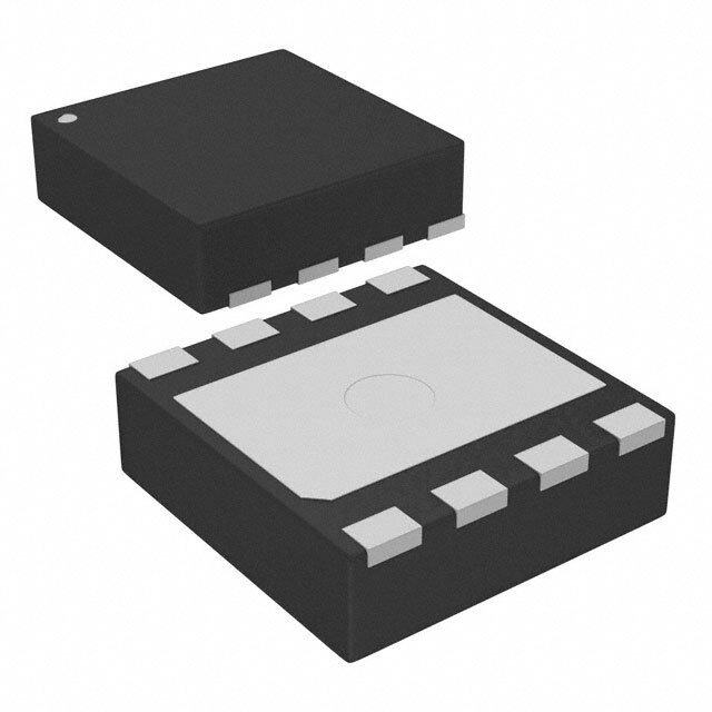
| 描述 | IC LED DRIVR WHITE BCKLGT 16-LLPLED照明驱动器 Step-Up Converter for White LED Applications 16-WQFN -40 to 125 |
| 产品分类 | |
| 品牌 | Texas Instruments |
| 产品手册 | |
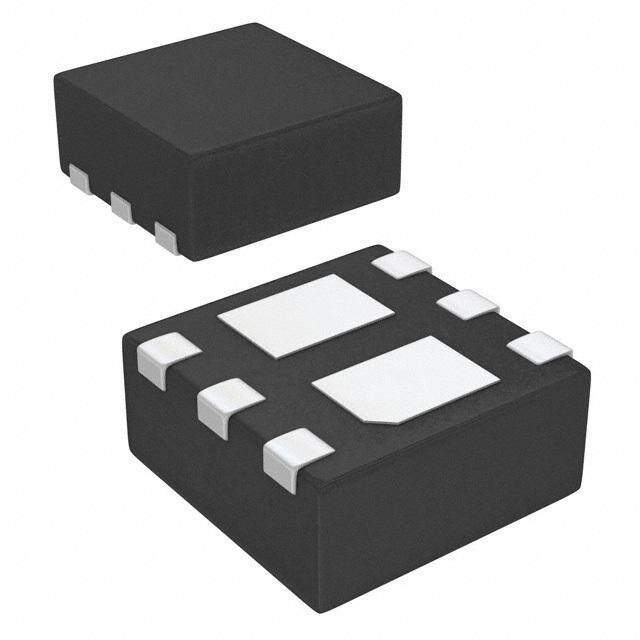
| 产品图片 |
|
| rohs | 符合RoHS无铅 / 符合限制有害物质指令(RoHS)规范要求 |
| 产品系列 | LED照明电子器件,LED照明驱动器,Texas Instruments LM3502SQ-44/NOPB- |
| 数据手册 | |
| 产品型号 | LM3502SQ-44/NOPB |
| 产品种类 | LED照明驱动器 |
| 供应商器件封装 | 16-LLP-EP(4x4) |
| 其它名称 | *LM3502SQ-44/NOPB |
| 内部驱动器 | 是 |
| 包装 | 剪切带 (CT) |
| 商标 | Texas Instruments |
| 安装类型 | 表面贴装 |
| 安装风格 | SMD/SMT |
| 宽度 | 4 mm |
| 封装 | Reel |
| 封装/外壳 | 16-WFQFN 裸露焊盘 |
| 封装/箱体 | LLP EP |
| 工作温度 | -40°C ~ 85°C |
| 工作频率 | 1 MHz |
| 工厂包装数量 | 1000 |
| 恒压 | - |
| 恒流 | - |
| 拓扑 | PWM,升压(升压) |
| 拓扑结构 | Boost |
| 最大工作温度 | + 85 C |
| 最大电源电流 | 3 mA |
| 最小工作温度 | - 40 C |
| 标准包装 | 1 |
| 电压-电源 | 2.5 V ~ 5.5 V |
| 电压-输出 | 41 V ~ 42 V |
| 类型 | Inductive |
| 类型-初级 | 背光 |
| 类型-次级 | 白色 LED |
| 系列 | LM3502 |
| 设计资源 | http://www.digikey.com/product-highlights/cn/zh/texas-instruments-webench-design-center/3176 |
| 输入电压 | 2.5 V to 5.5 V |
| 输出数 | 2 |
| 输出电流 | 750 mA |
| 输出端数量 | 2 Output |
| 输出类型 | Current Mode |
| 频率 | 800kHz ~ 1.2MHz |



- 商务部:美国ITC正式对集成电路等产品启动337调查
- 曝三星4nm工艺存在良率问题 高通将骁龙8 Gen1或转产台积电
- 太阳诱电将投资9.5亿元在常州建新厂生产MLCC 预计2023年完工
- 英特尔发布欧洲新工厂建设计划 深化IDM 2.0 战略
- 台积电先进制程称霸业界 有大客户加持明年业绩稳了
- 达到5530亿美元!SIA预计今年全球半导体销售额将创下新高
- 英特尔拟将自动驾驶子公司Mobileye上市 估值或超500亿美元
- 三星加码芯片和SET,合并消费电子和移动部门,撤换高东真等 CEO
- 三星电子宣布重大人事变动 还合并消费电子和移动部门
- 海关总署:前11个月进口集成电路产品价值2.52万亿元 增长14.8%

PDF Datasheet 数据手册内容提取
LM3502 www.ti.com SNVS339B–SEPTEMBER2005–REVISEDMAY2013 LM3502 Step-Up Converter for White LED Applications CheckforSamples:LM3502 FEATURES APPLICATIONS 1 • Driveupto4,6,8or10WhiteLEDsforDual • DualDisplayBacklightinginPortableDevices 2 DisplayBacklighting • CellularPhonesandPDAs • >80%Efficiency DESCRIPTION • OutputVoltageOptions:16V,25V,35V,and 44V The LM3502 is a white LED driver for lighting applications. For dual display or large single white • InputUnder-VoltageProtection LED string backlighting applications, the LM3502 • InternalSoftStartEliminatingInrushCurrent provides a complete solution. The LM3502 contains • 1MHzConstantSwitchingFrequency two internal white LED current bypass FET(Field Effect Transistor) switches that are ideal for • WideInputVoltage:2.5Vto5.5V controlling dual display applications. The white LED • SmallExternalComponents current can be adjusted with a PWM signal directly • LowProfilePackages:<1mmHeight from a microcontroller without the need of an RC filter – 10BumpDSBGA network. – 16PinWQFN Typical Application L 22 PH D MAIN: 2 to 5 LEDs Sw VIN VOUT1 VSUPPLY + 4.C7I NPF Cntrl VOUT2 - LM3502-44 COUT En1 Fb 1 PF En2 AGND PGND Logic SUB: Voltage 2 to 5 Signal LEDs Inputs R1 Figure1. BlacklightConfigurationwith10WhiteLEDs 1 Pleasebeawarethatanimportantnoticeconcerningavailability,standardwarranty,anduseincriticalapplicationsof TexasInstrumentssemiconductorproductsanddisclaimerstheretoappearsattheendofthisdatasheet. Alltrademarksarethepropertyoftheirrespectiveowners. 2 PRODUCTIONDATAinformationiscurrentasofpublicationdate. Copyright©2005–2013,TexasInstrumentsIncorporated Products conform to specifications per the terms of the Texas Instruments standard warranty. Production processing does not necessarilyincludetestingofallparameters.
LM3502 SNVS339B–SEPTEMBER2005–REVISEDMAY2013 www.ti.com DESCRIPTION (CONTINUED) With no external compensation, cycle-by-cycle current limit, over-voltage protection, and under-voltage protection, the LM3502 offers superior performance over other application specific standard product step-up whiteLEDdrivers. Connection Diagrams A2 4 3 2 1 A1 A3 5 16 B1 B3 6 15 7 14 C1 C3 8 13 D1 D3 9 10 11 12 D2 Figure2.TOPVIEW Figure3.TOPVIEW 10-BumpThinDSBGA 16-LeadThinWQFN SeePackageNumber(YPA0010) SeePackageNumber(RGH0016A) PINDESCRIPTIONS Bump# Pin# Name Description A1 9 Cntrl ShutdownControlConnection B1 7 Fb FeedbackVoltageConnection C1 6 V DrainConnectionsofTheNMOSandPMOSFieldEffectTransistor(FET)Switches(Figure4:N2 OUT2 andP1) D1 4 V Over-VoltageProtection(OVP)andSourceConnectionofThePMOSFETSwitch(Figure4:P1) OUT1 D2 2and3 Sw DrainConnectionofThePowerNMOSSwitch(Figure4:N1) D3 15and16 PGND PowerGroundConnection C3 14 AGND AnalogGroundConnection B3 13 V SupplyorInputVoltageConnection IN A3 12 En2 NMOSFETSwitchControlConnection A2 10 En1 PMOSFETSwitchControlConnection 1 NC NoConnection 5 NC NoConnection 8 NC NoConnection 11 NC NoConnection DAP DAP DieAttachPad(DAP),mustbesolderedtotheprintedcircuitboard’sgroundplaneforenhanced thermaldissipation. Cntrl(BumpA1): Shutdowncontrolpin WhenV is≥ 1.4V,theLM3502isenabledorON.WhenV is≤ 0.3V,theLM3502will Cntrl Cntrl enterintoshutdownmodeoperation.TheLM3502hasaninternalpulldownresistoronthe Cntrlpin,thusthedeviceisnormallyintheoffstateorshutdownmodeofoperation. Fb(BumpB1):Outputvoltagefeedbackconnection ThewhiteLEDstringnetworkcurrentisset/programmedusingaresistorfromthispinto ground. V (BumpC1): DrainconnectionsoftheinternalPMOSandNMOSFETswitches OUT2 .(Figure4:P1andN2).Itisrecommendedtoconnect100nFatV fortheLM3502-35V OUT2 2 SubmitDocumentationFeedback Copyright©2005–2013,TexasInstrumentsIncorporated ProductFolderLinks:LM3502
LM3502 www.ti.com SNVS339B–SEPTEMBER2005–REVISEDMAY2013 andLM3502-44versionsifV isnotused. OUT2 V (BumpD1):SourceconnectionoftheinternalPMOSFETswitch(Figure4:P1)andOVPsensingnode OUT1 Theoutputcapacitormustbeconnectedasclosetothedeviceaspossible,betweenthe V pinandgroundplane.AlsoconnecttheSchottkydiodeascloseaspossibletothe OUT1 V pintominimizetraceresistanceandEMIradiation. OUT1 Sw(BumpD2): DrainconnectionoftheinternalpowerNMOSFETswitch(Figure4:N1) Minimizethemetaltracelengthandmaximizethemetaltracewidthconnectedtothispinto reduceEMIradiationandtraceresistance. PGND(BumpD3):Powergroundpin Connectdirectlytothegroundplane. AGND(BumpC3): Analoggroundpin ConnecttheanaloggroundpindirectlytothePGNDpin. V (BumpB3):Supplyorinputvoltageconnectionpin IN TheC capacitorshouldbeasclosetothedeviceaspossible,betweentheV pinand IN IN groundplane. En2(BumpA3): EnablepinfortheinternalNMOSFETswitch(Figure4:N2)duringdeviceoperation WhenV is≤ 0.3V,theinternalNMOSFETswitchturnsonandtheSUBdisplayturnsoff. En2 WhenV is≥ 1.4V,theinternalNMOSFETswitchturnsoffandtheSUBdisplayturnson. En2 TheEn2pinhasaninternalpulldownresistor,thustheinternalNMOSFETswitchis normallyintheonstateofoperationwiththeSUBdisplayturnedoff. IfV andV are≤ 0.3VandV is≥ 1.4V,theLM3502willenteralowI shutdown En1 En2 Cntrl Q modeofoperationwherealltheinternalFETswitchesareoff.IfV isnotused,En2must OUT2 begroundedorfloatinganduseEn1alongwithCntrl,toenablethedevice. En1(BumpA2): EnablepinfortheinternalPMOSFETswitch(Figure4:P1)duringdeviceoperation WhenV is≤ 0.3V,theinternalPMOSFETswitchturnsonandtheMAINdisplayisturned En1 off.WhenV is≥ 1.4V,theinternalPMOSFETswitchturnsoffandtheMAINdisplayis En1 turnedon.TheEn1pinhasaninternalpulldownresistor,thustheinternalPMOSFET switchisnormallyintheonstateofoperationwiththeMAINdisplayturnedoff.IfV and En1 V are≤ 0.3VandV is≥ 1.4V,theLM3502willenteralowI shutdownmodeof En2 Cntrl Q operationwherealltheinternalFETswitchesareoff.IfV isnotused,En2mustbe OUT2 groundedanduseEn1alongwithCntrl,toenablethedevice. Thesedeviceshavelimitedbuilt-inESDprotection.Theleadsshouldbeshortedtogetherorthedeviceplacedinconductivefoam duringstorageorhandlingtopreventelectrostaticdamagetotheMOSgates. Copyright©2005–2013,TexasInstrumentsIncorporated SubmitDocumentationFeedback 3 ProductFolderLinks:LM3502
LM3502 SNVS339B–SEPTEMBER2005–REVISEDMAY2013 www.ti.com Absolute Maximum Ratings (1)(2)(3) V Pin −0.3Vto+5.5V IN SwPin −0.3Vto+48V FbPin −0.3Vto+5.5V CntrlPin −0.3Vto+5.5V V Pin −0.3Vto+48V OUT1 V Pin −0.3VtoV OUT2 OUT1 En1 −0.3Vto+5.5V En2 −0.3Vto+5.5V ContinuousPowerDissipation InternallyLimited MaximumJunctionTemperature (T +150°C J-MAX) StorageTemperatureRange −65°Cto+150°C ESDRating (4) HumanBodyModel: 2kV MachineModel: 200V (1) AllvoltagesarewithrespecttothepotentialattheGNDpin. (2) Absolutemaximumratingsindicatelimitsbeyondwhichdamagetothedevicemayoccur.Electricalcharacteristicspecificationsdonot applywhenoperatingthedeviceoutsideofitsratedoperatingconditions. (3) IfMilitary/Aerospacespecifieddevicesarerequired,pleasecontacttheTexasInstrumentsSalesOffice/Distributorsforavailabilityand specifications. (4) Thehumanbodymodelisa100pFcapacitordischargedthrougha1.5kΩresistorintoeachpin.Themachinemodelisa200pF capacitordischargeddirectlyintoeachpin. Operating Conditions (1)(2) JunctionTemperature(T)Range −40°Cto+125°C J AmbientTemperature(T )Range −40°Cto+85°C A InputVoltage,V Pin 2.5Vto5.5V IN Cntrl,En1,andEn2Pins 0Vto5.5V (1) Absolutemaximumratingsindicatelimitsbeyondwhichdamagetothedevicemayoccur.Electricalcharacteristicspecificationsdonot applywhenoperatingthedeviceoutsideofitsratedoperatingconditions. (2) AllvoltagesarewithrespecttothepotentialattheGNDpin. Thermal Properties (1) Junction-to-AmbientThermalResistance(θ ) JA DSBGAPackage 65°C/W WQFNPackage 49°C/W (1) Themaximumallowablepowerdissipationisafunctionofthemaximumjunctiontemperature,T(MAX),thejunction-to-ambientthermal J resistance,θ ,andtheambienttemperature,T .SeeThermalPropertiesforthethermalresistance.Themaximumallowablepower JA A dissipationatanyambienttemperatureiscalculatedusing:P (MAX)=(T(MAX)–T )/θ .Exceedingthemaximumallowablepower D J A JA dissipationwillcauseexcessivedietemperature.Formoreinformationonthistopic,pleaserefertoApplicationNote1187:Leadless LeadframePackage(LLP)andApplicationNote1112forDSBGAchipscalepackage. Preliminary Electrical Characteristics (1) (2) LimitsinstandardtypefaceareforT =25°C.Limitsinboldtypefaceapplyoverthefulloperatingjunctiontemperaturerange J (−40°C≤T ≤+125°C).Unlessotherwisespecified,V =2.5V. J IN Symbol Parameter Conditions Min Typ Max Units V InputVoltage 2.5 5.5 V IN I Non-Switching Fb>0.25V 0.5 1 mA Q Switching Fb=0V,SwIsFloating 1.9 3 mA Shutdown Cntrl=0V 0.1 3 µA LowI Shutdown Cntrl=1.5V,En1=En2=0V 6 15 µA Q V FeedbackVoltage 0.18 0.25 0.3 V Fb (1) AllvoltagesarewithrespecttothepotentialattheGNDpin. (2) MinandMaxlimitsareensuredbydesign,test,orstatisticalanalysis.Typicalnumbersarenotensured,butdorepresentthemostlikely norm. 4 SubmitDocumentationFeedback Copyright©2005–2013,TexasInstrumentsIncorporated ProductFolderLinks:LM3502
LM3502 www.ti.com SNVS339B–SEPTEMBER2005–REVISEDMAY2013 Preliminary Electrical Characteristics (1) (2) (continued) LimitsinstandardtypefaceareforT =25°C.Limitsinboldtypefaceapplyoverthefulloperatingjunctiontemperaturerange J (−40°C≤T ≤+125°C).Unlessotherwisespecified,V =2.5V. J IN Symbol Parameter Conditions Min Typ Max Units I NMOSPowerSwitch −16,Fb=0V 250 400 650 CL CurrentLimit −25,Fb=0V 400 600 800 mA −35,Fb=0V 450 750 1050 −44,Fb=0V 450 750 1050 I FeedbackPinBias Fb=0.25V Fb Current (3) 64 500 nA F SwitchingFrequency 0.8 1 1.2 MHz S R NMOSPowerSwitchON I =500mA DS(ON) Sw Resistance 0.55 1.1 Ω (Figure4:N1) R PMOSONResistanceof I =20mA,En1=0V,En2=1.5V PDS(ON) PMOS V /V Switch 5 10 Ω OUT1 OUT2 (Figure4:N1) R NMOSONResistanceof I =20mA,En1=1.5V,En2=0V NDS(ON) NMOS V /FbSwitch 2.5 5 Ω OUT2 (Figure4:N2) D MaximumDutyCycle Fb=0V 90 95 % MAX I CntrlPinInputBias Cntrl=2.5V 7 14 Cntrl Current (4) Cntrl=0V 0.1 µA I SwPinLeakageCurrent Sw=42V,Cntrl=0V Sw (5) 0.01 5 µA I V PinLeakage V =14V,Cntrl=0V(16) 0.1 3 VOUT1(OFF) OUT1 OUT1 Current (5) V =23V,Cntrl=0V(25) 0.1 3 OUT1 µA V =32V,Cntrl=0V(35) 0.1 3 OUT1 V =42V,Cntrl=0V(44) 0.1 3 OUT1 I V PinBiasCurrent V =14V,Cntrl=1.5V(16) 40 80 VOUT1(ON) OUT1 OUT1 (5) V =23V,Cntrl=1.5V(25) 50 100 OUT1 µA V =32V,Cntrl=1.5V(35) 50 100 OUT1 V =42V,Cntrl=1.5V(44) 85 140 OUT1 I V PinLeakage Fb=0V,Cntrl=0V,V =42V VOUT2 COuUrrTe2nt (5) OUT2 0.1 3 µA UVP Under-Voltage OnThreshold 2.4 2.5 V Protection OffThreshold 2.2 2.3 OVP Over-VoltageProtection OnThreshold(16) 14.5 15.5 16.5 (6) OffThreshold(16) 14.0 15 16.0 OnThreshold(25) 22.5 24 25.5 OffThreshold(25) 21.5 23 24.5 V OnThreshold(35) 32.0 34 35.0 OffThreshold(35) 31.0 33 34.0 OnThreshold(44) 40.5 42 43.5 OffThreshold(44) 39.0 41 42.0 V PMOSFETSwitch OffThreshold(DisplayLighting) 0.8 0.3 En1 EnablingThreshold OnThreshold(DisplayLighting) 1.4 0.8 V (Figure4:P1) V NMOSFETSwitch OffThreshold(DisplayLighting) 0.8 0.3 En2 EnablingThreshold OnThreshold(DisplayLighting) 1.4 0.8 V (Figure4:N2) V DeviceEnabling OffThreshold 0.8 0.3 Cntrl V Threshold OnThreshold 1.4 0.8 T ShutdownDelayTime 8 12 16 ms SHDW I En1PinInputBias En1=2.5V 7 14 En1 µA Current En1=0V 0.1 (3) Currentflowsoutofthepin. (4) Currentflowsintothepin. (5) Currentflowsintothepin. (6) TheonthresholdindicatesthattheLM3502isnolongerswitchingorregulatingLEDcurrent,whiletheoffthresholdindicatesnormal operation. Copyright©2005–2013,TexasInstrumentsIncorporated SubmitDocumentationFeedback 5 ProductFolderLinks:LM3502
LM3502 SNVS339B–SEPTEMBER2005–REVISEDMAY2013 www.ti.com Preliminary Electrical Characteristics (1) (2) (continued) LimitsinstandardtypefaceareforT =25°C.Limitsinboldtypefaceapplyoverthefulloperatingjunctiontemperaturerange J (−40°C≤T ≤+125°C).Unlessotherwisespecified,V =2.5V. J IN Symbol Parameter Conditions Min Typ Max Units I En2PinInputBias En2=2.5V 7 14 En2 µA Current En2=0V 0.1 BLOCK DIAGRAM 13 VIN 2,3 Sw Soft Start Thermal Shutdown Current Limit OVP Comparator VOUT1 + UVP - 4 Comparator UVP - OVP Reference + Reference Light Load Light Load Reference + Comparator Current Sense - Error Amplifier PWM Fb Comparator P1 - - N1 + + Driver Logic Fb Reference VOUT2 N2 6 Oscillator FET Logic Duty Limit Shutdown Comparator Comparator + - Duty Limit Reference 7 14 9 15,16 10 12 En2 Fb AGND Cntrl PGND En1 Figure4. BlockDiagram Detailed Description of Operation The LM3502 utilizes an asynchronous current mode pulse-width-modulation (PWM) control scheme to regulate the feedback voltage over specified load conditions. The DC/DC converter behaves as a controlled current source for white LED applications. The operation can best be understood by referring to the block diagram in Figure 4 for the following operational explanation. At the start of each cycle, the oscillator sets the driver logic and turns on the internal NMOS power device, N1, conducting current through the inductor and reverse biasing the external diode. The white LED current is supplied by the output capacitor when the internal NMOS power device, N1, is turned on. The sum of the error amplifier’s output voltage and an internal voltage ramp are compared with the sensed power NMOS, N1, switch voltage. Once these voltages are equal, the PWM 6 SubmitDocumentationFeedback Copyright©2005–2013,TexasInstrumentsIncorporated ProductFolderLinks:LM3502
LM3502 www.ti.com SNVS339B–SEPTEMBER2005–REVISEDMAY2013 comparator will then reset the driver logic, thus turning off the internal NMOS power device, N1, and forward biasing the external diode. The inductor current then flows through the diode to the white LED load and output capacitor. The inductor current recharges the output capacitor and supplies the current for the white LED load. The oscillator then resets the driver logic again repeating the process. The output voltage of the error amplifier controls the current through the inductor. This voltage will increase for larger loads and decrease for smaller loads limiting the peak current in the inductor and minimizing EMI radiation. The duty limit comparator is always operational, it prevents the internal NMOS power switch, N1, from being on for more than one oscillator cycle and conducting large amounts of current. The light load comparator allows the LM3502 to properly regulate light/small white LED load currents, where regulation becomes difficult for the LM3502’s primary control loop. Underlightloadconditions,theLM3502willenterintoapulseskippingpulse-frequency-mode(PFM)ofoperation wheretheswitchingfrequencywillvarywiththeload. The LM3502 has 2 control pins, En1 and En2, used for selecting which segment of a single white LED string network is active for dual display applications. En1 controls the main display (MAIN) segment of the single string white LED network between pins V and V . En2 controls the sub display (SUB) segment of the single OUT1 OUT2 string white LED network between the V and Fb. For a quick review of the LM3502 control pin operational OUT2 characteristics,seeFigure5. When the Cntrl pin is ≥ 1.4V, the LM3502 will enter in low I state if both En1 and En2 ≤ 0.3V. At this time, both Q the P1 and N2 FETs will turn off. The output voltage will be a diode drop below the supply voltage and the soft- startwillberesetlimitingthepeakinductorcurrentatthenextstart-up. The LM3502 is designed to control the LED current with a PWM signal without the use of an external RC filter. Utilizing special circuitry, the LM3502 can operate over a large range of PWM frequencies without restarting the soft-start allowing for fast recovery at high PWM frequencies. Figure 6 represents a PWM signal driving the Cntrl pinwheret isdefinedasthelowtimeofthesignal.Thefollowingistrue: L • Ift <12ms(typical):Thedevicewillstopswitchingduringthistimeandthesoft-startwillnotberesetallowing L LEDcurrentPWMcontrol. • Ift >12ms(typical):Thedevicewillshutdownandthesoft-startwillresettopreventhighpeakcurrentsatthe L nextstartup.BoththeN2andP1switcheswillturnoff. The LM3502 has dedicated protection circuitry active during normal operation to protect the integrated circuit (IC) and external components. The thermal shutdown circuitry turns off the internal NMOS power device, N1, when the internal semiconductor junction temperature reaches excessive levels. The LM3502 has a under-voltage protection (UVP) comparator that disables the internal NMOS power device when battery voltages are too low, thuspreventinganonstatewheretheinternalNMOSpowerdeviceconductslargeamountsofcurrent.Theover- voltage protection (OVP) comparator prevents the output voltage from increasing beyond the protection limit when the white LED string network is removed or if there is a white LED failure. OVP allows for the use of low profile ceramic capacitors at the output. The current though the internal NMOS power device, N1, is monitored to prevent peak inductor currents from damaging the IC. If during a cycle (cycle=1/switching frequency) the peak inductor current exceeds the current limit for the LM3502, the internal NMOS power device will be turned off for theremainingdurationofthatcycle. Copyright©2005–2013,TexasInstrumentsIncorporated SubmitDocumentationFeedback 7 ProductFolderLinks:LM3502
LM3502 SNVS339B–SEPTEMBER2005–REVISEDMAY2013 www.ti.com Shutdown Cntrl* En1 En2 Result* (See Figure 1 and Figure 2) Shutdown Low IQ 1.4V 0.3V 0.3V [P1˘OFF N2˘OFF N1˘OFF] or [MAIN˘OFF SUB˘OFF N1˘OFF] X 1.4V 1.4V 0.3V [P1˘OFF N2˘ON N1˘Switching] or [MAIN˘ON SUB˘OFF N1˘Switching] 1.4V 0.3V 1.4V [P1˘ON N2˘OFF N1˘Switching] or [MAIN˘OFF SUB˘ON N1˘Switching] 1.4V 1.4V 1.4V [P1˘OFF N2˘OFF N1˘Switching] or [MAIN˘ON SUB˘ON N1˘Switching] 0.3V 0.3V 0.3V [P1˘OFF N2˘OFF N1˘OFF] or [MAIN˘OFF SUB˘OFF N1˘OFF] X 0.3V 1.4V 0.3V [P1˘OFF N2˘OFF N1˘OFF] or [MAIN˘OFF SUB˘OFF N1˘OFF] X 0.3V 0.3V 1.4V [P1˘OFF N2˘OFF N1˘OFF] or [MAIN˘OFF SUB˘OFF N1˘OFF] X 0.3V 1.4V 1.4V [P1˘OFF N2˘OFF N1˘OFF] or [MAIN˘OFF SUB˘OFF N1˘OFF] X *Table is only valid for when the Cntrl pin signal is a non-periodic logic signal, not a PWM signal. Figure5. OperationalCharacteristicsTable 1.4V Cntrl 0.3V tL (Typ) Figure6. ControlSignalWaveform 8 SubmitDocumentationFeedback Copyright©2005–2013,TexasInstrumentsIncorporated ProductFolderLinks:LM3502
LM3502 www.ti.com SNVS339B–SEPTEMBER2005–REVISEDMAY2013 Typical Performance Characteristics (CircuitinFigure1:L=DO1608C-223andD=MBRM140T3.Efficiency:η=P /P =[(V –V )*I ]/[V *I ].T = OUT IN OUT Fb OUT IN IN A 25°C,unlessotherwisestated.) I (Non-Switching) SwitchingFrequency Q vs vs V Temperature IN 0.600 1.03 0.580 1.02 VIN = 2.5V )A 0.560 -40oC 1.01 m( I GNIHQ 000...555204000 25oC 125oC )zHM( YCN 100...099089 C E TIW 0.480 UQ 0.97 S-N 0.460 ERF 0.96 O N 0.440 0.95 0.420 0.94 0.400 0.93 2.5 3.0 3.5 4.0 4.5 5.0 5.5 -40 -20 0 20 40 60 80 100 120 -30 -10 10 30 50 70 90 110 130 INPUT VOLTAGE (V) TEMPERATURE (oC) Figure7. Figure8. I (Switching) I (Switching) Q Q vs vs V Temperature IN 4.00 1.95 3.50 VIN = 2.5V 1.90 )Am -40oC )Am ( Q 3.00 ( Q I GN I GN 1.85 IH 25oC 125oC IH C 2.50 C T T IW IW S S 1.80 2.00 1.50 1.75 2.5 3.0 3.5 4.0 4.5 5.0 5.5 -40 -20 0 20 40 60 80 100 120 -30 -10 10 30 50 70 90 110 130 INPUT VOLTAGE (V) TEMPERATURE (oC) Figure9. Figure10. 10LEDEfficiency 8LEDEfficiency vs vs LEDCurrent LEDCurrent 90 90 VIN = 5.5V VIN = 4.2V 85 85 VIN = 5.5V 80 VIN = 4.2V 80 VIN = 3.3V )% 75 )% 75 ( Y 70 ( Y 70 CNE 65 VIN = 3.3V CNE 65 VIN = 3V ICIFFE 5650 VIN = 2.7V VIN = 3V ICIFFE 5650 VIN = 2.7V 50 50 45 45 40 40 2 12 22 32 42 52 62 2.5 7.5 12.5 17.5 22.5 27.5 32.5 5.0 10.0 15.0 20.0 25.0 30.0 35.0 LED CURRENT (mA) LED CURRENT (mA) Figure11. Figure12. Copyright©2005–2013,TexasInstrumentsIncorporated SubmitDocumentationFeedback 9 ProductFolderLinks:LM3502
LM3502 SNVS339B–SEPTEMBER2005–REVISEDMAY2013 www.ti.com Typical Performance Characteristics (continued) (CircuitinFigure1:L=DO1608C-223andD=MBRM140T3.Efficiency:η=P /P =[(V –V )*I ]/[V *I ].T = OUT IN OUT Fb OUT IN IN A 25°C,unlessotherwisestated.) 6LEDEfficiency 4LEDEfficiency vs vs LEDCurrent LEDCurrent 95 95 90 VIN = 5.5V 90 VIN = 5.5V 85 )% )% ( YCN 80 ( YCN 85 VIN = 4.2V EICIF 75 VIN = V3I.N3V = 4.2V EICIF 80 F F E 70 VIN = 3V E VIN = 2.7V 75 VIN = 2.7V VIN = 3.3V 65 60 70 2 12 22 32 42 52 62 72 82 2 10 18 26 34 42 50 58 66 74 LED CURRENT (mA) LED CURRENT (mA) Figure13. Figure14. CntrlPinCurrent MaximumDutyCycle vs vs CntrlPinVoltage Temperature 30 98 )A 25 VIN = 2.5 ( TNP 20 -40oC )%( E 97 E L R C R Y UC N 15 25oC C YT 96 IP LRTN 10 125oC UD XAM 95 C 5 0 94 0.0 1.0 2.0 3.0 4.0 5.0 -40 -20 0 20 40 60 80 100 120 -30 -10 10 30 50 70 90 110 130 CNTRL PIN VOLTAGE (V) TEMPERATURE (oC) Figure15. Figure16. En1PinCurrent En2PinCurrent vs vs En1PinVoltage En2PinVoltage 30 25 25 20 )A )A ( TNEP 20 -40oC ( TNEP 15 RRU 15 RRU -40oC C NIP 10 25oC C NIP 10 25oC 1NE 125oC 2NE 5 125oC 5 0 0 0.0 1.0 2.0 3.0 4.0 5.0 0.0 1.0 2.0 3.0 4.0 5.0 EN1 PIN VOLTAGE (V) EN2 PIN VOLTAGE (V) Figure17. Figure18. 10 SubmitDocumentationFeedback Copyright©2005–2013,TexasInstrumentsIncorporated ProductFolderLinks:LM3502
LM3502 www.ti.com SNVS339B–SEPTEMBER2005–REVISEDMAY2013 Typical Performance Characteristics (continued) (CircuitinFigure1:L=DO1608C-223andD=MBRM140T3.Efficiency:η=P /P =[(V –V )*I ]/[V *I ].T = OUT IN OUT Fb OUT IN IN A 25°C,unlessotherwisestated.) V PinCurrent PowerNMOSR (Figure4:N1) OUT1 DS(ON) vs vs V PinVoltage V OUT1 IN 160 1000 INMOS = 400 mA )AP 140 :) 900 ( TNERR 110200 -40oC m( )NO(S 800 125oC UC SAIB NIP 1TU 468000 25oC 125oC R SOMN REWOD 567000000 25oC VO 20 P 400 -40oC 0 300 0 8 16 24 32 40 48 2.5 3.0 3.5 4.0 4.5 5.0 5.5 VOUT1 PIN VOLTAGE (V) INPUT VOLTAGE (V) Figure19. Figure20. NMOSR (Figure4:N2) PMOSR (Figure4:P1) DS(ON) DS(ON) vs vs V V IN IN 3.50 10 INMOS = 20 mA IPMOS = 20 mA 3.00 9 :) :) ( )NO 2.50 125oC ( )NO 8 125oC (S (S RD 2.00 RD 7 H H C C TIW 1.50 25oC TIW 6 S S 25oC SO 1.00 -40oC SO 5 M M N P 0.50 4 -40oC 0.00 3 2.5 3.0 3.5 4.0 4.5 5.0 5.5 2.0 12.0 22.0 32.0 42.0 INPUT VOLTAGE (V) VOUT1 PIN VOLTAGE (V) Figure21. Figure22. FeedbackVoltage CurrentLimit(LM3502-16) vs vs Temperature V IN 480 460 )Am 440 ( T T = 85oC IM 420 IL TNE 400 T = 25oC R R 380 U C 6 360 1- T = -40oC 340 320 2.5 3.0 3.5 4.0 4.5 5.0 5.5 INPUT VOLTAGE (V) Figure23. Figure24. Copyright©2005–2013,TexasInstrumentsIncorporated SubmitDocumentationFeedback 11 ProductFolderLinks:LM3502
LM3502 SNVS339B–SEPTEMBER2005–REVISEDMAY2013 www.ti.com Typical Performance Characteristics (continued) (CircuitinFigure1:L=DO1608C-223andD=MBRM140T3.Efficiency:η=P /P =[(V –V )*I ]/[V *I ].T = OUT IN OUT Fb OUT IN IN A 25°C,unlessotherwisestated.) CurrentLimit(LM3502-16) CurrentLimit(LM3502-25) vs vs Temperature V IN 440 620 T = 85oC 600 420 )A VIN = 2.5V )A 580 m( T 400 m( T 560 T = 25oC IM IM IL T 380 VIN = 5.5V IL T 540 N N E E 520 R R R R U 360 U 500 C 61 C 52 480 T = -40oC - 340 - 460 320 440 -40 -25 -10 5 20 35 50 65 80 2.5 3.0 3.5 4.0 4.5 5.0 5.5 TEMPERATURE (oC) INPUT VOLTAGE (V) Figure25. Figure26. CurrentLimit(LM3502-25) CurrentLimit(LM3502-35/44) vs vs Temperature Temperature 620 780 600 VIN = 2.5V 770 )A 580 )Am 760 m( TIMIL TN 555624000 VIN = 5.5V ( TIMIL TNE 774500 E R 730 R 500 R R U U C 720 C 52- 446800 44/53 710 VIN = 2.5V - 440 700 420 690 -40 -25 -10 5 20 35 50 65 80 -40 -25 -10 5 20 35 50 65 80 TEMPERATURE (oC) TEMPERATURE (oC) Figure27. Figure28. CurrentLimit(LM3502-35/44) vs V IN 780 770 760 )A 85oC m 750 ( T IM 740 IL TN 730 25oC -40oC E R R 720 U C 710 700 690 2.5 3.0 3.5 4.0 4.5 5.0 5.5 INPUT VOLTAGE (V) Figure29. 12 SubmitDocumentationFeedback Copyright©2005–2013,TexasInstrumentsIncorporated ProductFolderLinks:LM3502
LM3502 www.ti.com SNVS339B–SEPTEMBER2005–REVISEDMAY2013 APPLICATION INFORMATION WHITE LED CURRENT SETTING TheLEDcurrentissetusingthefollowingequation: V Fb I = LED R1 where • I :WhiteLEDCurrent. LED • V :FeedbackPinVoltage.V =0.25V,Typical. Fb Fb • R1:CurrentSettingResistor. (1) WHITE LED DIMMING For dimming the white LED string with a pulse-width-modulated (PWM) signal on the Cntrl pin, care must taken to balance the tradeoffs between audible noise and white LED brightness control. For best PWM duty cycle vs. white LED current linearity, the PWM frequency should be between 200Hz and 500Hz. Other PWM frequencies canbeused,butthelinearityoverinputvoltageanddutycyclevariationwillnotbeasgoodaswhatthe200Hzto 500Hz PWM frequency spectrum provides. To minimize audible noise interference, it is recommended that a output capacitor with minimal susceptibility to piezoelectric induced stresses be used for the particular applicationsthatrequireminimalornoaudiblenoiseinterference. PWM Signal VSUPPLY Sw VIN VOUT1 Unconnected Cntrl VOUT2 Floating LM3502 En1 Fb GND En2 AGND PGND R1 Figure30. IfV isnotused,En2mustbegrounded OUT2 Copyright©2005–2013,TexasInstrumentsIncorporated SubmitDocumentationFeedback 13 ProductFolderLinks:LM3502
LM3502 SNVS339B–SEPTEMBER2005–REVISEDMAY2013 www.ti.com tON= DTS nt e urr C or (Vin - Vout)/L ct Vin/L u nd IL(avg) I 'iL Time TS Figure31. InductorCurrentWaveform CONTINUOUS AND DISCONTINUOUS MODES OF OPERATION Since the LM3502 is a constant frequency pulse-width-modulated step-up regulator, care must be taken to make sure the maximum duty cycle specification is not violated. The duty cycle equation depends on which mode of operation the LM3502 is in. The two operational modes of the LM3502 are continuous conduction mode (CCM) and discontinuous conduction mode (DCM). Continuous conduction mode refers to the mode of operation where during the switching cycle, the inductor current never goes to and stays at zero for any significant amount of time during the switching cycle. Discontinuous conduction mode refers to the mode of operation where during the switching cycle, the inductor current goes to and stays at zero for a significant amount of time during the switching cycle. Figure 31 illustrates the threshold between CCM and DCM operation. In Figure 31, the inductor current is right on the CCM/DCM operational threshold. Using this as a reference, a factor can be introduced to calculate when a particular application is in CCM or DCM operation. R is a CCM/DCM factor we can use to compute which mode of operation a particular application is in. If R is ≥ 1, then the application is operating in CCM. Conversely, if R is < 1, the application is operating in DCM. The R factor inequalities are a result of the components that make up the R factor. From Figure 31, the R factor is equal to the average inductor current, I (avg), divided by half the inductor ripple current, Δi . Using Figure 31 the following equation can be used to L L computeRfactor: 2 * I (avg) L R = ’i L [I ] OUT I (avg) = L [(1-D) * Eff] [V * D] IN ’i = L [L * Fs] 2 [2 * I * L * Fs * (V ) ] OUT OUT R = 2 [(V ) * Eff * (V - V )] IN OUT IN where • V :InputVoltage. IN • V :OutputVoltage. OUT • Eff:EfficiencyoftheLM3502. • Fs:SwitchingFrequency. • I :WhiteLEDCurrent/LoadCurrent. OUT • L:InductanceMagnitude/InductorValue. • D:DutyCycleforCCMOperation. • Δi :InductorRippleCurrent L • I (avg):AverageInductorCurrent (2) L ForCCMoperation,thedutycyclecanbecomputedwith: 14 SubmitDocumentationFeedback Copyright©2005–2013,TexasInstrumentsIncorporated ProductFolderLinks:LM3502
LM3502 www.ti.com SNVS339B–SEPTEMBER2005–REVISEDMAY2013 t ON D = T S [V - V ] OUT IN D = [V ] OUT where • D:DutyCycleforCCMOperation. • V :OutputVoltage. OUT • V :InputVoltage. (3) IN ForDCMoperation,thedutycyclecanbecomputedwith: t ON D = T S [2 * I * L * (V - V ) * Fs] OUT OUT IN D = 2 [(V ) * Eff] IN where • D:DutyCycleforDCMOperation. • V :OutputVoltage. OUT • V :InputVoltage. IN • I :WhiteLEDCurrent/LoadCurrent. OUT • Fs:SwitchingFrequency. • L:InductorValue/InductanceMagnitude. (4) INDUCTOR SELECTION In order to maintain inductance, an inductor used with the LM3502 should have a saturation current rating larger than the peak inductor current of the particular application. Inductors with low DCR values contribute decreased power losses and increased efficiency. The peak inductor current can be computed for both modes of operation: CCMandDCM. Thecycle-by-cyclepeakinductorcurrentforCCMoperationcanbecomputedwith: ’i | L I I (avg) + Peak L 2 | [IOUT] [VIN * D] I + Peak [(1 - D) * Eff] [2 * L * Fs] where • V :InputVoltage. IN • Eff:EfficiencyoftheLM3502. • Fs:SwitchingFrequency. • I :WhiteLEDCurrent/LoadCurrent. OUT • L:InductanceMagnitude/InductorValue. • D:DutyCycleforCCMOperation. • I :PeakInductorCurrent. PEAK • Δi :InductorRippleCurrent. L • I (avg):AverageInductorCurrent. (5) L Thecycle-by-cyclepeakinductorcurrentforDCMoperationcanbecomputedwith: [V * D] | IN I Peak [L * Fs] where • V :InputVoltage. IN Copyright©2005–2013,TexasInstrumentsIncorporated SubmitDocumentationFeedback 15 ProductFolderLinks:LM3502
LM3502 SNVS339B–SEPTEMBER2005–REVISEDMAY2013 www.ti.com • Fs:SwitchingFrequency. • L:InductanceMagnitude/InductorValue. • D:DutyCycleforDCMOperation. • I :PeakInductorCurrent. (6) PEAK The minimum inductance magnitude/inductor value for the LM3502 can be calculated using the following, which isonlyvalidwhenthedutycycleis>0.5: [V * R * ((D/’¶) - 1)] IN DS(ON) L > [1.562 * Fs] where • D:DutyCycle. • D:1–D. • R :NMOSPowerSwitchON DS(ON) • V :InputVoltage. IN • L:InductanceMagnitude/InductorValue. (7) This equation gives the value required to prevent subharmonic oscillations. The result of this equation and the inductoraverageandripplecurrentshouldbeaccountedforwhenchoosinganinductorvalue. Somerecommendedinductormanufacturersincludedbutarenotlimitedto: DO1608C-223 CoilCraft www.coilcraft.com DT1608C-223 CAPACITOR SELECTION Multilayer ceramic capacitors are the best choice for use with the LM3502. Multilayer ceramic capacitors have the lowest equivalent series resistance (ESR). Applied voltage or DC bias, temperature, dielectric material type (X7R, X5R, Y5V, etc), and manufacturer component tolerance have an affect on the true or effective capacitance of a ceramic capacitor. Be aware of how your application will affect a particular ceramic capacitor by analyzing the aforementioned factors of your application. Before selecting a capacitor always consult the capacitor manufacturer’sdatacurvestoverifytheeffectiveortruecapacitanceinyourapplication. INPUT CAPACITOR SELECTION Theinputcapacitorservesasanenergyreservoirfortheinductor.Inadditiontoactingasanenergyreservoirfor the inductor the input capacitor is necessary for the reduction in input voltage ripple and noise experienced by the LM3502. The reduction in input voltage ripple and noise helps ensure the LM3502’s proper operation, and reduces the effect of the LM3502 on other devices sharing the same supply voltage. To ensure low input voltage ripple, the input capacitor must have an extremely low ESR. As a result of the low input voltage ripple requirement multilayer ceramic capacitors are the best choice. A minimum capacitance of 2.0 µF is required for normal operation, so consult the capacitor manufacturer’s data curves to verify whether the minimum capacitancerequirementisgoingtobeachievedforaparticularapplication. OUTPUT CAPACITOR SELECTION The output capacitor serves as an energy reservoir for the white LED load when the internal power FET switch (Figure 4: N1) is on or conducting current. The requirements for the output capacitor must include worst case operation such as when the load opens up and the LM3502 operates in over-voltage protection (OVP) mode operation. A minimum capacitance of 0.5µF is required to ensure normal operation. Consult the capacitor manufacturer’s data curves to verify whether the minimum capacitance requirement is going to be achieved for a particularapplication. Somerecommendedcapacitormanufacturersincludedbutarenotlimitedto: Taiyo GMK212BJ105MD www.t-yuden.com Yuden (0805/35V) muRata GRM40-035X7R105K www.murata.com (0805/50V) 16 SubmitDocumentationFeedback Copyright©2005–2013,TexasInstrumentsIncorporated ProductFolderLinks:LM3502
LM3502 www.ti.com SNVS339B–SEPTEMBER2005–REVISEDMAY2013 TDK C3216X7R1H105KT www.tdktca.com (1206/50V) C3216X7R1C475K (1206/16V) AVX 08053D105MAT www.avxcorp.com (0805/25V) 08056D475KAT (0805/6.3V) 1206ZD475MAT (1206/10V) DIODE SELECTION To maintain high efficiency it is recommended that the average current rating (I or I ) of the selected diode F O should be larger than the peak inductor current (I ). At the minimum, the average current rating of the diode Lpeak should be larger than the maximum LED current. To maintain diode integrity the peak repetitive forward current (I ) must be greater than or equal to the peak inductor current (I ). Diodes with low forward voltage ratings FRM Lpeak (V ) and low junction capacitance magnitudes (C or C or C ) are conducive to high efficiency. The chosen F J T D diode must have a reverse breakdown voltage rating (V and/or V ) that is larger than the output voltage R RRM (V ).Nomatterwhattypeofdiodeischosen,Schottkyornot,certainselectioncriteriamustbefollowed: out 1. V andV >V R RRM OUT 2. I orI ≥I orI F O LOAD OUT 3. I ≥I FRM Lpeak Somerecommendeddiodemanufacturersincludedbutarenotlimitedto: Vishay SS12(1A/20V) www.vishay.com SS14(1A/40V) SS16(1A/60V) On MBRM120E www.onsemi.com Semiconductor (1A/20V) MBRS1540T3 (1.5A/40V) MBR240LT (2A/40V) Central CMSH1-40M www.centralsemi.com Semiconductor (1A/40V) SHUTDOWN AND START-UP On startup, the LM3502 contains special circuitry that limits the peak inductor current which prevents large current spikes from loading the battery or power supply. When Cntrl ≥ 1.4V and both the En1 and En2 signals are less than 0.3V, the LM3502 will enter a low I state and regulation will end. During this low I mode the Q Q output voltage is a diode drop below the supply voltage and the soft-start will be reset to limit the peak inductor current at the next startup. When both En1 and En2 are less than 0.3V, the P1 PMOS and N2 NMOS switches willturnoff. WhenCntrl<0.3Vformorethan12ms,typicaly,theLM3502willshutdownandtheoutputvoltagewillbeadiode drop below the supply voltage. If the Cntrl pin is low for more than 12ms, the soft-start will reset to limit the peak inductorcurrentatthenextstartup. WhenCntrlis<0.3butforlessthan12ms,typically,thedevicewillnotshutdownandresetthesoft-startbutshut offtheNMOSN1PowerDevicetoallowforPWMcontrloftheLEDcurrent. THERMAL SHUTDOWN The LM3502 stops regulating when the internal semiconductor junction temperature reaches approximately 140°C. The internal thermal shutdown has approximately 20°C of hysteresis which results in the LM3502 turning back on when the internal semiconductor junction temperature reaches 120°C. When the thermal shutdown temperatureisreached,thesoftstartisresettopreventinrushcurrentwhenthedietemperaturecools. Copyright©2005–2013,TexasInstrumentsIncorporated SubmitDocumentationFeedback 17 ProductFolderLinks:LM3502
LM3502 SNVS339B–SEPTEMBER2005–REVISEDMAY2013 www.ti.com UNDER VOLTAGE PROTECTION The LM3502 contains protection circuitry to prevent operation for low input supply voltages. When Vin drops below 2.3V, typically the LM3502 will no longer regulate. In this mode, the output volage will be one diode drop below Vin and the softstart will be reset. When Vin increases above 2.4V, typically, the device will begin regulatingagain. OVER VOLTAGE PROTECTION The LM3502 contains dedicated circuitry for monitoring the output voltage. In the event that the LED network is disconnectedfromtheLM3502,theoutputvoltagewillincreaseandbelimitedto15.5V(typ.)forthe16Vversion, 24V(typ.) for the 25V version, 34V(typ.) for the 35V version and 42V(typ.) for the 44V version (see eletrical table for more details). In the event that the network is reconnected, regulation will resume at the appropriate output voltage. LAYOUT CONSIDERATIONS All components, except for the white LEDs, must be placed as close as possible to the LM3502. The die attach pad(DAP)mustbesolderedtothegroundplane. The input bypass capacitor C , as shown in Figure 1, must be placed close to the IC and connect between the IN V and PGND pins. This will reduce copper trace resistance which effects input voltage ripple of the IC. For IN additional input voltage filtering, a 100nF bypass capacitor can be placed in parallel with C to shunt any high IN frequency noise to ground. The output capacitor, C , must be placed close to the IC and be connected OUT between the V and PGND pins. Any copper trace connections for the C capacitor can increase the series OUT1 OUT resistance, which directly effects output voltage ripple and efficiency. The current setting resistor, R1, should be kept close to the Fb pin to minimize copper trace connections that can inject noise into the system. The ground connection for the current setting resistor network should connect directly to the PGND pin. The AGND pin should be tied directly to the PGND pin. Trace connections made to the inductor should be minimized to reduce power dissipation and increase overall efficiency while reducing EMI radiation. For more details regarding layout guidelinesforswitchingregulators,refertoApplicationsNoteAN-1149. 18 SubmitDocumentationFeedback Copyright©2005–2013,TexasInstrumentsIncorporated ProductFolderLinks:LM3502
LM3502 www.ti.com SNVS339B–SEPTEMBER2005–REVISEDMAY2013 REVISION HISTORY ChangesfromRevisionA(May2013)toRevisionB Page • ChangedlayoutofNationalDataSheettoTIformat.......................................................................................................... 18 Copyright©2005–2013,TexasInstrumentsIncorporated SubmitDocumentationFeedback 19 ProductFolderLinks:LM3502
PACKAGE OPTION ADDENDUM www.ti.com 16-Oct-2015 PACKAGING INFORMATION Orderable Device Status Package Type Package Pins Package Eco Plan Lead/Ball Finish MSL Peak Temp Op Temp (°C) Device Marking Samples (1) Drawing Qty (2) (6) (3) (4/5) LM3502ITL-16/NOPB LIFEBUY DSBGA YPA 10 250 Green (RoHS SNAGCU Level-1-260C-UNLIM -40 to 125 SANB & no Sb/Br) LM3502ITL-25/NOPB LIFEBUY DSBGA YPA 10 250 Green (RoHS SNAGCU Level-1-260C-UNLIM -40 to 125 SAPB & no Sb/Br) LM3502ITL-44/NOPB LIFEBUY DSBGA YPA 10 250 Green (RoHS SNAGCU Level-1-260C-UNLIM -40 to 125 SDLB & no Sb/Br) LM3502SQ-16/NOPB LIFEBUY WQFN RGH 16 1000 Green (RoHS CU SN Level-1-260C-UNLIM -40 to 125 L00048B & no Sb/Br) LM3502SQ-25/NOPB LIFEBUY WQFN RGH 16 1000 Green (RoHS CU SN Level-1-260C-UNLIM -40 to 125 L00049B & no Sb/Br) LM3502SQ-35/NOPB LIFEBUY WQFN RGH 16 1000 Green (RoHS CU SN Level-1-260C-UNLIM -40 to 125 L00044B & no Sb/Br) LM3502SQ-44/NOPB LIFEBUY WQFN RGH 16 1000 Green (RoHS CU SN Level-1-260C-UNLIM -40 to 125 L00050B & no Sb/Br) (1) The marketing status values are defined as follows: ACTIVE: Product device recommended for new designs. LIFEBUY: TI has announced that the device will be discontinued, and a lifetime-buy period is in effect. NRND: Not recommended for new designs. Device is in production to support existing customers, but TI does not recommend using this part in a new design. PREVIEW: Device has been announced but is not in production. Samples may or may not be available. OBSOLETE: TI has discontinued the production of the device. (2) Eco Plan - The planned eco-friendly classification: Pb-Free (RoHS), Pb-Free (RoHS Exempt), or Green (RoHS & no Sb/Br) - please check http://www.ti.com/productcontent for the latest availability information and additional product content details. TBD: The Pb-Free/Green conversion plan has not been defined. Pb-Free (RoHS): TI's terms "Lead-Free" or "Pb-Free" mean semiconductor products that are compatible with the current RoHS requirements for all 6 substances, including the requirement that lead not exceed 0.1% by weight in homogeneous materials. Where designed to be soldered at high temperatures, TI Pb-Free products are suitable for use in specified lead-free processes. Pb-Free (RoHS Exempt): This component has a RoHS exemption for either 1) lead-based flip-chip solder bumps used between the die and package, or 2) lead-based die adhesive used between the die and leadframe. The component is otherwise considered Pb-Free (RoHS compatible) as defined above. Green (RoHS & no Sb/Br): TI defines "Green" to mean Pb-Free (RoHS compatible), and free of Bromine (Br) and Antimony (Sb) based flame retardants (Br or Sb do not exceed 0.1% by weight in homogeneous material) (3) MSL, Peak Temp. - The Moisture Sensitivity Level rating according to the JEDEC industry standard classifications, and peak solder temperature. (4) There may be additional marking, which relates to the logo, the lot trace code information, or the environmental category on the device. Addendum-Page 1
PACKAGE OPTION ADDENDUM www.ti.com 16-Oct-2015 (5) Multiple Device Markings will be inside parentheses. Only one Device Marking contained in parentheses and separated by a "~" will appear on a device. If a line is indented then it is a continuation of the previous line and the two combined represent the entire Device Marking for that device. (6) Lead/Ball Finish - Orderable Devices may have multiple material finish options. Finish options are separated by a vertical ruled line. Lead/Ball Finish values may wrap to two lines if the finish value exceeds the maximum column width. Important Information and Disclaimer:The information provided on this page represents TI's knowledge and belief as of the date that it is provided. TI bases its knowledge and belief on information provided by third parties, and makes no representation or warranty as to the accuracy of such information. Efforts are underway to better integrate information from third parties. TI has taken and continues to take reasonable steps to provide representative and accurate information but may not have conducted destructive testing or chemical analysis on incoming materials and chemicals. TI and TI suppliers consider certain information to be proprietary, and thus CAS numbers and other limited information may not be available for release. In no event shall TI's liability arising out of such information exceed the total purchase price of the TI part(s) at issue in this document sold by TI to Customer on an annual basis. Addendum-Page 2
PACKAGE MATERIALS INFORMATION www.ti.com 2-Sep-2015 TAPE AND REEL INFORMATION *Alldimensionsarenominal Device Package Package Pins SPQ Reel Reel A0 B0 K0 P1 W Pin1 Type Drawing Diameter Width (mm) (mm) (mm) (mm) (mm) Quadrant (mm) W1(mm) LM3502ITL-16/NOPB DSBGA YPA 10 250 178.0 8.4 2.03 2.21 0.76 4.0 8.0 Q1 LM3502ITL-25/NOPB DSBGA YPA 10 250 178.0 8.4 2.03 2.21 0.76 4.0 8.0 Q1 LM3502ITL-44/NOPB DSBGA YPA 10 250 178.0 8.4 2.03 2.21 0.76 4.0 8.0 Q1 LM3502SQ-16/NOPB WQFN RGH 16 1000 178.0 12.4 4.3 4.3 1.3 8.0 12.0 Q1 LM3502SQ-25/NOPB WQFN RGH 16 1000 178.0 12.4 4.3 4.3 1.3 8.0 12.0 Q1 LM3502SQ-35/NOPB WQFN RGH 16 1000 178.0 12.4 4.3 4.3 1.3 8.0 12.0 Q1 LM3502SQ-44/NOPB WQFN RGH 16 1000 178.0 12.4 4.3 4.3 1.3 8.0 12.0 Q1 PackMaterials-Page1
PACKAGE MATERIALS INFORMATION www.ti.com 2-Sep-2015 *Alldimensionsarenominal Device PackageType PackageDrawing Pins SPQ Length(mm) Width(mm) Height(mm) LM3502ITL-16/NOPB DSBGA YPA 10 250 210.0 185.0 35.0 LM3502ITL-25/NOPB DSBGA YPA 10 250 210.0 185.0 35.0 LM3502ITL-44/NOPB DSBGA YPA 10 250 210.0 185.0 35.0 LM3502SQ-16/NOPB WQFN RGH 16 1000 210.0 185.0 35.0 LM3502SQ-25/NOPB WQFN RGH 16 1000 210.0 185.0 35.0 LM3502SQ-35/NOPB WQFN RGH 16 1000 210.0 185.0 35.0 LM3502SQ-44/NOPB WQFN RGH 16 1000 210.0 185.0 35.0 PackMaterials-Page2
PACKAGE OUTLINE RGH0016A WQFN - 0.8 mm max height SCALE 3.500 WQFN 4.1 B A 3.9 0.5 PIN 1 INDEX AREA 0.3 0.3 4.1 0.2 3.9 DETAIL OPTIONAL TERMINAL TYPICAL C 0.8 MAX SEATING PLANE 2.6 0.1 (0.1) TYP 5 8 SEE TERMINAL DETAIL 12X 0.5 4 9 4X 1.5 1 12 0.3 16X 0.2 PIN 1 ID 0.1 C A B (OPTIONAL) 16 13 0.05 C 0.5 16X 0.3 4214978/A 10/2013 NOTES: 1. All linear dimensions are in millimeters. Dimensions in parenthesis are for reference only. Dimensioning and tolerancing per ASME Y14.5M. 2. This drawing is subject to change without notice. 3. The package thermal pad must be soldered to the printed circuit board for thermal and mechanical performance. www.ti.com
EXAMPLE BOARD LAYOUT RGH0016A WQFN - 0.8 mm max height WQFN ( 2.6) SYMM 16 13 SEE DETAILS 16X (0.6) 16X (0.25) 1 12 (0.25) TYP SYMM (3.8) (1) 9 4 12X (0.5) 5X ( 0.2) VIA 5 8 (1) (3.8) LAND PATTERN EXAMPLE SCALE:15X 0.07 MAX 0.07 MIN ALL AROUND ALL AROUND METAL SOLDER MASK OPENING SOLDER MASK METAL OPENING NON SOLDER MASK SOLDER MASK DEFINED DEFINED (PREFERRED) SOLDER MASK DETAILS 4214978/A 10/2013 NOTES: (continued) 4. This package is designed to be soldered to a thermal pad on the board. For more information, see QFN/SON PCB application report in literature No. SLUA271 (www.ti.com/lit/slua271). www.ti.com
EXAMPLE STENCIL DESIGN RGH0016A WQFN - 0.8 mm max height WQFN SYMM (0.675) METAL 16 13 TYP 16X (0.6) 16X (0.25) 1 12 (0.675) (0.25) TYP SYMM (3.8) 9 4 12X (0.5) 5 8 4X (1.15) (3.8) SOLDER PASTE EXAMPLE BASED ON 0.125 mm THICK STENCIL EXPOSED PAD 78% PRINTED SOLDER COVERAGE BY AREA SCALE:15X 4214978/A 10/2013 NOTES: (continued) 5. Laser cutting apertures with trapezoidal walls and rounded corners may offer better paste release. IPC-7525 may have alternate design recommendations. www.ti.com
MECHANICAL DATA YPA0010 0.600 ±0.075 D E TLP10XXX (Rev D) D: Max = 2.124 mm, Min =2 .063 mm E: Max = 1.946 mm, Min =1 .885 mm 4215069/A 12/12 NOTES: A. All linear dimensions are in millimeters. Dimensioning and tolerancing per ASME Y14.5M-1994. B. This drawing is subject to change without notice. www.ti.com
IMPORTANTNOTICE TexasInstrumentsIncorporatedanditssubsidiaries(TI)reservetherighttomakecorrections,enhancements,improvementsandother changestoitssemiconductorproductsandservicesperJESD46,latestissue,andtodiscontinueanyproductorserviceperJESD48,latest issue.Buyersshouldobtainthelatestrelevantinformationbeforeplacingordersandshouldverifythatsuchinformationiscurrentand complete.Allsemiconductorproducts(alsoreferredtohereinas“components”)aresoldsubjecttoTI’stermsandconditionsofsale suppliedatthetimeoforderacknowledgment. TIwarrantsperformanceofitscomponentstothespecificationsapplicableatthetimeofsale,inaccordancewiththewarrantyinTI’sterms andconditionsofsaleofsemiconductorproducts.TestingandotherqualitycontroltechniquesareusedtotheextentTIdeemsnecessary tosupportthiswarranty.Exceptwheremandatedbyapplicablelaw,testingofallparametersofeachcomponentisnotnecessarily performed. TIassumesnoliabilityforapplicationsassistanceorthedesignofBuyers’products.Buyersareresponsiblefortheirproductsand applicationsusingTIcomponents.TominimizetherisksassociatedwithBuyers’productsandapplications,Buyersshouldprovide adequatedesignandoperatingsafeguards. TIdoesnotwarrantorrepresentthatanylicense,eitherexpressorimplied,isgrantedunderanypatentright,copyright,maskworkright,or otherintellectualpropertyrightrelatingtoanycombination,machine,orprocessinwhichTIcomponentsorservicesareused.Information publishedbyTIregardingthird-partyproductsorservicesdoesnotconstitutealicensetousesuchproductsorservicesorawarrantyor endorsementthereof.Useofsuchinformationmayrequirealicensefromathirdpartyunderthepatentsorotherintellectualpropertyofthe thirdparty,oralicensefromTIunderthepatentsorotherintellectualpropertyofTI. ReproductionofsignificantportionsofTIinformationinTIdatabooksordatasheetsispermissibleonlyifreproductioniswithoutalteration andisaccompaniedbyallassociatedwarranties,conditions,limitations,andnotices.TIisnotresponsibleorliableforsuchaltered documentation.Informationofthirdpartiesmaybesubjecttoadditionalrestrictions. ResaleofTIcomponentsorserviceswithstatementsdifferentfromorbeyondtheparametersstatedbyTIforthatcomponentorservice voidsallexpressandanyimpliedwarrantiesfortheassociatedTIcomponentorserviceandisanunfairanddeceptivebusinesspractice. TIisnotresponsibleorliableforanysuchstatements. Buyeracknowledgesandagreesthatitissolelyresponsibleforcompliancewithalllegal,regulatoryandsafety-relatedrequirements concerningitsproducts,andanyuseofTIcomponentsinitsapplications,notwithstandinganyapplications-relatedinformationorsupport thatmaybeprovidedbyTI.Buyerrepresentsandagreesthatithasallthenecessaryexpertisetocreateandimplementsafeguardswhich anticipatedangerousconsequencesoffailures,monitorfailuresandtheirconsequences,lessenthelikelihoodoffailuresthatmightcause harmandtakeappropriateremedialactions.BuyerwillfullyindemnifyTIanditsrepresentativesagainstanydamagesarisingoutoftheuse ofanyTIcomponentsinsafety-criticalapplications. Insomecases,TIcomponentsmaybepromotedspecificallytofacilitatesafety-relatedapplications.Withsuchcomponents,TI’sgoalisto helpenablecustomerstodesignandcreatetheirownend-productsolutionsthatmeetapplicablefunctionalsafetystandardsand requirements.Nonetheless,suchcomponentsaresubjecttotheseterms. NoTIcomponentsareauthorizedforuseinFDAClassIII(orsimilarlife-criticalmedicalequipment)unlessauthorizedofficersoftheparties haveexecutedaspecialagreementspecificallygoverningsuchuse. OnlythoseTIcomponentswhichTIhasspecificallydesignatedasmilitarygradeor“enhancedplastic”aredesignedandintendedforusein military/aerospaceapplicationsorenvironments.BuyeracknowledgesandagreesthatanymilitaryoraerospaceuseofTIcomponents whichhavenotbeensodesignatedissolelyattheBuyer'srisk,andthatBuyerissolelyresponsibleforcompliancewithalllegaland regulatoryrequirementsinconnectionwithsuchuse. TIhasspecificallydesignatedcertaincomponentsasmeetingISO/TS16949requirements,mainlyforautomotiveuse.Inanycaseofuseof non-designatedproducts,TIwillnotberesponsibleforanyfailuretomeetISO/TS16949. Products Applications Audio www.ti.com/audio AutomotiveandTransportation www.ti.com/automotive Amplifiers amplifier.ti.com CommunicationsandTelecom www.ti.com/communications DataConverters dataconverter.ti.com ComputersandPeripherals www.ti.com/computers DLP®Products www.dlp.com ConsumerElectronics www.ti.com/consumer-apps DSP dsp.ti.com EnergyandLighting www.ti.com/energy ClocksandTimers www.ti.com/clocks Industrial www.ti.com/industrial Interface interface.ti.com Medical www.ti.com/medical Logic logic.ti.com Security www.ti.com/security PowerMgmt power.ti.com Space,AvionicsandDefense www.ti.com/space-avionics-defense Microcontrollers microcontroller.ti.com VideoandImaging www.ti.com/video RFID www.ti-rfid.com OMAPApplicationsProcessors www.ti.com/omap TIE2ECommunity e2e.ti.com WirelessConnectivity www.ti.com/wirelessconnectivity MailingAddress:TexasInstruments,PostOfficeBox655303,Dallas,Texas75265 Copyright©2015,TexasInstrumentsIncorporated

 Datasheet下载

