ICGOO在线商城 > 集成电路(IC) > PMIC - LED 驱动器 > LM3445M/NOPB

 Datasheet下载
- 型号: LM3445M/NOPB
- 制造商: Texas Instruments
- 库位|库存: xxxx|xxxx
- 要求:
| 数量阶梯 | 香港交货 | 国内含税 |
| +xxxx | $xxxx | ¥xxxx |
查看当月历史价格
查看今年历史价格
LM3445M/NOPB产品简介:
ICGOO电子元器件商城为您提供LM3445M/NOPB由Texas Instruments设计生产,在icgoo商城现货销售,并且可以通过原厂、代理商等渠道进行代购。 LM3445M/NOPB价格参考¥2.85-¥3.78。Texas InstrumentsLM3445M/NOPB封装/规格:PMIC - LED 驱动器, LED 驱动器 IC 1 输出 交直流离线开关 降压 Triac 调光 14-SOIC。您可以下载LM3445M/NOPB参考资料、Datasheet数据手册功能说明书,资料中有LM3445M/NOPB 详细功能的应用电路图电压和使用方法及教程。
| 参数 | 数值 |
| 产品目录 | 集成电路 (IC)光电子产品 |
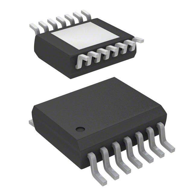
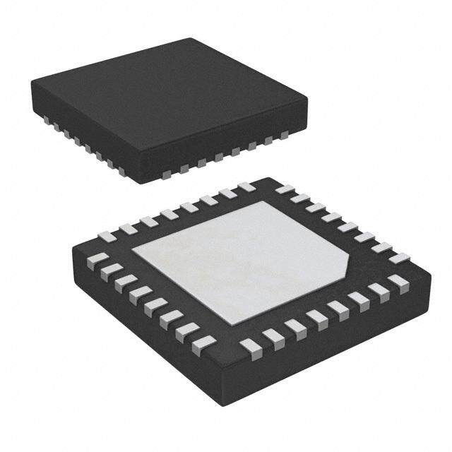
| 描述 | IC LED DRIVER TRIAC DIMM 14SOICLED照明驱动器 Triac Dimmable Offline LED Driver 14-SOIC |
| 产品分类 | |
| 品牌 | Texas Instruments |
| 产品手册 | |
| 产品图片 |
|
| rohs | 符合RoHS无铅 / 符合限制有害物质指令(RoHS)规范要求 |
| 产品系列 | LED照明电子器件,LED照明驱动器,Texas Instruments LM3445M/NOPBPowerWise® |
| 数据手册 | |
| 产品型号 | LM3445M/NOPB |
| 产品目录页面 | |
| 产品种类 | LED照明驱动器 |
| 供应商器件封装 | 14-SOICN |
| 其它名称 | LM3445M |
| 内部驱动器 | 无 |
| 包装 | 管件 |
| 参考设计库 | http://designs.digikey.com/library/4294959899/4294959898/444http://designs.digikey.com/library/4294959899/4294959898/308http://designs.digikey.com/library/4294959899/4294959898/479http://designs.digikey.com/library/4294959899/4294959898/772http://designs.digikey.com/library/4294959899/4294959898/511 |
| 商标 | Texas Instruments |
| 安装类型 | 表面贴装 |
| 安装风格 | SMD/SMT |
| 宽度 | 3.91 mm |
| 封装 | Tube |
| 封装/外壳 | 14-SOIC(0.154",3.90mm 宽) |
| 封装/箱体 | SOIC-14 |
| 工作温度 | -40°C ~ 125°C |
| 工作频率 | 30 kHz to 1 MHz |
| 工厂包装数量 | 55 |
| 恒压 | - |
| 恒流 | 是 |
| 拓扑 | PWM,降压(降压) |
| 拓扑结构 | Buck |
| 最大工作温度 | + 125 C |
| 最大电源电流 | 2850 uA |
| 最小工作温度 | - 40 C |
| 标准包装 | 55 |
| 特色产品 | http://www.digikey.com/cn/zh/ph/ns/lm3445.html |
| 电压-电源 | 8 V ~ 12 V |
| 电压-输出 | - |
| 类型 | Inductive |
| 类型-初级 | - |
| 类型-次级 | 高亮度 LED(HBLED) |
| 系列 | LM3445 |
| 设计资源 | http://www.digikey.com/product-highlights/cn/zh/texas-instruments-webench-design-center/3176 |
| 输入电压 | 8 V to 12 V |
| 输出数 | 1 |
| 输出电流 | 1 A |
| 输出端数量 | 1 Output |
| 输出类型 | Constant Current |
| 频率 | 30kHz ~ 1MHz |


- 商务部:美国ITC正式对集成电路等产品启动337调查
- 曝三星4nm工艺存在良率问题 高通将骁龙8 Gen1或转产台积电
- 太阳诱电将投资9.5亿元在常州建新厂生产MLCC 预计2023年完工
- 英特尔发布欧洲新工厂建设计划 深化IDM 2.0 战略
- 台积电先进制程称霸业界 有大客户加持明年业绩稳了
- 达到5530亿美元!SIA预计今年全球半导体销售额将创下新高
- 英特尔拟将自动驾驶子公司Mobileye上市 估值或超500亿美元
- 三星加码芯片和SET,合并消费电子和移动部门,撤换高东真等 CEO
- 三星电子宣布重大人事变动 还合并消费电子和移动部门
- 海关总署:前11个月进口集成电路产品价值2.52万亿元 增长14.8%


PDF Datasheet 数据手册内容提取
Product Sample & Technical Tools & Support & Reference Folder Buy Documents Software Community Design LM3445 SNVS570M–JANUARY2009–REVISEDNOVEMBER2015 LM3445 TRIAC Dimmable Offline LED Driver 1 Features 3 Description • TRIACDimDecoderCircuitforLEDDimming The LM3445 is an adaptive constant off-time AC/DC 1 buck(step-down)constantcurrentcontrollerdesigned • ApplicationVoltageRange80V to277V AC AC to be compatible with TRIAC dimmers. The LM3445 • CapableofControllingLEDCurrentsGreater provides a constant current for illuminating high Than1A power LEDs and includes a TRIAC dim decoder. The • AdjustableSwitchingFrequency dim decoder allows wide range LED dimming using standard TRIAC dimmers. The high frequency • LowQuiescentCurrent capable architecture allows the use of small external • AdaptiveProgrammableOff-TimeAllowsfor passive components. The LM3445 includes a bleeder ConstantRippleCurrent circuit to ensure proper TRIAC operation by allowing • ThermalShutdown current flow while the line voltage is low to enable proper firing of the TRIAC. A passive PFC circuit • No120-HzFlicker ensuresgoodpowerfactorbydrawingcurrentdirectly • LowProfile10-PinVSSOPPackageor14-Pin from the line for most of the cycle, and provides a SOIC constant positive voltage to the buck regulator. • PatentedDriveArchitecture Additional features include thermal shutdown, current limitandV under-voltagelockout. CC 2 Applications DeviceInformation(1) • RetroFitTRIACDimming PARTNUMBER PACKAGE BODYSIZE(NOM) • SolidStateLighting VSSOP(10) 3.00mm×3.00mm • IndustrialandCommercialLighting LM3445 SOIC(14) 3.91mm×8.65mm • ResidentialLighting (1) For all available packages, see the orderable addendum at theendofthedatasheet. TypicalLM3445LEDDriverApplicationCircuit EfficiencyvsLineVoltage V+ D3 VBUCK 95.0 C7 + D9 14 Series connected LEDs BR1 C10 R2 D4 D8 C9 + C12 VL-ED R4 90.0 DTIMRMIAECR Q1 D2 VLED- %) VAC D1 R5 D10 CY ( 85.0 C5 Q3 N E CI L2 FFI 10 Series connected LEDs LM3445MM E 80.0 1 ASNS U1 BLDR10 R1 ICOLL 2 FLTR1 VCC9 75.0 80 90 100 110 120 130 140 C3 3 DIM GATE8 Q2 LINE VOLTAGE (VAC) 4COFF ISNS7 5FLTR2 GND6 R3 C4 C11 1 An IMPORTANT NOTICE at the end of this data sheet addresses availability, warranty, changes, use in safety-critical applications, intellectualpropertymattersandotherimportantdisclaimers.PRODUCTIONDATA.
LM3445 SNVS570M–JANUARY2009–REVISEDNOVEMBER2015 www.ti.com Table of Contents 1 Features.................................................................. 1 7.3 FeatureDescription...................................................8 2 Applications........................................................... 1 7.4 DeviceFunctionalModes........................................20 3 Description............................................................. 1 8 ApplicationandImplementation........................ 21 4 RevisionHistory..................................................... 2 8.1 ApplicationInformation............................................21 8.2 TypicalApplication .................................................29 5 PinConfigurationandFunctions......................... 3 9 PowerSupplyRecommendations...................... 33 6 Specifications......................................................... 4 10 Layout................................................................... 33 6.1 AbsoluteMaximumRatings .....................................4 6.2 ESDRatings..............................................................4 10.1 LayoutGuidelines.................................................33 6.3 RecommendedOperatingConditions.......................4 10.2 LayoutExample....................................................33 6.4 ThermalInformation..................................................4 11 DeviceandDocumentationSupport................. 34 6.5 ElectricalCharacteristics...........................................5 11.1 CommunityResources..........................................34 6.6 TypicalCharacteristics..............................................6 11.2 Trademarks...........................................................34 7 DetailedDescription.............................................. 8 11.3 ElectrostaticDischargeCaution............................34 7.1 Overview...................................................................8 11.4 Glossary................................................................34 7.2 FunctionalBlockDiagram.........................................8 12 Mechanical,Packaging,andOrderable Information........................................................... 34 4 Revision History NOTE:Pagenumbersforpreviousrevisionsmaydifferfrompagenumbersinthecurrentversion. ChangesfromRevisionL(May2013)toRevisionM Page • AddedESDRatingstable,FeatureDescriptionsection,DeviceFunctionalModes,ApplicationandImplementation section,PowerSupplyRecommendationssection,Layoutsection,DeviceandDocumentationSupportsection,and Mechanical,Packaging,andOrderableInformationsection.................................................................................................. 1 • Removedmaximumleadtemperature(soldering). ............................................................................................................... 4 ChangesfromRevisionK(May2013)toRevisionL Page • ChangedlayoutofNationalDataSheettoTIformat........................................................................................................... 32 2 SubmitDocumentationFeedback Copyright©2009–2015,TexasInstrumentsIncorporated ProductFolderLinks:LM3445
LM3445 www.ti.com SNVS570M–JANUARY2009–REVISEDNOVEMBER2015 5 Pin Configuration and Functions DGSPackage 10-PinVSSOP DPackage TopView 14-PinSOIC TopView ASNS 1 10 BLDR COFF 1 14 DIM FLTR1 2 9 VCC N/C 2 13 FLTR1 DIM 3 8 GATE FLTR2 3 12 ASNS COFF 4 7 ISNS GND 4 11 N/C FLTR2 5 6 GND N/C 5 10 BLDR N/C 6 9 VCC ISNS 7 8 GATE PinFunctions PIN I/O DESCRIPTION NAME SOIC VSSOP PWMoutputoftheTRIACdimdecodercircuit.Outputsa0to4-VPWMsignal ASNS 12 1 O withadutycycleproportionaltotheTRIACdimmeron-time. Bleederpin.Providestheinputsignaltotheangledetectcircuitryaswellasa BLDR 10 10 I currentpaththroughaswitched230-Ωresistortoensureproperfiringofthe TRIACdimmer. OFFtimesettingpin.Ausersetcurrentandcapacitorconnectedfromthe COFF 1 4 I outputtothispinsetstheconstantOFFtimeoftheswitchingcontroller. Input/outputdualfunctiondimpin.ThispincanbedrivenwithanexternalPWM signaltodimtheLEDs.Itmayalsobeusedasanoutputsignalandconnected DIM 14 3 I/O totheDIMpinofotherLM3445sorotherLEDdriverstodimmultipleLED circuitssimultaneously. Firstfilterinput.The120-HzPWMsignalfromASNSisfilteredtoaDCsignal andcomparedtoa1to3V,5.85-kHzramptogenerateahigherfrequency FLTR1 13 2 I PWMsignalwithadutycycleproportionaltotheTRIACdimmerfiringangle. Pullabove4.9-V(typical)totri-stateDIM. Secondfilterinput.AcapacitortiedtothispinfiltersthePWMdimmingsignal FLTR2 3 5 I tosupplyaDCvoltagetocontroltheLEDcurrent.Couldalsobeusedasan analogdimminginput. PowerMOSFETdriverpin.Thisoutputprovidesthegatedriveforthepower GATE 8 8 O switchingMOSFETofthebuckcontroller. GND 4 6 — Circuitgroundconnection LEDcurrentsensepin.ConnectaresistorfrommainswitchingMOSFET ISNS 7 7 I source,ISNStoGNDtosetthemaximumLEDcurrent. N/C 2,5,6,11 — — NoConnect Inputvoltagepin.Thispinprovidesthepowerfortheinternalcontrolcircuitry VCC 9 9 O andgatedriver. Copyright©2009–2015,TexasInstrumentsIncorporated SubmitDocumentationFeedback 3 ProductFolderLinks:LM3445
LM3445 SNVS570M–JANUARY2009–REVISEDNOVEMBER2015 www.ti.com 6 Specifications 6.1 Absolute Maximum Ratings See(1) (2)(3) MIN MAX UNIT BLDRtoGND –0.3 17 V V ,GATE,FLTR1toGND –0.3 14 V CC ISNStoGND –0.3 2.5 V ASNS,DIM,FLTR2,COFFtoGND –0.3 7 V COFFInputCurrent 100 mA ContinuousPowerDissipation(4) InternallyLimited JunctionTemperature(T ) 150 °C J-MAX StorageTemperature –65 150 °C (1) StressesbeyondthoselistedunderAbsoluteMaximumRatingsmaycausepermanentdamagetothedevice.Thesearestressratings only,whichdonotimplyfunctionaloperationofthedeviceattheseoranyotherconditionsbeyondthoseindicatedunderRecommended OperatingConditions.Exposuretoabsolute-maximum-ratedconditionsforextendedperiodsmayaffectdevicereliability (2) IfMilitary/Aerospacespecifieddevicesarerequired,pleasecontacttheTexasInstrumentsSalesOffice/Distributorsforavailabilityand specifications. (3) AllvoltagesarewithrespecttothepotentialattheGNDpin,unlessotherwisespecified. (4) Internalthermalshutdowncircuitryprotectsthedevicefrompermanentdamage.ThermalshutdownengagesatT =165°C(typ.)and J disengagesat+T =145°C(typ). J 6.2 ESD Ratings VALUE UNIT Human-bodymodel(HBM),perANSI/ESDA/JEDECJS-001(1)(2) ±2000 V(ESD) Electrostaticdischarge Charged-devicemodel(CDM),perJEDECspecificationJESD22- V C101(3) ±1000 (1) JEDECdocumentJEP155statesthat500-VHBMallowssafemanufacturingwithastandardESDcontrolprocess. (2) HumanBodyModel,applicablestd.JESD22-A114-C. (3) JEDECdocumentJEP157statesthat250-VCDMallowssafemanufacturingwithastandardESDcontrolprocess. 6.3 Recommended Operating Conditions MIN MAX UNIT V 8 12 V CC JunctionTemperature –40 125 °C 6.4 Thermal Information LM3445 THERMALMETRIC(1) DGS(VSSOP) D(SOIC) UNIT 10PINS 14PINS R Junction-to-ambientthermalresistance 159 82.8 °C/W θJA R Junction-to-case(top)thermalresistance 54.5 40.2 °C/W θJC(top) R Junction-to-boardthermalresistance 78.7 37.5 °C/W θJB ψ Junction-to-topcharacterizationparameter 5.3 6.4 °C/W JT ψ Junction-to-boardcharacterizationparameter 77.5 37.2 °C/W JB R Junction-to-case(bottom)thermalresistance N/A N/A °C/W θJC(bot) (1) Formoreinformationabouttraditionalandnewthermalmetrics,seetheSemiconductorandICPackageThermalMetricsapplication report,SPRA953. 4 SubmitDocumentationFeedback Copyright©2009–2015,TexasInstrumentsIncorporated ProductFolderLinks:LM3445
LM3445 www.ti.com SNVS570M–JANUARY2009–REVISEDNOVEMBER2015 6.5 Electrical Characteristics AllTypicallimitsareforT =25°CandallMaximumandMinimumlimitsapplyoverthefullOperatingTemperatureRange(T J J =−40°Cto+125°C).MinimumandMaximumlimitsarespecifiedthroughtest,design,orstatisticalcorrelation.Typicalvalues representthemostlikelyparametricnormatT =+25ºC,andareprovidedforreferencepurposesonly. J PARAMETER TESTCONDITIONS MIN TYP MAX UNIT BLEEDER R BleederresistancetoGND I =10mA 230 325 Ω BLDR BLDR V SUPPLY CC I Operatingsupplycurrent 2 2.85 mA VCC Risingthreshold 7.4 7.7 V Fallingthreshold 6 6.4 V CC-UVLO Hysterisis 1 COFF V Timeoutthreshold 1.225 1.276 1.327 V COFF R Offtimersinkingimpedance 33 60 Ω COFF t Restarttimer 180 µs COFF CURRENTLIMIT V ISNSlimitthreshold 1.174 1.269 1.364 V ISNS Leadingedgeblankingtime 125 ns Currentlimitresetdelay 180 µs t ISNS ISNS=0to1.75-V ISNSlimittoGATEdelay 33 ns step INTERNALPWMRAMP f Frequency 5.85 kHz RAMP Valleyvoltage 0.96 1 1.04 V V RAMP Peakvoltage 2.85 3 3.08 D Maximumdutycycle 96.5% 98% RAMP DIMDECODER t Angledetectrisingthreshold ObservedonBLDRpin 6.79 7.21 7.81 V ANG_DET ASNSfilterdelay 4 µs V ASNS ASNSVMAX 3.85 4 4.15 V ASNSdrivecapabilitysink V =2V 7.6 ASNS ASNSdrivecapabilitysource V =2V –4.3 ASNS I mA ASNS DIMlowsinkcurrent V =1V 1.65 2.8 DIM DIMHighsourcecurrent V =4V –4 –3 DIM PWMinputvoltage DIMlowvoltage 0.9 1.33 V threshold V DIM DIMhighvoltage 2.33 3.15 V Tri-statethresholdvoltage ApplytoFLTR1pin 4.87 5.25 V TSTH R DIMcomparatortri-stateimpedance 10 MΩ DIM CURRENTSENSECOMPARATOR V FLTR2opencircuitvoltage 720 750 780 mV FLTR2 R FLTR2impedance 420 kΩ FLTR2 V Currentsensecomparatoroffsetvoltage –4 0.1 4 mV OS GATEDRIVEOUTPUT V GATEhighsaturation I =50mA 0.24 0.5 DRVH GATE V V GATElowsaturation I =100mA 0.22 0.5 DRVL GATE Peaksoucecurrent GATE=V /2 –0.77 CC I A DRV Peaksinkcurrent GATE=V /2 0.88 CC Copyright©2009–2015,TexasInstrumentsIncorporated SubmitDocumentationFeedback 5 ProductFolderLinks:LM3445
LM3445 SNVS570M–JANUARY2009–REVISEDNOVEMBER2015 www.ti.com Electrical Characteristics (continued) AllTypicallimitsareforT =25°CandallMaximumandMinimumlimitsapplyoverthefullOperatingTemperatureRange(T J J =−40°Cto+125°C).MinimumandMaximumlimitsarespecifiedthroughtest,design,orstatisticalcorrelation.Typicalvalues representthemostlikelyparametricnormatT =+25ºC,andareprovidedforreferencepurposesonly. J PARAMETER TESTCONDITIONS MIN TYP MAX UNIT Risetime C =1nF 15 load t ns DV Falltime C =1nF 15 load THERMALSHUTDOWN Thermalshutdowntemperature 165 T See (1) °C SD Thermalshutdownhysteresis 20 (1) Junction-to-ambientthermalresistanceishighlyapplicationandboard-layoutdependent.Inapplicationswherehighmaximumpower dissipationexists,specialcaremustbepaidtothermaldissipationissuesinboarddesign.Inapplicationswherehighpowerdissipation and/orpoorpackagethermalresistanceispresent,themaximumambienttemperaturemayhavetobederated.Maximumambient temperature(T )isdependentonthemaximumoperatingjunctiontemperature(T =125°C),themaximumpowerdissipation A-MAX J-MAX-OP ofthedeviceintheapplication(P ),andthejunction-toambientthermalresistanceofthepart/packageintheapplication(R ),as D-MAX θJA givenbythefollowingequation:T =T –(R ×P ). A-MAX J-MAX-OP θJA D-MAX 6.6 Typical Characteristics 300k 95.0 14 Series connected LEDs 250k 7 LEDs in Series (VO = 24.5V) 90.0 200k %) Hz) Y ( (W 150k NC 85.0 S E f CI 100k FI F 10 Series connected LEDs E 80.0 50k C11 = 2.2 nF, R3 = 348 k: 0 75.0 80 90 100 110 120 130 140 80 90 100 110 120 130 140 LINE VOLTAGE (VAC) LINE VOLTAGE (VAC) Figure1.f vsInputLineVoltage Figure2.EfficiencyvsInputLineVoltage SW 300 8.0 UVLO (VCC) Rising 280 7.5 (cid:214)) SISTOR ( 260 VLO(V) 7.0 E 240 U UVLO (VCC) Falling R R D L 6.5 B 220 200 6.0 -50 -25 0 25 50 75 100 125 150 -50 -25 0 25 50 75 100 125 150 TEMPERATURE (°C) TEMPERATURE (°C) Figure3.BLDRResistorvsTemperature Figure4.V UVLOvsTemperature CC 6 SubmitDocumentationFeedback Copyright©2009–2015,TexasInstrumentsIncorporated ProductFolderLinks:LM3445
LM3445 www.ti.com SNVS570M–JANUARY2009–REVISEDNOVEMBER2015 Typical Characteristics (continued) 200.0 1.29 190.0 1.28 s) 180.0 (nMIN (V)FF 1.27 N- 170.0 VO O OFF Threshold at C11 t 1.26 160.0 150.0 1.25 -50 -25 0 25 50 75 100 125 150 -50 -25 0 25 50 75 100 125 150 TEMPERATURE (°C) TEMPERATURE (°C) Figure5.MinOn-Time(t )vsTemperature Figure6.OffThreshold(C11)vsTemperature ON 1.50 15.0 Series 100 units tested connected LEDs Room (25°C) 1.25 Hot (125°C) Q W FRE 1.00 3 LEDs UNITS 10.0 Cold (-40°C) D S OF ZE 5 LEDs R ORMALI 0.75 7 LEDs NUMBE 5.0 N 0.50 9 LEDs 0.25 0.0 0 50 100 150 200 80 100 120 140 160 180 VBUCK (V) LEADING EDGE BLANKING (ns) Figure7.NormalizedVariationinf overV Voltage Figure8.LeadingEdgeBlankingVariationOver SW BUCK Temperature Copyright©2009–2015,TexasInstrumentsIncorporated SubmitDocumentationFeedback 7 ProductFolderLinks:LM3445
LM3445 SNVS570M–JANUARY2009–REVISEDNOVEMBER2015 www.ti.com 7 Detailed Description 7.1 Overview The LM3445 contains all the necessary circuitry to build a line-powered (mains powered) constant current LED driverwhoseoutputcurrentcanbecontrolledwithaconventionalTRIACdimmer. 7.2 Functional Block Diagram VCC BLDR ANGLE DETECT INTERNAL LM3445 REGULATORS 4 Ps 7.2V 230 VCC UVLO BLEEDER THERMAL MOSFET COFF SHUTDOWN DRIVER COFF GATE 33: 1.276V S Q START ASNS R 0V to 4V LATCH 750 mV DIM DECODER 50k 4.9V Tri-State 370k PWM FLTR1 CONTROLLER RAMP I-LIM 3V RA5M.9P k GHEzN. 1V 1.27V 1k ISNS DIM LEADING EDGE BLANKING FLTR2 125 ns GND 7.3 Feature Description 7.3.1 OverviewofPhaseControlDimming AbasicphasecontrolledTRIACdimmercircuitisshowninFigure9. BRIGHT R1 (cid:27) 250 k(cid:214) DIM TRIAC MAINS AC R2 (cid:27) 3.3 k(cid:214) DIAC C1 (cid:27) 100 nF LOAD Figure9. BasicTRIACDimmer 8 SubmitDocumentationFeedback Copyright©2009–2015,TexasInstrumentsIncorporated ProductFolderLinks:LM3445
LM3445 www.ti.com SNVS570M–JANUARY2009–REVISEDNOVEMBER2015 Feature Description (continued) An RC network consisting of R1, R2, and C1 delay the turn on of the TRIAC until the voltage on C1 reaches the triggervoltageofthediac.Increasingtheresistanceofthepotentiometer(wipermovingdownward)increasesthe turn-on delay which decreases the on-time or conduction angle of the TRIAC (θ). This reduces the average power delivered to the load. Voltage waveforms for a simple TRIAC dimmer are shown in Figure 10. Figure 10a shows the full sinusoid of the input voltage. Even when set to full brightness, few dimmers will provide 100% on- time,i.e.,thefullsinusoid. (a) (b) DELAY ? (c) ? DELAY Figure10. LineVoltageandDimmingWaveforms Figure 10b shows a theoretical waveform from a dimmer. The on-time is often referred to as the conduction angle and may be stated in degrees or radians. The off-time represents the delay caused by the RC circuit feedingtheTRIAC.Theoff-timebereferredtoasthefiringangleandissimply180° -θ. Figure 10c shows a waveform from a so-called reverse phase dimmer, sometimes referred to as an electronic dimmer. These typically are more expensive, microcontroller based dimmers that use switching elements other than TRIACs. Note that the conduction starts from the zero-crossing, and terminates some time later. This methodofcontrolreducesthenoisespikeatthetransition. Since the LM3445 has been designed to assess the relative on-time and control the LED current accordingly, mostphase-controldimmers,bothforwardandreversephase,maybeusedwithsuccess. Copyright©2009–2015,TexasInstrumentsIncorporated SubmitDocumentationFeedback 9 ProductFolderLinks:LM3445
LM3445 SNVS570M–JANUARY2009–REVISEDNOVEMBER2015 www.ti.com Feature Description (continued) 7.3.2 TheoryofOperation RefertoFigure11whichshowstheLM3445alongwithbasicexternalcircuitry. V+ D3 VBUCK + C7 D9 BR1 C10 D8 V + LED R2 D4 C9 C12 - R4 TRIAC Q1 V DIMMER D2 LED- VAC D1 R5 D10 C5 Q3 L2 LM3445MM 1 ASNS BLDR10 U1 R1 I COLL 2 FLTR1 VCC 9 C3 3 DIM 8 Q2 GATE 4 COFF ISNS 7 R3 5 FLTR2 GND 6 C4 C11 Figure11. LM3445Schematic 10 SubmitDocumentationFeedback Copyright©2009–2015,TexasInstrumentsIncorporated ProductFolderLinks:LM3445
LM3445 www.ti.com SNVS570M–JANUARY2009–REVISEDNOVEMBER2015 Feature Description (continued) 7.3.3 SensingtheRectifiedTRIACWaveform A bridge rectifier, BR1, converts the line (mains) voltage (Figure 12c) into a series of half-sines as shown in Figure12b.Figure12ashowsatypicalvoltagewaveformafterdiodeD3(valleyfillcircuit,orV ). BUCK VBUCK (a) VBR1 (b) VAC (c) t Figure12. VoltageWaveformsAfterBridgeRectifierWithoutTRIACDimming Figure 13c and Figure 13b show typical TRIAC dimmed voltage waveforms before and after the bridge rectifier. Figure13ashowsatypicalTRIACdimmedvoltagewaveformafterdiodeD3(valleyfillcircuit,orV ). BUCK V BUCK (a) t V BR1 (b) t V AC (c) t delay ? Figure13. VoltageWaveformsAfterBridgeRectifierWithTRIACDimming Copyright©2009–2015,TexasInstrumentsIncorporated SubmitDocumentationFeedback 11 ProductFolderLinks:LM3445
LM3445 SNVS570M–JANUARY2009–REVISEDNOVEMBER2015 www.ti.com Feature Description (continued) 7.3.4 LM3445LineSensingCircuitry An external series pass regulator (R2, D1, and Q1) translates the rectified line voltage to a level where it can be sensedbytheBLDRpinontheLM3445. V+ R2 Q1 D2 D1 R5 C5 R11 LM3445MM U1 1 ASNS BLDR 10 R1 2 FLTR1 VCC 9 C3 3 DIM GATE 8 4 COFF ISNS 7 5 FLTR2 GND 6 C4 Figure14. LM3445ACLineSenseCircuitry D1 is typically a 15-V Zener diode which forces transistor Q1 to stand-off most of the rectified line voltage. Having no capacitance on the source of Q1 allows the voltage on the BLDR pin to rise and fall with the rectified linevoltageasthelinevoltagedropsbelowzenervoltageD1(seeAngleDetect). A diode-capacitor network (D2, C5) is used to maintain the voltage on the VCC pin while the voltage on the BLDRpingoeslow.ThisprovidesthesupplyvoltagetooperatetheLM3445. Resistor R5 is used to bleed charge out of any stray capacitance on the BLDR node and may be used to provide thenecessaryholdingcurrentforthedimmerwhenoperatingatlightoutputcurrents. 7.3.5 TRIACHoldingCurrentResistor In order to emulate an incandescent light bulb (essentially a resistor) with any LED driver, the existing TRIAC will require a small amount of holding current throughout the AC line cycle. An external resistor (R5) needs to be placed on the source of Q1 to GND to perform this function. Most existing TRIAC dimmers only require a few milliamps of current to hold them on. A few less expensive TRIACs sold on the market will require a bit more current.ThevalueofresistorR5willdependon: • WhattypeofTRIACtheLM3445willbeusedwith • HowmanylightfixturesarerunningoffoftheTRIAC 12 SubmitDocumentationFeedback Copyright©2009–2015,TexasInstrumentsIncorporated ProductFolderLinks:LM3445
LM3445 www.ti.com SNVS570M–JANUARY2009–REVISEDNOVEMBER2015 Feature Description (continued) With a single LM3445 circuit on a common TRIAC dimmer, a holding current resistor between 3 kΩ and 5 kΩ will be required. As the number of LM3445 circuits is added to a single dimmer, the holding resistor R5’s resistance can be increased. A few TRIAC dimmers will require a resistor as low as 1 kΩ or lower for a single LM3445 circuit. The trade-off will be performance vs efficiency. As the holding resistor R5 is increased, the overall efficiencyperLM3445willalsoincrease. 7.3.6 AngleDetect The Angle Detect circuit uses a comparator with a fixed threshold voltage of 7.21 V to monitor the BLDR pin to determinewhethertheTRIACisonoroff.TheoutputofthecomparatordrivestheASNSbufferandalsocontrols theBleedercircuit.A4µsdelaylineontheoutputisusedtofilteroutnoisethatcouldbepresentonthissignal. The output of the Angle Detect circuit is limited to a 0 V to 4 V swing by the buffer and presented to the ASNS pin.R1andC3comprisealow-passfilterwithabandwidthontheorderof1Hz. TheAngleDetectcircuitanditsfilterproduceaDClevelwhichcorrespondstothedutycycle(relativeon-time)of theTRIACdimmer.Asaresult,theLM3445willworkequallywellwith50-Hzor60-Hzlinevoltages. 7.3.7 Bleeder While the BLDR pin is below the 7.21-V threshold, the bleeder MOSFET is on to place a small load (230 Ω) on the series pass regulator. This additional load is necessary to complete the circuit through the TRIAC dimmer so that the dimmer delay circuit can operate correctly. Above 7.21 V, the bleeder resistor is removed to increase efficiency. 7.3.8 FLTR1Pin The FLTR1 pin has two functions. Normally, it is fed by ASNS through filter components R1 and C3 and drives the dim decoder. However, if the FLTR1 pin is tied above 4.9 V (typical), for example, to VCC, the Ramp Comparatoristri-stated,disablingthedimdecoder.SeeMaster/SlaveOperation 7.3.9 DimDecoder The ramp generator produces a 5.85-kHz saw tooth wave with a minimum of 1 V and a maximum of 3 V. The filteredASNSsignalenterspinFLTR1whereitiscomparedagainsttheoutputoftheRampGenerator. The output of the ramp comparator will have an on-time which is inversely proportional to the average voltage level at pin FLTR1. However, since the FLTR1 signal can vary between 0 V and 4 V (the limits of the ASNS pin), and the Ramp Generator signal only varies between 1 V and 3 V, the output of the ramp comparator will be on continuously for V < 1 V and off continuously for V > 3 V. This allows a decoding range from 45° to FLTR1 FLTR1 135° toprovidea0to100%dimmingrange. The output of the ramp comparator drives both a common-source N-channel MOSFET through a Schmitt trigger and the DIM pin (see Master/Slave Operation for further functions of the DIM pin). The MOSFET drain is pulled upto750mVbya50-kΩresistor. Since the MOSFET inverts the output of the ramp comparator, the drain voltage of the MOSFET is proportional to the duty cycle of the line voltage that comes through the TRIAC dimmer. The amplitude of the ramp generator causesthisproportionalityto"hardlimit"fordutycyclesabove75%andbelow25%. The MOSFET drain signal next passes through an RC filter comprised of an internal 370-kΩ resistor, and an external capacitor on pin FLTR2. This forms a second low pass filter to further reduce the ripple in this signal, whichisusedasareferencebythePWMcomparator.ThisRCfilterisgenerallysetto10Hz. The net effect is that the output of the dim decoder is a DC voltage whose amplitude varies from near 0 V to 750 mV as the duty cycle of the dimmer varies from 25% to 75%. This corresponds to conduction angles of 45° to 135°,respectively. The output voltage of the Dim Decoder directly controls the peak current that will be delivered by Q2 during its on-time.SeeBuckConverter fordetails. AstheTRIACfiresbeyond135°,theDIMdecodernolongercontrolsthedimming.AtthispointtheLEDswilldim graduallyforoneoftworeasons: 1. The voltage at V decreases and the buck converter runs out of headroom and causes LED current to BUCK Copyright©2009–2015,TexasInstrumentsIncorporated SubmitDocumentationFeedback 13 ProductFolderLinks:LM3445
LM3445 SNVS570M–JANUARY2009–REVISEDNOVEMBER2015 www.ti.com Feature Description (continued) decreaseasV decreases. BUCK 2. Minimumon-timeisreachedwhichfixestheduty-cycleandthereforereducesthevoltageatV . BUCK The transition from dimming with the DIM decoder to headroom or minimum on-time dimming is seamless. LED currentsfromfullloadtoaslowas0.5mAcanbeeasilyachieved. 7.3.10 Valley-FillCircuit V supplies the power which drives the LED string. Diode D3 allows V to remain high while V+ cycles on BUCK BUCK and off. V has a relatively small hold capacitor C10 which reduces the voltage ripple when the valley fill BUCK capacitors are being charged. However, the network of diodes and capacitors shown between D3 and C10 make up a valley-fill circuit. The valley-fill circuit can be configured with two or three stages. The most common configurationistwostages.Figure15illustratesatwoandthreestagevalley-fillcircuit. V+ D3 VBUCK V+ D3 VBUCK C7 + D9 R6 C7 + D9 R6 D6 C10 D8 R8 + C10 D8 R8 D4 + R7 D5 C8 C9 D4 D7 C9 + R7 Figure15. TwoandThreeStageValleyFillCircuit The valley-fill circuit allows the buck regulator to draw power throughout a larger portion of the AC line. This allows the capacitance needed at V to be lower than if there were no valley-fill circuit, and adds passive BUCK power factor correction (PFC) to the application. Besides better power factor correction, a valley-fill circuit allows thebuckconvertertooperatewhileseparatecircuitrytranslatesthedimminginformation.Thisallowsfordimming thatisn’tsubjectto120Hzflickerthatcanbeperceivedbythehumaneye. 7.3.11 Valley-FillOperation When the input line is high, power is derived directly through D3. The term input line is high can be explained as follows. The valley-fill circuit charges capacitors C7 and C9 in series (see Figure 16) when the input line is high. 14 SubmitDocumentationFeedback Copyright©2009–2015,TexasInstrumentsIncorporated ProductFolderLinks:LM3445
LM3445 www.ti.com SNVS570M–JANUARY2009–REVISEDNOVEMBER2015 Feature Description (continued) V BUCK V+ D3 + + C7 V BUCK 2 - C10 + D8 D4 VBUCK + C9 2 - Figure16. TwoStageValley-FillCircuitWhenACLineisHigh Thepeakvoltageofatwostagevalley-fillcapacitoris: V 2 V = AC-RMS VF-CAP 2 (1) As the AC line decreases from its peak value every cycle, there will be a point where the voltage magnitude of the AC line is equal to the voltage that each capacitor is charged. At this point diode D3 becomes reversed biased, and the capacitors are placed in parallel to each other (Figure 17), and V equals the capacitor BUCK voltage. V BUCK V+ D3 + + C7 V BUCK D9 - C10 D8 + D4 + V BUCK C9 - Figure17. TwoStageValley-FillCircuitWhenACLineisLow Copyright©2009–2015,TexasInstrumentsIncorporated SubmitDocumentationFeedback 15 ProductFolderLinks:LM3445
LM3445 SNVS570M–JANUARY2009–REVISEDNOVEMBER2015 www.ti.com Feature Description (continued) A three stage valley-fill circuit performs exactly the same as two-stage valley-fill circuit except now three capacitorsarenowchargedinseries,andwhenthelinevoltagedecreasesto: V 2 V = AC-RMS VF-CAP 3 (2) DiodeD3isreversedbiasedandthreecapacitorsareinparalleltoeachother. The valley-fill circuit can be optimized for power factor, voltage hold up and overall application size and cost. The LM3445 will operate with a single stage or a three stage valley-fill circuit as well. Resistor R8 functions as a current limiting resistor during start-up, and during the transition from series to parallel connection. Resistors R6 andR7are1-MΩ bleederresistors,andmayormaynotbenecessaryforeachapplication. 7.3.12 BuckConverter The LM3445 is a buck controller that uses a proprietary constant off-time method to maintain constant current through a string of LEDs. While transistor Q2 is on, current ramps up through the inductor and LED string. A resistor R3 senses this current and this voltage is compared to the reference voltage at FLTR2. When this sensed voltage is equal to the reference voltage, transistor Q2 is turned off and diode D10 conducts the current through the inductor and LEDs. Capacitor C12 eliminates most of the ripple current seen in the inductor. Resistor R4, capacitor C11, and transistor Q3 provide a linear current ramp that sets the constant off-time for a given outputvoltage. VBUCK R4 C12 D10 Q3 L2 I LM3445MM COLL 8 Q2 GATE 4 COFF ISNS 7 R3 GND 6 C11 Figure18. LM3445BuckRegulationCircuit 16 SubmitDocumentationFeedback Copyright©2009–2015,TexasInstrumentsIncorporated ProductFolderLinks:LM3445
LM3445 www.ti.com SNVS570M–JANUARY2009–REVISEDNOVEMBER2015 Feature Description (continued) 7.3.13 OverviewofConstantOff-TimeControl Abuckconverter’sconversionratioisdefinedusingEquation3. V t O = D = ON = t x f V t + t ON SW IN ON OFF (3) Constant off-time control architecture operates by simply defining the off-time and allowing the on-time, and therefore the switching frequency, to vary as either V or V changes. The output voltage is equal to the LED IN O string voltage (V ), and should not change significantly for a given application. The input voltage or V in LED BUCK this analysis will vary as the input line varies. The length of the on-time is determined by the sensed inductor current through a resistor to a voltage reference at a comparator. During the on-time, denoted by t , MOSFET ON switch Q2 is on causing the inductor current to increase. During the on-time, current flows from V , through BUCK theLEDs,throughL2,Q2,andfinallythroughR3toground.Atsomepointintime,theinductorcurrentreachesa maximum (I ) determined by the voltage sensed at R3 and the ISNS pin. This sensed voltage across R3 is L2-PK comparedagainstthevoltageofdimdecoderoutput,FLTR2,atwhichpointQ2isturnedoffbythecontroller. I L2-PK ’i L I AVE I L2-MIN I (t) L2 t t t ON OFF Figure19. InductorCurrentWaveforminCCM Duringtheoff-perioddenotedbyt ,thecurrentthroughL2continuestoflowthroughtheLEDsviaD10. OFF 7.3.14 Master/SlaveOperation Multiple LM3445s can be configured so that large strings of LEDs can be controlled by a single TRIAC dimmer. Bydoingso,smoothconsistentdimmingformultipleLEDcircuitsisachieved. When the FLTR1 pin is tied above 4.9 V (typical), preferably to VCC, the ramp comparator is tri-stated, disabling the dim decoder. This allows one or more LM3445 devices or PWM LED driver devices (slaves) to be controlled byasingleLM3445(master)byconnectingtheirDIMpinstogether. 7.3.15 Master/SlaveConfiguration TI offers an LM3445 demonstration PCB for customer evaluation through our website. The following description andtheoryusesreferencedesignatorsthatfollowourevaluationPCB.TheLM3445Master/Slaveschematicsare illustrated below (Figure 20 through Figure 22) for clarity. Each board contains a separate circuit for the Master and Slave function. Both the Master and Slave boards will need to be modified from their original stand alone function so that they can be coupled together. Only the Master LM3445 requires use of the Master/Slave circuit foranynumberofslaves. 7.3.16 MasterBoardModifications • RemoveR10andreplacewithaBAS40diode • ConnectTP18toTP14(V ) CC • ConnectTP17(gateofQ5)toTP15(gateofQ2) 7.3.17 SlaveBoardModifications • RemoveR11(disconnectsBLDR) Copyright©2009–2015,TexasInstrumentsIncorporated SubmitDocumentationFeedback 17 ProductFolderLinks:LM3445
LM3445 SNVS570M–JANUARY2009–REVISEDNOVEMBER2015 www.ti.com Feature Description (continued) • TieTP14(FLTR1)toV CC 7.3.18 Master/SlaveInterconnection • ConnectTP19ofMastertoTP10ofSlave(MasterVCCControl) • ConnectTP6(DIMpin)ofMastertoTP6(DIMpin)ofSlave(MasterDIMControl) 7.3.19 Master/SlaveTheoryofOperation By placing two series diodes on the Master VCC circuit one forces the master VCC UVLO to become the dominant threshold. When Master VCC drops below UVLO, GATE stops switching and the RC timer (>200 µs) risesabovetheTL431threshold(2.5V)whichinturnpullsdownonthegateoftheSlavepassdevice(Q1). The valley-fill circuit could consist of one large circuit to power all LM3445 series connected, or each LM3445 circuitcouldhaveaseparatevalley-fillcircuitlocatednearthebuckconverter. 7.3.20 Master/SlaveConnectionDiagram V+ V+ MASTER LM3445 SLAVE LM3445 R2 R2 TP10 Q1 Q1 MASTER D2 R10 D2 BAS40 VCC CTRL D1 D1 R5 C5 R5 C5 R11 R11 LM3445MM LM3445MM R1 U1 MASTER-VBUCK U1 1 ASNS BLDR 10 1 ASNS BLDR 10 2 FLTR1 VCC 9 2 FLTR1 VCC 9 C3 MASTER- 3 DIM GATE 8 3 DIM GATE 8 BUCK 4 COFF ISNS 7 4 COFF ISNS 7 SLAVE BUCK 5 FLTR2 GND 6 TP18 TP19 5 FLTR2 GND 6 C4 C4 R13 SLAVE-VBUCK C13 R12 D11 TP17 Q5 C14 MASTER/ MASTER SLAVE DIM CTRL CIRCUIT Figure20. MasterSlaveConfiguration 18 SubmitDocumentationFeedback Copyright©2009–2015,TexasInstrumentsIncorporated ProductFolderLinks:LM3445
LM3445 www.ti.com SNVS570M–JANUARY2009–REVISEDNOVEMBER2015 Feature Description (continued) 7.3.21 Master/SlaveBlockDiagrams V+ N BR1 Valley-Fill Valley-Fill Valley-Fill CKT CKT CKT MASTER L BUCK SLAVE SLAVE BUCK BUCK MASTER CTRL MASTER MASTER VCC DIM Figure21. Master/SlaveConfigurationWithSeparateValley-FillCircuits Copyright©2009–2015,TexasInstrumentsIncorporated SubmitDocumentationFeedback 19 ProductFolderLinks:LM3445
LM3445 SNVS570M–JANUARY2009–REVISEDNOVEMBER2015 www.ti.com Feature Description (continued) V+ Large Valley-Fill CKT N BR1 MASTER L BUCK SLAVE SLAVE BUCK BUCK MASTER CTRL MASTER MASTER VCC CTRL DIM CTRL Figure22. Master/SlaveConfigurationWithOneValley-FillCircuit 7.3.22 ThermalShutdown Thermal shutdown limits total power dissipation by turning off the output switch when the IC junction temperature exceeds 165°C. After thermal shutdown occurs, the output switch doesn’t turn on until the junction temperature dropstoapproximately145°C. 7.4 Device Functional Modes Thisdevicedoesnothaveanyadditionalfunctionalmodes. 20 SubmitDocumentationFeedback Copyright©2009–2015,TexasInstrumentsIncorporated ProductFolderLinks:LM3445
LM3445 www.ti.com SNVS570M–JANUARY2009–REVISEDNOVEMBER2015 8 Application and Implementation NOTE Information in the following applications sections is not part of the TI component specification, and TI does not warrant its accuracy or completeness. TI’s customers are responsible for determining suitability of components for their purposes. Customers should validateandtesttheirdesignimplementationtoconfirmsystemfunctionality. 8.1 Application Information 8.1.1 DeterminingDuty-Cycle(D) AsshowninEquation4,dutycycle(D)approximatelyequals: V t LED ON = D = = t x f V t + t ON SW BUCK ON OFF (4) Withefficiencyconsidered: V 1 LED u = D K V BUCK (5) Forsimplicity,chooseefficiencybetween75%and85%. 8.1.2 CalculatingOff-Time The Off-Time of the LM3445 is set by the user and remains fairly constant as long as the voltage of the LED stack remains constant. Calculating the off-time is the first step in determining the switching frequency of the converter,whichisintegralindeterminingsomeexternalcomponentvalues. PNP transistor Q3, resistor R4, and the LED string voltage define a charging current into capacitor C11. A constantcurrentintoacapacitorcreatesalinearchargingcharacteristic,asshowninEquation6. dv i = C dt (6) Resistor R4, capacitor C11 and the current through resistor R4 (i ), which is approximately equal to V /R4, COLL LED areallfixed.Therefore,dvisfixedandlinear,anddt(t )cannowbecalculated. OFF R4 t = C11 x 1.276V x OFF V LED (7) Equation8showscommonequationsfordeterminingdutycycleandswitchingfrequencyinanybuckconverter. 1 f = SW t + t OFF ON t V D = ON = LED t + t V ON OFF BUCK t ’¶(cid:3)= OFF t + t ON OFF (8) Therefore: D 1 - D f = , and f = SW t SW t ON OFF (9) Withefficiencyofthebuckconverterinmind,asshowninEquation10. V LED = K u D V BUCK (10) Substituteequationsandrearrange: Copyright©2009–2015,TexasInstrumentsIncorporated SubmitDocumentationFeedback 21 ProductFolderLinks:LM3445
LM3445 SNVS570M–JANUARY2009–REVISEDNOVEMBER2015 www.ti.com Application Information (continued) § 1 VLED • ¤1 (cid:16) u ‚ K V ' BUCK „ f = SW t OFF (11) Off-time,andswitchingfrequencycannowbecalculatedusingtheequationsabove. 8.1.3 SettingtheSwitchingFrequency Selecting the switching frequency for nominal operating conditions is based on tradeoffs between efficiency (betteratlowfrequency)andsolutionsizeandcost(smallerathighfrequency). The input voltage to the buck converter (V ) changes with both line variations and over the course of each BUCK half-cycle of the input line voltage. The voltage across the LED string will, however, remain constant, and thereforetheoff-timeremainsconstant. The on-time, and therefore the switching frequency, will vary as the V voltage changes with line voltage. A BUCK good design practice is to choose a desired nominal switching frequency knowing that the switching frequency willdecreaseasthelinevoltagedropsandincreaseasthelinevoltageincreases(seeFigure23). 1.50 Series connected LEDs 1.25 Q E R F W 1.00 3 LEDs S D E 5 LEDs Z LI 0.75 A M R O 7 LEDs N 0.50 9 LEDs 0.25 0 50 100 150 200 VBUCK (V) Figure23. GraphicalIllustrationofSwitchingFrequencyvsV BUCK The off-time of the LM3445 can be programmed for switching frequencies ranging from 30 kHz to over 1 MHz. A trade-offbetweenefficiencyandsolutionsizemustbeconsideredwhendesigningtheLM3445application. Themaximumswitchingfrequencyattainableislimitedonlybytheminimumon-timerequirement(200ns). Worst case scenario for minimum on time is when V is at its maximum voltage (AC high line) and the LED BUCK stringvoltage(V )isatitsminimumvalue. LED V 1 LED(MIN) 1 t = u ON(MIN) K V f (cid:3) BUCK(MAX) SW (12) ThemaximumvoltageseenbytheBuckConverteris: V = V x 2 BUCK(MAX) AC-RMS(MAX) (13) 22 SubmitDocumentationFeedback Copyright©2009–2015,TexasInstrumentsIncorporated ProductFolderLinks:LM3445
LM3445 www.ti.com SNVS570M–JANUARY2009–REVISEDNOVEMBER2015 Application Information (continued) 8.1.4 InductorSelection The controlled off-time architecture of the LM3445 regulates the average current through the inductor (L2), and therefore the LED string current. The input voltage to the buck converter (V ) changes with line variations and BUCK over the course of each half-cycle of the input line voltage. The voltage across the LED string is relatively constant, and therefore the current through R4 is constant. This current sets the off-time of the converter and therefore the output volt-second product (V x off-time) remains constant. A constant volt-second product LED makesitpossibletokeeptheripplethroughtheinductorconstantasthevoltageatV varies. BUCK VBUCK VLED C12 - D10 L2 VL2 - Q2 R3 Figure24. LM3445ExternalComponentsoftheBuckConverter TheequationforanidealinductorisshowninEquation14. di Q = L dt (14) Given a fixed inductor value, L, this equation states that the change in the inductor current over time is proportionaltothevoltageappliedacrosstheinductor. Duringtheon-time,thevoltageappliedacrosstheinductoris, V =V –(V +V +I ×R3) (15) L(ON-TIME) BUCK LED DS(Q2) L2 Since the voltage across the MOSFET switch (Q2) is relatively small, as is the voltage across sense resistor R3, wecansimplifythistoapproximately, V =V –V (16) L(ON-TIME) BUCK LED Duringtheoff-time,thevoltageseenbytheinductorisapproximately: V =V (17) L(OFF-TIME) LED The value of V will be relatively constant, because the LED stack voltage will remain constant. If we L(OFF-TIME) rewrite the equation for an inductor inserting what we know about the circuit during the off-time, we get Equation18. ’i VL(OFF-TIME) = VLED = L x ’t (I - I ) V = V = L x (MAX) (MIN) L(OFF-TIME) LED ’t (18) Re-arrangingthisgivesusEquation19. Copyright©2009–2015,TexasInstrumentsIncorporated SubmitDocumentationFeedback 23 ProductFolderLinks:LM3445
LM3445 SNVS570M–JANUARY2009–REVISEDNOVEMBER2015 www.ti.com Application Information (continued) V ’i # t x LED OFF L2 (19) From this we can see that the ripple current (Δi) is proportional to off-time (t ) multiplied by a voltage which is OFF dominatedbyV dividedbyaconstant(L2). LED TheseequationscanberearrangedtocalculatethedesiredvalueforinductorL2. V L2 #(cid:3) tOFF x ’LEiD (20) Where: t = 1 (cid:16) 1 u VLED OFF K V (cid:3) BUCK f SW (21) Finally: V 1 (cid:16) 1u VLED LED K V (cid:3) BUCK L2 = f x ’i SW (22) SeeTypicalApplicationtobetterunderstandthedesignprocess. 8.1.5 SettingtheLEDCurrent The LM3445 constant off-time control loop regulates the peak inductor current (I ). The average inductor current L2 equals the average LED current (I ). Therefore the average LED current is regulated by regulating the peak AVE inductorcurrent. I L2-PK ’i L I AVE I L2-MIN I (t) L2 t t t ON OFF Figure25. InductorCurrentWaveforminCCM Knowing the desired average LED current, I and the nominal inductor current ripple, Δi , the peak current for AVE L anapplicationrunningincontinuousconductionmode(CCM)isdefinedinEquation23. ’i I = I + L L2-PK AVE 2 (23) Or,themaximum,orundimmed,LEDcurrentwouldthenbe, ’i I = I - L AVE(UNDIM) L2-PK(UNDIM) 2 (24) This is important to calculate because this peak current multiplied by the sense resistor R3 will determine when the internal comparator is tripped. The internal comparator turns the control MOSFET off once the peak sensed voltagereaches750mV,asshowninEquation25. 750 mV I = L-PK(UNDIM) R3 (25) 24 SubmitDocumentationFeedback Copyright©2009–2015,TexasInstrumentsIncorporated ProductFolderLinks:LM3445
LM3445 www.ti.com SNVS570M–JANUARY2009–REVISEDNOVEMBER2015 Application Information (continued) Current Limit: Under normal circumstances, the trip voltage on the PWM comparator would be less than or equal to 750 mV, depending on the amount of dimming. However, if there is a short circuit or an excessive load on the output, higher than normal switch currents will cause a voltage above 1.27 V on the ISNS pin which will trip the I-LIM comparator. The I-LIM comparator will reset the RS latch, turning off Q2. It will also inhibit the Start Pulse Generator and the COFF comparator by holding the COFF pin low. A delay circuit will prevent the start of anothercyclefor180µs. 8.1.6 ValleyFillCapacitors Determiningvoltageratingandcapacitancevalueofthevalley-fillcapacitors: Equation26showsthemaximumvoltageseenbythevalley-fillcapacitorsis: V 2 AC(MAX) V = VF-CAP #stages (26) This is, of course, if the capacitors chosen have identical capacitance values and split the line voltage equally. Often a 20% difference in capacitance could be observed between like capacitors. Therefore a voltage rating marginof25%to50%shouldbeconsidered. 8.1.6.1 DeterminingtheCapacitanceValueoftheValley-FillCapacitors The valley fill capacitors should be sized to supply energy to the buck converter (V ) when the input line is BUCK less than its peak divided by the number of stages used in the valley fill (t ). The capacitance value should be X calculated when the TRIAC is not firing, that is, when full LED current is being drawn by the LED string. The maximumpowerisdeliveredtotheLEDstringatthistime,andthereforethemostcapacitanceisrequired. 30° 150° t V X BUCK t 8.33 ms 0° 180° Figure26. TwoStageValley-FillV VoltageWithNoTRIACDimming BUCK From the above illustration and the equation for current in a capacitor, i = C × dV/dt, the amount of capacitance neededatV iscalculatedasfollows: BUCK At60Hz,andavalley-fillcircuitoftwostages,theholduptime(t )requiredatV iscalculatedasfollows.The X BUCK totalangleofanAChalfcycleis180° andthetotaltimeofahalfAClinecycleis8.33ms.Whentheangleofthe AC waveform is at 30° and 150°, the voltage of the AC line is exactly ½ of its peak. With a two stage valley-fill circuit, this is the point where the LED string switches from power being derived from AC line to power being derived from the hold up capacitors (C7 and C9). 60° out of 180° of the cycle or 1/3 of the cycle the power is derived from the hold up capacitors (1/3 × 8.33 ms = 2.78 ms). This is equal to the hold up time (dt) from the above equation, and dv is the amount of voltage the circuit is allowed to droop. From the next section (“Determining Maximum Number of Series Connected LEDs Allowed”) we know the minimum V voltage will BUCK be about 45 V for a 90 V to 135 V line. At 90 V low line operating condition input, ½ of the peak voltage is AC AC AC 64 V. Therefore, with some margin the voltage at V can not droop more than about 15 V (dv). (i) is equal to BUCK (P /V ), where P is equal to (V × I ). Total capacitance (C7 in parallel with C9) can now be OUT BUCK OUT LED LED calculated.SeeTypicalApplicationforfurthercalculationsofthevalley-fillcapacitors. Copyright©2009–2015,TexasInstrumentsIncorporated SubmitDocumentationFeedback 25 ProductFolderLinks:LM3445
LM3445 SNVS570M–JANUARY2009–REVISEDNOVEMBER2015 www.ti.com Application Information (continued) 8.1.6.2 DeterminingMaximumNumberofSeriesConnectedLEDsAllowed The LM3445 is an off-line buck topology LED driver. A buck converter topology requires that the input voltage (V ) of the output circuit must be greater than the voltage of the LED stack (V ) for proper regulation. One BUCK LED must determine what the minimum voltage observed by the buck converter will be before the maximum number ofLEDsallowedcanbedetermined.Twovariableswillhavetobedeterminedinordertoaccomplishthis. 1. AC line operating voltage. This is usually 90 V to 135 V for North America. Although the LM3445 can AC AC operateatmuchlowerandhigherinputvoltagesarangeisneededtoillustratethedesignprocess. 2. Howmanystagesareimplementedinthevalley-fillcircuit(1,2or3). Inthisexamplethemostcommonvalley-fillcircuitwillbeused(twostages). 45° 90° 135° VPEAK V AC t Figure27. ACLinewithFiringAngles Figure 28 shows three TRIAC dimmed waveforms. One can easily see that the peak voltage (V ) from 0° to PEAK 90° willalwaysbe: VAC-RMS-PK 2 (27) OncetheTRIACisfiringatananglegreaterthan90° thepeakvoltagewilllowerandequaltoEquation28. VAC-RMS-PK 2 x SIN(T) (28) ThevoltageatV withavalleyfillstageoftwowilllooksimilartothewaveformsofFigure29. BUCK The purpose of the valley fill circuit is to allow the buck converter to pull power directly off of the AC line when the line voltage is greater than its peak voltage divided by two (two stage valley fill circuit). During this time, the capacitors within the valley fill circuit (C7 and C8) are charged up to the peak of the AC line voltage. Once the line drops below its peak divided by two, the two capacitors are placed in parallel and deliver power to the buck converter.OnecannowseethatifthepeakoftheAClinevoltageisloweredduetovariationsinthelinevoltage, or if the TRIAC is firing at an angle above 90°, the DC offset (V ) will lower. V is the lowest value that voltage DC DC V willencounter. BUCK VAC-RMS(MIN) 2x SIN(T) V = BUCK(MIN) #stages (29) Example: Linevoltage=90V to135V AC AC Valley-Fill=twostage 90 2 x SIN(135o) V = = 45V BUCK(MIN) 2 (30) 26 SubmitDocumentationFeedback Copyright©2009–2015,TexasInstrumentsIncorporated ProductFolderLinks:LM3445
LM3445 www.ti.com SNVS570M–JANUARY2009–REVISEDNOVEMBER2015 Application Information (continued) Dependingonwhattypeandvalueofcapacitorsareused,somederatingshouldbeusedforvoltagedroopwhen the capacitors are delivering power to the buck converter. When the TRIAC is firing at 135° the current through the LED string will be small. Therefore the droop should be small at this point and a 5% voltage droop should be a sufficient derating. With this derating, the lowest voltage the buck converter will see is about 42.5 V in this example. VPEAK VPEAK V PEAK V V+ V+ + t t t θ= 45° θ= 90° θ= 135° Figure28. ACLineWithVariousFiringAngles V PEAK V PEAK V V + + VVDDCC VDC t t Figure29. V WaveformsWithVariousFiringAngles BUCK To determine how many LEDs can be driven, take the minimum voltage the buck converter will see (42.5 V) and divideitbytheworstcaseforwardvoltagedropofasingleLED. Example:42.5V/3.7V=11.5LEDs(11LEDswithmargin) 8.1.7 OutputCapacitor A capacitor placed in parallel with the LED or array of LEDs can be used to reduce the LED current ripple while keeping the same average current through both the inductor and the LED array. With a buck topology the output inductance (L2) can now be lowered, making the magnetics smaller and less expensive. With a well designed converter, you can assume that all of the ripple will be seen by the capacitor, and not the LEDs. One must ensure that the capacitor you choose can handle the RMS current of the inductor. See manufacture’s data sheets to ensure compliance. Usually an X5R or X7R capacitor between 1 µF and 10 µF of the proper voltage ratingwillbesufficient. 8.1.8 SwitchingMOSFET The main switching MOSFET should be chosen with efficiency and robustness in mind. The maximum voltage acrosstheswitchingMOSFETwillequal: VDS(MAX) = VAC-RMS(MAX) 2 (31) Theaveragecurrentratingshouldbegreaterthan: I =I (D ) (32) DS-MAX LED(-AVE) MAX Copyright©2009–2015,TexasInstrumentsIncorporated SubmitDocumentationFeedback 27 ProductFolderLinks:LM3445
LM3445 SNVS570M–JANUARY2009–REVISEDNOVEMBER2015 www.ti.com Application Information (continued) 8.1.9 Re-CirculatingDiode The LM3445 Buck converter requires a re-circulating diode D10 (see the Typical Application circuit to carry the inductor current during the MOSFET Q2 off-time. The most efficient choice for D10 is a diode with a low forward drop and near-zero reverse recovery time that can withstand a reverse voltage of the maximum voltage seen at V .Foracommon110V ±20%line,thereversevoltagecouldbeashighas190V. BUCK AC V t(cid:3)V 2 D AC-RMS(MAX) (33) Thecurrentratingmustbeatleast: I =(1-DMIN)×Iledave (34) D Or: V LED(MIN) ID = 1 - V x ILED(AVE) BUCK(MAX) (35) 28 SubmitDocumentationFeedback Copyright©2009–2015,TexasInstrumentsIncorporated ProductFolderLinks:LM3445
LM3445 www.ti.com SNVS570M–JANUARY2009–REVISEDNOVEMBER2015 8.2 Typical Application TP3 V+ VBUCK D3 TP4 BR1 LED+ +C7 D9 R6 D8 R8 C10 C2 L4 D4 +C9 R7 VLED R4 C12 C15 L3 D10 TP5 C1 TP10 V+ LED- VLED- D12 Q3 R2 L5 Q1 TP14 D2 R10 L2 D1 R5 C5 L1 R11 I RT1 COLL R14 TP11 LM3445MM F1 U1 1 ASNS BLDR 10 J1 R1 2 FLTR1 VCC 9 TP12 VAC C3 TP15 TRIAC 3 DIM GATE 8 Q2 DIMMER TP6 TP16 4 COFF ISNS 7 Master-Slave Circuitry R3 5 FLTR2 GND 6 TP18 TP19 C4 C13 R12 R13 TP7-9 C11 D11 TP17 Q5 C14 Figure30. LM3445DesignExample1Input=90V to135V ,V =7 ×HBLEDStringApplicationat AC AC LED 400MA Copyright©2009–2015,TexasInstrumentsIncorporated SubmitDocumentationFeedback 29 ProductFolderLinks:LM3445
LM3445 SNVS570M–JANUARY2009–REVISEDNOVEMBER2015 www.ti.com Typical Application (continued) 8.2.1 DesignRequirements Known: 1. Inputvoltagerange(90V –135V ) AC AC 2. NumberofLEDsinseries=7 3. ForwardvoltagedropofasingleLED=3.6V 4. LEDstackvoltage=(7× 3.6V)=25.2V Choose: 1. Nominalswitchingfrequency,f =350kHz SW-TARGET 2. I =400mA LED(AVE) 3. Δi(usually15%-30%of )=(0.30 ×400mA)=120mA ILED(AVE) 4. Valleyfillstages(1,2,or3)=2 5. Assumedminimumefficiency=80% 8.2.2 DetailedDesignProcedure Thefollowingdesignexampleillustratestheprocessofcalculatingexternalcomponentvalues. Calculate: 1. CalculateminimumvoltageV equals: BUCK 90 2 x SIN(135o) V = = 45V BUCK(MIN) 2 (36) 2. CalculatemaximumvoltageV equals: BUCK VBUCK(MAX) = 135 2 = 190V (37) 3. Calculatet atV nominallinevoltage: OFF BUCK 1 25.2V 1 (cid:16) u 0.8 115 2 t = = 3.23 Ps OFF (250 kHz) (38) 4. Calculatet athighlinetoensurethatt >200ns: ON(MIN) ON(MIN) 1 25.2V u 0.8 135 2 t = u 3.23 Ps = 638 ns ON (MIN) 1 25.2V 1 (cid:16) u 0.8 135 2 (39) 5. CalculateC11andR4: 6. ChoosecurrentthroughR4:(between50 µAand100µA)70µA V LED R4 = = 360 k: I COLL (40) 7. Useastandardvalueof365kΩ 8. CalculateC11: V t LED OFF C11 = = 175 pF R4 1.276 (41) 9. Usestandardvalueof120pF 10. Calculateripplecurrent:400mA ×0.30=120mA 11. Calculateinductorvalueatt =3 µs: OFF 1 25.2V 25.2V 1 (cid:16) u 0.8 115 2 L2= = 580 PH (350 kHz x 0.1A) (42) 12. ChooseC10:1µF200V 30 SubmitDocumentationFeedback Copyright©2009–2015,TexasInstrumentsIncorporated ProductFolderLinks:LM3445
LM3445 www.ti.com SNVS570M–JANUARY2009–REVISEDNOVEMBER2015 Typical Application (continued) 13. Calculate valley-fill capacitor values: V low line = 90 V , V minimum equals 60 V (no TRIAC AC AC BUCK dimmingatmaximumLEDcurrent).Setdroopfor20Vmaximumatfullloadandlowline. dv i = C dt where • iequalsP /V (270mA). OUT BUCK • dVequals20V. • dtequals2.77ms. • C equals37µF. TOTAL ThereforeC7=C9=22 µF. (43) Table1.BillofMaterials QTY REFDES DESCRIPTION MANUFACTURER MANUFACTURERPN 1 U1 IC,CTRLR,DRVR-LED,VSSOP10 TI LM3445MM 1 BR1 BridgeRectifiier,SMT,400V,800mA DiodesInc HD04-T 1 L1 CommonmodefilterDIP4NS,900mA,700µH Panasonic ELF-11090E 1 L2 Inductor,SHLD,SMT,1A,470µH Coilcraft MSS1260-474-KLB 2 L3,L4 Diffmodeinductor,500mA1mH Coilcraft MSS1260-105KL-KLB 1 L5 BeadInductor,160Ω,6A Steward HI1206T161R-10 3 C1,C2,C15 Cap,Film,X2Y2,12.5MM,250V ,20%,10 Panasonic ECQ-U2A103ML AC nF 1 C3 Cap,X7R,0603,16V,10%,470nF MuRata GRM188R71C474KA88D 1 C4 Cap,X7R,0603,16V,10%,100nF MuRata GRM188R71C104KA01D 2 C5,C6 Cap,X5R,1210,25V,10%,22µF MuRata GRM32ER61E226KE15L 2 C7,C9 Cap,AL,200V,105C,20%,33µF UCC EKXG201ELL330MK20S 1 C10 Cap,Film,250V,5%,10nF Epcos B32521C3103J 1 C12 Cap,X7R,1206,50V,10%,1.0uF Kemet C1206F105K5RACTU 1 C11 Cap,C0G,0603,100V,5%,120pF MuRata GRM1885C2A121JA01D 1 C13 Cap,X7R,0603,50V,10%,1.0nF Kemet C0603C102K5RACTU 1 C14 Cap,X7R,0603,50V,10%,22nF Kemet C0603C223K5RACTU 1 D1 Diode,ZNR,SOT23,15V,5% OnSemi BZX84C15LT1G 2 D2,D13 Diode,SCH,SOD123,40V,120mA NXP BAS40H 4 D3,D4,D8,D9 Diode,FR,SOD123,200V,1A Rohm RF071M2S 1 D10 Diode,FR,SMB,400V,1A OnSemi MURS140T3G 1 D11 IC,SHNT,ADJ,SOT23,2.5V,0.5% TI TL431BIDBZR 1 D12 TVS,VBR=209V LittleFuse P6SMB220CA 1 R1 Resistor,0603,1%,280kΩ Panasonic ERJ-3EKF2803V 1 R2 Resistor,1206,1%,100kΩ Panasonic ERJ-8ENF1003V 1 R3 Resistor,1210,5%,1.8Ω Panasonic ERJ-14RQJ1R8U 1 R4 Resistor,0603,1%,576kΩ Panasonic ERJ-3EKF5763V 1 R5 Resistor,1206,1%,1.00kΩ Panasonic ERJ-8ENF1001V 2 R6,R7 Resistor,0805,1%,1.00MΩ Rohm MCR10EZHF1004 2 R8,R10 Resistor,1206,0.0Ω Yageo RC1206JR-070RL 1 R9 Resistor,1812,0.0Ω 1 R11 Resistor,0603,0.0Ω Yageo RC0603JR-070RL 1 R12 Resistor,0603,1%,33.2kΩ Panasonic ERJ-3EKF3322V 1 R13 Resistor,0603,1%,2.0kΩ Panasonic ERJ-3EKF2001V 1 R14 Resistor,0805,1%,3.3MΩ Rohm MCR10EZHF3304 1 RT1 Thermistor,120V,1.1A,50Ωat25°C Thermometrics CL-140 Copyright©2009–2015,TexasInstrumentsIncorporated SubmitDocumentationFeedback 31 ProductFolderLinks:LM3445
LM3445 SNVS570M–JANUARY2009–REVISEDNOVEMBER2015 www.ti.com Typical Application (continued) Table1.BillofMaterials(continued) QTY REFDES DESCRIPTION MANUFACTURER MANUFACTURERPN 2 Q1,Q2 XSTR,NFET,DPAK,300V,4A Fairchild FQD7N30TF 1 Q3 XSTR,PNP,SOT23,300V,500mA Fairchild MMBTA92 1 Q5 XSTR,NFET,SOT23,100V,170mA Fairchild BSS123 1 J1 TerminalBlock2pos PhoenixContact 1715721 1 F1 Fuse,125V,1,25A bel SSQ1.25 8.2.3 ApplicationCurve 95.0 14 Series connected LEDs 90.0 %) CY ( 85.0 N E CI FFI 10 Series connected LEDs E 80.0 75.0 80 90 100 110 120 130 140 LINE VOLTAGE (VAC) Figure31. EfficiencyversusInputVoltage 32 SubmitDocumentationFeedback Copyright©2009–2015,TexasInstrumentsIncorporated ProductFolderLinks:LM3445
LM3445 www.ti.com SNVS570M–JANUARY2009–REVISEDNOVEMBER2015 9 Power Supply Recommendations UseanyACpowersupplycapableofthemaximumapplicationrequirementsforvoltageandtotalpower. 10 Layout 10.1 Layout Guidelines Keep the low power components for ASNS, FLTR1, FLTR2, and COFF close to the LM3445 with short traces. The ISNS trace should also be as short and direct as possible. Keep the high current switching paths generated byR3,Q2,L2,andD10asshortaspossibletominimizegeneratedswitchingnoiseandimproveEMI. 10.2 Layout Example RECTIFIED AC INPUT LED+ = VIA ASNS BLDR FLTR1 VCC LED- DIM GATE COFF ISNS FLTR2 GND GND Figure32. LayoutRecommendation Copyright©2009–2015,TexasInstrumentsIncorporated SubmitDocumentationFeedback 33 ProductFolderLinks:LM3445
LM3445 SNVS570M–JANUARY2009–REVISEDNOVEMBER2015 www.ti.com 11 Device and Documentation Support 11.1 Community Resources The following links connect to TI community resources. Linked contents are provided "AS IS" by the respective contributors. They do not constitute TI specifications and do not necessarily reflect TI's views; see TI's Terms of Use. TIE2E™OnlineCommunity TI'sEngineer-to-Engineer(E2E)Community.Createdtofostercollaboration amongengineers.Ate2e.ti.com,youcanaskquestions,shareknowledge,exploreideasandhelp solveproblemswithfellowengineers. DesignSupport TI'sDesignSupport QuicklyfindhelpfulE2Eforumsalongwithdesignsupporttoolsand contactinformationfortechnicalsupport. 11.2 Trademarks E2EisatrademarkofTexasInstruments. Allothertrademarksarethepropertyoftheirrespectiveowners. 11.3 Electrostatic Discharge Caution Thesedeviceshavelimitedbuilt-inESDprotection.Theleadsshouldbeshortedtogetherorthedeviceplacedinconductivefoam duringstorageorhandlingtopreventelectrostaticdamagetotheMOSgates. 11.4 Glossary SLYZ022—TIGlossary. Thisglossarylistsandexplainsterms,acronyms,anddefinitions. 12 Mechanical, Packaging, and Orderable Information The following pages include mechanical, packaging, and orderable information. This information is the most current data available for the designated devices. This data is subject to change without notice and revision of thisdocument.Forbrowser-basedversionsofthisdatasheet,refertotheleft-handnavigation. 34 SubmitDocumentationFeedback Copyright©2009–2015,TexasInstrumentsIncorporated ProductFolderLinks:LM3445
PACKAGE OPTION ADDENDUM www.ti.com 6-Feb-2020 PACKAGING INFORMATION Orderable Device Status Package Type Package Pins Package Eco Plan Lead/Ball Finish MSL Peak Temp Op Temp (°C) Device Marking Samples (1) Drawing Qty (2) (6) (3) (4/5) LM3445M/NOPB ACTIVE SOIC D 14 55 Green (RoHS SN Level-1-260C-UNLIM LM3445M & no Sb/Br) LM3445MM/NOPB ACTIVE VSSOP DGS 10 1000 Green (RoHS NIPDAUAG | SN Level-1-260C-UNLIM -40 to 125 SULB & no Sb/Br) LM3445MMX/NOPB ACTIVE VSSOP DGS 10 3500 Green (RoHS NIPDAUAG | SN Level-1-260C-UNLIM -40 to 125 SULB & no Sb/Br) LM3445MX/NOPB ACTIVE SOIC D 14 2500 Green (RoHS SN Level-1-260C-UNLIM LM3445M & no Sb/Br) (1) The marketing status values are defined as follows: ACTIVE: Product device recommended for new designs. LIFEBUY: TI has announced that the device will be discontinued, and a lifetime-buy period is in effect. NRND: Not recommended for new designs. Device is in production to support existing customers, but TI does not recommend using this part in a new design. PREVIEW: Device has been announced but is not in production. Samples may or may not be available. OBSOLETE: TI has discontinued the production of the device. (2) RoHS: TI defines "RoHS" to mean semiconductor products that are compliant with the current EU RoHS requirements for all 10 RoHS substances, including the requirement that RoHS substance do not exceed 0.1% by weight in homogeneous materials. Where designed to be soldered at high temperatures, "RoHS" products are suitable for use in specified lead-free processes. TI may reference these types of products as "Pb-Free". RoHS Exempt: TI defines "RoHS Exempt" to mean products that contain lead but are compliant with EU RoHS pursuant to a specific EU RoHS exemption. Green: TI defines "Green" to mean the content of Chlorine (Cl) and Bromine (Br) based flame retardants meet JS709B low halogen requirements of <=1000ppm threshold. Antimony trioxide based flame retardants must also meet the <=1000ppm threshold requirement. (3) MSL, Peak Temp. - The Moisture Sensitivity Level rating according to the JEDEC industry standard classifications, and peak solder temperature. (4) There may be additional marking, which relates to the logo, the lot trace code information, or the environmental category on the device. (5) Multiple Device Markings will be inside parentheses. Only one Device Marking contained in parentheses and separated by a "~" will appear on a device. If a line is indented then it is a continuation of the previous line and the two combined represent the entire Device Marking for that device. (6) Lead/Ball Finish - Orderable Devices may have multiple material finish options. Finish options are separated by a vertical ruled line. Lead/Ball Finish values may wrap to two lines if the finish value exceeds the maximum column width. Important Information and Disclaimer:The information provided on this page represents TI's knowledge and belief as of the date that it is provided. TI bases its knowledge and belief on information provided by third parties, and makes no representation or warranty as to the accuracy of such information. Efforts are underway to better integrate information from third parties. TI has taken and Addendum-Page 1
PACKAGE OPTION ADDENDUM www.ti.com 6-Feb-2020 continues to take reasonable steps to provide representative and accurate information but may not have conducted destructive testing or chemical analysis on incoming materials and chemicals. TI and TI suppliers consider certain information to be proprietary, and thus CAS numbers and other limited information may not be available for release. In no event shall TI's liability arising out of such information exceed the total purchase price of the TI part(s) at issue in this document sold by TI to Customer on an annual basis. Addendum-Page 2
PACKAGE MATERIALS INFORMATION www.ti.com 22-Sep-2017 TAPE AND REEL INFORMATION *Alldimensionsarenominal Device Package Package Pins SPQ Reel Reel A0 B0 K0 P1 W Pin1 Type Drawing Diameter Width (mm) (mm) (mm) (mm) (mm) Quadrant (mm) W1(mm) LM3445MM/NOPB VSSOP DGS 10 1000 178.0 12.4 5.3 3.4 1.4 8.0 12.0 Q1 LM3445MMX/NOPB VSSOP DGS 10 3500 330.0 12.4 5.3 3.4 1.4 8.0 12.0 Q1 LM3445MX/NOPB SOIC D 14 2500 330.0 16.4 6.5 9.35 2.3 8.0 16.0 Q1 PackMaterials-Page1
PACKAGE MATERIALS INFORMATION www.ti.com 22-Sep-2017 *Alldimensionsarenominal Device PackageType PackageDrawing Pins SPQ Length(mm) Width(mm) Height(mm) LM3445MM/NOPB VSSOP DGS 10 1000 210.0 185.0 35.0 LM3445MMX/NOPB VSSOP DGS 10 3500 367.0 367.0 35.0 LM3445MX/NOPB SOIC D 14 2500 367.0 367.0 35.0 PackMaterials-Page2
PACKAGE OUTLINE DGS0010A VSSOP - 1.1 mm max height SCALE 3.200 SMALL OUTLINE PACKAGE C 5.05 4.75 TYP SEATING PLANE A PIN 1 ID 0.1 C AREA 8X 0.5 10 1 3.1 2X 2.9 NOTE 3 2 5 6 0.27 10X 0.17 B 3.1 0.1 C A B 1.1 MAX 2.9 NOTE 4 0.23 TYP SEE DETAIL A 0.13 0.25 GAGE PLANE 0.15 0.7 0 - 8 0.05 0.4 DETAIL A TYPICAL 4221984/A 05/2015 NOTES: 1. All linear dimensions are in millimeters. Any dimensions in parenthesis are for reference only. Dimensioning and tolerancing per ASME Y14.5M. 2. This drawing is subject to change without notice. 3. This dimension does not include mold flash, protrusions, or gate burrs. Mold flash, protrusions, or gate burrs shall not exceed 0.15 mm per side. 4. This dimension does not include interlead flash. Interlead flash shall not exceed 0.25 mm per side. 5. Reference JEDEC registration MO-187, variation BA. www.ti.com
EXAMPLE BOARD LAYOUT DGS0010A VSSOP - 1.1 mm max height SMALL OUTLINE PACKAGE 10X (1.45) 10X (0.3) SYMM (R0.05) TYP 1 10 SYMM 8X (0.5) 5 6 (4.4) LAND PATTERN EXAMPLE SCALE:10X SOOPLEDNEINRG MASK METAL MSOELTDAEL RU NMDAESRK SOOPLEDNEINRG MASK 0.05 MAX 0.05 MIN ALL AROUND ALL AROUND NON SOLDER MASK SOLDER MASK DEFINED DEFINED SOLDER MASK DETAILS NOT TO SCALE 4221984/A 05/2015 NOTES: (continued) 6. Publication IPC-7351 may have alternate designs. 7. Solder mask tolerances between and around signal pads can vary based on board fabrication site. www.ti.com
EXAMPLE STENCIL DESIGN DGS0010A VSSOP - 1.1 mm max height SMALL OUTLINE PACKAGE 10X (1.45) SYMM (R0.05) TYP 10X (0.3) 1 10 SYMM 8X (0.5) 5 6 (4.4) SOLDER PASTE EXAMPLE BASED ON 0.125 mm THICK STENCIL SCALE:10X 4221984/A 05/2015 NOTES: (continued) 8. Laser cutting apertures with trapezoidal walls and rounded corners may offer better paste release. IPC-7525 may have alternate design recommendations. 9. Board assembly site may have different recommendations for stencil design. www.ti.com
None
None
IMPORTANTNOTICEANDDISCLAIMER TI PROVIDES TECHNICAL AND RELIABILITY DATA (INCLUDING DATASHEETS), DESIGN RESOURCES (INCLUDING REFERENCE DESIGNS), APPLICATION OR OTHER DESIGN ADVICE, WEB TOOLS, SAFETY INFORMATION, AND OTHER RESOURCES “AS IS” AND WITH ALL FAULTS, AND DISCLAIMS ALL WARRANTIES, EXPRESS AND IMPLIED, INCLUDING WITHOUT LIMITATION ANY IMPLIED WARRANTIES OF MERCHANTABILITY, FITNESS FOR A PARTICULAR PURPOSE OR NON-INFRINGEMENT OF THIRD PARTY INTELLECTUAL PROPERTY RIGHTS. These resources are intended for skilled developers designing with TI products. You are solely responsible for (1) selecting the appropriate TI products for your application, (2) designing, validating and testing your application, and (3) ensuring your application meets applicable standards, and any other safety, security, or other requirements. These resources are subject to change without notice. TI grants you permission to use these resources only for development of an application that uses the TI products described in the resource. Other reproduction and display of these resources is prohibited. No license is granted to any other TI intellectual property right or to any third party intellectual property right. TI disclaims responsibility for, and you will fully indemnify TI and its representatives against, any claims, damages, costs, losses, and liabilities arising out of your use of these resources. TI’s products are provided subject to TI’s Terms of Sale (www.ti.com/legal/termsofsale.html) or other applicable terms available either on ti.com or provided in conjunction with such TI products. TI’s provision of these resources does not expand or otherwise alter TI’s applicable warranties or warranty disclaimers for TI products. Mailing Address: Texas Instruments, Post Office Box 655303, Dallas, Texas 75265 Copyright © 2020, Texas Instruments Incorporated