ICGOO在线商城 > 集成电路(IC) > PMIC - LED 驱动器 > LM3405AXMKE/NOPB

 Datasheet下载
- 型号: LM3405AXMKE/NOPB
- 制造商: Texas Instruments
- 库位|库存: xxxx|xxxx
- 要求:
| 数量阶梯 | 香港交货 | 国内含税 |
| +xxxx | $xxxx | ¥xxxx |
查看当月历史价格
查看今年历史价格
LM3405AXMKE/NOPB产品简介:
ICGOO电子元器件商城为您提供LM3405AXMKE/NOPB由Texas Instruments设计生产,在icgoo商城现货销售,并且可以通过原厂、代理商等渠道进行代购。 LM3405AXMKE/NOPB价格参考¥1.81-¥4.07。Texas InstrumentsLM3405AXMKE/NOPB封装/规格:PMIC - LED 驱动器, LED 驱动器 IC 1 输出 DC DC 稳压器 降压 PWM 调光 1A TSOT-23-6。您可以下载LM3405AXMKE/NOPB参考资料、Datasheet数据手册功能说明书,资料中有LM3405AXMKE/NOPB 详细功能的应用电路图电压和使用方法及教程。
| 参数 | 数值 |
| 产品目录 | 集成电路 (IC)光电子产品 |
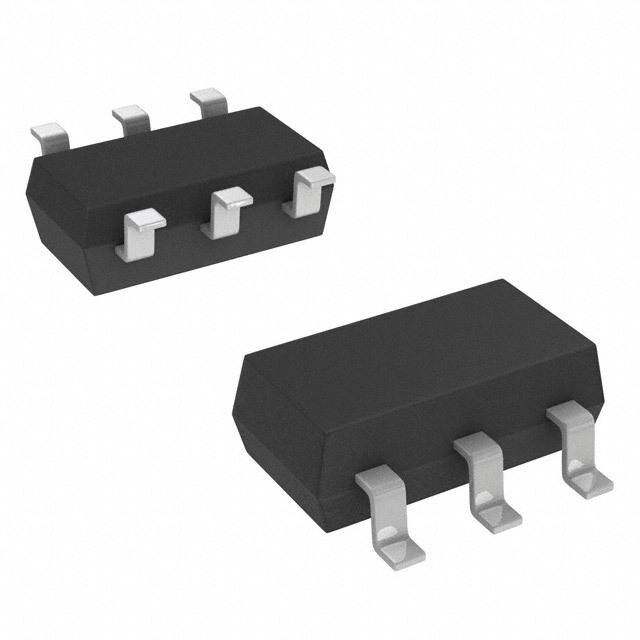
| 描述 | IC LED DRVR HP CONST TSOT23-6LED照明驱动器 1.6MHz, 1A Constant Current Buck LED Driver with Internal Compensation 6-SOT -40 to 125 |
| 产品分类 | |
| 品牌 | Texas Instruments |
| 产品手册 | |
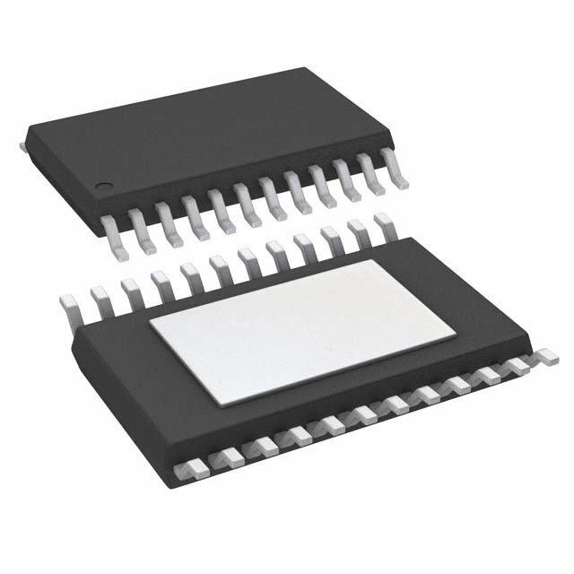
| 产品图片 |
|
| rohs | 符合RoHS无铅 / 符合限制有害物质指令(RoHS)规范要求 |
| 产品系列 | LED照明电子器件,LED照明驱动器,Texas Instruments LM3405AXMKE/NOPBPowerWise® |
| 数据手册 | |
| 产品型号 | LM3405AXMKE/NOPB |
| 产品培训模块 | http://www.digikey.cn/PTM/IndividualPTM.page?site=cn&lang=zhs&ptm=30139 |
| 产品种类 | LED照明驱动器 |
| 供应商器件封装 | TSOT-23-6 |
| 其它名称 | LM3405AXMKE |
| 内部驱动器 | 是 |
| 制造商产品页 | http://www.ti.com/general/docs/suppproductinfo.tsp?distId=10&orderablePartNumber=LM3405AXMKE/NOPB |
| 包装 | 带卷 (TR) |
| 参考设计库 | http://www.digikey.com/rdl/4294959899/4294959898/244 |
| 商标 | Texas Instruments |
| 安装类型 | 表面贴装 |
| 安装风格 | SMD/SMT |
| 宽度 | 1.65 mm |
| 封装 | Reel |
| 封装/外壳 | SOT-23-6 细型,TSOT-23-6 |
| 封装/箱体 | TSOT |
| 工作温度 | -40°C ~ 125°C |
| 工作频率 | 1.2 MHz to 1.9 MHz |
| 工厂包装数量 | 250 |
| 恒压 | - |
| 恒流 | 是 |
| 拓扑 | PWM,降压(降压) |
| 拓扑结构 | Buck |
| 最大工作温度 | + 125 C |
| 最大电源电流 | 2.8 mA |
| 最小工作温度 | - 40 C |
| 标准包装 | 250 |
| 电压-电源 | 3 V ~ 22 V |
| 电压-输出 | - |
| 类型 | Inductive |
| 类型-初级 | 闪灯/白光,通用 |
| 类型-次级 | 高亮度 LED(HBLED),白色 LED |
| 系列 | LM3405A |
| 设计资源 | http://www.digikey.com/product-highlights/cn/zh/texas-instruments-webench-design-center/3176 |
| 输入电压 | 3 V to 22 V |
| 输出数 | 1 |
| 输出电流 | 1 A |
| 输出端数量 | 1 Output |
| 输出类型 | Constant Current |
| 配用 | /product-detail/zh/LM3405AEVAL/LM3405AEVAL-ND/1738508 |
| 频率 | 1.2MHz ~ 1.9MHz |


- 商务部:美国ITC正式对集成电路等产品启动337调查
- 曝三星4nm工艺存在良率问题 高通将骁龙8 Gen1或转产台积电
- 太阳诱电将投资9.5亿元在常州建新厂生产MLCC 预计2023年完工
- 英特尔发布欧洲新工厂建设计划 深化IDM 2.0 战略
- 台积电先进制程称霸业界 有大客户加持明年业绩稳了
- 达到5530亿美元!SIA预计今年全球半导体销售额将创下新高
- 英特尔拟将自动驾驶子公司Mobileye上市 估值或超500亿美元
- 三星加码芯片和SET,合并消费电子和移动部门,撤换高东真等 CEO
- 三星电子宣布重大人事变动 还合并消费电子和移动部门
- 海关总署:前11个月进口集成电路产品价值2.52万亿元 增长14.8%


PDF Datasheet 数据手册内容提取
Product Sample & Technical Tools & Support & Folder Buy Documents Software Community LM3405A SNVS508D–OCTOBER2007–REVISEDSEPTEMBER2016 LM3405A 1.6-MHz, 1-A Constant Current Buck LED Driver With Internal Compensation in Tiny SOT and MSOP-PowerPAD™ Packages 1 Features 3 Description • V OperatingRangeof3Vto22V The LM3405A is a 1-A constant current buck LED 1 IN driver designed to provide a simple, high efficiency • Drivesupto5High-BrightnessLEDsinSeriesat solution for driving high power LEDs. With a 0.205-V 1A reference voltage feedback control to minimize power • ThinSOT-6andMSOP-PowerPAD™-8Packages dissipation, an external resistor sets the current as • 1.6-MHzSwitchingFrequency needed for driving various types of LEDs. Switching frequency is internally set to 1.6 MHz, allowing small • EN/DIMInputforEnablingandPWMDimmingof surface mount inductors and capacitors to be used. LEDs The LM3405A uses current-mode control and internal • 300-mΩ NMOSSwitch compensation offering ease of use and predictable, • 40-nAShutdownCurrentatV =5V high performance regulation over a wide range of IN operating conditions. With a maximum input voltage • InternallyCompensatedCurrent-modeControl of 22 V, the device can drive up to 5 High-Brightness • Cycle-by-CycleCurrentLimit LEDs in series at 1-A forward current, with the single • InputVoltageUVLO LED forward voltage of approximately 3.7 V. Additional features include user accessible EN/DIM • OvercurrentProtection pin for enabling and PWM dimming of LEDs, thermal • ThermalShutdown shutdown, cycle-by-cycle current limit and overcurrent protection. 2 Applications DeviceInformation(1) • LEDDrivers • ConstantCurrentSources PARTNUMBER PACKAGE BODYSIZE(NOM) SOT(6) 2.90mm×1.60mm • IndustrialLighting LM3405A MSOP-PowerPAD(8) 3.00mm×3.00mm • LEDFlashlights (1) For all available packages, see the orderable addendum at • LEDLightbulbs theendofthedatasheet. TypicalApplicationCircuit EfficiencyvsLEDCurrent(V =12V) IN D3 D2 VIN VIN BOOST C3 C1 L1 VOUT SW LM3405A ON D1 C2 C4 IF EN/DIM OFF FB GND R1 Copyright © 2016, Texas Instruments Incorporated 1 An IMPORTANT NOTICE at the end of this data sheet addresses availability, warranty, changes, use in safety-critical applications, intellectualpropertymattersandotherimportantdisclaimers.PRODUCTIONDATA.
LM3405A SNVS508D–OCTOBER2007–REVISEDSEPTEMBER2016 www.ti.com Table of Contents 1 Features.................................................................. 1 8 ApplicationandImplementation........................ 15 2 Applications........................................................... 1 8.1 ApplicationInformation............................................15 3 Description............................................................. 1 8.2 TypicalApplications................................................19 4 RevisionHistory..................................................... 2 8.3 SystemExamples...................................................21 5 PinConfigurationandFunctions......................... 3 9 PowerSupplyRecommendations...................... 25 6 Specifications......................................................... 4 10 Layout................................................................... 25 6.1 AbsoluteMaximumRatings .....................................4 10.1 LayoutGuidelines.................................................25 6.2 ESDRatings..............................................................4 10.2 LayoutExample....................................................25 6.3 RecommendedOperatingConditions.......................4 11 DeviceandDocumentationSupport................. 26 6.4 ThermalInformation..................................................5 11.1 DocumentationSupport........................................26 6.5 ElectricalCharacteristics...........................................5 11.2 ReceivingNotificationofDocumentationUpdates26 6.6 TypicalCharacteristics..............................................6 11.3 CommunityResource............................................26 7 DetailedDescription.............................................. 8 11.4 Trademarks...........................................................26 7.1 Overview...................................................................8 11.5 ElectrostaticDischargeCaution............................26 7.2 FunctionalBlockDiagram.........................................9 11.6 Glossary................................................................26 7.3 FeatureDescription...................................................9 12 Mechanical,Packaging,andOrderable Information........................................................... 26 7.4 DeviceFunctionalModes........................................14 4 Revision History NOTE:Pagenumbersforpreviousrevisionsmaydifferfrompagenumbersinthecurrentversion. ChangesfromRevisionC(May2013)toRevisionD Page • AddedESDRatingstable,FeatureDescriptionsection,DeviceFunctionalModes,ApplicationandImplementation section,PowerSupplyRecommendationssection,Layoutsection,DeviceandDocumentationSupportsection,and Mechanical,Packaging,andOrderableInformationsection ................................................................................................. 1 • ChangedR forSOTpackagefrom118°C/Wto182.9°C/W............................................................................................... 5 θJA • ChangedR forMSOPpackagefrom73°C/Wto55.3°C/W................................................................................................ 5 θJA ChangesfromRevisionB(April2013)toRevisionC Page • ChangedlayoutofNationalSemiconductorDataSheettoTIformat.................................................................................. 23 2 SubmitDocumentationFeedback Copyright©2007–2016,TexasInstrumentsIncorporated ProductFolderLinks:LM3405A
LM3405A www.ti.com SNVS508D–OCTOBER2007–REVISEDSEPTEMBER2016 5 Pin Configuration and Functions DDCPackage 6-PinSOT DGNPackage TopView 8-PinMSOP-PowerPAD™ TopView BOOST 1 6 SW FB 1 8 EN/DIM GND 2 7 GND GND 2 5 VIN NC 3 6 VIN FB 3 4 EN/DIM BOOST 4 5 SW PinFunctions PIN I/O DESCRIPTION NAME SOT MSOP-PowerPAD BoostvoltagethatdrivestheNMOSoutputswitch.Abootstrapcapacitoris BOOST 1 4 O connectedbetweentheBOOSTandSWpins. Signalandpowergroundpin.Placethebottomresistorofthefeedbacknetwork GND 2 2,7 — ascloseaspossibletothispin. Feedbackpin.ConnectFBtotheLEDstringcathodeandanexternalresistor FB 3 1 I togroundtosettheLEDcurrent. Enablecontrolinput.Logichighenablesoperation.Togglingthispinwitha periodiclogicsquarewaveofvaryingdutycycleatdifferentfrequencies EN/DIM 4 8 I controlsthebrightnessofLEDs.Donotallowthispintofloatorbegreaterthan V +0.3V. IN VIN 5 6 I Inputsupplyvoltage.ConnectabypasscapacitorlocallyfromthispintoGND. Switchpin.Connectthispintotheinductor,catchdiode,andbootstrap SW 6 5 O capacitor. NC — 3 — Noconnection. DAP N/A — — Attachtopowergroundpin(GND). Copyright©2007–2016,TexasInstrumentsIncorporated SubmitDocumentationFeedback 3 ProductFolderLinks:LM3405A
LM3405A SNVS508D–OCTOBER2007–REVISEDSEPTEMBER2016 www.ti.com 6 Specifications 6.1 Absolute Maximum Ratings overoperatingfree-airtemperaturerange(unlessotherwisenoted)(1) MIN MAX UNIT V –0.5 24 V IN SWvoltage –0.5 24 V Boostvoltage –0.5 30 V BoosttoSWvoltage –0.5 6 V FBvoltage –0.5 3 V EN/DIMvoltage –0.5 (V +0.3) V IN Junctiontemperature,T 150 °C J Storagetemperature,T –65 150 °C stg (1) StressesbeyondthoselistedunderAbsoluteMaximumRatingsmaycausepermanentdamagetothedevice.Thesearestressratings only,whichdonotimplyfunctionaloperationofthedeviceattheseoranyotherconditionsbeyondthoseindicatedunderRecommended OperatingConditions.Exposuretoabsolute-maximum-ratedconditionsforextendedperiodsmayaffectdevicereliability. 6.2 ESD Ratings VALUE UNIT LM3405AINSOTPACKAGE Human-bodymodel(HBM),perANSI/ESDA/JEDECJS-001(1) ±2000 V Electrostaticdischarge V (ESD) Charged-devicemodel(CDM),perJEDECspecificationJESD22-C101(2) ±1000 LM3405AINMSOP-PowerPADPACKAGE V Electrostaticdischarge Charged-devicemodel(CDM),perJEDECspecificationJESD22-C101(2) ±750 V (ESD) (1) JEDECdocumentJEP155statesthat500-VHBMallowssafemanufacturingwithastandardESDcontrolprocess. (2) JEDECdocumentJEP157statesthat250-VCDMallowssafemanufacturingwithastandardESDcontrolprocess. 6.3 Recommended Operating Conditions MIN MAX UNIT V 3 22 V IN EN/DIMvoltage 0 (V +0.3) V IN BoosttoSWvoltage 2.5 5.5 V Junctiontemperature –40 125 °C SOTpackage 400 mA I LED MSOP-PowerPADpackage 1 A 4 SubmitDocumentationFeedback Copyright©2007–2016,TexasInstrumentsIncorporated ProductFolderLinks:LM3405A
LM3405A www.ti.com SNVS508D–OCTOBER2007–REVISEDSEPTEMBER2016 6.4 Thermal Information LM3405A THERMALMETRIC(1) DDC DGN UNIT (SOT) (MSOP-PowerPAD) 6PINS 8PINS R Junction-to-ambientthermalresistance 182.9 55.3 °C/W θJA R Junction-to-case(top)thermalresistance 53.4 62.8 °C/W θJC(top) R Junction-to-boardthermalresistance 28.1 38.9 °C/W θJB ψ Junction-to-topcharacterizationparameter 1.2 8.2 °C/W JT ψ Junction-to-boardcharacterizationparameter 27.7 38.6 °C/W JB R Junction-to-case(bottom)thermalresistance N/A 8 °C/W θJC(bot) (1) Formoreinformationabouttraditionalandnewthermalmetrics,seetheSemiconductorandICPackageThermalMetricsapplication report. 6.5 Electrical Characteristics Unlessotherwisespecified,V =12V.TYPvaluesareforT =25°Conly;MIN/MAXlimitsapplyoverthejunction IN J temperature(T )rangeof–40°Cto125°C.Typicalvaluesrepresentthemostlikelyparametricnorm,andareprovidedfor J referencepurposesonly. PARAMETER TESTCONDITIONS MIN TYP MAX UNIT V Feedbackvoltage 0.188 0.205 0.22 V FB Feedbackvoltageline ΔV /(ΔV xV ) V =3Vto22V 0.01 %/V FB IN FB regulation IN Feedbackinputbias I Sink/source 10 250 nA FB current V Rising 2.74 2.95 V IN Undervoltagelockout UVLO V Falling 1.9 2.3 V IN UVLOHysteresis 0.44 V f Switchingfrequency 1.2 1.6 1.9 MHz SW D Maximumdutycycle V =0V 85% 94% MAX FB SOT(V -V =3V) 300 600 BOOST SW R SwitchONresistance mΩ DS(ON) MSOP-PowerPAD(V -V =3V) 360 700 BOOST SW I Switchcurrentlimit V -V =3V,V =3V 1.2 2 2.8 A CL BOOST SW IN Quiescentcurrent Switching,V =0.195V 1.8 2.8 mA FB IQ Quiescentcurrent V =0V 0.3 µA (shutdown) EN/DIM Enablethresholdvoltage V Rising 1.8 V EN/DIM VEN/DIM_TH Shutdownthreshold V Falling 0.4 V voltage EN/DIM I EN/DIMpincurrent Sink/Source 0.01 µA EN/DIM I Switchleakage V =22V 0.1 µA SW IN Copyright©2007–2016,TexasInstrumentsIncorporated SubmitDocumentationFeedback 5 ProductFolderLinks:LM3405A
LM3405A SNVS508D–OCTOBER2007–REVISEDSEPTEMBER2016 www.ti.com 6.6 Typical Characteristics Unlessotherwisespecified,V =12V,V –V =5VandT =25°C. IN BOOST SW A VIN=5V IF=1A Figure1. EfficiencyvsLEDCurrent Figure2.EfficiencyvsInputVoltage I =0.7A I =0.35A F F Figure3.EfficiencyvsInputVoltage Figure4.EfficiencyvsInputVoltage Figure5.V vsTemperature Figure6.OscillatorFrequencyvsTemperature FB 6 SubmitDocumentationFeedback Copyright©2007–2016,TexasInstrumentsIncorporated ProductFolderLinks:LM3405A
LM3405A www.ti.com SNVS508D–OCTOBER2007–REVISEDSEPTEMBER2016 Typical Characteristics (continued) Unlessotherwisespecified,V =12V,V –V =5VandT =25°C. IN BOOST SW A V -V =3V BOOST SW Figure7.CurrentLimitvsTemperature Figure8.SOTR vsTemperature DS(ON) V =15V I =0.2A IN F Figure10.Start-UpResponsetoEN/DIMSignal Figure9.QuiescentCurrentvsTemperature Copyright©2007–2016,TexasInstrumentsIncorporated SubmitDocumentationFeedback 7 ProductFolderLinks:LM3405A
LM3405A SNVS508D–OCTOBER2007–REVISEDSEPTEMBER2016 www.ti.com 7 Detailed Description 7.1 Overview The LM3405A is a PWM, current-mode controlled buck switching regulator designed to provide a simple, high efficiency solution for driving LEDs with a preset switching frequency of 1.6MHz. This high frequency allows the LM3405A to operate with small surface mount capacitors and inductors, resulting in LED drivers that need only a minimum amount of board space. The LM3405A is internally compensated, simple to use, and requires few externalcomponents. ThefollowingdescriptionofoperationoftheLM3405Areferstothe Typical Application Circuit and to the waveforms in Figure 11. The LM3405A supplies a regulated output current by switching the internal NMOS power switch at constant frequency and variable duty cycle. A switching cycle begins at the falling edge of the reset pulse generated by the internal oscillator. When this pulse goes low, the output control logic turns on the internal NMOS power switch. During this on-time, the SW pin voltage (V ) SW swings up to approximately V , and the inductor current (I ) increases with a linear slope. I is measured by the IN L L current sense amplifier, which generates an output proportional to the switch current. The sense signal is summed with the regulator’s corrective ramp and compared to the error amplifier’s output, which is proportional to the difference between the feedback voltage and V . When the PWM comparator output goes high, the REF internal power switch turns off until the next switching cycle begins. During the switch off-time, inductor current discharges through the catch diode D1, which forces the SW pin to swing below ground by the forward voltage (V ) of the catch diode. The regulator loop adjusts the duty cycle (D) to maintain a constant output current (I ) D1 F throughtheLED,byforcingFBpinvoltagetobeequaltoV (0.205V). REF VSW D = TON/TSW VIN SW Voltage TON TOFF 0 -VD1 t TSW IL ILPK IF ’iL Inductor Current 0 t Figure11. SWPinVoltageandInductorCurrentWaveformsofLM3405A 8 SubmitDocumentationFeedback Copyright©2007–2016,TexasInstrumentsIncorporated ProductFolderLinks:LM3405A
LM3405A www.ti.com SNVS508D–OCTOBER2007–REVISEDSEPTEMBER2016 7.2 Functional Block Diagram Copyright © 2016, Texas Instruments Incorporated 7.3 Feature Description 7.3.1 BoostFunction Capacitor C3 and diode D2 in the Functional Block Diagram are used to generate a voltage V . The voltage BOOST across C3, V - V , is the gate drive voltage to the internal NMOS power switch. To properly drive the BOOST SW internal NMOS switch during its on-time, V needs to be at least 2.5-V greater than V . A large value of BOOST SW V - V is recommended to achieve better efficiency by minimizing both the internal switch ON resistance BOOST SW (R ), and the switch rise and fall times. However, V - V should not exceed the maximum operating DS(ON) BOOST SW limitof5.5V. When the LM3405A starts up, internal circuitry from V supplies a 20-mA current to the BOOST pin, flowing out IN of the BOOST pin into C3. This current charges C3 to a voltage sufficient to turn the switch on. The BOOST pin willcontinuetosourcecurrenttoC3untilthevoltageatthefeedbackpinisgreaterthan123mV. TherearevariousmethodstoderiveV : BOOST 1. Fromtheinputvoltage(V ) IN 2. Fromtheoutputvoltage(V ) OUT 3. FromashuntorseriesZenerdiode 4. Fromanexternaldistributedvoltagerail(V ) EXT The first method is shown in the Functional Block Diagram. Capacitor C3 is charged via diode D2 by V . During IN a normal switching cycle, when the internal NMOS power switch is off (T ) (see Figure 11), V equals V OFF BOOST IN minus the forward voltage of D2 (V ), during which the current in the inductor (L1) forward biases the catch D2 diodeD1(V ).ThereforethegatedrivevoltagestoredacrossC3is: D1 V -V =V -V +V (1) BOOST SW IN D2 D1 WhentheNMOSswitchturnson(T ),theswitchpinrisesto: ON V =V –(R ×I ) (2) SW IN DS(ON) L Copyright©2007–2016,TexasInstrumentsIncorporated SubmitDocumentationFeedback 9 ProductFolderLinks:LM3405A
LM3405A SNVS508D–OCTOBER2007–REVISEDSEPTEMBER2016 www.ti.com Feature Description (continued) SincethevoltageacrossC3remainsunchanged,V isforcedtorisethusreversebiasingD2.Thevoltageat BOOST V isthen: BOOST V =2V –(R ×I )–V +V (3) BOOST IN DS(ON) L D2 D1 Depending on the quality of the diodes D1 and D2, the gate drive voltage in this method can be slightly less or larger than the input voltage V . For best performance, ensure that the variation of the input supply does not IN causethegatedrivevoltagetofalloutsidetherecommendedrange: 2.5V<V -V +V <5.5V (4) IN D2 D1 ThesecondmethodforderivingtheboostvoltageistoconnectD2totheoutputasshowninFigure12.Thegate drivevoltageinthisconfigurationis: V -V =V –V +V (5) BOOST SW OUT D2 D1 Since the gate drive voltage needs to be in the range of 2.5 V to 5.5 V, the output voltage V should be limited OUT toacertainrange.ForthecalculationofV ,seeOutputVoltage. OUT Copyright © 2016, Texas Instruments Incorporated Figure12. V DerivedfromV BOOST OUT The third method can be used in the applications where both V and V are greater than 5.5 V. In these IN OUT cases, C3 cannot be charged directly from these voltages; instead C3 can be charged from V or V minus a IN OUT Zener voltage (V ) by placing a Zener diode D3 in series with D2 as shown in Figure 13. When using a series D3 Zenerdiodefromtheinput,thegatedrivevoltageisV -V -V +V . IN D3 D2 D1 Copyright © 2016, Texas Instruments Incorporated Figure13. V DerivedfromV ThroughaSeriesZener BOOST IN 10 SubmitDocumentationFeedback Copyright©2007–2016,TexasInstrumentsIncorporated ProductFolderLinks:LM3405A
LM3405A www.ti.com SNVS508D–OCTOBER2007–REVISEDSEPTEMBER2016 Feature Description (continued) An alternate method is to place the zener diode D3 in a shunt configuration as shown in Figure 14. A small 350 mW to 500 mW, 5.1-V Zener in a SOT or SOD package can be used for this purpose. A small ceramic capacitor such as a 6.3 V, 0.1-µF capacitor (C5) should be placed in parallel with the Zener diode. When the internal NMOS switch turns on, a pulse of current is drawn to charge the internal NMOS gate capacitance. The 0.1-µF parallel shunt capacitor ensures that the V voltage is maintained during this time. Resistor R2 should be BOOST chosentoprovideenoughRMScurrenttothezenerdiodeandtotheBOOSTpin.Arecommendedchoiceforthe zener current (I ) is 1 mA. The current I into the BOOST pin supplies the gate current of the NMOS ZENER BOOST power switch. It reaches a maximum of around 3.6 mA at the highest gate drive voltage of 5.5 V over the LM3405Aoperatingrange. FortheworstcaseI ,increasethecurrentby50%.Inthatcase,themaximumboostcurrentwillbe: BOOST I =1.5×3.6mA=5.4mA (6) BOOST-MAX R2willthenbegivenby: R2=(V -V )/(I +I ) (7) IN ZENER BOOST_MAX ZENER Forexample,letV =12V,V =5V,I =1mA,then: IN ZENER ZENER R2=(12V–5V)/(5.4mA+1mA)=1.09kΩ (8) Copyright © 2016, Texas Instruments Incorporated Figure14. V DerivedfromV ThroughaShuntZener BOOST IN Thefourthmethodcanbeusedinanapplicationwhichhasanexternallowvoltagerail,V .C3canbecharged EXT through D2 from V , independent of V and V voltage levels. Again for best performance, ensure that the EXT IN OUT gatedrivevoltage,V -V +V ,fallsintherangeof2.5Vto5.5V. EXT D2 D1 7.3.2 SettingtheLEDCurrent LM3405A is a constant current buck regulator. The LEDs are connected between V and the FB pin as shown OUT inthe Typical Application Circuit. The FB pin is at 0.205V in regulation and therefore the LED current I is set by V F FB andresistorR1fromFBtogroundbythefollowingequation: I =V /R1 (9) F FB I should not exceed the 1-A current capability of LM3405A and therefore R1 minimum must be approximately F 0.2 Ω. I should also be kept above 200 mA for stable operation, and therefore R1 maximum must be F approximately 1 Ω. If average LED currents less than 200 mA are desired, the EN/DIM pin can be used for PWM dimming.SeeLEDPWMDimming. 7.3.3 OutputVoltage The output voltage is primarily determined by the number of LEDs (n) connected from V to FB pin and OUT thereforeV canbewrittenas: OUT V =((n×V )+V ) OUT F FB Copyright©2007–2016,TexasInstrumentsIncorporated SubmitDocumentationFeedback 11 ProductFolderLinks:LM3405A
LM3405A SNVS508D–OCTOBER2007–REVISEDSEPTEMBER2016 www.ti.com Feature Description (continued) where • V istheforwardvoltageofoneLEDatthesetLEDcurrentlevel(seeLEDmanufacturerdatasheetfor F forwardcharacteristicscurve) (10) 7.3.4 EnableMode/ShutdownMode The LM3405A has both enable and shutdown modes that are controlled by the EN/DIM pin. Connecting a voltage source greater than 1.8 V to the EN/DIM pin enables the operation of LM3405A, while reducing this voltage below 0.4 V places the part in a low quiescent current (0.3 µA typical) shutdown mode. There is no internalpulluponEN/DIMpin,thereforeanexternalsignalisrequiredtoinitiateswitching.Donotallowthispinto float or rise to 0.3 V above V . It should be noted that when the EN/DIM pin voltage rises above 1.8 V while the IN input voltage is greater than UVLO, there is a finite delay before switching starts. During this delay the LM3405A will go through a power on reset state after which the internal soft-start process commences. The soft-start process limits the inrush current and brings up the LED current (I ) in a smooth and controlled fashion. The total F combined duration of the power on reset delay, soft-start delay and the delay to fully establish the LED current is intheorderof100µs(seeFigure19). ThesimplestwaytoenabletheoperationofLM3405AistoconnecttheEN/DIMpintoV whichallowsselfstart- IN up of LM3405A whenever the input voltage is applied. However, when an input voltage of slow rise time is used to power the application and if both the input voltage and the output voltage are not fully established before the soft-start time elapses, the control circuit will command maximum duty cycle operation of the internal power switch to bring up the output voltage rapidly. When the feedback pin voltage exceeds 0.205 V, the duty cycle will have to reduce from the maximum value accordingly, to maintain regulation. It takes a finite amount of time for this reduction of duty cycle and this will result in a spike in LED current for a short duration as shown in Figure 15. In applications where this LED current overshoot is undesirable, EN/DIM pin voltage can be separately applied and delayed such that V is fully established before the EN/DIM pin voltage reaches the IN enable threshold. The effect of delaying EN/DIM with respect to V on the LED current is shown in Figure 16. IN For a fast rising input voltage (200 µs for example), there is no need to delay the EN/DIM signal since soft-start cansmoothlybringuptheLEDcurrentasshowninFigure17. Figure15.Start-UpResponsetoVINWith5-msRiseTime Figure16.Start-UpResponsetoVINWithEN/DIMDelayed 12 SubmitDocumentationFeedback Copyright©2007–2016,TexasInstrumentsIncorporated ProductFolderLinks:LM3405A
LM3405A www.ti.com SNVS508D–OCTOBER2007–REVISEDSEPTEMBER2016 Feature Description (continued) Figure17.Start-UpResponsetoV With200-µsRiseTime IN 7.3.5 LEDPWMDimming The LED brightness can be controlled by applying a periodic pulse signal to the EN/DIM pin and varying its frequency and/or duty cycle. This so-called PWM dimming method controls the average light output by pulsing the LED current between the set value and zero. A logic high level at the EN/DIM pin turns on the LED current whereas a logic low level turns off the LED current. Figure 18 shows a typical LED current waveform in PWM dimming mode. As explained in the previous section, there is approximately a 100-µs delay from the EN/DIM signal going high to fully establishing the LED current as shown in Figure 19. This 100-µs delay sets a maximum frequency limit for the driving signal that can be applied to the EN/DIM pin for PWM dimming. Figure 20 shows the average LED current versus duty cycle of PWM dimming signal for various frequencies. The applicable frequency range to drive LM3405A for PWM dimming is from 100 Hz to 5 kHz. The dimming ratio reduces drasticallywhentheappliedPWMdimmingfrequencyisgreaterthan5kHz. Figure18.PWMDimmingofLEDs Figure19.Start-UpResponsetoEN/DIM UsingtheEN/DIMPin WithI =1A F Copyright©2007–2016,TexasInstrumentsIncorporated SubmitDocumentationFeedback 13 ProductFolderLinks:LM3405A
LM3405A SNVS508D–OCTOBER2007–REVISEDSEPTEMBER2016 www.ti.com Feature Description (continued) Figure20.AverageLEDCurrentvs DutyCycleofPWMDimmingSignalatEN/DIMPin 7.3.6 UndervoltageLockout Undervoltage lockout (UVLO) prevents the LM3405A from operating until the input voltage exceeds 2.74 V (typical). The UVLO threshold has approximately 440 mV of hysteresis, so the part will operate until V drops IN below2.3V(typical).HysteresispreventsthepartfromturningoffduringpowerupifV isnon-monotonic. IN 7.3.7 CurrentLimit The LM3405A uses cycle-by-cycle current limit to protect the internal power switch. During each switching cycle, a current limit comparator detects if the power switch current exceeds 2 A (typical), and turns off the switch until thenextswitchingcyclebegins. 7.3.8 OvercurrentProtection The LM3405A has a built-in overcurrent comparator that compares the FB pin voltage to a threshold voltage that is 60% higher than the internal reference V . Once the FB pin voltage exceeds this threshold level (typically REF 328 mV), the internal NMOS power switch is turned off, which allows the feedback voltage to decrease towards regulation. This threshold provides an upper limit for the LED current. LED current overshoot is limited to 328 mV/R1bythiscomparatorduringtransients. 7.4 Device Functional Modes 7.4.1 ThermalShutdown Thermal shutdown limits total power dissipation by turning off the internal power switch when the IC junction temperature exceeds 165°C. After thermal shutdown occurs, the power switch does not turn on until the junction temperaturedropsbelowapproximately150°C. 14 SubmitDocumentationFeedback Copyright©2007–2016,TexasInstrumentsIncorporated ProductFolderLinks:LM3405A
LM3405A www.ti.com SNVS508D–OCTOBER2007–REVISEDSEPTEMBER2016 8 Application and Implementation NOTE Information in the following applications sections is not part of the TI component specification, and TI does not warrant its accuracy or completeness. TI’s customers are responsible for determining suitability of components for their purposes. Customers should validateandtesttheirdesignimplementationtoconfirmsystemfunctionality. 8.1 Application Information 8.1.1 Inductor(L1) TheDutyCycle(D)canbeapproximatedquicklyusingtheratioofoutputvoltage(V )toinputvoltage(V ): OUT IN VOUT D = VIN (11) The catch diode (D1) forward voltage drop and the voltage drop across the internal NMOS must be included to calculateamoreaccuratedutycycle.CalculateDbyusingEquation12: VOUT + VD1 D = VIN + VD1 - VSW (12) V canbeapproximatedbyEquation13: SW V =I ×R (13) SW F DS(ON) The diode forward drop (V ) can range from 0.3 V to 0.7 V depending on the quality of the diode. The lower V D1 D1 is,thehighertheoperatingefficiencyoftheconverter. The inductor value determines the output ripple current (Δi , as defined in Figure 11). Lower inductor values L decrease the size of the inductor, but increases the output ripple current. An increase in the inductor value will decrease the output ripple current. The ratio of ripple current to LED current is optimized when it is set between 0.3and0.4at1ALEDcurrent.Thisratiorisdefinedas: ’iL r = lF (14) One must also ensure that the minimum current limit (1.2 A) is not exceeded, so the peak current in the inductor mustbecalculated.Thepeakcurrent(I )intheinductoriscalculatedas: LPK I =I +Δi /2 (15) LPK F L When the designed maximum output current is reduced, the ratio r can be increased. At a current of 0.2 A, r can be made as high as 0.7. The ripple ratio can be increased at lighter loads because the net ripple is actually quite low, and if r remains constant the inductor value can be made quite large. An equation empirically developed for themaximumrippleratioatanycurrentbelow2Ais: r=0.387×I –0.3667 (16) OUT Notethatthisisjustaguideline. The LM3405A operates at a high frequency allowing the use of ceramic output capacitors without compromising transient response. Ceramic capacitors allow higher inductor ripple without significantly increasing LED current ripple.Seetheoutputcapacitorandfeed-forwardcapacitorsectionsformoredetailsonLEDcurrentripple. Nowthattheripplecurrentorrippleratioisdetermined,theinductanceiscalculatedbyEquation17: VOUT + VD1 L = x (1-D) IF x r x fSW where • f istheswitchingfrequency SW • I istheLEDcurrent (17) F Copyright©2007–2016,TexasInstrumentsIncorporated SubmitDocumentationFeedback 15 ProductFolderLinks:LM3405A
LM3405A SNVS508D–OCTOBER2007–REVISEDSEPTEMBER2016 www.ti.com Application Information (continued) When selecting an inductor, make sure that it is capable of supporting the peak output current without saturating. Inductor saturation will result in a sudden reduction in inductance and prevent the regulator from operating correctly. Because of the operating frequency of the LM3405A, ferrite based inductors are preferred to minimize core losses. This presents little restriction since the variety of ferrite based inductors is huge. Lastly, inductors with lower series resistance (DCR) will provide better operating efficiency. For recommended inductor selection, refertoCircuitExamplesandRecommendedInductanceRangeinTable1. Table1.RecommendedInductanceRange I INDUCTANCERANGEANDINDUCTORCURRENTRIPPLE F 6.8µH-15µH 1A Inductance 6.8µH 10µH 15µH Δi /I (1) 51% 36% 24% L F 10µH-22µH 0.6A Inductance 10µH 15µH 22µH Δi /I (1) 58% 39% 26% L F 15µH-27µH 0.2A Inductance 15µH 22µH 27µH Δi /I (1) 116% 79% 65% L F (1) MaximumoverfullrangeofV andV . IN OUT 8.1.2 InputCapacitor(C1) An input capacitor is necessary to ensure that V does not drop excessively during switching transients. The IN primary specifications of the input capacitor are capacitance, voltage rating, RMS current rating, and ESL (Equivalent Series Inductance). The input voltage rating is specifically stated by the capacitor manufacturer. Make sure to check any recommended deratings and also verify if there is any significant change in capacitance at the operating input voltage and the operating temperature. The input capacitor maximum RMS input current rating(I )mustbegreaterthan: RMS-IN IRMS-IN = IF x D x 1 - D +1r22 (18) It can be shown from the above equation that maximum RMS capacitor current occurs when D = 0.5. Always calculate the RMS at the point where the duty cycle D, is closest to 0.5. The ESL of an input capacitor is usually determined by the effective cross sectional area of the current path. A large leaded capacitor will have high ESL and an 0805 ceramic chip capacitor will have very low ESL. At the operating frequency of the LM3405A, certain capacitors may have an ESL so large that the resulting inductive impedance (2πfL) will be higher than that required to provide stable operation. It is strongly recommended to use ceramic capacitors due to their low ESR and low ESL. A 10µF multilayer ceramic capacitor (MLCC) is a good choice for most applications. In cases where large capacitance is required, use surface mount capacitors such as Tantalum capacitors and place at least a 1µF ceramic capacitor close to the V pin. For MLCCs it is recommended to use X7R or X5R dielectrics. IN Consultcapacitormanufacturerdatasheettoseehowratedcapacitancevariesoveroperatingconditions. 8.1.3 OutputCapacitor(C2) TheoutputcapacitorisselectedbaseduponthedesiredreductioninLEDcurrentripple.A1µFceramiccapacitor results in very low LED current ripple for most applications. Due to the high switching frequency, the 1µF capacitor alone (without feed-forward capacitor C4) can filter more than 90% of the inductor current ripple for most applications where the sum of LED dynamic resistance and R1 is larger than 1Ω. Since the internal compensation is tailored for small output capacitance with very low ESR, it is strongly recommended to use a ceramiccapacitorwithcapacitancelessthan3.3µF. 16 SubmitDocumentationFeedback Copyright©2007–2016,TexasInstrumentsIncorporated ProductFolderLinks:LM3405A
LM3405A www.ti.com SNVS508D–OCTOBER2007–REVISEDSEPTEMBER2016 Given the availability and quality of MLCCs and the expected output voltage of designs using the LM3405A, there is really no need to review other capacitor technologies. A benefit of ceramic capacitors is their ability to bypass high frequency noise. A certain amount of switching edge noise will couple through the parasitic capacitances in the inductor to the output. A ceramic capacitor will bypass this noise. In cases where large capacitance is required, use Electrolytic or Tantalum capacitors with large ESR, and verify the loop performance on the bench. Like the input capacitor, multilayer ceramic capacitors are recommended X7R or X5R. Again, verifyactualcapacitanceatthedesiredoperatingvoltageandtemperature. ChecktheRMScurrentratingofthecapacitor.ThemaximumRMScurrentratingofthecapacitoris: r IRMS-OUT = IF x 12 (19) One may select a 1206 size ceramic capacitor for C2 since its current rating is typically higher than 1A, more thanenoughfortherequirement. 8.1.4 Feed-ForwardCapacitor(C4) The feed-forward capacitor (designated as C4) connected in parallel with the LED string is required to provide multiple benefits to the LED driver design. It greatly improves the large signal transient response and suppresses LED current overshoot that may otherwise occur during PWM dimming; it also helps to shape the rise and fall times of the LED current pulse during PWM dimming thus reducing EMI emission; it reduces LED current ripple by bypassing some of inductor ripple from flowing through the LED. For most applications, a 1-µF ceramic capacitor is sufficient. In fact, the combination of a 1µF feed-forward ceramic capacitor and a 1µF output ceramic capacitorleadstolessthan1%currentrippleflowingthroughtheLED.LowerandhigherC4valuescanbeused, butbenchvalidationisrequiredtoensuretheperformancemeetstheapplicationrequirement. Figure 21 shows a typical LED current waveform during PWM dimming without feed-forward capacitor. At the beginning of each PWM cycle, overshoot can be seen in the LED current. Adding a 1µF feed-forward capacitor cantotallyremovetheovershootasshowninFigure22. Figure21.PWMDimmingWithoutFeed-ForwardCapacitor Figure22.PWMDimmingWitha1-µFFeed-Forward Capacitor 8.1.5 CatchDiode(D1) The catch diode (D1) conducts during the switch off-time. A Schottky diode is required for its fast switching time andlowforwardvoltagedrop.Thecatchdiodeshouldbechosensuchthatitscurrentratingisgreaterthan: I =I ×(1-D) (20) D1 F The reverse breakdown rating of the diode must be at least the maximum input voltage plus appropriate margin. Toimproveefficiency,chooseaSchottkydiodewithalowforwardvoltagedrop. Copyright©2007–2016,TexasInstrumentsIncorporated SubmitDocumentationFeedback 17 ProductFolderLinks:LM3405A
LM3405A SNVS508D–OCTOBER2007–REVISEDSEPTEMBER2016 www.ti.com 8.1.6 BoostDiode(D2) A standard diode such as the 1N4148 type is recommended. For V circuits derived from voltages less than BOOST 3.3V, a small-signal Schottky diode is recommended for better efficiency. A good choice is the BAT54 small signaldiode. 8.1.7 BoostCapacitor(C3) A 0.01µF ceramic capacitor with a voltage rating of at least 6.3V is sufficient. The X7R and X5R MLCCs provide thebestperformance. 8.1.8 PowerLossEstimation ThemainpowerlossinLM3405Aincludesthreebasictypesoflossintheinternalpowerswitch:conductionloss, switching loss, and gate charge loss. In addition, there is loss associated with the power required for the internal circuitryofIC. Theconductionlossiscalculatedas: § 2• PCOND (cid:11)IF2 uD(cid:12)u¤1(cid:14) 1u§¤’iL •‚ ‚uRDS(ON) ¤' 3 ' IF „ ‚„ (21) Iftheinductorripplecurrentisfairlysmall(forexample,lessthan40%),theconductionlosscanbesimplifiedto: P =I 2xR xD (22) COND F DS(ON) The switching loss occurs during the switch on and off transition periods, where voltage and current overlap resulting in power loss. The simplest means to determine this loss is to empirically measure the rise and fall times(10%to90%)ofthevoltageattheswitchpin. Switchingpowerlossiscalculatedasfollows: P =0.5xV xI xf x(T +T ) (23) SW IN F SW RISE FALL ThegatechargelossisassociatedwiththegatechargeQ requiredtodrivetheswitch: G P =f xV xQ (24) G SW IN G Thepowerlossrequiredforoperationoftheinternalcircuitry: P =I xV (25) Q Q IN I isthequiescentoperatingcurrent,andistypicallyaround1.8mAfortheLM3405A. Q ThetotalpowerlossintheICis: P =P +P +P +P (26) INTERNAL COND SW G Q AnexampleofpowerlossesforatypicalapplicationisshowninTable2: Table2.PowerLossTabulation CONDITIONS POWERLOSS V 12V IN V 3.9V OUT I 1A OUT V 0.45V D1 R 300mΩ P 108mW DS(ON) COND f 1.6MHz SW T 18ns RISE P 288mW SW T 12ns FALL I 1.8mA P 22mW Q Q Q 1.4nC P 27mW G G Discalculatedtobe0.36 18 SubmitDocumentationFeedback Copyright©2007–2016,TexasInstrumentsIncorporated ProductFolderLinks:LM3405A
LM3405A www.ti.com SNVS508D–OCTOBER2007–REVISEDSEPTEMBER2016 Σ(P +P +P +P )=P (27) COND SW Q G INTERNAL P =445mW (28) INTERNAL 8.2 Typical Applications 8.2.1 V DerivedfromV (V =5V,I =1A) BOOST IN IN F D2 VIN VIN BOOST C3 C1 L1 VOUT SW LM3405A D1 C2 DC or C4 LED1 IF EN/DIM PWM FB GND R1 Copyright © 2016, Texas Instruments Incorporated Figure23. V DerivedfromV BOOST IN (V =5V,I =1A)Diagram IN F 8.2.1.1 DesignRequirements • InputVoltage:V =5V± 10% IN • LEDCurrent:I =1A F • LEDForwardVoltage:V =3.4V LED • OutputVoltage:VOUT=3.4V+0.2V=3.6V • RippleRatio:r< 0.6 • PWMDimmable 8.2.1.2 DetailedDesignProcedure 8.2.1.2.1 CalculateDutyCycle(D) Calculate the nominal duty cycle for calculations and ensure the maximum duty cycle will not be exceeded in the applicationusingEquation29: V 3.6V D = OUT = = 0.72 V 5V IN (29) Using the same equation D can be calculated for the minimum input voltage of 4.5 V. The duty cycle at 4.5 V MAX is0.8whichislessthantheminimumD of0.85specifiedinElectricalCharacteristics. MAX 8.2.1.2.2 ChooseCapacitorValues(C1,C2,C3,andC4) Low input voltage applications and PWM dimming applications generally require more input capacitance so the higher value of C1 = 10 µF is chosen for best performance. The other capacitor values chosen are the recommended values of C2 = C4 = 1 µF and C3 = 0.01 µF. All capacitors chosen are X5R or X7R dielectric ceramiccapacitorsofsufficientvoltagerating. 8.2.1.2.3 SettheNominalLEDCurrent(R1) ThenominalLEDcurrentat100%PWMdimmingdutycycleissetbytheresistorR1.R1canbecalculatedusing Equation30: V 0.205V R1 = FB = = 0.205(cid:13) I 1A F (30) Copyright©2007–2016,TexasInstrumentsIncorporated SubmitDocumentationFeedback 19 ProductFolderLinks:LM3405A
LM3405A SNVS508D–OCTOBER2007–REVISEDSEPTEMBER2016 www.ti.com Typical Applications (continued) ThestandardvalueofR1=0.2Ωischosen.R1shouldhaveapowerratingofatleast1/4W. 8.2.1.2.4 ChooseDiodes(D1andD2) For the boost diode, D2, choose a low current diode with a voltage rating greater than the input voltage to give some margin. D2 should also be a schottky to minimize the forward voltage drop. For this example a schottky diode of D2 = 100 mA, 30 V is chosen. The catch diode, D1, should be a schottky diode and should have a voltage rating greater than the input voltage and a current rating greater than the average current. The average currentinD1canbecalculatedwithEquation31: I = I × :1 - D; = 1A × :1 - 0.72; = 0.28A D1 F (31) ForthisexampleD1=1A,10Vischosen. 8.2.1.2.5 CalculatetheInductorValue(L1) The inductor value is chosen for a given ripple ratio (r). To calculate L1 the forward voltage of D1 is required. In this case the chosen diode has a forward voltage drop of V = 0.37 V. Given the desired ripple ratio L1 is F calculatedas: V + V 3.6V + 0.37V L = OUT D1 = = 4.1(cid:23)(cid:29)H I × r × f 1A × 0.6 × 1.6MHz F SW (32) The next larger standard value of L1 = 4.7 µH is chosen. A ripple ratio of 0.6 translates to a Δi of 600 mA and a L peakinductorcurrentof1.3A(I +Δi /2).Chooseaninductorwithasaturationcurrentratingofgreaterthan F L 1.3A. Table3.BillofMaterialsforFigure23 PARTID PARTVALUE PARTNUMBER MANUFACTURER U1 1-ALEDDriver LM3405A TexasInstruments C1,InputCap 10µF,6.3V,X5R C3216X5R0J106M TDK C2,OutputCap 1µF,10V,X7R GRM319R71A105KC01D Murata C3,BoostCap 0.01µF,16V,X7R 0805YC103KAT2A AVX C4,FeedforwardCap 1µF,10V,X7R GRM319R71A105KC01D Murata D1,CatchDiode Schottky,0.37Vat1A,V =10V MBRM110LT1G ONSemiconductor R D2,BoostDiode Schottky,0.36Vat15mA CMDSH-3 CentralSemiconductor L1 4.7µH,1.6A SLF6028T-4R7M1R6 TDK R1 0.2Ω,0.5W,1% WSL2010R2000FEA Vishay LED1 1.5A,WhiteLED LXK2-PW14 Lumileds 8.2.1.3 ApplicationCurve Figure24.EfficiencyvsInputVoltage 20 SubmitDocumentationFeedback Copyright©2007–2016,TexasInstrumentsIncorporated ProductFolderLinks:LM3405A
LM3405A www.ti.com SNVS508D–OCTOBER2007–REVISEDSEPTEMBER2016 8.3 System Examples 8.3.1 V DerivedfromV (V =12V,I =1A) BOOST OUT IN F D2 VIN VIN BOOST C3 C1 L1 VOUT SW LM3405A D1 C2 DC or EN/DIM C4 LED1 IF PWM FB GND R1 Copyright © 2016, Texas Instruments Incorporated Figure25. V DerivedfromV BOOST OUT (V =12V,I =1A)Diagram IN F Table4.BillofMaterialsforFigure25 PARTID PARTVALUE PARTNUMBER MANUFACTURER U1 1-ALEDDriver LM3405A TexasInstruments C1,InputCap 10µF,25V,X5R ECJ-3YB1E106K Panasonic C2,OutputCap 1µF,10V,X7R GRM319R71A105KC01D Murata C3,BoostCap 0.01µF,16V,X7R 0805YC103KAT2A AVX C4,FeedforwardCap 1µF,10V,X7R GRM319R71A105KC01D Murata D1,CatchDiode Schottky,0.5Vat1A,V =30V SS13 Vishay R D2,BoostDiode Schottky,0.36Vat15mA CMDSH-3 CentralSemiconductor L1 4.7µH,1.6A SLF6028T-4R7M1R6 TDK R1 0.2Ω,0.5W,1% WSL2010R2000FEA Vishay LED1 1.5A,WhiteLED LXK2-PW14 Lumileds 8.3.2 V DerivedfromV throughaSeriesZenerDiode(D3)(V =15V,I =1A) BOOST IN IN F D3 D2 VIN VIN BOOST C3 C1 L1 VOUT SW LM3405A D1 C2 DC or C4 LED1 IF EN/DIM PWM FB GND R1 Copyright © 2016, Texas Instruments Incorporated Figure26. V DerivedfromV throughaSeriesZenerDiode(D3) BOOST IN (V =15V,I =1A)Diagram IN F Copyright©2007–2016,TexasInstrumentsIncorporated SubmitDocumentationFeedback 21 ProductFolderLinks:LM3405A
LM3405A SNVS508D–OCTOBER2007–REVISEDSEPTEMBER2016 www.ti.com Table5.BillofMaterialsforFigure26 PARTID PARTVALUE PARTNUMBER MANUFACTURER U1 1-ALEDDriver LM3405A TexasInstruments C1,InputCap 10µF,25V,X5R ECJ-3YB1E106K Panasonic C2,OutputCap 1µF,10V,X7R GRM319R71A105KC01D Murata C3,BoostCap 0.01µF,16V,X7R 0805YC103KAT2A AVX C4,FeedforwardCap 1µF,10V,X7R GRM319R71A105KC01D Murata D1,CatchDiode Schottky,0.5Vat1A,V =30V SS13 Vishay R D2,BoostDiode Schottky,0.36Vat15mA CMDSH-3 CentralSemiconductor D3,ZenerDiode 11V,350mW,SOT-23 BZX84C11 Fairchild L1 6.8µH,1.5A SLF6028T-6R8M1R5 TDK R1 0.2Ω,0.5W,1% WSL2010R2000FEA Vishay LED1 1.5A,WhiteLED LXK2-PW14 Lumileds 8.3.3 V DerivedfromV throughaShuntZenerDiode(D3)(V =18V,I =1A) BOOST IN IN F C5 D3 R2 D2 VIN VIN BOOST C3 C1 L1 VOUT SW LM3405A D1 C2 DC or C4 LED1 IF EN/DIM PWM FB GND R1 Copyright © 2016, Texas Instruments Incorporated Figure27. V DerivedFromV ThroughaShuntZenerDiode(D3) BOOST IN (V =18V,I =1A)Diagram IN F Table6.BillofMaterialsforFigure27 PARTID PARTVALUE PARTNUMBER MANUFACTURER U1 1-ALEDDriver LM3405A TexasInstruments C1,InputCap 10µF,25V,X5R ECJ-3YB1E106K Panasonic C2,OutputCap 1µF,10V,X7R GRM319R71A105KC01D Murata C3,BoostCap 0.01µF,16V,X7R 0805YC103KAT2A AVX C4,FeedforwardCap 1µF,10V,X7R GRM319R71A105KC01D Murata C5,ShuntCap 0.1µF,16V,X7R GRM219R71C104KA01D Murata D1,CatchDiode Schottky,0.5Vat1A,V =30V SS13 Vishay R D2,BoostDiode Schottky,0.36Vat15mA CMDSH-3 CentralSemiconductor D3,ZenerDiode 4.7V,350mW,SOT-23 BZX84C4V7 Fairchild L1 6.8µH,1.5A SLF6028T-6R8M1R5 TDK R1 0.2Ω,0.5W,1% WSL2010R2000FEA Vishay R2 1.91kΩ,1% CRCW08051K91FKEA Vishay LED1 1.5A,WhiteLED LXK2-PW14 Lumileds 22 SubmitDocumentationFeedback Copyright©2007–2016,TexasInstrumentsIncorporated ProductFolderLinks:LM3405A
LM3405A www.ti.com SNVS508D–OCTOBER2007–REVISEDSEPTEMBER2016 8.3.4 LEDMR16LampApplication(V =12-VAC,I =0.75A) IN F Copyright © 2016, Texas Instruments Incorporated Figure28. LEDMR16LampApplication (V =12-VAC,I =0.75A)Diagram IN F Table7.BillofMaterialsforFigure28 PARTID PARTVALUE PARTNUMBER MANUFACTURER U1 1-ALEDDriver LM3405A TexasInstruments C1,InputCap 10µF,25V,X5R ECJ-3YB1E106K Panasonic C2,OutputCap 1µF,10V,X7R GRM319R71A105KC01D Murata C3,BoostCap 0.01µF,16V,X7R 0805YC103KAT2A AVX C5,InputCap 220µF,25V,electrolytic ECE-A1EN221U Panasonic D1,CatchDiode Schottky,0.5Vat1A,V =30V SS13 Vishay R D2,BoostDiode Schottky,0.36Vat15mA CMDSH-3 CentralSemiconductor D3,RectifierDiode Schottky,0.385Vat500mA CMHSH5-2L CentralSemiconductor D4,RectifierDiode Schottky,0.385Vat500mA CMHSH5-2L CentralSemiconductor D5,RectifierDiode Schottky,0.385Vat500mA CMHSH5-2L CentralSemiconductor D6,RectifierDiode Schottky,0.385Vat500mA CMHSH5-2L CentralSemiconductor L1 6.8µH,1.5A SLF6028T-6R8M1R5 TDK R1 0.27Ω,0.33W,1% ERJ8BQFR27 Panasonic LED1 1A,WhiteLED LXHL-PW09 Lumileds 8.3.5 V DerivedfromV throughaSeriesZenerDiode(D3)(V =18V,I =1A) BOOST OUT IN F D2 D3 VIN VIN BOOST C3 C1 L1 VOUT SW LM3405A DC or D1 C2 C4 LED1 IF PWM EN/DIM LED2 FB GND R1 Copyright © 2016, Texas Instruments Incorporated Figure29. V DerivedfromV ThroughaSeriesZenerDiode(D3) BOOST OUT (V =18V,I =1A)Diagram IN F Copyright©2007–2016,TexasInstrumentsIncorporated SubmitDocumentationFeedback 23 ProductFolderLinks:LM3405A
LM3405A SNVS508D–OCTOBER2007–REVISEDSEPTEMBER2016 www.ti.com Table8.BillofMaterialsforFigure29 PARTID PARTVALUE PARTNUMBER MANUFACTURER U1 1-ALEDDriver LM3405A TexasInstruments C1,InputCap 10µF,25V,X5R ECJ-3YB1E106K Panasonic C2,OutputCap 1µF,16V,X7R GRM319R71A105KC01D Murata C3,BoostCap 0.01µF,16V,X7R 0805YC103KAT2A AVX C4,FeedforwardCap 1µF,16V,X7R GRM319R71A105KC01D Murata D1,CatchDiode Schottky,0.5Vat1A,V =30V SS13 Vishay R D2,BoostDiode Schottky,0.36Vat15mA CMDSH-3 CentralSemiconductor D3,ZenerDiode 3.6V,350mW,SOT-23 BZX84C3V6 Fairchild L1 6.8µH,1.5A SLF6028T-6R8M1R5 TDK R1 0.2Ω,0.5W,1% WSL2010R2000FEA Vishay LED1 1.5A,WhiteLED LXK2-PW14 Lumileds LED2 1.5A,WhiteLED LXK2-PW14 Lumileds 24 SubmitDocumentationFeedback Copyright©2007–2016,TexasInstrumentsIncorporated ProductFolderLinks:LM3405A
LM3405A www.ti.com SNVS508D–OCTOBER2007–REVISEDSEPTEMBER2016 9 Power Supply Recommendations Any DC output power supply may be used provided it has a high enough voltage and current rating required for theparticularapplication. 10 Layout 10.1 Layout Guidelines When planning the layout there are a few things to consider when trying to achieve a clean, regulated output. The most important consideration when completing the layout is the close coupling of the GND connections of the input capacitor C1 and the catch diode D1. These ground ends should be close to one another and be connected to the GND plane with at least two vias. Place these components as close to the IC as possible. The next consideration is the location of the GND connection of the output capacitor C2, which should be near the GNDconnectionsofC1andD1. Thereshouldbeacontinuousgroundplaneonthebottomlayerofatwo-layerboard. TheFBpinisahighimpedancenodeandcareshouldbetakentomaketheFBtraceshorttoavoidnoisepickup that causes inaccurate regulation. The LED current setting resistor R1 should be placed as close as possible to the IC, with the GND of R1 placed as close as possible to the GND of the IC. The V trace to LED anode OUT shouldberoutedawayfromtheinductorandanyothertracesthatareswitching. High AC currents flow through the V , SW and V traces, so they should be as short and wide as possible. IN OUT Radiatednoisecanbedecreasedbychoosingashieldedinductor. The remaining components should also be placed as close as possible to the IC. See AN-1229 SIMPLE SWITCHER® PCB Layout Guidelines (SNVA054) for further considerations and the LM3405A demo board as an exampleofafour-layerlayout. 10.2 Layout Example GND FB EN/DIM LED- GND GND VIN NC VIN BOOST SW LED+ GND THERMAL/POWER VIA SIGNAL VIA Figure30. LayoutExample(MSOP-PowerPADPackage,SchematicinFigure23) Copyright©2007–2016,TexasInstrumentsIncorporated SubmitDocumentationFeedback 25 ProductFolderLinks:LM3405A
LM3405A SNVS508D–OCTOBER2007–REVISEDSEPTEMBER2016 www.ti.com 11 Device and Documentation Support 11.1 Documentation Support 11.1.1 RelatedDocumentation Forrelateddocumentationseethefollowing: • AN-1229SIMPLESWITCHER® PCBLayoutGuidelines (SNVA054) • AN-1644 Powering and Dimming High-Brightness LEDs with the LM3405 Constant-Current Buck Regulator (SNVA247) • AN-1656DesignChallengesofSwitchingLEDDrivers (SNVA253) • AN-1685LM3405ADemoBoard (SNVA271) • AN-1899LM3405AVSSOPEvaluationBoard (SNVA370) • AN-1982Small,WideInputVoltageRangeLM2842KeepsLEDsCool (SNVA402) • LM3405AReferenceDesignforMR16LEDBulb,600mA (SNVU101) 11.2 Receiving Notification of Documentation Updates To receive notification of documentation updates, navigate to the device product folder on ti.com. In the upper right corner, click on Alert me to register and receive a weekly digest of any product information that has changed.Forchangedetails,reviewtherevisionhistoryincludedinanyreviseddocument. 11.3 Community Resource The following links connect to TI community resources. Linked contents are provided "AS IS" by the respective contributors. They do not constitute TI specifications and do not necessarily reflect TI's views; see TI's Terms of Use. TIE2E™OnlineCommunity TI'sEngineer-to-Engineer(E2E)Community.Createdtofostercollaboration amongengineers.Ate2e.ti.com,youcanaskquestions,shareknowledge,exploreideasandhelp solveproblemswithfellowengineers. DesignSupport TI'sDesignSupport QuicklyfindhelpfulE2Eforumsalongwithdesignsupporttoolsand contactinformationfortechnicalsupport. 11.4 Trademarks PowerPAD,E2EaretrademarksofTexasInstruments. SIMPLESWITCHERisaregisteredtrademarkofTexasInstruments. Allothertrademarksarethepropertyoftheirrespectiveowners. 11.5 Electrostatic Discharge Caution Thesedeviceshavelimitedbuilt-inESDprotection.Theleadsshouldbeshortedtogetherorthedeviceplacedinconductivefoam duringstorageorhandlingtopreventelectrostaticdamagetotheMOSgates. 11.6 Glossary SLYZ022—TIGlossary. Thisglossarylistsandexplainsterms,acronyms,anddefinitions. 12 Mechanical, Packaging, and Orderable Information The following pages include mechanical, packaging, and orderable information. This information is the most current data available for the designated devices. This data is subject to change without notice and revision of thisdocument.Forbrowser-basedversionsofthisdatasheet,refertotheleft-handnavigation. 26 SubmitDocumentationFeedback Copyright©2007–2016,TexasInstrumentsIncorporated ProductFolderLinks:LM3405A
PACKAGE OPTION ADDENDUM www.ti.com 6-Feb-2020 PACKAGING INFORMATION Orderable Device Status Package Type Package Pins Package Eco Plan Lead/Ball Finish MSL Peak Temp Op Temp (°C) Device Marking Samples (1) Drawing Qty (2) (6) (3) (4/5) LM3405AXMK/NOPB ACTIVE SOT-23-THIN DDC 6 1000 Green (RoHS SN Level-1-260C-UNLIM -40 to 125 SSEB & no Sb/Br) LM3405AXMKE/NOPB ACTIVE SOT-23-THIN DDC 6 250 Green (RoHS SN Level-1-260C-UNLIM -40 to 125 SSEB & no Sb/Br) LM3405AXMKX/NOPB ACTIVE SOT-23-THIN DDC 6 3000 Green (RoHS SN Level-1-260C-UNLIM -40 to 125 SSEB & no Sb/Br) LM3405AXMY/NOPB ACTIVE HVSSOP DGN 8 1000 Green (RoHS SN Level-1-260C-UNLIM SVSA & no Sb/Br) LM3405AXMYX/NOPB ACTIVE HVSSOP DGN 8 3500 Green (RoHS SN Level-1-260C-UNLIM SVSA & no Sb/Br) (1) The marketing status values are defined as follows: ACTIVE: Product device recommended for new designs. LIFEBUY: TI has announced that the device will be discontinued, and a lifetime-buy period is in effect. NRND: Not recommended for new designs. Device is in production to support existing customers, but TI does not recommend using this part in a new design. PREVIEW: Device has been announced but is not in production. Samples may or may not be available. OBSOLETE: TI has discontinued the production of the device. (2) RoHS: TI defines "RoHS" to mean semiconductor products that are compliant with the current EU RoHS requirements for all 10 RoHS substances, including the requirement that RoHS substance do not exceed 0.1% by weight in homogeneous materials. Where designed to be soldered at high temperatures, "RoHS" products are suitable for use in specified lead-free processes. TI may reference these types of products as "Pb-Free". RoHS Exempt: TI defines "RoHS Exempt" to mean products that contain lead but are compliant with EU RoHS pursuant to a specific EU RoHS exemption. Green: TI defines "Green" to mean the content of Chlorine (Cl) and Bromine (Br) based flame retardants meet JS709B low halogen requirements of <=1000ppm threshold. Antimony trioxide based flame retardants must also meet the <=1000ppm threshold requirement. (3) MSL, Peak Temp. - The Moisture Sensitivity Level rating according to the JEDEC industry standard classifications, and peak solder temperature. (4) There may be additional marking, which relates to the logo, the lot trace code information, or the environmental category on the device. (5) Multiple Device Markings will be inside parentheses. Only one Device Marking contained in parentheses and separated by a "~" will appear on a device. If a line is indented then it is a continuation of the previous line and the two combined represent the entire Device Marking for that device. (6) Lead/Ball Finish - Orderable Devices may have multiple material finish options. Finish options are separated by a vertical ruled line. Lead/Ball Finish values may wrap to two lines if the finish value exceeds the maximum column width. Addendum-Page 1
PACKAGE OPTION ADDENDUM www.ti.com 6-Feb-2020 Important Information and Disclaimer:The information provided on this page represents TI's knowledge and belief as of the date that it is provided. TI bases its knowledge and belief on information provided by third parties, and makes no representation or warranty as to the accuracy of such information. Efforts are underway to better integrate information from third parties. TI has taken and continues to take reasonable steps to provide representative and accurate information but may not have conducted destructive testing or chemical analysis on incoming materials and chemicals. TI and TI suppliers consider certain information to be proprietary, and thus CAS numbers and other limited information may not be available for release. In no event shall TI's liability arising out of such information exceed the total purchase price of the TI part(s) at issue in this document sold by TI to Customer on an annual basis. Addendum-Page 2
PACKAGE MATERIALS INFORMATION www.ti.com 6-Sep-2019 TAPE AND REEL INFORMATION *Alldimensionsarenominal Device Package Package Pins SPQ Reel Reel A0 B0 K0 P1 W Pin1 Type Drawing Diameter Width (mm) (mm) (mm) (mm) (mm) Quadrant (mm) W1(mm) LM3405AXMK/NOPB SOT- DDC 6 1000 178.0 8.4 3.2 3.2 1.4 4.0 8.0 Q3 23-THIN LM3405AXMKE/NOPB SOT- DDC 6 250 178.0 8.4 3.2 3.2 1.4 4.0 8.0 Q3 23-THIN LM3405AXMKX/NOPB SOT- DDC 6 3000 178.0 8.4 3.2 3.2 1.4 4.0 8.0 Q3 23-THIN LM3405AXMY/NOPB HVSSOP DGN 8 1000 178.0 12.4 5.3 3.4 1.4 8.0 12.0 Q1 LM3405AXMYX/NOPB HVSSOP DGN 8 3500 330.0 12.4 5.3 3.4 1.4 8.0 12.0 Q1 PackMaterials-Page1
PACKAGE MATERIALS INFORMATION www.ti.com 6-Sep-2019 *Alldimensionsarenominal Device PackageType PackageDrawing Pins SPQ Length(mm) Width(mm) Height(mm) LM3405AXMK/NOPB SOT-23-THIN DDC 6 1000 210.0 185.0 35.0 LM3405AXMKE/NOPB SOT-23-THIN DDC 6 250 210.0 185.0 35.0 LM3405AXMKX/NOPB SOT-23-THIN DDC 6 3000 210.0 185.0 35.0 LM3405AXMY/NOPB HVSSOP DGN 8 1000 210.0 185.0 35.0 LM3405AXMYX/NOPB HVSSOP DGN 8 3500 367.0 367.0 35.0 PackMaterials-Page2
PACKAGE OUTLINE DGN0008A PowerPAD TM VSSOP - 1.1 mm max height SCALE 4.000 SMALL OUTLINE PACKAGE C 5.05 A 4.75 TYP 0.1 C PIN 1 INDEX AREA SEATING PLANE 6X 0.65 8 1 2X 3.1 1.95 2.9 NOTE 3 4 5 0.38 8X 0.25 B 3.1 0.13 C A B 2.9 NOTE 4 0.23 0.13 SEE DETAIL A EXPOSED THERMAL PAD 4 5 0.25 GAGE PLANE 2.0 1.7 9 1.1 MAX 8 1 0.7 0.15 0 -8 0.05 0.4 DETA 20AIL A 1.88 TYPICAL 1.58 4218836/A 11/2019 PowerPAD is a trademark of Texas Instruments. NOTES: 1. All linear dimensions are in millimeters. Any dimensions in parenthesis are for reference only. Dimensioning and tolerancing per ASME Y14.5M. 2. This drawing is subject to change without notice. 3. This dimension does not include mold flash, protrusions, or gate burrs. Mold flash, protrusions, or gate burrs shall not exceed 0.15 mm per side. 4. This dimension does not include interlead flash. Interlead flash shall not exceed 0.25 mm per side. 5. Reference JEDEC registration MO-187. www.ti.com
EXAMPLE BOARD LAYOUT DGN0008A PowerPAD TM VSSOP - 1.1 mm max height SMALL OUTLINE PACKAGE (2) NOTE 9 METAL COVERED BY SOLDER MASK (1.88) SYMM SOLDER MASK DEFINED PAD 8X (1.4) (R0.05) TYP 8 8X (0.45) 1 (3) 9 SYMM NOTE 9 (2) 6X (0.65) (1.22) 5 4 ( 0.2) TYP VIA (0.55) SEE DETAILS (4.4) LAND PATTERN EXAMPLE EXPOSED METAL SHOWN SCALE: 15X SOLDER MASK METAL METAL UNDER SOLDER MASK OPENING SOLDER MASK OPENING EXPOSED METAL EXPOSED METAL 0.05 MAX 0.05 MIN ALL AROUND ALL AROUND NON-SOLDER MASK SOLDER MASK DEFINED DEFINED (PREFERRED) SOLDE15.000R MASK DETAILS 4218836/A 11/2019 NOTES: (continued) 6. Publication IPC-7351 may have alternate designs. 7. Solder mask tolerances between and around signal pads can vary based on board fabrication site. 8. Vias are optional depending on application, refer to device data sheet. If any vias are implemented, refer to their locations shown on this view. It is recommended that vias under paste be filled, plugged or tented. 9. Size of metal pad may vary due to creepage requirement. www.ti.com
EXAMPLE STENCIL DESIGN DGN0008A PowerPAD TM VSSOP - 1.1 mm max height SMALL OUTLINE PACKAGE (1.88) BASED ON 0.125 THICK STENCIL SYMM 8X (1.4) (R0.05) TYP 8 8X (0.45) 1 (2) SYMM BASED ON 0.125 THICK STENCIL 6X (0.65) 4 5 METAL COVERED SEE TABLE FOR BY SOLDER MASK DIFFERENT OPENINGS (4.4) FOR OTHER STENCIL THICKNESSES SOLDER PASTE EXAMPLE EXPOSED PAD 9: 100% PRINTED SOLDER COVERAGE BY AREA SCALE: 15X STENCIL SOLDER STENCIL THICKNESS OPENING 0.1 2.10 X 2.24 0.125 1.88 X 2.00 (SHOWN) 0.15 1.72 X 1.83 0.175 1.59 X 1.69 4218836/A 11/2019 NOTES: (continued) 10. Laser cutting apertures with trapezoidal walls and rounded corners may offer better paste release. IPC-7525 may have alternate design recommendations. 11. Board assembly site may have different recommendations for stencil design. www.ti.com
PACKAGE OUTLINE DDC0006A SOT - 1.1 max height SCALE 4.000 SOT 3.05 2.55 1.1 MAX 11..7455 B A 0.1 C PIN 1 INDEX AREA 1 6 4X 0.95 3.05 1.9 2.75 4 3 6X 00..53 00..10 TYP 0.2 C A B 0 -8 TYP C 0.25 0.20 SEATING PLANE 0.12 TYP GAGE PLANE 0.6 TYP 0.3 4214841/A 08/2016 NOTES: 1. All linear dimensions are in millimeters. Any dimensions in parenthesis are for reference only. Dimensioning and tolerancing per ASME Y14.5M. 2. This drawing is subject to change without notice. 3. Reference JEDEC MO-193. www.ti.com
EXAMPLE BOARD LAYOUT DDC0006A SOT - 1.1 max height SOT SYMM 6X (1.1) 1 6X (0.6) 6 SYMM 4X (0.95) 4 3 (R0.05) TYP (2.7) LAND PATTERN EXAMPLE EXPLOSED METAL SHOWN SCALE:15X METAL UNDER SOLDER MASK SOLDER MASK METAL SOLDER MASK OPENING OPENING EXPOSED METAL EXPOSED METAL 0.07 MAX 0.07 MIN ARROUND ARROUND NON SOLDER MASK SOLDER MASK DEFINED DEFINED SOLDERMASK DETAILS 4214841/A 08/2016 NOTES: (continued) 4. Publication IPC-7351 may have alternate designs. 5. Solder mask tolerances between and around signal pads can vary based on board fabrication site. www.ti.com
EXAMPLE STENCIL DESIGN DDC0006A SOT - 1.1 max height SOT SYMM 6X (1.1) 1 6X (0.6) 6 SYMM 4X(0.95) 4 3 (R0.05) TYP (2.7) SOLDER PASTE EXAMPLE BASED ON 0.125 THICK STENCIL SCALE:15X 4214841/A 08/2016 NOTES: (continued) 6. Laser cutting apertures with trapezoidal walls and rounded corners may offer better paste release. IPC-7525 may have alternate design recommendations. 7. Board assembly site may have different recommendations for stencil design. www.ti.com
IMPORTANTNOTICEANDDISCLAIMER TI PROVIDES TECHNICAL AND RELIABILITY DATA (INCLUDING DATASHEETS), DESIGN RESOURCES (INCLUDING REFERENCE DESIGNS), APPLICATION OR OTHER DESIGN ADVICE, WEB TOOLS, SAFETY INFORMATION, AND OTHER RESOURCES “AS IS” AND WITH ALL FAULTS, AND DISCLAIMS ALL WARRANTIES, EXPRESS AND IMPLIED, INCLUDING WITHOUT LIMITATION ANY IMPLIED WARRANTIES OF MERCHANTABILITY, FITNESS FOR A PARTICULAR PURPOSE OR NON-INFRINGEMENT OF THIRD PARTY INTELLECTUAL PROPERTY RIGHTS. These resources are intended for skilled developers designing with TI products. You are solely responsible for (1) selecting the appropriate TI products for your application, (2) designing, validating and testing your application, and (3) ensuring your application meets applicable standards, and any other safety, security, or other requirements. These resources are subject to change without notice. TI grants you permission to use these resources only for development of an application that uses the TI products described in the resource. Other reproduction and display of these resources is prohibited. No license is granted to any other TI intellectual property right or to any third party intellectual property right. TI disclaims responsibility for, and you will fully indemnify TI and its representatives against, any claims, damages, costs, losses, and liabilities arising out of your use of these resources. TI’s products are provided subject to TI’s Terms of Sale (www.ti.com/legal/termsofsale.html) or other applicable terms available either on ti.com or provided in conjunction with such TI products. TI’s provision of these resources does not expand or otherwise alter TI’s applicable warranties or warranty disclaimers for TI products. Mailing Address: Texas Instruments, Post Office Box 655303, Dallas, Texas 75265 Copyright © 2020, Texas Instruments Incorporated