ICGOO在线商城 > 集成电路(IC) > PMIC - 稳压器 - DC DC 开关稳压器 > LM2651MTCX-3.3/NOPB
- 型号: LM2651MTCX-3.3/NOPB
- 制造商: Texas Instruments
- 库位|库存: xxxx|xxxx
- 要求:
| 数量阶梯 | 香港交货 | 国内含税 |
| +xxxx | $xxxx | ¥xxxx |
查看当月历史价格
查看今年历史价格
LM2651MTCX-3.3/NOPB产品简介:
ICGOO电子元器件商城为您提供LM2651MTCX-3.3/NOPB由Texas Instruments设计生产,在icgoo商城现货销售,并且可以通过原厂、代理商等渠道进行代购。 LM2651MTCX-3.3/NOPB价格参考¥7.55-¥21.41。Texas InstrumentsLM2651MTCX-3.3/NOPB封装/规格:PMIC - 稳压器 - DC DC 开关稳压器, 固定 降压 开关稳压器 IC 正 3.3V 1 输出 1.5A 16-TSSOP(0.173",4.40mm 宽)。您可以下载LM2651MTCX-3.3/NOPB参考资料、Datasheet数据手册功能说明书,资料中有LM2651MTCX-3.3/NOPB 详细功能的应用电路图电压和使用方法及教程。
| 参数 | 数值 |
| 产品目录 | 集成电路 (IC)半导体 |
| 描述 | IC REG BUCK SYNC 3.3V 16-TSSOP稳压器—开关式稳压器 1.5A High Efficiency Switching Reg |
| 产品分类 | |
| 品牌 | Texas Instruments |
| 产品手册 | |
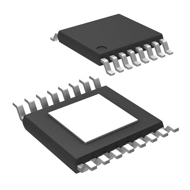
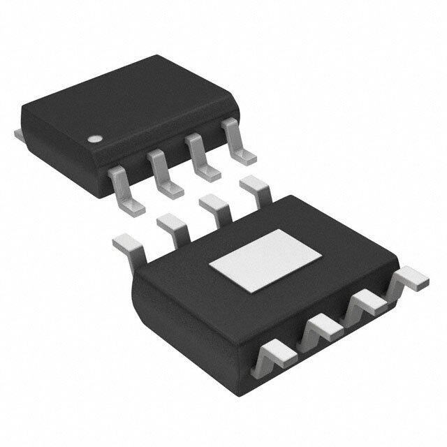
| 产品图片 |
|
| rohs | 符合RoHS无铅 / 符合限制有害物质指令(RoHS)规范要求 |
| 产品系列 | 电源管理 IC,稳压器—开关式稳压器,Texas Instruments LM2651MTCX-3.3/NOPB- |
| 数据手册 | |
| 产品型号 | LM2651MTCX-3.3/NOPB |
| PWM类型 | 电流模式 |
| 产品种类 | 稳压器—开关式稳压器 |
| 供应商器件封装 | 16-TSSOP |
| 其它名称 | *LM2651MTCX-3.3/NOPB |
| 包装 | 带卷 (TR) |
| 同步整流器 | 是 |
| 商标 | Texas Instruments |
| 安装类型 | 表面贴装 |
| 安装风格 | SMD/SMT |
| 封装 | Reel |
| 封装/外壳 | 16-TSSOP(0.173",4.40mm 宽) |
| 封装/箱体 | TSSOP-16 |
| 工作温度 | -40°C ~ 125°C |
| 工厂包装数量 | 2500 |
| 开关频率 | 330 kHz |
| 最大工作温度 | + 125 C |
| 最大输入电压 | 14 V |
| 最小工作温度 | - 40 C |
| 最小输入电压 | 4 V |
| 标准包装 | 2,500 |
| 电压-输入 | 4 V ~ 14 V |
| 电压-输出 | 3.3V |
| 电流-输出 | 1.5A |
| 类型 | Step Down |
| 系列 | LM2651 |
| 设计资源 | http://www.digikey.com/product-highlights/cn/zh/texas-instruments-webench-design-center/3176 |
| 负载调节 | 1.3 % |
| 输出数 | 1 |
| 输出电压 | 3.3 V |
| 输出电流 | 1.5 A |
| 输出端数量 | 1 Output |
| 输出类型 | 固定 |
| 配用 | /product-detail/zh/LM2651EVAL/LM2651EVAL-ND/366866/product-detail/zh/LM2651-3.3EVAL/LM2651-3.3EVAL-ND/366865 |
| 频率-开关 | 300kHz |




- 商务部:美国ITC正式对集成电路等产品启动337调查
- 曝三星4nm工艺存在良率问题 高通将骁龙8 Gen1或转产台积电
- 太阳诱电将投资9.5亿元在常州建新厂生产MLCC 预计2023年完工
- 英特尔发布欧洲新工厂建设计划 深化IDM 2.0 战略
- 台积电先进制程称霸业界 有大客户加持明年业绩稳了
- 达到5530亿美元!SIA预计今年全球半导体销售额将创下新高
- 英特尔拟将自动驾驶子公司Mobileye上市 估值或超500亿美元
- 三星加码芯片和SET,合并消费电子和移动部门,撤换高东真等 CEO
- 三星电子宣布重大人事变动 还合并消费电子和移动部门
- 海关总署:前11个月进口集成电路产品价值2.52万亿元 增长14.8%



PDF Datasheet 数据手册内容提取
Product Sample & Technical Tools & Support & Folder Buy Documents Software Community LM2651 SNVS032E–FEBRUARY2000–REVISEDJANUARY2016 LM2651 1.5 A High-Efficiency Synchronous Switching Regulator 1 Features 3 Description • UltrahighEfficiencyupto97% The LM2651 switching regulator provides high- 1 efficiency power conversion over a 100:1 load range • High-EfficiencyOvera1.5-Ato1.5-mALoad (1.5 A to 15 mA). This feature makes the LM2651 an Range ideal fit in battery-powered applications that demand • 4-Vto14-VInputVoltageRange longbatterylifeinbothrunandstandbymodes. • 1.8-V,2.5-V,3.3-V,orADJOutputVoltage Synchronous rectification is used to achieve up to • InternalMOSFETSwitchWithLowR of 97% efficiency. At light loads, the LM2651 enters a DS(on) 75mΩ low power hysteretic or sleep mode to maintain high efficiency. In many applications, the efficiency still • 300-kHzFixedFrequencyInternalOscillator exceeds 80% at 15-mA load. A shutdown pin is • 7-µAShutdownCurrent available to disable the LM2651 and reduce the • PatentedCurrentSensingforCurrentMode supplycurrenttolessthan10 µA. Control The LM2651 contains a patented current sensing • InputUndervoltageLockout circuitry for current mode control. This feature • AdjustableSoft-Start eliminates the external current sensing resistor requiredbyothercurrent-modeDC-DCconverters. • CurrentLimitandThermalShutdown • 16-PinTSSOPPackage The LM2651 has a 300-kHz fixed frequency internal oscillator. The high oscillator frequency allows the 2 Applications useofextremelysmall,low-profilecomponents. • PersonalDigitalAssistants(PDAs) A programmable soft-start feature limits current surges from the input power supply at start-up and • ComputerPeripherals provides a simple means of sequencing multiple • Battery-PoweredDevices powersupplies. • HandheldScanners Other protection features include input undervoltage • High-Efficiency5-VConversion lockout,currentlimiting,andthermalshutdown. DeviceInformation(1) PARTNUMBER PACKAGE BODYSIZE(NOM) LM2651 TSSOP(16) 5.00mm×4.40mm (1) For all available packages, see the orderable addendum at theendofthedatasheet. TypicalApplication 1 An IMPORTANT NOTICE at the end of this data sheet addresses availability, warranty, changes, use in safety-critical applications, intellectualpropertymattersandotherimportantdisclaimers.PRODUCTIONDATA.
LM2651 SNVS032E–FEBRUARY2000–REVISEDJANUARY2016 www.ti.com Table of Contents 1 Features.................................................................. 1 7.3 FeatureDescription.................................................11 2 Applications........................................................... 1 7.4 DeviceFunctionalModes........................................11 3 Description............................................................. 1 8 ApplicationandImplementation........................ 12 4 RevisionHistory..................................................... 2 8.1 ApplicationInformation............................................12 8.2 TypicalApplication..................................................12 5 PinConfigurationandFunctions......................... 3 9 PowerSupplyRecommendations...................... 16 6 Specifications......................................................... 4 10 Layout................................................................... 16 6.1 AbsoluteMaximumRatings......................................4 6.2 ESDRatings..............................................................4 10.1 LayoutGuidelines.................................................16 6.3 RecommendedOperatingConditions.......................4 10.2 LayoutExample....................................................16 6.4 ThermalInformation .................................................4 11 DeviceandDocumentationSupport................. 17 6.5 ElectricalCharacteristics...........................................5 11.1 CommunityResources..........................................17 6.6 TypicalCharacteristics..............................................8 11.2 Trademarks...........................................................17 7 DetailedDescription............................................ 10 11.3 ElectrostaticDischargeCaution............................17 7.1 Overview.................................................................10 11.4 Glossary................................................................17 7.2 FunctionalBlockDiagram.......................................10 12 Mechanical,Packaging,andOrderable Information........................................................... 17 4 Revision History ChangesfromRevisionD(April2013)toRevisionE Page • AddedESDRatingstable,ThermalInformationtable,FeatureDescriptionsection,DeviceFunctionalModes, ApplicationandImplementationsection,PowerSupplyRecommendationssection,Layoutsection,Deviceand DocumentationSupportsection,andMechanical,Packaging,andOrderableInformationsection ..................................... 1 2 SubmitDocumentationFeedback Copyright©2000–2016,TexasInstrumentsIncorporated ProductFolderLinks:LM2651
LM2651 www.ti.com SNVS032E–FEBRUARY2000–REVISEDJANUARY2016 5 Pin Configuration and Functions PWPackage 16-PinTSSOP TopView PinFunctions PIN TYPE(1) DESCRIPTION NO. NAME 1,2 SW O Switched-nodeconnection,whichisconnectedwiththesourceoftheinternalhigh-sideMOSFET. 3to5 VIN I Mainpowersupplypin 6 VCB I Bootstrapcapacitorconnectionforhigh-sidegatedrive 7 AVIN I Inputsupplyvoltageforcontrolanddrivercircuits Shutdownandsoft-startcontrolpin.Pullingthispinbelow0.3Vshutsofftheregulator.Acapacitor 8 SD(SS) I connectedfromthispintogroundprovidesacontrolrampoftheinputcurrent.Donotdrivethispin withanexternalsourceorerroneousoperationmayresult. 9 FB I Outputvoltagefeedbackinput.Connectedtotheoutputvoltage. 10 COMP I Compensationnetworkconnection.Connectedtotheoutputofthevoltageerroramplifier. 11 NC G Nointernalconnection 12to13 AGND G Low-noiseanalogground 14to16 PGND G Powerground (1) I=Input,O=Output,andG=Ground Copyright©2000–2016,TexasInstrumentsIncorporated SubmitDocumentationFeedback 3 ProductFolderLinks:LM2651
LM2651 SNVS032E–FEBRUARY2000–REVISEDJANUARY2016 www.ti.com 6 Specifications 6.1 Absolute Maximum Ratings overoperatingfree-airtemperaturerange(unlessotherwisenoted)(1)(2) MIN MAX UNIT Inputvoltage 15 V Feedbackpinvoltage −0.4 5 V Powerdissipation(T =25°C)(3) 893 mW A Junctiontemperature,T −40 125 °C J Storagetemperature,T −65 150 °C stg (1) StressesbeyondthoselistedunderAbsoluteMaximumRatingsmaycausepermanentdamagetothedevice.Thesearestressratings only,whichdonotimplyfunctionaloperationofthedeviceattheseoranyotherconditionsbeyondthoseindicatedunderRecommended OperatingConditions.Exposuretoabsolute-maximum-ratedconditionsforextendedperiodsmayaffectdevicereliability. (2) IfMilitary/Aerospacespecifieddevicesarerequired,pleasecontacttheTISalesOffice/Distributorsforavailabilityandspecifications. (3) ThemaximumallowablepowerdissipationiscalculatedbyusingP =(T –T )/θ ,whereT isthemaximumjunction Dmax Jmax A JA Jmax temperature,T istheambienttemperature,andθ isthejunction-to-ambientthermalresistanceofthespecifiedpackage.The893- A JA mWratingresultsfromusing150°C,25°C,and140°C/WforT ,T ,andθ respectively.Aθ of140°C/Wrepresentstheworst- Jmax A JA JA caseconditionofnoheatsinkingofthe16-pinTSSOPpackage.Heatsinkingallowsthesafedissipationofmorepower.Theabsolute maximumpowerdissipationmustbederatedby7.14mWper°Cabove25°Cambient.TheLM2651activelylimitsitsjunction temperaturetoabout165°C. 6.2 ESD Ratings VALUE UNIT V Electrostaticdischarge Human-bodymodel(HBM),perANSI/ESDA/JEDECJS-001(1) ±1000 V (ESD) (1) JEDECdocumentJEP155statesthat500-VHBMallowssafemanufacturingwithastandardESDcontrolprocess. 6.3 Recommended Operating Conditions overoperatingfree-airtemperaturerange(unlessotherwisenoted) MIN NOM MAX UNIT V Supplyvoltage 4 14 V IN 6.4 Thermal Information LM2651 THERMALMETRIC(1) PW(TSSOP) UNIT 16PINS R Junction-to-ambientthermalresistance 97.3 °C/W θJA R Junction-to-case(top)thermalresistance 29.9 °C/W θJC(top) R Junction-to-boardthermalresistance 43.1 °C/W θJB ψ Junction-to-topcharacterizationparameter 1.8 °C/W JT ψ Junction-to-boardcharacterizationparameter 42.4 °C/W JB R Junction-to-case(bottom)thermalresistance — °C/W θJC(bot) (1) Formoreinformationabouttraditionalandnewthermalmetrics,seetheSemiconductorandICPackageThermalMetricsapplication report,SPRA953. 4 SubmitDocumentationFeedback Copyright©2000–2016,TexasInstrumentsIncorporated ProductFolderLinks:LM2651
LM2651 www.ti.com SNVS032E–FEBRUARY2000–REVISEDJANUARY2016 6.5 Electrical Characteristics specificationsareT =25°CandV =10V(unlessotherwisespecified)(1) J IN PARAMETER TESTCONDITIONS MIN TYP(2) MAX UNIT LM2651-1.8 T =25°C 1.761 1.8 1.836 J Outputvoltage I =900mA Overfulloperating V LOAD junctiontemperature 1.719 1.854 range V OUT Outputvoltagelineregulation V =4Vto14V,I =900mA 0.2% IN LOAD I =10mAto1.5A,V =5V 1.3% LOAD IN Outputvoltageloadregulation I =200mAto1.5A,V =5V 0.3% LOAD IN Sleepmodeoutputvoltage V 35 mV HYST hysteresis LM2651-2.5 T =25°C 2.43 2.5 2.574 J Outputvoltage I =900mA Overfulloperating V LOAD junctiontemperature 2.388 2.575 range V OUT Outputvoltagelineregulation V =4Vto12V,I =900mA 0.2% IN LOAD I =10mAto1.5A,V =5V 1.3% LOAD IN Outputvoltageloadregulation I =200mAto1.5A,V =5V 0.3% LOAD IN Sleepmodeoutputvoltage V 48 mV HYST hysteresis LM2651-3.3 T =25°C 3.265 3.3 3.379 J Outputvoltage I =900mA Overfulloperating V LOAD junctiontemperature 3.201 3.399 range V OUT Outputvoltagelineregulation V =4Vto14V,I =900mA 0.2% IN LOAD I =10mAto1.5A,V =5V 1.3% LOAD IN Outputvoltageloadregulation I =200mAto1.5A,V =5V 0.3% LOAD IN Sleepmodeoutputvoltage V 60 mV HYST hysteresis LM2651-ADJ(3) T =25°C 1.238 J V Feedbackvoltage I =900mA Overfulloperating V FB LOAD junctiontemperature 1.2 1.263 range Outputvoltagelineregulation V =4Vto14V,I =900mA 0.2% IN LOAD V I =10mAto1.5A,V =5V 1.3% OUT LOAD IN Outputvoltageloadregulation I =200mAto1.5A,V =5V 0.3% LOAD IN Sleepmodeoutputvoltage V 24 mV HYST hysteresis ALLOUTPUTVOLTAGEVERSIONS T =25°C 1.6 J I Quiescentcurrent mA Q Overfulloperatingjunctiontemperaturerange 2 T =25°C 7 12 J I Quiescentcurrentinshutdown Shutdownpinpulled Overfulloperating µA QSD mode low junctiontemperature 20 range (1) Alllimitsareensuredatroomtemperature(standardtypeface)andattemperatureextremes.Allroomtemperaturelimitsare100% productiontested.AlllimitsattemperatureextremesarespecifiedviacorrelationusingstandardStatisticalQualityControl(SQC) methods.AlllimitsareusedtocalculateAverageOutgoingQualityLevel(AOQL). (2) Typicalnumbersareat25°Candrepresentthemostlikelynorm. (3) V =2.5V OUT Copyright©2000–2016,TexasInstrumentsIncorporated SubmitDocumentationFeedback 5 ProductFolderLinks:LM2651
LM2651 SNVS032E–FEBRUARY2000–REVISEDJANUARY2016 www.ti.com Electrical Characteristics (continued) specificationsareT =25°CandV =10V(unlessotherwisespecified)(1) J IN PARAMETER TESTCONDITIONS MIN TYP(2) MAX UNIT High-Sideorlow-sideswitchon resistance(MOSFETon R I =1A 110 mΩ SW(ON) resistance+bondingwire SWITCH resistance) T =25°C 75 J R MOSFETonresistance(high- I =1A Overfulloperating mΩ DS(ON) sideorlow-side) SWITCH junctiontemperature 130 range Switchleakagecurrent-high 130 side I nA L Switchleakagecurrent-low 130 side T =25°C 6.45 6.75 6.95 J V Bootstrapregulatorvoltage I =1mA Overfulloperating V BOOT BOOT junctiontemperature 6.4 7 range G Erroramplifiertransconductance 1250 µmho M T =25°C 3.8 J V VINundervoltagelockout Risingedge Overfulloperating V INUV thresholdvoltage junctiontemperature 3.95 range Hysteresisfortheundervoltage V 210 mV UV-HYST lockout T =25°C 2 J I Switchcurrentlimit V =5V Overfulloperating A CL IN junctiontemperature 1.55 2.6 range I Sleepmodethresholdcurrent V =5V 100 mA SM IN A Erroramplifiervoltagegain 100 V/V V T =25°C 25 40 J I Erroramplifiersourcecurrent µA EA_SOURCE Overfulloperatingjunctiontemperaturerange 15 T =25°C 65 J I Erroramplifiersinkcurrent µA EA_SINK Overfulloperatingjunctiontemperaturerange 30 Erroramplifieroutputswing TJ=25°C 2.5 2.7 V V EAH upperlimit Overfulloperatingjunctiontemperaturerange 2.4 Erroramplifieroutputswing TJ=25°C 1.25 1.35 V V EAL lowerlimit Overfulloperatingjunctiontemperaturerange 1.5 V Bodydiodevoltage I =1.5A 1 V D DIODE T =25°C 280 300 330 J f Oscillatorfrequency V =4V Overfulloperating kHz OSC IN junctiontemperature 255 345 range T =25°C 95% J D Maximumdutycycle V =4V Overfulloperating MAX IN junctiontemperature 92% range T =25°C 11 J I Soft-Startcurrent VoltageattheSSpin Overfulloperating µA SS =1.4V junctiontemperature 7 14 range 6 SubmitDocumentationFeedback Copyright©2000–2016,TexasInstrumentsIncorporated ProductFolderLinks:LM2651
LM2651 www.ti.com SNVS032E–FEBRUARY2000–REVISEDJANUARY2016 Electrical Characteristics (continued) specificationsareT =25°CandV =10V(unlessotherwisespecified)(1) J IN PARAMETER TESTCONDITIONS MIN TYP(2) MAX UNIT T =25°C 0.8 2.2 3.7 J I Shutdownpincurrent Shutdownpinpulled Overfulloperating µA SHUTDOWN low junctiontemperature 0.5 4 range T =25°C 0.6 J v Shutdownpinthresholdvoltage Fallingedge Overfulloperating V SHUTDOWN junctiontemperature 0.3 0.9 range T Thermalshutdowntemperature 165 °C SD Thermalshutdownhysteresis T 25 °C SD_HYST temperature Copyright©2000–2016,TexasInstrumentsIncorporated SubmitDocumentationFeedback 7 ProductFolderLinks:LM2651
LM2651 SNVS032E–FEBRUARY2000–REVISEDJANUARY2016 www.ti.com 6.6 Typical Characteristics Figure1.I vsInputVoltage Figure2.I vsInputVoltage Q QSD Figure3.I vsJunctionTemperature Figure4.FrequencyvsJunctionTemperature QSD Figure5.RDS(ON)vsInputVoltage Figure6.RDS(ON)vsJunctionTemperature 8 SubmitDocumentationFeedback Copyright©2000–2016,TexasInstrumentsIncorporated ProductFolderLinks:LM2651
LM2651 www.ti.com SNVS032E–FEBRUARY2000–REVISEDJANUARY2016 Typical Characteristics (continued) Figure7.CurrentLimitvsInputVoltage Figure8.CurrentLimitvsJunctionTemperature (VOUT=2.5V) (VOUT=2.5V) Figure9.CurrentLimitvsJunctionTemperature Figure10.CurrentLimitvsInputVoltage (V =3.3V) (V =3.3V) OUT OUT Copyright©2000–2016,TexasInstrumentsIncorporated SubmitDocumentationFeedback 9 ProductFolderLinks:LM2651
LM2651 SNVS032E–FEBRUARY2000–REVISEDJANUARY2016 www.ti.com 7 Detailed Description 7.1 Overview The LM2651 operates in a constant frequency (300 kHz), current-mode PWM for moderate to heavy loads, and automatically switches to hysteretic mode for light loads. In hysteretic mode, the switching frequency is reduced tomaintainhighefficiency. 7.2 Functional Block Diagram 10 SubmitDocumentationFeedback Copyright©2000–2016,TexasInstrumentsIncorporated ProductFolderLinks:LM2651
LM2651 www.ti.com SNVS032E–FEBRUARY2000–REVISEDJANUARY2016 7.3 Feature Description When the load current is higher than the sleep mode threshold, the part is always operating in PWM mode. At the beginning of each switching cycle, the high-side switch is turned on, the current from the high-side switch is sensed and compared with the output of the error amplifier (COMP pin). When the sensed current reaches the COMP pin voltage level, the high-side switch is turned off; after 40 ns (deadtime), the low-side switch is turned on.Attheendoftheswitchingcycle,thelow-sideswitchisturnedoff;andthesamecyclerepeats. When the load current decreases below the sleep mode threshold, the output voltage rises slightly, this rise is sensed by the hysteretic mode comparator which makes the part go into the hysteretic mode with both the high and low side switches off. The output voltage starts to drop until it hits the low threshold of the hysteretic comparator, and the part immediately goes back to the PWM operation. The output voltage keeps increasing until it reaches the top hysteretic threshold, then both the high- and low-side switches turn off again, and the cyclerepeats. 7.4 Device Functional Modes The cycle-by-cycle current limit circuitry turns off the high-side MOSFET whenever the current in MOSFET reaches2A.AshutdownpinisavailabletodisabletheLM2651andreducethesupplycurrentto7µA. Copyright©2000–2016,TexasInstrumentsIncorporated SubmitDocumentationFeedback 11 ProductFolderLinks:LM2651
LM2651 SNVS032E–FEBRUARY2000–REVISEDJANUARY2016 www.ti.com 8 Application and Implementation NOTE Information in the following applications sections is not part of the TI component specification, and TI does not warrant its accuracy or completeness. TI’s customers are responsible for determining suitability of components for their purposes. Customers should validateandtesttheirdesignimplementationtoconfirmsystemfunctionality. 8.1 Application Information LM2651 operates in a constant frequency (300 kHz), current-mode PWM for moderate to heavy loads; and it automatically switches to hysteretic mode for light loads. The current of the top switch is sensed by a patented internal circuitry. This unique technique gets rid of the external sense resistor, saves cost and size, and improves noise immunity of the sensed current. A feed forward from the input voltage is added to reduce the variation of thecurrentlimitovertheinputvoltagerange. 8.2 Typical Application Figure11. SchematicfortheTypicalBoardLayout 8.2.1 DesignRequirements To properly size the components for the application, the designer needs the following parameters: input voltage range, output voltage, output current range, and the switching frequency. These four main parameters affect the choices of component available to achieve a proper system behavior. TI recommends a Schottky diode to prevent the intrinsic body diode of the low-side MOSFET from conducting during deadtime. See Detailed Design Procedureformoreinformation. 8.2.2 DetailedDesignProcedure Thissectionpresentsguidelinesforselectingexternalcomponents. 8.2.2.1 InputCapacitor A low ESR aluminum, tantalum, or ceramic capacitor is needed between the input pin and power ground. This capacitor prevents large voltage transients from appearing at the input. The capacitor is selected based on the RMScurrentandvoltagerequirements.TheRMScurrentisgivenbyEquation1. V (V -V ) I =I ´ OUT IN OUT RMS OUT V IN (1) 12 SubmitDocumentationFeedback Copyright©2000–2016,TexasInstrumentsIncorporated ProductFolderLinks:LM2651
LM2651 www.ti.com SNVS032E–FEBRUARY2000–REVISEDJANUARY2016 Typical Application (continued) The RMS current reaches its maximum (I /2) when V equals 2 V . For an aluminum or ceramic capacitor, OUT IN OUT the voltage rating should be at least 25% higher than the maximum input voltage. If a tantalum capacitor is used, the voltage rating required is about twice the maximum input voltage. The tantalum capacitor should be surge- current tested by the manufacturer to prevent being shorted by the inrush current. TI also recommends putting a smallceramiccapacitor(0.1μF)betweentheinputpinandgroundpintoreducehigh-frequencyspikes. 8.2.2.2 Inductor The most critical parameters for the inductor are the inductance, peak current, and the DC resistance. The inductance is related to the peak-to-peak inductor ripple current, the input and the output voltages, as given by Equation2. (V -V )V L = IN OUT OUT V ´I ´300kHz IN RIPPLE (2) Ahighervalueofripplecurrentreducesinductance,butincreasestheconductanceloss,coreloss,currentstress for the inductor and switch devices. It also requires a bigger output capacitor for the same output voltage ripple requirement. A reasonable value is setting the ripple current to be 30% of the DC output current. Since the ripple current increases with the input voltage, the maximum input voltage is always used to determine the inductance. The DC resistance of the inductor is a key parameter for the efficiency. Lower DC resistance is available with a bigger winding area. A good tradeoff between the efficiency and the core size is letting the inductor copper loss equal2%oftheoutputpower. 8.2.2.3 OutputCapacitor The selection of C is driven by the maximum allowable output voltage ripple. The output ripple in the constant OUT frequency,PWMmodeisapproximatedbyusingEquation3. æ 1 ö V =I çESR+ ÷ RIPPLE RIPPLE 8F C è S OUT ø (3) The ESR term usually plays the dominant role in determining the voltage ripple. A low ESR aluminum electrolytic or tantalum capacitor (such as Nichicon PL series, Sanyo OS-CON, Sprague 593D, 594D, AVX TPS, and CDE polymer aluminum) is recommended. An electrolytic capacitor is not recommended for temperatures below −25°C since its ESR rises dramatically at cold temperature. A tantalum capacitor has a much better ESR specificationatcoldtemperatureandispreferredforlowtemperatureapplications. The output voltage ripple in constant frequency mode has to be less than the sleep mode voltage hysteresis to avoidenteringthesleepmodeatfullloadasgivenbyEquation4. V <20mVxV /V (4) RIPPLE OUT FB 8.2.2.4 BoostCapacitor TI recommends a 0.1-μF ceramic capacitor for the boost capacitor. The typical voltage across the boost capacitoris6.7V. 8.2.2.5 Soft-StartCapacitor A soft-start capacitor is used to provide the soft-start feature. When the input voltage is first applied, or when the SD(SS) pin is allowed to go high, the soft-start capacitor is charged by a current source (approximately 2 μA). When the SD(SS) pin voltage reaches 0.6 V (shutdown threshold), the internal regulator circuitry starts to operate. The current charging the soft-start capacitor increases from 2 μA to approximately 10 μA. With the SD(SS) pin voltage between 0.6 V and 1.3 V, the level of the current limit is zero, which means the output voltage is still zero. When the SD(SS) pin voltage increases beyond 1.3 V, the current limit starts to increase. The switch duty cycle, which is controlled by the level of the current limit, starts with narrow pulses and gradually gets wider. At the same time, the output voltage of the converter increases towards the nominal value, which brings down the output voltage of the error amplifier. When the output of the error amplifier is less than the current limit voltage, it takes over the control of the duty cycle. The converter enters the normal current-mode PWMoperation.The SD(SS)pinvoltageiseventuallychargeduptoabout2V. Copyright©2000–2016,TexasInstrumentsIncorporated SubmitDocumentationFeedback 13 ProductFolderLinks:LM2651
LM2651 SNVS032E–FEBRUARY2000–REVISEDJANUARY2016 www.ti.com Typical Application (continued) Thesoft-starttimecanbeestimatedusingEquation5. T =C x0.6V/2μA+C x(2V−0.6V)/10μA (5) SS SS SS 8.2.2.6 R andR (ProgrammingOutputVoltage) 1 2 UseEquation6toselecttheappropriateresistorvalues. V =V (1+R /R ) OUT REF 1 2 where • V =1.238V (6) REF Selectresistorsbetween10kΩ and100kΩ.(1%orhigheraccuracymetalfilmresistorsforR andR .) 1 2 8.2.2.7 CompensationComponents In the control to output transfer function, the first pole F can be estimated as 1/(2πR C ); The ESR zero p1 OUT OUT F of the output capacitor is 1/(2πESRC ); Also, there is a high-frequency pole F in the range of 45 kHz to z1 OUT p2 150kHzasgivenbyEquation7. F =F/(πn(1−D)) p2 s where • D=V /V OUT IN • n=1+0.348L/(V −V )(LisinµHsandV andV involts). (7) IN OUT IN OUT ThetotalloopgainGisapproximately500/I whereI isinamperes. OUT OUT AGmamplifierisusedinsidetheLM2651.TheoutputresistorR oftheGmamplifierisabout80kΩ.C andR o c1 C togetherwithR givealagcompensationtorolloffthegainasgivenbyEquation8. o F =1/(2πC (R +R)),F =1/2πC R. (8) pc1 c1 o c zc1 c1 c In some applications, the ESR zero F cannot be cancelled by F . Then, C is needed to introduce F to z1 p2 c2 pc2 canceltheESRzero,F =1/(2πC R ‖R ). p2 c2 o c Theruleofthumbistohavemorethan45° phasemarginatthecrossoverfrequency(G=1). If C is higher than 68 µF, C = 2.2 nF, and R = 15 kΩ are good choices for most applications. If the ESR OUT c1 c zeroistoolowtobecancelledbyF ,addC . p2 c2 Ifthetransientresponsetoasteploadisimportant,chooseR tobehigherthan10kΩ. C 8.2.2.8 ExternalSchottkyDiode TI recommends a Schottky diode D to prevent the intrinsic body diode of the low-side MOSFET from conducting 1 during the deadtime in PWM operation and hysteretic mode when both MOSFETs are off. If the body diode turns on,thereisextrapowerdissipationinthebodydiodebecauseofthereverse-recoverycurrentandhigherforward voltage; the high-side MOSFET also has more switching loss since the negative diode reverse-recovery current appears as the high-side MOSFET turnon current in addition to the load current. These losses degrade the efficiency by 1–2%. The improved efficiency and noise immunity with the Schottky diode become more obvious withincreasinginputvoltageandloadcurrent. The breakdown voltage rating of D is preferred to be 25% higher than the maximum input voltage. Since D is 1 1 only on for a short period of time, the average current rating for D only requires being higher than 30% of the 1 maximum output current. It is important to place D very close to the drain and source of the low-side MOSFET, 1 extra parasitic inductance in the parallel loop slows the turnon of D and direct the current through the body 1 diodeofthelow-sideMOSFET. When an undervoltage situation occurs, the output voltage can be pulled below ground as the inductor current is reversed through the synchronous FET. For applications that require protection from a negative voltage, TI recommends a clamping diode D2. When used, D2 should be connected cathode to V and anode to ground. OUT TIrecommendsadioderatedforaminimumof2A. 14 SubmitDocumentationFeedback Copyright©2000–2016,TexasInstrumentsIncorporated ProductFolderLinks:LM2651
LM2651 www.ti.com SNVS032E–FEBRUARY2000–REVISEDJANUARY2016 Typical Application (continued) 8.2.3 ApplicationCurves (V =5V,V =3.3V) IN OUT Figure12.EfficiencyvsLoadCurrent Figure13.SleepModeThresholdvsOutputVoltage ForADJVersion(V =5V) IN Copyright©2000–2016,TexasInstrumentsIncorporated SubmitDocumentationFeedback 15 ProductFolderLinks:LM2651
LM2651 SNVS032E–FEBRUARY2000–REVISEDJANUARY2016 www.ti.com 9 Power Supply Recommendations The LM2651 is designed to operate from various DC power supplies. If so, VIN input should be protected from reversal voltage and voltage dump over 15 V. The impedance of the input supply rail should be low enough that the input current transient does not cause drop below VIN UVLO level. If the input supply is connected by using longwires,additionalbulkcapacitancemayberequiredinadditiontonormalinputcapacitor. 10 Layout 10.1 Layout Guidelines Layout is critical to reduce noises and ensure specified performance. The important guidelines are listed as follows: 1. MinimizetheparasiticinductanceintheloopofinputcapacitorsandtheinternalMOSFETsbyconnectingthe input capacitors to V and PGND pins with short and wide traces. This is important because the rapidly IN switching current, together with wiring inductance can generate large voltage spikes that may result in noise problems. 2. Minimize the trace from the center of the output resistor divider to the FB pin and keep it away from noise sources to avoid noise pickup. For applications requiring tight regulation at the output, TI recommends a dedicated sense trace (separated from the power trace) to connect the top of the resistor divider to the output. 3. IftheSchottkydiodeD isused,minimizethetracesconnectingD toSWandPGNDpins. 1 1 10.2 Layout Example Figure14. LM2651LayoutRecommendation 16 SubmitDocumentationFeedback Copyright©2000–2016,TexasInstrumentsIncorporated ProductFolderLinks:LM2651
LM2651 www.ti.com SNVS032E–FEBRUARY2000–REVISEDJANUARY2016 11 Device and Documentation Support 11.1 Community Resources The following links connect to TI community resources. Linked contents are provided "AS IS" by the respective contributors. They do not constitute TI specifications and do not necessarily reflect TI's views; see TI's Terms of Use. TIE2E™OnlineCommunity TI'sEngineer-to-Engineer(E2E)Community.Createdtofostercollaboration amongengineers.Ate2e.ti.com,youcanaskquestions,shareknowledge,exploreideasandhelp solveproblemswithfellowengineers. DesignSupport TI'sDesignSupport QuicklyfindhelpfulE2Eforumsalongwithdesignsupporttoolsand contactinformationfortechnicalsupport. 11.2 Trademarks E2EisatrademarkofTexasInstruments. Allothertrademarksarethepropertyoftheirrespectiveowners. 11.3 Electrostatic Discharge Caution Thesedeviceshavelimitedbuilt-inESDprotection.Theleadsshouldbeshortedtogetherorthedeviceplacedinconductivefoam duringstorageorhandlingtopreventelectrostaticdamagetotheMOSgates. 11.4 Glossary SLYZ022—TIGlossary. Thisglossarylistsandexplainsterms,acronyms,anddefinitions. 12 Mechanical, Packaging, and Orderable Information The following pages include mechanical, packaging, and orderable information. This information is the most current data available for the designated devices. This data is subject to change without notice and revision of thisdocument.Forbrowser-basedversionsofthisdatasheet,refertotheleft-handnavigation. Copyright©2000–2016,TexasInstrumentsIncorporated SubmitDocumentationFeedback 17 ProductFolderLinks:LM2651
PACKAGE OPTION ADDENDUM www.ti.com 6-Feb-2020 PACKAGING INFORMATION Orderable Device Status Package Type Package Pins Package Eco Plan Lead/Ball Finish MSL Peak Temp Op Temp (°C) Device Marking Samples (1) Drawing Qty (2) (6) (3) (4/5) LM2651MTC-3.3/NOPB ACTIVE TSSOP PW 16 92 Green (RoHS SN Level-1-260C-UNLIM -40 to 125 2651MTC & no Sb/Br) -3.3 LM2651MTC-ADJ NRND TSSOP PW 16 92 TBD Call TI Call TI -40 to 125 2651MTC -ADJ LM2651MTC-ADJ/NOPB ACTIVE TSSOP PW 16 92 Green (RoHS SN Level-1-260C-UNLIM -40 to 125 2651MTC & no Sb/Br) -ADJ LM2651MTCX-3.3/NOPB ACTIVE TSSOP PW 16 2500 Green (RoHS SN Level-1-260C-UNLIM -40 to 125 2651MTC & no Sb/Br) -3.3 LM2651MTCX-ADJ/NOPB ACTIVE TSSOP PW 16 2500 Green (RoHS SN Level-1-260C-UNLIM -40 to 125 2651MTC & no Sb/Br) -ADJ (1) The marketing status values are defined as follows: ACTIVE: Product device recommended for new designs. LIFEBUY: TI has announced that the device will be discontinued, and a lifetime-buy period is in effect. NRND: Not recommended for new designs. Device is in production to support existing customers, but TI does not recommend using this part in a new design. PREVIEW: Device has been announced but is not in production. Samples may or may not be available. OBSOLETE: TI has discontinued the production of the device. (2) RoHS: TI defines "RoHS" to mean semiconductor products that are compliant with the current EU RoHS requirements for all 10 RoHS substances, including the requirement that RoHS substance do not exceed 0.1% by weight in homogeneous materials. Where designed to be soldered at high temperatures, "RoHS" products are suitable for use in specified lead-free processes. TI may reference these types of products as "Pb-Free". RoHS Exempt: TI defines "RoHS Exempt" to mean products that contain lead but are compliant with EU RoHS pursuant to a specific EU RoHS exemption. Green: TI defines "Green" to mean the content of Chlorine (Cl) and Bromine (Br) based flame retardants meet JS709B low halogen requirements of <=1000ppm threshold. Antimony trioxide based flame retardants must also meet the <=1000ppm threshold requirement. (3) MSL, Peak Temp. - The Moisture Sensitivity Level rating according to the JEDEC industry standard classifications, and peak solder temperature. (4) There may be additional marking, which relates to the logo, the lot trace code information, or the environmental category on the device. (5) Multiple Device Markings will be inside parentheses. Only one Device Marking contained in parentheses and separated by a "~" will appear on a device. If a line is indented then it is a continuation of the previous line and the two combined represent the entire Device Marking for that device. (6) Lead/Ball Finish - Orderable Devices may have multiple material finish options. Finish options are separated by a vertical ruled line. Lead/Ball Finish values may wrap to two lines if the finish value exceeds the maximum column width. Addendum-Page 1
PACKAGE OPTION ADDENDUM www.ti.com 6-Feb-2020 Important Information and Disclaimer:The information provided on this page represents TI's knowledge and belief as of the date that it is provided. TI bases its knowledge and belief on information provided by third parties, and makes no representation or warranty as to the accuracy of such information. Efforts are underway to better integrate information from third parties. TI has taken and continues to take reasonable steps to provide representative and accurate information but may not have conducted destructive testing or chemical analysis on incoming materials and chemicals. TI and TI suppliers consider certain information to be proprietary, and thus CAS numbers and other limited information may not be available for release. In no event shall TI's liability arising out of such information exceed the total purchase price of the TI part(s) at issue in this document sold by TI to Customer on an annual basis. Addendum-Page 2
PACKAGE MATERIALS INFORMATION www.ti.com 6-Nov-2015 TAPE AND REEL INFORMATION *Alldimensionsarenominal Device Package Package Pins SPQ Reel Reel A0 B0 K0 P1 W Pin1 Type Drawing Diameter Width (mm) (mm) (mm) (mm) (mm) Quadrant (mm) W1(mm) LM2651MTCX-3.3/NOPB TSSOP PW 16 2500 330.0 12.4 6.95 5.6 1.6 8.0 12.0 Q1 LM2651MTCX-ADJ/NOPB TSSOP PW 16 2500 330.0 12.4 6.95 5.6 1.6 8.0 12.0 Q1 PackMaterials-Page1
PACKAGE MATERIALS INFORMATION www.ti.com 6-Nov-2015 *Alldimensionsarenominal Device PackageType PackageDrawing Pins SPQ Length(mm) Width(mm) Height(mm) LM2651MTCX-3.3/NOPB TSSOP PW 16 2500 367.0 367.0 35.0 LM2651MTCX-ADJ/NOPB TSSOP PW 16 2500 367.0 367.0 35.0 PackMaterials-Page2
PACKAGE OUTLINE PW0016A TSSOP - 1.2 mm max height SCALE 2.500 SMALL OUTLINE PACKAGE SEATING PLANE C 6.6 TYP 6.2 A 0.1 C PIN 1 INDEX AREA 14X 0.65 16 1 2X 5.1 4.55 4.9 NOTE 3 8 9 0.30 B 4.5 16X 0.19 1.2 MAX 4.3 0.1 C A B NOTE 4 (0.15) TYP SEE DETAIL A 0.25 GAGE PLANE 0.15 0.05 0.75 0.50 0 -8 DETA 20AIL A TYPICAL 4220204/A 02/2017 NOTES: 1. All linear dimensions are in millimeters. Any dimensions in parenthesis are for reference only. Dimensioning and tolerancing per ASME Y14.5M. 2. This drawing is subject to change without notice. 3. This dimension does not include mold flash, protrusions, or gate burrs. Mold flash, protrusions, or gate burrs shall not exceed 0.15 mm per side. 4. This dimension does not include interlead flash. Interlead flash shall not exceed 0.25 mm per side. 5. Reference JEDEC registration MO-153. www.ti.com
EXAMPLE BOARD LAYOUT PW0016A TSSOP - 1.2 mm max height SMALL OUTLINE PACKAGE 16X (1.5) SYMM (R0.05) TYP 1 16X (0.45) 16 SYMM 14X (0.65) 8 9 (5.8) LAND PATTERN EXAMPLE EXPOSED METAL SHOWN SCALE: 10X SOLDER MASK METAL UNDER SOLDER MASK OPENING METAL SOLDER MASK OPENING EXPOSED METAL EXPOSED METAL 0.05 MAX 0.05 MIN ALL AROUND ALL AROUND NON-SOLDER MASK SOLDER MASK DEFINED DEFINED (PREFERRED) SOLDE15.000R MASK DETAILS 4220204/A 02/2017 NOTES: (continued) 6. Publication IPC-7351 may have alternate designs. 7. Solder mask tolerances between and around signal pads can vary based on board fabrication site. www.ti.com
EXAMPLE STENCIL DESIGN PW0016A TSSOP - 1.2 mm max height SMALL OUTLINE PACKAGE 16X (1.5) SYMM (R0.05) TYP 1 16X (0.45) 16 SYMM 14X (0.65) 8 9 (5.8) SOLDER PASTE EXAMPLE BASED ON 0.125 mm THICK STENCIL SCALE: 10X 4220204/A 02/2017 NOTES: (continued) 8. Laser cutting apertures with trapezoidal walls and rounded corners may offer better paste release. IPC-7525 may have alternate design recommendations. 9. Board assembly site may have different recommendations for stencil design. www.ti.com
IMPORTANTNOTICEANDDISCLAIMER TI PROVIDES TECHNICAL AND RELIABILITY DATA (INCLUDING DATASHEETS), DESIGN RESOURCES (INCLUDING REFERENCE DESIGNS), APPLICATION OR OTHER DESIGN ADVICE, WEB TOOLS, SAFETY INFORMATION, AND OTHER RESOURCES “AS IS” AND WITH ALL FAULTS, AND DISCLAIMS ALL WARRANTIES, EXPRESS AND IMPLIED, INCLUDING WITHOUT LIMITATION ANY IMPLIED WARRANTIES OF MERCHANTABILITY, FITNESS FOR A PARTICULAR PURPOSE OR NON-INFRINGEMENT OF THIRD PARTY INTELLECTUAL PROPERTY RIGHTS. These resources are intended for skilled developers designing with TI products. You are solely responsible for (1) selecting the appropriate TI products for your application, (2) designing, validating and testing your application, and (3) ensuring your application meets applicable standards, and any other safety, security, or other requirements. These resources are subject to change without notice. TI grants you permission to use these resources only for development of an application that uses the TI products described in the resource. Other reproduction and display of these resources is prohibited. No license is granted to any other TI intellectual property right or to any third party intellectual property right. TI disclaims responsibility for, and you will fully indemnify TI and its representatives against, any claims, damages, costs, losses, and liabilities arising out of your use of these resources. TI’s products are provided subject to TI’s Terms of Sale (www.ti.com/legal/termsofsale.html) or other applicable terms available either on ti.com or provided in conjunction with such TI products. TI’s provision of these resources does not expand or otherwise alter TI’s applicable warranties or warranty disclaimers for TI products. Mailing Address: Texas Instruments, Post Office Box 655303, Dallas, Texas 75265 Copyright © 2020, Texas Instruments Incorporated

 Datasheet下载


