 Datasheet下载
- 型号: LH28F320S3NS-L11
- 制造商: Sharp Microelectronics
- 库位|库存: xxxx|xxxx
- 要求:
| 数量阶梯 | 香港交货 | 国内含税 |
| +xxxx | $xxxx | ¥xxxx |
查看当月历史价格
查看今年历史价格
LH28F320S3NS-L11产品简介:
ICGOO电子元器件商城为您提供LH28F320S3NS-L11由Sharp Microelectronics设计生产,在icgoo商城现货销售,并且可以通过原厂、代理商等渠道进行代购。 LH28F320S3NS-L11价格参考¥70.18-¥136.31。Sharp MicroelectronicsLH28F320S3NS-L11封装/规格:存储器, FLASH 存储器 IC 32Mb (4M x 8,2M x 16) 并联 90ns 56-SSOP。您可以下载LH28F320S3NS-L11参考资料、Datasheet数据手册功能说明书,资料中有LH28F320S3NS-L11 详细功能的应用电路图电压和使用方法及教程。
LH28F320S3NS-L11 是由 Sharp Microelectronics 生产的一款存储器,具体为 32Mbit(4M x 8)的 SRAM(静态随机存取存储器)。以下是其可能的应用场景:

 1. 工业控制
   - 该型号的 SRAM 可用于工业自动化设备中,例如 PLC(可编程逻辑控制器)、数据采集系统和工业机器人。它提供高速数据存储和访问能力,支持实时控制和复杂算法运行。
   - 在工业监控系统中,可用于缓存传感器数据或临时存储控制指令。

 2. 通信设备
   - LH28F320S3NS-L11 可应用于路由器、交换机和其他网络设备中,作为数据包缓冲区或临时存储区域,支持高速数据传输和处理。
   - 在通信模块中,可用于存储协议栈数据或临时缓存信息。

 3. 医疗设备
   - 在医疗成像设备(如超声波、CT 扫描仪)中,该 SRAM 可用作图像处理的临时存储,支持快速数据读写和实时图像渲染。
   - 在生命体征监测设备中,可用于缓存传感器数据以进行实时分析。

 4. 消费电子
   - 在高端音频设备(如数字信号处理器)中,该 SRAM 可用于音频信号的实时处理和缓存。
   - 在游戏机或多媒体设备中,可用作图形渲染或视频解码的临时存储。

 5. 汽车电子
   - 在车载娱乐系统中,该 SRAM 可用于缓存导航数据或媒体文件,支持流畅的操作体验。
   - 在 ADAS(高级驾驶辅助系统)中,可用于存储传感器数据或算法中间结果,支持实时决策。

 6. 测试与测量
   - 在示波器、频谱分析仪等测试设备中,该 SRAM 可用作数据缓冲区,支持高采样率下的数据存储和分析。
   - 在自动化测试设备中,可用于存储测试脚本或临时数据。

 特性总结
- 高速性能:SRAM 提供低延迟和高吞吐量,适用于需要快速数据访问的场景。
- 可靠性:适合对数据完整性要求较高的应用。
- 非易失性限制:由于是 SRAM,断电后数据会丢失,因此通常与其他非易失性存储器(如闪存)配合使用。

综上所述,LH28F320S3NS-L11 主要应用于需要高性能、低延迟存储的领域,包括工业、通信、医疗、消费电子、汽车电子和测试测量等。
| 参数 | 数值 |
| 产品目录 | 集成电路 (IC) |
| 描述 | IC FLASH 32MBIT 110NS 56SSOP |
| 产品分类 | |
| 品牌 | Sharp Microelectronics |
| 数据手册 | |
| 产品图片 |
|
| 产品型号 | LH28F320S3NS-L11 |
| rohs | 含铅 / 库存产品核实请求 |
| 产品系列 | - |
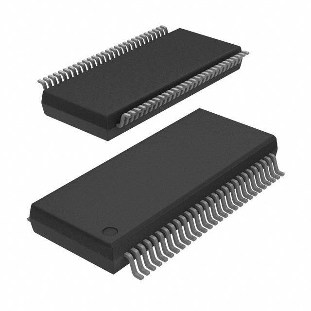
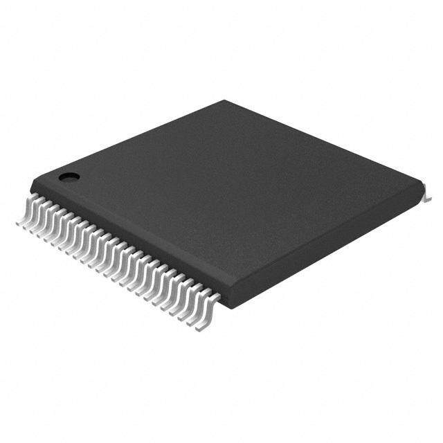
| 供应商器件封装 | 56-SSOP |
| 其它名称 | 425-1844 |
| 包装 | 托盘 |
| 存储器类型 | FLASH |
| 存储容量 | 32M(4M x 8,2M x 16) |
| 封装/外壳 | 56-SOP(0.524",13.30mm) |
| 工作温度 | 0°C ~ 70°C |
| 接口 | 并联 |
| 标准包装 | 40 |
| 格式-存储器 | 闪存 |
| 电压-电源 | 3 V ~ 3.6 V |
| 速度 | 110ns |


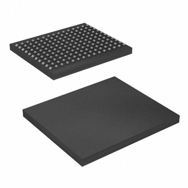
_renders/IS42S32160D-7BLI.jpg)


- 商务部:美国ITC正式对集成电路等产品启动337调查
- 曝三星4nm工艺存在良率问题 高通将骁龙8 Gen1或转产台积电
- 太阳诱电将投资9.5亿元在常州建新厂生产MLCC 预计2023年完工
- 英特尔发布欧洲新工厂建设计划 深化IDM 2.0 战略
- 台积电先进制程称霸业界 有大客户加持明年业绩稳了
- 达到5530亿美元!SIA预计今年全球半导体销售额将创下新高
- 英特尔拟将自动驾驶子公司Mobileye上市 估值或超500亿美元
- 三星加码芯片和SET,合并消费电子和移动部门,撤换高东真等 CEO
- 三星电子宣布重大人事变动 还合并消费电子和移动部门
- 海关总署:前11个月进口集成电路产品价值2.52万亿元 增长14.8%


PDF Datasheet 数据手册内容提取
P S RODUCT PECIFICATIONS Integrated Circuits Group ® LH28F320S3NS-L11 Flash Memory 32M (4MB × 8 / 2MB × 16) (Model No.: LHF32K01) Spec No.: EL108016A Issue Date: December 14, 1998
None
sharp LHF32K01 ●Handle this document carefully for it contains material protected by international copyright law. Any reproduction, full or in part, of this material is prohibited without the express written permission of the company. ●When using the products covered herein, please observe the conditions written herein and the precautions outlined in the following paragraphs. In no event shall the company be liable for any damages resulting from failure to strictly adhere to these conditions and precautions. (1) The products covered herein are designed and manufactured for the following application areas. When using the products covered herein for the equipment listed in Paragraph (2), even for the following application areas, be sure to observe the precautions given in Paragraph (2). Never use the products for the equipment listed in Paragraph (3). •Office electronics •Instrumentation and measuring equipment •Machine tools •Audiovisual equipment •Home appliance •Communication equipment other than for trunk lines (2) Those contemplating using the products covered herein for the following equipment which demands high reliability, should first contact a sales representative of the company and then accept responsibility for incorporating into the design fail-safe operation, redundancy, and other appropriate measures for ensuring reliability and safety of the equipment and the overall system. •Control and safety devices for airplanes, trains, automobiles, and other transportation equipment •Mainframe computers •Traffic control systems •Gas leak detectors and automatic cutoff devices •Rescue and security equipment •Other safety devices and safety equipment, etc. (3) Do not use the products covered herein for the following equipment which demands extremely high performance in terms of functionality, reliability, or accuracy. •Aerospace equipment •Communications equipment for trunk lines •Control equipment for the nuclear power industry •Medical equipment related to life support, etc. (4) Please direct all queries and comments regarding the interpretation of the above three Paragraphs to a sales representative of the company. ●Please direct all queries regarding the products covered herein to a sales representative of the company. Rev. 1.55
sharp LHF32K01 1 CONTENTS PAGE PAGE 1 INTRODUCTION......................................................3 5 DESIGN CONSIDERATIONS.................................31 1.1 Product Overview................................................3 5.1 Three-Line Output Control.................................31 5.2 STS and Block Erase, Full Chip Erase, (Multi) 2 PRINCIPLES OF OPERATION................................6 Word/Byte Write and Block Lock-Bit Configuration 2.1 Data Protection...................................................6 Polling................................................................31 5.3 Power Supply Decoupling..................................31 3 BUS OPERATION....................................................8 5.4 V Trace on Printed Circuit Boards..................31 PP 3.1 Read...................................................................8 5.5 V , V , RP# Transitions.................................32 CC PP 3.2 Output Disable....................................................8 5.6 Power-Up/Down Protection................................32 3.3 Standby...............................................................8 5.7 Power Dissipation..............................................32 3.4 Deep Power-Down..............................................8 3.5 Read Identifier Codes Operation.........................9 6 ELECTRICAL SPECIFICATIONS...........................33 3.6 Query Operation..................................................9 6.1 Absolute Maximum Ratings...............................33 3.7 Write....................................................................9 6.2 Operating Conditions.........................................33 6.2.1 Capacitance.................................................33 4 COMMAND DEFINITIONS.......................................9 6.2.2 AC Input/Output Test Conditions..................34 4.1 Read Array Command.......................................12 6.2.3 DC Characteristics........................................35 4.2 Read Identifier Codes Command......................12 6.2.4 AC Characteristics - Read-Only Operations.37 4.3 Read Status Register Command.......................12 6.2.5 AC Characteristics - Write Operations..........40 4.4 Clear Status Register Command.......................12 6.2.6 Alternative CE#-Controlled Writes................42 4.5 Query Command...............................................13 6.2.7 Reset Operations.........................................44 4.5.1 Block Status Register..................................13 6.2.8 Block Erase, Full Chip Erase, (Multi) 4.5.2 CFI Query Identification String.....................14 Word/Byte Write and Block Lock-Bit 4.5.3 System Interface Information.......................14 Configuration Performance...........................45 4.5.4 Device Geometry Definition.........................15 4.5.5 SCS OEM Specific Extended Query Table..15 7 ADDITIONAL INFORMATION................................47 4.6 Block Erase Command......................................16 7.1 Ordering Information..........................................47 4.7 Full Chip Erase Command................................16 8 PACKAGE AND PACKING SPECIFICATION........48 4.8 Word/Byte Write Command...............................17 4.9 Multi Word/Byte Write Command......................17 4.10 Block Erase Suspend Command.....................18 4.11 (Multi) Word/Byte Write Suspend Command...18 4.12 Set Block Lock-Bit Command..........................19 4.13 Clear Block Lock-Bits Command.....................19 4.14 STS Configuration Command.........................20 Rev. 1.55
sharp LHF32K01 2 LH28F320S3NS-L11 32-MBIT (4MBx8/2MBx16) Smart 3 Flash MEMORY ■ Smart 3 Technology ■ Automated Write and Erase 2.7V or 3.3V V Command User Interface CC 2.7V, 3.3V or 5V V Status Register PP ■ Common Flash Interface (CFI) ■ Enhanced Automated Suspend Options Universal & Upgradable Interface Write Suspend to Read Block Erase Suspend to Write ■ Scalable Command Set (SCS) Block Erase Suspend to Read ■ High Speed Write Performance ■ Enhanced Data Protection Features 32 Bytes x 2 plane Page Buffer Absolute Protection with V =GND PP 2.7 µs/Byte Write Transfer Rate Flexible Block Locking ■ High Speed Read Performance Erase/Write Lockout during Power Transitions 110ns(3.3V±0.3V), 140ns(2.7V-3.6V) ■ Operating Temperature ■ SRAM-Compatible Write Interface 0°C to +70°C ■ User-Configurable x8 or x16 Operation ■ High-Density Symmetrically-Blocked ■ Industry-Standard Packaging Architecture 56-Lead SSOP Sixty-four 64-Kbyte Erasable Blocks ■ Extended Cycling Capability ■ ETOXTM* V Nonvolatile Flash Technology 100,000 Block Erase Cycles 6.4 Million Block Erase Cycles/Chip ■ CMOS Process ■ Low Power Management (P-type silicon substrate) Deep Power-Down Mode ■ Not designed or rated as radiation Automatic Power Savings Mode hardened Decreases I in Static Mode CC SHARP’s LH28F320S3NS-L11 Flash memory with Smart 3 technology is a high-density, low-cost, nonvolatile, read/write storage solution for a wide range of applications. Its symmetrically-blocked architecture, flexible voltage and extended cycling provide for highly flexible component suitable for resident flash arrays, SIMMs and memory cards. Its enhanced suspend capabilities provide for an ideal solution for code + data storage applications. For secure code storage applications, such as networking, where code is either directly executed out of flash or downloaded to DRAM, the LH28F320S3NS-L11 offers three levels of protection: absolute protection with V at PP GND, selective hardware block locking, or flexible software block locking. These alternatives give designers ultimate control of their code security needs. The LH28F320S3NS-L11 is conformed to the flash Scalable Command Set (SCS) and the Common Flash Interface (CFI) specification which enable universal and upgradable interface, enable the highest system/device data transfer rates and minimize device and system-level implementation costs. The LH28F320S3NS-L11 is manufactured on SHARP’s 0.4µm ETOXTM* V process technology. It come in industry- standard package: the 56-Lead SSOP, ideal for board constrained applications. *ETOX is a trademark of Intel Corporation. Rev. 1.55
sharp LHF32K01 3 1 INTRODUCTION or execute code from any other flash memory array location. This datasheet contains LH28F320S3NS-L11 specifications. Section 1 provides a flash memory Individual block locking uses a combination of bits overview. Sections 2, 3, 4, and 5 describe the and WP#, Sixty-four block lock-bits, to lock and memory organization and functionality. Section 6 unlock blocks. Block lock-bits gate block erase, full covers electrical specifications. chip erase and (multi) word/byte write operations. Block lock-bit configuration operations (Set Block 1.1 Product Overview Lock-Bit and Clear Block Lock-Bits commands) set and cleared block lock-bits. The LH28F320S3NS-L11 is a high-performance 32- The status register indicates when the WSM’s block Mbit Smart 3 Flash memory organized as erase, full chip erase, (multi) word/byte write or block 4MBx8/2MBx16. The 4MB of data is arranged in lock-bit configuration operation is finished. sixty-four 64-Kbyte blocks which are individually erasable, lockable, and unlockable in-system. The The STS output gives an additional indicator of WSM memory map is shown in Figure 3. activity by providing both a hardware signal of status (versus software polling) and status masking Smart 3 technology provides a choice of V and CC (interrupt masking for background block erase, for V combinations, as shown in Table 1, to meet PP example). Status polling using STS minimizes both system performance and power expectations. 2.7V CPU overhead and system power consumption. STS V consumes approximately one-fifth the power of CC pin can be configured to different states using the 5V V . V at 2.7V and 3.3V eliminates the need for CC PP Configuration command. The STS pin defaults to a separate 12V converter. In addition to flexible erase RY/BY# operation. When low, STS indicates that the and program voltages, the dedicated V pin gives PP WSM is performing a block erase, full chip erase, complete data protection when V ≤ V . PP PPLK (multi) word/byte write or block lock-bit configuration. STS-High Z indicates that the WSM is ready for a Table 1. V and V Voltage Combinations CC PP new command, block erase is suspended and (multi) Offered by Smart 3 Technology word/byte write are inactive, (multi) word/byte write V Voltage V Voltage CC PP are suspended, or the device is in deep power-down 2.7V 2.7V, 3.3V, 5V mode. The other 3 alternate configurations are all 3.3V 3.3V, 5V pulse mode for use as a system interrupt. Internal V and V detection Circuitry CC PP The access time is 110ns (t ) over the automatically configures the device for optimized AVQV commercial temperature range (0°C to +70°C) and read and write operations. V supply voltage range of 3.0V-3.6V. At lower V CC CC voltage, the access time is 140ns (2.7V-3.6V). A Command User Interface (CUI) serves as the interface between the system processor and internal The Automatic Power Savings (APS) feature operation of the device. A valid command sequence substantially reduces active current when the device written to the CUI initiates device automation. An is in static mode (addresses not switching). In APS internal Write State Machine (WSM) automatically mode, the typical I current is 3 mA at 3.3V V . executes the algorithms and timings necessary for CCR CC block erase, full chip erase, (multi) word/byte write When either CE # or CE #, and RP# pins are at V , and block lock-bit configuration operations. 0 1 CC the I CMOS standby mode is enabled. When the CC RP# pin is at GND, deep power-down mode is A block erase operation erases one of the device’s enabled which minimizes power consumption and 64-Kbyte blocks typically within 0.41s (3.3V V , 5V CC provides write protection during reset. A reset time V ) independent of other blocks. Each block can be PP (t ) is required from RP# switching high until independently erased 100,000 times (6.4 million PHQV outputs are valid. Likewise, the device has a wake block erases per device). Block erase suspend mode time (t ) from RP#-high until writes to the CUI are allows system software to suspend block erase to PHEL recognized. With RP# at GND, the WSM is reset and read or write data from any other block. the status register is cleared. A word/byte write is performed in byte increments The device is available in 56-Lead SSOP (Shrink typically within 12.95µs (3.3V V , 5V V ). A multi CC PP Small Outline Package). Pinout is shown in Figure 2. word/byte write has high speed write performance of 2.7µs/byte (3.3V V , 5V V ). (Multi) Word/byte CC PP write suspend mode enables the system to read data Rev. 1.55
sharp LHF32K01 4 DQ0-DQ15 Output Input Buffer Buffer Query ROM I/O Logic VCC er BYTE# Outputultiplex IRdeengrisiftieerr CE# M RSetgaitsutser DataRegister PageBuffer CRoemgmisatenrd WOEE## RP# Multiplexer WP# Data Comparator A0-A21 BInupffuetr DecYoder Y Gating WMriatec hSitnaete PVrooltgargaem S/Ewriatcshe SVTPPS Address X 64 VCC Latch Decoder 64KByte GND Blocks Address Counter Figure 1. Block Diagram CE0# 1 56 VPP A12 2 55 RP# A13 3 54 A11 A 4 53 A 14 10 A15 5 52 A9 NC 6 51 A1 CE1# 7 50 A2 A21 8 49 A3 A 9 48 A 20 4 A19 10 47 A5 A18 11 46 A6 A17 12 56 LEAD SSOP 45 A7 A16 13 STANDARD PINOUT 44 GND VCC 14 43 A8 GND 15 1.8mm x 16mm x 23.7mm 42 VCC DQ6 16 TOP VIEW 41 DQ9 DQ14 17 40 DQ1 DQ7 18 39 DQ8 DQ15 19 38 DQ0 STS 20 37 A0 OE# 21 36 BYTE# WE# 22 35 NC WP# 23 34 NC DQ13 24 33 DQ2 DQ5 25 32 DQ10 DQ12 26 31 DQ3 DQ4 27 30 DQ11 VCC 28 29 GND Figure 2. SSOP 56-Lead Pinout Rev. 1.55
sharp LHF32K01 5 Table 2. Pin Descriptions Symbol Type Name and Function ADDRESS INPUTS: Inputs for addresses during read and write operations. Addresses are internally latched during a write cycle. A0: Byte Select Address. Not used in x16 mode(can be floated). A -A INPUT 0 21 A1-A4: Column Address. Selects 1 of 16 bit lines. A5-A15: Row Address. Selects 1 of 2048 word lines. A16-A21: Block Address. DATA INPUT/OUTPUTS: DQ -DQ :Inputs data and commands during CUI write cycles; outputs data during memory 0 7 array, status register, query, and identifier code read cycles. Data pins float to high- impedance when the chip is deselected or outputs are disabled. Data is internally latched INPUT/ DQ -DQ during a write cycle. 0 15 OUTPUT DQ -DQ :Inputs data during CUI write cycles in x16 mode; outputs data during memory 8 15 array read cycles in x16 mode; not used for status register, query and identifier code read mode. Data pins float to high-impedance when the chip is deselected, outputs are disabled, or in x8 mode(Byte#=V ). Data is internally latched during a write cycle. IL CHIP ENABLE: Activates the device’s control logic, input buffers decoders, and sense CE #, 0 INPUT amplifiers. Either CE # or CE # V deselects the device and reduces power consumption CE # 0 1 IH 1 to standby levels. Both CE # and CE # must be V to select the devices. 0 1 IL RESET/DEEP POWER-DOWN: Puts the device in deep power-down mode and resets internal automation. RP# V enables normal operation. When driven V , RP# inhibits RP# INPUT IH IL write operations which provides data protection during power transitions. Exit from deep power-down sets the device to read array mode. OE# INPUT OUTPUT ENABLE: Gates the device’s outputs during a read cycle. WRITE ENABLE: Controls writes to the CUI and array blocks. Addresses and data are WE# INPUT latched on the rising edge of the WE# pulse. STS (RY/BY#): Indicates the status of the internal WSM. When configured in level mode (default mode), it acts as a RY/BY# pin. When low, the WSM is performing an internal OPEN operation (block erase, full chip erase, (multi) word/byte write or block lock-bit STS DRAIN configuration). STS High Z indicates that the WSM is ready for new commands, block OUTPUT erase is suspended, and (multi) word/byte write is inactive, (multi) word/byte write is suspended or the device is in deep power-down mode. For alternate configurations of the STATUS pin, see the Configuration command. WP# INPUT WRITE PROTECT: Master control for block locking. When VIL, Locked blocks can not be erased and programmed, and block lock-bits can not be set and reset. BYTE ENABLE: BYTE# V places device in x8 mode. All data is then input or output on IL BYTE# INPUT DQ , and DQ float. BYTE# V places the device in x16 mode , and turns off the A 0-7 8-15 IH 0 input buffer. BLOCK ERASE, FULL CHIP ERASE, (MULTI) WORD/BYTE WRITE, BLOCK LOCK- BIT CONFIGURATION POWER SUPPLY: For erasing array blocks, writing bytes or V SUPPLY configuring block lock-bits. With V ≤V , memory contents cannot be altered. Block PP PP PPLK erase, full chip erase, (multi) word/byte write and block lock-bit configuration with an invalid V (see DC Characteristics) produce spurious results and should not be attempted. PP DEVICE POWER SUPPLY: Internal detection configures the device for 2.7V or 3.3V operation. To switch from one voltage to another, ramp V down to GND and then ramp CC V SUPPLY V to the new voltage. Do not float any power pins. With V ≤V , all write attempts to CC CC CC LKO the flash memory are inhibited. Device operations at invalid V voltage (see DC CC Characteristics) produce spurious results and should not be attempted. GND SUPPLY GROUND: Do not float any ground pins. NC NO CONNECT: Lead is not internal connected; it may be driven or floated. Rev. 1.55
sharp LHF32K01 6 2 PRINCIPLES OF OPERATION Interface software that initiates and polls progress of block erase, full chip erase, (multi) word/byte write The LH28F320S3NS-L11 Flash memory includes an and block lock-bit configuration can be stored in any on-chip WSM to manage block erase, full chip erase, block. This code is copied to and executed from (multi) word/byte write and block lock-bit system RAM during flash memory updates. After configuration functions. It allows for: 100% TTL-level successful completion, reads are again possible via control inputs, fixed power supplies during block the Read Array command. Block erase suspend erase, full chip erase, (multi) word/byte write and allows system software to suspend a block erase to block lock-bit configuration, and minimal processor read or write data from any other block. Write overhead with RAM-Like interface timings. suspend allows system software to suspend a (multi) word/byte write to read data from any other flash After initial device power-up or return from deep memory array location. power-down mode (see Bus Operations), the device defaults to read array mode. Manipulation of external 2.1 Data Protection memory control pins allow array read, standby, and output disable operations. Depending on the application, the system designer may choose to make the V power supply PP Status register, query structure and identifier codes switchable (available only when block erase, full chip can be accessed through the CUI independent of the erase, (multi) word/byte write and block lock-bit V voltage. High voltage on V enables successful configuration are required) or hardwired to V . PP PP PPH1/2/3 block erase, full chip erase, (multi) word/byte write The device accommodates either design practice and and block lock-bit configuration. All functions encourages optimization of the processor-memory associated with altering memory contentsblock interface. erase, full chip erase, (multi) word/byte write and block lock-bit configuration, status, query and When V ≤V , memory contents cannot be PP PPLK identifier codesare accessed via the CUI and altered. The CUI, with multi-step block erase, full chip verified through the status register. erase, (multi) word/byte write and block lock-bit configuration command sequences, provides Commands are written using standard protection from unwanted operations even when high microprocessor write timings. The CUI contents serve voltage is applied to V . All write functions are PP as input to the WSM, which controls the block erase, disabled when V is below the write lockout voltage CC full chip erase, (multi) word/byte write and block lock- V or when RP# is at V . The device’s block LKO IL bit configuration. The internal algorithms are locking capability provides additional protection from regulated by the WSM, including pulse repetition, inadvertent code or data alteration by gating block internal verification, and margining of data. erase, full chip erase and (multi) word/byte write Addresses and data are internally latch during write operations. cycles. Writing the appropriate command outputs array data, accesses the identifier codes, outputs query structure or outputs status register data. Rev. 1.55
sharp LHF32K01 7 1FFFFF 3FFFFF 64-Kbyte Block 31 64-Kbyte Block 63 1F0000 3F0000 1EFFFF 64-Kbyte Block 30 3EFFFF 64-Kbyte Block 62 1E0000 3E0000 1DFFFF 3DFFFF 64-Kbyte Block 29 64-Kbyte Block 61 1D0000 3D0000 1CFFFF 64-Kbyte Block 28 3CFFFF 64-Kbyte Block 60 1C0000 3C0000 1BFFFF 3BFFFF 64-Kbyte Block 27 64-Kbyte Block 59 1B0000 3B0000 1AFFFF 64-Kbyte Block 26 3AFFFF 64-Kbyte Block 58 1A0000 3A0000 19FFFF 64-Kbyte Block 25 39FFFF 64-Kbyte Block 57 190000 390000 18FFFF 64-Kbyte Block 24 38FFFF 64-Kbyte Block 56 180000 380000 17FFFF 64-Kbyte Block 23 37FFFF 64-Kbyte Block 55 170000 370000 16FFFF 64-Kbyte Block 22 36FFFF 64-Kbyte Block 54 160000 360000 15FFFF 64-Kbyte Block 21 35FFFF 64-Kbyte Block 53 150000 350000 14FFFF 64-Kbyte Block 20 34FFFF 64-Kbyte Block 52 140000 340000 13FFFF 64-Kbyte Block 19 33FFFF 64-Kbyte Block 51 130000 330000 12FFFF 64-Kbyte Block 18 32FFFF 64-Kbyte Block 50 120000 320000 11FFFF 64-Kbyte Block 17 31FFFF 64-Kbyte Block 49 110000 310000 10FFFF 64-Kbyte Block 16 30FFFF 64-Kbyte Block 48 100000 300000 0FFFFF 64-Kbyte Block 15 2FFFFF 64-Kbyte Block 47 0F0000 2F0000 0EFFFF 64-Kbyte Block 14 2EFFFF 64-Kbyte Block 46 0E0000 2E0000 0DFFFF 2DFFFF 64-Kbyte Block 13 64-Kbyte Block 45 0D0000 2D0000 0CFFFF 64-Kbyte Block 12 2CFFFF 64-Kbyte Block 44 0C0000 2C0000 0BFFFF 64-Kbyte Block 11 2BFFFF 64-Kbyte Block 43 0B0000 2B0000 0AFFFF 64-Kbyte Block 10 2AFFFF 64-Kbyte Block 42 0A0000 2A0000 09FFFF 64-Kbyte Block 9 29FFFF 64-Kbyte Block 41 090000 290000 08FFFF 64-Kbyte Block 8 28FFFF 64-Kbyte Block 40 080000 280000 07FFFF 64-Kbyte Block 7 27FFFF 64-Kbyte Block 39 070000 270000 06FFFF 64-Kbyte Block 6 26FFFF 64-Kbyte Block 38 060000 260000 05FFFF 64-Kbyte Block 5 25FFFF 64-Kbyte Block 37 050000 250000 04FFFF 64-Kbyte Block 4 24FFFF 64-Kbyte Block 36 040000 240000 03FFFF 64-Kbyte Block 3 23FFFF 64-Kbyte Block 35 030000 230000 02FFFF 64-Kbyte Block 2 22FFFF 64-Kbyte Block 34 020000 220000 01FFFF 64-Kbyte Block 1 21FFFF 64-Kbyte Block 33 010000 210000 00FFFF 64-Kbyte Block 0 20FFFF 64-Kbyte Block 32 000000 200000 Figure 3. Memory Map Rev. 1.55
sharp LHF32K01 8 3 BUS OPERATION block lock-bit configuration, the device continues functioning, and consuming active power until the The local CPU reads and writes flash memory in- operation completes. system. All bus cycles to or from the flash memory conform to standard microprocessor bus cycles. 3.4 Deep Power-Down 3.1 Read RP# at V initiates the deep power-down mode. IL Information can be read from any block, identifier In read modes, RP#-low deselects the memory, codes, query structure, or status register independent places output drivers in a high-impedance state and of the V voltage. RP# must be at V . turns off all internal circuits. RP# must be held low for PP IH a minimum of 100 ns. Time t is required after PHQV The first task is to write the appropriate read mode return from power-down until initial memory access command (Read Array, Read Identifier Codes, Query outputs are valid. After this wake-up interval, normal or Read Status Register) to the CUI. Upon initial operation is restored. The CUI is reset to read array device power-up or after exit from deep power-down mode and status register is set to 80H. mode, the device automatically resets to read array mode. Five control pins dictate the data flow in and During block erase, full chip erase, (multi) word/byte out of the component: CE# (CE #, CE #), OE#, WE#, write or block lock-bit configuration modes, RP#-low 0 1 RP# and WP#. CE #, CE # and OE# must be driven will abort the operation. STS remains low until the 0 1 active to obtain data at the outputs. CE #, CE # is reset operation is complete. Memory contents being 0 1 the device selection control, and when active enables altered are no longer valid; the data may be partially the selected memory device. OE# is the data output erased or written. Time tPHWL is required after RP# (DQ0-DQ15) control and when active drives the goes to logic-high (VIH) before another command can selected memory data onto the I/O bus. WE# and be written. RP# must be at V . Figure 17, 18 illustrates a read IH As with any automated device, it is important to cycle. assert RP# during system reset. When the system comes out of reset, it expects to read from the flash 3.2 Output Disable memory. Automated flash memories provide status information when accessed during block erase, full With OE# at a logic-high level (V ), the device IH chip erase, (multi) word/byte write and block lock-bit outputs are disabled. Output pins DQ -DQ are 0 15 configuration. If a CPU reset occurs with no flash placed in a high-impedance state. memory reset, proper CPU initialization may not occur because the flash memory may be providing 3.3 Standby status information instead of array data. SHARP’s flash memories allow proper CPU initialization Either CE # or CE # at a logic-high level (V ) places 0 1 IH following a system reset through the use of the RP# the device in standby mode which substantially input. In this application, RP# is controlled by the reduces device power consumption. DQ -DQ 0 15 same RESET# signal that resets the system CPU. outputs are placed in a high-impedance state independent of OE#. If deselected during block erase, full chip erase, (multi) word/byte write and Rev. 1.55
sharp LHF32K01 9 3.5 Read Identifier Codes Operation 3.6 Query Operation The read identifier codes operation outputs the The query operation outputs the query structure. manufacturer code, device code, block status codes Query database is stored in the 48Byte ROM. Query for each block (see Figure 4). Using the manufacturer structure allows system software to gain critical and device codes, the system CPU can automatically information for controlling the flash component. match the device with its proper algorithms. The Query structure are always presented on the lowest- block status codes identify locked or unlocked block order data output (DQ -DQ ) only. 0 7 setting and erase completed or erase uncompleted condition. 3.7 Write Writing commands to the CUI enable reading of 3FFFFF device data and identifier codes. They also control inspection and clearing of the status register. When V =V and V =V , the CUI additionally CC CC1/2 PP PPH1/2/3 Reserved for controls block erase, full chip erase, (multi) word/byte Future Implementation write and block lock-bit configuration. 3F0006 The Block Erase command requires appropriate 3F0005 command data and an address within the block to be Block 63 Status Code 3F0004 erased. The Word/byte Write command requires the 3F0003 command and address of the location to be written. Reserved for Set Block Lock-Bit command requires the command Future Implementation and block address within the device (Block Lock) to 3F0000 Block 63 be locked. The Clear Block Lock-Bits command 3EFFFF requires the command and address within the device. (Blocks 2 through 62) 020000 The CUI does not occupy an addressable memory 01FFFF location. It is written when WE# and CE# are active. The address and data needed to execute a command are latched on the rising edge of WE# or CE# Reserved for (whichever goes high first). Standard microprocessor Future Implementation write timings are used. Figures 19 and 20 illustrate WE# and CE#-controlled write operations. 010006 010005 Block 1 Status Code 4 COMMAND DEFINITIONS 010004 010003 Reserved for When the V voltage ≤ V Read operations from PP PPLK, Future Implementation the status register, identifier codes, query, or blocks 010000 Block 1 are enabled. Placing V on V enables PPH1/2/3 PP 00FFFF successful block erase, full chip erase, (multi) word/byte write and block lock-bit configuration Reserved for operations. Future Implementation Device operations are selected by writing specific commands into the CUI. Table 4 defines these 000006 commands. 000005 Block 0 Status Code 000004 000003 Device Code 000002 000001 Manufacturer Code 000000 Block 0 Figure 4. Device Identifier Code Memory Map Rev. 1.55
sharp LHF32K01 10 Table 3. Bus Operations(BYTE#=V ) IH Mode Notes RP# CE # CE # OE# WE# Address V DQ STS 0 1 PP 0-15 Read 1,2,3,9 V V V V V X X D X IH IL IL IL IH OUT Output Disable 3 V V V V V X X High Z X IH IL IL IH IH V V IH IH Standby 3 V V V X X X X High Z X IH IH IL V V IL IH Deep Power-Down 4 V X X X X X X High Z High Z IL Read Identifier See 9 V V V V V X Note 5 High Z Codes IH IL IL IL IH Figure 4 See Table Query 9 V V V V V X Note 6 High Z IH IL IL IL IH 7~11 Write 3,7,8,9 V V V V V X X D X IH IL IL IH IL IN Table 3.1. Bus Operations(BYTE#=V ) IL Mode Notes RP# CE # CE # OE# WE# Address V DQ STS 0 1 PP 0-7 Read 1,2,3,9 V V V V V X X D X IH IL IL IL IH OUT Output Disable 3 V V V V V X X High Z X IH IL IL IH IH V V IH IH Standby 3 V V V X X X X High Z X IH IH IL V V IL IH Deep Power-Down 4 V X X X X X X High Z High Z IL Read Identifier See 9 V V V V V X Note 5 High Z Codes IH IL IL IL IH Figure 4 See Table Query 9 V V V V V X Note 6 High Z IH IL IL IL IH 7~11 Write 3,7,8,9 V V V V V X X D X IH IL IL IH IL IN NOTES: 1. Refer to DC Characteristics. When V ≤V , memory contents can be read, but not altered. PP PPLK 2. X can be V or V for control pins and addresses, and V or V for V . See DC Characteristics for IL IH PPLK PPH1/2/3 PP V and V voltages. PPLK PPH1/2/3 3. STS is V (if configured to RY/BY# mode) when the WSM is executing internal block erase, full chip erase, OL (multi) word/byte write or block lock-bit configuration algorithms. It is floated during when the WSM is not busy, in block erase suspend mode with (multi) word/byte write inactive, (multi) word/byte write suspend mode, or deep power-down mode. 4. RP# at GND±0.2V ensures the lowest deep power-down current. 5. See Section 4.2 for read identifier code data. 6. See Section 4.5 for query data. 7. Command writes involving block erase, full chip erase, (multi) word/byte write or block lock-bit configuration are reliably executed when V =V and V =V . PP PPH1/2/3 CC CC1/2 8. Refer to Table 4 for valid D during a write operation. IN 9. Don’t use the timing both OE# and WE# are V . IL Rev. 1.55
sharp LHF32K01 11 Table 4. Command Definitions(10) Bus Cycles Notes First Bus Cycle Second Bus Cycle Command Req’d Oper(1) Addr(2) Data(3) Oper(1) Addr(2) Data(3) Read Array/Reset 1 Write X FFH Read Identifier Codes ≥2 4 Write X 90H Read IA ID Query ≥2 Write X 98H Read QA QD Read Status Register 2 Write X 70H Read X SRD Clear Status Register 1 Write X 50H Block Erase Setup/Confirm 2 5 Write BA 20H Write BA D0H Full Chip Erase Setup/Confirm 2 Write X 30H Write X D0H Word/Byte Write Setup/Write 2 5,6 Write WA 40H Write WA WD Alternate Word/Byte Write 2 5,6 Write WA 10H Write WA WD Setup/Write Multi Word/Byte Write ≥4 9 Write WA E8H Write WA N-1 Setup/Confirm Block Erase and (Multi) 1 5 Write X B0H Word/byte Write Suspend Confirm and Block Erase and 1 5 Write X D0H (Multi) Word/byte Write Resume Block Lock-Bit Set Setup/Confirm 2 7 Write BA 60H Write BA 01H Block Lock-Bit Reset 2 8 Write X 60H Write X D0H Setup/Confirm STS Configuration Level-Mode for Erase and Write 2 Write X B8H Write X 00H (RY/BY# Mode) STS Configuration 2 Write X B8H Write X 01H Pulse-Mode for Erase STS Configuration 2 Write X B8H Write X 02H Pulse-Mode for Write STS Configuration 2 Write X B8H Write X 03H Pulse-Mode for Erase and Write NOTES: 1. BUS operations are defined in Table 3 and Table 3.1. 2. X=Any valid address within the device. IA=Identifier Code Address: see Figure 4. QA=Query Offset Address. BA=Address within the block being erased or locked. WA=Address of memory location to be written. 3. SRD=Data read from status register. See Table 14 for a description of the status register bits. WD=Data to be written at location WA. Data is latched on the rising edge of WE# or CE# (whichever goes high first). ID=Data read from identifier codes. QD=Data read from query database. 4. Following the Read Identifier Codes command, read operations access manufacturer, device and block status codes. See Section 4.2 for read identifier code data. 5. If the block is locked, WP# must be at V to enable block erase or (multi) word/byte write operations. Attempts IH to issue a block erase or (multi) word/byte write to a locked block while RP# is V . IH 6. Either 40H or 10H are recognized by the WSM as the byte write setup. 7. A block lock-bit can be set while WP# is V . IH 8. WP# must be at V to clear block lock-bits. The clear block lock-bits operation simultaneously clears all block IH lock-bits. 9. Following the Third Bus Cycle, inputs the write address and write data of ’N’ times. Finally, input the confirm command ’D0H’. 10. Commands other than those shown above are reserved by SHARP for future device implementations and should not be used. Rev. 1.55
sharp LHF32K01 12 4.1 Read Array Command 4.3 Read Status Register Command Upon initial device power-up and after exit from deep The status register may be read to determine when a power-down mode, the device defaults to read array block erase, full chip erase, (multi) word/byte write or mode. This operation is also initiated by writing the block lock-bit configuration is complete and whether Read Array command. The device remains enabled the operation completed successfully(see Table 14). for reads until another command is written. Once the It may be read at any time by writing the Read Status internal WSM has started a block erase, full chip Register command. After writing this command, all erase, (multi) word/byte write or block lock-bit subsequent read operations output data from the configuration, the device will not recognize the Read status register until another valid command is written. Array command until the WSM completes its The status register contents are latched on the falling operation unless the WSM is suspended via an Erase edge of OE# or CE#(Either CE # or CE #), 0 1 Suspend and (Multi) Word/byte Write Suspend whichever occurs. OE# or CE#(Either CE # or CE #) 0 1 command. The Read Array command functions must toggle to V before further reads to update the IH independently of the V voltage and RP# must be status register latch. The Read Status Register PP V . command functions independently of the V voltage. IH PP RP# must be V . IH 4.2 Read Identifier Codes Command The extended status register may be read to The identifier code operation is initiated by writing the determine multi word/byte write availability(see Table Read Identifier Codes command. Following the 14.1). The extended status register may be read at command write, read cycles from addresses shown in any time by writing the Multi Word/Byte Write Figure 4 retrieve the manufacturer, device, block lock command. After writing this command, all subsequent configuration and block erase status (see Table 5 for read operations output data from the extended status identifier code values). To terminate the operation, register, until another valid command is written. Multi write another valid command. Like the Read Array Word/Byte Write command must be re-issued to command, the Read Identifier Codes command update the extended status register latch. functions independently of the V voltage and RP# PP must be V . Following the Read Identifier Codes 4.4 Clear Status Register Command IH command, the following information can be read: Status register bits SR.5, SR.4, SR.3 and SR.1 are Table 5. Identifier Codes set to "1"s by the WSM and can only be reset by the Address Clear Status Register command. These bits indicate Code Data A21-A0 various failure conditions (see Table 14). By allowing 000000 system software to reset these bits, several Manufacture Code B0 000001 operations (such as cumulatively erasing or locking 000002 multiple blocks or writing several bytes in sequence) Device Code D4 000003 may be performed. The status register may be polled X0004(1) to determine if an error occurs during the sequence. Block Status Code X0005(1) •Block is Unlocked DQ =0 To clear the status register, the Clear Status Register 0 command (50H) is written. It functions independently •Block is Locked DQ =1 0 of the applied V Voltage. RP# must be V . This •Last erase operation PP IH DQ =0 command is not functional during block erase, full completed successfully 1 chip erase, (multi) word/byte write block lock-bit •Last erase operation did configuration, block erase suspend or (multi) DQ =1 not completed successfully 1 word/byte write suspend modes. •Reserved for Future Use DQ 2-7 NOTE: 1. X selects the specific block status code to be read. See Figure 4 for the device identifier code memory map. Rev. 1.55
sharp LHF32K01 13 4.5 Query Command Table 6. Example of Query Structure Output Mode Offset Address Output Query database can be read by writing Query DQ DQ 15~8 7~0 command (98H). Following the command write, read A , A , A , A , A , A 5 4 3 2 1 0 cycle from address shown in Table 7~11 retrieve the 1 , 0 , 0 , 0 , 0 , 0 (20H) High-Z "Q" critical information to write, erase and otherwise X8 mode 1 , 0 , 0 , 0 , 0 , 1 (21H) High-Z "Q" control the flash component. A of query offset 1, 0 , 0 , 0 , 1 , 0 (22H) High-Z "R" 0 address is ignored when X8 mode (BYTE#=V ). 1 , 0 , 0 , 0 , 1 , 1 (23H) High-Z "R" IL A , A , A , A , A 5 4 3 2 1 Query data are always presented on the low-byte X16 mode 1 , 0 , 0 , 0 , 0 (10H) 00H "Q" data output (DQ -DQ ). In x16 mode, high-byte 1 , 0 , 0 , 0 , 1 (11H) 00H "R" 0 7 (DQ -DQ ) outputs 00H. The bytes not assigned to 8 15 any information or reserved for future use are set to "0". This command functions independently of the V voltage. RP# must be V . PP IH 4.5.1 Block Status Register This field provides lock configuration and erase status for the specified block. These informations are only available when device is ready (SR.7=1). If block erase or full chip erase operation is finished irregulary, block erase status bit will be set to "1". If bit 1 is "1", this block is invalid. Table 7. Query Block Status Register Offset Length Description (Word Address) (BA+2)H 01H Block Status Register bit0 Block Lock Configuration 0=Block is unlocked 1=Block is Locked bit1 Block Erase Status 0=Last erase operation completed successfully 1=Last erase operation not completed successfully bit2-7 reserved for future use Note: 1. BA=The beginning of a Block Address. Rev. 1.55
sharp LHF32K01 14 4.5.2 CFI Query Identification String The Identification String provides verification that the component supports the Common Flash Interface specification. Additionally, it indicates which version of the spec and which Vendor-specified command set(s) is(are) supported. Table 8. CFI Query Identification String Offset Length Description (Word Address) 10H,11H,12H 03H Query Unique ASCII string "QRY" 51H,52H,59H 13H,14H 02H Primary Vendor Command Set and Control Interface ID Code 01H,00H (SCS ID Code) 15H,16H 02H Address for Primary Algorithm Extended Query Table 31H,00H (SCS Extended Query Table Offset) 17H,18H 02H Alternate Vendor Command Set and Control Interface ID Code 0000H (0000H means that no alternate exists) 19H,1AH 02H Address for Alternate Algorithm Extended Query Table 0000H (0000H means that no alternate exists) 4.5.3 System Interface Information The following device information can be useful in optimizing system interface software. Table 9. System Information String Offset Length Description (Word Address) 1BH 01H V Logic Supply Minimum Write/Erase voltage CC 27H (2.7V) 1CH 01H V Logic Supply Maximum Write/Erase voltage CC 36H (3.6V) 1DH 01H V Programming Supply Minimum Write/Erase voltage PP 27H (2.7V) 1EH 01H V Programming Supply Maximum Write/Erase voltage PP 55H (5.5V) 1FH 01H Typical Timeout per Single Byte/Word Write 04H (24=16µs) 20H 01H Typical Timeout for Maximum Size Buffer Write (32 Bytes) 06H (26=64µs) 21H 01H Typical Timeout per Individual Block Erase 09H (09H=9, 29=512ms) 22H 01H Typical Timeout for Full Chip Erase 0FH (0FH=15, 215=32768ms) 23H 01H Maximum Timeout per Single Byte/Word Write, 2N times of typical. 04H (24=16, 16µsx16=256µs) 24H 01H Maximum Timeout Maximum Size Buffer Write, 2N times of typical. 04H (24=16, 64µsx16=1024µs) 25H 01H Maximum Timeout per Individual Block Erase, 2N times of typical. 04H (24=16, 1024msx16=16384ms) 26H 01H Maximum Timeout for Full Chip Erase, 2N times of typical. 04H (24=16, 32768msx16=524288ms) Rev. 1.55
sharp LHF32K01 15 4.5.4 Device Geometry Definition This field provides critical details of the flash device geometry. Table 10. Device Geometry Definition Offset Length Description (Word Address) 27H 01H Device Size 16H (16H=22, 222=4194304=4M Bytes) 28H,29H 02H Flash Device Interface description 02H,00H (x8/x16 supports x8 and x16 via BYTE#) 2AH,2BH 02H Maximum Number of Bytes in Multi-byte 05H,00H (25=32 Bytes ) 2CH 01H Number of Erase Block Regions within device 01H (symmetrically blocked) 2DH,2EH 02H The Number of Erase Blocks 3FH,00H (3FH=63 ==> 63+1=64 Blocks) 2FH,30H 02H The Number of "256 Bytes" cluster in a Erase block 00H,01H (0100H=256 ==>256 Bytes x 256= 64K Bytes in a Erase Block) 4.5.5 SCS OEM Specific Extended Query Table Certain flash features and commands may be optional in a vendor-specific algorithm specification. The optional vendor-specific Query table(s) may be used to specify this and other types of information. These structures are defined solely by the flash vendor(s). Table 11. SCS OEM Specific Extended Query Table Offset Length Description (Word Address) 31H,32H,33H 03H PRI 50H,52H,49H 34H 01H 31H (1) Major Version Number , ASCII 35H 01H 30H (0) Minor Version Number, ASCII 36H,37H, 04H 0FH,00H,00H,00H 38H,39H Optional Command Support bit0=1 : Chip Erase Supported bit1=1 : Suspend Erase Supported bit2=1 : Suspend Write Supported bit3=1 : Lock/Unlock Supported bit4=0 : Queued Erase Not Supported bit5-31=0 : reserved for future use 3AH 01H 01H Supported Functions after Suspend bit0=1 : Write Supported after Erase Suspend bit1-7=0 : reserved for future use 3BH,3CH 02H 03H,00H Block Status Register Mask bit0=1 : Block Status Register Lock Bit [BSR.0] active bit1=1 : Block Status Register Valid Bit [BSR.1] active bit2-15=0 : reserved for future use 3DH 01H V Logic Supply Optimum Write/Erase voltage(highest performance) CC 33H(3.3V) 3EH 01H V Programming Supply Optimum Write/Erase voltage(highest performance) PP 50H(5.0V) 3FH reserved Reserved for future versions of the SCS Specification Rev. 1.55
sharp LHF32K01 16 4.6 Block Erase Command erase setup is first written, followed by a full chip erase confirm. After a confirm command is written, Block erase is executed one block at a time and device erases the all unlocked blocks from block 0 to initiated by a two-cycle command. A block erase Block 63 block by block. This command sequence setup is first written, followed by an block erase requires appropriate sequencing. Block confirm. This command sequence requires preconditioning, erase and verify are handled appropriate sequencing and an address within the internally by the WSM (invisible to the system). After block to be erased (erase changes all block data to the two-cycle full chip erase sequence is written, the FFH). Block preconditioning, erase and verify are device automatically outputs status register data handled internally by the WSM (invisible to the when read (see Figure 6). The CPU can detect full system). After the two-cycle block erase sequence is chip erase completion by analyzing the output data of written, the device automatically outputs status the STS pin or status register bit SR.7. register data when read (see Figure 5). The CPU can detect block erase completion by analyzing the When the full chip erase is complete, status register output data of the STS pin or status register bit SR.7. bit SR.5 should be checked. If erase error is detected, the status register should be cleared before When the block erase is complete, status register bit system software attempts corrective actions. The CUI SR.5 should be checked. If a block erase error is remains in read status register mode until a new detected, the status register should be cleared before command is issued. If error is detected on a block system software attempts corrective actions. The CUI during full chip erase operation, WSM stops erasing remains in read status register mode until a new the block and begin to erase the next block. Reading command is issued. the block valid status by issuing Read ID Codes command or Query command informs which blocks This two-step command sequence of set-up followed failed to its erase. by execution ensures that block contents are not accidentally erased. An invalid Block Erase command This two-step command sequence of set-up followed sequence will result in both status register bits SR.4 by execution ensures that block contents are not and SR.5 being set to "1". Also, reliable block erasure accidentally erased. An invalid Full Chip Erase can only occur when V =V and V =V . command sequence will result in both status register CC CC1/2 PP PPH1/2/3 In the absence of this high voltage, block contents bits SR.4 and SR.5 being set to "1". Also, reliable full are protected against erasure. If block erase is chip erasure can only occur when VCC=VCC1/2 and attempted while VPP≤VPPLK, SR.3 and SR.5 will be VPP=VPPH1/2/3. In the absence of this high voltage, block contents are protected against erasure. If full set to "1". Successful block erase requires that the corresponding block lock-bit be cleared or if set, that chip erase is attempted while VPP≤VPPLK, SR.3 and WP#=VIH. If block erase is attempted when the SR.5 will be set to "1". When WP#=VIH, all blocks are corresponding block lock-bit is set and WP#=V , erased independent of block lock-bits status. When IL SR.1 and SR.5 will be set to "1". WP#=VIL, only unlocked blocks are erased. Full chip erase can not be suspended. 4.7 Full Chip Erase Command This command followed by a confirm command (D0H) erases all of the unlocked blocks. A full chip Rev. 1.55
sharp LHF32K01 17 4.8 Word/Byte Write Command continue monitoring XSR.7 by writing multi word/byte write setup with write address until XSR.7 transitions Word/byte write is executed by a two-cycle command to 1. When XSR.7 transitions to 1, the device is ready sequence. Word/Byte Write setup (standard 40H or for loading the data to the buffer. A word/byte count alternate 10H) is written, followed by a second write (N)-1 is written with write address. After writing a that specifies the address and data (latched on the word/byte count(N)-1, the device automatically turns rising edge of WE#). The WSM then takes over, back to output status register data. The word/byte controlling the word/byte write and write verify count (N)-1 must be less than or equal to 1FH in x8 algorithms internally. After the word/byte write mode (0FH in x16 mode). On the next write, device sequence is written, the device automatically outputs start address is written with buffer data. Subsequent status register data when read (see Figure 7). The writes provide additional device address and data, CPU can detect the completion of the word/byte write depending on the count. All subsequent address event by analyzing the STS pin or status register bit must lie within the start address plus the count. After SR.7. the final buffer data is written, write confirm (D0H) must be written. This initiates WSM to begin copying When word/byte write is complete, status register bit the buffer data to the Flash Array. An invalid Multi SR.4 should be checked. If word/byte write error is Word/Byte Write command sequence will result in detected, the status register should be cleared. The both status register bits SR.4 and SR.5 being set to internal WSM verify only detects errors for "1"s that "1". For additional multi word/byte write, write another do not successfully write to "0"s. The CUI remains in multi word/byte write setup and check XSR.7. The read status register mode until it receives another Multi Word/Byte Write command can be queued command. while WSM is busy as long as XSR.7 indicates "1", because LH28F320S3NS-L11 has two buffers. If an Reliable word/byte writes can only occur when error occurs while writing, the device will stop writing V =V and V =V . In the absence of and flush next multi word/byte write command loaded CC CC1/2 PP PPH1/2/3 this high voltage, memory contents are protected in multi word/byte write command. Status register bit against word/byte writes. If word/byte write is SR.4 will be set to "1". No multi word/byte write attempted while V ≤V , status register bits SR.3 command is available if either SR.4 or SR.5 are set PP PPLK and SR.4 will be set to "1". Successful word/byte to "1". SR.4 and SR.5 should be cleared before write requires that the corresponding block lock-bit be issuing multi word/byte write command. If a multi cleared or, if set, that WP#=V . If word/byte write is word/byte write command is attempted past an erase IH attempted when the corresponding block lock-bit is block boundary, the device will write the data to Flash set and WP#=V , SR.1 and SR.4 will be set to "1". Array up to an erase block boundary and then stop IL Word/byte write operations with V <WP#<V writing. Status register bits SR.4 and SR.5 will be set IL IH produce spurious results and should not be to "1". attempted. Reliable multi byte writes can only occur when 4.9 Multi Word/Byte Write Command VCC=VCC1/2 and VPP=VPPH1/2/3. In the absence of this high voltage, memory contents are protected against multi word/byte writes. If multi word/byte write Multi word/byte write is executed by at least four- is attempted while V ≤V , status register bits cycle or up to 35-cycle command sequence. Up to PP PPLK 32 bytes in x8 mode (16 words in x16 mode) can be SR.3 and SR.4 will be set to "1". Successful multi loaded into the buffer and written to the Flash Array. word/byte write requires that the corresponding block First, multi word/byte write setup (E8H) is written with lock-bit be cleared or, if set, that WP#=VIH. If multi the write address. At this point, the device byte write is attempted when the corresponding block automatically outputs extended status register data lock-bit is set and WP#=VIL, SR.1 and SR.4 will be (XSR) when read (see Figure 8, 9). If extended set to "1". status register bit XSR.7 is 0, no Multi Word/Byte Write command is available and multi word/byte write setup which just has been written is ignored. To retry, Rev. 1.55
sharp LHF32K01 18 4.10 Block Erase Suspend Command until (multi) word/byte write operations initiated during block erase suspend have completed. The Block Erase Suspend command allows block- erase interruption to read or (multi) word/byte-write 4.11 (Multi) Word/Byte Write Suspend data in another block of memory. Once the block- Command erase process starts, writing the Block Erase Suspend command requests that the WSM suspend The (Multi) Word/Byte Write Suspend command the block erase sequence at a predetermined point in allows (multi) word/byte write interruption to read data the algorithm. The device outputs status register data in other flash memory locations. Once the (multi) when read after the Block Erase Suspend command word/byte write process starts, writing the (Multi) is written. Polling status register bits SR.7 and SR.6 Word/Byte Write Suspend command requests that can determine when the block erase operation has the WSM suspend the (multi) word/byte write been suspended (both will be set to "1"). STS will sequence at a predetermined point in the algorithm. also transition to High Z. Specification tWHRH2 defines The device continues to output status register data the block erase suspend latency. when read after the (Multi) Word/Byte Write Suspend command is written. Polling status register bits SR.7 At this point, a Read Array command can be written and SR.2 can determine when the (multi) word/byte to read data from blocks other than that which is write operation has been suspended (both will be set suspended. A (Multi) Word/Byte Write command to "1"). STS will also transition to High Z. sequence can also be issued during erase suspend Specification t defines the (multi) word/byte WHRH1 to program data in other blocks. Using the (Multi) write suspend latency. Word/Byte Write Suspend command (see Section 4.11), a (multi) word/byte write operation can also be At this point, a Read Array command can be written suspended. During a (multi) word/byte write operation to read data from locations other than that which is with block erase suspended, status register bit SR.7 suspended. The only other valid commands while will return to "0" and the STS (if set to RY/BY#) (multi) word/byte write is suspended are Read Status output will transition to VOL. However, SR.6 will Register and (Multi) Word/Byte Write Resume. After remain "1" to indicate block erase suspend status. (Multi) Word/Byte Write Resume command is written to the flash memory, the WSM will continue the The only other valid commands while block erase is (multi) word/byte write process. Status register bits suspended are Read Status Register and Block SR.2 and SR.7 will automatically clear and STS will Erase Resume. After a Block Erase Resume return to V . After the (Multi) Word/Byte Write OL command is written to the flash memory, the WSM command is written, the device automatically outputs will continue the block erase process. Status register status register data when read (see Figure 11). V PP bits SR.6 and SR.7 will automatically clear and STS must remain at V (the same V level used PPH1/2/3 PP will return to VOL. After the Erase Resume command for (multi) word/byte write) while in (multi) word/byte is written, the device automatically outputs status write suspend mode. WP# must also remain at V or IH register data when read (see Figure 10). VPP must VIL. remain at V (the same V level used for PPH1/2/3 PP block erase) while block erase is suspended. RP# must also remain at V . Block erase cannot resume IH Rev. 1.6
sharp LHF32K01 19 4.12 Set Block Lock-Bit Command block lock-bits can be cleared using only the Clear Block Lock-Bits command. See Table 13 for a A flexible block locking and unlocking scheme is summary of hardware and software write protection enabled via block lock-bits. The block lock-bits gate options. program and erase operations With WP#=V , IH individual block lock-bits can be set using the Set Clear block lock-bits operation is executed by a two- Block Lock-Bit command. See Table 13 for a cycle command sequence. A clear block lock-bits summary of hardware and software write protection setup is first written. After the command is written, the options. device automatically outputs status register data when read (see Figure 13). The CPU can detect Set block lock-bit is executed by a two-cycle completion of the clear block lock-bits event by command sequence. The set block lock-bit setup analyzing the STS Pin output or status register bit along with appropriate block or device address is SR.7. written followed by either the set block lock-bit confirm (and an address within the block to be When the operation is complete, status register bit locked). The WSM then controls the set block lock-bit SR.5 should be checked. If a clear block lock-bit error algorithm. After the sequence is written, the device is detected, the status register should be cleared. automatically outputs status register data when read The CUI will remain in read status register mode until (see Figure 12). The CPU can detect the completion another command is issued. of the set block lock-bit event by analyzing the STS This two-step sequence of set-up followed by pin output or status register bit SR.7. execution ensures that block lock-bits are not When the set block lock-bit operation is complete, accidentally cleared. An invalid Clear Block Lock-Bits status register bit SR.4 should be checked. If an error command sequence will result in status register bits is detected, the status register should be cleared. SR.4 and SR.5 being set to "1". Also, a reliable clear The CUI will remain in read status register mode until block lock-bits operation can only occur when a new command is issued. VCC=VCC1/2 and VPP=VPPH1/2/3. If a clear block lock- bits operation is attempted while V ≤V , SR.3 PP PPLK This two-step sequence of set-up followed by and SR.5 will be set to "1". In the absence of this high execution ensures that block lock-bits are not voltage, the block lock-bits content are protected accidentally set. An invalid Set Block Lock-Bit against alteration. A successful clear block lock-bits command will result in status register bits SR.4 and operation requires WP#=V . If it is attempted with IH SR.5 being set to "1". Also, reliable operations occur WP#=V , SR.1 and SR.5 will be set to "1" and the IL only when V =V and V =V . In the operation will fail. Clear block lock-bits operations CC CC1/2 PP PPH1/2/3 absence of this high voltage, block lock-bit contents with V <RP# produce spurious results and should IH are protected against alteration. not be attempted. A successful set block lock-bit operation requires If a clear block lock-bits operation is aborted due to WP#=V . If it is attempted with WP#=V , SR.1 and V or V transitioning out of valid range or RP# IH IL PP CC SR.4 will be set to "1" and the operation will fail. Set active transition, block lock-bit values are left in an block lock-bit operations with WP#<V produce undetermined state. A repeat of clear block lock-bits IH spurious results and should not be attempted. is required to initialize block lock-bit contents to known values. 4.13 Clear Block Lock-Bits Command All set block lock-bits are cleared in parallel via the Clear Block Lock-Bits command. With WP#=V , IH Rev. 1.55
sharp LHF32K01 20 4.14 STS Configuration Command Table 12. STS Configuration Coding Description Configuration Effects The Status (STS) pin can be configured to different Bits states using the STS Configuration command. Once Set STS pin to default level mode the STS pin has been configured, it remains in that (RY/BY#). RY/BY# in the default 00H configuration until another configuration command is level-mode of operation will indicate issued, the device is powered down or RP# is set to WSM status condition. V . Upon initial device power-up and after exit from Set STS pin to pulsed output signal IL deep power-down mode, the STS pin defaults to for specific erase operation. In this RY/BY# operation where STS low indicates that the mode, STS provides low pulse at 01H WSM is busy. STS High Z indicates that the WSM is the completion of BLock Erase, ready for a new operation. Full Chip Erase and Clear Block Lock-bits operations. To reconfigure the STS pin to other modes, the STS Set STS pin to pulsed output signal Configuration is issued followed by the appropriate for a specific write operation. In this configuration code. The three alternate configurations 02H mode, STS provides low pulse at are all pulse mode for use as a system interrupt. The the completion of (Multi) Byte Write STS Configuration command functions independently and Set Block Lock-bit operation. of the V voltage and RP# must be V . Set STS pin to pulsed output signal PP IH for specific write and erase operation. STS provides low pulse 03H at the completion of Block Erase, Full Chip Erase, (Multi) Word/Byte Write and Block Lock-bit Configuration operations. Table 13. Write Protection Alternatives Block Operation WP# Effect Lock-Bit Block Erase, 0 V or V Block Erase and (Multi) Word/Byte Write Enabled IL IH (Multi) Word/Byte Block is Locked. Block Erase and (Multi) Word/Byte Write 1 V Write IL Disabled Block Lock-Bit Override. Block Erase and (Multi) Word/Byte V IH Write Enabled Full Chip Erase 0,1 V All unlocked blocks are erased, locked blocks are not erased IL X V All blocks are erased IH Set Block Lock-Bit X V Set Block Lock-Bit Disabled IL V Set Block Lock-Bit Enabled IH Clear Block Lock-Bits X V Clear Block Lock-Bits Disabled IL V Clear Block Lock-Bits Enabled IH Rev. 1.55
sharp LHF32K01 21 Table 14. Status Register Definition WSMS BESS ECBLBS WSBLBS VPPS WSS DPS R 7 6 5 4 3 2 1 0 NOTES: SR.7 = WRITE STATE MACHINE STATUS 1 = Ready Check STS or SR.7 to determine block erase, full chip 0 = Busy erase, (multi) word/byte write or block lock-bit configuration completion. SR.6 = BLOCK ERASE SUSPEND STATUS SR.6-0 are invalid while SR.7="0". 1 = Block Erase Suspended 0 = Block Erase in Progress/Completed If both SR.5 and SR.4 are "1"s after a block erase, full chip erase, (multi) word/byte write, block lock-bit SR.5 = ERASE AND CLEAR BLOCK LOCK-BITS configuration or STS configuration attempt, an improper STATUS command sequence was entered. 1 = Error in Erase or Clear Blocl Lock-Bits 0 = Successful Erase or Clear Block Lock-Bits SR.3 does not provide a continuous indication of V PP level. The WSM interrogates and indicates the V level PP SR.4 = WRITE AND SET BLOCK LOCK-BIT STATUS only after block erase, full chip erase, (multi) word/byte 1 = Error in Write or Set Block Lock-Bit write or block lock-bit configuration command 0 = Successful Write or Set Block Lock-Bit sequences. SR.3 is not guaranteed to reports accurate feedback only when V ≠V . PP PPH1/2/3 SR.3 = V STATUS PP 1 = VPP Low Detect, Operation Abort SR.1 does not provide a continuous indication of block 0 = VPP OK lock-bit values. The WSM interrogates block lock-bit, and WP# only after block erase, full chip erase, (multi) SR.2 = WRITE SUSPEND STATUS word/byte write or block lock-bit configuration command 1 = Write Suspended sequences. It informs the system, depending on the 0 = Write in Progress/Completed attempted operation, if the block lock-bit is set and/or WP# is not V . Reading the block lock configuration IH SR.1 = DEVICE PROTECT STATUS codes after writing the Read Identifier Codes command 1 = Block Lock-Bit and/or WP# Lock Detected, indicates block lock-bit status. Operation Abort 0 = Unlock SR.0 is reserved for future use and should be masked out when polling the status register. SR.0 = RESERVED FOR FUTURE ENHANCEMENTS Table 14.1. Extended Status Register Definition SMS R R R R R R R 7 6 5 4 3 2 1 0 NOTES: XSR.7 = STATE MACHINE STATUS 1 = Multi Word/Byte Write available After issue a Multi Word/Byte Write command: XSR.7 0 = Multi Word/Byte Write not available indicates that a next Multi Word/Byte Write command is available. XSR.6-0=RESERVED FOR FUTURE ENHANCEMENTS XSR.6-0 is reserved for future use and should be masked out when polling the extended status register. Rev. 1.55
sharp LHF32K01 22 Start Bus Command Comments Operation Write 70H Read Status Data=70H Write Register Addr=X Read Status Read Status Register Data Register Check SR.7 Standby 1=WSM Ready 0 SR.7= 0=WSM Busy 1 Write Erase Setup Data=20H Addr=Within Block to be Erased Write 20H, Block Address Erase Data=D0H Write Confirm Addr=Within Block to be Erased Write D0H, Block Address Read Status Register Data Read Status Register Check SR.7 Suspend Block Standby 1=WSM Ready No Erase Loop 0=WSM Busy 0 Suspend SR.7= Repeat for subsequent block erasures. Block Erase Yes Full status check can be done after each block erase or after a sequence of 1 block erasures. Write FFH after the last operation to place device in read array mode. Full Status Check if Desired Block Erase Complete FULL STATUS CHECK PROCEDURE Read Status Register Bus Data(See Above) Command Comments Operation Check SR.3 Standby SR.3= 1 VPPRange Error 1=VPP Error Detect Check SR.1 0 1=Device Protect Detect Standby WP#=VIL,Block Lock-Bit is Set 1 Only required for systems SR.1= Device Protect Error implementing lock-bit configuration 0 Check SR.4,5 Standby Both 1=Command Sequence Error 1 Command Sequence Check SR.5 SR.4,5= Standby Error 1=Block Erase Error 0 SR.5,SR.4,SR.3 and SR.1 are only cleared by the Clear Status Register Command in cases where multiple blocks are erased 1 before full status is checked. SR.5= Block Erase Error If error is detected, clear the Status Register before attempting retry or other error recovery. 0 Block Erase Successful Figure 5. Automated Block Erase Flowchart Rev. 1.55
sharp LHF32K01 23 Start Bus Command Comments Operation Write 70H Read Status Data=70H Write Register Addr=X Read Status Read Status Register Data Register Check SR.7 Standby 1=WSM Ready 0 SR.7= 0=WSM Busy 1 Full Chip Erase Data=30H Write Setup Addr=X Write 30H Full Chip Erase Data=D0H Write Confirm Addr=X Write D0H Read Status Register Data Read Status Check SR.7 Register Standby 1=WSM Ready 0=WSM Busy Full status check can be done after each full chip erase. 0 SR.7= Write FFH after the last operation to place device in read array mode. 1 Full Status Check if Desired Full Chip Erase Complete FULL STATUS CHECK PROCEDURE Read Status Register Bus Data(See Above) Command Comments Operation Check SR.3 SR.3= 1 VPPRange Error Standby 1=VPP Error Detect Check SR.4,5 0 Standby Both 1=Command Sequence Error 1 Command Sequence Standby Check SR.5 SR.4,5= 1=Full Chip Erase Error Error 0 SR.5,SR.4,SR.3 and SR.1 are only cleared by the Clear Status Register Command in cases where multiple blocks are erased before full status is checked. 1 If error is detected, clear the Status Register before attempting SR.5= Full Chip Erase Error retry or other error recovery. 0 Full Chip Erase Successful Figure 6. Automated Full Chip Erase Flowchart Rev. 1.55
sharp LHF32K01 24 Start Bus Command Comments Operation Read Status Data=70H Write 70H Write Register Addr=X Read Status Read Status Register Data Register Check SR.7 Standby 1=WSM Ready 0 0=WSM Busy SR.7= Setup Word/Byte Data=40H or 10H 1 Write Write Addr=Location to Be Written Write 40H or 10H, Data=Data to Be Written Address Write Word/Byte Write Addr=Location to Be Written Write Word/Byte Data and Address Read Status Register Data Read Check SR.7 Status Register Standby 1=WSM Ready Suspend Word/Byte 0=WSM Busy No Write Loop 0 Suspend Repeat for subsequent word/byte writes. SR.7= Word/Byte Yes SR full status check can be done after each word/byte write, or after a sequence of Write word/byte writes. 1 Write FFH after the last word/byte write operation to place device in read array mode. Full Status Check if Desired Word/byte Write Complete FULL STATUS CHECK PROCEDURE Read Status Register Bus Data(See Above) Command Comments Operation Check SR.3 Standby SR.3= 1 VPPRange Error 1=VPP Error Detect Check SR.1 0 1=Device Protect Detect Standby WP#=VIL,Block Lock-Bit is Set 1 Only required for systems SR.1= Device Protect Error implementing lock-bit configuration 0 Check SR.4 Standby 1=Data Write Error 1 SR.4,SR.3 and SR.1 are only cleared by the Clear Status Register SR.4= Word/byte Write Error command in cases where multiple locations are written before full status is checked. 0 If error is detected, clear the Status Register before attempting retry or other error recovery. Word/Byte Write Successful Figure 7. Automated Word/byte Write Flowchart Rev. 1.55
sharp LHF32K01 25 Start Write E8H, Bus Start Address Command Comments Operation Read Extend Setup Data=E8H Write Status Register Multi Word/Byte Write Addr=Start Address No Read Extended Status Register Data 0 Write Buffer Yes XSR.7= Time Out Check XSR.7 1 Standby 1=Multi Word/Byte Write Ready 0=Multi Word/Byte Write Busy Write Word or Byte Count (N)-1, Start Address Write Data=Word or Byte Count (N)-1 (Note1) Addr=Start Address Write Buffer Data, Start Address Write Data=Buffer Data (Note2,3) Addr=Start Address X=0 Write Data=Buffer Data (Note4,5) Addr=Device Address Data=D0H Write Addr=X Abort Buffer Yes Write Another Write Commnad? Block Address Read Status Register Data No Multi Word/Byte Write Write Buffer Data, Abort Check SR.7 Device Address Standby 1=WSM Ready 0=WSM Busy Yes 1. Byte or word count values on DQ0-7 are loaded into the count register. X = N 2. Write Buffer contents will be programmed at the start address. 3. Align the start address on a Write Buffer boundary for maximum No programming performance. 4.The device aborts the Multi Word/Byte Write command if the current address is X=X+1 outside of the original block address. 5.The Status Register indicates an "improper command sequence" if the Multi Word/Byte command is aborted. Follow this with a Clear Status Register command. SR full status check can be done after each multi word/byte write, Write D0H or after a sequence of multi word/byte writes. Write FFH after the last multi word/byte write operation to place device in read array mode. Another Yes Buffer Write ? No Read Status Register No Suspend Multi Word/Byte Write Loop 0 Suspend Yes SR.7= Multi Word/Byte Write 1 Full Status Check if Desired Multi Word/Byte Write Complete Figure 8. Automated Multi Word/Byte Write Flowchart Rev. 1.6
sharp LHF32K01 26 FULL STATUS CHECK PROCEDURE FOR MULTI WORD/BYTE WRITE OPERATION Bus Read Status Register Command Comments Operation Check SR.3 Standby 1 1=VPP Error Detect SR.3= VPPRange Error Check SR.1 0 1=Device Protect Detect Standby WP#=VIL,Block Lock-Bit is Set Only required for systems 1 implementing lock-bit configuration SR.1= Device Protect Error Check SR.4,5 0 Standby Both 1=Command Sequence Error 1 Command Sequence Standby Check SR.4 SR.4,5= 1=Data Write Error Error 0 SR.5,SR.4,SR.3 and SR.1 are only cleared by the Clear Status Register command in cases where multiple locations are written before full status is checked. 1 Multi Word/Byte Write If error is detected, clear the Status Register before attempting SR.4= Error retry or other error recovery. 0 Multi Word/Byte Write Successful Figure 9. Full Status Check Procedure for Automated Multi Word/Byte Write Rev. 1.55
sharp LHF32K01 27 Start Bus Command Comments Operation Erase Data=B0H Write Write B0H Suspend Addr=X Status Register Data Read Addr=X Read Status Register Check SR.7 Standby 1=WSM Ready 0=WSM Busy 0 SR.7= Check SR.6 Standby 1=Block Erase Suspended 1 0=Block Erase Completed Erase Data=D0H Write Resume Addr=X 0 SR.6= Block Erase Completed 1 Read Read or (Multi) Word/Byte Write Write ? Read Array Data (Multi) Word/Byte Write Loop No Done? Yes Write D0H Write FFH Block Erase Resumed Read Array Data Figure 10. Block Erase Suspend/Resume Flowchart Rev. 1.55
sharp LHF32K01 28 Start Bus Command Comments Operation (Multi) Word/Byte Write Data=B0H Write B0H Write Suspend Addr=X Status Register Data Read Read Addr=X Status Register Check SR.7 Standby 1=WSM Ready 0=WSM Busy 0 SR.7= Check SR.2 1=(Multi) Word/Byte Write 1 Standby Suspended 0=(Multi) Word/Byte Write Completed 0 (Multi) Word/Byte Write SR.2= Data=FFH Completed Write Read Array Addr=X 1 Read Array locations other Read than that being written. Write FFH (Multi) Word/Byte Write Data=D0H Write Resume Addr=X Read Array Data Done No Reading Yes Write D0H Write FFH (Multi) Word/Byte Write Read Array Data Resumed Figure 11. (Multi) Word/Byte Write Suspend/Resume Flowchart Rev. 1.55
sharp LHF32K01 29 Start Bus Command Comments Operation Write 60H, Set Block Data=60H Write Block Address Lock-Bit Setup Addr=Block Address Write 01H, Set Block Data=01H, Block Address Write Lock-Bit Confirm Addr=Block Address Read Status Register Read Status Register Data Check SR.7 0 SR.7= Standby 1=WSM Ready 0=WSM Busy 1 Repeat for subsequent block lock-bit set operations. Full status check can be done after each block lock-bit set operation Full Status or after a sequence of block lock-bit set operations. Check if Desired Write FFH after the last block lock-bit set operation to place device in read array mode. Set Block Lock-Bit Complete FULL STATUS CHECK PROCEDURE Read Status Register Bus Data(See Above) Command Comments Operation Check SR.3 Standby 1 1=VPP Error Detect SR.3= VPPRange Error Check SR.1 0 Standby 1=Device Protect Detect WP#=VIL Check SR.4,5 1 SR.1= Device Protect Error Standby Both 1=Command Sequence Error 0 Check SR.4 Standby 1=Set Block Lock-Bit Error 1 Command Sequence SR.4,5= SR.5,SR.4,SR.3 and SR.1 are only cleared by the Clear Status Error Register command in cases where multiple block lock-bits are set before 0 full status is checked. If error is detected, clear the Status Register before attempting retry or other error recovery. 1 SR.4= Set Block Lock-Bit Error 0 Set Block Lock-Bit Successful Figure 12. Set Block Lock-Bit Flowchart Rev. 1.55
sharp LHF32K01 30 Start Bus Command Comments Operation Clear Block Data=60H Write Write 60H Lock-Bits Setup Addr=X Clear Block Data=D0H Write Lock-Bits Confirm Addr=X Write D0H Read Status Register Data Read Status Register Check SR.7 Standby 1=WSM Ready 0=WSM Busy 0 SR.7= Write FFH after the Clear Block Lock-Bits operation to place device in read array mode. 1 Full Status Check if Desired Clear Block Lock-Bits Complete FULL STATUS CHECK PROCEDURE Read Status Register Bus Data(See Above) Command Comments Operation Check SR.3 Standby 1 1=VPP Error Detect SR.3= VPPRange Error Check SR.1 0 Standby 1=Device Protect Detect WP#=VIL 1 Check SR.4,5 SR.1= Device Protect Error Standby Both 1=Command Sequence Error 0 Check SR.5 Standby 1=Clear Block Lock-Bits Error 1 Command Sequence SR.4,5= SR.5,SR.4,SR.3 and SR.1 are only cleared by the Clear Status Error Register command. 0 If error is detected, clear the Status Register before attempting retry or other error recovery. 1 Clear Block Lock-Bits SR.5= Error 0 Clear Block Lock-Bits Successful Figure 13. Clear Block Lock-Bits Flowchart Rev. 1.55
sharp LHF32K01 31 5 DESIGN CONSIDERATIONS STS, in default mode, is also High-Z when the device is in block erase suspend (with (multi) word/byte write 5.1 Three-Line Output Control inactive), (multi) word/byte write suspend or deep power-down modes. The device will often be used in large memory arrays. 5.3 Power Supply Decoupling SHARP provides three control inputs to accommodate multiple memory connections. Three- Line control provides for: Flash memory power switching characteristics require careful device decoupling. System designers are a. Lowest possible memory power dissipation. interested in three supply current issues; standby current levels, active current levels and transient b. Complete assurance that data bus contention will peaks produced by falling and rising edges of CE# not occur. and OE#. Transient current magnitudes depend on the device outputs’ capacitive and inductive loading. To use these control inputs efficiently, an address Two-line control and proper decoupling capacitor decoder should enable CE# while OE# should be selection will suppress transient voltage peaks. Each connected to all memory devices and the system’s device should have a 0.1 µF ceramic capacitor READ# control line. This assures that only selected connected between its V and GND and between its memory devices have active outputs while CC V and GND. These high-frequency, low inductance deselected memory devices are in standby mode. PP capacitors should be placed as close as possible to RP# should be connected to the system package leads. Additionally, for every eight devices, POWERGOOD signal to prevent unintended writes a 4.7 µF electrolytic capacitor should be placed at the during system power transitions. POWERGOOD array’s power supply connection between V and should also toggle during system reset. CC GND. The bulk capacitor will overcome voltage slumps caused by PC board trace inductance. 5.2 STS and Block Erase, Full Chip Erase, (Multi) Word/Byte Write and 5.4 V Trace on Printed Circuit Boards PP Block Lock-Bit Configuration Polling Updating flash memories that reside in the target STS is an open drain output that should be system requires that the printed circuit board connected to V by a pullup resistor to provide a designer pay attention to the V Power supply trace. CC PP hardware method of detecting block erase, full chip The V pin supplies the memory cell current for PP erase, (multi) word/byte write and block lock-bit block erase, full chip erase, (multi) word/byte write configuration completion. In default mode, it and block lock-bit configuration. Use similar trace transitions low after block erase, full chip erase, widths and layout considerations given to the V CC (multi) word/byte write or block lock-bit configuration power bus. Adequate V supply traces and PP commands and returns to V when the WSM has decoupling will decrease V voltage spikes and OH PP finished executing the internal algorithm. For overshoots. alternate STS pin configurations, see the Configuration command. STS can be connected to an interrupt input of the system CPU or controller. It is active at all times. Rev. 1.55
sharp LHF32K01 32 5.5 V , V , RP# Transitions powers-up first. Internal circuitry resets the CUI to CC PP read array mode at power-up. Block erase, full chip erase, (multi) word/byte write and block lock-bit configuration are not guaranteed if A system designer must guard against spurious VPP falls outside of a valid VPPH1/2/3 range, VCC falls writes for VCC voltages above VLKO when VPP is outside of a valid V range, or RP#=V . If V active. Since both WE# and CE# must be low for a CC1/2 IL PP error is detected, status register bit SR.3 is set to "1" command write, driving either to VIHwill inhibit writes. along with SR.4 or SR.5, depending on the attempted The CUI’s two-step command sequence architecture operation. If RP# transitions to V during block provides added level of protection against data IL erase, full chip erase, (multi) word/byte write or block alteration. lock-bit configuration, STS(if set to RY/BY# mode) In-system block lock and unlock capability prevents will remain low until the reset operation is complete. inadvertent data alteration. The device is disabled Then, the operation will abort and the device will while RP#=V regardless of its control inputs state. enter deep power-down. The aborted operation may IL leave data partially altered. Therefore, the command 5.7 Power Dissipation sequence must be repeated after normal operation is restored. Device power-off or RP# transitions to V IL clear the status register. When designing portable systems, designers must consider battery power consumption not only during The CUI latches commands issued by system device operation, but also for data retention during software and is not altered by V or CE# transitions system idle time. Flash memory’s nonvolatility PP or WSM actions. Its state is read array mode upon increases usable battery life because data is retained power-up, after exit from deep power-down or after when system power is removed. V transitions below V . CC LKO In addition, deep power-down mode ensures After block erase, full chip erase, (multi) word/byte extremely low power consumption even when system write or block lock-bit configuration, even after V power is applied. For example, portable computing PP transitions down to V , the CUI must be placed in products and other power sensitive applications that PPLK read array mode via the Read Array command if use an array of devices for solid-state storage can subsequent access to the memory array is desired. consume negligible power by lowering RP# to V IL standby or sleep modes. If access is again needed, 5.6 Power-Up/Down Protection the devices can be read following the t and PHQV t wake-up cycles required after RP# is first PHWL The device is designed to offer protection against raised to VIH. See AC Characteristics Read Only accidental block and full chip erasure, (multi) and Write Operations and Figures 17, 18, 19, 20 for word/byte writing or block lock-bit configuration during more information. power transitions. Upon power-up, the device is indifferent as to which power supply (V or V ) PP CC Rev. 1.55
sharp LHF32K01 33 6 ELECTRICAL SPECIFICATIONS *WARNING: Stressing the device beyond the "Absolute Maximum Ratings" may cause permanent 6.1 Absolute Maximum Ratings* damage. These are stress ratings only. Operation beyond the "Operating Conditions" is not recommended and extended exposure beyond the Operating Temperature "Operating Conditions" may affect device reliability. During Read, Erase, Write and Block Lock-Bit Configuration........0°C to +70°C(1) NOTES: Temperature under Bias...............-10°C to +80°C 1. Operating temperature is for commercial temperature product defined by this specification. Storage Temperature........................-65°C to +125°C 2. All specified voltages are with respect to GND. Minimum DC voltage is -0.5V on input/output pins Voltage On Any Pin (except V , V )...............-0.5V to V +0.5V(2) and -0.2V on VCC and VPP pins. During CC PP CC transitions, this level may undershoot to -2.0V for V Suply Voltage............................-0.2V to +7.0V(2) periods <20ns. Maximum DC voltage on CC input/output pins and V is V +0.5V which, CC CC during transitions, may overshoot to V +2.0V for V Update Voltage during CC PP periods <20ns. Erase, Write and Block Lock-Bit Configuration......-0.2V to +7.0V(2) 3. Output shorted for no more than one second. No more than one output shorted at a time. Output Short Circuit Current........................100mA(3) 6.2 Operating Conditions Temperature and V Operating Conditions CC Symbol Parameter Min. Max. Unit Test Condition T Operating Temperature 0 +70 °C Ambient Temperature A V V Supply Voltage (2.7V-3.6V) 2.7 3.6 V CC1 CC V V Supply Voltage (3.3V±0.3V) 3.0 3.6 V CC2 CC 6.2.1 CAPACITANCE(1) T =+25°C, f=1MHz A Symbol Parameter Typ. Max. Unit Condition C Input Capacitance 7 10 pF V =0.0V IN IN C Output Capacitance 9 12 pF V =0.0V OUT OUT NOTE: 1. Sampled, not 100% tested. Rev. 1.55
sharp LHF32K01 34 6.2.2 AC INPUT/OUTPUT TEST CONDITIONS 2.7 INPUT 1.35 TEST POINTS 1.35 OUTPUT 0.0 AC test inputs are driven at 2.7V for a Logic "1" and 0.0V for a Logic "0." Input timing begins, and output timing ends, at 1.35V. Input rise and fall times (10% to 90%) <10 ns. Figure 14. Transient Input/Output Reference Waveform for V =2.7V-3.6V CC 3.0 INPUT 1.5 TEST POINTS 1.5 OUTPUT 0.0 AC test inputs are driven at 3.0V for a Logic "1" and 0.0V for a Logic "0." Input timing begins, and output timing ends, at 1.5V. Input rise and fall times (10% to 90%) <10 ns. Figure 15. Transient Input/Output Reference Waveform for V =3.3V±0.3V CC Test Configuration Capacitance Loading Value 1.3V Test Configuration C (pF) L 1N914 VCC=3.3V±0.3V, 2.7V-3.6V 50 RL=3.3kΩ DEVICE UNDER OUT TEST CL Includes Jig CL Capacitance Figure 16. Transient Equivalent Testing Load Circuit Rev. 1.6
sharp LHF32K01 35 6.2.3 DC CHARACTERISTICS DC Characteristics V =2.7V V =3.3V Test CC CC Sym. Parameter Notes Typ. Max. Typ. Max. Unit Conditions I Input Load Current 1 V =V Max. LI ±0.5 ±0.5 µA CC CC V =V or GND IN CC I Output Leakage Current 1 V =V Max. LO ±0.5 ±0.5 µA CC CC V =V or GND OUT CC I V Standby Current 1,3,6 CMOS Inputs CCS CC 20 100 20 100 µA V =V Max. CC CC CE#=RP#=V ±0.2V CC TTL Inputs 1 4 1 4 mA V =V Max. CC CC CE#=RP#=V IH I V Deep Power-Down 1 RP#=GND±0.2V CCD CC 20 20 µA Current I (STS)=0mA OUT I V Read Current 1,5,6 CMOS Inputs CCR CC V =V Max., 30 30 mA CC CC CE#=GND f=5MHz, I =0mA OUT TTL Inputs 35 35 mA V =V Max., CE#=V CC CC IL f=5MHz, I =0mA OUT I V Write Current 1,7 17 mA V =2.7V-3.6V CCW CC PP ((Multi) W/B Write or 17 17 mA V =3.3V±0.3V PP Set Block Lock Bit) 17 17 mA V =5.0V±0.5V PP I V Erase Current 1,7 17 mA V =2.7V-3.6V CCE CC PP (Block Erase, Full Chip 17 17 mA V =3.3V±0.3V PP Erase, Clear Block Lock Bits) 17 17 mA V =5.0V±0.5V PP I V Write or Block Erase 1,2 CCWS CC 1 6 1 6 mA CE#=V I Suspend Current IH CCES I V Standby Current 1 ±2 ±15 ±2 ±15 µA V ≤V PPS PP PP CC I V Read Current 1 10 200 10 200 µA V >V PPR PP PP CC I V Deep Power-Down 1 PPD PP 0.1 5 0.1 5 µA RP#=GND±0.2V Current I V Write Current 1,7 80 mA V =2.7V-3.6V PPW PP PP ((Multi) W/B Write or 80 80 mA V =3.3V±0.3V PP Set Block Lock Bit) 80 80 mA V =5.0V±0.5V PP I V Erase Current 1,7 40 mA V =2.7V-3.6V PPE PP PP (Block Erase, Full Chip 40 40 mA V =3.3V±0.3V PP Erase, Clear Block Lock Bits) 40 40 mA V =5.0V±0.5V PP I V Write or Block Erase 1 PPWS PP 10 200 10 200 µA V =V I Suspend Current PP PPH1/2/3 PPES Rev. 1.55
sharp LHF32K01 36 DC Characteristics (Continued) V =2.7V V =3.3V Test CC CC Sym. Parameter Notes Min. Max. Min. Max. Unit Conditions V Input Low Voltage 7 -0.5 0.8 -0.5 0.8 V IL V Input High Voltage 7 V V IH 2.0 CC 2.0 CC V +0.5 +0.5 V Output Low Voltage 3,7 V =V Min. OL 0.4 0.4 V CC CC I =2mA OL V Output High Voltage 3,7 V =V Min. OH1 2.4 2.4 V CC CC (TTL) I =-2.5mA OH V Output High Voltage 3,7 0.85 0.85 V =V Min. OH2 V CC CC (CMOS) V V I =-2.5mA CC CC OH V V V =V Min. CC CC V CC CC -0.4 -0.4 I =-100µA OH V V Lockout Voltage during 4,7 PPLK PP 1.5 1.5 V Normal Operations V V Voltage during Write or PPH1 PP 2.7 3.6 V Erase Operations V V Voltage during Write or PPH2 PP 3.0 3.6 3.0 3.6 V Erase Operations V V Voltage during Write or PPH3 PP 4.5 5.5 4.5 5.5 V Erase Operations V V Lockout Voltage 2.0 2.0 V LKO CC NOTES: 1. All currents are in RMS unless otherwise noted. Typical values at nominal V voltage and T =+25°C.These CC A currents are valid for all product versions (packages and speeds). 2. I and I are specified with the device de-selected. If read or byte written while in erase suspend mode, CCWS CCES the device’s current draw is the sum of I or I and I or I , respectively. CCWS CCES CCR CCW 3. Includes STS. 4. Block erases, full chip erases, (multi) word/byte writes and block lock-bit configurations are inhibited when V ≤V , and not guaranteed in the range between V (max.) and V (min.), between V (max.) and PP PPLK PPLK PPH1 PPH1 V (min.), between V (max.) and V (min.) and above V (max.). PPH2 PPH2 PPH3 PPH3 5. Automatic Power Savings (APS) reduces typical I to 3mA at 2.7V and 3.3V V in static operation. CCR CC 6. CMOS inputs are either V ±0.2V or GND±0.2V. TTL inputs are either V or V . CC IL IH 7. Sampled, not 100% tested. Rev. 1.55
sharp LHF32K01 37 6.2.4 AC CHARACTERISTICS - READ-ONLY OPERATIONS(1) V =2.7V-3.6V, T =0°C to +70°C CC A Versions(4) LH28F320S3-L140 Sym. Parameter Notes Min. Max. Unit t Read Cycle Time 140 ns AVAV t Address to Output Delay 140 ns AVQV t CE# to Output Delay 2 140 ns ELQV t RP# High to Output Delay 600 ns PHQV t OE# to Output Delay 2 50 ns GLQV t CE# to Output in Low Z 3 0 ns ELQX t CE# High to Output in High Z 3 50 ns EHQZ t OE# to Output in Low Z 3 0 ns GLQX t OE# High to Output in High Z 3 20 ns GHQZ t Output Hold from Address, CE# or OE# Change, OH 3 0 ns Whichever Occurs First t BYTE# to Output Delay FLQV 3 140 ns t FHQV t BYTE# to Output in High Z 3 30 ns FLQZ t CE# Low to BYTE# High or Low ELFL 3 5 ns t ELFH NOTE: See 3.3V V Read-Only Operations for notes 1 through 4. CC V =3.3V±0.3V, T =0°C to +70°C CC A Versions(4) LH28F320S3-L110 Sym. Parameter Notes Min. Max. Unit t Read Cycle Time 110 ns AVAV t Address to Output Delay 110 ns AVQV t CE# to Output Delay 2 110 ns ELQV t RP# High to Output Delay 600 ns PHQV t OE# to Output Delay 2 45 ns GLQV t CE# to Output in Low Z 3 0 ns ELQX t CE# High to Output in High Z 3 50 ns EHQZ t OE# to Output in Low Z 3 0 ns GLQX t OE# High to Output in High Z 3 20 ns GHQZ t Output Hold from Address, CE# or OE# Change, OH 3 0 ns Whichever Occurs First t BYTE# to Output Delay FLQV 3 110 ns t FHQV t BYTE# to Output in High Z 3 30 ns FLQZ t CE# Low to BYTE# High or Low ELFL 3 5 ns t ELFH NOTES: 1. See AC Input/Output Reference Waveform for maximum allowable input slew rate. 2. OE# may be delayed up to t -t after the falling edge of CE# without impact on t . ELQV GLQV ELQV 3. Sampled, not 100% tested. 4. See Ordering Information for device speeds (valid operational combinations). Rev. 1.55
sharp LHF32K01 38 Device Standby Address Selection Data Valid V IH ADDRESSES(A) Address Stable V IL t AVAV V IH CE#(E) t V EHQZ IL V IH OE#(G) t GHQZ V IL V IH WE#(W) t GLQV VIL tELQV t t OH GLQX t ELQX V OH HIGH Z HIGH Z DATA(D/Q) Valid Output V OL t AVQV VCC t PHQV V IH RP#(P) V IL NOTE:CE# is defined as the latter of CE # and CE # going Low or the first of CE # or CE # going High. 0 1 0 1 Figure 17. AC Waveform for Read Operations Rev. 1.55
sharp LHF32K01 39 Device Standby Address Selection Data Valid V IH ADDRESSES(A) Address Stable V IL t AVAV V IH CE#(E) t V EHQZ IL tAVFL=tELFL V IH OE#(G) VIL tELFL tGHQZ VIH tFLQV=tAVQV BYTE#(F) t GLQV VIL tELQV t t OH GLQX t ELQX V OH DATA(D/Q) HIGH Z Valid HIGH Z Data Output (DQ0-DQ7) Output V OL t AVQV t FLQZ V OH DATA(D/Q) HIGH Z Data HIGH Z (DQ8-DQ15) Output V OL NOTE: CE# is defined as the latter of CE # and CE # going Low or the first of CE # or CE # going High. 0 1 0 1 Figure 18. BYTE# Timing Waveforms Rev. 1.55
sharp LHF32K01 40 6.2.5 AC CHARACTERISTICS - WRITE OPERATIONS(1) V =2.7V-3.6V, T =0°C to +70°C CC A Versions(5) LH28F320S3-L140 Sym. Parameter Notes Min. Max. Unit t Write Cycle Time 140 ns AVAV t RP# High Recovery to WE# Going Low 2 1 µs PHWL t CE# Setup to WE# Going Low 10 ns ELWL t WE# Pulse Width 55 ns WLWH t WP# V Setup to WE# Going High 2 100 ns SHWH IH t V Setup to WE# Going High 2 100 ns VPWH PP t Address Setup to WE# Going High 3 50 ns AVWH t Data Setup to WE# Going High 3 50 ns DVWH t Data Hold from WE# High 5 ns WHDX t Address Hold from WE# High 5 ns WHAX t CE# Hold from WE# High 10 ns WHEH t WE# Pulse Width High 30 ns WHWL t WE# High to STS Going Low 100 ns WHRL t Write Recovery before Read 0 ns WHGL t V Hold from Valid SRD, STS High Z 2,4 0 ns QVVL PP t WP# V Hold from Valid SRD, STS High Z 2,4 0 ns QVSL IH NOTE: See 3.3V V WE#-Controlled Writes for notes 1 through 5. CC V =3.3V±0.3V, T =0°C to +70°C CC A Versions(5) LH28F320S3-L110 Sym. Parameter Notes Min. Max. Unit t Write Cycle Time 110 ns AVAV t RP# High Recovery to WE# Going Low 2 1 µs PHWL t CE# Setup to WE# Going Low 10 ns ELWL t WE# Pulse Width 55 ns WLWH t WP# V Setup to WE# Going High 2 100 ns SHWH IH t V Setup to WE# Going High 2 100 ns VPWH PP t Address Setup to WE# Going High 3 50 ns AVWH t Data Setup to WE# Going High 3 50 ns DVWH t Data Hold from WE# High 5 ns WHDX t Address Hold from WE# High 5 ns WHAX t CE# Hold from WE# High 10 ns WHEH t WE# Pulse Width High 30 ns WHWL t WE# High to STS Going Low 100 ns WHRL t Write Recovery before Read 0 ns WHGL t V Hold from Valid SRD, STS High Z 2,4 0 ns QVVL PP t WP# V Hold from Valid SRD, STS High Z 2,4 0 ns QVSL IH NOTES: 1. Read timing characteristics during block erase, full chip erase, (multi) wrod/byte write and block lock-bit configuration operations are the same as during read-only operations. Refer to AC Characteristics for read-only operations. 2. Sampled, not 100% tested. 3. Refer to Table 4 for valid A and D for block erase, full chip erase, (multi) word/byte write or block lock-bit IN IN configuration. 4. V should be held at V until determination of block erase, full chip erase, (multi) word/byte write or PP PPH1/2/3 block lock-bit configuration success (SR.1/3/4/5=0). 5. See Ordering Information for device speeds (valid operational combinations). Rev. 1.55
sharp LHF32K01 41 1 2 3 4 5 6 }}}}}} V IH ADDRESSES(A) AIN AIN V IL t tAVAV tAVWH WHAX V IH CE#(E) V IL tELWL tWHEH tWHGL V IH OE#(G) V IL tWHWL tWHQV1,2,3,4 V IH WE#(W) VIL tWLWH t DVWH VIH High Z tWHDX Valid DATA(D/Q) DIN DIN SRD DIN V IL t PHWL t High Z WHRL STS(R) V OL t t SHWH QVSL V IH WP#(S) V IL V IH RP#(P) V IL t VPWH t V QVVL PPH3,2,1 VPP(V) VPPLK NOTES: V IL 1. V power-up and standby. CC 2. Write erase or write setup. 3. Write erase confirm or valid address and data. 4. Automated erase or program delay. 5. Read status register data. 6. Write Read Array command. 7. CE# is defined as the latter of CE # and CE # going Low or the first of CE # or CE # going High. 0 1 0 1 Figure 19. AC Waveform for WE#-Controlled Write Operations Rev. 1.55
sharp LHF32K01 42 6.2.6 ALTERNATIVE CE#-CONTROLLED WRITES(1) V =2.7V-3.6V, T =0°C to +70°C CC A Versions(5) LH28F320S3-L140 Sym. Parameter Notes Min. Max. Unit t Write Cycle Time 140 ns AVAV t RP# High Recovery to CE# Going Low 2 1 µs PHEL t WE# Setup to CE# Going Low 0 ns WLEL t CE# Pulse Width 70 ns ELEH t WP# V Setup to CE# Going High 2 100 ns SHEH IH t V Setup to CE# Going High 2 100 ns VPEH PP t Address Setup to CE# Going High 3 50 ns AVEH t Data Setup to CE# Going High 3 50 ns DVEH t Data Hold from CE# High 5 ns EHDX t Address Hold from CE# High 5 ns EHAX t WE# Hold from CE# High 0 ns EHWH t CE# Pulse Width High 25 ns EHEL t CE# High to STS Going Low 100 ns EHRL t Write Recovery before Read 0 ns EHGL t V Hold from Valid SRD, STS High Z 2,4 0 ns QVVL PP t WP# V Hold from Valid SRD, STS High Z 2,4 0 ns QVSL IH NOTE: See 3.3V V Alternative CE#-Controlled Writes for notes 1 through 5. CC V =3.3V±0.3V, T =0°C to +70°C CC A Versions(5) LH28F320S3-L110 Sym. Parameter Notes Min. Max. Unit t Write Cycle Time 110 ns AVAV t RP# High Recovery to CE# Going Low 2 1 µs PHEL t WE# Setup to CE# Going Low 0 ns WLEL t CE# Pulse Width 70 ns ELEH t WP# V Setup to CE# Going High 2 100 ns SHEH IH t V Setup to CE# Going High 2 100 ns VPEH PP t Address Setup to CE# Going High 3 50 ns AVEH t Data Setup to CE# Going High 3 50 ns DVEH t Data Hold from CE# High 5 ns EHDX t Address Hold from CE# High 5 ns EHAX t WE# Hold from CE# High 0 ns EHWH t CE# Pulse Width High 25 ns EHEL t CE# High to STS Going Low 100 ns EHRL t Write Recovery before Read 0 ns EHGL t V Hold from Valid SRD, STS High Z 2,4 0 ns QVVL PP t WP# V Hold from Valid SRD, STS High Z 2,4 0 ns QVSL IH NOTES: 1. In systems where CE# defines the write pulse width (within a longer WE# timing waveform), all setup, hold and inactive WE# times should be measured relative to the CE# waveform. 2. Sampled, not 100% tested. 3. Refer to Table 4 for valid A and D for block erase, full chip erase, (multi) word/byte write or block lock-bit IN IN configuration. 4. V should be held at V until determination of block erase, full chip erase, (multi) word/byte write or PP PPH1/2/3 block lock-bit configuration success (SR.1/3/4/5=0). 5. See Ordering Information for device speeds (valid operational combinations). Rev. 1.55
sharp LHF32K01 43 1 2 3 4 5 6 }}}}}} V IH ADDRESSES(A) AIN AIN V IL t tAVAV tAVEH EHAX V IH WE#(W) V IL tWLEL tEHWH tEHGL V IH OE#(G) V IL t t EHEL EHQV1,2,3,4 V IH CE#(E) VIL tELEH t DVEH VIH High Z tEHDX Valid DATA(D/Q) DIN DIN SRD DIN V IL t PHEL t High Z EHRL STS(R) V OL tSHEH tQVSL V IH WP#(S) V IL V IH RP#(P) V IL t VPEH t V QVVL PPH3,2,1 VPP(V) VPPLK NOTES: V IL 1. V power-up and standby. CC 2. Write erase or write setup. 3. Write erase confirm or valid address and data. 4. Automated erase or program delay. 5. Read status register data. 6. Write Read Array command. 7. CE# is defined as the latter of CE # and CE # going Low or the first of CE # or CE # going High. 0 1 0 1 Figure 20. AC Waveform for CE#-Controlled Write Operations Rev. 1.55
sharp LHF32K01 44 6.2.7 RESET OPERATIONS High Z STS(R) V OL V IH RP#(P) V IL t PLPH (A)Reset During Read Array Mode High Z STS(R) V OL t PLRH V IH RP#(P) V IL t PLPH (B)Reset During Block Erase, Full Chip Erase, (Multi) Word/Byte Write or Block Lock-Bit Configuretion 2.7/3.3V V CC V IL t 23VPH V IH RP#(P) V IL (C)V Power Up Timing CC Figure 21. AC Waveform for Reset Operation Reset AC Specifications(1) V =2.7V V =3.3V CC CC Symbol Parameter Notes Min. Max. Min. Max. Unit t RP# Pulse Low Time PLPH (If RP# is tied to V , this specification is 100 100 ns CC not applicable) t RP# Low to Reset during Block Erase, PLRH Full Chip Erase, (Multi) Word/Byte Write 2,3 21.5 21.1 µs or Block Lock-Bit Configuration t V at 2.7V to RP# High 23VPH CC 4 100 100 ns V at 3.0V to RP# High CC NOTES: 1. These specifications are valid for all product versions (packages and speeds). 2. If RP# is asserted while a block erase, full chip erase, (multi) word/byte write or block lock-bit configuration operation is not executing, the reset will complete within 100ns. 3. A reset time, t , is required from the latter of STS going High Z or RP# going high until outputs are valid. PHQV 4. When the device power-up, holding RP# low minimum 100ns is required after V has been in predefined range CC and also has been in stable there. Rev. 1.55
sharp LHF32K01 45 6.2.8 BLOCK ERASE, FULL CHIP ERASE, (MULTI) WORD/BYTE WRITE AND BLOCK LOCK-BIT CONFIGURATION PERFORMANCE(3,4) V =2.7V-3.6V, T =0°C to +70°C CC A V =2.7V-3.6V V =3.0V-3.6V V =4.5V-5.5V PP PP PP Sym. Parameter Notes Typ.(1) Max. Typ.(1) Max. Typ.(1) Max. Unit Word/Byte Write Time t WHQV1 (using W/B write, in word 2 22.19 250 22.19 250 13.2 180 µs t EHQV1 mode) Word/Byte Write Time t WHQV1 (using W/B write, in byte 2 19.9 250 19.9 250 13.2 180 µs t EHQV1 mode) Word/Byte Write Time 2 5.76 250 5.76 250 2.76 180 µs (using multi word/byte write) Block Write Time (using W/B write, in word 2 0.73 8.2 0.73 8.2 0.44 4.8 s mode) Block Write Time (using W/B write, in byte 2 1.31 16.5 1.31 16.5 0.87 10.9 s mode) Block Write Time 2 0.37 4.1 0.37 4.1 0.18 2 s (using multi word/byte write) t WHQV2 Block Erase Time 2 0.56 10 0.56 10 0.42 10 s t EHQV2 Full Chip Erase Time 35.9 640 35.9 640 26.9 640 s t WHQV3 Set Block Lock-Bit Time 2 22.17 250 22.17 250 13.2 180 µs t EHQV3 t WHQV4 Clear Block Lock-Bits Time 2 0.56 10 0.56 10 0.42 10 s t EHQV4 t Write Suspend Latency Time WHRH1 7.24 10.2 7.24 10.2 6.73 9.48 µs t to Read EHRH1 t Erase Suspend Latency WHRH2 15.5 21.5 15.5 21.5 12.54 17.54 µs t Time to Read EHRH2 NOTE: See 3.3V V Block Erase, Full Chip Erase, (Multi) Word/Byte Write and Block Lock-Bit Configuration Performance CC for notes 1 through 4. Rev. 1.55
sharp LHF32K01 46 V =3.3V±0.3V, T =0°C to +70°C CC A V =3.0V-3.6V V =4.5V-5.5V PP PP Sym. Parameter Notes Typ.(1) Max. Typ.(1) Max. Unit t Word/Byte Write Time WHQV1 2 21.75 250 12.95 180 µs t (using W/B write, in word mode) EHQV1 t Word/Byte Write Time WHQV1 2 19.51 250 12.95 180 µs t (using W/B write, in byte mode) EHQV1 Word/Byte Write Time 2 5.66 250 2.7 180 µs (using multi word/byte write) Block Write Time 2 0.72 8.2 0.43 4.8 s (using W/B write, in word mode) Block Write Time 2 1.28 16.5 0.85 10.9 s (using W/B write, in byte mode) Block Write Time 2 0.36 4.1 0.18 2 s (using multi word/byte write) t WHQV2 Block Erase Time 2 0.55 10 0.41 10 s t EHQV2 Full Chip Erase Time 35.2 640 26.3 640 s t WHQV3 Set Block Lock-Bit Time 2 21.75 250 12.95 180 µs t EHQV3 t WHQV4 Clear Block Lock-Bits Time 2 0.55 10 0.41 10 s t EHQV4 t WHRH1 Write Suspend Latency Time to Read 7.1 10 6.6 9.3 µs t EHRH1 t WHRH2 Erase Suspend Latency Time to Read 15.2 21.1 12.3 17.2 µs t EHRH2 NOTES: 1. Typical values measured at T =+25°C and nominal voltages. Assumes corresponding block lock-bits are not A set. Subject to change based on device characterization. 2. Excludes system-level overhead. 3. These performance numbers are valid for all speed versions. 4. Sampled but not 100% tested. Rev. 1.55
sharp LHF32K01 47 7 ADDITIONAL INFORMATION 7.1 Ordering Information Product line designator for all SHARP Flash products L H 2 8 F 3 2 0 S 3 (H) NS - L 1 1 Device Density Access Speed (ns) 320 = 32-Mbit 11:110ns (3.3V), 140ns (2.7V) 14:140ns (3.3V), 160ns (2.7V) Architecture S = Regular Block Package NS = 56-Lead SSOP Power Supply Type B = 80-Ball CSP 3 = Smart 3 Technology Operating Temperature Blank = 0°C ~ +70°C H = -40°C ~ +85°C Valid Operational Combinations V =2.7V-3.6V V =3.3V±0.3V CC CC 50pF load, 50pF load, Option Order Code 1.35V I/O Levels 1.5V I/O Levels 1 LH28F320S3NS-L11 LH28F320S3-L140 LH28F320S3-L110 Rev. 1.55
None
None
None
None
None
None
None
sharp i A-1 RECOMMENDED OPERATING CONDITIONS A-1.1 At Device Power-Up AC timing illustrated in Figure A-1 is recommended for the supply voltages and the control signals at device power-up. If the timing in the figure is ignored, the device may not operate correctly. V (min) CC V CC GND tVR t2VPH*1 tR tPHQV V IH RP# (P) (RST#) V IL V CCWH1/2 (V ) PPH1/2 V *2 (V) CCW (V ) GND PP tRor tF tAVQV tRor tF V IH ADDRESS(A) Valid Address V IL tF tELQV tR V IH CE# (E) V IL V IH WE#(W) V IL tF tGLQV tR V IH OE# (G) V IL V IH WP# (S) V IL VOH High Z Valid DATA (D/Q)V Output OL *1 t5VPH for the device in 5V operations. *2 To prevent the unwanted writes, system designers should consider the V (V ) switch, which connects V (V ) CCW PP CCW PP to GND during read operations and V (V ) during write or erase operations. CCWH1/2 PPH1/2 See the application note AP-007-SW-E for details. Figure A-1. AC Timing at Device Power-Up For the AC specifications t , t , t in the figure, refer to the next page. See the “ELECTRICAL SPECIFICATIONS“ VR R F described in specifications for the supply voltage range, the operating temperature and the AC specifications not shown in the next page. Rev. 1.10
sharp ii A-1.1.1 Rise and Fall Time Symbol Parameter Notes Min. Max. Unit tVR VCC Rise Time 1 0.5 30000 µs/V tR Input Signal Rise Time 1, 2 1 µs/V tF Input Signal Fall Time 1, 2 1 µs/V NOTES: 1. Sampled, not 100% tested. 2. This specification is applied for not only the device power-up but also the normal operations. t (Max.) and t (Max.) for RP# (RST#) are 100µs/V. R F Rev. 1.10
sharp iii A-1.2 Glitch Noises Do not input the glitch noises which are below V (Min.) or above V (Max.) on address, data, reset, and control signals, IH IL as shown in Figure A-2 (b). The acceptable glitch noises are illustrated in Figure A-2 (a). Input Signal Input Signal V (Min.) V (Min.) IH IH V (Max.) V (Max.) IL IL Input Signal Input Signal (a) Acceptable Glitch Noises (b) NOT Acceptable Glitch Noises Figure A-2. Waveform for Glitch Noises See the “DC CHARACTERISTICS“ described in specifications for V (Min.) and V (Max.). IH IL Rev. 1.10
sharp iv A-2 RELATED DOCUMENT INFORMATION(1) Document No. Document Name AP-001-SD-E Flash Memory Family Software Drivers AP-006-PT-E Data Protection Method of SHARP Flash Memory AP-007-SW-E RP#, VPP Electric Potential Switching Circuit NOTE: 1. International customers should contact their local SHARP or distribution sales office. Rev. 1.10
SPECIFICATIONS ARE SUBJECT TO CHANGE WITHOUT NOTICE. Suggested applications (if any) are for standard use; See Important Restrictions for limitations on special applications. See Limited (cid:3) Warranty for SHARP’s product warranty. The Limited Warranty is in lieu, and exclusive of, all other warranties, express or implied. (cid:3) ALL EXPRESS AND IMPLIED WARRANTIES, INCLUDING THE WARRANTIES OF MERCHANTABILITY, FITNESS FOR USE AND (cid:3) FITNESS FOR A PARTICULAR PURPOSE, ARE SPECIFICALLY EXCLUDED. In no event will SHARP be liable, or in any way responsible,(cid:3) for any incidental or consequential economic or property damage. NORTH AMERICA EUROPE JAPAN SHARP Microelectronics of the Americas SHARP Microelectronics Europe SHARP Corporation 5700 NW Pacific Rim Blvd. Division of Sharp Electronics (Europe) GmbH Electronic Components & Devices Camas, WA 98607, U.S.A. Sonninstrasse 3 22-22 Nagaike-cho, Abeno-Ku Phone: (1) 360-834-2500 20097 Hamburg, Germany Osaka 545-8522, Japan Fax: (1) 360-834-8903 Phone: (49) 40-2376-2286 Phone: (81) 6-6621-1221 Fast Info: (1) 800-833-9437 Fax: (49) 40-2376-2232 Fax: (81) 6117-725300/6117-725301 www.sharpsma.com www.sharpsme.com www.sharp-world.com TAIWAN SINGAPORE KOREA SHARP Electronic Components SHARP Electronics (Singapore) PTE., Ltd. SHARP Electronic Components (Taiwan) Corporation 438A, Alexandra Road, #05-01/02 (Korea) Corporation 8F-A, No. 16, Sec. 4, Nanking E. Rd. Alexandra Technopark, RM 501 Geosung B/D, 541 Taipei, Taiwan, Republic of China Singapore 119967 Dohwa-dong, Mapo-ku Phone: (886) 2-2577-7341 Phone: (65) 271-3566 Seoul 121-701, Korea Fax: (886) 2-2577-7326/2-2577-7328 Fax: (65) 271-3855 Phone: (82) 2-711-5813 ~ 8 Fax: (82) 2-711-5819 CHINA HONG KONG SHARP Microelectronics of China SHARP-ROXY (Hong Kong) Ltd. (Shanghai) Co., Ltd. 3rd Business Division, 28 Xin Jin Qiao Road King Tower 16F 17/F, Admiralty Centre, Tower 1 Pudong Shanghai, 201206 P.R. China 18 Harcourt Road, Hong Kong Phone: (86) 21-5854-7710/21-5834-6056 Phone: (852) 28229311 Fax: (86) 21-5854-4340/21-5834-6057 Fax: (852) 28660779 Head Office: www.sharp.com.hk No. 360, Bashen Road, Shenzhen Representative Office: Xin Development Bldg. 22 Room 13B1, Tower C, Waigaoqiao Free Trade Zone Shanghai Electronics Science & Technology Building 200131 P.R. China Shen Nan Zhong Road Email: smc@china.global.sharp.co.jp Shenzhen, P.R. China Phone: (86) 755-3273731 Fax: (86) 755-3273735