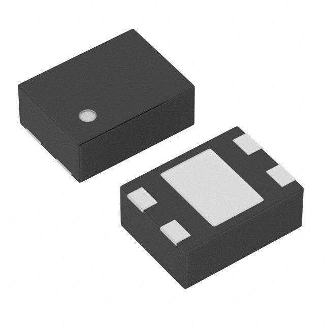
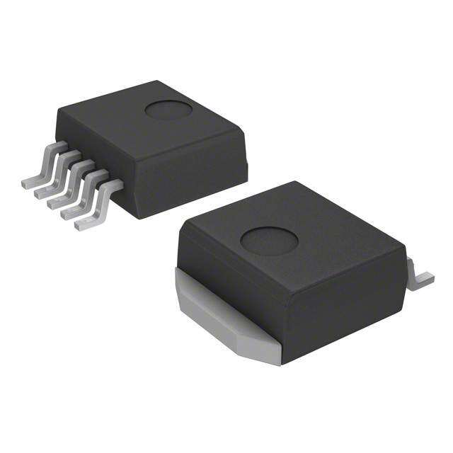
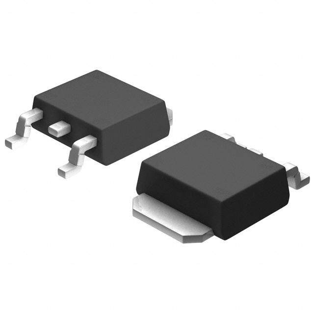
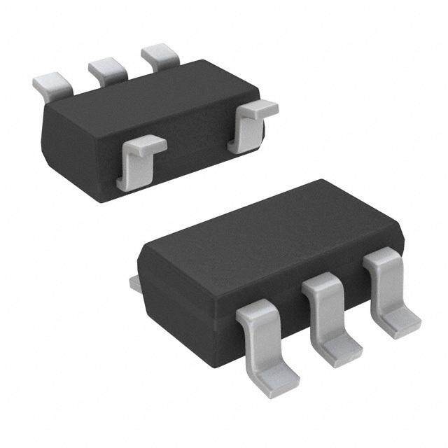
ICGOO在线商城 > 集成电路(IC) > PMIC - 稳压器 - 线性 > LDFM50PT-TR
- 型号: LDFM50PT-TR
- 制造商: STMicroelectronics
- 库位|库存: xxxx|xxxx
- 要求:
| 数量阶梯 | 香港交货 | 国内含税 |
| +xxxx | $xxxx | ¥xxxx |
查看当月历史价格
查看今年历史价格
LDFM50PT-TR产品简介:
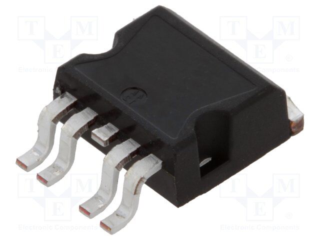
ICGOO电子元器件商城为您提供LDFM50PT-TR由STMicroelectronics设计生产,在icgoo商城现货销售,并且可以通过原厂、代理商等渠道进行代购。 LDFM50PT-TR价格参考。STMicroelectronicsLDFM50PT-TR封装/规格:PMIC - 稳压器 - 线性, Linear Voltage Regulator IC 1 Output 500mA PPAK。您可以下载LDFM50PT-TR参考资料、Datasheet数据手册功能说明书,资料中有LDFM50PT-TR 详细功能的应用电路图电压和使用方法及教程。
| 参数 | 数值 |
| 产品目录 | 集成电路 (IC)半导体 |
| 描述 | IC REG LDO 5V 0.5A PPAK-5低压差稳压器 500mA drop VTG Reg |
| 产品分类 | |
| 品牌 | STMicroelectronics |
| 产品手册 | |
| 产品图片 |
|
| rohs | 符合RoHS无铅 / 符合限制有害物质指令(RoHS)规范要求 |
| 产品系列 | 电源管理 IC,低压差稳压器,STMicroelectronics LDFM50PT-TR- |
| mouser_ship_limit | 该产品可能需要其他文件才能进口到中国。 |
| 数据手册 | |
| 产品型号 | LDFM50PT-TR |
| PSRR/纹波抑制—典型值 | 60 dB |
| 产品 | LDO Regulators |
| 产品种类 | 低压差稳压器 |
| 供应商器件封装 | PPAK |
| 其它名称 | 497-14186-6 |
| 包装 | Digi-Reel® |
| 参考电压 | 0.8 V |
| 商标 | STMicroelectronics |
| 回动电压—最大值 | 300 mV |
| 安装类型 | 表面贴装 |
| 安装风格 | SMD/SMT |
| 封装 | Reel |
| 封装/外壳 | TO-252-5,DPak(4 引线 + 接片),TO-252AD |
| 封装/箱体 | PPAK-5 |
| 工作温度 | -40°C ~ 125°C |
| 工厂包装数量 | 2500 |
| 最大功率耗散 | Internally Limited |
| 最大工作温度 | + 125 C |
| 最大输入电压 | 16 V |
| 最小工作温度 | + 40 C |
| 最小输入电压 | 2.5 V |
| 标准包装 | 1 |
| 电压-跌落(典型值) | 0.125V @ 500mA |
| 电压-输入 | 最高 16V |
| 电压-输出 | 5V |
| 电压调节准确度 | 1 % |
| 电流-输出 | 500mA |
| 电流-限制(最小值) | - |
| 电源电流 | 200 uA |
| 稳压器拓扑 | 正,固定式 |
| 稳压器数 | 1 |
| 类型 | Low Drop Voltage |
| 系列 | LDFM |
| 线路调整率 | 0.01 % / V |
| 负载调节 | 0.1 % / A |
| 输出电压 | 5 V |
| 输出电流 | 500 mA |
| 输出端数量 | 1 Output |
| 输出类型 | Fixed |



PDF Datasheet 数据手册内容提取
LDFM 500 mA very low drop voltage regulator Datasheet - production data Applications PCs and laptop computers Battery-powered equipment Industrial and medical equipment Portable equipment Description The LDFM is a fast, very low drop linear regulator which operates from an input supply voltage in the range of 2.5 V to 16 V. It is available in fixed and adjustable output voltage versions, from 0.8 V to 12 V. The LDFM features high output precision, very Features low dropout voltage, low noise, and low quiescent Input voltage from 2.5 to 16 V current, therefore suitable for low voltage Very low dropout voltage (300 mV max. at microprocessors and memory applications. 500 mA load) Enable logic control pin and Power Good output Low quiescent current (200 µA typ. @ are featured on PPAK/DFN packages. 500 mA load) Available in 1 % precision in PPAK and Current and thermal protection are provided. DFN6 packages, 2 % in DPAK 500 mA guaranteed output current Wide range of output voltages available on request: adjustable from 0.8 V, fixed up to 12 V in 100 mV steps Logic-controlled electronic shutdown Power Good (PPAK and DFN packages) Fast dynamic response to line and load changes Internal current and thermal protection Temperature range: - 40 °C to 125 °C July 2017 DocID023585 Rev 5 1/36 This is information on a product in full production. www.st.com
Contents LDFM Contents 1 Block diagram .................................................................................. 3 2 Pin configuration ............................................................................. 4 3 Typical application .......................................................................... 5 4 Absolute maximum ratings ............................................................. 6 5 Electrical characteristics ................................................................ 7 6 Application information ................................................................ 11 6.1 External capacitors .......................................................................... 11 6.1.1 Input capacitor .................................................................................. 11 6.1.2 Output capacitor ............................................................................... 11 6.2 Enable pin operation ....................................................................... 11 6.3 Power Good .................................................................................... 11 7 Typical performance characteristics ........................................... 12 8 Package information ..................................................................... 16 8.1 PPAK package information ............................................................. 17 8.2 PPAK packing information .............................................................. 19 8.3 DPAK (TO-252) package information .............................................. 21 8.4 DPAK (TO-252) packing information .............................................. 24 8.5 DFN6 (2x2) package information .................................................... 26 8.6 DFN6 (2x2) packing information ...................................................... 29 8.7 DFN6 (3x3) package information .................................................... 30 8.8 DFN6 (3x3) packing information ...................................................... 32 9 Ordering information ..................................................................... 34 10 Revision history ............................................................................ 35 2/36 DocID023585 Rev 5
LDFM Block diagram 1 Block diagram Figure 1: Block diagram (generic version) DocID023585 Rev 5 3/36
Pin configuration LDFM 2 Pin configuration Figure 2: Pin connection (top view) Table 1: Pin description DPAK, PPAK Pin n° Symbol Function PPAK DPAK For adjustable versions: error amplifier input pin. 5 - ADJ/PG For fixed version: Power Good output 2 1 VIN Input voltage 4 3 VOUT Output voltage 1 - EN Enable pin logic input: Low = shutdown, High = active 3 2 GND Ground TAB TAB GND Ground Table 2: Pin description DFN6-2x2 and 3x3 Pin n° Symbol Function For adjustable versions: error amplifier input pin. For fixed 2 ADJ/NC version: not connected 6 VIN Input voltage 1 VOUT Output Voltage 5 EN Enable pin logic input: low = shutdown, high = active 3 PG Power good output 4 GND Ground exposed pad GND Ground 4/36 DocID023585 Rev 5
LDFM Typical application 3 Typical application Figure 3: Fixed versions Figure 4: Adjustable version (PPAK and DFN6 packages only) DocID023585 Rev 5 5/36
Absolute maximum ratings LDFM 4 Absolute maximum ratings Table 3: Absolute maximum ratings Symbol Parameter Value Unit VIN DC input voltage - 0.3 to 20 V VOUT DC output voltage - 0.3 to VIN + 0.3 V VEN Enable input voltage - 0.3 to VIN + 0.3 V VADJ Adjust pin voltage - 0.3 to 2 V VPG Power Good pin voltage - 0.3 to VIN + 0.3 V ILOAD Output current Internally limited mA PD Power dissipation Internally limited mW TSTG Storage temperature range - 65 to 150 °C TOP Operating junction temperature range - 40 to 125 °C Absolute maximum ratings are those values beyond which damage to the device may occur. Functional operation under these conditions is not implied. All values are referred to GND. Table 4: Thermal data Value Symbol Parameter Unit PPAK DPAK DFN6-2x2 DFN6-3x3 RthJA Thermal resistance junction-ambient 100 100 65 55 °C/W RthJC Thermal resistance junction-case 8 8 6.5 10 °C/W 6/36 DocID023585 Rev 5
LDFM Electrical characteristics 5 Electrical characteristics T = 25 °C, V = V + 1 Va, C = 1 µF, C = 2.2 µF, I = 10 mA, V = 2 V, J IN OUT(NOM) IN OUT LOAD EN unless otherwise specified. Table 5: Electrical characteristics for LDFM (fixed versions) Symbol Parameter Test conditions Min. Typ. Max. Unit VIN Operating input voltage 2.5 16 V VOUT+1 V≤ VIN≤ 16 V (1) -1 1 % VOUT accuracy, ILOAD = 10 mA VOUT PPAK and DFN6 versions 10 mA ≤ ILOAD≤ 500 mA -1.5 1.5 % TJ = -40 to 125 °C VOUT+1 V(1) ≤ VIN ≤ 16 V -2 2 % VOUT accuracy, ILOAD = 10 mA VOUT DPAK version 10 mA ≤ ILOAD ≤ 500 mA -3 3 % TJ = -40 to 125 °C VOUT+1 V(1) ≤ VIN ≤ 16 V 0.01 ∆VOUT Static line regulation VOUT+1 V(1) ≤ VIN ≤ 16 V, %/V 0.04 TJ = -40 to 125 °C 10 mA ≤ ILOAD ≤ 500 mA 0.1 10 mA ≤ ILOAD ≤ 500 mA, %/A 0.15 0.4 TJ = -40 to 125 °C ∆VOUT Static load regulation 10 mA ≤ ILOAD ≤ 500 mA, TJ = -40 to 125 °C 10 mV DFN6 version VDROP Dropout voltage (2) ILOAD = 500 mA, 125 300 mV -40 °C < TJ < 125 °C ON mode: VEN = 2 V ILOAD= 10 mA to 500 mA, 200 800 TJ = -40 to 125 °C OFF Mode: VEN = GND, IQ Quiescent current 30 µA PPAK and DFN versions OFF Mode: VEN = GND, PPAK and DFN versions, 120 -40 °C < TJ < 125 °C ISC Short-circuit current 0.8 A Enable input logic low VIN = 2.5 V to 16 V, 0.8 VEN V Enable input logic high -40 °C<TJ<125 °C 2 IEN Enable pin input current VEN = VIN 5 10 µA 0.92* PG Power Good output threshold Rising edge V VOUT a For VOUT < 1.5 V; VIN = 2.5 V. DocID023585 Rev 5 7/36
Electrical characteristics LDFM Symbol Parameter Test conditions Min. Typ. Max. Unit 0.8* Falling edge VOUT Power Good output voltage low ISINK = 6 mA, open drain output 0.4 VIN = 6 V +/- 0.5 VRIPPLE Freq. = 120 Hz, 60 VOUT = 5 V SVR Supply voltage rejection dB VIN = 6 V +/- 0.5 VRIPPLE Freq. = 10 kHz, 52 VOUT = 5 V Bw = 10 Hz to 100 kHz, eN Output noise voltage ILOAD = 100 mA 45 µVRMS/VOUT COUT = 2.2 µF Thermal shutdown 170 TSHDN °C Hysteresis 10 Notes: (1)For VOUT < 1.5 V; VIN = 2.5 V. (2)Dropout voltage is the input-to-output voltage difference at which the output voltage is 100 mV below its nominal value. This specification does not apply for output voltages below 1.5 V. 8/36 DocID023585 Rev 5
LDFM Electrical characteristics T = 25 °C, V = V + 1 Va, C = 1 µF, C = 2.2 µF, I = 10 mA, V = 2 V, J IN OUT(NOM) IN OUT LOAD EN unless otherwise specified. Table 6: Electrical characteristics for LDFM (adjustable version) Symbol Parameter Test conditions Min. Typ. Max. Unit VIN Operating input voltage 2.5 16 V Reference voltage VIN = VOUT+1 V (1) 0.8 V VOUT+1 V(1) ≤ VIN ≤ 16 V -1 1 VADJ ILOAD = 10 mA Reference voltage tolerance % 10 mA ≤ ILOAD ≤ 500 mA -1.5 1.5 TJ = -40 to 125 °C VOUT+1 V (1) ≤ VIN ≤ 16 V 0.01 ∆VOUT Static line regulation VOUT+1 V(1) ≤ VIN ≤ 16 V, %/V 0.04 TJ = -40 to 125 °C 10 mA ≤ ILOAD ≤ 500 mA 0.06 10 mA ≤ ILOAD ≤ 500 mA, %/A 0.2 0.4 TJ = -40 to 125 °C ∆VOUT Static load regulation 10 mA ≤ ILOAD ≤ 500 mA, TJ = -40 to 125 °C 10 DFN6 version VOUT fixed to 2.5 V, VDROP Dropout voltage (2) ILOAD = 500 mA, 125 300 mV -40 °C < TJ < 125 °C ON mode: VEN = 2 V ILOAD= 10 mA to 500 mA, 200 800 TJ = -40 to 125 °C OFF Mode: VEN = GND, IQ Quiescent current 30 µA PPAK and DFN versions OFF Mode: VEN = GND, PPAK and DFN versions, 120 -40 °C < TJ < 125 °C ISC Short-circuit current 0.8 A Enable input logic low VIN= 2.5 V to 16 V, 0.8 VEN V Enable input logic high -40 °C < TJ < 125 °C 2 IEN Enable pin input current VEN = VIN 5 10 µA 0.92* Rising edge VADJ Power Good output threshold 0.8* PG Falling edge V VADJ ISINK = 6 mA, Power Good output voltage low 0.4 open drain output a For VOUT < 1.5 V; VIN = 2.5 V. DocID023585 Rev 5 9/36
Electrical characteristics LDFM Symbol Parameter Test conditions Min. Typ. Max. Unit VIN = VOUT+1 V +/- 0.5 VRIPPLE Freq. = 120 Hz, 62 VOUT = 0.8 V SVR Supply voltage rejection dB VIN = VOUT+1 V +/- 0.5 VRIPPLE Freq. = 10 kHz, 55 VOUT = 0.8 V Bw = 10 Hz to 100 kHz, eN Output noise voltage ILOAD = 100 mA 50 µVRMS/VOUT COUT = 2.2 µF Thermal shutdown 170 TSHDN °C Hysteresis 10 Notes: (1)For VOUT < 1.5 V; VIN = 2.5 V. (2)Dropout voltage is the input-to-output voltage difference at which the output voltage is 100 mV below its nominal value. This specification does not apply for output voltages below 1.5 V. 10/36 DocID023585 Rev 5
LDFM Application information 6 Application information 6.1 External capacitors The LDFM requires external capacitors for regulator stability. These capacitors must be selected to meet the requirements of minimum capacitance and equivalent series resistance (see Figure 25: "Stability plane adj (C , ESR)" and Figure 26: "Stability plane OUT 3.3 V(C , ESR)"). It is advisable to locate the input/output capacitors as close as possible OUT to the relative pins. 6.1.1 Input capacitor An input capacitor with a minimum value of 1 µF is required with the LDFM. This capacitor must be located a distance of not more than 0.5" from the input pin of the device and returned to a clean analog ground. Any good quality ceramic capacitors can be used for this capacitor. 6.1.2 Output capacitor It is possible to use ceramic capacitors but the output capacitor must meet the requirements for minimum amount of capacitance and E.S.R. (equivalent series resistance) value. A minimum capacitance of 2.2 µF is a good choice to guarantee the stability of the regulator. However, other C values can be used according to Figure 25: "Stability plane OUT adj (C , ESR)" and Figure 26: "Stability plane 3.3 V (C , ESR)", showing the allowable OUT OUT ESR range as a function of the output capacitance. The output capacitor must maintain its ESR in the stable region over the full operating temperature range to assure stability. Also, capacitor tolerance and variation with temperature must be kept in consideration in order to assure the minimum amount of capacitance at all times. 6.2 Enable pin operation The Enable pin can be used to turn OFF the regulator when pulled down, so drastically reducing the current consumption. When the enable feature is not used, this pin must be tied to V to keep the regulator output ON at all times. To assure proper operation, the IN signal source used to drive the Enable pin must be able to swing above and below the specified thresholds listed in the electrical characteristics section (V ). The Enable pin EN must not be left floating because it is not internally pulled down/up. 6.3 Power Good The LDFM features an open drain Power Good (PG) pin to sequence external supplies or loads and to provide fault detection. This pin requires an external resistor (R ) to pull PG PG high when the output is within the PG tolerance window. Typical values for this resistor range from 10 kΩ to 100 kΩ. DocID023585 Rev 5 11/36
Typical performance characteristics LDFM 7 Typical performance characteristics C = C = 1 µF, V = V +1 V, V to V I = 10 mA, unless otherwise specified. IN OUT IN OUT EN IN, OUT Figure 6: Output voltage vs temperature for Figure 5: Output voltage vs temperature adjustable Figure 7: Line regulation vs temperature Figure 8: Load regulation vs temperature Figure 9: Short-circuit current vs drop voltage Figure 10: Dropout voltage vs temperature 12/36 DocID023585 Rev 5
LDFM Typical performance characteristics Figure 11: Quiescent current vs temperature Figure 12: Quiescent current vs temperature (IOUT = 10 mA) (IOUT = 500 mA) Figure 13: Shutdown current vs temperature Figure 14: Enable pin current vs temperature Figure 15: Enable high threshold vs temperature Figure 16: Enable low threshold vs temperature DocID023585 Rev 5 13/36
Typical performance characteristics LDFM Figure 17: Output voltage vs input voltage Figure 18: Line transient Figure 19: Load transient (VOUT = 3.3 V) Figure 20: Load transient (VOUT = VADJ) 14/36 DocID023585 Rev 5
LDFM Typical performance characteristics Figure 21: Startup transient Figure 22: Enable transient Figure 23: SVR vs frequency (VOUT = 5 V) Figure 24: SVR vs frequency (VOUT = VADJ) Figure 25: Stability plane adj (COUT, ESR) Figure 26: Stability plane 3.3 V (COUT, ESR) DocID023585 Rev 5 15/36
Package information LDFM 8 Package information In order to meet environmental requirements, ST offers these devices in different grades of ECOPACK® packages, depending on their level of environmental compliance. ECOPACK® specifications, grade definitions and product status are available at: www.st.com. ECOPACK® is an ST trademark. 16/36 DocID023585 Rev 5
LDFM Package information 8.1 PPAK package information Figure 27: PPAK package outline DocID023585 Rev 5 17/36
Package information LDFM Table 7: PPAK mechanical data mm Dim. Min. Typ. Max. A 2.2 2.4 A1 0.9 1.1 A2 0.03 0.23 B 0.4 0.6 B2 5.2 5.4 C 0.45 0.6 C2 0.48 0.6 D 6 6.2 D1 5.1 E 6.4 6.6 E1 4.7 e 1.27 G 4.9 5.25 G1 2.38 2.7 H 9.35 10.1 L2 0.8 1 L4 0.6 1 L5 1 L6 2.8 R 0.20 V2 0° 8° 18/36 DocID023585 Rev 5
LDFM Package information 8.2 PPAK packing information Figure 28: PPAK tape outline DocID023585 Rev 5 19/36
Package information LDFM Figure 29: PPAK reel outline Table 8: PPAK tape and reel mechanical data Tape Reel mm mm Dim. Dim. Min. Max. Min. Max. A0 6.8 7 A 330 B0 10.4 10.6 B 1.5 B1 12.1 C 12.8 13.2 D 1.5 1.6 D 20.2 D1 1.5 G 16.4 18.4 E 1.65 1.85 N 50 F 7.4 7.6 T 22.4 K0 2.55 2.75 P0 3.9 4.1 Base qty. 2500 P1 7.9 8.1 Bulk qty. 2500 P2 1.9 2.1 R 40 T 0.25 0.35 W 15.7 16.3 20/36 DocID023585 Rev 5
LDFM Package information 8.3 DPAK (TO-252) package information Figure 30: DPAK (TO-252) package outline DocID023585 Rev 5 21/36
Package information LDFM Table 9: DPAK (TO-252) mechanical data mm Dim. Min. Typ. Max. A 2.20 2.40 A1 0.90 1.10 A2 0.03 0.23 b 0.64 0.90 b4 5.20 5.40 c 0.45 0.60 c2 0.48 0.60 D 6.00 6.20 D1 5.10 E 6.40 6.60 E1 5.20 e 2.28 e1 4.40 4.60 H 9.35 10.10 L 1.00 1.50 (L1) 2.80 L2 0.80 L4 0.60 1.00 R 0.20 V2 0° 8° 22/36 DocID023585 Rev 5
LDFM Package information Figure 31: DPAK (TO-252) recommended footprint (dimensions are in mm) DocID023585 Rev 5 23/36
Package information LDFM 8.4 DPAK (TO-252) packing information Figure 32: DPAK (TO-252) tape outline 24/36 DocID023585 Rev 5
LDFM Package information Figure 33: DPAK (TO-252) reel outline Table 10: DPAK (TO-252) tape and reel mechanical data Tape Reel mm mm Dim. Dim. Min. Max. Min. Max. A0 6.8 7 A 330 B0 10.4 10.6 B 1.5 B1 12.1 C 12.8 13.2 D 1.5 1.6 D 20.2 D1 1.5 G 16.4 18.4 E 1.65 1.85 N 50 F 7.4 7.6 T 22.4 K0 2.55 2.75 P0 3.9 4.1 Base qty. 2500 P1 7.9 8.1 Bulk qty. 2500 P2 1.9 2.1 R 40 T 0.25 0.35 W 15.7 16.3 DocID023585 Rev 5 25/36
Package information LDFM 8.5 DFN6 (2x2) package information Figure 34: DFN6 (2x2) package outline 26/36 DocID023585 Rev 5
LDFM Package information Table 11: DFN6 (2x2) mechanical data mm Dim. Min. Typ. Max. A 0.80 0.90 1.00 A1 0.00 0.02 0.05 b 0.25 0.30 0.35 D 2.00 BSC E 2.00 BSC e 0.65 BSC D2 1.45 1.70 E2 0.85 1.10 L 0.20 0.30 K 0.15 aaa 0.05 bbb 0.10 ccc 0.10 ddd 0.05 eee 0.08 N 6 DocID023585 Rev 5 27/36
Package information LDFM Figure 35: DFN6 (2x2) recommended footprint 28/36 DocID023585 Rev 5
LDFM Package information 8.6 DFN6 (2x2) packing information Figure 36: DFN6 (2x2) reel outline Table 12: DFN6 (2x2) tape and reel mechanical data mm Dim. Min. Typ. Max. A 180 C 12.8 13.2 D 20.2 N 60 T 14.4 A0 2.4 B0 2.4 K0 1.3 P0 4 P 4 DocID023585 Rev 5 29/36
Package information LDFM 8.7 DFN6 (3x3) package information Figure 37: DFN6 (3x3) package outline 30/36 DocID023585 Rev 5
LDFM Package information Table 13: DFN6 (3x3) mechanical data mm Dim. Min. Typ. Max. A 0.80 1 A1 0 0.02 0.05 A3 0.20 b 0.23 0.45 D 2.90 3 3.10 D2 2.23 2.50 E 2.90 3 3.10 E2 1.50 1.75 e 0.95 L 0.30 0.40 0.50 Figure 38: DFN6 (3x3) recommended footprint DocID023585 Rev 5 31/36
Package information LDFM 8.8 DFN6 (3x3) packing information Figure 39: DFN6 (3x3) tape outline 32/36 DocID023585 Rev 5
LDFM Package information Figure 40: DFN6 (3x3) reel outline Table 14: DFN6 (3x3) tape and reel mechanical data mm Dim. Min. Typ. Max. A0 3.20 3.30 3.40 B0 3.20 3.30 3.40 K0 1 1.10 1.20 DocID023585 Rev 5 33/36
Ordering information LDFM 9 Ordering information Table 15: Order code DPAK PPAK DFN6-2x2 DFN6-3x3 Output voltage LDFM33DT-TR LDFM33PT-TR LDFM33PVR LDFM33PUR 3.3 V LDFM50DT-TR LDFM50PT-TR 5 V LDFMPT-TR LDFMPVR LDFMPUR ADJ from 0.8 V 34/36 DocID023585 Rev 5
LDFM Revision history 10 Revision history Table 16: Document revision history Date Revision Changes 28-Aug-2012 1 Initial release. Part numbers LDFM and LDFM50 have been unified under LDFM. Updated the Features and the Description in cover page. Cancelled Table1: Device summary. Updated Section 2: Pin configuration, Section 3: Typical application, Section 4: 22-Nov-2013 2 Absolute maximum ratings, Section 5: Electrical characteristics and Section 8: Package information. Added Section 8.7: DFN6 (3 x 3 mm) packing information and Section 9: Order code. Minor text changes. Updated Table 5: Electrical characteristics for LDFM (fixed versions) and Table 6: 15-Jun-2015 3 Electrical characteristics for LDFM (adjustable version). Minor text changes. Updated Section 9: "Ordering information". 05-Sep-2016 4 Minor text changes. Updated Section 9: "Ordering information". 05-Jul-2017 5 Minor text changes. DocID023585 Rev 5 35/36
LDFM IMPORTANT NOTICE – PLEASE READ CAREFULLY STMicroelectronics NV and its subsidiaries (“ST”) reserve the right to make changes, corrections, enhancements, modifications, and improvements to ST products and/or to this document at any time without notice. Purchasers should obtain the latest relevant information on ST products before placing orders. ST products are sold pursuant to ST’s terms and conditions of sale in place at the time of order acknowledgement. Purchasers are solely responsible for the choice, selection, and use of ST products and ST assumes no liability for application assistance or the design of Purchasers’ products. No license, express or implied, to any intellectual property right is granted by ST herein. Resale of ST products with provisions different from the information set forth herein shall void any warranty granted by ST for such product. ST and the ST logo are trademarks of ST. All other product or service names are the property of their respective owners. Information in this document supersedes and replaces information previously supplied in any prior versions of this document. © 2017 STMicroelectronics – All rights reserved 36/36 DocID023585 Rev 5
Mouser Electronics Authorized Distributor Click to View Pricing, Inventory, Delivery & Lifecycle Information: S TMicroelectronics: LDFM50DT-TR LDFM50PT-TR LDFMPT-TR LDFMPVR LDFMPUR LDFM33PUR LDFM33PVR
 Datasheet下载

