ICGOO在线商城 > 集成电路(IC) > PMIC - 稳压器 - 线性 > LD3985M33R
 Datasheet下载
- 型号: LD3985M33R
- 制造商: STMicroelectronics
- 库位|库存: xxxx|xxxx
- 要求:
| 数量阶梯 | 香港交货 | 国内含税 |
| +xxxx | $xxxx | ¥xxxx |
查看当月历史价格
查看今年历史价格
LD3985M33R产品简介:
ICGOO电子元器件商城为您提供LD3985M33R由STMicroelectronics设计生产,在icgoo商城现货销售,并且可以通过原厂、代理商等渠道进行代购。 LD3985M33R价格参考¥1.53-¥1.53。STMicroelectronicsLD3985M33R封装/规格:PMIC - 稳压器 - 线性, Linear Voltage Regulator IC 1 Output 150mA SOT-23-5。您可以下载LD3985M33R参考资料、Datasheet数据手册功能说明书,资料中有LD3985M33R 详细功能的应用电路图电压和使用方法及教程。
| 参数 | 数值 |
| 产品目录 | 集成电路 (IC)半导体 |
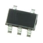
| 描述 | IC REG LDO 3.3V 0.15A SOT23-5低压差稳压器 BICMOS VOLT REG |
| 产品分类 | |
| 品牌 | STMicroelectronics |
| 产品手册 | |
| 产品图片 |
|
| rohs | 符合RoHS无铅 / 符合限制有害物质指令(RoHS)规范要求 |
| 产品系列 | 电源管理 IC,低压差稳压器,STMicroelectronics LD3985M33R- |
| 数据手册 | |
| 产品型号 | LD3985M33R |
| 产品目录页面 | |
| 产品种类 | 低压差稳压器 |
| 供应商器件封装 | SOT-23-5 |
| 其它名称 | 497-3504-2 |
| 其它有关文件 | http://www.st.com/web/catalog/sense_power/FM142/CL1015/SC312/SS1732/PF69230?referrer=70071840http://www.st.com/web/catalog/sense_power/FM142/CL1015/SC312/SS1733/PF69230?referrer=70071840 |
| 包装 | 带卷 (TR) |
| 商标 | STMicroelectronics |
| 安装类型 | 表面贴装 |
| 安装风格 | SMD/SMT |
| 封装 | Reel |
| 封装/外壳 | SC-74A,SOT-753 |
| 封装/箱体 | SOT-23 |
| 工作温度 | -40°C ~ 125°C |
| 工厂包装数量 | 3000 |
| 最大工作温度 | + 125 C |
| 最大输入电压 | 6 V |
| 最小工作温度 | - 40 C |
| 最小输入电压 | + 2.5 V |
| 标准包装 | 3,000 |
| 电压-跌落(典型值) | 0.06V @ 150mA |
| 电压-输入 | 最高 6V |
| 电压-输出 | 3.3V |
| 电压调节准确度 | 2 % |
| 电流-输出 | 150mA |
| 电流-限制(最小值) | 300mA |
| 稳压器拓扑 | 正,固定式 |
| 稳压器数 | 1 |
| 系列 | LD3985M |
| 线路调整率 | 0.1 % / V |
| 负载调节 | 0.005 % / mA |
| 输入偏压电流—最大 | 0.085 mA |
| 输出电压 | 3.3 V |
| 输出电流 | 150 mA |
| 输出端数量 | 1 Output |
| 输出类型 | Fixed |


- 商务部:美国ITC正式对集成电路等产品启动337调查
- 曝三星4nm工艺存在良率问题 高通将骁龙8 Gen1或转产台积电
- 太阳诱电将投资9.5亿元在常州建新厂生产MLCC 预计2023年完工
- 英特尔发布欧洲新工厂建设计划 深化IDM 2.0 战略
- 台积电先进制程称霸业界 有大客户加持明年业绩稳了
- 达到5530亿美元!SIA预计今年全球半导体销售额将创下新高
- 英特尔拟将自动驾驶子公司Mobileye上市 估值或超500亿美元
- 三星加码芯片和SET,合并消费电子和移动部门,撤换高东真等 CEO
- 三星电子宣布重大人事变动 还合并消费电子和移动部门
- 海关总署:前11个月进口集成电路产品价值2.52万亿元 增长14.8%


PDF Datasheet 数据手册内容提取
LD3985 Ultra low drop and low noise BiCMOS voltage regulators Datasheet - production data Power supply rejection is better than 60 dB at low frequencies and rolls off at 10 kHz. High power supply rejection is maintained down to low input voltage levels common to battery operated circuits. Shutdown logic control function is available, this means that when the device is used as local regulator, it is possible to put a part of the board in standby, decreasing the total power consumption. The LD3985 is designed to (cid:54)(cid:50)(cid:55)(cid:21)(cid:22)(cid:16)(cid:24)(cid:47) work with low ESR ceramic capacitors. Typical applications are in mobile phones and similar battery-powered wireless systems. Features • Input voltage from 2.5 V to 6 V • Stable with low ESR ceramic capacitors • Ultra low-dropout voltage (60 mV typ. at 150 mA load, 0.4 mV typ. at 1 mA load) • Very low quiescent current (85 µA typ. at no load, 170 µA typ. at 150 mA load; max.1.5 µA in OFF mode) • Guaranteed output current up to 150 mA • Wide range of output voltages: 1.22 V; 1.8 V; 2.5 V; 2.7 V; 2.8 V; 2.9 V; 3 V; 3.3 V; 4.7 V • Fast turn-on time: typ. 200 µs [C = 1 µF, O C = 10 nF and I = 1 mA] BYP O • Logic-controlled electronic shutdown • Internal current and thermal limit • Output low noise voltage 30 µV over 10 Hz RMS to 100 kHz • SVR of 60 dB at 1 kHz, 50 dB at 10 kHz • Temperature range: - 40 °C to 125 °C Description The LD3985 provides up to 150 mA, from 2.5 V to 6 V input voltage. The ultra low drop voltage, low quiescent current and low noise make it suitable for low power applications and in battery-powered systems. Regulator ground current increases slightly in dropout only, prolonging the battery life. July 2017 DocID9587 Rev 16 1/18 This is information on a product in full production. www.st.com
Contents LD3985 Contents 1 Diagram . . . . . . . . . . . . . . . . . . . . . . . . . . . . . . . . . . . . . . . . . . . . . . . . . . . 3 2 Pin configuration . . . . . . . . . . . . . . . . . . . . . . . . . . . . . . . . . . . . . . . . . . . . 4 3 Typical application . . . . . . . . . . . . . . . . . . . . . . . . . . . . . . . . . . . . . . . . . . 5 4 Maximum ratings . . . . . . . . . . . . . . . . . . . . . . . . . . . . . . . . . . . . . . . . . . . . 6 5 Electrical characteristics . . . . . . . . . . . . . . . . . . . . . . . . . . . . . . . . . . . . . 7 6 Typical performance characteristics . . . . . . . . . . . . . . . . . . . . . . . . . . . . 9 7 Package information . . . . . . . . . . . . . . . . . . . . . . . . . . . . . . . . . . . . . . . . 13 7.1 SOT23-5L package information . . . . . . . . . . . . . . . . . . . . . . . . . . . . . . . . 13 7.2 SOT23-5L packing information . . . . . . . . . . . . . . . . . . . . . . . . . . . . . . . . . 15 8 Ordering information . . . . . . . . . . . . . . . . . . . . . . . . . . . . . . . . . . . . . . . 16 9 Revision history . . . . . . . . . . . . . . . . . . . . . . . . . . . . . . . . . . . . . . . . . . . 17 2/18 DocID9587 Rev 16
LD3985 Diagram 1 Diagram Figure 1. Schematic diagram DocID9587 Rev 16 3/18 18
Pin configuration LD3985 2 Pin configuration Figure 2. Pin connection (top view) Table 1. Pin description Pin Symbol Name and function 1 V Input voltage of the LDO I 2 GND Common ground Inhibit input voltage: ON mode when V ≥ 1.2 V, OFF mode when V 3 V INH INH INH ≤ 0.4 V (Do not leave it floating, not internally pulled down/up) Bypass pin: an external capacitor (usually 10 nF) has to be connected to 4 BYPASS minimize noise voltage 5 V Output voltage of the LDO O 4/18 DocID9587 Rev 16
LD3985 Typical application 3 Typical application Figure 3. Typical application circuit DocID9587 Rev 16 5/18 18
Maximum ratings LD3985 4 Maximum ratings Table 2. Absolute maximum ratings Symbol Parameter Value Unit V DC input voltage -0.3 to 6 (1) V I V DC output voltage -0.3 to V+0.3 V O I V Inhibit input voltage -0.3 to V+0.3 V INH I I Output current Internally limited O P Power dissipation Internally limited D T Storage temperature range -65 to 150 °C STG T Operating junction temperature range -40 to 125 °C OP 1. The input pin is able to withstand non repetitive spike of 6.5 V for 200 ms. Note: Absolute maximum ratings are those values beyond which damage to the device may occur. Functional operation under these conditions is not implied. Table 3. Thermal data Symbol Parameter Value Unit R Thermal resistance junction-case 81 °C/W thJC R Thermal resistance junction-ambient 255 °C/W thJA 6/18 DocID9587 Rev 16
LD3985 Electrical characteristics 5 Electrical characteristics T = 25 °C, V = V +0.5 V, C = 1 µF, C = 10 nF, I = 1 mA, V = 1.4 V, unless J I O(NOM) I BYP O INH otherwise specified. Table 4. Electrical characteristics Symbol Parameter Test conditions Min. Typ. Max. Unit Operating input V 2.5 6 V I voltage Output voltage I = 1 mA -50 50 O V accuracy, V < mV O O(NOM) 2.5 V TJ = -40 to 125 °C -75 75 Output voltage I = 1 mA -2 2 O % of V accuracy, V ≥ O 2.5V O(NOM) TJ= -40 to 125 °C -3 3 VO(NOM) V = V + 0.5 I O(NOM) to 6 V -0.1 0.1 ΔV Line regulation (1) %/V O T = -40 to 125 °C J V = 4.7 to 5 V -0.19 0.19 O(NOM) I = 1 mA to 150 O mA, V < 2.5 ΔV Load regulation O(NOM) 0.002 0.008 %/mA O V T = -40 to 125 °C J I = 1 mA to 150 O mA, V ≥ 2.5 0.0004 0.002 O(NOM) V ΔVO Load regulation IO = 1 mA to %/mA 150mA, T = -40 to J 0.0025 0.005 125 °C, V ≥ O(NOM) 2.5 V V = V + 1 V, Output AC line I O(NOM) ΔVO regulation (2) IO = 150 mA, 1.5 mVPP t = t = 30 µs R F I = 0 85 O I = 0, T = -40 to Quiescent current O J 150 125 °C ON mode: V = INH I = 0 to 150 mA 170 1.2 V O I µA Q I = 0 to 150 mA, O 250 T = -40 to 125 °C J OFF mode: 0.003 VINH = 0.4 V TJ= -40 to 125 °C 1.5 DocID9587 Rev 16 7/18 18
Electrical characteristics LD3985 Table 4. Electrical characteristics (continued) Symbol Parameter Test conditions Min. Typ. Max. Unit I = 1 mA 0.4 O I = 1 mA, O 2 T = -40 to 125 °C J I = 50 mA 20 O I = 50 mA, O 35 T = -40 to 125 °C V Dropout voltage (3) J mV DROP I = 100 mA 45 O I = 100 mA, O 70 T = -40 to 125 °C J I = 150 mA 60 O I = 150 mA, O 100 T = -40 to 125 °C J I Short-circuit current R = 0 600 mA SC L V = f = 1 I 60 V +0.2 kHz O(NOM) 5 V ± Supply voltage SVR rejection VRIPPLE = 0.1 f = dB V, IO= 50 mA 10 50 VO(NOM) < 2.5 kHz V, V = 2.55 V I I Peak output current V ≥ V - 5% 300 550 mA O(PK) O O(NOM) Inhibit input logic 0.4 low V = 2.5 V to 6 V, V I V INH Inhibit input logic TJ= -40 to 125 °C 1.2 high V = 0.4 V, I Inhibit input current INH ±1 nA INH V = 6 V I B = 10 Hz to 100 eN Output noise voltage W 30 µV kHz, C = 1 µF RMS O t Turn-on time (4) C = 10 nF 100 250 µs ON BYP T Thermal shutdown (5) 160 °C SHDN Capacitance (6) 1 22 µF C Output capacitor O ESR 5 5000 mΩ 1. For V < 2 V, V = 2.5 V O(NOM) I 2. For V = 1.25 V, V = 2.5 V O(NOM) I 3. Dropout voltage is the input-to-output voltage difference at which the output voltage is 100 mV below its nominal value. This specification does not apply to input voltages below 2.5 V 4. Turn-on time is time measured between the enable input just exceeding V high value and the output INH voltage just reaching 95% of its nominal value 5. Typical thermal protection hysteresis is 20 °C 6. The minimum capacitor value is 1 µF, anyway the LD3985 is still stable if the compensation capacitor has a 30% tolerance in all temperature range 8/18 DocID9587 Rev 16
LD3985 Typical performance characteristics 6 Typical performance characteristics T = 25 °C, V = V +0.5 V, C = C = 1 µF, C = 10 nF, I = 1 mA, V = 1.4 V, J I O(NOM) I O BYP O INH unless otherwise specified. Figure 4. Output voltage vs. temperature Figure 5. Output voltage vs. temperature (V =1.35 V) (V =2.7 V) 0 0 Figure 6. Output voltage vs. temperature Figure 7. Shutdown voltage vs. temperature (V =3.3 V) (V =1.35 V) 0 0 DocID9587 Rev 16 9/18 18
Typical performance characteristics LD3985 Figure 8. Shutdown voltage vs. temperature Figure 9. Line regulation vs. temperature (V =3.3 V) (V =1.35 V) 0 0 Figure 10 . Line regulation vs. temperature Figure 11. Line regulation vs. temperature (V =2.7 V) (V =3.3 V) 0 0 Figure 12. Load regulation vs. temperature Figure 13. Load regulation vs. temperature (V =1.35 V) (V =2.7 V) 0 0 10/18 DocID9587 Rev 16
LD3985 Typical performance characteristics Figure 14. Load regulation vs. temperature Figure 15. Quiescent current vs. temperature (V =3.3 V) (V=2.5 V) 0 I Figure 16. Q uiescent current vs. temperature Figure 17. Quiescent current vs. load current (V=6 V) I Figure 18. Supply voltage rejection vs. Figure 19. Load transient response frequency V = 3.2 V, I = 1 to 150 mA, rise-fall time= 1 µs I O DocID9587 Rev 16 11/18 18
Typical performance characteristics LD3985 Figure 20. Line transient response Figure 21. Startup V = 3.8 V to 4.4 V, T = 25 °C, I = 150 mA, C = C V = 3.3 V, I = 1 mA, C = C = 1 µF (cer), C = I J O I O I O I O BYP = 1 µF (X7R), C = 10 nF, rise-fall time= 1 µs, 10 nF, T = 20 ns, V = 2.8 V BYP r O V = 2.7 V O Figure 22. Turn-off V = 3.3 V, I = 1 mA, C = C = 1 mF (cer), C = I O I O BYP 10 nF, T = 20 ns, V = 2.8 V f O 12/18 DocID9587 Rev 16
LD3985 Package information 7 Package information In order to meet environmental requirements, ST offers these devices in different grades of ECOPACK® packages, depending on their level of environmental compliance. ECOPACK® specifications, grade definitions and product status are available at: www.st.com. ECOPACK® is an ST trademark. 7.1 SOT23-5L package information Figure 23. SOT23-5L package outline (cid:26)(cid:19)(cid:23)(cid:28)(cid:25)(cid:26)(cid:25)(cid:66)(cid:78) DocID9587 Rev 16 13/18 18
Package information LD3985 Table 5. SOT23-5L package mechanical data mm Dim. Min. Typ. Max. A 0.90 1.45 A1 0 0.15 A2 0.90 1.30 b 0.30 0.50 c 2.09 0.20 D 2.95 E 1.60 e 0.95 H 2.80 L 0.30 0.60 θ 0 8 Figure 24. SOT23-5L recommended footprint (dimensions in mm) (cid:26)(cid:19)(cid:23)(cid:28)(cid:25)(cid:26)(cid:25)(cid:66)(cid:78) 14/18 DocID9587 Rev 16
LD3985 Package information 7.2 SOT23-5L packing information Figure 25. SOT23-5L tape and reel outline Table 6. SOT23-5L tape and reel mechanical data mm Dim. Min. Typ. Max. A 180 C 12.8 13.0 13.2 D 20.2 N 60 T 14.4 Ao 3.13 3.23 3.33 Bo 3.07 3.17 3.27 Ko 1.27 1.37 1.47 Po 3.9 4.0 4.1 P 3.9 4.0 4.1 DocID9587 Rev 16 15/18 18
Ordering information LD3985 8 Ordering information Table 7. Ordering information Order code Output voltage LD3985M122R 1.22 V LD3985M18R 1.8 V LD3985M25R 2.5 V LD3985M27R 2.7 V LD3985M28R 2.8 V LD3985M29R 2.9 V LD3985M30R 3.0 V LD3985M33R 3.3 V LD3985M47R 4.7 V 16/18 DocID9587 Rev 16
LD3985 Revision history 9 Revision history Table 8. Document revision history Date Revision Changes 07-May-2004 6 Part number status changed on table 3. 05-Oct-2004 7 t values are changed on table 5. ON 27-Oct-2004 8 Order codes changed - table 3. 17-Mar-2005 9 Improved drawing quality for figures 19 - 20 - 21 - 22. 10-Apr-2007 10 Order codes updated. 08-Jun-2007 11 Order code change. 20-Dec-2007 12 Modified: Table1, Table12, mechanical data for Flip-chip. 02-Dec-2008 13 Modified: Table6 on page14 and Figure23 on page17. 03-Jan-2011 14 Modified: Features on page1 and Table12 on page20. Part number LD3985XX changed to LD3985. Modified title in cover page. 08-Jan-2014 15 Updated the description and Section7: Package mechanical data. Added Section8: Packaging mechanical data. Minor text changes. Removed Flip Chip (1.57x1.22) and TSOT23-5L package information. 20-Jul-2017 16 Removed device summary table. Updated the whole document accordingly. DocID9587 Rev 16 17/18 18
LD3985 IMPORTANT NOTICE – PLEASE READ CAREFULLY STMicroelectronics NV and its subsidiaries (“ST”) reserve the right to make changes, corrections, enhancements, modifications, and improvements to ST products and/or to this document at any time without notice. Purchasers should obtain the latest relevant information on ST products before placing orders. ST products are sold pursuant to ST’s terms and conditions of sale in place at the time of order acknowledgement. Purchasers are solely responsible for the choice, selection, and use of ST products and ST assumes no liability for application assistance or the design of Purchasers’ products. No license, express or implied, to any intellectual property right is granted by ST herein. Resale of ST products with provisions different from the information set forth herein shall void any warranty granted by ST for such product. ST and the ST logo are trademarks of ST. All other product or service names are the property of their respective owners. Information in this document supersedes and replaces information previously supplied in any prior versions of this document. © 2017 STMicroelectronics – All rights reserved 18/18 DocID9587 Rev 16
Mouser Electronics Authorized Distributor Click to View Pricing, Inventory, Delivery & Lifecycle Information: S TMicroelectronics: LD3985J33R LD3985G27R LD3985J18R LD3985M18R LD3985J26R LD3985J28R LD3985J29R LD3985G18R LD3985G25R LD3985G33R LD3985M122R LD3985M27R LD3985M28R LD3985M29R LD3985M30R LD3985M33R LD3985M25R LD3985J25R LD3985M47R LD3985G30R LD3985G28R LD3985G47R