ICGOO在线商城 > 集成电路(IC) > PMIC - 稳压器 - 线性 > LD39300PT25-R

 Datasheet下载
- 型号: LD39300PT25-R
- 制造商: STMicroelectronics
- 库位|库存: xxxx|xxxx
- 要求:
| 数量阶梯 | 香港交货 | 国内含税 |
| +xxxx | $xxxx | ¥xxxx |
查看当月历史价格
查看今年历史价格
LD39300PT25-R产品简介:
ICGOO电子元器件商城为您提供LD39300PT25-R由STMicroelectronics设计生产,在icgoo商城现货销售,并且可以通过原厂、代理商等渠道进行代购。 LD39300PT25-R价格参考。STMicroelectronicsLD39300PT25-R封装/规格:PMIC - 稳压器 - 线性, Linear Voltage Regulator IC Positive Fixed 1 Output 2.5V 3A PPAK。您可以下载LD39300PT25-R参考资料、Datasheet数据手册功能说明书,资料中有LD39300PT25-R 详细功能的应用电路图电压和使用方法及教程。
| 参数 | 数值 |
| 产品目录 | 集成电路 (IC)半导体 |
| 描述 | IC REG LDO 2.5V 3A PPAK低压差稳压器 Bicmos Vltg Regulatr Ultra Lo Drop |
| 产品分类 | |
| 品牌 | STMicroelectronics |
| 产品手册 | |
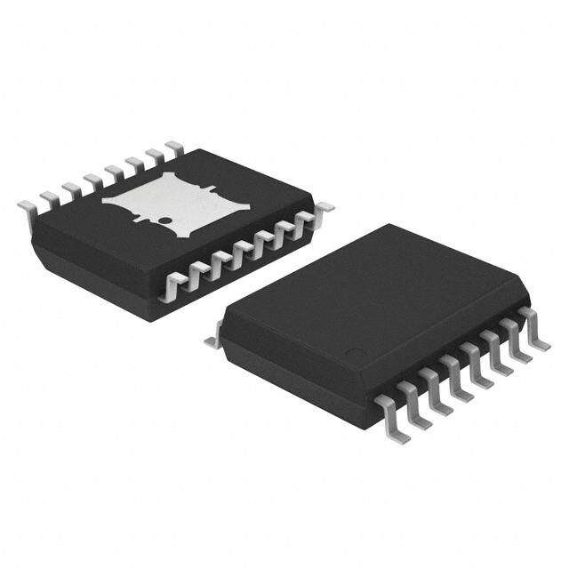
| 产品图片 |
|
| rohs | 符合RoHS无铅 / 符合限制有害物质指令(RoHS)规范要求 |
| 产品系列 | 电源管理 IC,低压差稳压器,STMicroelectronics LD39300PT25-R- |
| 数据手册 | |
| 产品型号 | LD39300PT25-R |
| 产品目录页面 | |
| 产品种类 | 低压差稳压器 |
| 供应商器件封装 | PPAK |
| 其它名称 | 497-6875-1 |
| 其它有关文件 | http://www.st.com/web/catalog/sense_power/FM142/CL1015/SC312/SS1733/PF157520?referrer=70071840 |
| 包装 | 剪切带 (CT) |
| 参考电压 | 1.22 V |
| 商标 | STMicroelectronics |
| 回动电压—最大值 | 80 mV at 600 mA |
| 安装类型 | 表面贴装 |
| 安装风格 | SMD/SMT |
| 封装 | Reel |
| 封装/外壳 | TO-252-5,DPak(4 引线 + 接片),TO-252AD |
| 封装/箱体 | PPAK-5 |
| 工作温度 | -40°C ~ 125°C |
| 工厂包装数量 | 2500 |
| 最大工作温度 | + 125 C |
| 最大输入电压 | 6 V |
| 最小工作温度 | - 40 C |
| 最小输入电压 | + 2.5 V |
| 标准包装 | 1 |
| 电压-跌落(典型值) | 0.2V @ 3A |
| 电压-输入 | 最高 6V |
| 电压-输出 | 2.5V |
| 电压调节准确度 | 1.5 % |
| 电流-输出 | 3A |
| 电流-限制(最小值) | - |
| 稳压器拓扑 | 正,固定式 |
| 稳压器数 | 1 |
| 系列 | LD39300XX25 |
| 线路调整率 | 0.04 % |
| 负载调节 | 0.06 % |
| 输入偏压电流—最大 | 1.2 mA |
| 输出电压 | 2.5 V |
| 输出电流 | 3 A |
| 输出端数量 | 1 Output |
| 输出类型 | Fixed |


- 商务部:美国ITC正式对集成电路等产品启动337调查
- 曝三星4nm工艺存在良率问题 高通将骁龙8 Gen1或转产台积电
- 太阳诱电将投资9.5亿元在常州建新厂生产MLCC 预计2023年完工
- 英特尔发布欧洲新工厂建设计划 深化IDM 2.0 战略
- 台积电先进制程称霸业界 有大客户加持明年业绩稳了
- 达到5530亿美元!SIA预计今年全球半导体销售额将创下新高
- 英特尔拟将自动驾驶子公司Mobileye上市 估值或超500亿美元
- 三星加码芯片和SET,合并消费电子和移动部门,撤换高东真等 CEO
- 三星电子宣布重大人事变动 还合并消费电子和移动部门
- 海关总署:前11个月进口集成电路产品价值2.52万亿元 增长14.8%


PDF Datasheet 数据手册内容提取
LD39300 Ultra low drop BICMOS voltage regulator Datasheet - production data Applications Microprocessor power supply DSPs power supply Post regulators for switching power supplies High efficiency linear regulator Description The LD39300 is a fast ultra low drop linear regulator which operates from 2.5 V to 6 V input supply. Features A wide range of output options are available. The 3 A guaranteed output current low drop voltage, low noise, and low quiescent Ultra low dropout voltage (200 mV typ. current make it suitable for low voltage @ 3 A load, 40 mV typ. @ 600 mA load) microprocessor and memory applications. The Very low quiescent current (1.2 mA typ. device is developed on a BiCMOS process which @ 3 A load, 1 µA max @ 25 °C in off mode) allows low quiescent current operation Logic-controlled electronic shutdown independently of output load current. Current and thermal internal limit ± 1.5 % output voltage tolerance @ 25 °C Fixed and ADJ output voltages: 1.22 V, ADJ Temperature range: -40 to 125 °C Fast dynamic response to line and load changes Stable with ceramic capacitor Available in PPAK and DPAK Table 1: Device summary Part number Output voltage DPAK PPAK LD39300DT12-R 1.22 V LD39300PT-R ADJ from 1.22 to 5.0 V March 2017 DocID13160 Rev 3 1/22 This is information on a product in full production. www.st.com
Contents LD39300 Contents 1 Diagram ............................................................................................ 3 2 Pin configuration ............................................................................. 4 3 Typical application circuits ............................................................. 5 4 Maximum ratings ............................................................................. 7 5 Electrical characteristics ................................................................ 8 6 Typical performance characteristics ........................................... 10 7 Application notes .......................................................................... 13 7.1 External capacitors .......................................................................... 13 7.2 Input capacitor ................................................................................. 13 7.3 Output capacitor .............................................................................. 13 7.4 Thermal note ................................................................................... 13 7.5 Inhibit input operation ...................................................................... 13 8 Package information ..................................................................... 14 8.1 DPAK package information ............................................................. 14 8.2 PPAK package information ............................................................. 17 8.3 PPAK and DPAK packing information ............................................. 19 9 Revision history ............................................................................ 21 2/22 DocID13160 Rev 3
LD39300 Diagram 1 Diagram Figure 1: Block diagram (*) Not present on ADJ versions. DocID13160 Rev 3 3/22
Pin configuration LD39300 2 Pin configuration Figure 2: Pin connections (top view for DPAK and PPAK) Table 2: Pin description Pin N° Symbol Note PPAK DPAK VSENSE/N.C. For fixed versions: Not connected on PPAK 5 ADJ For adjustable version: error amplifier Input pin for VO from 1.22 to 5.0 V 2 1 VI LnDotO m ionrpeu tth vaonlt a0g.5e’;’ fVroI fmro imnp 2u.t5 p Vin t.o 6 V, CI = 1 µF must be located at a distance of 4 3 VO LtoD COO o vust pEuSt Rvo slttaagbeili tpyi ncsh,a wrti)t h minimum CO = 4.7 µF needed for stability (also refer 1 VINH I(ndhoi bniot ti nlepauvt ev ofllotaagtien:g O, nNo Mt inOtDerEn awllhye pnu VlleINdH d≥o 2w nV/,u Op)F F MODE when VINH ≤ 0.3 V 3 2 GND Common ground TAB GND Tab is connected to GND 4/22 DocID13160 Rev 3
LD39300 Typical application circuits 3 Typical application circuits C and C capacitors must be placed as close as possible to the IC pins. I O Figure 3: LD39300 fixed version with inhibit Inhibit pin is not internally pulled down/up then it must not be left floating. It disables the device when connected to GND or to a positive voltage less than 0.3 V. Figure 4: LD39300 adjustable version Set R2 as close as possible to 4.7 KΩ. DocID13160 Rev 3 5/22
Typical application circuits LD39300 Figure 5: LD39300 DPAK Figure 6: Timing diagram 6/22 DocID13160 Rev 3
LD39300 Maximum ratings 4 Maximum ratings Table 3: Absolute maximum ratings Symbol Parameter Value Unit VI DC input voltage -0.3 to 6.5 V VINH INHIBIT input voltage -0.3 to VI + 0.3 (6.5 V max) V VO DC output voltage -0.3 to VI + 0.3 (6.5 V max) V VADJ ADJ pin voltage -0.3 to VI + 0.3 (6.5 V max) V IO Output current Internally limited mA PD Power dissipation Internally limited mW TSTG Storage temperature range -50 to 150 °C TOP Operating junction temperature range -40 to 125 °C Absolute maximum ratings are those values beyond which damage to the device may occur. Functional operation under these conditions is not implied. All values are referred to GND. Table 4: Thermal data Symbol Parameter PPAK DPAK Unit RthJA Thermal resistance junction-ambient 100 100 °C/W RthJC Thermal resistance junction-case 8 8 °C/W DocID13160 Rev 3 7/22
Electrical characteristics LD39300 5 Electrical characteristics T = 25 °C, V = V +1 V, C = 1 µF, C = 4.7 µF, I = 10 mA, V = 2 V, unless otherwise J I O I O LOAD INH specified. Table 5: Electrical characteristics Symbol Parameter Parameter Min. Typ. Max. Unit VI Operating input voltage 2.5 6 V VI = VO + 1 V, -1.5 1.5 ILOAD = 10 mA to 3 A VO Output voltage tolerance VI = VO + 1 V to 6 V, % of VO(NOM) ILOAD = 10 mA to 3 A -3 3 TJ = -40 to 125 °C VREF Reference voltage 1.22 V VI = VO + 1 V to 6 V 0.04 % ΔVO Output voltage LINE regulation VI = VO + 1 V to 6 V, 0.1 0.2 % TJ = -40 to 125 °C ILOAD = 10 mA to 3 A 0.06 ΔVO/ΔILOAD Output voltage LOAD regulation ILOAD = 10 mA to 3 A %/A 0.2 0.4 TJ = -40 to 125 °C ILOAD = 600 mA, 40 80 TJ= -40 to 125 °C VDROP Dropout voltage (VI - VO) mV ILOAD = 3 A, 200 400 TJ = -40 to 125 °C ILOAD = 10 mA to 3 A, Quiescent current: ON MODE VINH = 2 V 1.2 2.5 mA TJ = -40 to 125 °C IQ VINH = 0.3 V 1 Quiescent current: OFF MODE VINH = 0.3 V, µA 5 TJ = -40 to 125 °C Short-circuit protection ISC Short circuit protection RL = 0 6 A Inhibit input Inhibit threshold LOW VI = 2.5 to 6 V OFF 0.3 VINH V Inhibit threshold HIGH TJ = -40 to 125 °C 2 ILOAD = 3 A, TD-OFF Current limit 20 VO = 3.3 V µs ILOAD = 3 A, TD-ON Current limit 20 VO = 3.3 V IINH Inhibit input current (1) VI = 6 V, ±0.1 ±1 µA VINH = 0 to 6 V 8/22 DocID13160 Rev 3
LD39300 Electrical characteristics Symbol Parameter Parameter Min. Typ. Max. Unit AC parameters VI = 4.5 ± 1 V, f = 120 Hz 65 SVR Supply voltage rejection VO = 3.3 V, dB f = 1 kHz 55 ILOAD = 10 mA BW = 10 Hz to 100 kHz, eN Output noise voltage CO = 4.7 µF, 100 µVRMS VO = 2.5 V Thermal shutdown OFF 170 TSHDN °C Hysteresis 10 Notes: (1)Guaranteed by design DocID13160 Rev 3 9/22
Typical performance characteristics LD39300 6 Typical performance characteristics (T = 25 °C, V = V +1 V, C = 1 µF, C = 4.7 µF, I = 10 mA, V = V, unless otherwise J I O I O LOAD INH I specified) Figure 7: Output voltage vs temperature Figure 8: Dropout voltage vs temperature Figure 10: Quiescent current vs temperature Figure 9: Dropout voltage vs output current (Iout = 10 mA) 10/22 DocID13160 Rev 3
LD39300 Typical performance characteristics Figure 11: Quiescent current vs temperature Figure 12: Short-circuit current vs temperature (Iout = 3 A) Figure 14: Stability region vs CO and ESR Figure 13: Output voltage vs input voltage DocID13160 Rev 3 11/22
Typical performance characteristics LD39300 Figure 15: Stability region vs CO and ESR Figure 16: Load transient (fall time) (low ESR zoom area) Figure 17: Load transient (rise time) Figure 18: Line transient 12/22 DocID13160 Rev 3
LD39300 Application notes 7 Application notes 7.1 External capacitors The LD39300 requires external capacitors for regulator stability. These capacitors must be selected to meet the requirements of minimum capacitance and equivalent series resistance (see Figure 14: "Stability region vs C and ESR" and Figure 15: "Stability region O vs C and ESR (low ESR zoom area)"). The input/output capacitors must be located less O than 1cm from the relative pins and connected directly to the input/output ground pins using traces which have no other currents flowing through them. Any good quality of ceramic or electrolytic capacitors can be used. 7.2 Input capacitor An input capacitor whose minimum value is 1 µF is required with the LD39300 (amount of capacitance can be increased without limit). This capacitor must be located a distance of not more than 1 cm from the input pin of the device and returned to a clean analog ground. Any good quality ceramic, tantalum or film capacitors can be used for this capacitor. 7.3 Output capacitor It is possible to use Ceramic or Tantalum capacitors but the output capacitor must meet the requirement for minimum amount of capacitance and E.S.R. (equivalent series resistance) value. A minimum capacitance of 4.7 µF is a good choice to guarantee the stability of the regulator. Anyway, other C values can be used according to the (Figure 14: "Stability O region vs C and ESR" and Figure 15: "Stability region vs C and ESR (low ESR zoom O O area)") showing the allowable ESR range as a function of the output capacitance. This curve represents the stability region over the full temperature and I range. O 7.4 Thermal note The output capacitor must maintain its ESR in the stable region over the full operating temperature range to assure stability. Also, capacitors tolerance and variation with temperature must be kept in consideration in order to assure the minimum amount of capacitance at all times. 7.5 Inhibit input operation The inhibit pin can be used to turn OFF the regulator when pulled down, so drastically reducing the current consumption down to less than 1 µA. When the inhibit feature is not used, this pin must be tied to V to keep the regulator output ON at all times. To assure I proper operation, the signal source used to drive the inhibit pin must be able to swing above and below the specified thresholds listed in the electrical characteristics section (V V ). The inhibit pin must not be left floating because it is not internally pulled down/up. IH IL DocID13160 Rev 3 13/22
Package information LD39300 8 Package information In order to meet environmental requirements, ST offers these devices in different grades of ECOPACK® packages, depending on their level of environmental compliance. ECOPACK® specifications, grade definitions and product status are available at: www.st.com. ECOPACK® is an ST trademark. 8.1 DPAK package information Figure 19: DPAK package outline 0068772_A_21 14/22 DocID13160 Rev 3
LD39300 Package information Table 6: DPAK mechanical data mm Dim. Min. Typ. Max. A 2.20 2.40 A1 0.90 1.10 A2 0.03 0.23 b 0.64 0.90 b4 5.20 5.40 c 0.45 0.60 c2 0.48 0.60 D 6.00 6.20 D1 5.10 E 6.40 6.60 E1 4.70 e 2.28 e1 4.40 4.60 H 9.35 10.10 L 1.00 1.50 (L1) 2.80 L2 0.80 L4 0.60 1.00 R 0.20 V2 0° 8° DocID13160 Rev 3 15/22
Package information LD39300 Figure 20: DPAK recommended footprint (dimensions are in mm) 16/22 DocID13160 Rev 3
LD39300 Package information 8.2 PPAK package information Figure 21: PPAK package outline DocID13160 Rev 3 17/22
Package information LD39300 Table 7: PPAK mechanical data mm Dim. Min. Typ. Max. A 2.2 2.4 A1 0.9 1.1 A2 0.03 0.23 B 0.4 0.6 B2 5.2 5.4 C 0.45 0.6 C2 0.48 0.6 D 6 6.2 D1 5.1 E 6.4 6.6 E1 4.7 e 1.27 G 4.9 5.25 G1 2.38 2.7 H 9.35 10.1 L2 0.8 1 L4 0.6 1 L5 1 L6 2.8 R 0.20 V2 0° 8° 18/22 DocID13160 Rev 3
LD39300 Package information 8.3 PPAK and DPAK packing information Figure 22: PPAK and DPAK tape DocID13160 Rev 3 19/22
Package information LD39300 Figure 23: PPAK and DPAK reel Table 8: PPAK and DPAK tape and reel mechanical data Tape Reel mm mm Dim. Dim. Min. Max. Min. Max. A0 6.8 7 A 330 B0 10.4 10.6 B 1.5 B1 12.1 C 12.8 13.2 D 1.5 1.6 D 20.2 D1 1.5 G 16.4 18.4 E 1.65 1.85 N 50 F 7.4 7.6 T 22.4 K0 2.55 2.75 P0 3.9 4.1 Base qty. 2500 P1 7.9 8.1 Bulk qty. 2500 P2 1.9 2.1 R 40 T 0.25 0.35 W 15.7 16.3 20/22 DocID13160 Rev 3
LD39300 Revision history 9 Revision history Table 9: Document revision history Date Revision Changes 26-Jan-2007 1 Initial release. Updated Table 1: Device summary, Table 2: Pin description and 04-Jun-2014 2 Section 8: Package mechanical data. Added Section 9: Packaging mechanical data. Minor text changes. Updated features in cover page. Updated Table 1: "Device summary" and Section 8: "Package 22-Mar-2017 3 information". Minor text changes. DocID13160 Rev 3 21/22
LD39300 IMPORTANT NOTICE – PLEASE READ CAREFULLY STMicroelectronics NV and its subsidiaries (“ST”) reserve the right to make changes, corrections, enhancements, modifications, and improvements to ST products and/or to this document at any time without notice. Purchasers should obtain the latest relevant information on ST products before placing orders. ST products are sold pursuant to ST’s terms and conditions of sale in place at the time of order acknowledgement. Purchasers are solely responsible for the choice, selection, and use of ST products and ST assumes no liability for application assistance or the design of Purchasers’ products. No license, express or implied, to any intellectual property right is granted by ST herein. Resale of ST products with provisions different from the information set forth herein shall void any warranty granted by ST for such product. ST and the ST logo are trademarks of ST. All other product or service names are the property of their respective owners. Information in this document supersedes and replaces information previously supplied in any prior versions of this document. © 2017 STMicroelectronics – All rights reserved 22/22 DocID13160 Rev 3