ICGOO在线商城 > 集成电路(IC) > PMIC - 稳压器 - 线性 > LD29300P2M33R
 Datasheet下载
- 型号: LD29300P2M33R
- 制造商: STMicroelectronics
- 库位|库存: xxxx|xxxx
- 要求:
| 数量阶梯 | 香港交货 | 国内含税 |
| +xxxx | $xxxx | ¥xxxx |
查看当月历史价格
查看今年历史价格
LD29300P2M33R产品简介:
ICGOO电子元器件商城为您提供LD29300P2M33R由STMicroelectronics设计生产,在icgoo商城现货销售,并且可以通过原厂、代理商等渠道进行代购。 LD29300P2M33R价格参考。STMicroelectronicsLD29300P2M33R封装/规格:PMIC - 稳压器 - 线性, Linear Voltage Regulator IC Positive Fixed 1 Output 3.3V 3A P2PAK-4。您可以下载LD29300P2M33R参考资料、Datasheet数据手册功能说明书,资料中有LD29300P2M33R 详细功能的应用电路图电压和使用方法及教程。
LD29300P2M33R 是一款由意法半导体(STMicroelectronics)生产的高效低压差线性稳压器(LDO),广泛应用于对电源稳定性、低噪声和高精度有较高要求的电子设备中。以下是其主要应用场景:

1. 便携式电子设备:LD29300P2M33R 的低功耗特性使其非常适合用于手机、平板电脑、智能手表等便携式设备。这些设备通常需要长时间保持稳定的电源输出,同时尽量减少功耗以延长电池寿命。

2. 通信设备:在路由器、调制解调器和其他无线通信设备中,LD29300P2M33R 可以提供稳定的电压输出,确保信号传输的稳定性和可靠性。其低噪声特性有助于减少干扰,提升通信质量。

3. 医疗设备:如心电图机、血糖仪等便携式医疗设备,对电源的稳定性和精度要求极高。LD29300P2M33R 能够提供高精度的电压输出,并且具有良好的温度稳定性,确保设备在不同环境下的正常工作。

4. 工业自动化:在传感器、控制器等工业自动化设备中,LD29300P2M33R 可以为微处理器、传感器等关键组件提供稳定的电源支持,确保系统的可靠性和准确性。

5. 消费类电子产品:如音频设备、数码相机等,LD29300P2M33R 的低噪声特性可以有效减少电源波动对音质或图像质量的影响,提升用户体验。

6. 物联网(IoT)设备:在智能家居、智能城市等物联网应用中,LD29300P2M33R 可以为各种传感器、节点设备提供稳定的电源,确保数据采集和传输的稳定性。

总之,LD29300P2M33R 凭借其高效、低噪声、高精度的特点,适用于多种对电源质量有严格要求的应用场景,特别是在便携式设备、通信、医疗、工业自动化等领域表现出色。
| 参数 | 数值 |
| 产品目录 | 集成电路 (IC)半导体 |
| 描述 | IC REG LDO 3.3V 3A P2PAK-4低压差稳压器 3.3V 3.0A Very Low |
| 产品分类 | |
| 品牌 | STMicroelectronics |
| 产品手册 | |
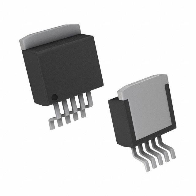
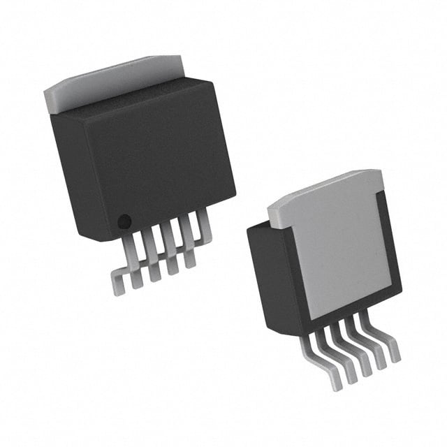
| 产品图片 |
|
| rohs | 符合RoHS无铅 / 符合限制有害物质指令(RoHS)规范要求 |
| 产品系列 | 电源管理 IC,低压差稳压器,STMicroelectronics LD29300P2M33R- |
| 数据手册 | |
| 产品型号 | LD29300P2M33R |
| 产品目录页面 | |
| 产品种类 | 低压差稳压器 |
| 供应商器件封装 | P2PAK-4 |
| 其它名称 | 497-3475-2 |
| 其它有关文件 | http://www.st.com/web/catalog/sense_power/FM142/CL1015/SC312/PF67072?referrer=70071840 |
| 包装 | 带卷 (TR) |
| 商标 | STMicroelectronics |
| 回动电压—最大值 | 700 mV at 3 A |
| 安装类型 | 表面贴装 |
| 安装风格 | SMD/SMT |
| 封装 | Reel |
| 封装/外壳 | TO-263-6,D²Pak(5 引线+接片),TO-263BA |
| 封装/箱体 | P2PAK |
| 工作温度 | -40°C ~ 125°C |
| 工厂包装数量 | 1000 |
| 最大工作温度 | + 125 C |
| 最大输入电压 | 30 V |
| 最小工作温度 | - 40 C |
| 最小输入电压 | + 2.5 V |
| 标准包装 | 1,000 |
| 电压-跌落(典型值) | 0.4V @ 3A |
| 电压-输入 | 最高 14V |
| 电压-输出 | 3.3V |
| 电压调节准确度 | 1 % |
| 电流-输出 | 3A |
| 电流-限制(最小值) | - |
| 稳压器拓扑 | 正,固定式 |
| 稳压器数 | 1 |
| 系列 | LD29300P2M |
| 线路调整率 | 0.5 % |
| 负载调节 | 1 % |
| 输入偏压电流—最大 | 20 mA |
| 输出电压 | 3.3 V |
| 输出电流 | 3 A |
| 输出端数量 | 1 Output |
| 输出类型 | Fixed |


- 商务部:美国ITC正式对集成电路等产品启动337调查
- 曝三星4nm工艺存在良率问题 高通将骁龙8 Gen1或转产台积电
- 太阳诱电将投资9.5亿元在常州建新厂生产MLCC 预计2023年完工
- 英特尔发布欧洲新工厂建设计划 深化IDM 2.0 战略
- 台积电先进制程称霸业界 有大客户加持明年业绩稳了
- 达到5530亿美元!SIA预计今年全球半导体销售额将创下新高
- 英特尔拟将自动驾驶子公司Mobileye上市 估值或超500亿美元
- 三星加码芯片和SET,合并消费电子和移动部门,撤换高东真等 CEO
- 三星电子宣布重大人事变动 还合并消费电子和移动部门
- 海关总署:前11个月进口集成电路产品价值2.52万亿元 增长14.8%


PDF Datasheet 数据手册内容提取
LD29300xx 3 A, very low drop voltage regulators Features ■ Very low dropout voltage (Typ. 0.4 at 3 A) ■ Guaranteed output current up to 3 A ■ Fixed voltage with ± 1 % tolerance at 25 °C ■ Internal current and thermal limit ■ Logic controlled electronic shutdown available TO-220 D2PAK in PPAK Description The LD29300xx is a high current, high accuracy, low-dropout voltage regulator series. These regulators feature 400 mV dropout voltage and P2PAK/A P2PAK D2PAK/A very low ground current. Designed for high current loads, these devices are also used in lower current, extremely low dropout-critical systems, where their tiny dropout voltage and ground current values are important attributes. Typical applications are in power supply switching post regulation, Series power supply for monitors, Series power supply for VCRs and TVs, Computer systems and Battery powered systems. Table 1. Device summary Part numbers Output voltages LD29300XX15 1.5 V LD29300XX18 1.8 V LD29300XX25 2.5 V LD29300XX33 3.3 V LD29300XX50 5.0 V LD29300XX80 8.0 V LD29300XX ADJ July 2008 Rev 12 1/26 www.st.com 26
Contents LD29300xx Contents 1 Diagram . . . . . . . . . . . . . . . . . . . . . . . . . . . . . . . . . . . . . . . . . . . . . . . . . . . 3 2 Pin configuration . . . . . . . . . . . . . . . . . . . . . . . . . . . . . . . . . . . . . . . . . . . 4 3 Typical application . . . . . . . . . . . . . . . . . . . . . . . . . . . . . . . . . . . . . . . . . . 5 4 Maximum ratings . . . . . . . . . . . . . . . . . . . . . . . . . . . . . . . . . . . . . . . . . . . . 6 5 Electrical characteristics . . . . . . . . . . . . . . . . . . . . . . . . . . . . . . . . . . . . . 7 6 Typical characteristics . . . . . . . . . . . . . . . . . . . . . . . . . . . . . . . . . . . . . . 14 7 Package mechanical data . . . . . . . . . . . . . . . . . . . . . . . . . . . . . . . . . . . . 17 8 Order codes . . . . . . . . . . . . . . . . . . . . . . . . . . . . . . . . . . . . . . . . . . . . . . . 24 9 Revision history . . . . . . . . . . . . . . . . . . . . . . . . . . . . . . . . . . . . . . . . . . . 25 2/26
LD29300xx Diagram 1 Diagram Figure 1. Schematic diagram for adjustable version Figure 2. Schematic diagram for fixed version * Only for version with inhibit function. 3/26
Pin configuration LD29300xx 2 Pin configuration Figure 3. Pin connections (top view) TO-220 D2PAK P2PAK P2PAK/A D2PAK/A * Not connected for fixed version. 4/26
LD29300xx Typical application 3 Typical application Figure 4. Application circuit V = V (1 + R /R ) O REF 1 2 * Only for version with inhibit function. 5/26
Maximum ratings LD29300xx 4 Maximum ratings Table 2. Absolute maximum ratings Symbol Parameter Value Unit V DC input voltage 30 (1) V I I Output current Internally limited mA O P Power dissipation Internally limited mW D T Storage temperature range -55 to 150 °C STG T Operating junction temperature range -40 to 125 °C OP 1. Above 14 V the device is automatically in shut-down. Note: Absolute maximum ratings are those values beyond which damage to the device may occur. Functional operation under these conditions is not implied. Table 3. Thermal data Symbol Parameter TO-220 D2PAK-P2PAK-D2PAK/A-P2PAK/A Unit R Thermal resistance junction-ambient 50 60 °C/W thJA R Thermal resistance junction-case 3 3 °C/W thJC 6/26
LD29300xx Electrical characteristics 5 Electrical characteristics Table 4. Electrical characteristics of LD29300#15 (I = 10 mA, T = 25 °C, V = 3.5 V, V = 2 V (1), C = 330 nF, C = 10 µF, unless otherwise O J I INH I O specified) Symbol Parameter Test conditions Min. Typ. Max. Unit Minimum operating input V I = 10mA to 3A, T = -40 to 125°C 2.5 V I voltage O J I = 10mA to 3A, V = 3 to 7V 1.485 1.5 1.515 V Output voltage O I V O T = -40 to 125°C J 1.47 1.53 ΔV Load regulation I = 10mA to 3A 0.2 1.0 % O O ΔV Line regulation V = 3 to 13V 0.06 0.5 % O I SVR Supply voltage rejection f = 120 Hz, V = 3.5 ± 1V, I = 1.5A (2) 65 75 dB I O I = 1.5A, T = -40 to 125°C 20 50 O J mA I Quiescent current I = 3A, T = -40 to 125°C 45 100 q O J V = 13V, V = GND, T = -40 to 125°C 130 180 µA I INH J I Short circuit current V - V = 5.5V 4.5 A sc I O V Control input logic low OFF MODE (1), T = -40 to 125°C 0.8 V IL J V Control input logic high ON MODE (1), T = -40 to 125°C 2 V IH J I Control input current T = -40 to 125°C, V = 13V 5 10 µA INH J INH eN Output noise voltage B = 10Hz to 100kHz, I = 100mA 60 µV P O RMS 1. Only for version with Inhibit function. 2. Guaranteed by design 7/26
Electrical characteristics LD29300xx Table 5. Electrical characteristics of LD29300#18 (I = 10 mA, T = 25 °C, V = 3.8 V, V = 2 V (1), C = 330 nF, C = 10 µF, unless otherwise O J I INH I O specified) Symbol Parameter Test conditions Min. Typ. Max. Unit I = 10mA to 3A, V = 3 to 7.3V 1.782 1.8 1.818 V Output voltage O I V O T = -40 to 125°C J 1.764 1.836 ΔV Load regulation I = 10mA to 3A 0.2 1.0 % O O ΔV Line regulation V = 3 to 13V 0.06 0.5 % O I SVR Supply voltage rejection f = 120 Hz, V = 3.8 ±1V, I = 1.5A (2) 62 72 dB I O I = 500mA, T = -40 to 125°C (3) 0.1 O J V Dropout voltage I = 1.5A, T = -40 to 125°C (3) 0.2 V DROP O J I = 3A, T = -40 to 125°C (3) 0.4 0.7 O J I = 1.5A, T = -40 to 125°C 20 50 O J mA I Quiescent current I = 3A, T = -40 to 125°C 45 100 q O J V = 13V, V = GND, T = -40 to 125°C 130 180 µA I INH J I Short circuit current V - V = 5.5V 4.5 A sc I O V Control input logic low OFF MODE (1), T = -40 to 125°C 0.8 V IL J V Control input logic high ON MODE (1), T = -40 to 125°C 2 V IH J I Control input current T = -40 to 125°C, V = 13V 5 10 µA INH J INH eN Output noise voltage B = 10Hz to 100kHz, I = 100mA 60 µV P O RMS 1. Only for version with Inhibit function. 2. Guaranteed by design. 3. Dropout voltage is defined as the input-to-output differential when the output voltage drops to 99 % of its nominal value with V + 1 V applied to V. O I 8/26
LD29300xx Electrical characteristics Table 6. Electrical characteristics of LD29300#25 (I = 10 mA, T = 25 °C, V = 4.5 V, V = 2 V (1), C = 330 nF, C = 10 µF, unless otherwise O J I INH I O specified) Symbol Parameter Test conditions Min. Typ. Max. Unit I = 10mA to 3A, V = 3.5 to 8V 2.475 2.5 2.525 V Output voltage O I V O T = -40 to 125°C J 2.45 2.55 ΔV Load regulation I = 10mA to 3A 0.2 1.0 % O O ΔV Line regulation V = 3 to 13V 0.06 0.5 % O I SVR Supply voltage rejection f = 120 Hz, V = 4.5 ±1V, I = 1.5A (2) 55 70 dB I O I = 500mA, T = -40 to 125°C (3) 0.1 O J V Dropout voltage I = 1.5A, T = -40 to 125°C (3) 0.2 V DROP O J I = 3A, T = -40 to 125°C (3) 0.4 0.7 O J I = 1.5A, T = -40 to 125°C 20 50 O J mA I Quiescent current I = 3A, T = -40 to 125°C 45 100 q O J V = 13V, V = GND, T = -40 to 125°C 130 180 µA I INH J I Short circuit current V - V = 5.5V 4.5 A sc I O V Control input logic low OFF MODE (1), T = -40 to 125°C 0.8 V IL J V Control input logic high ON MODE (1), T = -40 to 125°C 2 V IH J I Control input current T = -40 to 125°C, V = 13V 5 10 µA INH J INH eN Output noise voltage B = 10Hz to 100kHz, I = 100mA 100 µV P O RMS 1. Only for version with Inhibit function. 2. Guaranteed by design. 3. Dropout voltage is defined as the input-to-output differential when the output voltage drops to 99 % of its nominal value with V + 1 V applied to V. O I 9/26
Electrical characteristics LD29300xx Table 7. Electrical characteristics of LD29300#33 (I = 10 mA, T = 25 °C, V = 5.3 V, V = 2 V (1), C = 330 nF, C = 10 µF, unless otherwise O J I INH I O specified) Symbol Parameter Test conditions Min. Typ. Max. Unit I = 10mA to 3A, V = 4.3 to 8.8V 3.267 3.3 3.333 V Output voltage O I V O T = -40 to 125°C J 3.234 3.366 ΔV Load regulation I = 10mA to 3A 0.2 1.0 % O O ΔV Line regulation V = 4.3 to 13V 0.06 0.5 % O I SVR Supply voltage rejection f = 120 Hz, V = 5.3 ±1V, I = 1.5A (2) 52 67 dB I O I = 500mA, T = -40 to 125°C (3) 0.1 O J V Dropout voltage I = 1.5A, T = -40 to 125°C (3) 0.2 V DROP O J I = 3A, T = -40 to 125°C (3) 0.4 0.7 O J I = 1.5A, T = -40 to 125°C 20 50 O J mA I Quiescent current I = 3A, T = -40 to 125°C 45 100 q O J V = 13V, V = GND, T = -40 to 125°C 130 180 µA I INH J I Short circuit current V - V = 5.5V 4.5 A sc I O V Control input logic low OFF MODE (1), T = -40 to 125°C 0.8 V IL J V Control input logic high ON MODE (1), T = -40 to 125°C 2 V IH J I Control input current T = -40 to 125°C, V = 13V 5 10 µA INH J INH eN Output noise voltage B = 10Hz to 100kHz, I = 100mA 132 µV P O RMS 1. Only for version with Inhibit function. 2. Guaranteed by design. 3. Dropout voltage is defined as the input-to-output differential when the output voltage drops to 99 % of its nominal value with V + 1 V applied to V. O I 10/26
LD29300xx Electrical characteristics Table 8. Electrical characteristics of LD29300#50 (I = 10 mA, T = 25 °C, V = 7 V, V = 2 V (1), C = 330 nF, C = 10 µF, unless otherwise O J I INH I O specified) Symbol Parameter Test conditions Min. Typ. Max. Unit I = 10mA to 3A, V = 6 to 10.5V 4.95 5 5.05 V Output voltage O I V O T = -40 to 125°C J 4.9 5.1 ΔV Load regulation I = 10mA to 3A 0.2 1.0 % O O ΔV Line regulation V = 6 to 13V 0.06 0.5 % O I SVR Supply voltage rejection f = 120 Hz, V = 7 ±1V, I = 1.5A (2) 49 64 dB I O I = 500mA, T = -40 to 125°C (3) 0.1 O J V Dropout voltage I = 1.5A, T = -40 to 125°C (3) 0.2 V DROP O J I = 3A, T = -40 to 125°C (3) 0.4 0.7 O J I = 1.5A, T = -40 to 125°C 20 50 O J mA I Quiescent current I = 3A, T = -40 to 125°C 45 100 q O J V = 13V, V = GND, T = -40 to 125°C 130 180 µA I INH J I Short circuit current V - V = 5.5V 4.5 A sc I O V Control input logic low OFF MODE (1), T = -40 to 125°C 0.8 V IL J V Control input logic high ON MODE (1), T = -40 to 125°C 2 V IH J I Control input current T = -40 to 125°C, V = 13V 5 10 µA INH J INH eN Output noise voltage B = 10Hz to 100kHz, I = 100mA 200 µV P O RMS 1. Only for version with Inhibit function. 2. Guaranteed by design. 3. Dropout voltage is defined as the input-to-output differential when the output voltage drops to 99 % of its nominal value with V + 1 V applied to V. O I 11/26
Electrical characteristics LD29300xx Table 9. Electrical characteristics of LD29300#80 (I = 10 mA, T = 25 °C, V = 10 V, V = 2 V (1), C = 330 nF, C = 10 µF, unless otherwise O J I INH I O specified) Symbol Parameter Test conditions Min. Typ. Max. Unit I = 10mA to 3A, V = 9 to 13V 7.92 8 8.08 V Output voltage O I V O T = -40 to 125°C J 7.84 8.16 ΔV Load regulation I = 10mA to 3A 0.2 1.0 % O O ΔV Line regulation V = 9 to 13V 0.06 0.5 % O I SVR Supply voltage rejection f = 120 Hz, V = 9 ±1V, I = 1.5A (2) 45 59 dB I O I = 500mA, T = -40 to 125°C (3) 0.1 O J V Dropout voltage I = 1.5A, T = -40 to 125°C (3) 0.2 V DROP O J I = 3A, T = -40 to 125°C (3) 0.4 0.7 O J I = 1.5A, T = -40 to 125°C 20 50 O J mA I Quiescent current I = 3A, T = -40 to 125°C 45 100 q O J V = 13V, V = GND, T = -40 to 125°C 130 180 µA I INH J I Short circuit current V - V = 5.5V 4.5 A sc I O V Control input logic low OFF MODE (1), T = -40 to 125°C 0.8 V IL J V Control input logic high ON MODE (1), T = -40 to 125°C 2 V IH J I Control input current T = -40 to 125°C, V = 13V 5 10 µA INH J INH eN Output noise voltage B = 10Hz to 100kHz, I = 100mA 320 µV P O RMS 1. Only for version with Inhibit function. 2. Guaranteed by design. 3. Dropout voltage is defined as the input-to-output differential when the output voltage drops to 99 % of its nominal value with V + 1 V applied to V. O I 12/26
LD29300xx Electrical characteristics Table 10. Electrical characteristics of LD29300#ADJ (I = 10 mA, T = 25 °C, V = 3.23 V, V = 2 V (1), C = 330 nF, C = 10 µF adjust pin tied to O J I INH I O output pin) Symbol Parameter Test conditions Min. Typ. Max. Unit Minimum operating input V I = 10mA to 3A, T = -40 to 125°C 2.5 V I voltage O J ΔV Load regulation I = 10mA to 3A 0.2 1.0 % O O ΔV Line regulation V = 2.5 V to 13V 0.06 0.5 % O I I = 10mA to 3A, V = 2.5 to 4.5V -1% 1.23 +1% V Reference voltage O I V REF T = -40 to 125°C (2) J -2% +2% SVR Supply voltage rejection f = 120 Hz, V = 3.23 ±1V, I = 1.5A (3) 65 75 dB I O I = 1.5A, T = -40 to 125°C 20 50 O J mA I Quiescent current I = 3A, T = -40 to 125°C 45 100 q O J V = 13V, V = GND, T = -40 to 125°C 130 180 µA I INH J I Adjust pin current T = -40 to 125°C (3) 1 µA ADJ J I Short circuit current V - V = 5.5V 4.5 A sc I O V Control input logic low OFF MODE (1),T = -40 to 125°C 0.8 V IL J V Control input logic high ON MODE (1), T = -40 to 125°C 2 V IH J I Control input current T = -40 to 125°C, V = 13V 5 10 µA INH J INH eN Output noise voltage B = 10Hz to 100kHz, I = 100mA 50 µV P O RMS 1. Only for version with Inhibit function. 2. Reference voltage is measured between output and GND pin, with ADJ PIN tied to V . OUT 3. Guaranteed by design. 13/26
Typical characteristics LD29300xx 6 Typical characteristics Figure 5. Output voltage vs temperature Figure 6. Dropout voltage vs temperature Figure 7. Dropout voltage vs output current Figure 8. Quiescent current vs output current Figure 9. Quiescent current vs output current Figure 10. Quiescent current vs supply voltage 14/26
LD29300xx Typical characteristics Figure 11. Quiescent current vs temperature Figure 12. Quiescent current vs temperature Figure 13. Short circuit current vs temperature Figure 14. Supply voltage rejection vs temperature Figure 15. Stability vs C Figure 16. Line transient O V=3.5 to 5.5V, I =10mA, V =2.5V, C =10µF I LOAD O O 15/26
Typical characteristics LD29300xx Figure 17. Load transient V=4.5V, I =10mA to 3A, V =2.5V, C =47µF I O O O 16/26
LD29300xx Package mechanical data 7 Package mechanical data In order to meet environmental requirements, ST offers these devices in ECOPACK® packages. These packages have a lead-free second level interconnect. The category of second Level Interconnect is marked on the package and on the inner box label, in compliance with JEDEC Standard JESD97. The maximum ratings related to soldering conditions are also marked on the inner box label. ECOPACK is an ST trademark. ECOPACK specifications are available at: www.st.com. 17/26
Package mechanical data LD29300xx TO-220 (A type) mechanical data mm. inch. Dim. Min. Typ. Max. Min. Typ. Max. A 4.40 4.60 0.173 0.181 b 0.61 0.88 0.024 0.035 b1 1.15 1.70 0.045 0.067 c 0.49 0.70 0.019 0.028 D 15.25 15.75 0.600 0.620 E 10.0 10.40 0.394 0.409 e 2.4 2.7 0.094 0.106 e1 4.95 5.15 0.195 0.203 F 1.23 1.32 0.048 0.052 H1 6.2 6.6 0.244 0.260 J1 2.40 2.72 0.094 0.107 L 13.0 14.0 0.512 0.551 L1 3.5 3.93 0.138 0.155 L20 16.4 0.646 L30 28.9 1.138 φP 3.75 3.85 0.148 0.152 Q 2.65 2.95 0.104 0.116 0015988/N 18/26
LD29300xx Package mechanical data D2PAK mechanical data mm. inch. Dim. Min. Typ. Max. Min. Typ. Max. A 4.4 4.6 0.173 0.181 A1 2.49 2.69 0.098 0.106 A2 0.03 0.23 0.001 0.009 B 0.7 0.93 0.027 0.036 B2 1.14 1.7 0.044 0.067 C 0.45 0.6 0.017 0.023 C2 1.23 1.36 0.048 0.053 D 8.95 9.35 0.352 0.368 D1 8 0.315 E 10 10.4 0.393 0.409 E1 8.5 0.335 G 4.88 5.28 0.192 0.208 L 15 15.85 0.590 0.624 L2 1.27 1.4 0.050 0.055 L3 1.4 1.75 0.055 0.068 M 2.4 3.2 0.094 0.126 R 0.4 0.016 V2 0° 8° 0° 8° P011P6G 19/26
Package mechanical data LD29300xx D2PAK/A mechanical data mm. inch. Dim. Min. Typ. Max. Min. Typ. Max. A 4.40 4.60 0.173 0.181 A1 2.49 2.69 0.098 0.106 A2 0.03 0.23 0.001 0.009 B 0.7 0.93 0.028 0.037 B1 0.8 1.3 0.031 0.051 B2 1.14 1.7 0.045 0.067 C 0.45 0.60 0.018 0.024 C2 1.23 1.36 0.048 0.054 D 8.95 9.35 0.352 0.368 D1 8 0.315 E 10 10.4 0.394 0.409 E1 8.5 0.335 G 4.88 5.28 0.192 0.208 L 15 15.85 0.591 0.624 L2 1.27 1.4 0.050 0.055 M 2.4 3.2 0.094 0.126 R 0.4 0.016 V2 0° 8° 0° 8° 7106164/D 20/26
LD29300xx Package mechanical data P2PAK mechanical data mm. inch. Dim. Min. Typ. Max. Min. Typ. Max. A 4.30 4.80 0.169 0.188 A1 2.40 2.80 0.094 0.110 A2 0.03 0.23 0.001 0.009 b 0.80 1.05 0.031 0.041 c 0.45 0.60 0.017 0.023 c2 1.17 1.37 0.046 0.053 D 8.95 9.35 0.352 0.368 D2 8 0.315 E 10.00 10.40 0.393 0.409 E1 8.5 0.334 0.409 e 3.20 3.60 0.126 0.142 e1 6.60 7.00 0.260 0.275 L 13.70 14.50 0.539 0.571 L2 1.25 1.40 0.049 0.055 L3 0.90 1.70 0.035 0.067 L5 1.55 2.40 0.061 0.094 R 0.40 0.016 V2 0° 8° 0° 8° 7226255/B 21/26
Package mechanical data LD29300xx P2PAK/A mechanical data mm. inch. Dim. Min. Typ. Max. Min. Typ. Max. A 4.30 4.80 0.169 0.188 A2 0.03 0.23 0.001 0.009 C 1.17 1.37 0.046 0.053 D 2.40 2.80 0.094 0.110 D1 8.95 9.35 0.352 0.368 E 0.45 0.60 0.017 0.023 F 0.80 1.05 0.031 0.041 G 3.20 3.60 0.126 0.142 G1 6.60 7.00 0.260 0.275 H1 8.5 0.334 0.409 H2 10.00 10.40 0.393 0.409 L 15 15.85 0.590 0.624 L1 8 0.315 L2 1.27 1.40 0.050 0.055 M 2.4 3.2 0.094 0.126 R 0.40 0.016 V2 0° 8° 0° 8° 7157127/A 22/26
LD29300xx Package mechanical data Tape & reel D2PAK-P2PAK-D2PAK/A-P2PAK/A mechanical data mm. inch. Dim. Min. Typ. Max. Min. Typ. Max. A 180 7.086 C 12.8 13.0 13.2 0.504 0.512 0.519 D 20.2 0.795 N 60 2.362 T 14.4 0.567 Ao 10.50 10.6 10.70 0.413 0.417 0.421 Bo 15.70 15.80 15.90 0.618 0.622 0.626 Ko 4.80 4.90 5.00 0.189 0.193 0.197 Po 3.9 4.0 4.1 0.153 0.157 0.161 P 11.9 12.0 12.1 0.468 0.472 0.476 23/26
Order codes LD29300xx 8 Order codes Table 11. Order codes Packages Output TO-220 D2PAK D2PAK/A P2PAK (1) P2PAK/A voltage LD29300P2T15R 1.5 V LD29300D2T18R LD29300D2M18R LD29300P2T18R LD29300P2M18R 1.8 V LD29300D2M25R 2.5 V LD29300V33 LD29300D2M33R LD29300P2T33R LD29300P2M33R 3.3 V LD29300V50 LD29300D2T50R(1) LD29300D2M50R LD29300P2T50R LD29300P2M50R 5.0 V LD29300P2T80R 8.0 V LD29300P2TR LD29300P2MTR(1) ADJ 1. Available on request 24/26
LD29300xx Revision history 9 Revision history Table 12. Document revision history Date Revision Changes 21-Oct-2005 7 Order codes updated. 10-Apr-2007 8 Order codes updated. 11-May-2007 9 Order codes updated. 08-Jun-2007 10 Order codes updated. 03-Apr-2008 11 Modified: Table11 on page24. 11-Jul-2008 12 Modified: Table11 on page24. 25/26
LD29300xx Please Read Carefully: Information in this document is provided solely in connection with ST products. STMicroelectronics NV and its subsidiaries (“ST”) reserve the right to make changes, corrections, modifications or improvements, to this document, and the products and services described herein at any time, without notice. All ST products are sold pursuant to ST’s terms and conditions of sale. Purchasers are solely responsible for the choice, selection and use of the ST products and services described herein, and ST assumes no liability whatsoever relating to the choice, selection or use of the ST products and services described herein. No license, express or implied, by estoppel or otherwise, to any intellectual property rights is granted under this document. If any part of this document refers to any third party products or services it shall not be deemed a license grant by ST for the use of such third party products or services, or any intellectual property contained therein or considered as a warranty covering the use in any manner whatsoever of such third party products or services or any intellectual property contained therein. UNLESS OTHERWISE SET FORTH IN ST’S TERMS AND CONDITIONS OF SALE ST DISCLAIMS ANY EXPRESS OR IMPLIED WARRANTY WITH RESPECT TO THE USE AND/OR SALE OF ST PRODUCTS INCLUDING WITHOUT LIMITATION IMPLIED WARRANTIES OF MERCHANTABILITY, FITNESS FOR A PARTICULAR PURPOSE (AND THEIR EQUIVALENTS UNDER THE LAWS OF ANY JURISDICTION), OR INFRINGEMENT OF ANY PATENT, COPYRIGHT OR OTHER INTELLECTUAL PROPERTY RIGHT. UNLESS EXPRESSLY APPROVED IN WRITING BY AN AUTHORIZED ST REPRESENTATIVE, ST PRODUCTS ARE NOT RECOMMENDED, AUTHORIZED OR WARRANTED FOR USE IN MILITARY, AIR CRAFT, SPACE, LIFE SAVING, OR LIFE SUSTAINING APPLICATIONS, NOR IN PRODUCTS OR SYSTEMS WHERE FAILURE OR MALFUNCTION MAY RESULT IN PERSONAL INJURY, DEATH, OR SEVERE PROPERTY OR ENVIRONMENTAL DAMAGE. ST PRODUCTS WHICH ARE NOT SPECIFIED AS "AUTOMOTIVE GRADE" MAY ONLY BE USED IN AUTOMOTIVE APPLICATIONS AT USER’S OWN RISK. Resale of ST products with provisions different from the statements and/or technical features set forth in this document shall immediately void any warranty granted by ST for the ST product or service described herein and shall not create or extend in any manner whatsoever, any liability of ST. ST and the ST logo are trademarks or registered trademarks of ST in various countries. Information in this document supersedes and replaces all information previously supplied. The ST logo is a registered trademark of STMicroelectronics. All other names are the property of their respective owners. © 2008 STMicroelectronics - All rights reserved STMicroelectronics group of companies Australia - Belgium - Brazil - Canada - China - Czech Republic - Finland - France - Germany - Hong Kong - India - Israel - Italy - Japan - Malaysia - Malta - Morocco - Singapore - Spain - Sweden - Switzerland - United Kingdom - United States of America www.st.com 26/26