ICGOO在线商城 > 集成电路(IC) > PMIC - 稳压器 - 线性 > LD1086DTTR
 Datasheet下载
- 型号: LD1086DTTR
- 制造商: STMicroelectronics
- 库位|库存: xxxx|xxxx
- 要求:
| 数量阶梯 | 香港交货 | 国内含税 |
| +xxxx | $xxxx | ¥xxxx |
查看当月历史价格
查看今年历史价格
LD1086DTTR产品简介:
ICGOO电子元器件商城为您提供LD1086DTTR由STMicroelectronics设计生产,在icgoo商城现货销售,并且可以通过原厂、代理商等渠道进行代购。 LD1086DTTR价格参考¥2.63-¥3.29。STMicroelectronicsLD1086DTTR封装/规格:PMIC - 稳压器 - 线性, Linear Voltage Regulator IC Positive Adjustable 1 Output Adj to 1.25V 1.5A DPAK。您可以下载LD1086DTTR参考资料、Datasheet数据手册功能说明书,资料中有LD1086DTTR 详细功能的应用电路图电压和使用方法及教程。
STMicroelectronics的LD1086DTTR是一款线性稳压器,属于PMIC(电源管理集成电路)系列中的低压降线性稳压器。该器件具有多种应用场景,广泛应用于消费电子、工业控制、通信设备等领域。

 1. 便携式电子设备
LD1086DTTR适用于便携式电子设备,如智能手机、平板电脑、可穿戴设备等。它能够为这些设备提供稳定的电压输出,确保内部电路在不同负载条件下正常工作。其低功耗和小封装特点使其非常适合电池供电的应用,延长了设备的续航时间。

 2. 传感器与物联网设备
在物联网(IoT)应用中,LD1086DTTR可以为各种传感器模块提供稳定的电源。例如,温度传感器、湿度传感器、加速度计等需要精确的电源供应以保证测量精度。该稳压器的高精度输出电压和低噪声特性有助于提高传感器数据的准确性。

 3. 嵌入式系统
LD1086DTTR常用于嵌入式系统的电源管理部分,特别是在微控制器(MCU)、数字信号处理器(DSP)和其他低功耗处理器的应用中。它可以为这些处理器提供稳定的工作电压,确保系统在各种环境下的可靠运行。

 4. 工业自动化
在工业自动化领域,LD1086DTTR可用于为PLC(可编程逻辑控制器)、伺服驱动器、传感器等设备提供电源。其宽输入电压范围(2.5V至20V)和高达1.5A的输出电流能力,使其能够在复杂的工业环境中稳定工作,适应不同的电源需求。

 5. 医疗设备
对于医疗设备,如便携式医疗仪器、心率监测仪、血糖仪等,LD1086DTTR提供了可靠的电源解决方案。其低噪声和高精度输出特性有助于确保医疗设备的测量结果准确无误,保障患者的安全。

 6. 汽车电子
在汽车电子领域,LD1086DTTR可以用于车载信息娱乐系统、导航系统、车身控制模块等。其良好的抗干扰能力和稳定性使其能够在严苛的汽车环境中长期可靠工作。

总之,LD1086DTTR凭借其出色的性能和广泛的适用性,成为众多应用领域的理想选择。
| 参数 | 数值 |
| 产品目录 | 集成电路 (IC)半导体 |
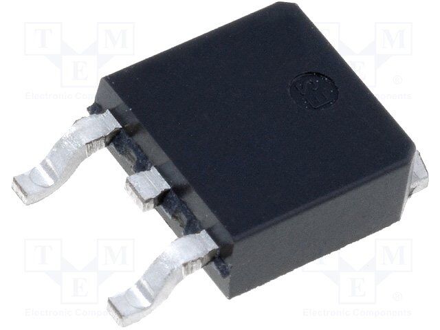
| 描述 | IC REG LDO ADJ 1.5A DPAK低压差稳压器 2.85-30V 1.5A Adj |
| 产品分类 | |
| 品牌 | STMicroelectronics |
| 产品手册 | |
| 产品图片 |
|
| rohs | 符合RoHS无铅 / 符合限制有害物质指令(RoHS)规范要求 |
| 产品系列 | 电源管理 IC,低压差稳压器,STMicroelectronics LD1086DTTRQ 汽车 |
| 数据手册 | |
| 产品型号 | LD1086DTTR |
| 产品目录页面 | |
| 产品种类 | Low Drop Voltage Regulators/Drivers |
| 供应商器件封装 | D-Pak |
| 其它名称 | 497-6222-6 |
| 其它有关文件 | http://www.st.com/web/catalog/sense_power/FM142/CL1015/SC312/SS1733/PF63445?referrer=70071840 |
| 包装 | Digi-Reel® |
| 商标 | STMicroelectronics |
| 回动电压—最大值 | 1.5 V at 1.5 A |
| 安装类型 | 表面贴装 |
| 安装风格 | SMD/SMT |
| 封装 | Reel |
| 封装/外壳 | TO-252-3,DPak(2 引线+接片),SC-63 |
| 封装/箱体 | TO-252 |
| 工作温度 | -40°C ~ 125°C |
| 工厂包装数量 | 2500 |
| 最大工作温度 | + 125 C |
| 最大输入电压 | 30 V |
| 最小工作温度 | - 40 C |
| 标准包装 | 1 |
| 电压-跌落(典型值) | 1.3V @ 1.5A |
| 电压-输入 | 最高 30V |
| 电压-输出 | 可调至 1.25V |
| 电压调节准确度 | 1 % |
| 电流-输出 | 1.5A |
| 电流-限制(最小值) | - |
| 稳压器拓扑 | 正,可调式 |
| 稳压器数 | 1 |
| 系列 | LD1086DT |
| 线路调整率 | 0.2 % |
| 负载调节 | 0.3 % |
| 输入偏压电流—最大 | 5 mA |
| 输出电压 | 1.25 V to 15 V |
| 输出电流 | 1.5 A |
| 输出端数量 | 1 Output |
| 输出类型 | Adjustable |


- 商务部:美国ITC正式对集成电路等产品启动337调查
- 曝三星4nm工艺存在良率问题 高通将骁龙8 Gen1或转产台积电
- 太阳诱电将投资9.5亿元在常州建新厂生产MLCC 预计2023年完工
- 英特尔发布欧洲新工厂建设计划 深化IDM 2.0 战略
- 台积电先进制程称霸业界 有大客户加持明年业绩稳了
- 达到5530亿美元!SIA预计今年全球半导体销售额将创下新高
- 英特尔拟将自动驾驶子公司Mobileye上市 估值或超500亿美元
- 三星加码芯片和SET,合并消费电子和移动部门,撤换高东真等 CEO
- 三星电子宣布重大人事变动 还合并消费电子和移动部门
- 海关总署:前11个月进口集成电路产品价值2.52万亿元 增长14.8%


PDF Datasheet 数据手册内容提取
LD1086 1.5 A adjustable and fixed low drop positive voltage regulator Datasheet - production data Description The LD1086 is a low drop voltage regulator capable of providing up to 1.5 A of output current. Dropout is guaranteed at a maximum of 1.2 V at the maximum output current, decreasing at lower loads. The LD1086 is pin-to-pin compatible with older 3-terminal adjustable regulators, but has DPAK better performance in terms of drop and output TO-220 tolerance. Unlike PNP regulators, where a part of the output current is wasted as quiescent current, the LD1086 quiescent current flows into the load, increasing efficiency. Only a 10 µF (minimum) capacitor is needed for stability. The device is available in a TO-220, D²PAK, D²PAK/A, DPAK or DFN8 (4x4) package. On-chip trimming allows the D²PAK DFN8 (4x4) D²PAK/A regulator to reach a very tight output voltage tolerance; within ± 1% at 25 °C. The LD1086 is available as automotive grade for adjustable Features output voltages in the TO-220 and DPAK packages. The PAT, SYL, SBL statistical tests Typical dropout: 1.3 V at 1.5 A have been performed, and the devices are Three-terminal adjustable or fixed output qualified according to the AEC-Q100 specification voltage: 1.8 V, 2.5 V, 3.3 V, 5 V, 12 V for the automotive market in the temperature range of - 40 °C to 125 °C. Automotive grade (adjustable V in TO-220 OUT and DPAK packages only) Output current guaranteed up to 1.5 A Output tolerance: ± 1% at 25 °C and ± 2% in full temperature range Internal power and thermal limit Wide operating temperature range - 40 °C to 125 °C Package available: TO-220, D²PAK, D²PAK/A, DPAK and DFN8 (4x4) Pinout compatibility with standard adjustable voltage regulators December 2017 DocID6739 Rev 36 1/42 This is information on a product in full production. www.st.com
Contents LD1086 Contents 1 Diagram . . . . . . . . . . . . . . . . . . . . . . . . . . . . . . . . . . . . . . . . . . . . . . . . . . . 5 2 Pin configuration . . . . . . . . . . . . . . . . . . . . . . . . . . . . . . . . . . . . . . . . . . . . 6 3 Maximum ratings . . . . . . . . . . . . . . . . . . . . . . . . . . . . . . . . . . . . . . . . . . . . 7 4 Schematic application . . . . . . . . . . . . . . . . . . . . . . . . . . . . . . . . . . . . . . . 8 5 Electrical characteristics . . . . . . . . . . . . . . . . . . . . . . . . . . . . . . . . . . . . . 9 6 Typical application . . . . . . . . . . . . . . . . . . . . . . . . . . . . . . . . . . . . . . . . . 17 7 Package information . . . . . . . . . . . . . . . . . . . . . . . . . . . . . . . . . . . . . . . . 22 7.1 TO-220 (STD-ST dual gauge) type A package information . . . . . . . . . . . 23 7.2 DPAK package information . . . . . . . . . . . . . . . . . . . . . . . . . . . . . . . . . . . 25 7.3 D²PAK (SMD 2L STD-ST) type A package information . . . . . . . . . . . . . . 28 7.4 D²PAK (SMD 3L STD-ST) type A package information . . . . . . . . . . . . . . 30 7.5 DPAK and D²PAK packing information . . . . . . . . . . . . . . . . . . . . . . . . . . . 33 7.6 DFN8 (4x4) package information . . . . . . . . . . . . . . . . . . . . . . . . . . . . . . . 35 7.7 DFN8 (4x4) packing information . . . . . . . . . . . . . . . . . . . . . . . . . . . . . . . . 37 8 Ordering information . . . . . . . . . . . . . . . . . . . . . . . . . . . . . . . . . . . . . . . 39 9 Revision history . . . . . . . . . . . . . . . . . . . . . . . . . . . . . . . . . . . . . . . . . . . 40 2/42 DocID6739 Rev 36
LD1086 List of tables List of tables Table 1. Absolute maximum ratings. . . . . . . . . . . . . . . . . . . . . . . . . . . . . . . . . . . . . . . . . . . . . . . . . . 7 Table 2. Thermal data. . . . . . . . . . . . . . . . . . . . . . . . . . . . . . . . . . . . . . . . . . . . . . . . . . . . . . . . . . . . . 7 Table 3. Electrical characteristics of LD1086#18 . . . . . . . . . . . . . . . . . . . . . . . . . . . . . . . . . . . . . . . . 9 Table 4. Electrical characteristics of LD1086#25 . . . . . . . . . . . . . . . . . . . . . . . . . . . . . . . . . . . . . . . 10 Table 5. Electrical characteristics of LD1086#33 . . . . . . . . . . . . . . . . . . . . . . . . . . . . . . . . . . . . . . . 11 Table 6. Electrical characteristics of LD1086#50 . . . . . . . . . . . . . . . . . . . . . . . . . . . . . . . . . . . . . . . 12 Table 7. Electrical characteristics of LD1086#12 . . . . . . . . . . . . . . . . . . . . . . . . . . . . . . . . . . . . . . . 13 Table 8. Electrical characteristics of LD1086B#. . . . . . . . . . . . . . . . . . . . . . . . . . . . . . . . . . . . . . . . 14 Table 9. Electrical characteristics of LD1086# . . . . . . . . . . . . . . . . . . . . . . . . . . . . . . . . . . . . . . . . . 15 Table 10. Electrical characteristics of LD1086DTTRY and LD1086VY (Automotive grade). . . . . . . . 16 Table 11. TO-220 (STD-ST dual gauge) type A mechanical data . . . . . . . . . . . . . . . . . . . . . . . . . . . 24 Table 12. DPAK mechanical data. . . . . . . . . . . . . . . . . . . . . . . . . . . . . . . . . . . . . . . . . . . . . . . . . . . . 26 Table 13. D²PAK (SMD 2L STD-ST) type A mechanical data . . . . . . . . . . . . . . . . . . . . . . . . . . . . . . 29 Table 14. D²PAK (SMD 3L STD-ST) type A mechanical data . . . . . . . . . . . . . . . . . . . . . . . . . . . . . . 31 Table 15. DPAK and D²PAK tape and reel mechanical data . . . . . . . . . . . . . . . . . . . . . . . . . . . . . . . 34 Table 16. DFN8 (4x4) mechanical data . . . . . . . . . . . . . . . . . . . . . . . . . . . . . . . . . . . . . . . . . . . . . . . 36 Table 17. DFN8 (4x4) reel mechanical data. . . . . . . . . . . . . . . . . . . . . . . . . . . . . . . . . . . . . . . . . . . . 37 Table 18. Order code . . . . . . . . . . . . . . . . . . . . . . . . . . . . . . . . . . . . . . . . . . . . . . . . . . . . . . . . . . . . . 39 Table 19. Document revision history . . . . . . . . . . . . . . . . . . . . . . . . . . . . . . . . . . . . . . . . . . . . . . . . . 40 DocID6739 Rev 36 3/42 42
List of figures LD1086 List of figures Figure 1. Schematic diagram. . . . . . . . . . . . . . . . . . . . . . . . . . . . . . . . . . . . . . . . . . . . . . . . . . . . . . . . 5 Figure 2. Pin connections (top view) . . . . . . . . . . . . . . . . . . . . . . . . . . . . . . . . . . . . . . . . . . . . . . . . . . 6 Figure 3. Application circuit . . . . . . . . . . . . . . . . . . . . . . . . . . . . . . . . . . . . . . . . . . . . . . . . . . . . . . . . . 8 Figure 4. Output voltage vs. temp. (VI = 5 V). . . . . . . . . . . . . . . . . . . . . . . . . . . . . . . . . . . . . . . . . . . 17 Figure 5. Output voltage vs. temp. (VI = 15 V). . . . . . . . . . . . . . . . . . . . . . . . . . . . . . . . . . . . . . . . . . 17 Figure 6. Output voltage vs. temperature (VI=4.25 V). . . . . . . . . . . . . . . . . . . . . . . . . . . . . . . . . . . 17 Figure 7. Short-circuit current vs. dropout voltage. . . . . . . . . . . . . . . . . . . . . . . . . . . . . . . . . . . . . . . 17 Figure 8. Line regulation vs. temperature . . . . . . . . . . . . . . . . . . . . . . . . . . . . . . . . . . . . . . . . . . . . . 17 Figure 9. Load regulation vs. temperature. . . . . . . . . . . . . . . . . . . . . . . . . . . . . . . . . . . . . . . . . . . . . 17 Figure 10. Dropout voltage vs. temperature . . . . . . . . . . . . . . . . . . . . . . . . . . . . . . . . . . . . . . . . . . . . 18 Figure 11. Dropout voltage vs. output current . . . . . . . . . . . . . . . . . . . . . . . . . . . . . . . . . . . . . . . . . . . 18 Figure 12. Adjust pin current vs. input voltage. . . . . . . . . . . . . . . . . . . . . . . . . . . . . . . . . . . . . . . . . . . 18 Figure 13. Adjust pin current vs. temperature . . . . . . . . . . . . . . . . . . . . . . . . . . . . . . . . . . . . . . . . . . . 18 Figure 14. Adjust pin current vs. output current. . . . . . . . . . . . . . . . . . . . . . . . . . . . . . . . . . . . . . . . . . 18 Figure 15. Quiescent current vs. output current. . . . . . . . . . . . . . . . . . . . . . . . . . . . . . . . . . . . . . . . . . 18 Figure 16. Quiescent current vs. input voltage . . . . . . . . . . . . . . . . . . . . . . . . . . . . . . . . . . . . . . . . . . 19 Figure 17. Supply voltage rejection vs. output current. . . . . . . . . . . . . . . . . . . . . . . . . . . . . . . . . . . . . 19 Figure 18. Supply voltage rejection vs. frequency. . . . . . . . . . . . . . . . . . . . . . . . . . . . . . . . . . . . . . . . 19 Figure 19. Supply voltage rejection vs. temperature . . . . . . . . . . . . . . . . . . . . . . . . . . . . . . . . . . . . . . 19 Figure 20. Minimum load current vs. temperature. . . . . . . . . . . . . . . . . . . . . . . . . . . . . . . . . . . . . . . . 19 Figure 21. Stability for adjustable. . . . . . . . . . . . . . . . . . . . . . . . . . . . . . . . . . . . . . . . . . . . . . . . . . . . . 19 Figure 22. Stability for 2.85 V. . . . . . . . . . . . . . . . . . . . . . . . . . . . . . . . . . . . . . . . . . . . . . . . . . . . . . . . 20 Figure 23. Stability for 12 V . . . . . . . . . . . . . . . . . . . . . . . . . . . . . . . . . . . . . . . . . . . . . . . . . . . . . . . . . 20 Figure 24. Line transient (VI = 12 to 13 V). . . . . . . . . . . . . . . . . . . . . . . . . . . . . . . . . . . . . . . . . . . . . . 20 Figure 25. Line transient (IO = 200 mA). . . . . . . . . . . . . . . . . . . . . . . . . . . . . . . . . . . . . . . . . . . . . . . . 20 Figure 26. Line transient (CADJ = 1 µF) . . . . . . . . . . . . . . . . . . . . . . . . . . . . . . . . . . . . . . . . . . . . . . . 20 Figure 27. Load transient. . . . . . . . . . . . . . . . . . . . . . . . . . . . . . . . . . . . . . . . . . . . . . . . . . . . . . . . . . . 20 Figure 28. Load transient (Trise = Tfall = 10 µs) . . . . . . . . . . . . . . . . . . . . . . . . . . . . . . . . . . . . . . . . . 21 Figure 29. Thermal protection . . . . . . . . . . . . . . . . . . . . . . . . . . . . . . . . . . . . . . . . . . . . . . . . . . . . . . . 21 Figure 30. TO-220 (STD-ST dual gauge) type A package outline . . . . . . . . . . . . . . . . . . . . . . . . . . . 23 Figure 31. DPAK package outline. . . . . . . . . . . . . . . . . . . . . . . . . . . . . . . . . . . . . . . . . . . . . . . . . . . . 25 Figure 32. DPAK recommended footprint (dimension are in mm) . . . . . . . . . . . . . . . . . . . . . . . . . . . 27 Figure 33. D²PAK (SMD 2L STD-ST) type A package outline . . . . . . . . . . . . . . . . . . . . . . . . . . . . . . 28 Figure 34. D²PAK (SMD 3L STD-ST) type A outline . . . . . . . . . . . . . . . . . . . . . . . . . . . . . . . . . . . . . . 30 Figure 35. D²PAK (SMD 3L) recommended footprint . . . . . . . . . . . . . . . . . . . . . . . . . . . . . . . . . . . . . 32 Figure 36. DPAK and D²PAK tape outline. . . . . . . . . . . . . . . . . . . . . . . . . . . . . . . . . . . . . . . . . . . . . . 33 Figure 37. DPAK and D²PAK reel outline . . . . . . . . . . . . . . . . . . . . . . . . . . . . . . . . . . . . . . . . . . . . . . 34 Figure 38. DFN8 (4x4) package outline. . . . . . . . . . . . . . . . . . . . . . . . . . . . . . . . . . . . . . . . . . . . . . . . 35 Figure 39. DFN8 (4x4) recommended footprint. . . . . . . . . . . . . . . . . . . . . . . . . . . . . . . . . . . . . . . . . . 36 Figure 40. DFN8 (4x4) tape outline (dimension are in mm). . . . . . . . . . . . . . . . . . . . . . . . . . . . . . . . . 37 Figure 41. DFN8 (4x4) reel outline. . . . . . . . . . . . . . . . . . . . . . . . . . . . . . . . . . . . . . . . . . . . . . . . . . . . 38 4/42 DocID6739 Rev 36
LD1086 Diagram 1 Diagram Figure 1. Schematic diagram DocID6739 Rev 36 5/42 42
Pin configuration LD1086 2 Pin configuration Figure 2. Pin connections (top view) TO-220 D²PAK DPAK D²PAK/A NC 1 8 IN NC 2 7 IN OUTPUT ADJ/GND 3 6 NC NC 4 5 NC AM11888v1 DFN8 (4x4) Note: The TAB is physically connected to the output (this is valid for the TO-220 package too). 6/42 DocID6739 Rev 36
LD1086 Maximum ratings 3 Maximum ratings Table 1. Absolute maximum ratings Symbol Parameter Value Unit V DC input voltage 30 V I I Output current Internally Limited mA O P Power dissipation Internally Limited mW D T Storage temperature range -55 to +150 °C STG T Junction temperature range -40 to +150 °C J Note: Absolute maximum ratings are those values beyond which damage to the device may occur. Functional operation under these conditions is not implied. Table 2. Thermal data D²PAK Symbol Parameter TO-220 DPAK DFN8 (4x4) Unit D²PAK/A R Thermal resistance junction-case 5 3 8 1.5 °C/W thJC R Thermal resistance junction-ambient 50 62.5 100 33 °C/W thJA DocID6739 Rev 36 7/42 42
Schematic application LD1086 4 Schematic application Figure 3. Application circuit R 2 V = V 1+------- O REF R 1 8/42 DocID6739 Rev 36
LD1086 Electrical characteristics 5 Electrical characteristics V = 4.8 V, C = C =10µF, T = -40 to 125 °C, unless otherwise specified. I I O A Table 3. Electrical characteristics of LD1086#18 Symbol Parameter Test conditions Min. Typ. Max. Unit I = 0 mA, T = 25 °C 1.782 1.8 1.818 V V Output voltage (1) O J O I = 0 to 1.5 A, V = 3.4 to 30 V 1.764 1.8 1.836 V O I I = 0 mA, V = 3.4 to 18 V, O I 0.2 4 mV VO Line regulation TJ=25°C I = 0 mA, V = 3.4 to 15 V 0.4 4 mV O I I = 0 to 1.5 A, T = 25 °C 0.5 8 mV O J V Load regulation O I = 0 to 1.5 A 1 16 mV O V Dropout voltage I = 1.5 A 1.3 1.5 V d O I Quiescent current V 30 V 5 10 mA q I V - V = 5 V 1.5 2 A I O I Short-circuit current sc V - V = 25 V 0.05 0.02 A I O Thermal regulation T = 25 °C, 30 ms pulse 0.01 0.04 %/W A f = 120 Hz, C = 25 µF, I = 1.5 A SVR Supply voltage rejection O O 60 82 dB V = 6.8 3 V I RMS output noise voltage eN T = 25 °C, f =10 Hz to 10 kHz 0.003 % (% of V ) A O S Temperature stability 0.5 % S Long term stability T = 125 °C, 1000 Hrs 0.5 % A 1. See short-circuit current curve for available output current at fixed dropout. DocID6739 Rev 36 9/42 42
Electrical characteristics LD1086 V = 5.5 V, C = C =10µF, T = -40 to 125 °C, unless otherwise specified. I I O A Table 4. Electrical characteristics of LD1086#25 Symbol Parameter Test conditions Min. Typ. Max. Unit I = 0 mA, T = 25 °C 2.475 2.5 2.525 V V Output voltage (1) O J O I = 0 to 1.5 A, V = 4.1 to 30 V 2.45 2.5 2.55 V O I I = 0 mA, V = 4.1 to 18 V, O I 0.2 4 mV VO Line regulation TJ=25 °C I = 0 mA, V = 4.1 to 18 V 0.4 4 mV O I I = 0 to 1.5 A, T = 25 °C 0.5 8 mV O J V Load regulation O I = 0 to 1.5 A 1 16 mV O V Dropout voltage I = 1.5 A 1.3 1.5 V d O I Quiescent current V 30 V 5 10 mA q I V - V = 5 V 1.5 2 A I O I Short-circuit current sc V - V = 25 V 0.05 0.2 A I O Thermal regulation T = 25 °C, 30 ms pulse 0.008 0.04 %/W A f = 120 Hz, C = 25 µF, I = 1.5 A SVR Supply voltage rejection O O 60 81 dB V = 7.5 3 V I RMS output noise voltage eN T = 25 °C, f =10 Hz to 10 kHz 0.003 % (%ofV ) A O S Temperature stability 0.5 % S Long term stability T = 125 °C, 1000 Hrs 0.5 % A 1. See short-circuit current curve for available output current at fixed dropout. 10/42 DocID6739 Rev 36
LD1086 Electrical characteristics V = 6.3 V, C = C =10µF, T = -40 to 125 °C, unless otherwise specified. I I O A Table 5. Electrical characteristics of LD1086#33 Symbol Parameter Test conditions Min. Typ. Max. Unit I = 0 mA, T = 25 °C 3.267 3.3 3.333 V V Output voltage (1) O J O I = 0 to 1.5 A, V = 4.9 to 30 V 3.234 3.3 3.366 V O I I = 0 mA, V = 4.9 to 18 V, O I 0.5 6 mV VO Line regulation TJ=25°C I = 0 mA, V = 4.9 to 18 V 1 6 mV O I I = 0 to 1.5 A, T = 25 °C 1 10 mV O J V Load regulation O I = 0 to 1.5 A 7 25 mV O V Dropout voltage I = 1.5 A 1.3 1.5 V d O I Quiescent current V 30 V 5 10 mA q I V - V = 5 V 1.5 2 A I O I Short-circuit current sc V - V = 25 V 0.05 0.2 A I O Thermal regulation T = 25 °C, 30 ms pulse 0.008 0.04 %/W A f = 120 Hz, C = 25 µF, I = 1.5 A SVR Supply voltage rejection O O 60 79 dB V = 8.3 3 V I RMS output noise voltage eN T = 25 °C, f =10 Hz to 10 kHz 0.003 % (% of V ) A O S Temperature stability 0.5 % S Long term stability T = 125 °C, 1000 Hrs 0.5 % A 1. See short-circuit current curve for available output current at fixed dropout. DocID6739 Rev 36 11/42 42
Electrical characteristics LD1086 V = 8 V, C = C =10µF, T = -40 to 125 °C, unless otherwise specified. I I O A Table 6. Electrical characteristics of LD1086#50 Symbol Parameter Test conditions Min. Typ. Max. Unit I = 0 mA, T = 25 °C 4.95 5 5.05 V V Output voltage (1) O J O I = 0 to 1.5 A, V = 6.6 to 30 V 4.9 5 5.1 V O I I = 0 mA, V = 6.6 to 20V, O I 0.5 10 mV VO Line regulation TJ=25°C I = 0 mA, V = 6.6 to 20 V 1 10 mV O I I = 0 to 1.5 A, T = 25 °C 5 20 mV O J V Load regulation O I = 0 to 1.5 A 10 35 mV O V Dropout voltage I = 1.5 A 1.3 1.5 V d O I Quiescent current V 30 V 5 10 mA q I V - V = 5 V 1.5 2 A I O I Short-circuit current sc V - V = 25 V 0.05 0.2 A I O Thermal regulation T = 25 °C, 30 ms pulse 0.01 0.04 %/W A f = 120 Hz, C = 25 µF, I = 1.5 A SVR Supply voltage rejection O O 60 75 dB V = 10 3 V I RMS output noise voltage eN T = 25 °C, f =10 Hz to 10 kHz 0.003 % (%ofV ) A O S Temperature stability 0.5 % S Long term stability T = 125 °C, 1000 Hrs 0.5 % A 1. See short-circuit current curve for available output current at fixed dropout. 12/42 DocID6739 Rev 36
LD1086 Electrical characteristics V = 15 V, C = C =10µF, T = -40 to 125 °C, unless otherwise specified. I I O A Table 7. Electrical characteristics of LD1086#12 Symbol Parameter Test conditions Min. Typ. Max. Unit I = 0 mA, T = 25 °C 11.88 12 12.12 V V Output voltage (1) O J O I = 0 to 1.5 A, V = 13.8 to 30 V 11.76 12 12.24 V O I I = 0 mA, V = 13.8 to 25 V, O I 1 25 mV VO Line regulation TJ = 25 °C I = 0 mA, V = 13.8 to 25 V 2 25 mV O I I = 0 to 1.5 A, T = 25 °C 12 36 mV O J V Load regulation O I = 0 to 1.5 A 24 72 mV O V Dropout voltage I = 1.5 A 1.3 1.5 V d O I Quiescent current V 30 V 5 10 mA q I V - V = 5 V 1.5 2 A I O I Short-circuit current sc V - V = 25 V 0.05 0.2 A I O Thermal regulation T = 25 °C, 30 ms pulse 0.01 0.04 %/W A f = 120 Hz, C = 25 µF, I = 1.5 A SVR Supply voltage rejection O O 54 66 dB V = 17 3 V I RMS output noise voltage eN T = 25 °C, f =10 Hz to 10 kHz 0.003 % (% of V ) A O S Temperature stability 0.5 % S Long term stability T = 125 °C, 1000 Hrs 0.5 % A 1. See short-circuit current curve for available output current at fixed dropout. DocID6739 Rev 36 13/42 42
Electrical characteristics LD1086 V = 4.25 V, C = C =10µF, T = -40 to 125 °C, unless otherwise specified. I I O A Table 8. Electrical characteristics of LD1086B# Symbol Parameter Test conditions Min. Typ. Max. Unit I = 10 mA T = 25 °C 1.231 1.25 1.269 V O J Vref Reference voltage (1) IO = 10 mA to 1.5 A, VI = 2.85 to 1.219 1.25 1.281 V 30V I = 10 mA, V = 2.8 to 16.5 V, O I 0.015 0.2 % VO Line regulation TJ = 25 °C I = 10 mA, V = 2.8 to 16.5 V 0.035 0.2 % O I I = 10 mA to 1.5 A, T = 25 °C 0.1 0.3 % O J V Load regulation O I = 0 to 1.5 A 0.2 0.4 % O V Dropout voltage I = 1.5 A 1.3 1.5 V d O I Minimum load current V 30 V 3 10 mA O(min) I V - V = 5 V 1.5 2.3 A I O I Short-circuit current sc V - V = 25 V 0.05 0.2 A I O Thermal regulation T = 25 °C, 30 ms pulse 0.01 0.04 %/W A f = 120 Hz, C = 25 µF,C = 25 µF, SVR Supply voltage rejection O ADJ 60 88 dB I = 1.5 A, V = 6.25 3 V O I I Adjust pin current V 4.25 V, I = 10 mA 40 120 µA ADJ I O I = 10 mA to 1.5 A, V = 2.8 to I Adjust pin current change (1) O I 0.2 5 µA ADJ 16.5V RMS output noise voltage eN T = 25 °C, f =10 Hz to 10 kHz 0.003 % (% of V ) A O S Temperature stability 0.5 % S Long term stability T = 125 °C, 1000 Hrs 0.5 % A 1. See short-circuit current curve for available output current at fixed dropout. 14/42 DocID6739 Rev 36
LD1086 Electrical characteristics V = 4.25 V, C = C =10µF, T = -40 to 125 °C, unless otherwise specified. I I O A Table 9. Electrical characteristics of LD1086# Symbol Parameter Test conditions Min. Typ. Max. Unit I = 10 mA T = 25 °C 1.237 1.25 1.263 V O J Vref Reference voltage (1) IO = 10 mA to 1.5 A, VI = 2.85 to 1.225 1.25 1.275 V 30V I = 10 mA, V = 2.8 to 16.5 V, O I 0.015 0.2 % VO Line regulation TJ = 25 °C I = 10 mA, V = 2.8 to 16.5 V 0.035 0.2 % O I I = 10 mA to 1.5 A, T = 25 °C 0.1 0.3 % O J V Load regulation O I = 0 to 1.5 A 0.2 0.4 % O V Dropout voltage I = 1.5 A 1.3 1.5 V d O I Minimum load current V 30 V 3 10 mA O(min) I V - V = 5 V 1.5 2.3 A I O I Short-circuit current sc V - V = 25 V 0.05 0.2 A I O Thermal regulation T = 25 °C, 30 ms pulse 0.01 0.04 %/W A f = 120 Hz, C = 25 µF,C = 25 µF, SVR Supply voltage rejection O ADJ 60 88 dB I = 1.5 A, V = 6.25 3 V O I I Adjust pin current V 4.25 V, I = 10 mA 40 120 µA ADJ I O I = 10 mA to 1.5 A, V = 2.8 to I Adjust pin current change (1) O I 0.2 5 µA ADJ 16.5V RMS output noise voltage eN T = 25 °C, f =10 Hz to 10 kHz 0.003 % (% of V ) A O S Temperature stability 0.5 % S Long term stability T = 125 °C, 1000 Hrs 0.5 % A 1. See short-circuit current curve for available output current at fixed dropout. DocID6739 Rev 36 15/42 42
Electrical characteristics LD1086 V = 4.25 V, C = C =10µF, T = -40 to 125 °C, unless otherwise specified. I I O A Table 1 0 . Electrical characteristics of LD1086DTTRY and LD1086VY (Automotive grade) Symbol Parameter Test conditions Min. Typ. Max. Unit I = 10 mA T = 25 °C 1.237 1.25 1.263 V V Reference voltage (1) O A ref I = 10 mA to 1.5 A, V = 2.85 to 30 V 1.225 1.25 1.275 V O I V Line regulation I = 10 mA, V = 2.8 to 16.5 V 0.035 0.2 % O O I V Load regulation I = 0 to 1.5 A 0.2 0.4 % O O V Dropout voltage I = 1.5 A 1.3 1.5 V d O I Minimum load current V 30 V 3 10 mA O(min) I V - V = 5 V, T = 25 °C 1.5 2.3 A I O A I Short-circuit current sc V - V = 25 V, T = 25 °C 0.05 0.2 A I O A Thermal regulation T = 25 °C, 30 ms pulse 0.01 0.04 %/W A f = 120 Hz, C = 25 µF,C = 25 µF, SVR Supply voltage rejection O ADJ 60 88 dB I = 1.5 A, V = 6.25 3 V, T = 25 °C O I A I Adjust pin current V 4.25 V, I = 10 mA 40 120 A ADJ I O I Adjust pin current change (1) I = 10 mA to 1.5 A, V = 2.8 to 16.5 V 0.2 5 A ADJ O I RMS output noise voltage eN T = 25 °C, f =10 Hz to 10 kHz 0.003 % (% of V ) A O S Temperature stability 0.5 % S Long term stability T = 125 °C, 1000 Hrs 0.5 % A 1. See short-circuit current curve for available output current at fixed dropout. 16/42 DocID6739 Rev 36
LD1086 Typical application 6 Typical application Unless otherwise specified T = 25 °C, C = C = 10 µF. J I O Figure 4. Output voltage vs. temp. (V = 5 V) Figure 5. Output voltage vs. temp. (V = 15 V) I I Figure 6. Output voltage vs. temperature Figure 7. Short-circuit current vs. dropout (V =4.25 V) voltage I Figure 8. Line regulation vs. temperature Figure 9. Load regulation vs. temperature DocID6739 Rev 36 17/42 42
Typical application LD1086 Figure 10. Dropout voltage vs. temperature Figure 11. Dropout voltage vs. output current Figure 12. Adjust pin current vs. input voltage Figure 13. Adjust pin current vs. temperature Figure 14. Adjust pin current vs. output current Figure 15. Quiescent current vs. output current 18/42 DocID6739 Rev 36
LD1086 Typical application Figure 16. Quiescent current vs. input voltage Figure 17. Supply voltage rejection vs. output current Figure 18. Supply voltage rejection vs. Figure 19. Supply voltage rejection vs. frequency temperature Figure 20. Minimum load current vs. Figure 21. Stability for adjustable temperature DocID6739 Rev 36 19/42 42
Typical application LD1086 Figure 22. Stability for 2.85 V Figure 23. Stability for 12 V Figure 24. Line transient (V = 12 to 13 V) Figure 25. Line transient (I = 200 mA) I O V = 12 to 13 V, I = 200 mA, C = 1 µF (tant), C = 10 µF V = 12 to 13 V, I = 200 mA, C = 1 µF (tant), C = 10 µF I O I O I O I O (tant), No C (tant), No C ADJ ADJ Figure 26. Line transient (C = 1 µF) Figure 27. Load transient ADJ V = 12 to 13 V, I = 200 mA, C = 1 µF (tant), C = 10 µF V = 13 V, I = 0.1 to 1.5 A, C = 1 µF (tant), C = 10 µF (tant) I O I O I O I O (tant), C = 1 µF C = 1 µF ADJ ADJ 20/42 DocID6739 Rev 36
LD1086 Typical application Figure 28. Load transient (T = T = 10 µs) Figure 29. Thermal protection rise fall V = 13 V, I = 0.1 to 1.5 A, C = 1 µF (tant), C = 10 µF V = 2.85 V I O I O O (tant), C = 1 µF ADJ DocID6739 Rev 36 21/42 42
Package information LD1086 7 Package information In order to meet environmental requirements, ST offers these devices in different grades of ECOPACK® packages, depending on their level of environmental compliance. ECOPACK® specifications, grade definitions and product status are available at: www.st.com. ECOPACK® is an ST trademark. 22/42 DocID6739 Rev 36
LD1086 Package information 7.1 TO-220 (STD-ST dual gauge) type A package information Figure 30. TO-220 (STD-ST dual gauge) type A package outline (cid:19)(cid:19)(cid:20)(cid:24)(cid:28)(cid:27)(cid:27)(cid:66)(cid:87)(cid:92)(cid:83)(cid:72)(cid:36)(cid:66)(cid:53)(cid:72)(cid:89)(cid:66)(cid:55) DocID6739 Rev 36 23/42 42
Package information LD1086 Table 11. TO-220 (STD-ST dual gauge) type A mechanical data mm Dim. Min. Typ. Max. A 4.40 4.60 b 0.61 0.88 b1 1.14 1.70 c 0.48 0.70 D 15.25 15.75 D1 1.27 E 10 10.40 e 2.40 2.70 e1 4.95 5.15 F 1.23 1.32 H1 6.20 6.60 J1 2.40 2.72 L 13 14 L1 3.50 3.93 L20 16.40 L30 28.90 P 3.75 3.85 Q 2.65 2.95 24/42 DocID6739 Rev 36
LD1086 Package information 7.2 DPAK package information Figure 31. DPAK package outline 0068772_K DocID6739 Rev 36 25/42 42
Package information LD1086 Table 12. DPAK mechanical data mm Dim. Min. Typ. Max. A 2.20 2.40 A1 0.90 1.10 A2 0.03 0.23 b 0.64 0.90 b4 5.20 5.40 c 0.45 0.60 c2 0.48 0.60 D 6.00 6.20 D1 5.10 E 6.40 6.60 E1 4.70 e 2.28 e1 4.40 4.60 H 9.35 10.10 L 1.00 1.50 (L1) 2.80 L2 0.80 L4 0.60 1.00 R 0.20 V2 0° 8° 26/42 DocID6739 Rev 36
LD1086 Package information Figure 32. DPAK recommended footprint (dimension are in mm) Footprint_REV_K DocID6739 Rev 36 27/42 42
Package information LD1086 7.3 D²PAK (SMD 2L STD-ST) type A package information Figure 33. D²PAK (SMD 2L STD-ST) type A package outline 0079457_T 28/42 DocID6739 Rev 36
LD1086 Package information Table 13. D²PAK (SMD 2L STD-ST) type A mechanical data mm Dim. Min. Typ. Max. A 4.40 4.60 A1 0.03 0.23 b 0.70 0.93 b2 1.14 1.70 c 0.45 0.60 c2 1.23 1.36 D 8.95 9.35 D1 7.50 E 10 10.40 E1 8.50 e 2.54 e1 4.88 5.28 H 15 15.85 J1 2.49 2.69 L 2.29 2.79 L1 1.27 1.40 L2 1.30 1.75 R 0.4 V2 0° 8° DocID6739 Rev 36 29/42 42
Package information LD1086 7.4 D²PAK (SMD 3L STD-ST) type A package information Figure 34. D²PAK (SMD 3L STD-ST) type A outline 7106164_E 30/42 DocID6739 Rev 36
LD1086 Package information Table 14. D²PAK (SMD 3L STD-ST) type A mechanical data mm Dim. Min. Typ. Max. A 4.40 4.60 A1 0.03 0.23 b 0.70 0.93 b1 0.80 1.30 b2 1.14 1.70 c 0.45 0.60 c2 1.23 1.36 D 8.95 9.35 D1 7.50 E 10 10.40 E1 8.50 e 2.54 e1 4.88 5.28 H 15 15.85 J1 2.49 2.69 L 2.29 2.79 L1 1.27 1.40 R 0.4 V2 0° 8° DocID6739 Rev 36 31/42 42
Package information LD1086 Figure 35. D²PAK (SMD 3L) recommended footprint 32/42 DocID6739 Rev 36
LD1086 Package information 7.5 DPAK and D²PAK packing information Figure 36. DPAK and D²PAK tape outline 10 pitches cumulative tolerance on tape +/- 0.2 mm Top cover P0 D P2 T tape E F K0 W B1 B0 For machine ref. only A0 P1 D1 including draft and radii concentric around B0 User direction of feed R Bending radius User direction of feed AM08852v1 DocID6739 Rev 36 33/42 42
Package information LD1086 Figure 37. DPAK and D²PAK reel outline T REEL DIMENSIONS 40mm min. Access hole At sl ot location B D C N A Full radius Tape slot G measured at hub in core for tape start 25 mm min. width AM08851v2 Table 15. DPAK and D²PAK tape and reel mechanical data Tape Reel mm mm Dim. Dim. Min. Max. Min. Max. A0 6.8 7 A 330 B0 10.4 10.6 B 1.5 B1 12.1 C 12.8 13.2 D 1.5 1.6 D 20.2 D1 1.5 G 16.4 18.4 E 1.65 1.85 N 50 F 7.4 7.6 T 22.4 K0 2.55 2.75 P0 3.9 4.1 Base qty. 2500 P1 7.9 8.1 Bulk qty. 2500 P2 1.9 2.1 R 40 T 0.25 0.35 W 15.7 16.3 34/42 DocID6739 Rev 36
LD1086 Package information 7.6 DFN8 (4x4) package information Figure 38. DFN8 (4x4) package outline DocID6739 Rev 36 35/42 42
Package information LD1086 Table 16. DFN8 (4x4) mechanical data mm. Dim. Min. Typ. Max. A 0.80 0.90 1 A1 0 0.02 0.05 A3 0,20 b 0.23 0.30 0.38 D 3.90 4 4.10 D2 2.82 3 3.23 E 3.90 4 4.10 E2 2.05 2.20 2.30 e 0.80 L 0.40 0.50 0.60 Figure 39. DFN8 (4x4) recommended footprint 36/42 DocID6739 Rev 36
LD1086 Package information 7.7 DFN8 (4x4) packing information Figure 40. DFN8 (4x4) tape outline (dimension are in mm) 7279936 Table 17. DFN8 (4x4) reel mechanical data mm. inch. Dim. Min. Typ. Max. Min. Typ. Max. A 330 12.992 C 12.8 13.0 13.2 0.504 0.512 0.519 D 20.2 0.795 N 60 2.362 T 22.4 0.882 DocID6739 Rev 36 37/42 42
Package information LD1086 Figure 41. DFN8 (4x4) reel outline 38/42 DocID6739 Rev 36
LD1086 Ordering information 8 Ordering information Table 18. Order code Packages Output TO-220 D²PAK D²PAK/A DPAK DFN8 (4x4) voltages LD1086V18-DG LD1086D2T18TR LD1086DT18TR 1.8 V LD1086DT25TR 2.5 V LD1086V33-DG LD1086D2T33TR LD1086D2M33TR LD1086DT33TR 3.3 V LD1086D2T50TR LD1086DT50TR 5.0 V LD1086D2T12TR 12.0 V LD1086V-DG LD1086D2TTR LD1086D2MTR LD1086DTTR LD1086PUR ADJ LD1086VY (1) LD1086DTTRY (2) ADJ LD1086BV-DG LD1086BD2TTR LD1086BD2MTR LD1086BDTTR ADJ 1. Automotive grade products. DocID6739 Rev 36 39/42 42
Revision history LD1086 9 Revision history Table 19. Document revision history Date Revision Changes 16-May-2006 14 Order codes updated and new template. 19-Jan-2007 15 D²PAK mechanical data updated and add footprint data. 05-Apr-2007 16 Order codes updated. 07-Jun-2007 17 Order codes updated. 19-Jul-2007 18 Add note on Figure2. 03-Dec-2007 19 Modified: Table18. 31-Jan-2008 20 Added new order codes for Automotive grade products. 18-Feb-2008 21 Modified: Table18 on page39. 14-Jul-2008 22 Modified: Table1 on page7 and Table18 on page39. Added: Table12 on page26, Figure30 on page23, Figure31 on page25, 10-Mar-2010 23 Figure31 and Figure32 on page27. 15-Nov-2010 24 Modified: RthJC value for TO-220 Table2 on page7. 11-Jul-2011 25 Modified: Figure24, Figure25 on page20 and Table18 on page39. 10-Feb-2012 26 Added: order code LD1086V-DG Table18 on page39. Added: new order code LD1086PUR Table18 on page39 and new package 15-Mar-2012 27 mechanical data DFN8 (4x4 mm) Table16 on page36, Figure38 on page35, Figure39 on page36, Figure40 on page37 and Figure41 on page38. 19-Oct-2012 28 Added: RthJA value for DPAK Table2 on page7. Modified: Output voltage in Voltage reference parameter Table8 on page14 13-Feb-2013 29 and Table10 on page16. 01-Mar-2013 30 Modified: DFN8 (4 x 4) pin configuration Figure2 on page6. Added Table8: Electrical characteristics of LD1086B# and Section7.7: DFN8 (4x4) packing information. 17-Jun-2013 31 Updated Section7: Package information and Table18: Order code. Minor text changes. RPN LD1086xx changed to LD1086. Updated the Description in cover page. Cancelled Table 1: Device summary. 22-Oct-2013 32 Updated Figure2: Pin connections (top view), Section5: Electrical characteristics, Section7: Package information and Table18: Order code. Minor text changes. Updated Table 6.: Electrical characteristics of LD1086#50, Section7: Package 18-Dec-2014 33 information and Section7.7: DFN8 (4x4) packing information. Minor text changes. Updated Table18: Order code. 10-Feb-2015 34 Minor text changes. 40/42 DocID6739 Rev 36
LD1086 Revision history Table 19. Document revision history (continued) Date Revision Changes Updated Section 7: Package information and Table 18: Order code 16-Nov-2015 35 Minor text changes. 19-Dec-2017 36 Updated T value in Table1: Absolute maximum ratings. J DocID6739 Rev 36 41/42 42
LD1086 IMPORTANT NOTICE – PLEASE READ CAREFULLY STMicroelectronics NV and its subsidiaries (“ST”) reserve the right to make changes, corrections, enhancements, modifications, and improvements to ST products and/or to this document at any time without notice. Purchasers should obtain the latest relevant information on ST products before placing orders. ST products are sold pursuant to ST’s terms and conditions of sale in place at the time of order acknowledgement. Purchasers are solely responsible for the choice, selection, and use of ST products and ST assumes no liability for application assistance or the design of Purchasers’ products. No license, express or implied, to any intellectual property right is granted by ST herein. Resale of ST products with provisions different from the information set forth herein shall void any warranty granted by ST for such product. ST and the ST logo are trademarks of ST. All other product or service names are the property of their respective owners. Information in this document supersedes and replaces information previously supplied in any prior versions of this document. © 2017 STMicroelectronics – All rights reserved 42/42 DocID6739 Rev 36
Mouser Electronics Authorized Distributor Click to View Pricing, Inventory, Delivery & Lifecycle Information: S TMicroelectronics: LD1086V LD1086V33 LD1086V18 LD1086DT33TR LD1086D2T12TR LD1086D2T18TR LD1086DT25TR LD1086DT18TR LD1086D2M33TR LD1086DT50TR LD1086D2T33TR LD1086D2TTR LD1086DTTR LD1086D2MTR LD1086D2T50TR LD1086V-DG LD1086DTTRY LD1086VY LD1086PUR LD1086BV LD1086BV- DG LD1086V18-DG LD1086BDTTR LD1086V33-DG